Embed Size (px)
Citation preview
ENABLING BIG MEMORY WITH EMERGING
TECHNOLOGIES
by
Manjunath Shevgoor
A dissertation submitted to the faculty ofThe University of Utah
in partial fulfillment of the requirements for the degree of
Doctor of Philosophy
in
Computing
School of Computing
The University of Utah
May 2016

Copyright c© Manjunath Shevgoor 2016
All Rights Reserved

T h e U n i v e r s i t y o f U t a h G r a d u a t e S c h o o l
STATEMENT OF DISSERTATION APPROVAL
The dissertation of Manjunath Shevgoor
has been approved by the following supervisory committee members:
Rajeev Balasubramonian , Chair 27-Oct-2015
Date Approved
Alan L. Davis , Member 27-Oct-2015
Date Approved
Erik L. Brunvand , Member 27-Oct-2015
Date Approved
Kenneth S. Stevens , Member 27-Oct-2015
Date Approved
Naveen Muralimanohar , Member 27-Oct-2015
Date Approved
and by Ross Whitaker , Chair/Dean of
the Department/College/School of Computing
and by David B. Kieda, Dean of The Graduate School.
ABSTRACT
The demand for main memory capacity has been increasing for many years and will
continue to do so. In the past, Dynamic Random Access Memory (DRAM) process scaling
has enabled this increase in memory capacity. Along with continued DRAM scaling, the
emergence of new technologies like 3D-stacking, buffered Dual Inline Memory Modules
(DIMMs), and crosspoint nonvolatile memory promise to continue this trend in the years
ahead. However, these technologies will bring with them their own gamut of problems. In
this dissertation, I look at the problems facing these technologies from a current delivery
perspective. 3D-stacking increases memory capacity available per package, but the increased
current requirement means that more pins on the package have to be now dedicated to
provide Vdd/Vss, hence increasing cost. At the system level, using buffered DIMMs to
increase the number of DRAM ranks increases the peak current requirements of the system
if all the DRAM chips in the system are Refreshed simultaneously. Crosspoint memories
promise to greatly increase bit densities but have long read latencies because of sneak
currents in the cross-bar. In this dissertation, I provide architectural solutions to each
of these problems. We observe that smart data placement by the architecture and the
Operating System (OS) is a vital ingredient in all of these solutions. We thereby mitigate
major bottlenecks in these technologies, hence enabling higher memory densities.

To my Wife, Parents, and the Wonderful People at the University of Utah.
CONTENTS
ABSTRACT . . . . . . . . . . . . . . . . . . . . . . . . . . . . . . . . . . . . . . . . . . . . . . . . . . . . . . . . iii
LIST OF TABLES . . . . . . . . . . . . . . . . . . . . . . . . . . . . . . . . . . . . . . . . . . . . . . . . . . . viii
ACKNOWLEDGMENTS . . . . . . . . . . . . . . . . . . . . . . . . . . . . . . . . . . . . . . . . . . . . ix
CHAPTERS
1. INTRODUCTION . . . . . . . . . . . . . . . . . . . . . . . . . . . . . . . . . . . . . . . . . . . . . . . 1
1.1 Emerging Trends . . . . . . . . . . . . . . . . . . . . . . . . . . . . . . . . . . . . . . . . . . . . . . . 11.1.1 Architecting High Capacity Memory Systems . . . . . . . . . . . . . . . . . . . . 21.1.2 Peak Current Problems in Emerging Technologies . . . . . . . . . . . . . . . . . 2
1.2 Dissertation Overview . . . . . . . . . . . . . . . . . . . . . . . . . . . . . . . . . . . . . . . . . . . 31.2.1 Thesis Statement . . . . . . . . . . . . . . . . . . . . . . . . . . . . . . . . . . . . . . . . . . 41.2.2 Addressing Peak Current Problems in 3D DRAM . . . . . . . . . . . . . . . . . 41.2.3 Addressing Peak Current Problems in Multiranked DRAM . . . . . . . . . . 51.2.4 Addressing Sneak Current Problems in Crosspoint Memories . . . . . . . . 5
2. BACKGROUND . . . . . . . . . . . . . . . . . . . . . . . . . . . . . . . . . . . . . . . . . . . . . . . . 7
2.1 DRAM Organization . . . . . . . . . . . . . . . . . . . . . . . . . . . . . . . . . . . . . . . . . . . . 72.2 Accessing Data in DRAM . . . . . . . . . . . . . . . . . . . . . . . . . . . . . . . . . . . . . . . . 8
2.2.1 Basic DRAM structure . . . . . . . . . . . . . . . . . . . . . . . . . . . . . . . . . . . . . . 82.2.2 Activate . . . . . . . . . . . . . . . . . . . . . . . . . . . . . . . . . . . . . . . . . . . . . . . . . . 82.2.3 Sense Amplifiers . . . . . . . . . . . . . . . . . . . . . . . . . . . . . . . . . . . . . . . . . . . 82.2.4 Precharge . . . . . . . . . . . . . . . . . . . . . . . . . . . . . . . . . . . . . . . . . . . . . . . . 92.2.5 Charge Pumps . . . . . . . . . . . . . . . . . . . . . . . . . . . . . . . . . . . . . . . . . . . . . 92.2.6 Destructive Read . . . . . . . . . . . . . . . . . . . . . . . . . . . . . . . . . . . . . . . . . . . 92.2.7 Reads and Writes . . . . . . . . . . . . . . . . . . . . . . . . . . . . . . . . . . . . . . . . . . 9
3. ADDRESSING PEAK CURRENT PROBLEMS IN 3D DRAM . . . . . . 11
3.1 IR Drop in 3D DRAM . . . . . . . . . . . . . . . . . . . . . . . . . . . . . . . . . . . . . . . . . . 113.2 Background . . . . . . . . . . . . . . . . . . . . . . . . . . . . . . . . . . . . . . . . . . . . . . . . . . . 13
3.2.1 2D DDR3 Memory Systems . . . . . . . . . . . . . . . . . . . . . . . . . . . . . . . . . . 133.2.2 3D-Stacked Memory . . . . . . . . . . . . . . . . . . . . . . . . . . . . . . . . . . . . . . . . 143.2.3 Power Delivery Networks . . . . . . . . . . . . . . . . . . . . . . . . . . . . . . . . . . . . 15
3.3 Methodology . . . . . . . . . . . . . . . . . . . . . . . . . . . . . . . . . . . . . . . . . . . . . . . . . . 173.4 Quantifying and Managing IR-drop . . . . . . . . . . . . . . . . . . . . . . . . . . . . . . . . 21
3.4.1 Voltage Map . . . . . . . . . . . . . . . . . . . . . . . . . . . . . . . . . . . . . . . . . . . . . . 213.4.2 IR-drop Regions . . . . . . . . . . . . . . . . . . . . . . . . . . . . . . . . . . . . . . . . . . . 233.4.3 Best- and Worst-Case Operations . . . . . . . . . . . . . . . . . . . . . . . . . . . . . . 243.4.4 Column Read/Column Write Commands . . . . . . . . . . . . . . . . . . . . . . . . 25
3.4.5 IR-drop Specific Timing Constraints . . . . . . . . . . . . . . . . . . . . . . . . . . . 253.4.6 Future DRAM Generations . . . . . . . . . . . . . . . . . . . . . . . . . . . . . . . . . . . 28
3.5 Overcoming the Constraints Imposed by IR-drop . . . . . . . . . . . . . . . . . . . . . . 283.5.1 Handling Throughput Oscillations . . . . . . . . . . . . . . . . . . . . . . . . . . . . . 293.5.2 Smart Page Placement . . . . . . . . . . . . . . . . . . . . . . . . . . . . . . . . . . . . . . 29
3.6 Architecture Simulation Methodology . . . . . . . . . . . . . . . . . . . . . . . . . . . . . . . 313.7 Results . . . . . . . . . . . . . . . . . . . . . . . . . . . . . . . . . . . . . . . . . . . . . . . . . . . . . . . 313.8 Related Work . . . . . . . . . . . . . . . . . . . . . . . . . . . . . . . . . . . . . . . . . . . . . . . . . 35
3.8.1 Voltage Aware Processor Architectures . . . . . . . . . . . . . . . . . . . . . . . . . 353.8.2 Current Aware Memory Architectures . . . . . . . . . . . . . . . . . . . . . . . . . . 353.8.3 Page Placement . . . . . . . . . . . . . . . . . . . . . . . . . . . . . . . . . . . . . . . . . . . . 363.8.4 Circuit Efforts to Reduce IR-drop. . . . . . . . . . . . . . . . . . . . . . . . . . . . . . 36
3.9 Conclusions . . . . . . . . . . . . . . . . . . . . . . . . . . . . . . . . . . . . . . . . . . . . . . . . . . . 36
4. ADDRESSING PEAK CURRENT PROBLEMS IN MULTIRANKEDDRAM . . . . . . . . . . . . . . . . . . . . . . . . . . . . . . . . . . . . . . . . . . . . . . . . . . . . . . . . . 38
4.1 DRAM Refresh . . . . . . . . . . . . . . . . . . . . . . . . . . . . . . . . . . . . . . . . . . . . . . . . 384.2 Background . . . . . . . . . . . . . . . . . . . . . . . . . . . . . . . . . . . . . . . . . . . . . . . . . . . 41
4.2.1 DRAM Basics . . . . . . . . . . . . . . . . . . . . . . . . . . . . . . . . . . . . . . . . . . . . . 414.2.2 Retention Time and Refresh Interval . . . . . . . . . . . . . . . . . . . . . . . . . . . 424.2.3 Refresh Cycle Time and Recovery time . . . . . . . . . . . . . . . . . . . . . . . . . 424.2.4 Performance Penalty from Refresh . . . . . . . . . . . . . . . . . . . . . . . . . . . . . 434.2.5 Details of DRAM Refresh . . . . . . . . . . . . . . . . . . . . . . . . . . . . . . . . . . . . 434.2.6 DRAM Scaling . . . . . . . . . . . . . . . . . . . . . . . . . . . . . . . . . . . . . . . . . . . . 444.2.7 Fine Granularity Refresh in DDR4 . . . . . . . . . . . . . . . . . . . . . . . . . . . . . 454.2.8 NVM Writes . . . . . . . . . . . . . . . . . . . . . . . . . . . . . . . . . . . . . . . . . . . . . . 46
4.3 Motivation . . . . . . . . . . . . . . . . . . . . . . . . . . . . . . . . . . . . . . . . . . . . . . . . . . . . 464.3.1 Peak Power . . . . . . . . . . . . . . . . . . . . . . . . . . . . . . . . . . . . . . . . . . . . . . . 464.3.2 Page Mapping and Stalls from Refresh . . . . . . . . . . . . . . . . . . . . . . . . . . 474.3.3 Performance with Staggered Refresh . . . . . . . . . . . . . . . . . . . . . . . . . . . 484.3.4 Impact of NVM Writes . . . . . . . . . . . . . . . . . . . . . . . . . . . . . . . . . . . . . . 50
4.4 Proposal: Rank Assignment . . . . . . . . . . . . . . . . . . . . . . . . . . . . . . . . . . . . . . 514.4.1 Current Approaches to Memory Mapping . . . . . . . . . . . . . . . . . . . . . . . 514.4.2 Overview . . . . . . . . . . . . . . . . . . . . . . . . . . . . . . . . . . . . . . . . . . . . . . . . . 534.4.3 Page Placement with Modified Clock . . . . . . . . . . . . . . . . . . . . . . . . . . . 544.4.4 Multithreaded Applications . . . . . . . . . . . . . . . . . . . . . . . . . . . . . . . . . . 56
4.5 Other Schemes Tried: Eager Refresh . . . . . . . . . . . . . . . . . . . . . . . . . . . . . . . 564.6 Methodology . . . . . . . . . . . . . . . . . . . . . . . . . . . . . . . . . . . . . . . . . . . . . . . . . . 57
4.6.1 Simulation . . . . . . . . . . . . . . . . . . . . . . . . . . . . . . . . . . . . . . . . . . . . . . . . 574.6.2 Simulator Parameters . . . . . . . . . . . . . . . . . . . . . . . . . . . . . . . . . . . . . . . 574.6.3 Peak Power Model . . . . . . . . . . . . . . . . . . . . . . . . . . . . . . . . . . . . . . . . . 584.6.4 Workloads . . . . . . . . . . . . . . . . . . . . . . . . . . . . . . . . . . . . . . . . . . . . . . . . 584.6.5 Long Simulations to Evaluate Page Allocation . . . . . . . . . . . . . . . . . . . . 59
4.7 Results . . . . . . . . . . . . . . . . . . . . . . . . . . . . . . . . . . . . . . . . . . . . . . . . . . . . . . . 594.7.1 Impact of Rank Assignment on Refresh . . . . . . . . . . . . . . . . . . . . . . . . . 594.7.2 Write Queue Drains and Bank Contention . . . . . . . . . . . . . . . . . . . . . . . 614.7.3 Page Allocation Disruptions . . . . . . . . . . . . . . . . . . . . . . . . . . . . . . . . . . 624.7.4 Handling the Long Latency of NVM Writes . . . . . . . . . . . . . . . . . . . . . . 634.7.5 Comparisons to Prior Work . . . . . . . . . . . . . . . . . . . . . . . . . . . . . . . . . . 644.7.6 Fine Granularity Refresh . . . . . . . . . . . . . . . . . . . . . . . . . . . . . . . . . . . . 64
vi
4.7.7 Adaptive Refresh . . . . . . . . . . . . . . . . . . . . . . . . . . . . . . . . . . . . . . . . . . . 654.7.8 Refresh Pausing . . . . . . . . . . . . . . . . . . . . . . . . . . . . . . . . . . . . . . . . . . . 664.7.9 Elastic Refresh . . . . . . . . . . . . . . . . . . . . . . . . . . . . . . . . . . . . . . . . . . . . 664.7.10 Summary . . . . . . . . . . . . . . . . . . . . . . . . . . . . . . . . . . . . . . . . . . . . . . . . . 684.7.11 Sensitivity Analysis . . . . . . . . . . . . . . . . . . . . . . . . . . . . . . . . . . . . . . . . . 68
4.8 Related Work . . . . . . . . . . . . . . . . . . . . . . . . . . . . . . . . . . . . . . . . . . . . . . . . . 684.9 Conclusions . . . . . . . . . . . . . . . . . . . . . . . . . . . . . . . . . . . . . . . . . . . . . . . . . . . 69
5. ADDRESSING SNEAK CURRENT PROBLEMS IN CROSSPOINTMEMORIES . . . . . . . . . . . . . . . . . . . . . . . . . . . . . . . . . . . . . . . . . . . . . . . . . . . . 71
5.1 Introduction . . . . . . . . . . . . . . . . . . . . . . . . . . . . . . . . . . . . . . . . . . . . . . . . . . 715.2 Memristor/ReRAM Technology . . . . . . . . . . . . . . . . . . . . . . . . . . . . . . . . . . . 725.3 Array Architecture . . . . . . . . . . . . . . . . . . . . . . . . . . . . . . . . . . . . . . . . . . . . . 72
5.3.1 Crossbar Architecture . . . . . . . . . . . . . . . . . . . . . . . . . . . . . . . . . . . . . . . 735.3.2 Memristor Reads/Writes . . . . . . . . . . . . . . . . . . . . . . . . . . . . . . . . . . . . . 745.3.3 Sneak Current in a Crossbar . . . . . . . . . . . . . . . . . . . . . . . . . . . . . . . . . . 75
5.4 Impact of Sneak Current . . . . . . . . . . . . . . . . . . . . . . . . . . . . . . . . . . . . . . . . . 765.4.1 Crossbar Size . . . . . . . . . . . . . . . . . . . . . . . . . . . . . . . . . . . . . . . . . . . . . . 765.4.2 Array Bandwidth . . . . . . . . . . . . . . . . . . . . . . . . . . . . . . . . . . . . . . . . . . 775.4.3 Read Complexity . . . . . . . . . . . . . . . . . . . . . . . . . . . . . . . . . . . . . . . . . . 785.4.4 Variable Write Latency . . . . . . . . . . . . . . . . . . . . . . . . . . . . . . . . . . . . . . 79
5.5 Proposal . . . . . . . . . . . . . . . . . . . . . . . . . . . . . . . . . . . . . . . . . . . . . . . . . . . . . 805.5.1 Reusing Background Currents . . . . . . . . . . . . . . . . . . . . . . . . . . . . . . . . 805.5.2 Staggered Data Mapping for High Reliability . . . . . . . . . . . . . . . . . . . . . 84
5.6 Methodology . . . . . . . . . . . . . . . . . . . . . . . . . . . . . . . . . . . . . . . . . . . . . . . . . . 875.7 Results . . . . . . . . . . . . . . . . . . . . . . . . . . . . . . . . . . . . . . . . . . . . . . . . . . . . . . . 88
5.7.1 Impact of Memristor Write Latency . . . . . . . . . . . . . . . . . . . . . . . . . . . . 935.8 Related Work . . . . . . . . . . . . . . . . . . . . . . . . . . . . . . . . . . . . . . . . . . . . . . . . . 945.9 Conclusion . . . . . . . . . . . . . . . . . . . . . . . . . . . . . . . . . . . . . . . . . . . . . . . . . . . . 94
6. CONCLUSION AND FUTURE WORK . . . . . . . . . . . . . . . . . . . . . . . . . . . 95
6.1 Contributions . . . . . . . . . . . . . . . . . . . . . . . . . . . . . . . . . . . . . . . . . . . . . . . . . 956.2 Relationship Between the Proposed Techniques . . . . . . . . . . . . . . . . . . . . . . . 976.3 Future Work . . . . . . . . . . . . . . . . . . . . . . . . . . . . . . . . . . . . . . . . . . . . . . . . . . 98
6.3.1 Mitigating the Rising Cost of Process Variation in 3D DRAM . . . . . . . 986.3.2 PDN Aware tRFC for 3D DRAM . . . . . . . . . . . . . . . . . . . . . . . . . . . . . . 986.3.3 Addressing Long Write Latencies in Memristor-based Memory . . . . . . . 99
REFERENCES . . . . . . . . . . . . . . . . . . . . . . . . . . . . . . . . . . . . . . . . . . . . . . . . . . . . . 100
vii
LIST OF TABLES
3.1 Maximum column reads allowed in each region . . . . . . . . . . . . . . . . . . . . . . . . . 27
3.2 Simulator and DRAM parameters [1]. . . . . . . . . . . . . . . . . . . . . . . . . . . . . . . . . 32
4.1 Refresh latencies for high DRAM chip capacities [2]. . . . . . . . . . . . . . . . . . . . . 44
4.2 Simulator and DRAM [3, 1] parameters. . . . . . . . . . . . . . . . . . . . . . . . . . . . . . . 57
4.3 Accesses to nonpreferred ranks. . . . . . . . . . . . . . . . . . . . . . . . . . . . . . . . . . . . . . 60
5.1 Parameters in the crossbar array model . . . . . . . . . . . . . . . . . . . . . . . . . . . . . . 88
5.2 Simulator and Memristor timing parameters. . . . . . . . . . . . . . . . . . . . . . . . . . . 89
ACKNOWLEDGMENTS
Although the first page of this dissertation has only my name, this dissertation was
possible only by the actions of many people. I would not have been able to finish my PhD
without my wife, Ashwini, literally. Back in 2011, I was sure about two things. First, I
was sure that I wanted to stay in grad school after my MS and continue towards a Ph.D.
Second, I was sure that I did not want to stay in Salt Lake City, when Ashwini was in
Dallas. It took just one phone conversation to convince her to move to SLC, and work
remotely. Working remotely sounds easy, but trust me, it is not. For three years, she put
up with early morning meetings, endless phone calls, and a husband who vanished three
times a year during paper deadlines. Hence, this Ph.D. would not have happened without
Ashwini, literally.
My parents were instrumental in getting me to grad school. Coming to the US for a
Master’s degree without funding can be financially daunting. In 2009, I was content with
staying in my comfort zone, but my mom kept pushing me to explore my options. When I
finally decided to apply for MS, I told my dad about it.“Don’t worry about it” he assured
me. From then on, I didn’t.
I had no intentions of doing a Ph.D. when I started grad school. Working with Rajeev
changed that. I am very grateful that I had Rajeev as my advisor. His humor made light
of tough situations and his high expectations kept me working hard. I consider myself very
fortunate to have had an advisor like him.
I would like to thank my committee members Al Davis, Erik Brunvand, Ken Stevens,
and Naveen Muralimanohar for constant support and feedback. I would like to thank Chris
Wilkerson and Zeshan Chishti for a wonderful experience during my internship at Intel.
I would like to thank my colleagues at the Utah-Arch Group. Manu, Ani, Kshitij, Seth
and Nil taught me the ropes when I started. I owe them a great deal. Danny, Ali, Meysam,
Akhila, Sahil, and Karl made the Utah Arch lab a great place to work.
I would like to thank Sid and Kranti for all the support and encouragement. I also want
to thank them for the wonderful home-cooked food.

Finally I would like to thank Karen and Ann for all the support and help they provided
me.
x
CHAPTER 1
INTRODUCTION
1.1 Emerging Trends
Over the past decade, devices used for personal computing have gone through a size
and functionality revolution. Handheld devices have replaced the laptop as the primary
computing device. In addition to being a device for media consumption, these devices have
also turned out to be sources of media creation. The rise of social media coupled with the
ability to create and share information has created a need to store and process extremely
large amounts of data. Concurrently, there has also been a revolution in devices that
gather user information (Global Positioning Services, location services, temperature data,
data from electronic sales, customer profiling, health data, etc.). This explosion of data has
led to the spread of warehouse-scale computers that are needed to store and process this
data. While desktop computers and mobile devices are limited to having a few gigabytes
of memory, servers with terabytes of memory capacity are becoming commonplace.
Traditionally, disks have been the preferred medium to store large databases. In recent
years there has been a growing trend to move larger portions of data from disks to memory.
This trend has been motivated by two factors. First, there has been more than a 30×
decrease in Dynamic Random Access Memory (DRAM) prices over the last decade [4].
Second, there has been an emergence of new workloads such as data analytics, cloud-based
services, web services like search and social networks, etc., which process large amounts of
data. These workloads have necessitated the use of a medium that, in addition to storage
capacity, can also provide large data bandwidth.
The RAMCloud [5] project argues that for bandwidth limited database workloads,
moving from disk-based storage to RAM-based storage can lead to a 10-1000× increase
in performance. Additionally, moving from a device that uses sequential access to a device
that uses random access can also lead to reduced software complexity and optimization
effort. The 1000× difference in access latencies also renders a caching solution useless, as
even a 1% miss rate would lead to a 10× drop in performance. Several projects such as
2
RAMCloud [5], Pregel [6], SAS in-memory analytics [7], SAP HANA in-memory computing
and in-memory database platform [8], and BerkeleyDB [9] have shown the efficacy of this
approach. Together, these factors have led to the emergence of in-memory databases.
1.1.1 Architecting High Capacity Memory Systems
Increase in DRAM capacity has largely been driven by process scaling. Increase in
DRAM density has also been accompanied by an increase in the pin bandwidth of these
DRAM devices. However, with every generation of higher bandwidth DRAM, the number
of Dual Inline Memory Modules (DIMMs) that can be plugged into a channel has decreased.
Increasing the number of drops on the DRAM channel increases noise on the channel, hence
at higher frequencies, fewer DIMMs will be supported. While the original Dual Data Rate
(DDR) standard allowed up to 4 DIMMs per channel, the DDR3 standard only supports 1
DIMM per channel at the highest data rates [10].
Recent work has suggested that even though DRAM scaling will continue in the near
future, it will be at a slower pace and will be at great cost [11]. Going forward, we
believe that the following three solutions will be used to increase memory capacity. First,
to increase the density of DRAM per package, 3-Dimensional (3D) die stacking will be
used. 3D die stacking comes in many forms. Commercial products that package multiple
DRAM dies in the same package have been around for a few years. 2.5D packaging
using an interposer die has recently been adopted in high end iGraphics Processing Units
(GPU). Architectures that use a large number of Through Silicon Vias (TSV) to increase
performance in addition to increasing bit density will soon be commercially available.
Second, to overcome the problem of decreasing DIMM count per channel, the DRAM
command and data bus are going to be buffered. Buffering the bus reduces the number
of drops on the bus, and hence reduces noise on the channel. Approaches such as Fully
Buffered DIMM (FB-DIMM) [12], Registered DIMM (R-DIMM) [13], Load Reduced DIMM
(LR-DIMM) [14], as well as Buffer-on-Board [10] approaches such as the Intel Scalable
Memory Buffer [15] are already commercially available. Third, nonvolatile technologies
such as Phase Change Memory (PCM) and Memristor-based memory have better scaling
characteristics. Memristor memory further promises to increase density by using Crosspoint
structures that do not use an access transistor and hence have higher bit densities.
1.1.2 Peak Current Problems in Emerging Technologies
Increasing bit densities have an impact on the amount of current that is consumed in
the system. Increasing the amount of DRAM present inside a package using 3D-stacking
3
also increases the amount of current that is consumed inside the package. To supply this
additional current, a larger number of Through Silicon Vias (TSVs) and C4 bumps now
needs to be dedicated to providing power and ground. A higher count of TSVs and pins
increase chip area as well as packaging complexity, both of which increase cost.
DRAM refresh happens to be the most current intensive action performed by the DRAM
chip. As the number of ranks present in the system increases, the peak current that needs
to be supplied to refresh all the ranks in the system also increases. Even though this spike
in power only lasts as long as the refresh cycle time of DRAM, the power supplies in the
system need to be able to supply this increased current, thus increasing the total cost of
the system.
Nonvolatile memories like PCM and Memristor memory store data in the form of
resistance. These resistive technologies do not face many of the challenges that DRAM
faces at smaller geometries. Unlike PCM, the resistance of a Memristor cell is nonlinear. It
depends on the programmed state of the cell as well as the voltage applied to it. Because of
this nonlinearity, Memristor-based memories can be built in the form of a cross point array,
obviating the need for an access transistor. However, in the absence of an access transistor,
the cross point array gives rise to sneak currents. These sneak currents increase read
complexity and have a detrimental impact on the reliability of Memristor-based memory.
1.2 Dissertation Overview
From these trends, we see the need for higher memory capacities being driven by
increased data generation as well as the pervasive use of applications that require higher
data bandwidth. While traditional process scaling has been driving increasing chip densities
in the past, the technologies that will enable higher densities in the future are not without
their challenges. In this dissertation, we focus on the problems stemming from the increased
current demands, and provide architectural solutions to these problems. In Chapter 3, we
develop a static IR-drop model for 3D-stacked DRAM, where I stands for current, and
R stands for resistance of the power deliver network. We show how carefully scheduled
activities in DRAM banks can keep IR-drop under control. This allows acceptable perfor-
mance even with an under-provisioned power delivery network. In Chapter 4, we analyze
the performance loss due to staggered refresh. Staggering refresh of the ranks in the system
decreases the peak power consumed by the DRAM system. However, doing so increases
the performance loss due to refresh. We analyze the reasons for the performance loss, and
provide data placement solutions that reduce the performance loss to refresh. In Chapter 5,
4
we analyze the impact of sneak currents on read latency and read reliability. We propose a
technique that reduces the read latency and a data mapping scheme that increases reliability.
1.2.1 Thesis Statement
The memory capacity requirements of servers are increasing at a very fast rate. New
technologies (e.g., 3D-stacking, buffered DIMMs, and Memristors) will be leveraged to boost
memory capacity, but these technologies suffer from many new problems. In particular,
management of current and voltage is voltage is crucial for the efficient deployment of
new technologies. We hypothesize that architecture/OS policies for data placement can
help manage currents in memory, thus significantly impacting performance, reliability, and
power-efficiency.
1.2.2 Addressing Peak Current Problems in 3D DRAM
3D-stacking of DRAM brings with it the promise of increased bit density per package
as well as the ability to integrate different process technologies into the same package. Die
stacking can take many forms. DRAM packages that stack independent dies in a waterfall
model [16] have been around for many years. High Bandwidth Memory [17] that uses a
silicon interposer to increase the number of pins coming out of DRAM has recently been
adopted in high end graphics processors. In this work, we focus on a 3D-stack that resembles
the Hybrid Memory Cube [18].
One of the roadblocks to the adoption of a new technology is cost. This work tries to
reduce the number of TSVs and C4 bumps that are used in a 3D-stacked DRAM device,
thus leading to lower die area and a simpler package. Reducing the number of Vdd/Vss
TSVs and bumps impacts the performance by lowering the number of commands that can be
executed in parallel. By constructing a detailed Spice model of the power delivery network,
we are able to discern the exact amount of parallelism that different parts of the die stack
can afford. By creating different constraints for different regions, we are no longer limited
to the worst case constraints of the entire stack. Further, we propose a data placement
scheme that leverages the heterogeneity in the activity allowed in different regions. We are
thus able to achieve performance that is very close to the performance of an unconstrained
die stack, while greatly reducing the number of TSVs and bumps that are dedicated to the
power delivery network.
5
1.2.3 Addressing Peak Current Problems in Multiranked DRAM
A DDR3 memory controller must issue a refresh command every 7.8µs to every rank. As
the capacity of a DRAM device increases, so does the number of rows present in every bank
of DRAM, leading to an increase in the time it takes to refresh the DRAM device. DRAM
refresh also happens to be the most current intensive operation performed by DRAM. To
avoid a spike in current consumption, memory controllers stagger the refresh commands
to different ranks in the memory system. This work analyzes the performance impact of
staggering refresh. We propose an OS-based data placement scheme that tries to limit the
number of ranks occupied by a single thread. The result is that we are able to outperform
staggered refresh, while avoiding the peak power penalties of staggered refresh. Further, we
make an observation that the effect of write queue drains in nonvolatile memories manifest
in ways that are very similar to DRAM refresh. Hence, the same data placement scheme
that was proposed to address DRAM refresh is also applicable to the problem of long latency
writes in nonvolatile memories.
1.2.4 Addressing Sneak Current Problems in Crosspoint Memories
As the area of the DRAM cell is decreased, the capacitance of the DRAM cell needs
to stay the same [11]. To keep the capacitance constant, the aspect ratio of the DRAM
cell needs to keep increasing with every generation. Eventually, this leads to manufacturing
difficulties. Because of their dependence on material properties rather than the need to
store charge, nonvolatile resistive memories are more amenable to smaller geometries than
capacitive memories like DRAM [19]. Additionally, because of the inherent nonlinearity of
the resistance of Memristor cells, Memristor-based memories can be built using crosspoint
structures. Crosspoint structures do not use an access transistor, which means that a
Memristor cell only occupies an area of 4F 2. However, lack of the access transistor gives
rise to sneak currents. The current that is read out of the bitline is the current through the
selected cell, as well as the sneak current that is leaking through other cells in the bitline.
This not only increases read complexity, but also increases read latency. Read becomes a
two-step process. The first step reads only the sneak currents, and the second step reads the
actual current. The difference in the currents indicates the value stored in the cell. Sneak
currents also affect the voltage at the selected cell, which in turn affects read margins. Cells
that are furthest from the drivers are affected more than the cells that are closer to the
drivers. This work proposes a read technique where the sneak current measurement is reused
across subsequent reads from the same column of the array, thus reducing read latency. We
also propose a data mapping scheme that prevents certain cache lines from having all their
6
bits mapped to the least reliable parts of the array, thus improving reliability.
The three subsequent chapters share the same end goal: to support high capacity
memory systems. They address different problems, all rooted in the system’s inability to
manage high currents in the memory system. They provide solutions that share a common
thread – smart placement of application data in memory regions.
CHAPTER 2
BACKGROUND
In this chapter, we briefly look at the organization of a DRAM system. In Chapter 2.1,
we describe the logical organization of DDR3-based DRAM systems. In Section 2.2, we
describe the various steps involved in accessing data that is stored in DRAM.
2.1 DRAM Organization
Data stored in DRAM are accessed at the granularity of a cacheline. DDR3-based
memory systems use a cacheline width of 64 Bytes (512 bits). The DRAM system is
organized in terms of channels, ranks, and banks.
A DDR3 channel is the set of wires that connect the processor to the DRAM chips. The
channel is made up of a data bus and a command/address bus. The data bus is 64 bits
wide, and the command/address bus is 17 bits wide. If Error Correcting Codes are used,
the data bus is 72 bits wide.
DRAM chips are soldered onto boards called Dual Inline Memory Modules (DIMMs)
that are connected to the DRAM channel. Depending on the frequency of the DRAM
channel, multiple DIMMs may be connected to each DRAM channel.
Each DIMM is made up of ranks. DRAM chips that work in lock step to provide 1
cacheline worth of data make up a rank. The number of chips in a rank is determined by
the number of data pins on the DRAM chips. An xN chip has N data pins on it. For
example, a rank made of x8 chips consists of 8 chips if the rank is connected to a 64 bit
wide channel. Each chip in the rank produces 64 bits out of the 512 bits that make up
a cacheline. Data are transferred to the processor in a burst of 4 clock cycles. Data are
transferred on both the rising and falling edges of the clock, hence the name Double Data
Rate (DDR) memory.
A chip is further divided into banks. Each bank in a DRAM chip is an independent
entity that is able to produce 64 bits of data. Logically, the bank is the smallest unit in the
8
DRAM chip. However, physically a DRAM bank is made of arrays. DDR3 chips are made
up of 8 banks, DDR4 chips are made up of 16.
2.2 Accessing Data in DRAM
2.2.1 Basic DRAM structure
Data in DRAMs are stored in capacitors in the form of charge. The cell capacitor is
accessed through an access transistor. The gate terminal of the capacitor is connected to
the wordline, and the source/drain terminals are connected to the cell capacitor and the
bitline. The bitline is called so because this is the wire through which the bit stored in
the capacitor is accessed. These 1-Transistor-1-Capacitor (1T1C) structures are arranged
in 2-Dimensional (2D) grids called arrays. All the cells in a row share a common wordline
that is connected to the gate of the access transistor of each cell. All the cells in a column
share a bitline that is connected to the drain/source of the access transistor.
2.2.2 Activate
To read the data stored in this array, the wordline, which is connected to the gate
terminal of the access transistor, is turned ON. Activating the wordline connects the cell
capacitor to the bitline. The charge that is stored in the cell is now shared with the bitline.
Because DRAM is primarily optimized for the cost-per-bit metric, the DRAM cell needs to
be as small as possible. Hence, the capacitance of the DRAM cell is an order of magnitude
(12x [20]) smaller than the capacitance of the wordline. The change in voltage of a capacitor
is proportional to the charge that is injected. Because of the relatively small capacitance
of the DRAM cell when compared to the bitline, the change in bitline voltage is relatively
small.
2.2.3 Sense Amplifiers
To sense this small perturbation in the bitline, circuits called sense amps are used. Sense
amps are two input, two output differential amplifiers. If the voltage at both inputs is the
same, then the outputs are the same as the inputs. However, if there is a small difference
in the inputs, the sense amps push the output voltages apart. These are positive feedback
circuits, where the outputs are connected back to the inputs. So driving the outputs apart
also drives the inputs apart. The voltages at the sense amp terminals continue diverging
until they reach the full rail voltage.
9
2.2.4 Precharge
Before a DRAM cell is sensed, the voltage at the bitlines needs to be equalized. The
voltages are raised to Vcc/2, where Vcc is the full rail voltage. To sense data, the sense
amps need to see a change in the voltage on one of the bitlines. In order to achieve this,
the bitline is connected to a voltage of Vcc/2 and then disconnected and left hanging.
The capacitance that is associated with the bitline maintains the bitline voltage at Vcc/2.
Additionally, precharging also reduces the time the sense amp will take to raise the voltage
to Vcc. Before a precharge is issued, the wordline is de-activated, thereby closing the row
and disconnecting all DRAM cells from bitlines. Because the bitlines are directly connected
to the sense amps, precharging the bitlines also destroys the contents in the sense amp.
2.2.5 Charge Pumps
If the capacitors in the DRAM cell are charged to a voltage of Vcc, the voltage applied
to the gate of the access transistor is also Vcc, then the voltage reaching the bitline will be
at the most (V cc − V t) (where Vt is the threshold voltage of the access transistor). This
would further decrease change in voltage of the bitline due to the DRAM cell, making it
harder for the sense amp to interpret the value stored in the DRAM cell. To over come this,
the wordline driving the access transistors is driven to a voltage higher than Vcc. Charge
Pumps are used to increase the wordline voltage over the full rail voltage.
2.2.6 Destructive Read
When a DRAM row is activated, all the cells in that row are now connected to their
bitlines. The voltage in these cells is now equal to the bitline voltage. The voltage on the
bitline is slightly above or below Vcc/2, depending on the value stored. Once the bitlines
are perturbed, the sense amps start to amplify this by driving the bitline voltages. Only
when the bitline voltage reaches a sufficiently high value can the value be read out of the
row. The DRAM cells have to wait for the sense amps to drive the bitlines to full rail
voltages before their values are restored. Only once the values are restored can the row be
closed and the bitlines precharged.
2.2.7 Reads and Writes
So far we have seen how to get data out of the arrays and into the sense amps. In
order to read a cache line out of the sense amps, the column address is provided and the
Column Access Strobe (CAS) signal is asserted. The data that are currently residing in the
relatively weak bitline sense amps are then routed to the much more powerful Input-Output
10
(IO) sense amps through the column decoder. The time taken by the data to reach the DQ
pins after the CAS signal is asserted is called the CAS latency. However, since the data are
internally pipelined, the next column of the same row can be read after tCCD cycles.
To write a line into DRAM, the data at the DQ pins of the DRAM chips are driven by
the IO sense amps to the bitline sense amps. Because the IO sense amps are much more
powerful, they are able to overdrive and change the value of the bitline sense amps. The
time it takes for the data to reach the the DRAM arrays after the burst of data has been
sent is called tWR, which is the write latency.

CHAPTER 3
ADDRESSING PEAK CURRENT
PROBLEMS IN 3D DRAM
Capacity, bandwidth, and power remain critical bottlenecks in memory systems. Die
stacking using Through Silicon Vias (TSV) promises to address these bottlenecks in one form
or another. Stacking DRAM dies in the same package increases the bit density per package.
Stacking DRAM dies over a logic layer can greatly increase the functionality of the stack.
Recent products like the Hybrid Memory Cube [21, 18] and High Bandwidth Memory [17]
leverage the increased bandwidth afforded by 3-Dimensional (3D) stacking. Recent works
have explored several applications for 3D-stacking such as Near Data Computing [22],
building accelerators for specific applications [23, 24], and increasing memory capacities
by interconnecting these stacks [25, 26, 27].
One of the main impediments to the adoption of any new technology is cost. In this
chapter, we attempt to lower the cost of die stacking by reducing the pins and TSVs
that are dedicated to the power delivery network of the die stack. Reducing the pins and
TSVs increases the resistance of the Power Delivery Network (PDN) and hence decreases
the number of reads and writes that can be serviced in parallel inside the 3D-stack. In
Section 3.5, we propose a data placement scheme that is able to tolerate the decreased
activity, while limiting the performance loss.
3.1 IR Drop in 3D DRAM
DRAM supply voltages have been dropping every generation in order to improve power
efficiency in DRAM. However, as supply voltage decreases, circuits become increasingly
more sensitive to power supply noise. A 100 mV supply noise on a 1 V system is a much
greater threat to correctness than on a 2.5 V system. Traditionally, Power Delivery Networks
in DRAMs have not received much attention, but with the move towards high performance
and low-voltage DRAM, managing power supply noise becomes increasingly critical for
correctness and performance [28].
12
Of the hundreds of pins on a chip, more than half are used to supply power and ground.
These power pins are scattered across the chip so that the supply current need not travel very
far on the chip. Some of the supplied voltage is dropped across the PDN; by Ohm’s Law,
this is a function of the supplied current I and the effective resistance of the PDN R. This
is commonly referred to as “IR-drop”. If the IR-drop is very high, a lower supply voltage
is delivered to the chip’s circuits, possibly leading to incorrect operation. For example, in
commercial DDR3 DRAM chips [29](page 111), if the supply voltage is rated at 1.5 V, the
minimum allowed voltage at the circuits is specified to be 1.425 V, i.e., up to 75 mV can
be dropped across the PDN.
The IR-drop becomes unacceptable if the DRAM chip is either drawing too much power,
or if the PDN’s resistance is too high. The latter is kept in check by using many pins for
power delivery and ensuring that current travels relatively short distances. The former
is kept in check by imposing limits on the maximum activity on the chip. For example,
DRAM chips allow a maximum of 4 row activations within the timing window tFAW.
Other examples also exist, such as the timing window tRRD [30](page 429), which imposes
a minimum gap between consecutive DRAM activates1.
Technology and market forces are raising the values of I and R. First, the onset of 3D-
stacking will increase the current draw I per package. Micron has announced the imminent
release of its 3D-stacked memory+logic device, the Hybrid Memory Cube (HMC). There will
likely be other similar products, including some that only stack multiple DRAM dies [31].
Second, 3D-stacks introduce a vertical resistive component (e.g., through silicon vias or
TSVs) within the PDN, thus increasing R. Third, DRAM memory devices are highly cost
sensitive. The packaging cost of the device is a linear function of the number of pins. This
is nicely illustrated by Dong et al. [32]. They show that for a 3D-stacked device, increasing
the pin count from 600 to 900 leads to approximately a 1.5X increase in packaging cost. To
reduce cost, there is pressure to reduce pin count. Similarly, to improve data bandwidth,
there is pressure to allocate more pins for data signals. Both will reduce the pins available
for power delivery, thus potentially increasing R.
With such future 3D-stacked memory devices in mind, we carry out a detailed circuit-
level static IR-drop analysis. We then show that without additional current limiting
constraints, the level of activity (current draw) can lead to IR-drop violations. The activity
on the device must be throttled to avoid these IR-drop violations. We make the key
1Some of these constraints are influenced not just by the PDN, but also by the charge pumps. We expandon this in Section 3.4.
13
observation that IR drop not only depends on the number of banks that are servicing
requests, but also on the location of these banks and the DRAM commands being executed.
We characterize how IR-drop varies with activity distribution across banks on the 3D
device. Thus, architectural policies can play a role in dictating the maximum IR-drop,
and hence the performance and the packaging cost of a device. These observations lead us
to introduce a number of IR-drop-aware rules within the memory controller. However, this
basic design yields performance that is 4.7× lower than a memory device with an unrealistic
over-provisioned PDN that never has IR-drop violations.
We show that most of this steep performance loss can be recovered with smarter ar-
chitectural policies implemented in the memory scheduler and in the OS page manager.
The memory scheduler is designed to better handle frequent starvation scenarios. We also
introduce a dynamic page migration scheme that identifies critical pages and places them
in the regions with the highest immunity to IR-drop. With these policies in place, the new
design has performance that is only 1.2× lower than the unrealistic ideal PDN.
A few caveats are worth noting: (i) There are potentially many ways to tackle the IR-
drop problem (more pins, more TSVs, fatter wires/TSVs, new materials, voltage regulators,
higher supply voltage, in-package decaps, etc.) and the magnitude of the problem in future
technologies is yet unclear. The goal of this chapter is to explore an architectural approach
to the problem. If successful, this approach may obviate the need for more expensive
approaches, or it may be one of many solutions that are deployed to handle voltage problems.
(ii) There are many possible sources of voltage noise and this work only focuses on analyzing
static IR-drop. Note that other voltage noise sources may eat into the votage margins,
resulting in even lower tolerance for static IR-drop. A holistic architectural solution that
can cope with several voltage noise sources is left as future work. This chapter therefore
represents an initial solution to a complex problem.
3.2 Background
3.2.1 2D DDR3 Memory Systems
A modern-day memory system is implemented with DIMMs that contain commodity
2D DRAM chips that comply with the DDR3 or DDR2 standard. The processor socket
typically has up to 4 memory controllers that are used to drive 4 DDR3 memory channels.
These channels are wide (64 or 72 bits for data) and run at frequencies that are roughly
half that of the processor frequency. The channel is essentially a bus that connects to
multiple DIMMs. If more DIMMs are placed on the channel, the increased noise forces
14
the channel to operate at a lower frequency. This leads to a capacity-bandwidth trade-off.
Some recent high-capacity systems have tried to provide high capacity and high bandwidth
by introducing buffer chips on the board [10]. In such systems, the processor memory
controllers drive narrow high-speed buses that each connect to a single buffer chip. This
buffer chip then uses wide and slow DDR3 channels to connect to multiple DIMMs [33].
The buffer-on-board solution does incur a steep power penalty.
Each DDR3 DRAM chip typically organizes its data arrays into 8 banks. Each bank can
be concurrently processing a different memory transaction. To access data in a bank, the
memory controller first issues a row activate (ACT) command that brings data in a row of
cells to the row buffer. Individual cache lines in the row are read and written with column
read (COL-RD) and column write (COL-WR) commands. Before accessing a different row,
the bitlines are equalized with a precharge (PRE) command.
Even though the banks can all be busy at the same time, because of limitations on current
draw, the memory controller is restricted to issuing no more than 4 row activations within
a time period defined by the tFAW timing constraint. Further, the tRRD timing parameter
enforces a gap between activations to different banks. This current draw limitation is in
turn defined by the charge pumps provisioned on the chip and the power delivery network
that feeds these charge pumps.
3.2.2 3D-Stacked Memory
3D-stacking is being widely employed within prototype memory devices [18, 34, 35].
Of these devices, we use Micron’s Hybrid Memory Cube (HMC) as an evaluation platform
because it will soon be commercially available and several design details are already available
in the public domain [18, 36, 37]. The ideas and analyses in this chapter will apply to almost
any 3D-stacked memory device. In fact, these ideas are a better fit for cost-constrained
3D-stacked DRAM devices that do not include a logic layer. Most of our analysis is therefore
focused on the IR-drop caused by the current drawn by the DRAM stack.
The HMC stacks 4 or 8 DRAM chips on a logic layer, thus providing high capacity in a
package. It replaces several on-board interconnects with power-efficient through-silicon vias
(TSVs). It provides high internal bandwidth with many TSVs and high external bandwidth
by implementing high-speed signaling circuits on the logic layer.
The HMC architecture implements 32 banks on each DRAM die. An HMC with 8
DRAM dies has 256 independent banks. These 256 banks are organized into 16 vaults. A
vault is a vertical pillar of data that contains 2 banks from each of the 8 dies. The banks
in a vault share a single set of TSVs for data transfer. An entire cache line can be accessed
15
from a single bank in a single HMC, similar to single subarray access [38] for low energy
and limited overfetch.
The first-generation HMC uses 1866 total TSVs at 60µm pitch and 256 signal pins [37].
The external links are driven by high-frequency SerDes circuits on the logic chip. The HMC
is a high-power, high-bandwidth, and high-cost design point. 3D-stacked DRAM packages
that exclude a logic layer and high-speed SerDes links will likely be constructed with much
fewer TSVs and external pins for power and ground.
Like most memory products, there will be a push to lower cost by reducing TSVs and
pin counts, while still supporting high activity levels within 3D-stacked DRAM. The power
delivery network for the package will dictate various timing constraints (similar to tFAW
and tRRD) that will throttle the peak current drawn by the package.
3.2.3 Power Delivery Networks
The aggregate current drawn by a 3D-stacked memory device is expected to be much
higher than that of a 2D DRAM chip [37, 36]. High peak currents can have many adverse
effects, such as static IR-drop, dynamic IR-drop, power supply noise, and higher tempera-
tures. Of these, we focus on static IR-drop in this chapter.
Power is delivered through pins on the package and C4 bumps on the device. A number
of TSVs are used to carry power/ground signals from the C4 bumps to each chip on the
stack. The metal layers for the chip implement a horizontal grid of power/ground wires that
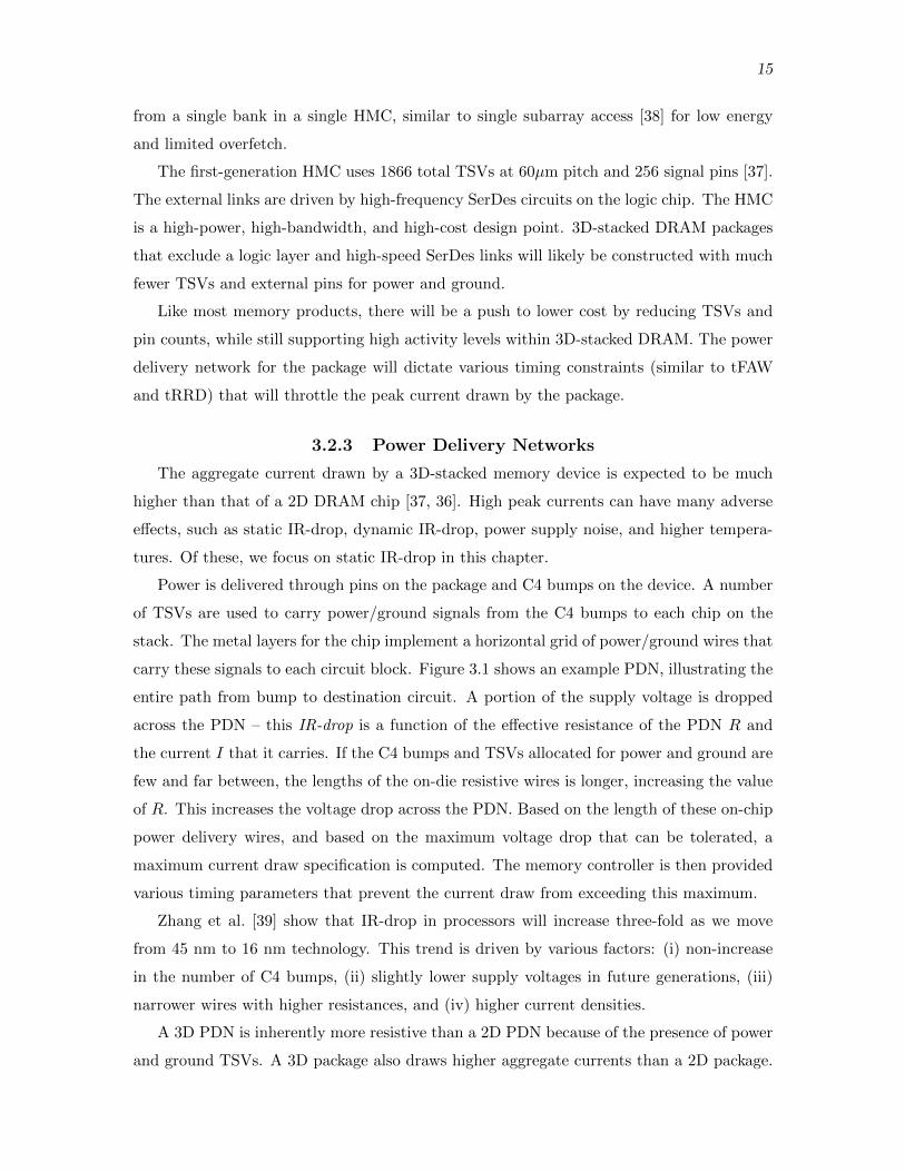
carry these signals to each circuit block. Figure 3.1 shows an example PDN, illustrating the
entire path from bump to destination circuit. A portion of the supply voltage is dropped
across the PDN – this IR-drop is a function of the effective resistance of the PDN R and
the current I that it carries. If the C4 bumps and TSVs allocated for power and ground are
few and far between, the lengths of the on-die resistive wires is longer, increasing the value
of R. This increases the voltage drop across the PDN. Based on the length of these on-chip
power delivery wires, and based on the maximum voltage drop that can be tolerated, a
maximum current draw specification is computed. The memory controller is then provided
various timing parameters that prevent the current draw from exceeding this maximum.
Zhang et al. [39] show that IR-drop in processors will increase three-fold as we move
from 45 nm to 16 nm technology. This trend is driven by various factors: (i) non-increase
in the number of C4 bumps, (ii) slightly lower supply voltages in future generations, (iii)
narrower wires with higher resistances, and (iv) higher current densities.
A 3D PDN is inherently more resistive than a 2D PDN because of the presence of power
and ground TSVs. A 3D package also draws higher aggregate currents than a 2D package.
16
C4 BUMPPROVIDINGPOWER ORGROUND
VIA
CIRCUIT BLOCKON SILICON LAYER
POWER &GROUNDGRID ON
2 METAL LAYERS
ADDITIONALLAYERS OF
SILICON & METALIN THE 3D STACK
TSV
Figure 3.1: Illustrative cross-section of a portion of the power delivery network. VDDand VSS are supplied through C4 bumps and fed to the circuit block with vias/TSVs andhorizontal power/ground grids on metal layers.
Khan et al. [40] report that when moving from 2D to 3D ICs, the IR-drop is greater than
the Ldi/dt voltage droop. Thus, there are many indications that the IR-drop problem will
be significant in future 3D devices.
Some prior work [41, 31] has attempted to design a better TSV network to reduce
IR-drop. However, these typically introduce more TSVs, which impacts cost [42], while
not eliminating the IR-drop problem. Voltage regulators [43] can also help alleviate the
IR-drop problem, but may not be viable the DRAM space because of their negative impact
on density and cost.
Assuming that the IR-drop can be tolerated, there is a strong motivation to reduce
the number of pins, C4 bumps, and TSVs allocated for power/ground. There is a linear
relationship between packaging cost and pin/C4 count [32, 44, 30]. Dong et al. [32] shows
that for a 3D-stacked device, increasing the pin count from 600 to 900 leads to approximately
a 1.5X increase in packaging cost. Packaging costs have already started exceeding silicon IC
17
fabrication costs [44]. Routing many C4 bumps through the Redistribution Layer (RDL)
inside the package incurs additional cost. Increased package routing density can lead to
decreased packaging yield and lead to increased packaging cost [45]. This steers the cost-
sensitive DRAM industry towards lower pin/C4 counts. Similarly, a high TSV count also
negatively impacts area, routing, yield, and cost.
IR-drop analysis in the PDN can be broken down into static and dynamic components.
In static IR-drop analysis, static current loads are assumed to be driven by the PDN. The
PDN is reduced to a resistive network and the voltage drop across this resistive network
is calculated based on a given current source. Dynamic IR-drop analysis takes circuit
switching as well as the capacitive and inductive nature of the PDN and the package into
account. When dynamic current consumption is simulated, PDN noise such as ground and
power bounce can be analyzed. In 2D DRAM chips, dynamic IR-drop is alleviated with
decoupling capacitors (Decaps) [30]. While a 3D package can provision more Decaps than
a 2D package, it is not clear how dynamic IR-drop will scale in future technologies.
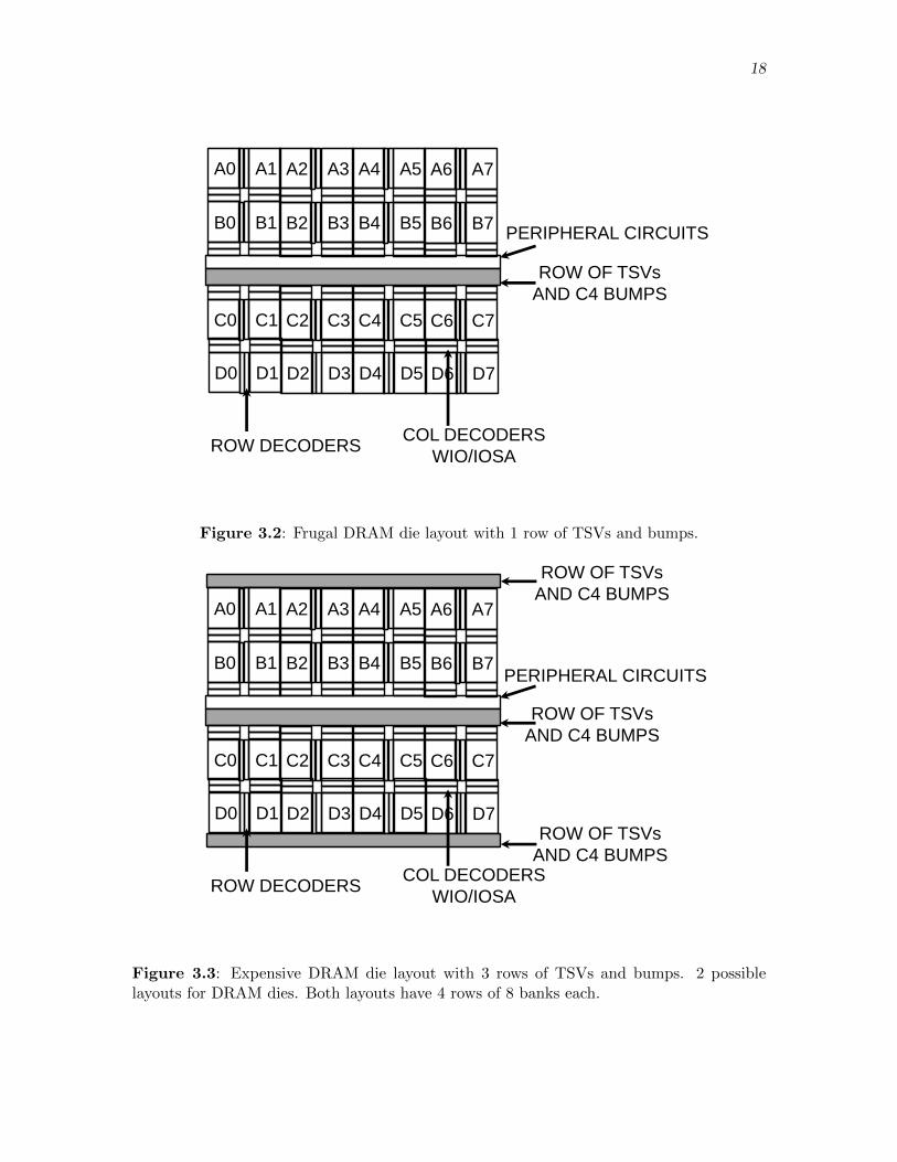
3.3 Methodology
We first explain in detail our methodology to simulate IR-drop within an HMC-style
3D-stack. This methodology takes into account the impact of TSVs, C4 bumps, and bank
activities on voltage drops within the PDN. We use the layout of Samsung’s 4-stacked 3D
design as a starting point [31]. That package includes 4 2 Gb chips. We extrapolate it
to an 8 Gb design by quadrupling the number of banks. The 2 Gb chip has 8 banks; the
HMC design has 32 independent banks in each die. So our layout replicates each bank
4 times. We also consider a shrink factor of 0.8 in the linear dimension (0.64 for area)
because of moving from a 50 nm technology to a 40 nm technology. The estimated chip
area is 13.52×16.72mm2, which is about 2.3 times larger than the 2 Gb DDR3 chip at
50 nm. The final layout (Frugal) is shown in Figure 3.2. Unlike a 2D DRAM floor plan,
which only has 1 row of banks on either side of the C4 bumps, the 32 bank floor plan will
have 2 rows of banks on each side of the C4 bumps. The 32 banks are organized as 4 rows
of 8 banks each; the banks in each row are referred to as A0 − A7, B0 − B7, C0 − C7,
and D0 −D7. Most low-cost commodity DRAM chips assume C4 bumps along the center
stripe. Kang et al. [31] show that C4 bumps and TSVs along the center can lead to a
severe IR-drop problem. They overcome this problem by introducing rows of bumps/TSVs
at the top and bottom of the chip (see the strips at the top and bottom of the expensive
layout in Figure 3.3). This is a relatively costly method to combat the problem because
18
A0 A1
B0 B1
A2 A3
B2 B3
A4 A5
B4 B5
A6 A7
B6 B7
C0 C1 C2 C3 C4 C5 C6 C7
D0 D1 D2 D3 D4 D5 D6 D7
ROW OF TSVs
AND C4 BUMPS
PERIPHERAL CIRCUITS
ROW DECODERSCOL DECODERS
WIO/IOSA
Figure 3.2: Frugal DRAM die layout with 1 row of TSVs and bumps.
ROW OF TSVs
AND C4 BUMPSA0 A1
B0 B1
A2 A3
B2 B3
A4 A5
B4 B5
A6 A7
B6 B7
C0 C1 C2 C3 C4 C5 C6 C7
D0 D1 D2 D3 D4 D5 D6 D7
ROW OF TSVs
AND C4 BUMPS
ROW OF TSVs
AND C4 BUMPS
PERIPHERAL CIRCUITS
ROW DECODERSCOL DECODERS
WIO/IOSA
Figure 3.3: Expensive DRAM die layout with 3 rows of TSVs and bumps. 2 possiblelayouts for DRAM dies. Both layouts have 4 rows of 8 banks each.
19
it requires more bumps/TSVs that impact area, yield, and packaging cost. We therefore
restrict ourselves to the Frugal layout in this study and attempt to address the IR-drop
problem with architectural solutions.
The power grid specifications used in our model are adopted from Wu et al. [46]. Due
to the back to back arrangement of banks, we assume 2X wider wires for power and ground
signals to reduce their resistances. We increase the wire width from 2 µm to 4 µm, while
keeping the pitch of the supply wires fixed at 12 µm. The assumption is that the pitch
of the supply wires is wide enough for signal wires and that routing tools may be able to
accommodate the wider wires with a minimal impact on area.
In our evaluations, we model 536 C4 bumps and 536 TSVs for power and ground. The C4
bumps have a pitch of 120 µm. The TSVs in our design are placed with a pitch of 40 µm [47].
We also assume an additional 256 signal C4 bumps and 992 signal TSVs. Similar to the
floorplan used by Kang et al. [31], the layout assumes that the top of the center stripe
accommodates peripheral circuits, while the bottom of the center stripe accommodates
TSVs and bumps. Because of this, the banks in the bottom half of the chip are closer to
the power source and exhibit a lower IR-drop. As we show later, this has a small impact
on the level of activity allowed in each bank.
We also confirmed that our TSV count is large enough to provide the necessary current
in the DRAM stacks. Using a migration density threshold of 7400 A/cm2 [48], and assuming
50% derate, 5 W requirement in the DRAM stacks, and 25 µm microbump diameter for
TSVs, we would need a minimum of 229 power and 229 ground TSVs. If we make more
pessimistic assumptions regarding the current-carrying capability of lead-free solder or the
size of the bumps, it is possible to hit the current wall before a possible IR-drop violation,
i.e., for acceptable operation, we would provision enough TSVs that static IR-drop would
not be a problem.
This work doesn’t focus on IR-drop within the logic die as a logic process has other
orthogonal approaches to combat IR-drop (more metal layers for example). The logic die
also doesn’t suffer from IR-drop across TSVs. Also, a logic chip will typically be absent in
a cost-constrained memory device. We model the power of the logic die based on values
provided for the Micron HMC [37] and assume that the power is uniformly distributed
across the logic chip. We note that the assumptions for the logic chip have a small impact
on the IR-drop within the DRAM chips. This is because the DRAM die and the logic die
only share the resistance of a small segment of C4 bumps, so a high current draw in the
logic chip only exposes the DRAM chip to a negligible amount of IR-drop.
20
We use Synopsys HSPICE Version C-2009.09-SP1 64-BIT to model voltage drops. We
model a 3D mesh of wire resistances, similar to models used in prior work [49]. The mesh
includes 3 metal layers each for 9 different dies. Capacitances are not required because this
is a static-IR model. We therefore only provide resistance values per wire and current draw
values based on the activity in a bank. The netlist was created using a Perl script. The
grid of resistance which forms the PDN is connected to the VDD and VSS bumps on one
side and is connected to circuit elements on the other side. Circuit elements connected to
the PDN are modeled as current sources which draw a fixed amount of current. The values
of resistances of metal wires, TSVs, and bumps are adopted from measured values in prior
work [46, 47, 50]. These values are 0.031, 0.196, and 0.224 Ω/ (read as Ohms per square,
which is the unit of sheet resistance) for the 3 metal layers, and 0.25 Ω for C4+TSV.
External power (VDD) is supplied at 1.5 V, the same as the DDR3 specification. We
could have also used the HMC’s 1.2 V specification, but other parameters, such as current
draw and resistances are not known. Hence, we restrict ourselves to the DDR3 model where
more parameters are known. The specification requires that the voltage at the circuits
(VDD-VSS, effective drain-to-source voltage) not drop below 1.425 V, i.e., we can tolerate
a maximum IR-drop of 75 mV. Values for current consumed within the DRAM chip are
from Micron’s data sheets [1]. Note that regardless of the assumed supply voltage, DRAM
arrays will have small margins for IR-drop. This is because DRAM arrays are designed to
operate at as high a supply voltage as possible. If DRAM arrays were designed to operate
at lower supply voltages, they would suffer from higher leakage currents and high Refresh
overheads (another emerging bottleneck in future DRAM cells).
Every DRAM operation will introduce a voltage drop in the PDN. According to Micron
data sheets, the highest current is drawn by the COL-RD command, followed by COL-WR,
and ACT/PRE. This is discussed in more detail in Section 3.4. We simulate the IR-drop
caused by column read, column write, activate, and precharge. Using the results from these
simulations, we create constraints for each of these commands. These constraints ensure
that at no time does the IR-drop go above 75 mV. These constraints are similar in spirit to
today’s DDR3 specification that disallows more than 4 ACTs within a tFAW time window.
Because modern 2D devices do not allow other commands to be issued during a Refresh
cycle, we do not model IR-drop caused by Refresh. Future 3D devices may allow activ-
ities in some banks while other banks are Refreshing. Such a model would require more
sophisticated IR-drop analyses and memory controllers.
We validate our Power Delivery Network model by making sure that the IR-drop does
21
not exceed the 75 mV constraints when a 2D 8Gb, 8-bank chip, is executing 4 activates and
a column read. The 4 activate limit is imposed by tFAW, and at any time a 2D DRAM chip
can only execute a single column read (unlike the 3D dies used in our design). Therefore,
this combination gives the highest activity that can be seen on a 2D DRAM chip. We locate
the activates and the column read in banks that are most susceptible to IR-drop to model
the worst case.
3.4 Quantifying and Managing IR-drop
We start by performing an analysis on a 3D memory stack under specific sequences of
bank operations. We observe the IR-drop in each case, focusing in particular on worst-case
access patterns that cause IR-drop to exceed the 75 mV limit or best-case access patterns
that yield acceptable IR-drop. We then draw upon these observations to develop a broad
set of guidelines that can be used to influence the behavior of the memory controller. We
also show how the memory controller and operating system would exploit these guidelines
to improve performance. The methodology for constructing the PDN is validated by first
creating the PDN for an 8-bank, 8Gb 2D DRAM die. We see that in the 2D case, the PDN
easily accommodates 4 activates in parallel, as well as a column read.
Multiple factors make IR-drop worse in the 32-bank 8-die case. The TSVs introduce a
new source of IR-drop. The lateral wiring on each die also sees a higher current. This is
because there are 4 rows of banks and multiple banks (e.g., A0 and B0) receive their power
from the same set of lateral wires. In the 8-bank 2D case, every bank has its dedicated set
of wires within the power grid. To alleviate this problem in the 32-bank 8-die design, the
power and ground wires have to be made 2x wider.
3.4.1 Voltage Map
We first illustrate the basic IR-drop phenomenon with a voltage map across all 8 DRAM
dies (die layers 2-9). Figure 3.4 and Figure 3.5 show the IR-drop in the top and bottom
DRAM dies. In this experiment, we assume that activates are happening in all the 256
banks on the 3D-stack. This is an unrealistic scenario and the IR-drop is unusually high
because of the high current draw. The figure is only meant to illustrate the banks that
experience lower voltages than others, and are therefore more prone to IR-drop violations.
The red regions are areas that receive less than the minimum required 1.425 V, making
them unreliable.
We observe that as we move up the various layers in the stack, IR-drop becomes worse
since we traverse the TSVs all the way up. Note that even though TSVs are low resistance,
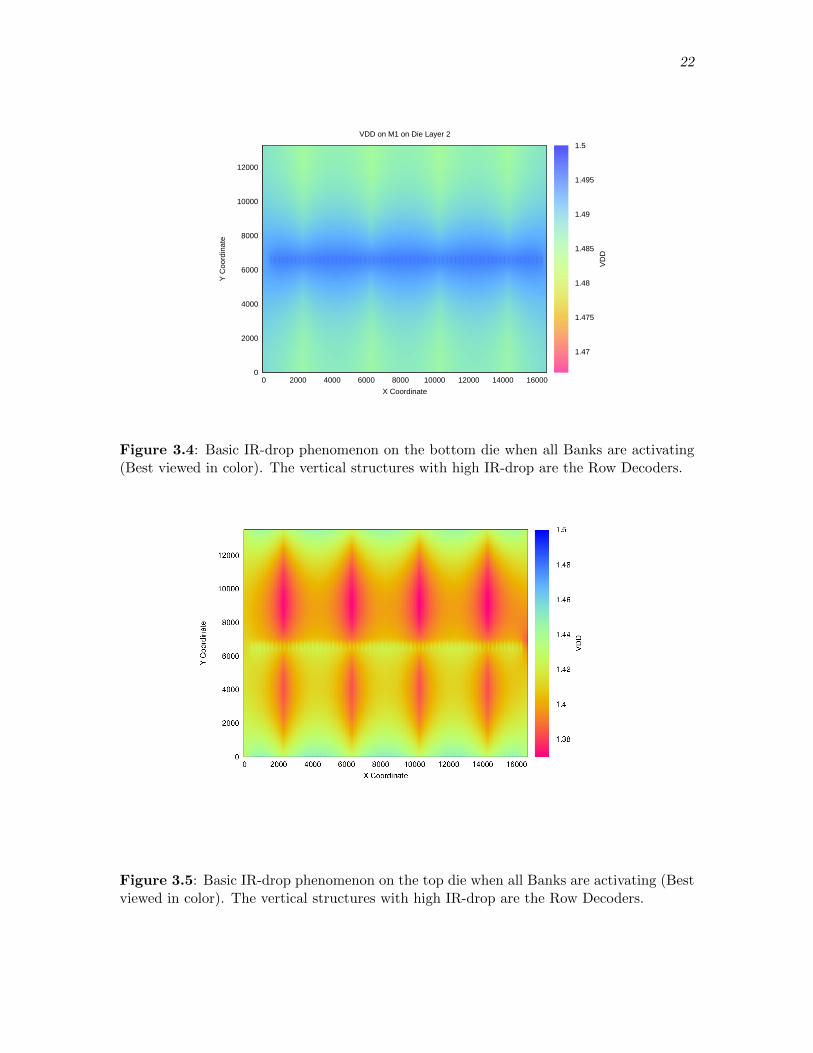
22
0
2000
4000
6000
8000
10000
12000
0 2000 4000 6000 8000 10000 12000 14000 16000
Y C
oord
inat
e
X Coordinate
VDD on M1 on Die Layer 2
1.47
1.475
1.48
1.485
1.49
1.495
1.5
VD
D
Figure 3.4: Basic IR-drop phenomenon on the bottom die when all Banks are activating(Best viewed in color). The vertical structures with high IR-drop are the Row Decoders.
Figure 3.5: Basic IR-drop phenomenon on the top die when all Banks are activating (Bestviewed in color). The vertical structures with high IR-drop are the Row Decoders.
23
they are relatively small in number, and are responsible for carrying significant amounts of
current to the upper dies, resulting in a larger IR-drop. So, in general, bottom dies are more
favorable than top dies. Similarly, as we move laterally away from the row of power pins in
the center of each die, IR-drop becomes progressively worse. Because the bump/TSV row
is in the bottom half of the center stripe, the bottom 2 rows of banks (C and D) are slightly
closer to the power source than the top 2 rows of banks (A and B), and hence experience
lower IR-drop.
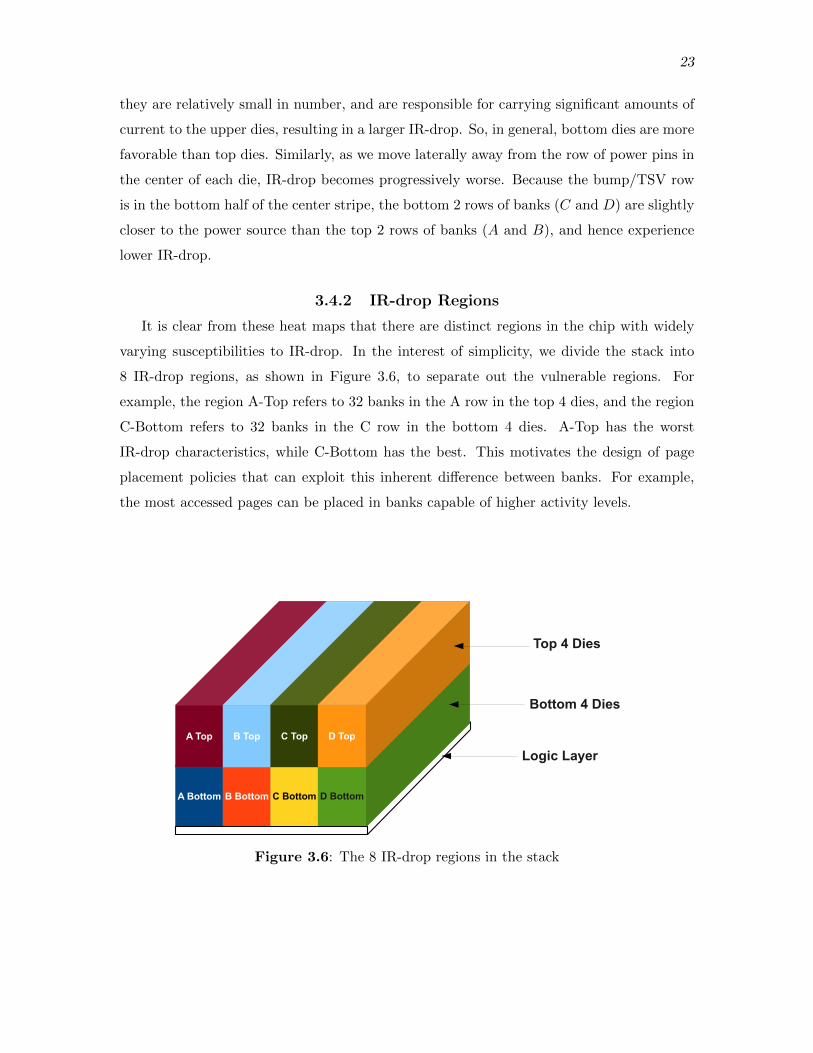
3.4.2 IR-drop Regions
It is clear from these heat maps that there are distinct regions in the chip with widely
varying susceptibilities to IR-drop. In the interest of simplicity, we divide the stack into
8 IR-drop regions, as shown in Figure 3.6, to separate out the vulnerable regions. For
example, the region A-Top refers to 32 banks in the A row in the top 4 dies, and the region
C-Bottom refers to 32 banks in the C row in the bottom 4 dies. A-Top has the worst
IR-drop characteristics, while C-Bottom has the best. This motivates the design of page
placement policies that can exploit this inherent difference between banks. For example,
the most accessed pages can be placed in banks capable of higher activity levels.
Figure 3.6: The 8 IR-drop regions in the stack
24
3.4.3 Best- and Worst-Case Operations
Next, we examine the impact on IR-drop if the 3D-stack is asked to service N simulta-
neous operations; an operation can be any of read, write, activate, or precharge. For the
purposes of this study, we assume that command bandwidth is not a constraint – this is a
reasonable assumption to make given that an HMC part will likely have multiple channels
communicating to the processor and a request buffer. These N operations can be distributed
among the 256 DRAM banks in(256N
)ways, ruling out the possibility of an exhaustive study.
Later, in the results section, we develop some guidelines for the combinations of operations
that tend to behave well or poorly.
The high-level insight from that analysis is as follows.
• For any operation, moving to higher die layers or moving away from the center TSV
strip causes higher IR-drop, because of the longer distances that the current needs to
travel.
• Banks at the edge of the die experience higher IR-drops, especially banks A0, D0, A7,
D7. This is because those banks are not supplied from all sides.
• Since the row decoders of the 2 banks in a vault lie right next to each other, activating
both banks causes large IR-drops. Row decoders are placed adjacent to each other so
that some control circuits, DC generators, and decoupling caps can be shared.
• Simultaneous operations in banks that share PDN wires (A0 and B0 for example)
yield higher IR-drops.
• Lastly, having operations in the same bank in adjacent dies increases the current
density in the shared power TSVs.
All the patterns mentioned here lead to increased current density in either the wires or
the TSVs, leading to possible IR-drop violations.
Based on this insight, we are able to estimate the best-case and worst-case scenarios when
activating banks. For example, if asked to do 8 activates in the B-top region, minimum
IR-drop is experienced by placing 4 activates in the B0 vault (one in each of the 4 top dies)
and 4 activates in the B2 vault (one in each of the 4 top dies). The maximum IR-drop is
experienced when placing 4 activates in the top die at banks B0, B1, B2, and B3, and 4
more activates in the same banks directly below. In all of our allocations, we ensure that
a single die is never asked to perform more than 4 simultaneous activates because, similar
to the tFAW constraint, the charge pumps on a single die are only provisioned to handle at
most 4 simultaneous activates.
25
3.4.4 Column Read/Column Write Commands
In 2D DRAM chips, violations are either caused when the charge pumps are depleted
or when IR-drop is high. In 2D DRAM chips, the charge pump violations typically happen
before IR-drop violations. Hence, a larger focus is placed on activates. Activates consume
more charge and dissipate higher average power than column read/write. Activates occur
for the duration of tRAS, which is much longer than the duration for a column read/write
(tDATA TRANS). This is why timing constraints (tFAW, tRRD) in 2D DRAM chips refer
to the rate at which activates can be performed.
For the reasons mentioned earlier, IR-drop is much more severe in 3D-stacks and IR-drop
violations are encountered before charge pump depletions. IR-drop is influenced more by
peak power than average power. Column read/write instantaneous current (IDD4R/IDD4W)
is 3x the instantaneous current for activates (IDD0). As a result, the focus must shift from
activates to column read/write.
The following is a brief explanation for why column read/write has higher peak power
than an activate. The data sensing during an activate is done by the Bit Line Sense Amps
(BLSA, referred to as Local and Global sense amps in [51]). During a column read, the
data have to be moved from the BLSAs, which are adjacent to the arrays, to the IO-Sense
Amps (IOSA), which are in the center stripe. Also, the data transfer needs to happen at
the speed of the channel (vault) clock, which is in the range of Gigahertz. These factors
make IDD4R very high.
While it is possible to come up with rules for every possible combination of read, write,
activate, and precharge, such a list for the 256 banks in the die stack would make the
controller intractably complex. In order to simplify the rules for the memory controller, we
define the impact of each operation in terms of the impact of a column read. For example,
we define that 2 activates correspond to one column read. This means that the worst
IR-drop caused by 2 activates cannot be greater than the least IR-drop caused by a column
read. Even though IDD4W is less than IDD4R, we find that 2 banks cannot perform writes
in parallel, without exceeding the IR-drop caused by a column read. So one column write
is deemed equivalent to one column read. Finally, 6 precharges are equivalent to a single
column read.
3.4.5 IR-drop Specific Timing Constraints
To keep the memory controller simple, it must only encode the worst-case guideline.
For example, in a given region, in the best case, IR-drop may not be violated with 8 reads.
But in the worst case, IR-drop may be violated with just 5 reads. To reduce complexity,
26
we may want to enforce the rule that the region can safely accept only 5 reads. To accept
any more reads, the memory controller would have to maintain a very large table of safe
read combinations. Hence, for each region, we do a number of Spice simulations to find the
worst-case read combinations and the minimum number of reads that lead to an IR-drop
violation. Using the PDN described in Section 3.3, we simulate the voltage in each region
when that region performs the worst-case pattern of N reads. When 1 region is receiving
reads, we assume that the other regions are idle. The data show that regions A-Top and
D-Top can only safely handle a single read at a time. With a worst-case pattern, just 2
reads can lead to a voltage under 1.425 V. Thus, regardless of what else is happening on the
3D-stack, the memory controller must enforce that these regions never service more than 1
read at a time. This rule is especially restrictive because these 4 regions are the furthest
from the power sources at the center stripe. B-Top and C-Top can service up to 2 reads at
any time. For each of the other 4 regions, we can safely service as many as 4 reads even
with the worst-case patterns, without violating IR-drop. Note that 4 is the upper-bound for
a region because there are only 4 vaults available per region. In other words, the 4 regions
A-Bot, B-Bot, C-Bot, and D-Bot, are relatively unconstrained by IR-drop because of their
proximity to the power source.
The previous discussion assumed that all reads were being serviced by a single region
and all other regions were idle. Next, we must estimate the maximum allowed activity in
each region while other regions are also servicing requests. To simplify the rules for the
memory controller, we first consider groups of 2 regions at a time. We find that A-Bottom
and B-Bottom can handle 8 requests at a time; A-Top and B-Top can only handle 1 read;
C-Bottom and D-Bottom can handle 8 combined requests; C-Top and D-Top can handle 1
combined request. Therefore, data placement in banks has a significant impact on request
parallelism.
The process is then continued. We notice that the constraints for the bottom regions are
markedly different from the constraints for the top regions. We group 4 regions together and
find their worst-case allocation. We find that A-Top, B-Top, C-Top, and D-Top can together
handle no more than 1 request, while A-Bottom, B-Bottom, C-Bottom, and D-Bottom can
together handle 16 requests, 1 in each vault. When all 8 regions are grouped together,
we find that no more than 8 simultaneous reads can be supported in the worst-case. The
multiregion constraints assume that the rules before them have been satisfied.
Thus, a series of rules (20 rules in this case) are generated for the memory controller and
a request is issued only if none of the 20 conditions are violated. These rules are summarized
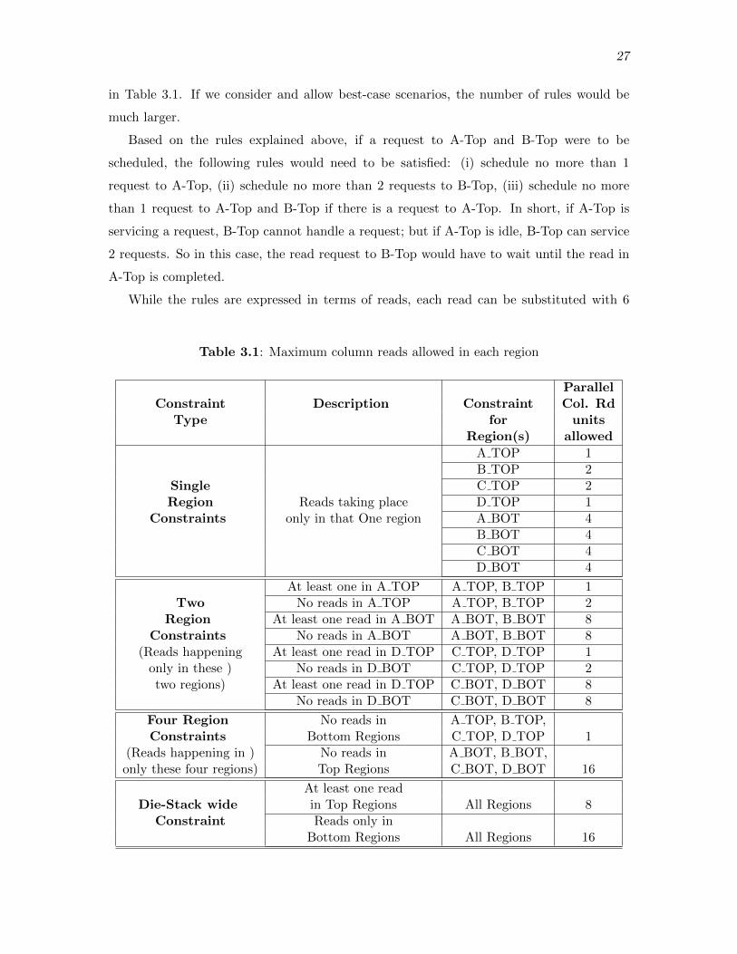
27
in Table 3.1. If we consider and allow best-case scenarios, the number of rules would be
much larger.
Based on the rules explained above, if a request to A-Top and B-Top were to be
scheduled, the following rules would need to be satisfied: (i) schedule no more than 1
request to A-Top, (ii) schedule no more than 2 requests to B-Top, (iii) schedule no more
than 1 request to A-Top and B-Top if there is a request to A-Top. In short, if A-Top is
servicing a request, B-Top cannot handle a request; but if A-Top is idle, B-Top can service
2 requests. So in this case, the read request to B-Top would have to wait until the read in
A-Top is completed.
While the rules are expressed in terms of reads, each read can be substituted with 6
Table 3.1: Maximum column reads allowed in each region
ParallelConstraint Description Constraint Col. Rd
Type for unitsRegion(s) allowed
A TOP 1B TOP 2
Single C TOP 2Region Reads taking place D TOP 1
Constraints only in that One region A BOT 4B BOT 4C BOT 4D BOT 4
At least one in A TOP A TOP, B TOP 1Two No reads in A TOP A TOP, B TOP 2
Region At least one read in A BOT A BOT, B BOT 8Constraints No reads in A BOT A BOT, B BOT 8
(Reads happening At least one read in D TOP C TOP, D TOP 1only in these ) No reads in D BOT C TOP, D TOP 2two regions) At least one read in D TOP C BOT, D BOT 8
No reads in D BOT C BOT, D BOT 8
Four Region No reads in A TOP, B TOP,Constraints Bottom Regions C TOP, D TOP 1
(Reads happening in ) No reads in A BOT, B BOT,only these four regions) Top Regions C BOT, D BOT 16
At least one readDie-Stack wide in Top Regions All Regions 8
Constraint Reads only inBottom Regions All Regions 16
28
precharges, or 2 activates, or 1 write.
Note that a conventional simple memory controller is unaware of IR-drop and regions.
Such a memory controller would disallow 2 parallel reads because in the worst case, both
reads may be destined for A-Top, thus causing an IR-drop violation. Such a naive baseline
will have very poor performance and is not considered further in this study. Our baseline
model adopts the novel constraints we introduce in Table 3.1. In the next section, we
introduce additional mechanisms to improve the memory device’s throughput.
3.4.6 Future DRAM Generations
A DDR3 DRAM chip cannot activate more than 4 banks in a chip within a time period
specified by tFAW. The reason for this is that the Wordlines on the chip need to be driven by
a voltage greater than the supply voltage of the chip. By over-driving the Access Transistors
on the word lines, the sense-amps are able to see the true voltage that is present on cell
capacitors. This increased voltage (VPP ) is provided by charge pumps which are present
on the chip. Performing successive activates depletes these charge pumps, following which
they need time to recover. Doing no more than 4 activates within a window of tFAW ns
ensures that the output of the charge pumps stays within the required voltage.
Future generations of DRAM like DDR4 have VPP (2.5 V) [52] supplied externally,
hence replacing internal charge pumps [53]. By doing this, an 8Gb DDR4 device is able
to lower its tFAW to as low as 20 ns [54], with the eventual goal of eliminating the tFAW
constraint [55] altogether.
As described in Section 3.4.3, IR-drop worsens when the activity on the chip increases.
The DRAM design described in this chapter tries to stay faithful to today’s DDR3 design
as much as possible. We conservatively assume that just like DDR3 DRAM, the dies on the
3D-stack will also be subjected to the tFAW constraint. If the tFAW constraint is indeed
reduced or eliminated in the future, the IR-drop problem reported in this chapter becomes
even greater because of the increased activity.
3.5 Overcoming the Constraints Imposed by IR-drop
In the previous section, we showed that IR-drop imposes new and severe constraints on
device activity. A naive memory controller would not allow more than 1 read or 2 activates
at a time on the device. We therefore introduced a smarter memory controller that is
IR-drop-aware and obeys the 20 rules we introduce in Table 3.1 to support higher activity
levels on the memory device. However, even this smarter memory controller is restrictive
29
and falls well short of the performance of an unconstrained memory device. This section
introduces additional optimizations to bridge this gap.
3.5.1 Handling Throughput Oscillations
According to the rules in Table 3.1, some regions can support higher levels of activity
than others. As a result, some pathological situations can arise that lead to starvation and
lower throughput. Consider the following example that is based on the rules defined in
Table 3.1.
If there exists a read in the top regions, the bottom regions can support at most 7 reads.
However, if there are no reads in the top regions, the bottom regions can support 16 reads.
If the bottom regions are currently handling (say) 10 reads, the scheduler can safely issue
reads to the bottom region, but not to the top region. As a result, the requests to the
top region can get starved. Eventually, every thread will be waiting on a pending memory
request to the top region. At this time, the requests to the top region will be slowly drained
(at the rate of 1 or 2 reads at a time). During this drain, there are no other pending requests
to the bottom regions, so they remain idle. This leads to long stall times for every thread
and memory bandwidth underutilization.
Instead, it is more effective to be in a steady state where the top regions are dealing
with 1 request, while the bottom regions are dealing with 8 requests. While the threads
waiting for the top region are stalled briefly, other threads continue to make progress in
the meantime. This yields a higher aggregate throughput than the default design that
frequently oscillates between high and low throughput phases.
To prevent such oscillations, we prioritize any request that is older than P times the
average read latency. This pushes the scheduler to a steady state where the top regions are
constantly draining 1 or 2 requests while the bottom regions are draining up to 8 requests.
We empirically determined that performance is optimized when P has a value 1.2.
3.5.2 Smart Page Placement
Some regions can drain requests at a faster rate than others and therefore yield much
lower queuing delays and memory access latencies. To optimize throughput, most memory
requests should be steered towards these regions that are more immune to IR-drop viola-
tions. This can be achieved with OS policies that carefully select the regions where pages
are placed.
To estimate the potential for improvement, we first implement a profile-based oracular
scheme. Our benchmarks are profiled for 2 million DRAM accesses. The pages are sorted
30
according to access count and split into 8 sections. Starting with the most accessed section,
they are mapped to A Bot,B Bot,C Bot, D Bot, C Top, B Top, D Top, A Top, in that
order. The benchmarks are simulated again with these page-to-region assignments.
In a realistic implementation, page activities must be tracked at the memory controller
or on the logic die of the 3D-stack. Page activities from the recent past must dictate
page migrations and page placements in the future. We assume that the base layer of the
3D-stack keeps track of all pages touched in the last epoch (a predefined time interval). For
these touched pages, we track the average queuing delay for the blocks in that page. Pages
with the highest queuing delays are moved from the top regions to the bottom regions.
Note that access count in the last epoch is not an effective metric. If an application’s
critical pages are placed in the top region, the core will be starved and it will register few
page accesses in any epoch. This is why we use queuing delay to identify pages that are
introducing the most stall cycles. Any page that has an average queuing delay greater than
Hot Page Migration Threshold(HMT) × Average queuing Delay is migrated to the Bottom
regions.
The metric for demotion of cool pages to the Top regions is the number of page accesses in
the last epoch. Any page that has less than Cold Page Migration Threshold(CMT) number
of page accesses in the last epoch is migrated to the Top regions.
Pages which are not candidates for migration to Top or Bottom regions are not moved.
At the end of every epoch, the DRAM stack is unresponsive to the Central Processing Unit
(CPU) for Migration Penalty number of cycles, similar to a Refresh cycle. All migrations
happen during this window. The Hot-Page and Cold-Page migration thresholds are dynam-
ically modified such that all the migrations can happen within Migration Penalty number
of cycles.
HMT is initialized to 1.2 and CMT is initialized to 0, such that during the initial
epoch, there are many page migrations. If the number of migrations is more than can
be accommodated in the penalty window, then HMT is incremented by 0.05 and CMT is
decremented by 1. A negative value for CMT means that no pages are demoted. However,
if the number of migrations are less than can be handled in the penalty window, then HMT
is decremented by 0.05 and CMT is incremented by 1.
We assume an epoch length of 15 M cycles. After every epoch, the DRAM system incurs
a Migration-Penalty of 10K cycles (an overhead of less than 0.1%). If a shorter epoch is
used, then a large portion of the pages in the Bottom area go untouched, potentially yielding
unwanted migrations to Top regions. We observe that after an initial warm up period, the
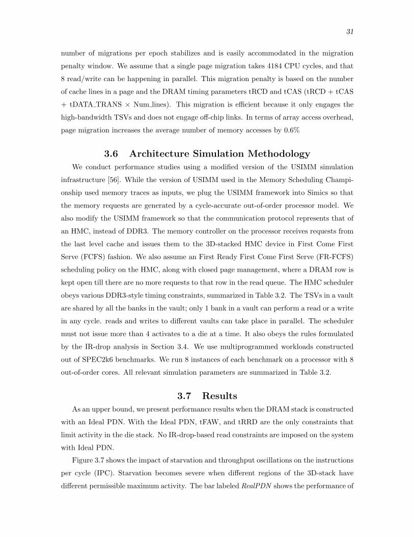
31
number of migrations per epoch stabilizes and is easily accommodated in the migration
penalty window. We assume that a single page migration takes 4184 CPU cycles, and that
8 read/write can be happening in parallel. This migration penalty is based on the number
of cache lines in a page and the DRAM timing parameters tRCD and tCAS (tRCD + tCAS
+ tDATA TRANS × Num lines). This migration is efficient because it only engages the
high-bandwidth TSVs and does not engage off-chip links. In terms of array access overhead,
page migration increases the average number of memory accesses by 0.6%
3.6 Architecture Simulation Methodology
We conduct performance studies using a modified version of the USIMM simulation
infrastructure [56]. While the version of USIMM used in the Memory Scheduling Champi-
onship used memory traces as inputs, we plug the USIMM framework into Simics so that
the memory requests are generated by a cycle-accurate out-of-order processor model. We
also modify the USIMM framework so that the communication protocol represents that of
an HMC, instead of DDR3. The memory controller on the processor receives requests from
the last level cache and issues them to the 3D-stacked HMC device in First Come First
Serve (FCFS) fashion. We also assume an First Ready First Come First Serve (FR-FCFS)
scheduling policy on the HMC, along with closed page management, where a DRAM row is
kept open till there are no more requests to that row in the read queue. The HMC scheduler
obeys various DDR3-style timing constraints, summarized in Table 3.2. The TSVs in a vault
are shared by all the banks in the vault; only 1 bank in a vault can perform a read or a write
in any cycle. reads and writes to different vaults can take place in parallel. The scheduler
must not issue more than 4 activates to a die at a time. It also obeys the rules formulated
by the IR-drop analysis in Section 3.4. We use multiprogrammed workloads constructed
out of SPEC2k6 benchmarks. We run 8 instances of each benchmark on a processor with 8
out-of-order cores. All relevant simulation parameters are summarized in Table 3.2.
3.7 Results
As an upper bound, we present performance results when the DRAM stack is constructed
with an Ideal PDN. With the Ideal PDN, tFAW, and tRRD are the only constraints that
limit activity in the die stack. No IR-drop-based read constraints are imposed on the system
with Ideal PDN.
Figure 3.7 shows the impact of starvation and throughput oscillations on the instructions
per cycle (IPC). Starvation becomes severe when different regions of the 3D-stack have
different permissible maximum activity. The bar labeled RealPDN shows the performance of
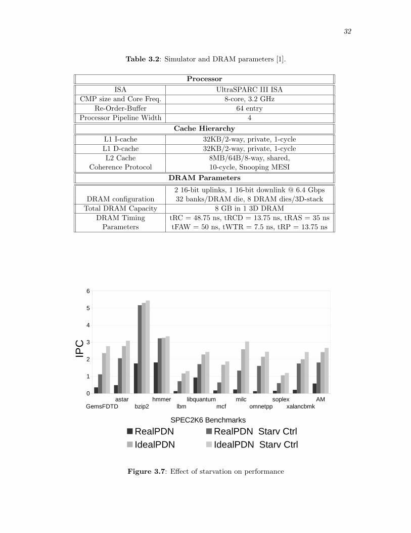
32
Table 3.2: Simulator and DRAM parameters [1].
Processor
ISA UltraSPARC III ISA
CMP size and Core Freq. 8-core, 3.2 GHz
Re-Order-Buffer 64 entry
Processor Pipeline Width 4
Cache Hierarchy
L1 I-cache 32KB/2-way, private, 1-cycle
L1 D-cache 32KB/2-way, private, 1-cycle
L2 Cache 8MB/64B/8-way, shared,Coherence Protocol 10-cycle, Snooping MESI
DRAM Parameters
2 16-bit uplinks, 1 16-bit downlink @ 6.4 GbpsDRAM configuration 32 banks/DRAM die, 8 DRAM dies/3D-stack
Total DRAM Capacity 8 GB in 1 3D DRAM
DRAM Timing tRC = 48.75 ns, tRCD = 13.75 ns, tRAS = 35 nsParameters tFAW = 50 ns, tWTR = 7.5 ns, tRP = 13.75 ns
GemsFDTDastar
bzip2hmmer
lbmlibquantum
mcfmilc
omnetppsoplex
xalancbmkAM
0
1
2
3
4
5
6
RealPDN RealPDN Starv Ctrl
IdealPDN IdealPDN Starv Ctrl
SPEC2K6 Benchmarks
IPC
Figure 3.7: Effect of starvation on performance
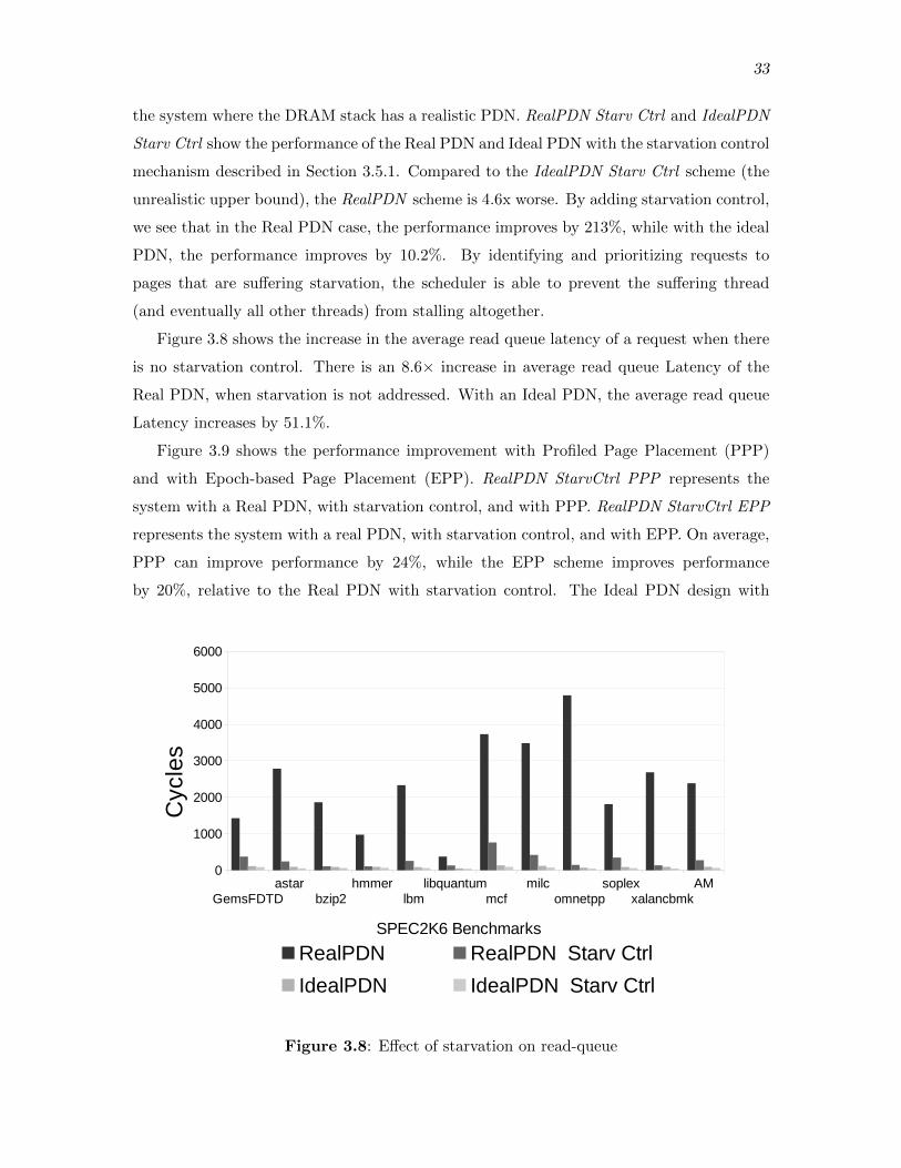
33
the system where the DRAM stack has a realistic PDN. RealPDN Starv Ctrl and IdealPDN
Starv Ctrl show the performance of the Real PDN and Ideal PDN with the starvation control
mechanism described in Section 3.5.1. Compared to the IdealPDN Starv Ctrl scheme (the
unrealistic upper bound), the RealPDN scheme is 4.6x worse. By adding starvation control,
we see that in the Real PDN case, the performance improves by 213%, while with the ideal
PDN, the performance improves by 10.2%. By identifying and prioritizing requests to
pages that are suffering starvation, the scheduler is able to prevent the suffering thread
(and eventually all other threads) from stalling altogether.
Figure 3.8 shows the increase in the average read queue latency of a request when there
is no starvation control. There is an 8.6× increase in average read queue Latency of the
Real PDN, when starvation is not addressed. With an Ideal PDN, the average read queue
Latency increases by 51.1%.
Figure 3.9 shows the performance improvement with Profiled Page Placement (PPP)
and with Epoch-based Page Placement (EPP). RealPDN StarvCtrl PPP represents the
system with a Real PDN, with starvation control, and with PPP. RealPDN StarvCtrl EPP
represents the system with a real PDN, with starvation control, and with EPP. On average,
PPP can improve performance by 24%, while the EPP scheme improves performance
by 20%, relative to the Real PDN with starvation control. The Ideal PDN design with
GemsFDTDastar
bzip2hmmer
lbmlibquantum
mcfmilc
omnetppsoplex
xalancbmkAM
0
1000
2000
3000
4000
5000
6000
RealPDN RealPDN Starv Ctrl
IdealPDN IdealPDN Starv Ctrl
SPEC2K6 Benchmarks
Cyc
les
Figure 3.8: Effect of starvation on read-queue
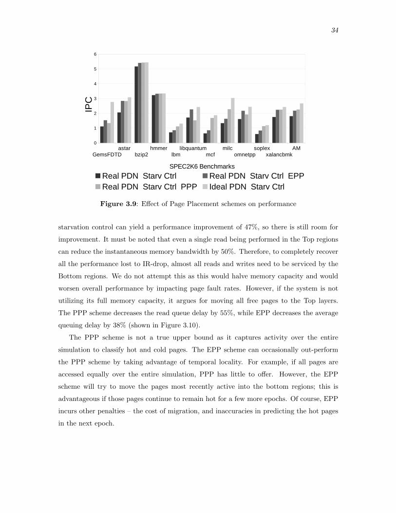
34
GemsFDTDastar
bzip2hmmer
lbmlibquantum
mcfmilc
omnetppsoplex
xalancbmkAM
0
1
2
3
4
5
6
Real PDN Starv Ctrl Real PDN Starv Ctrl EPPReal PDN Starv Ctrl PPP Ideal PDN Starv Ctrl
SPEC2K6 Benchmarks
IPC
Figure 3.9: Effect of Page Placement schemes on performance
starvation control can yield a performance improvement of 47%, so there is still room for
improvement. It must be noted that even a single read being performed in the Top regions
can reduce the instantaneous memory bandwidth by 50%. Therefore, to completely recover
all the performance lost to IR-drop, almost all reads and writes need to be serviced by the
Bottom regions. We do not attempt this as this would halve memory capacity and would
worsen overall performance by impacting page fault rates. However, if the system is not
utilizing its full memory capacity, it argues for moving all free pages to the Top layers.
The PPP scheme decreases the read queue delay by 55%, while EPP decreases the average
queuing delay by 38% (shown in Figure 3.10).
The PPP scheme is not a true upper bound as it captures activity over the entire
simulation to classify hot and cold pages. The EPP scheme can occasionally out-perform
the PPP scheme by taking advantage of temporal locality. For example, if all pages are
accessed equally over the entire simulation, PPP has little to offer. However, the EPP
scheme will try to move the pages most recently active into the bottom regions; this is
advantageous if those pages continue to remain hot for a few more epochs. Of course, EPP
incurs other penalties – the cost of migration, and inaccuracies in predicting the hot pages
in the next epoch.
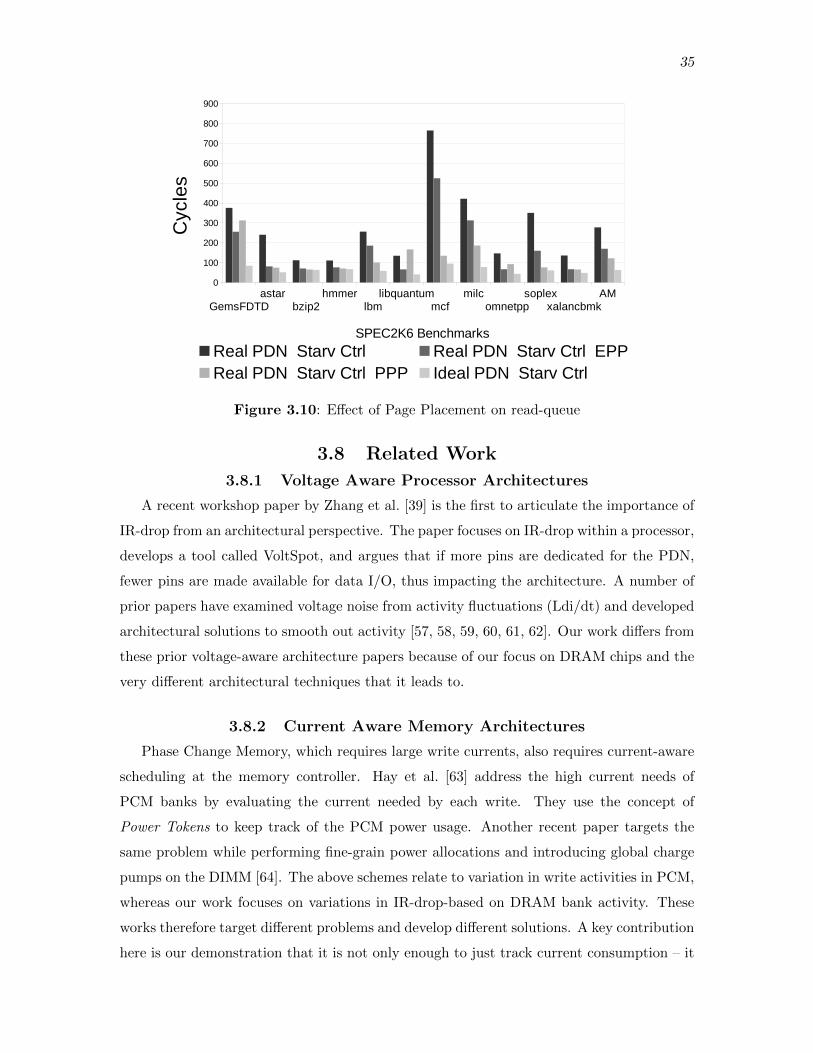
35
GemsFDTDastar
bzip2hmmer
lbmlibquantum
mcfmilc
omnetppsoplex
xalancbmkAM
0
100
200
300
400
500
600
700
800
900
Real PDN Starv Ctrl Real PDN Starv Ctrl EPPReal PDN Starv Ctrl PPP Ideal PDN Starv Ctrl
SPEC2K6 Benchmarks
Cyc
les
Figure 3.10: Effect of Page Placement on read-queue
3.8 Related Work
3.8.1 Voltage Aware Processor Architectures
A recent workshop paper by Zhang et al. [39] is the first to articulate the importance of
IR-drop from an architectural perspective. The paper focuses on IR-drop within a processor,
develops a tool called VoltSpot, and argues that if more pins are dedicated for the PDN,
fewer pins are made available for data I/O, thus impacting the architecture. A number of
prior papers have examined voltage noise from activity fluctuations (Ldi/dt) and developed
architectural solutions to smooth out activity [57, 58, 59, 60, 61, 62]. Our work differs from
these prior voltage-aware architecture papers because of our focus on DRAM chips and the
very different architectural techniques that it leads to.
3.8.2 Current Aware Memory Architectures
Phase Change Memory, which requires large write currents, also requires current-aware
scheduling at the memory controller. Hay et al. [63] address the high current needs of
PCM banks by evaluating the current needed by each write. They use the concept of
Power Tokens to keep track of the PCM power usage. Another recent paper targets the
same problem while performing fine-grain power allocations and introducing global charge
pumps on the DIMM [64]. The above schemes relate to variation in write activities in PCM,
whereas our work focuses on variations in IR-drop-based on DRAM bank activity. These
works therefore target different problems and develop different solutions. A key contribution
here is our demonstration that it is not only enough to just track current consumption – it
36
is also important to track where current is being consumed. Depending on which banks are
currently active, it may or may not be possible to consume more current. Kim et al. [65]
address the tFAW constraint in DRAM stacked over the processor by dynamically allocating
activates to every memory channel connected to a particular DRAM die.
3.8.3 Page Placement
Many prior works have influenced page placement in the memory hierarchy to handle
NUCA latencies [66, 67], NUMA latencies [68, 69, 70], conflict misses in caches [71], DRAM
power modes [72], DRAM/PCM hybrids [73, 74], etc. Our work borrows the key ideas
in these techniques and shows that they can be highly effective to address the emerging
IR-drop problem.
3.8.4 Circuit Efforts to Reduce IR-drop.
Wu et al. [46] study the impact of a stacked processor-DRAM device on power delivery
and propose using Decaps on the DRAM layer to reduce dynamic IR-drop. Kang et al. [31]
suggest the addition of TSVs to provide more power/ground lines. While they foresee only
a modest area overhead of 0.5%, the package routing and extra package pins required to
accomplish this will increase cost. Healy et al. [41] compare the power supply noise caused
by different power TSV topologies. Their results suggest the use of a topology where the
Power/Ground TSVs are spread evenly rather than clustered over the Power/Ground C4
bumps. Jung et al. [42] illustrate that higher TSV counts can increase routing congestion
because power/ground TSVs can be larger than standard cells, thus exacerbating IR-drop
issues. They propose power consumption aware TSV placement.
3.9 Conclusions
In this work, we highlight an emerging important problem. We show that while 2D
DRAM chips are rarely exposed to IR-drop violations, 3D-stacked memory devices can
be highly prone to such violations. For acceptable performance, the memory controller
must encode a number of rules to handle the nonuniform vulnerability of each bank to
IR-drop. We show that even such a smart memory controller falls short of the performance
of an unconstrained memory device by 4.6×. A large fraction of this gap is bridged by
introducing a smarter scheduler and a page migration mechanism. The starvation-aware
scheduler brings the gap to 1.47×. By further adding page migration, the gap is brought
to 1.2×. We thus show that effective architectural policies can yield high performance at
low pin/TSV counts.
37
Several future technology parameters are currently unknown and it is not clear how
commercial designs will cope with IR-drop constraints. Our work shows that architectural
policies can represent an important approach, possibly mitigating the need for some costly
approaches.
Our work can be extended in many different ways. For example, our IR-drop analysis
can be extended to handle Refresh, and more sophisticated schedulers can be designed to
bridge the 1.2× performance gap. While more scheduling rules can improve performance,
they also increase power, area, and design complexity. The definition of an optimal memory
controller remains an open problem.
CHAPTER 4
ADDRESSING PEAK CURRENT
PROBLEMS IN MULTIRANKED
DRAM
The charge stored in DRAM cells leaks over time and needs to be refreshed periodically.
There are two reasons why DRAM refresh will be a critical bottleneck in high capacity
memory systems. First, as the size of the DRAM chip grows, so does the time spent in
refreshing all the cells. Second, DRAM refresh is a very current intensive process. If all
the ranks in a system were to refresh at the same time, the current consumed for that
duration would be much higher than the current consumed during normal operation. Since
the power and cooling systems are designed to accommodate peak power ratings, higher
peak power consumption directly leads to higher cost. To avoid this, server manufacturers
do not refresh all ranks simultaneously. Instead, they stagger refreshes, thus leading to
lower peak current/power consumption. While staggering avoids the peak power problem,
it increases the performance impact of refresh.
As refresh latencies increase, the performance loss due to staggered refresh will also
increase. This chapter analyzes the reasons for the performance loss from staggered refresh
and proposes solutions for the same. Our analysis also shows that write drains in high
capacity memory systems built with Nonvolatile Memories (NVM) have similar character-
istics to DRAM refresh; both result in certain ranks being unavailable for some time. In
Section 4.7.4, we show that the solutions proposed in this chapter for DRAM refresh are
also applicable to reducing the performance overheads associated with long latency NVM
writes. The chapter therefore makes a contribution that will be useful to two segments that
will drive the high capacity memory market share in the coming decade.
4.1 DRAM Refresh
DRAM technology is expected to scale for another generation or two [75] and will be
used widely in most systems for at least another decade. In addition, DRAM vendors will
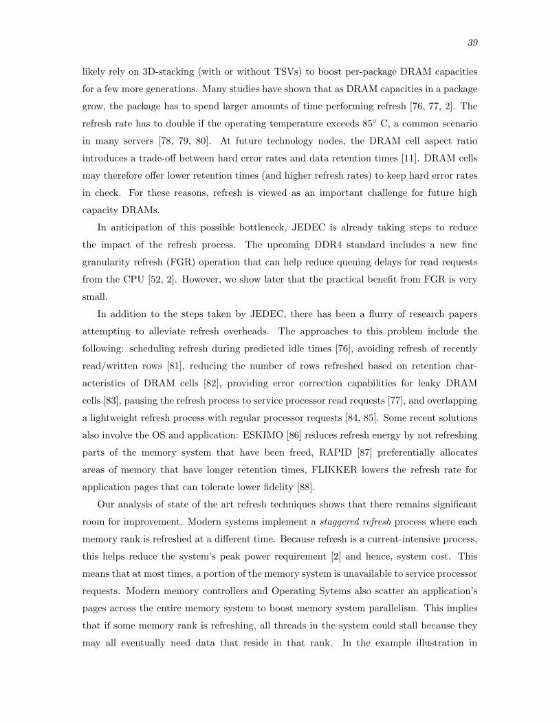
39
likely rely on 3D-stacking (with or without TSVs) to boost per-package DRAM capacities
for a few more generations. Many studies have shown that as DRAM capacities in a package
grow, the package has to spend larger amounts of time performing refresh [76, 77, 2]. The
refresh rate has to double if the operating temperature exceeds 85 C, a common scenario
in many servers [78, 79, 80]. At future technology nodes, the DRAM cell aspect ratio
introduces a trade-off between hard error rates and data retention times [11]. DRAM cells
may therefore offer lower retention times (and higher refresh rates) to keep hard error rates
in check. For these reasons, refresh is viewed as an important challenge for future high
capacity DRAMs.
In anticipation of this possible bottleneck, JEDEC is already taking steps to reduce
the impact of the refresh process. The upcoming DDR4 standard includes a new fine
granularity refresh (FGR) operation that can help reduce queuing delays for read requests
from the CPU [52, 2]. However, we show later that the practical benefit from FGR is very
small.
In addition to the steps taken by JEDEC, there has been a flurry of research papers
attempting to alleviate refresh overheads. The approaches to this problem include the
following: scheduling refresh during predicted idle times [76], avoiding refresh of recently
read/written rows [81], reducing the number of rows refreshed based on retention char-
acteristics of DRAM cells [82], providing error correction capabilities for leaky DRAM
cells [83], pausing the refresh process to service processor read requests [77], and overlapping
a lightweight refresh process with regular processor requests [84, 85]. Some recent solutions
also involve the OS and application: ESKIMO [86] reduces refresh energy by not refreshing
parts of the memory system that have been freed, RAPID [87] preferentially allocates
areas of memory that have longer retention times, FLIKKER lowers the refresh rate for
application pages that can tolerate lower fidelity [88].
Our analysis of state of the art refresh techniques shows that there remains significant
room for improvement. Modern systems implement a staggered refresh process where each
memory rank is refreshed at a different time. Because refresh is a current-intensive process,
this helps reduce the system’s peak power requirement [2] and hence, system cost. This
means that at most times, a portion of the memory system is unavailable to service processor
requests. Modern memory controllers and Operating Sytems also scatter an application’s
pages across the entire memory system to boost memory system parallelism. This implies
that if some memory rank is refreshing, all threads in the system could stall because they
may all eventually need data that reside in that rank. In the example illustration in
40
Refresh to Rank 1
T1R2
Time
Rank 2 available
Rank 3 available
T2R3
T1R1
T2R2
T2R1
T3R1
Refresh to Rank 2
T1R1
Rank 1 available
Rank 3 available
T2R2
T1R3
T1R2
T3R3
T3R2
Thread 1 reads from Rank 2
Thread 1 stalled on Rank 1
Successful and unsuccessful accesses, with a baseline page allocation policy.Threads T1, T2, and T3 uniformly touch all the ranks.
T2R2
T2R2
T2R2
T1R1
T3R3
T1R1
T2R2
T1R1
T1R1
T3R3
T3R3
Successful and unsuccessful accesses, with a colored refresh page allocation policy.Thread T1 only touches rank R1, T2 only touches R2, T3 only touches R3.
T2R2
T3R3
T1R1
Figure 4.1: Stalls with baseline and rank assignment policies.
Figure 4.1, a refresh to rank 1 stalls threads T1, T2, and T3 in the baseline. The combination
of staggered refresh and page scattering results in a 25.1% increase in execution time over
an idealized system with no refresh penalty (assuming 2 channels, 2 ranks per channel and
32 Gb chips at high temperature). State of the art hardware-intensive refresh techniques
are able to yield an execution time reduction of at most 4.1%, relative to this baseline.
We also examine the write bottleneck in future NVMs. Multiple nonvolatile cell technolo-
gies (e.g., PCM and Memristors) are expected to soon be mainstream. Both technologies
suffer from long write latencies of several hundred nanoseconds [89, 90, 91, 92]. Typically,
memory controllers defer writes and perform writes in bursts that can occupy the memory
channel and the corresponding banks for many hundreds of cycles. Several recent papers
have therefore attempted to optimize the write process in NVMs [90, 91, 92, 93, 94]. Similar
to refresh, write drains are performed for a rank at a time. In NVMs, the data transfers
on the channel take tens of nanoseconds, while the actual writes in the memory chips take
hundreds of nanoseconds. A burst of writes is therefore quickly sent on the channel to 1
rank, and while that rank performs writes in its banks in the background, the memory
controller switches to servicing reads from other ranks on the same channel. Similar to the
41
refresh process, the regions of memory performing writes are unavailable for a long time,
potentially causing stalls in all threads.
We design a simple solution, Rank Assignment, that can be implemented entirely in the
OS page allocator and that is more effective than state of the art hardware schemes that
target service interruptions from refreshes and write drains. In the baseline described above,
a single rank’s refresh or write drain can stall every thread in the system. To prevent this,
the OS allocates pages such that pages from 1 thread are assigned to the fewest number
of ranks (ideally just 1 rank). This thread is only stalled when its rank is refreshing or
draining writes.
In Figure 4.1, a refresh to rank 1 only stalls thread T1 when using the rank assignment
page allocator. While other ranks are refreshing, this thread may even see a performance
boost because of lower contention for the shared memory channel. The proposed page
allocator therefore isolates the negative impact of refresh and write drains to a single thread
while accelerating other threads assigned to that channel.
Traditionally, the OS and memory controller have adopted policies that spread requests
from a thread across the entire memory system. We show that such policies must be
questioned in the modern era and that it is better to colocate an application’s pages in a
single rank. We further show that even an approximate mapping of pages to ranks is highly
beneficial, thus lowering the burden on the OS.
The downside of this approach is that a thread cannot exploit rank-level parallelism; this
has a very small performance penalty in the future because DDR4 provides high bank-level
parallelism (16 banks per rank) [95].
Compared to the best competing hardware approach, rank assignment yields an exe-
cution time that is 15% lower, while requiring no changes to the memory controller, DDR
standard, and memory chips.
4.2 Background
4.2.1 DRAM Basics
A modern high performance processor typically has up to 4 DDR3 memory controllers
(MC). Each MC controls 1 64-bit wide DDR3 channel and the 1-2 DIMMs connected to
that channel. A DIMM has 1-4 ranks. Each rank consists of a collection of DRAM chips
that together have an output width of 64 bits. A 64-byte cache line is fetched from a single
rank with 8 64-bit transfers (a burst of 8). A rank is composed of 8 independent banks in
DDR3 and 16 banks in DDR4. Thus, a single channel can support multiple ranks and tens
of banks, i.e., a high amount of memory system parallelism.
42
A single activate command to a bank brings an entire row into a row buffer. Cache
lines are read from or written to this row with column-reads or column-writes. The bank
must be precharged before a new row can be fetched into the row buffer. The memory
controller schedules these commands to all the banks while carefully satisfying all timing
constraints. The scheduler does several things to maximize performance: looking for row
buffer hits, precharging banks early, maintaining fairness across threads, prioritizing reads,
etc. Typically, multiple banks are in various stages of a data block access at a time, but all
cache line transfers are eventually serialized on the shared channel.
4.2.2 Retention Time and Refresh Interval
The charge on a DRAM cell weakens over time. The DDR standard requires every cell
to be refreshed within a 64 ms interval, referred to as the retention time. At temperatures
higher than 85 C (referred to as Extended Temperature range), the retention time is halved
to 32 ms to account for the higher leakage rate. The refresh of the entire memory system
is partitioned into 8,192 smaller refresh operations. One such refresh operation has to be
issued every 7.8 µs (64 ms/8192). This 7.8 µs interval is referred to as the refresh interval,
tREFI. The DDR3 standard requires that 8 refresh operations be issued within a time
window equal to 8×tREFI, giving the memory controller some flexibility when scheduling
these refresh operations. Refresh operations are issued at rank granularity in DDR3 and
DDR4.
We next describe the internals of the refresh operation in some detail. These details are
not pertinent to the proposals in this chapter since we do not modify the DRAM chip or
refresh protocol in any way. However, we provide a detailed description here because these
details are relevant when modeling competing schemes, and it helps explain the inherent
challenges in hardware-based approaches to the refresh problem.
4.2.3 Refresh Cycle Time and Recovery time
Upon receiving a refresh command, the DRAM chips enter a refresh mode that has
been carefully designed to perform the maximum amount of cell refresh in as little time as
possible. During this time, the current carrying capabilities of the power delivery network
and the charge pumps are stretched to the limit. The operation lasts for a time referred to
as the refresh cycle time, tRFC. Towards the end of this period, the refresh process starts to
wind down and some recovery time is provisioned so that the banks can be precharged and
charge is restored to the charge pumps. Providing this recovery time at the end allows the
memory controller to resume normal operation at the end of tRFC. Without this recovery
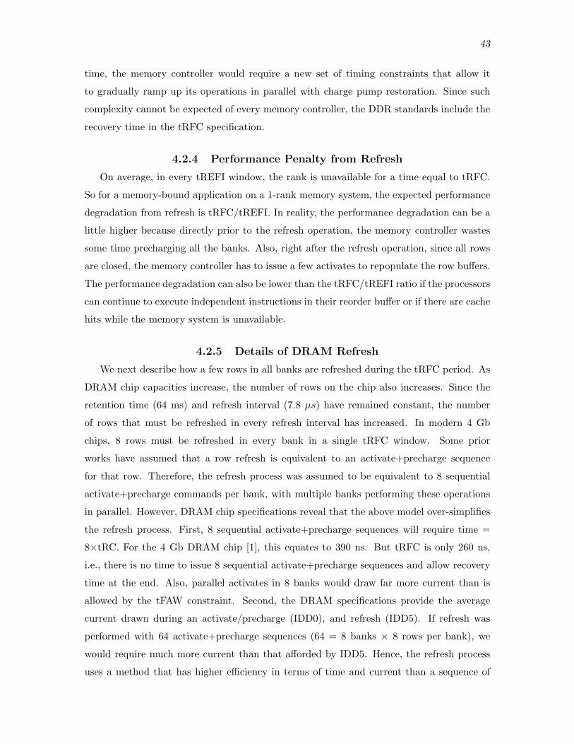
43
time, the memory controller would require a new set of timing constraints that allow it
to gradually ramp up its operations in parallel with charge pump restoration. Since such
complexity cannot be expected of every memory controller, the DDR standards include the
recovery time in the tRFC specification.
4.2.4 Performance Penalty from Refresh
On average, in every tREFI window, the rank is unavailable for a time equal to tRFC.
So for a memory-bound application on a 1-rank memory system, the expected performance
degradation from refresh is tRFC/tREFI. In reality, the performance degradation can be a
little higher because directly prior to the refresh operation, the memory controller wastes
some time precharging all the banks. Also, right after the refresh operation, since all rows
are closed, the memory controller has to issue a few activates to repopulate the row buffers.
The performance degradation can also be lower than the tRFC/tREFI ratio if the processors
can continue to execute independent instructions in their reorder buffer or if there are cache
hits while the memory system is unavailable.
4.2.5 Details of DRAM Refresh
We next describe how a few rows in all banks are refreshed during the tRFC period. As
DRAM chip capacities increase, the number of rows on the chip also increases. Since the
retention time (64 ms) and refresh interval (7.8 µs) have remained constant, the number
of rows that must be refreshed in every refresh interval has increased. In modern 4 Gb
chips, 8 rows must be refreshed in every bank in a single tRFC window. Some prior
works have assumed that a row refresh is equivalent to an activate+precharge sequence
for that row. Therefore, the refresh process was assumed to be equivalent to 8 sequential
activate+precharge commands per bank, with multiple banks performing these operations
in parallel. However, DRAM chip specifications reveal that the above model over-simplifies
the refresh process. First, 8 sequential activate+precharge sequences will require time =
8×tRC. For the 4 Gb DRAM chip [1], this equates to 390 ns. But tRFC is only 260 ns,
i.e., there is no time to issue 8 sequential activate+precharge sequences and allow recovery
time at the end. Also, parallel activates in 8 banks would draw far more current than is
allowed by the tFAW constraint. Second, the DRAM specifications provide the average
current drawn during an activate/precharge (IDD0), and refresh (IDD5). If refresh was
performed with 64 activate+precharge sequences (64 = 8 banks × 8 rows per bank), we
would require much more current than that afforded by IDD5. Hence, the refresh process
uses a method that has higher efficiency in terms of time and current than a sequence of
44
activate and precharge commands.
This method is based on the high number of subarrays being provisioned in every bank.
For example, a bank may have 16 subarrays, of which only 4 are accessed during a regular
activate operation. This observation also formed the basis for the recent subarray-level
parallelism (SALP) idea of Kim et al. [51]. During a refresh operation, the same row in all
16 subarrays undergo an activation and precharge. In this example, 4 rows worth of data
are being refreshed in parallel within a single bank. Also, the current requirement for this
is not 4x the current for a regular activate; by sharing many of the circuits within the bank,
the current does not increase linearly with the extent of subarray-level parallelism. Thus,
a single bank uses the maximum allowed current draw to perform parallel refresh in a row
in every subarray; each bank is handled sequentially (refreshes in two banks may overlap
slightly based on current profiles), and there is a recovery time at the end.
4.2.6 DRAM Scaling
Refresh overheads are expected to increase dramatically in the future as DRAM chip
capacities increase. Table 4.1 shows this scaling trend [2]. The number of cells that must be
refreshed in every tRFC increases linearly with capacity. Therefore, we also see a roughly
linear increase in tRFC (the exact values would depend on the technology node, the current
limits, and the subarrays that are refreshed in parallel). In future 32 Gb chips, the tRFC
is as high as 640 ns, giving a tRFC/tREFI ratio of 8.2%. At high temperatures, this
ratio doubles to 16.4%. tREFI will also reduce if DRAM cell capacitances reduce in the
future [11]. In a 3D-stacked package, the number of cells increases without a corresponding
increase in pin count and power delivery [96] – this too results in a high tRFC.
Table 4.1: Refresh latencies for high DRAM chip capacities [2].
Chip tRFC tRFC1x tRFC2x tRFC4xCapacity (Gb) (ns) (ns) (ns) (ns)
8 350 350 240 160
16 480 480 350 240
32 640 640 480 350
tREFI 7800 7800 3900 1950
45
4.2.7 Fine Granularity Refresh in DDR4
In response to these high tRFC refresh times, the DDR4 standard introduces fine
granularity refresh (FGR) operations [3]. FGR-1x is the same as the refresh process in
DDR3. FGR-2x partitions each DDR3 refresh operation into 2 smaller operations. In
essence, the tREFI is halved (refresh operations must be issued twice as often), and the
tRFC also reduces (since each refresh operation does half the work). FGR-4x partitions
each DDR3 refresh operation into 4 smaller operations. The tRFC and tREFI for these
modes are also summarized in Table 4.1.
These modes were introduced to reduce wait times for read requests that queue up during
a refresh operation. In general, average queuing delays are reduced when a large refresh
operation is broken into multiple smaller refresh operations. While the early projections of
FGR were optimistic [52], the latest DDR4 parameters [2] reveal that FGR can introduce
high overheads. A single FGR-2x operation has to refresh half the cells refreshed in an
FGR-1x operation, thus potentially requiring half the time. But an FGR-2x operation and
an FGR-1x operation must both incur the same recovery cost at the end to handle depleted
charge pumps. The data in Table 4.1 show that for 32 Gb chips, tRFC for FGR-2x mode
is 480 ns, while tRFC for FGR-1x is 640 ns. The overheads of the recovery time are so
significant that two FGR-2x operations take 50% longer than a single FGR-1x operation.
Similarly, going to FGR-4x mode results in a tRFC of 350 ns. Therefore, four FGR-4x
refresh operations would keep the rank unavailable for 1400 ns, while a single FGR-1x
refresh operation would refresh the same number of cells, but keep the rank unavailable
for only 640 ns. The high refresh recovery overheads in FGR-2x and FGR-4x limit their
effectiveness in reducing queuing delays (see results in Section 4.7.5). Therefore, refresh
remains an important problem.
For example, let us assume that the read queue is empty when a refresh operation begins,
a new read is enqueued every 10 ns, and it takes 10 ns to process each read after the refresh
is completed. If the refresh operation takes 50 ns, the first read arrives at time 10 ns and
is processed at time 50 ns, the second read arrives at time 20 ns and is processed at time
60 ns, and so on. The total queuing delay for the five reads that arrive during refresh =
40+40+40+40+40 = 200 ns. If the refresh operation takes 100 ns, the total queuing delay
for the 10 reads that arrive during refresh = 90×10 = 900 ns. Even though the smaller
50 ns refresh operation has to be performed twice, it results in an accumulated read queuing
delay of only 400 ns, while the longer refresh operation results in a read queuing delay of
900 ns.
46
4.2.8 NVM Writes
We next describe how writes are handled in memory systems. The memory controller
typically prioritizes reads, and arriving writes are buffered in a write queue. When the write
queue reaches a high water mark, the memory controller starts draining writes until the
write queue reaches a low water mark [97]. The memory controller has to introduce a bus
turnaround delay (tWTR) when switching from writes to reads in a given rank. To amortize
this overhead, a number of writes are typically serviced in a rank before switching back to
reads. Typically, memory controllers will drain 16-32 writes at a time to balance queuing
delays for subsequent reads and the bus turnaround overhead. A write queue drain can
therefore take hundreds of nanoseconds. During this write drain to a rank, other ranks on
the channel are available for reads. A short tRTR timing delay (2 cycles) is introduced when
switching between accesses to different ranks. This tRTR delay is incurred regardless of
whether the two ranks are performing reads or writes. Therefore, from a memory throughput
perspective, there is no advantage to co-ordinating the write queue drains of two ranks on
a channel. Similar to refresh, the write queue drain can be viewed as a per-rank operation.
Emerging NVM cells will likely find a place in server memory systems in the near future.
All of the emerging NVM cells suffer from long write latencies. While the tWR delay in
DRAM is 15 ns [1], the same delay in PCM is 125 ns [89], and in Memristors is expected
to range from 200-700 ns. Therefore, a write drain in these NVMs will involve sending tens
of writes to a rank on the memory channel in about a hundred cycles; the banks in the
rank perform the writes in the next many hundred cycles; meanwhile, reads can be issued
to other available banks and ranks sharing that channel. The banks performing the writes
remain unavailable for many hundred cycles.
4.3 Motivation
Having described the basics, we now focus on creating a good baseline and analyzing it.
4.3.1 Peak Power
DRAM refresh is performed at rank granularity. The memory controller can co-ordinate
and issue refresh commands to every rank at the same time (simultaneous refresh) or stagger
them so only 1 rank is refreshing at a time (staggered refresh). Commercial systems prefer
the latter [2] because it limits the peak power of the memory system (since refresh is the
most power-intensive operation performed within DRAM). Even though the average power
consumption remains the same, limiting the peak power reduces system cost. With the
Micron power calculator [98], we estimated that in a single channel with two ranks, with x4
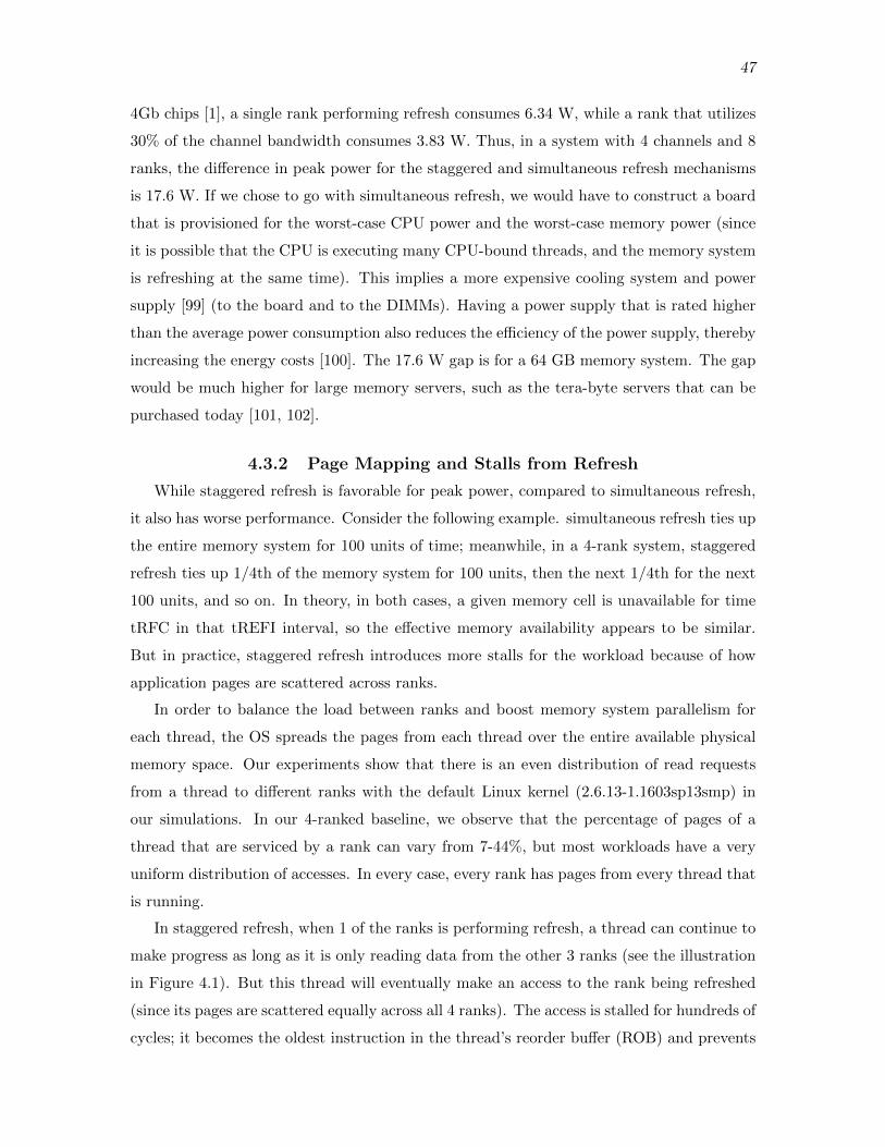
47
4Gb chips [1], a single rank performing refresh consumes 6.34 W, while a rank that utilizes
30% of the channel bandwidth consumes 3.83 W. Thus, in a system with 4 channels and 8
ranks, the difference in peak power for the staggered and simultaneous refresh mechanisms
is 17.6 W. If we chose to go with simultaneous refresh, we would have to construct a board
that is provisioned for the worst-case CPU power and the worst-case memory power (since
it is possible that the CPU is executing many CPU-bound threads, and the memory system
is refreshing at the same time). This implies a more expensive cooling system and power
supply [99] (to the board and to the DIMMs). Having a power supply that is rated higher
than the average power consumption also reduces the efficiency of the power supply, thereby
increasing the energy costs [100]. The 17.6 W gap is for a 64 GB memory system. The gap
would be much higher for large memory servers, such as the tera-byte servers that can be
purchased today [101, 102].
4.3.2 Page Mapping and Stalls from Refresh
While staggered refresh is favorable for peak power, compared to simultaneous refresh,
it also has worse performance. Consider the following example. simultaneous refresh ties up
the entire memory system for 100 units of time; meanwhile, in a 4-rank system, staggered
refresh ties up 1/4th of the memory system for 100 units, then the next 1/4th for the next
100 units, and so on. In theory, in both cases, a given memory cell is unavailable for time
tRFC in that tREFI interval, so the effective memory availability appears to be similar.
But in practice, staggered refresh introduces more stalls for the workload because of how
application pages are scattered across ranks.
In order to balance the load between ranks and boost memory system parallelism for
each thread, the OS spreads the pages from each thread over the entire available physical
memory space. Our experiments show that there is an even distribution of read requests
from a thread to different ranks with the default Linux kernel (2.6.13-1.1603sp13smp) in
our simulations. In our 4-ranked baseline, we observe that the percentage of pages of a
thread that are serviced by a rank can vary from 7-44%, but most workloads have a very
uniform distribution of accesses. In every case, every rank has pages from every thread that
is running.
In staggered refresh, when 1 of the ranks is performing refresh, a thread can continue to
make progress as long as it is only reading data from the other 3 ranks (see the illustration
in Figure 4.1). But this thread will eventually make an access to the rank being refreshed
(since its pages are scattered equally across all 4 ranks). The access is stalled for hundreds of
cycles; it becomes the oldest instruction in the thread’s reorder buffer (ROB) and prevents
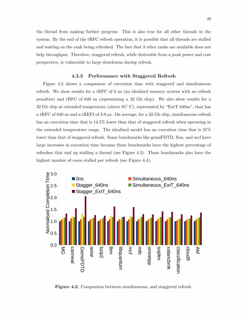
48
the thread from making further progress. This is also true for all other threads in the
system. By the end of the tRFC refresh operation, it is possible that all threads are stalled
and waiting on the rank being refreshed. The fact that 3 other ranks are available does not
help throughput. Therefore, staggered refresh, while desireable from a peak power and cost
perspective, is vulnerable to large slowdowns during refresh.
4.3.3 Performance with Staggered Refresh
Figure 4.2 shows a comparison of execution time with staggered and simultaneous
refresh. We show results for a tRFC of 0 ns (an idealized memory system with no refresh
penalties) and tRFC of 640 ns (representing a 32 Gb chip). We also show results for a
32 Gb chip at extended temperature (above 85 C), represented by “ExtT 640ns”, that has
a tRFC of 640 ns and a tREFI of 3.9 µs. On average, for a 32 Gb chip, simultaneous refresh
has an execution time that is 14.5% lower than that of staggered refresh when operating in
the extended temperature range. The idealized model has an execution time that is 21%
lower than that of staggered refresh. Some benchmarks like gemsFDTD, lbm, and mcf have
large increases in execution time because these benchmarks have the highest percentage of
refreshes that end up stalling a thread (see Figure 4.3). These benchmarks also have the
highest number of cores stalled per refresh (see Figure 4.4).
MG
canne al
Gem
s FD
TD
astar
bzip2
lbm
libquan tum
mcf
milc
omnet pp
soplex
xalanc bmk
classif ication
cloud9
AM
0.0
0.5
1.0
1.5
2.0
2.5
3.00ns Simultaneous_640nsStagger_640ns Simultaneous_ExtT_640nsStagger_ExtT_640ns
Nor
mal
ised
Com
plet
ion
TIm
e
Figure 4.2: Comparison between simultaneous, and staggered refresh.
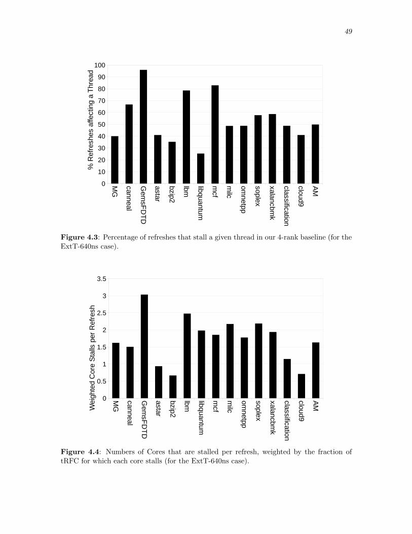
49
MG
canne al
Gem
s FD
TD
astar
bzip2
lbm
libquan tum
mcf
milc
omnet pp
soplex
xalanc bmk
classif ication
cloud9
AM
0
10
20
30
40
50
60
70
80
90
100
% R
efre
shes
affe
ctin
g a
Thr
ead
Figure 4.3: Percentage of refreshes that stall a given thread in our 4-rank baseline (for theExtT-640ns case).
MG
canne al
Gem
s FD
TD
astar
bzip2
lbm
libquan tum
mcf
milc
omnet pp
soplex
xalanc bmk
classif ication
cloud9
AM
0
0.5
1
1.5
2
2.5
3
3.5
Wei
ghte
d C
ore
Sta
lls p
er R
efre
sh
Figure 4.4: Numbers of Cores that are stalled per refresh, weighted by the fraction oftRFC for which each core stalls (for the ExtT-640ns case).
50
Figure 4.3 quantifies the percentage of refresh operations that end up stalling a given
thread in the workload. As discussed earlier, because a thread’s pages are scattered across
all ranks, every refresh operation has the potential to stall every thread. This is observed
in a workload such as GemsFDTD. Across the entire benchmark suite, on average, a thread
is stalled by half the refresh operations in the memory system.
Figure 4.4 quantifies the stalls resulting from a typical refresh operation. The Y-axis
shows the number of cores that were stalled by a single refresh operation, where every core
is weighted by the duration that it was stalled for. For example, if 3 cores were stalled,
each for half the duration of a refresh operation, the weighted core stall time would be 1.5.
While GemsFDTD experiences a weighted core stall time of over 3 (8 is the maximum), on
average, the weighted core stall time is 1.63.
The above discussion helps establish our baseline system – the staggered refresh mecha-
nism that has low peak power and that attributes 21% of its execution time to refresh-related
stalls for 32 Gb at extended temperature. Because of the staggered process, the penalty
from refresh is much higher than the tRFC/tREFI ratio (16%). In theory, for our 4-rank
system, the penalty can be as high as 4×tRFC/tREFI, but as shown by Figures 4.3 and
4.4, in practice not all threads are stalled all the time during every refresh, so the penalty
is lower. The baseline therefore provides a significant room for improvement with smarter
refresh policies. The room for improvement will of course vary based on our assumptions
for refresh. We focus most of our results on the most aggressive DDR4 specification known
to date (32 Gb chip at extended temperature).
4.3.4 Impact of NVM Writes
In Figure 4.5, we show the impact of different write scheduling policies in a system with
PCM main memory, relative to an idealized memory system with no writes. The second
bar (Wr Drain) shows the execution time when write drains are performed with Hi/Lo
water mark of 40/20 writes. The last bar (EqualPriority) shows the execution time when
reads and writes are given equal priorities and are both serviced in FCFS fashion. The
best baseline is 21% worse than the idealized memory system, showing a significant room
for improvement. On average, a write drain process keeps 8.6 banks (out of 16 banks in a
channel) busy, stalling 5.7 of 8 threads on average on every write drain. We also see minor
performance differences (<1% ) by co-ordinating the write drains in the ranks sharing a
channel.
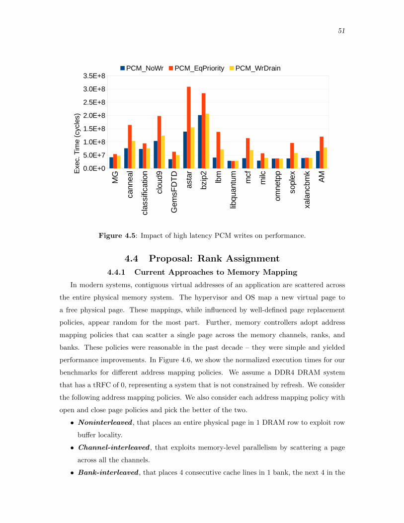
51
MG
cann
eal
clas
sific
atio
n
clou
d9
Gem
sFD
TD
asta
r
bzip
2
lbm
libqu
antu
m
mcf
milc
omne
tpp
sopl
ex
xala
ncbm
k
AM
0.0E+0
5.0E+7
1.0E+8
1.5E+8
2.0E+8
2.5E+8
3.0E+8
3.5E+8PCM_NoWr PCM_EqPriority PCM_WrDrain
Exe
c. T
ime
(cyc
les)
Figure 4.5: Impact of high latency PCM writes on performance.
4.4 Proposal: Rank Assignment
4.4.1 Current Approaches to Memory Mapping
In modern systems, contiguous virtual addresses of an application are scattered across
the entire physical memory system. The hypervisor and OS map a new virtual page to
a free physical page. These mappings, while influenced by well-defined page replacement
policies, appear random for the most part. Further, memory controllers adopt address
mapping policies that can scatter a single page across the memory channels, ranks, and
banks. These policies were reasonable in the past decade – they were simple and yielded
performance improvements. In Figure 4.6, we show the normalized execution times for our
benchmarks for different address mapping policies. We assume a DDR4 DRAM system
that has a tRFC of 0, representing a system that is not constrained by refresh. We consider
the following address mapping policies. We also consider each address mapping policy with
open and close page policies and pick the better of the two.
• Noninterleaved , that places an entire physical page in 1 DRAM row to exploit row
buffer locality.
• Channel-interleaved , that exploits memory-level parallelism by scattering a page
across all the channels.
• Bank-interleaved , that places 4 consecutive cache lines in 1 bank, the next 4 in the
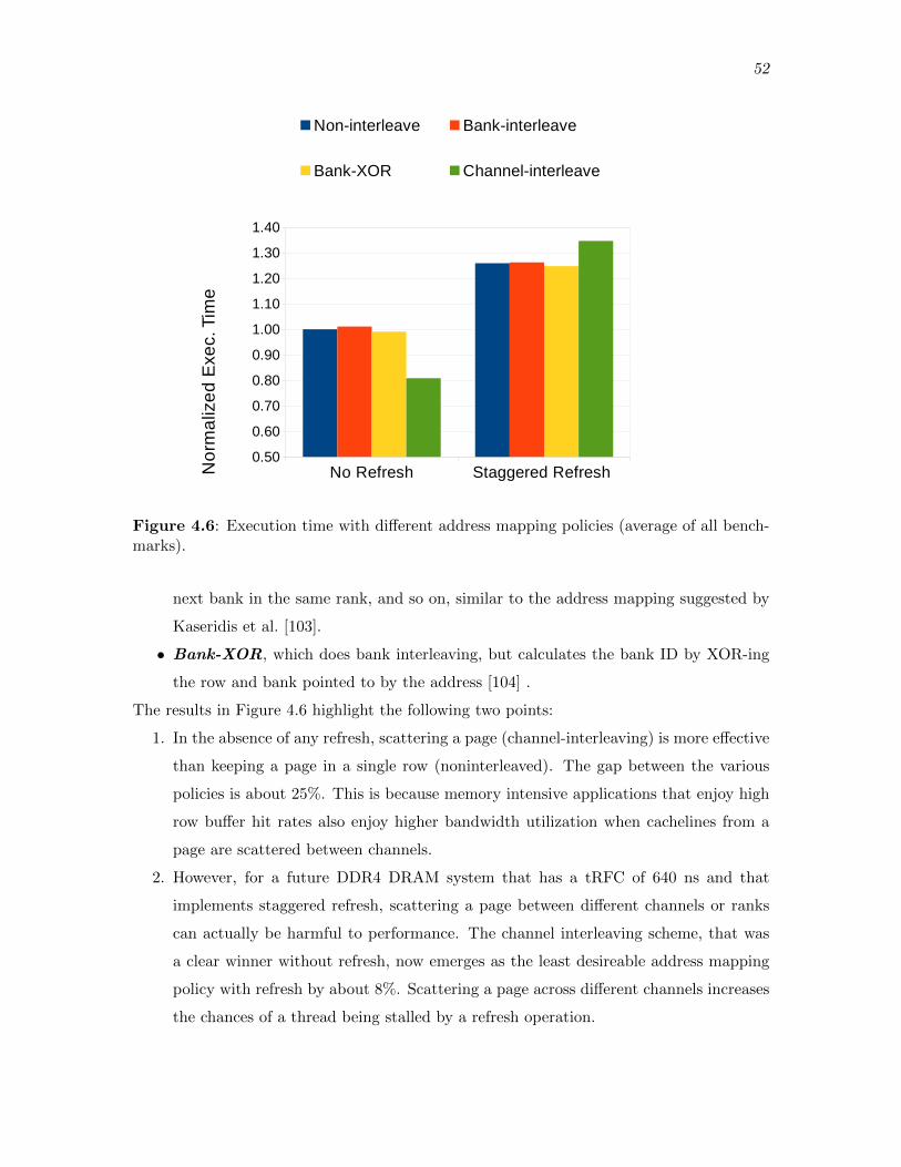
52
No Refresh Staggered Refresh 0.50
0.60
0.70
0.80
0.90
1.00
1.10
1.20
1.30
1.40
Non-interleave Bank-interleave
Bank-XOR Channel-interleave
No
rma
lize
d E
xec.
Tim
e
Figure 4.6: Execution time with different address mapping policies (average of all bench-marks).
next bank in the same rank, and so on, similar to the address mapping suggested by
Kaseridis et al. [103].
• Bank-XOR, which does bank interleaving, but calculates the bank ID by XOR-ing
the row and bank pointed to by the address [104] .
The results in Figure 4.6 highlight the following two points:
1. In the absence of any refresh, scattering a page (channel-interleaving) is more effective
than keeping a page in a single row (noninterleaved). The gap between the various
policies is about 25%. This is because memory intensive applications that enjoy high
row buffer hit rates also enjoy higher bandwidth utilization when cachelines from a
page are scattered between channels.
2. However, for a future DDR4 DRAM system that has a tRFC of 640 ns and that
implements staggered refresh, scattering a page between different channels or ranks
can actually be harmful to performance. The channel interleaving scheme, that was
a clear winner without refresh, now emerges as the least desireable address mapping
policy with refresh by about 8%. Scattering a page across different channels increases
the chances of a thread being stalled by a refresh operation.
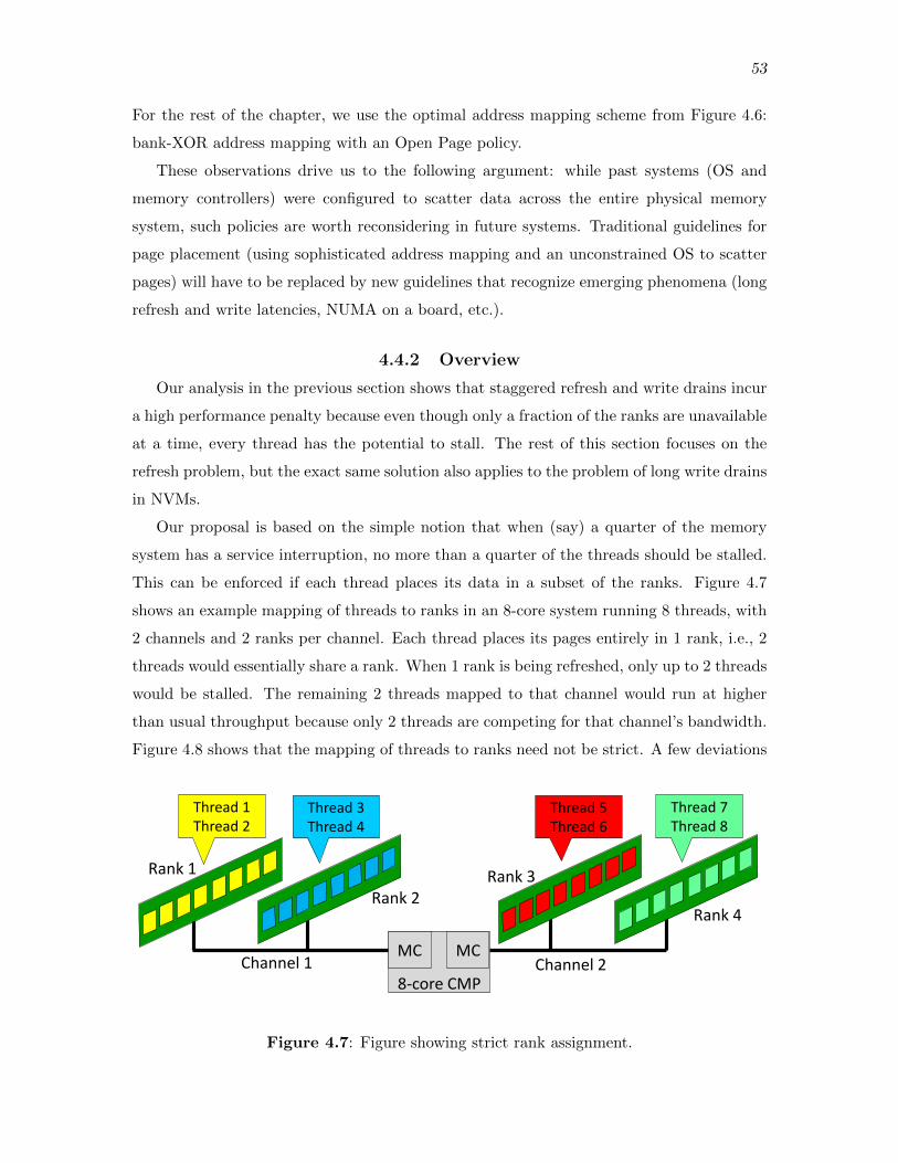
53
For the rest of the chapter, we use the optimal address mapping scheme from Figure 4.6:
bank-XOR address mapping with an Open Page policy.
These observations drive us to the following argument: while past systems (OS and
memory controllers) were configured to scatter data across the entire physical memory
system, such policies are worth reconsidering in future systems. Traditional guidelines for
page placement (using sophisticated address mapping and an unconstrained OS to scatter
pages) will have to be replaced by new guidelines that recognize emerging phenomena (long
refresh and write latencies, NUMA on a board, etc.).
4.4.2 Overview
Our analysis in the previous section shows that staggered refresh and write drains incur
a high performance penalty because even though only a fraction of the ranks are unavailable
at a time, every thread has the potential to stall. The rest of this section focuses on the
refresh problem, but the exact same solution also applies to the problem of long write drains
in NVMs.
Our proposal is based on the simple notion that when (say) a quarter of the memory
system has a service interruption, no more than a quarter of the threads should be stalled.
This can be enforced if each thread places its data in a subset of the ranks. Figure 4.7
shows an example mapping of threads to ranks in an 8-core system running 8 threads, with
2 channels and 2 ranks per channel. Each thread places its pages entirely in 1 rank, i.e., 2
threads would essentially share a rank. When 1 rank is being refreshed, only up to 2 threads
would be stalled. The remaining 2 threads mapped to that channel would run at higher
than usual throughput because only 2 threads are competing for that channel’s bandwidth.
Figure 4.8 shows that the mapping of threads to ranks need not be strict. A few deviations
8-core CMP
MC MCChannel 1 Channel 2
Rank 1
Rank 2Rank 3
Rank 4
Thread 1Thread 2
Thread 3Thread 4
Thread 5Thread 6
Thread 7Thread 8
Figure 4.7: Figure showing strict rank assignment.
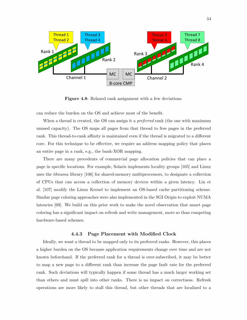
54
8-core CMP
MC MCChannel 1 Channel 2
Rank 1
Rank 2Rank 3
Rank 4
Thread 1Thread 2
Thread 3Thread 4
Thread 5Thread 6
Thread 7Thread 8
Figure 4.8: Relaxed rank assignment with a few deviations.
can reduce the burden on the OS and achieve most of the benefit.
When a thread is created, the OS can assign it a preferred rank (the one with maximum
unused capacity). The OS maps all pages from that thread to free pages in the preferred
rank. This thread-to-rank affinity is maintained even if the thread is migrated to a different
core. For this technique to be effective, we require an address mapping policy that places
an entire page in a rank, e.g., the bank-XOR mapping.
There are many precedents of commercial page allocation policies that can place a
page in specific locations. For example, Solaris implements locality groups [105] and Linux
uses the libnuma library [106] for shared-memory multiprocessors, to designate a collection
of CPUs that can access a collection of memory devices within a given latency. Lin et
al. [107] modify the Linux Kernel to implement an OS-based cache partitioning scheme.
Similar page coloring approaches were also implemented in the SGI Origin to exploit NUMA
latencies [69]. We build on this prior work to make the novel observation that smart page
coloring has a significant impact on refresh and write management, more so than competing
hardware-based schemes.
4.4.3 Page Placement with Modified Clock
Ideally, we want a thread to be mapped only to its preferred ranks. However, this places
a higher burden on the OS because application requirements change over time and are not
known beforehand. If the preferred rank for a thread is over-subscribed, it may be better
to map a new page to a different rank than increase the page fault rate for the preferred
rank. Such deviations will typically happen if some thread has a much larger working set
than others and must spill into other ranks. There is no impact on correctness. Refresh
operations are more likely to stall this thread, but other threads that are localized to a
55
single rank will continue to experience high throughput during most refresh operations.
To reduce the burden on the OS, we consider a modified Clock replacement policy [108]
that is simple and approximates the ideal assignment of threads to ranks. Muralidhara et
al. [109] also use a similar page mapping algorithm to map pages to channels. The baseline
Clock policy maintains a circular list of all pages, a bit for each page to indicate if it has
been touched recently (reference bit), and a global pointer to the next eviction candidate.
When a new page is requested, the pointer moves forward until an unreferenced page is
found. All pages that are encountered in this search are marked unreferenced.
In our page allocator, when a thread is spawned, the OS looks for a rank that has the least
utilization and that rank is assigned as the preferred rank for the new thread. Utilization
is defined as the average queuing delay for that rank, where queuing delay includes wait
time for the channel and wait time for page fault handling. Instead of 1 global pointer,
the page allocator maintains a pointer for each rank. When a thread assigned to rank R1
requests a free page, the pointer for R1 is advanced. The pointer only looks for unreferenced
pages belonging to R1. Unlike the baseline policy, encountered pages during this walk are
not unreferenced. Ultimately, an unreferenced page may be found – this page is used by
the thread and marked as referenced (so it is not used by trailing pointers). If the pointer
reaches the last page in the list without finding an unreferenced page, it gives up and
performs another walk, looking for a page from a second preferred rank. If that walk fails
as well, we resort to the baseline Clock algorithm to find any unreferenced page, starting
from the rank pointer that is trailing all other rank pointers. When all rank pointers reach
the end of the list, the pointers roll to the start. Before rolling over, the reference bits for
all pages are reset (with the exception of pages currently resident in the processor’s TLBs).
This reset process is common to the baseline and proposed allocators.
Consider an example with an aggressor thread T1 with a large and active working set
co-scheduled with a submissive thread T2 with a small working set. T1 is assigned to rank
R1 and T2 is assigned to rank R2. When T1 requests a page, it is preferentially allocated
pages from R1. Its pointer quickly reaches the end of the list because many pages in R1 are
marked as referenced. From that point on, subsequent pages are allocated from R2 until
R2’s pointer also reaches the end of the list. This algorithm does not lead to any additional
page faults, but steers T1 to R1 as much as possible. Once the pointers roll over, at first,
T1 evicts its own pages to make room for its pages. The baseline, on the other hand, would
evict some of T2’s pages to make room for T1’s pages. We observed that the new policy
leads to fewer page faults. This is because the aggressor thread has longer reuse distances,
56
while the submissive thread has shorter reuse distances. Therefore, after the pointers have
rolled over, it is better to evict the aggressor thread’s pages than the submissive thread’s
pages.
4.4.4 Multithreaded Applications
A potential problem with the rank assignment approach is that while multiprogrammed
workloads can be controlled to only access a single rank, multithreaded workloads may not
be as easy to control. If a thread accesses a page that was created by another thread, the
thread’s accesses may no longer be localized to a single rank. The probability of this depends
strongly on how much page sharing is exhibited by the application. In our benchmark suite,
canneal had the least locality; up to 62.5% of accesses were steered to a rank different from
the thread’s assigned rank. As stated before, when such deviations happen, it only limits
the performance improvement, but does not cause correctness problems. Regardless of what
we observe on our benchmark suite, it is clear that the rank assignment approach will not
be effective for some workload classes. For example, a web server is likely to have very low
thread-to-rank affinity; when a request shows up, it is serviced by the first available core
and the data for that request may reside in any of the ranks. For such a workload, a service
interruption in a rank has the potential to stall all threads.
4.5 Other Schemes Tried: Eager Refresh
The JEDEC DDR4 [3] standard offers the memory controller the flexibility to issue
refreshes at any time within a window. As long as 8 refreshes have been issued within a
window of 8 refresh intervals (8×tREFI), the data in the DRAM are preserved.
Instead of issuing refreshes at hard tREFI boundaries, eager refresh tries to issue
refreshes to a rank as soon as the read queue of the rank is empty and the command
bus is free. Unlike Deferred until Empty (DUE) refresh [76], eager refresh does not wait
until the tREFI deadline has passed, but issues the eefresh eagerly if the rank has no
pending requests. This reduces the balance of eefreshes that are left at the end of the
8×tREFI deadline. Any eefreshes that are left over are forced at the end the 8×tREFI.
Our experiment showed that very often there were eefreshes that were not issued eagerly
and needed to be enforced. Our experiments also showed that the long latencies caused
by the successive eefreshes that were forced were extremely detrimental to performance.
Eager eefresh was tried with fine grained eefresh also. Eager eefresh yielded less than 1%
performance improvement.
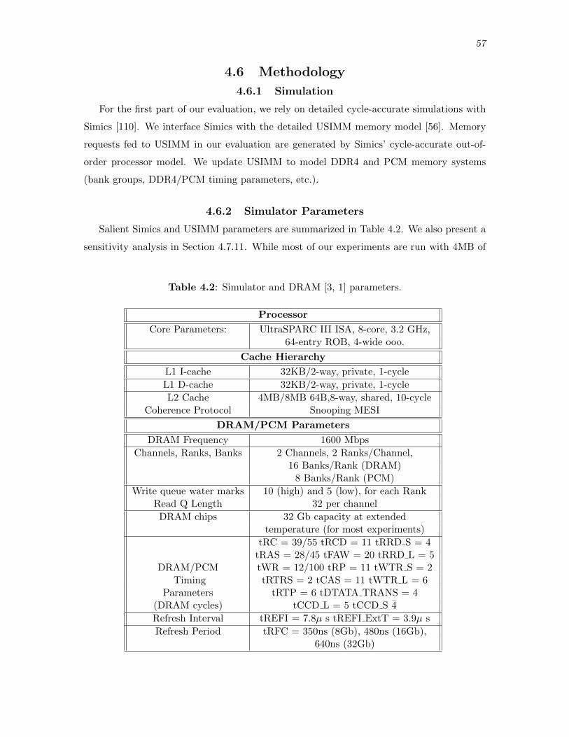
57
4.6 Methodology
4.6.1 Simulation
For the first part of our evaluation, we rely on detailed cycle-accurate simulations with
Simics [110]. We interface Simics with the detailed USIMM memory model [56]. Memory
requests fed to USIMM in our evaluation are generated by Simics’ cycle-accurate out-of-
order processor model. We update USIMM to model DDR4 and PCM memory systems
(bank groups, DDR4/PCM timing parameters, etc.).
4.6.2 Simulator Parameters
Salient Simics and USIMM parameters are summarized in Table 4.2. We also present a
sensitivity analysis in Section 4.7.11. While most of our experiments are run with 4MB of
Table 4.2: Simulator and DRAM [3, 1] parameters.
Processor
Core Parameters: UltraSPARC III ISA, 8-core, 3.2 GHz,64-entry ROB, 4-wide ooo.
Cache Hierarchy
L1 I-cache 32KB/2-way, private, 1-cycle
L1 D-cache 32KB/2-way, private, 1-cycle
L2 Cache 4MB/8MB 64B,8-way, shared, 10-cycleCoherence Protocol Snooping MESI
DRAM/PCM Parameters
DRAM Frequency 1600 Mbps
Channels, Ranks, Banks 2 Channels, 2 Ranks/Channel,16 Banks/Rank (DRAM)
8 Banks/Rank (PCM)
Write queue water marks 10 (high) and 5 (low), for each RankRead Q Length 32 per channel
DRAM chips 32 Gb capacity at extendedtemperature (for most experiments)
tRC = 39/55 tRCD = 11 tRRD S = 4tRAS = 28/45 tFAW = 20 tRRD L = 5
DRAM/PCM tWR = 12/100 tRP = 11 tWTR S = 2Timing tRTRS = 2 tCAS = 11 tWTR L = 6
Parameters tRTP = 6 tDTATA TRANS = 4(DRAM cycles) tCCD L = 5 tCCD S 4
Refresh Interval tREFI = 7.8µ s tREFI ExtT = 3.9µ s
Refresh Period tRFC = 350ns (8Gb), 480ns (16Gb),640ns (32Gb)
58
L2 cache, as part of our sensitivity analysis, we also provide performance results with 8MB
of L2 cache.
We adopt the bank-XOR address mapping policy. Our memory scheduler prioritizes
row buffer hits, and uses an Open Page policy. Reads are prioritized over writes until the
write queue reaches a high water mark. The choice of memory scheduler is orthogonal to
the refresh mechanism.
4.6.3 Peak Power Model
Our proposals do not impact the total activity within the memory system. By improving
throughput, they have the potential to yield lower memory and system energy for a given
task. The choice of staggered or simultaneous refresh does influence the peak memory
power, already described in Section 4.3. We rely on the Micron power calculator for x4
4 Gb DRAM chips for those estimates [98].
4.6.4 Workloads
We use multiprogrammed workloads constructed out of SPEC2k6 benchmarks and
multithreaded workloads from PARSEC [111], NAS Parallel Benchmarks (NPB), and Cloud-
Suite [112]. For SPEC2k6, we run 8 instances of each benchmark (rate mode). CloudSuite,
PARSEC, and NPB are run with 8 threads. The SPEC workloads are fast-forwarded
for 50 billion instructions before starting simulations and the NPB/CloudSuite/PARSEC
programs are simulated at the start of their region of interest. The measurements in the
early part of our cycle-accurate simulations are discarded to account for various warm-up
effects. Measurements are reported for 2 million DRAM accesses, which corresponds to
82M-1.5B total simulated instructions for each workload. Longer simulations do not impact
our result trends much – note that our proposals do not introduce new predictors or caches
that would require longer simulations for reliable evaluation. By using DRAM access count
to terminate an experiment, we ensure that each experiment measures roughly an equal
amount of work. In the multiprogrammed workloads, each program makes roughly equal
progress in every experiment (we are running in rate mode and our policies do not prioritize
any particular thread). We have confirmed this by examining several parameters that are
roughly invariants across each experiment for a given workload (e.g., number of reads/writes,
branches, etc.). Any slippage in multithreaded workloads is compensated by wait times at
barriers. Spinning at a barrier can increase instruction count (hence, IPC is a bad metric
for multithreaded workloads), but does not increase memory accesses (the metric we use to
define roughly equal amounts of work in each experiment).
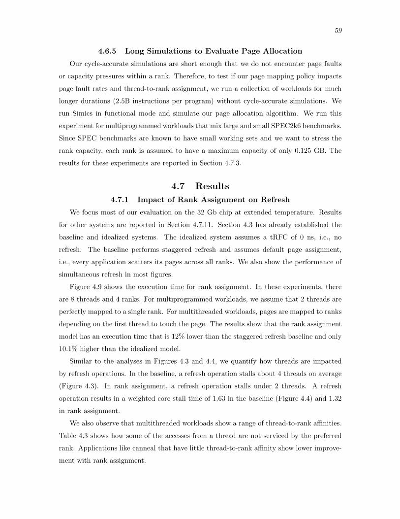
59
4.6.5 Long Simulations to Evaluate Page Allocation
Our cycle-accurate simulations are short enough that we do not encounter page faults
or capacity pressures within a rank. Therefore, to test if our page mapping policy impacts
page fault rates and thread-to-rank assignment, we run a collection of workloads for much
longer durations (2.5B instructions per program) without cycle-accurate simulations. We
run Simics in functional mode and simulate our page allocation algorithm. We run this
experiment for multiprogrammed workloads that mix large and small SPEC2k6 benchmarks.
Since SPEC benchmarks are known to have small working sets and we want to stress the
rank capacity, each rank is assumed to have a maximum capacity of only 0.125 GB. The
results for these experiments are reported in Section 4.7.3.
4.7 Results
4.7.1 Impact of Rank Assignment on Refresh
We focus most of our evaluation on the 32 Gb chip at extended temperature. Results
for other systems are reported in Section 4.7.11. Section 4.3 has already established the
baseline and idealized systems. The idealized system assumes a tRFC of 0 ns, i.e., no
refresh. The baseline performs staggered refresh and assumes default page assignment,
i.e., every application scatters its pages across all ranks. We also show the performance of
simultaneous refresh in most figures.
Figure 4.9 shows the execution time for rank assignment. In these experiments, there
are 8 threads and 4 ranks. For multiprogrammed workloads, we assume that 2 threads are
perfectly mapped to a single rank. For multithreaded workloads, pages are mapped to ranks
depending on the first thread to touch the page. The results show that the rank assignment
model has an execution time that is 12% lower than the staggered refresh baseline and only
10.1% higher than the idealized model.
Similar to the analyses in Figures 4.3 and 4.4, we quantify how threads are impacted
by refresh operations. In the baseline, a refresh operation stalls about 4 threads on average
(Figure 4.3). In rank assignment, a refresh operation stalls under 2 threads. A refresh
operation results in a weighted core stall time of 1.63 in the baseline (Figure 4.4) and 1.32
in rank assignment.
We also observe that multithreaded workloads show a range of thread-to-rank affinities.
Table 4.3 shows how some of the accesses from a thread are not serviced by the preferred
rank. Applications like canneal that have little thread-to-rank affinity show lower improve-
ment with rank assignment.
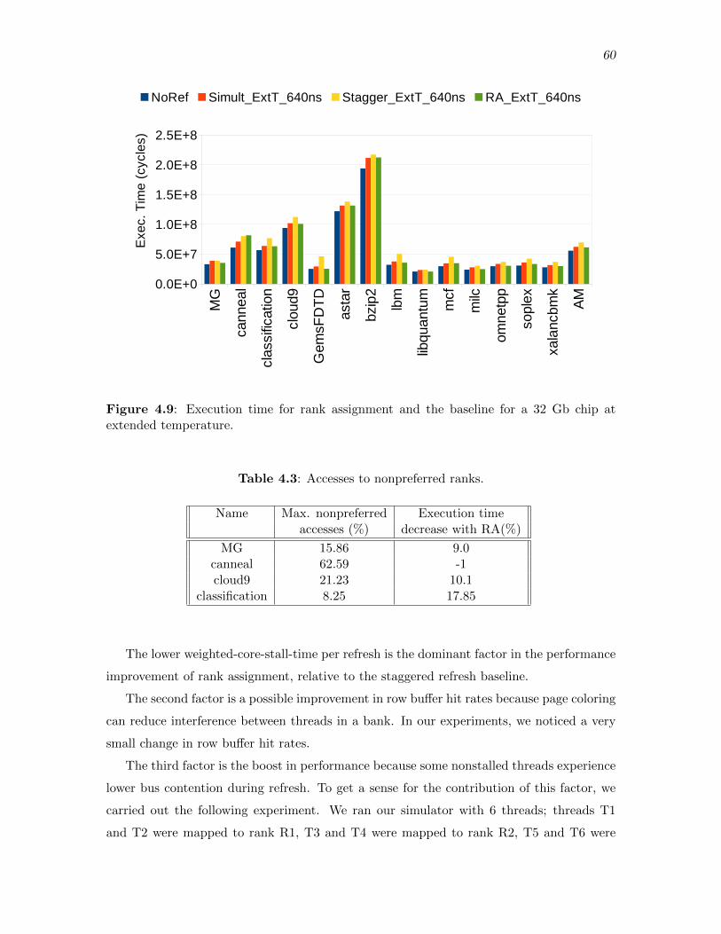
60
MG
cann
eal
clas
sific
atio
n
clou
d9
Gem
sFD
TD
asta
r
bzip
2
lbm
libqu
antu
m
mcf
milc
omne
tpp
sopl
ex
xala
ncbm
k
AM
0.0E+0
5.0E+7
1.0E+8
1.5E+8
2.0E+8
2.5E+8
NoRef Simult_ExtT_640ns Stagger_ExtT_640ns RA_ExtT_640ns
Exe
c. T
ime
(cy
cle
s)
Figure 4.9: Execution time for rank assignment and the baseline for a 32 Gb chip atextended temperature.
Table 4.3: Accesses to nonpreferred ranks.
Name Max. nonpreferred Execution timeaccesses (%) decrease with RA(%)
MG 15.86 9.0canneal 62.59 -1cloud9 21.23 10.1
classification 8.25 17.85
The lower weighted-core-stall-time per refresh is the dominant factor in the performance
improvement of rank assignment, relative to the staggered refresh baseline.
The second factor is a possible improvement in row buffer hit rates because page coloring
can reduce interference between threads in a bank. In our experiments, we noticed a very
small change in row buffer hit rates.
The third factor is the boost in performance because some nonstalled threads experience
lower bus contention during refresh. To get a sense for the contribution of this factor, we
carried out the following experiment. We ran our simulator with 6 threads; threads T1
and T2 were mapped to rank R1, T3 and T4 were mapped to rank R2, T5 and T6 were
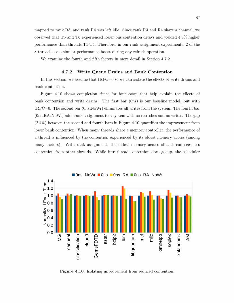
61
mapped to rank R3, and rank R4 was left idle. Since rank R3 and R4 share a channel, we
observed that T5 and T6 experienced lower bus contention delays and yielded 4.8% higher
performance than threads T1-T4. Therefore, in our rank assignment experiments, 2 of the
8 threads see a similar performance boost during any refresh operation.
We examine the fourth and fifth factors in more detail in Section 4.7.2.
4.7.2 Write Queue Drains and Bank Contention
In this section, we assume that tRFC=0 so we can isolate the effects of write drains and
bank contention.
Figure 4.10 shows completion times for four cases that help explain the effects of
bank contention and write drains. The first bar (0ns) is our baseline model, but with
tRFC=0. The second bar (0ns NoWr) eliminates all writes from the system. The fourth bar
(0ns RA NoWr) adds rank assignment to a system with no refreshes and no writes. The gap
(2.4%) between the second and fourth bars in Figure 4.10 quantifies the improvement from
lower bank contention. When many threads share a memory controller, the performance of
a thread is influenced by the contention experienced by its oldest memory access (among
many factors). With rank assignment, the oldest memory access of a thread sees less
contention from other threads. While intrathread contention does go up, the scheduler
MG
cann
eal
clas
sific
atio
n
clou
d9
Gem
sFD
TD
asta
r
bzip
2
lbm
libqu
antu
m
mcf
milc
omne
tpp
sopl
ex
xala
ncbm
k
AM
0.0
0.2
0.4
0.6
0.8
1.0
1.2
1.4
0ns_NoWr 0ns 0ns_RA 0ns_RA_NoWr
No
rma
lize
d E
xec.
Tim
e
Figure 4.10: Isolating improvement from reduced contention.
62
already prioritizes the older memory accesses.
The third bar (0ns RA) in Figure 4.10 shows a system with no refresh and page coloring.
The gap between the first and third bars (5.9%) in Figure 4.10 quantifies the combined
benefit from lower bank contention and fewer stalls during write drains. We estimate that
the fewer stalls during write drains by itself can improve performance of DRAM systems
by 3.5%.
In summary, even though tRFC/tREFI is 16% for 32GB chips at extended temperatures,
the observed penalty is only 10%. This is because different factors play roles in augmenting
the benefits from page coloring: some overlap of computation with refresh, higher row
buffer hit rates, higher throughput for nonstalled threads, lower bank contention, and more
efficient write queue drains. The last four factors are not present in the simultaneous refresh
baseline. Hence, rank assignment is able to out-perform simultaneous refresh by 4.1%, while
having much lower memory peak power. The improvement relative to the staggered refresh
baseline is much higher (12%).
4.7.3 Page Allocation Disruptions
Due to low simulation speeds, our cycle-accurate simulations last under 226 million
processor cycles per core. In such experiments, we are able to perfectly map threads to
ranks. Such simulations are not long enough to exhibit possible disruptions from the new
page allocation algorithm. In particular, when different threads have varying working set
sizes, it is possible that some threads may spread their pages across multiple ranks, or by
forcing a large thread to steer most of its pages to 1 rank, it may incur a high page fault
rate.
To test the algorithm described in Section 4.4.3 on a heterogeneous workload, we run the
programs in functional mode with Simics and track all page accesses. We assume that each
rank has a capacity of 0.125 GB. Our workloads consist of four threads of varying working
set sizes. We simulate these for 10B total instructions (2.5B instructions/core x 4 cores).
We consider the following workloads composed of large and small working set benchmarks:
lbm-libquantum-astar-milc, and astar-milc-soplex-xalancbmk.
Our results show that 30% of all accesses made by a thread are not to its assigned rank
or the second-preferred rank. Figure 4.11 shows that the effectiveness of rank assignment
decreases as pages from a thread are spread over more ranks. The Y-axis represents the
execution time decrease and the X-axis represents percentage of pages that are mapped to
a random rank (that is not the assigned rank). Even with a 50% page mapping error, rank
assignment reduces execution time by 9.4%
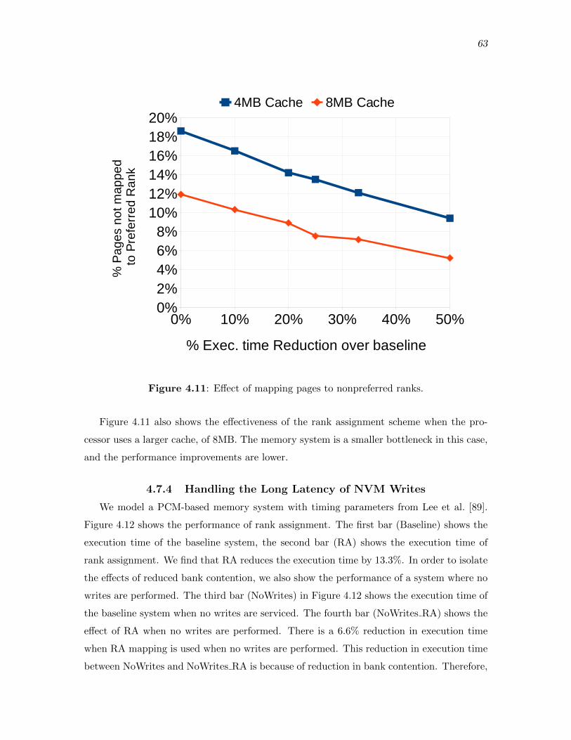
63
0% 10% 20% 30% 40% 50%0%2%4%6%8%
10%12%14%16%18%20%
4MB Cache 8MB Cache
% Exec. time Reduction over baseline
% P
ag
es
no
t m
ap
pe
d t
o P
refe
rre
d R
an
k
Figure 4.11: Effect of mapping pages to nonpreferred ranks.
Figure 4.11 also shows the effectiveness of the rank assignment scheme when the pro-
cessor uses a larger cache, of 8MB. The memory system is a smaller bottleneck in this case,
and the performance improvements are lower.
4.7.4 Handling the Long Latency of NVM Writes
We model a PCM-based memory system with timing parameters from Lee et al. [89].
Figure 4.12 shows the performance of rank assignment. The first bar (Baseline) shows the
execution time of the baseline system, the second bar (RA) shows the execution time of
rank assignment. We find that RA reduces the execution time by 13.3%. In order to isolate
the effects of reduced bank contention, we also show the performance of a system where no
writes are performed. The third bar (NoWrites) in Figure 4.12 shows the execution time of
the baseline system when no writes are serviced. The fourth bar (NoWrites RA) shows the
effect of RA when no writes are performed. There is a 6.6% reduction in execution time
when RA mapping is used when no writes are performed. This reduction in execution time
between NoWrites and NoWrites RA is because of reduction in bank contention. Therefore,
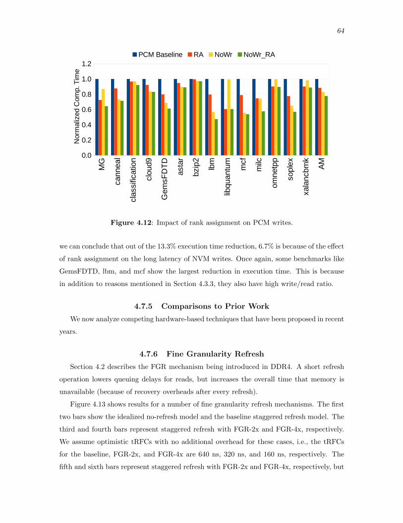
64
MG
cann
eal
clas
sific
atio
n
clou
d9
Gem
sFD
TD
asta
r
bzip
2
lbm
libqu
antu
m
mcf
milc
omne
tpp
sopl
ex
xala
ncbm
k
AM
0.0
0.2
0.4
0.6
0.8
1.0
1.2PCM Baseline RA NoWr NoWr_RA
Nor
mal
ized
Com
p. T
ime
Figure 4.12: Impact of rank assignment on PCM writes.
we can conclude that out of the 13.3% execution time reduction, 6.7% is because of the effect
of rank assignment on the long latency of NVM writes. Once again, some benchmarks like
GemsFDTD, lbm, and mcf show the largest reduction in execution time. This is because
in addition to reasons mentioned in Section 4.3.3, they also have high write/read ratio.
4.7.5 Comparisons to Prior Work
We now analyze competing hardware-based techniques that have been proposed in recent
years.
4.7.6 Fine Granularity Refresh
Section 4.2 describes the FGR mechanism being introduced in DDR4. A short refresh
operation lowers queuing delays for reads, but increases the overall time that memory is
unavailable (because of recovery overheads after every refresh).
Figure 4.13 shows results for a number of fine granularity refresh mechanisms. The first
two bars show the idealized no-refresh model and the baseline staggered refresh model. The
third and fourth bars represent staggered refresh with FGR-2x and FGR-4x, respectively.
We assume optimistic tRFCs with no additional overhead for these cases, i.e., the tRFCs
for the baseline, FGR-2x, and FGR-4x are 640 ns, 320 ns, and 160 ns, respectively. The
fifth and sixth bars represent staggered refresh with FGR-2x and FGR-4x, respectively, but
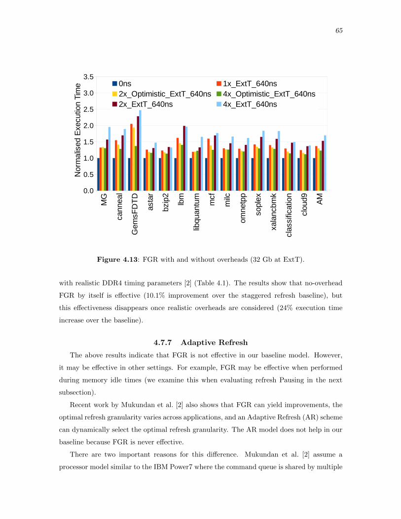
65
MG
cann
eal
Gem
sFD
TD
asta
r
bzip
2
lbm
libqu
antu
m
mcf
milc
omne
tpp
sopl
ex
xala
ncbm
k
clas
sific
atio
n
clou
d9 AM
0.0
0.5
1.0
1.5
2.0
2.5
3.0
3.50ns 1x_ExtT_640ns2x_Optimistic_ExtT_640ns 4x_Optimistic_ExtT_640ns2x_ExtT_640ns 4x_ExtT_640ns
Nor
mal
ised
Exe
cutio
n Ti
me
Figure 4.13: FGR with and without overheads (32 Gb at ExtT).
with realistic DDR4 timing parameters [2] (Table 4.1). The results show that no-overhead
FGR by itself is effective (10.1% improvement over the staggered refresh baseline), but
this effectiveness disappears once realistic overheads are considered (24% execution time
increase over the baseline).
4.7.7 Adaptive Refresh
The above results indicate that FGR is not effective in our baseline model. However,
it may be effective in other settings. For example, FGR may be effective when performed
during memory idle times (we examine this when evaluating refresh Pausing in the next
subsection).
Recent work by Mukundan et al. [2] also shows that FGR can yield improvements, the
optimal refresh granularity varies across applications, and an Adaptive Refresh (AR) scheme
can dynamically select the optimal refresh granularity. The AR model does not help in our
baseline because FGR is never effective.
There are two important reasons for this difference. Mukundan et al. [2] assume a
processor model similar to the IBM Power7 where the command queue is shared by multiple
66
ranks. This leads to command queue seizure in their baseline, where requests to a rank being
refreshed take up most of the command queue entries and throttle memory throughput. In
our simulation model, we assume per-rank command queues, so the entries waiting for a
rank being refreshed do not impact throughput in other ranks. Even when we assume a
single command queue for all ranks, we observe that command queue seizure is rare if we
assume a 32-entry read queue. For an 8-core system to fill up a 32-entry read queue, each
64-entry ROB must average more than 4 misses, i.e., a per-thread MPKI higher than 62.5,
which is relatively uncommon.
In our simulation model, we see that Preemptive Command Drain (PCD) [2] reduces
execution time by 0.9%.
4.7.8 Refresh Pausing
Refresh Pausing (RP) [77] begins a refresh operation as soon as a rank is idle, but
pauses it when the memory controller receives a request from the CPU. Refresh Pausing
partitions the refresh operation into smaller fragments and squeezes them into idle periods.
We model an optimistic version of RP that resembles the model in the original paper [77]
and a realistic version of RP that is based on the recently released DDR4 timing parameters.
The optimistic version of RP (formulated before DDR4 timing was revealed) assumes that
a 640 ns refresh operation can be paused up to 8 times, where each fragment takes 80 ns.
We assume that DDR4 FGR timing is a reasonable commercial estimate of the timing for
smaller refresh operations. Similar to DDR4’s FGR, we assume that the realistic version of
RP can be paused only at FGR intervals. Figure 4.14 shows a significant (14%) execution
time reduction with optimistic RP, but an overall increase in execution time (7.2%) when
FGR overheads are added.
4.7.9 Elastic Refresh
Elastic Refresh (ER) [76] tries to perform refresh when the memory is idle. The DDR3
standard requires that 8 refresh operations be performed within an 8×tREFI time window,
but allows the memory controller some flexibility in when to issue those refresh operations.
If ER detects that the rank has been idle for a specified time, it issues a refresh command.
Any leftover refreshes have to be issued at the end of the 8×tREFI time window. We model
the static ER scheme described in [76]. Figure 4.15 shows the potential benefit with this
scheme (4.2% over the baseline).
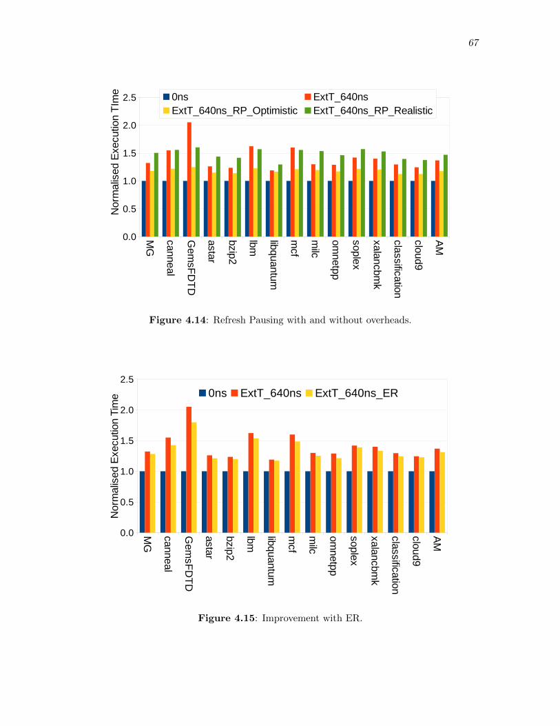
67
MG
canne al
Gem
s FD
TD
astar
bzip2
lbm
libquan tum
mcf
milc
omnet pp
soplex
xalanc bmk
classif ication
cloud9
AM
0.0
0.5
1.0
1.5
2.0
2.5 0ns ExtT_640nsExtT_640ns_RP_Optimistic ExtT_640ns_RP_Realistic
Nor
mal
ised
Exe
cutio
n T
Ime
Figure 4.14: Refresh Pausing with and without overheads.
MG
canne al
Gem
s FD
TD
astar
bzip2
lbm
libquan tum
mcf
milc
omnet pp
soplex
xalanc bmk
classif ication
cloud9
AM
0.0
0.5
1.0
1.5
2.0
2.5
0ns ExtT_640ns ExtT_640ns_ER
Nor
mal
ised
Exe
cutio
n Ti
me
Figure 4.15: Improvement with ER.
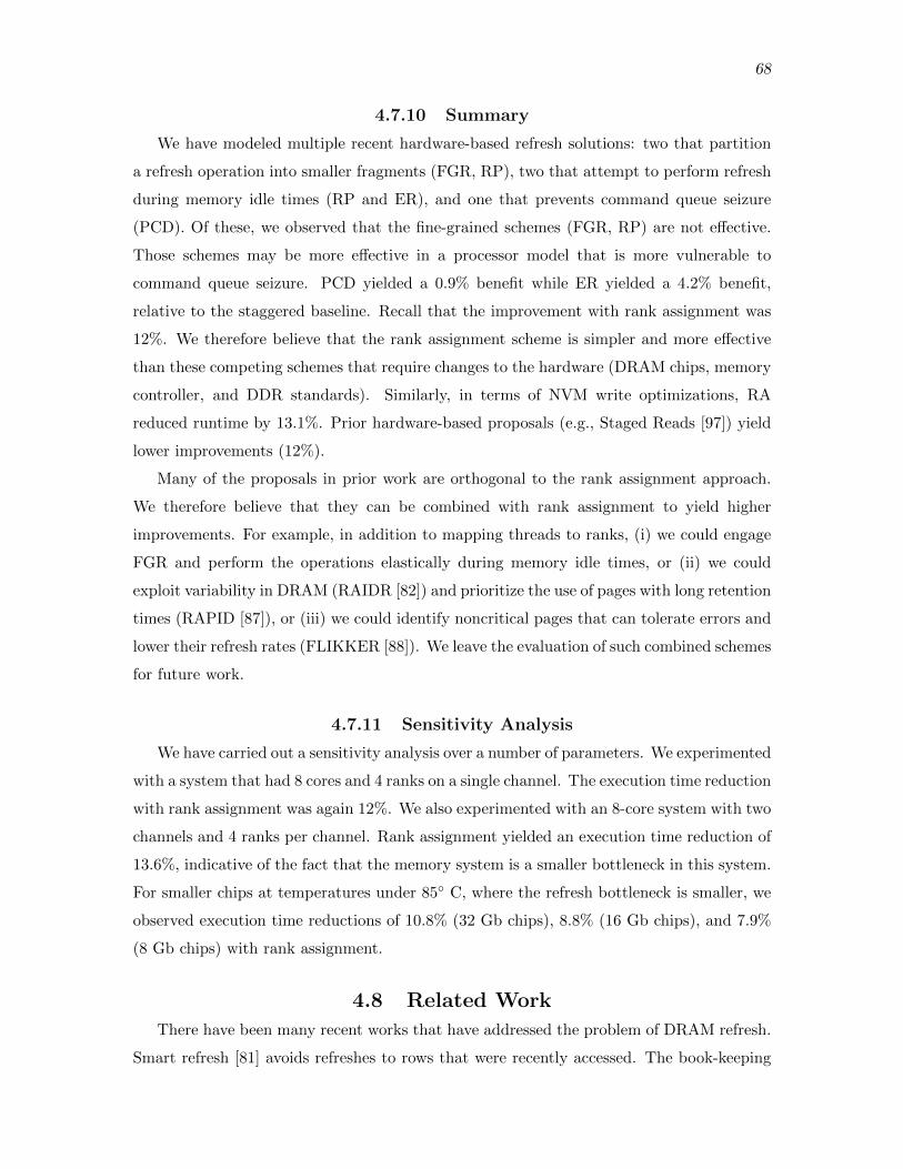
68
4.7.10 Summary
We have modeled multiple recent hardware-based refresh solutions: two that partition
a refresh operation into smaller fragments (FGR, RP), two that attempt to perform refresh
during memory idle times (RP and ER), and one that prevents command queue seizure
(PCD). Of these, we observed that the fine-grained schemes (FGR, RP) are not effective.
Those schemes may be more effective in a processor model that is more vulnerable to
command queue seizure. PCD yielded a 0.9% benefit while ER yielded a 4.2% benefit,
relative to the staggered baseline. Recall that the improvement with rank assignment was
12%. We therefore believe that the rank assignment scheme is simpler and more effective
than these competing schemes that require changes to the hardware (DRAM chips, memory
controller, and DDR standards). Similarly, in terms of NVM write optimizations, RA
reduced runtime by 13.1%. Prior hardware-based proposals (e.g., Staged Reads [97]) yield
lower improvements (12%).
Many of the proposals in prior work are orthogonal to the rank assignment approach.
We therefore believe that they can be combined with rank assignment to yield higher
improvements. For example, in addition to mapping threads to ranks, (i) we could engage
FGR and perform the operations elastically during memory idle times, or (ii) we could
exploit variability in DRAM (RAIDR [82]) and prioritize the use of pages with long retention
times (RAPID [87]), or (iii) we could identify noncritical pages that can tolerate errors and
lower their refresh rates (FLIKKER [88]). We leave the evaluation of such combined schemes
for future work.
4.7.11 Sensitivity Analysis
We have carried out a sensitivity analysis over a number of parameters. We experimented
with a system that had 8 cores and 4 ranks on a single channel. The execution time reduction
with rank assignment was again 12%. We also experimented with an 8-core system with two
channels and 4 ranks per channel. Rank assignment yielded an execution time reduction of
13.6%, indicative of the fact that the memory system is a smaller bottleneck in this system.
For smaller chips at temperatures under 85 C, where the refresh bottleneck is smaller, we
observed execution time reductions of 10.8% (32 Gb chips), 8.8% (16 Gb chips), and 7.9%
(8 Gb chips) with rank assignment.
4.8 Related Work
There have been many recent works that have addressed the problem of DRAM refresh.
Smart refresh [81] avoids refreshes to rows that were recently accessed. The book-keeping
69
overheads for this approach increase with DRAM capacity. Elastic Refresh [76] tries to
predict lulls in activity and tries to schedule refreshes during the lull. Flikker [88] uses the
OS to identify areas of the physical memory that are not storing critical data, and relaxes
the refresh constraints in these areas. RAIDR [82] characterizes the retention characteristics
of rows and uses this to increase the refresh interval of these rows. Retention characteristics
of DRAM are not entirely deterministic. Also, techniques like RAIDR and Smart Refresh
increase the utilization of the Command/Address bus. Owing to increased number of banks
in DDR4, we have seen that the utilization of command and data bus is quite high. Nair et
al. [77] propose Refresh Pausing, where a refresh operation can be interrupted after a few
rows have been refreshed, in case a read is waiting.
Many techniques have been proposed to mitigate the long latency of PCM writes. Lee
et al. [89] use narrow rows to mitigate the high latency of PCM. Yue et al. [94] and Qureshi
et al. [91] make use of the asymmetric nature of PCM writes to speed up the write process.
Jiang et al. [92] limit the number of write iterations performed, and use ECC to correct
any bits that are incorrectly written. Qureshi et al. [90] pause the iterative write process in
PCM when a read request arrives, thereby avoiding stalls because of the long write latency.
All the techniques mentioned above are orthogonal to our proposal. Rank assignment
attempts to keep the memory channel busy even when certain parts of the channel are
refreshing. Unlike many of the proposals listed above, rank assignment does not incur
power or storage over heads.
Liu et al. [95] modify the Linux 2.6.32.15 kernel to implement thread to bank mapping.
They show that most workloads can achieve 90% of their max. performance with only 16
DRAM banks. Xie et al. [113] dynamically assign banks to threads based on the memory
characteristics of the thread.
Muralidhara et al. [109] map pages to DRAM channels based on the MPKI and DRAM
row buffer hit rate of the application. This helps reduce bank contention and also prioritize
performance critical DRAM accesses. The implementation of our rank assignment mapping
is partly inspired by the implementation presented in [109].
4.9 Conclusions
This chapter considers a simple technique to hide service interruptions in future DRAMs
and NVMs. Service interruptions such as refresh and write drains happen at the granularity
of ranks. We show that fine-grained refresh approaches, as supported by DDR4, are not
effective in hiding refresh penalties. Our experiments with elastic forms of refresh also
yielded small improvements. By mapping pages from a thread to few ranks, we show that
70
it is possible to stall only a fraction of threads when a rank is interrupted. The rank
assignment mechanism is effective in removing a large fraction of refresh and write drain
overheads, while requiring no changes to the hardware. The only modifications are to the
OS, which only has to perform a best-effort mapping of threads to ranks.
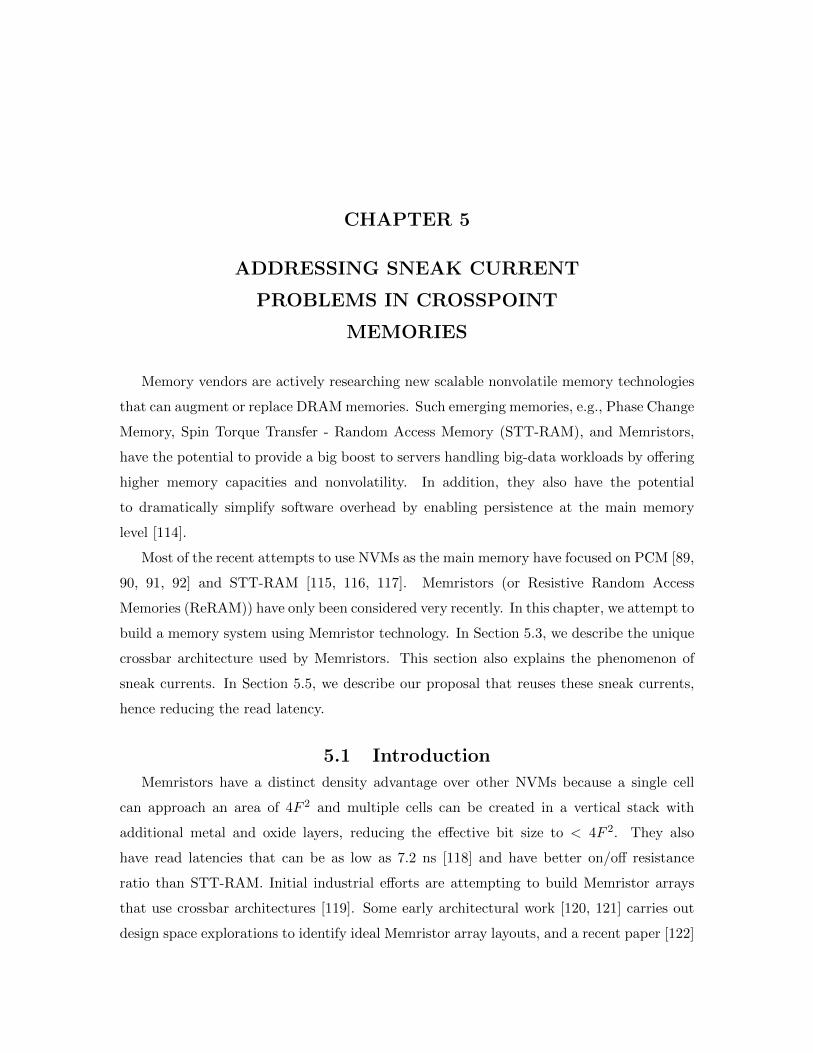
CHAPTER 5
ADDRESSING SNEAK CURRENT
PROBLEMS IN CROSSPOINT
MEMORIES
Memory vendors are actively researching new scalable nonvolatile memory technologies
that can augment or replace DRAM memories. Such emerging memories, e.g., Phase Change
Memory, Spin Torque Transfer - Random Access Memory (STT-RAM), and Memristors,
have the potential to provide a big boost to servers handling big-data workloads by offering
higher memory capacities and nonvolatility. In addition, they also have the potential
to dramatically simplify software overhead by enabling persistence at the main memory
level [114].
Most of the recent attempts to use NVMs as the main memory have focused on PCM [89,
90, 91, 92] and STT-RAM [115, 116, 117]. Memristors (or Resistive Random Access
Memories (ReRAM)) have only been considered very recently. In this chapter, we attempt to
build a memory system using Memristor technology. In Section 5.3, we describe the unique
crossbar architecture used by Memristors. This section also explains the phenomenon of
sneak currents. In Section 5.5, we describe our proposal that reuses these sneak currents,
hence reducing the read latency.
5.1 Introduction
Memristors have a distinct density advantage over other NVMs because a single cell
can approach an area of 4F 2 and multiple cells can be created in a vertical stack with
additional metal and oxide layers, reducing the effective bit size to < 4F 2. They also
have read latencies that can be as low as 7.2 ns [118] and have better on/off resistance
ratio than STT-RAM. Initial industrial efforts are attempting to build Memristor arrays
that use crossbar architectures [119]. Some early architectural work [120, 121] carries out
design space explorations to identify ideal Memristor array layouts, and a recent paper [122]
72
proposes a few optimizations to reduce read and write latencies for specific Memristor design
styles.
This dissertation adds to this literature by defining Memristor read mechanisms that
significantly improve its performance and energy-efficiency. We start with a tutorial on
Memristor cell and array design that helps identify key challenges and a reasonable baseline
design. We then introduce new “open-column” semantics.
We observe that Memristor array reads require a noisy read of current through the
selected cell as well as a second read of background sneak currents to cancel out the noise.
The latter measurement can be reused when reading other cells in the same column of
the array. Similar to DRAM’s row buffer hit, this introduces the notion of a column hit
in Memristors. Managing the Memristor column requires policies different from those of
DRAM. We also observe that there can be a significant benefit from supporting parallel
reads from many arrays; we therefore consider a number of address mapping policies. Our
results show that performance and energy are best with a policy that places an entire subset
of a page in a single array column.
5.2 Memristor/ReRAM Technology
Memristor, also referred to as ReRAM, is a stateful memory device built by sandwiching
metal oxide material such as TiO2 or HfOx between electrodes [123, 124]. These devices
have at least 2 stable states characterized by either low resistance or high resistance, which
can be used to represent logical 1 and 0.
Resistive memories are broadly classified into either unipolar or bipolar devices based on
their switching modes. In a unipolar device, change in state happens if an external voltage
of specific magnitude and duration is applied across the device, whereas in bipolar devices,
switching of states also depends on the polarity of the external voltage [125, 126, 127, 118].
Even among bipolar devices, there are many metal oxide materials that exhibit resistance
switching. In this work, we focus on a highly scalable, HfOx-based Memristor, which has
an endurance of > 1010 and the cell can be switched at tens of nano seconds [123, 128]. By
carefully architecting the memory array, a HfOx-based Memristor can be used as a main
memory along with or as a replacement to DRAM.
5.3 Array Architecture
Memristor arrays can either be designed as a grid with 1 Transistor 1 Resistor (1T1R)
cells [129] or as a dense crossbar architecture [130]. In a conventional design, each cell has
a dedicated Metal Oxide Semiconductor Field Effect Transistor (MOSFET) transistor (a
73
“1T1R” structure). Similar to DRAM, when a row gets activated, the access transistors
in the selected row provide exclusive access to the cells in that row without disturbing
other cells in the array. This isolation provides better energy efficiency and access time
compared to other array architectures. However, since resistive memories typically operate
at a significantly higher current than DRAM, they require a large sized access transistor
for each cell, making 1T1R cells less compelling for a cost conscious design. As we describe
next, crossbar architectures have the potential to provide significantly higher densities.
5.3.1 Crossbar Architecture
Most emerging resistive memory technologies change their state when a voltage equal
to the switching voltage is applied across the cell. If the potential is less than the switching
voltage, then the cell retains its state without getting disturbed. In contrast, in charge-based
technologies such as DRAM, any nonzero voltage across a cell can disturb its content. This
property of resistive memory along with the nonlinear nature of Memristor, where current
changes nonlinearly with voltage, make it possible to build a unique crossbar architecture.
In a crossbar array (Figure 5.1), a metal layer implements several wordlines and the next
metal layer implements several bitlines. At every overlap point, the bitline and wordline
are fused with metal-oxide material, forming a Memristor cell. If the voltage across a low
resistance state cell exceeds a certain threshold, that cell essentially conducts current from
the wordline to the bitline. Ideally, cells that do not have sufficient voltage across them
should be nonconducting. In practice, a sneak current flows through such cells.
1
Half SelectedCells
Selected Cell
Sneak Current
0V
VMem-
ristor
Selector
Memristor Cell
Figure 5.1: Crossbar array with each cell having a Memristor storage element connectedto a stateless selector device.
74
With such a design, we see that all cells are interconnected to form a dense grid without
any access transistors. By eliminating access transistors, cells in a crossbar achieve the
smallest theoretical size of 4F 2. A cell size of 4F 2 is literally the area under the cross-section
of a minimum sized wordline and bitline. In addition, Memristor cells employ different
fabrication steps from transistors; therefore, the silicon area under the array can be used
for other peripheral circuits such as decoders and drivers, maximizing the area efficiency
of an array. In a highly cost conscious memory market, the crossbar architecture is better
suited for Memristor-based main memory.
In addition to the cell dimension, a Memristor array can also be scaled vertically by
having multiple layers of cells. In a crossbar architecture, it is possible to add a layer on top
of an array by simply adding 2 metal layers with metal-oxide between them. Having 4 such
layers can reduce the effective cell size to 1F 2 [131, 132]. This is different from multilevel
cell technology that stores multiple bits per cell to improve density. This is also different
from 3D die stacking since a single silicon substrate is being layered with many metal and
cell layers. For this work, we consider only a one-layer architecture.
5.3.2 Memristor Reads/Writes
A Memristor crossbar allows reading a single cell at a time. We illustrate this in
Figure 5.2 with an example. If we are trying to read cell (i, j) in an array, a voltage V
is applied to wordline i, and zero voltage is applied to bitline j. All other wordlines and
bitlines are set to a voltage of V/2. As a result, assuming all cells apart from (i, j) are
nonconducting, a voltage of V is applied across cell (i, j), making it a fully selected cell
(the red cell in Figure 5.2). It therefore conducts and a current is received at the bitline
that corresponds to the resistance of the selected cell. The reason that all other cells are
nonconducting is that they have a voltage of V/2 or 0 applied across them. Ideally, that
voltage is low enough to keep the cell in nonconducting state. The cells that have 0 voltage
applied to them (the blue cells in Figure 5.2) are unselected cells and the cells that have
V/2 voltage applied to them (the yellow cells) are half-selected cells.
With this ability to read a single cell at a time, overfetch [38] in Memristor memories can
be eliminated. When reading a cache line, 512 separate 1-bit reads can be performed, either
in parallel or in series, either from 1 array or from 512 different arrays. Similarly, single-bit
writes can also be performed. When writing to cell (i, j), the same setup as Figure 5.2 is
used, except that a voltage VW is applied across the fully-selected cell (and voltage VW /2
is applied to all other wordlines and bitlines). To write the opposite value, VW is applied
to the selected bitline and 0 is applied to the selected wordline.
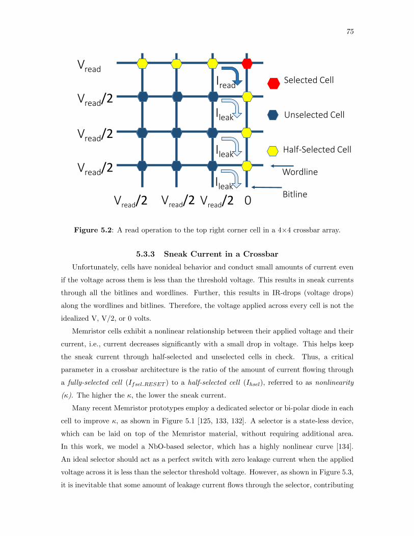
75
Vread
0
Iread
Ileak
Ileak
Ileak
Vread/2
Vread/2
Vread/2
Vread/2 Vread/2Vread/2
Selected Cell
Unselected Cell
Half-Selected Cell
Wordline
Bitline
Figure 5.2: A read operation to the top right corner cell in a 4×4 crossbar array.
5.3.3 Sneak Current in a Crossbar
Unfortunately, cells have nonideal behavior and conduct small amounts of current even
if the voltage across them is less than the threshold voltage. This results in sneak currents
through all the bitlines and wordlines. Further, this results in IR-drops (voltage drops)
along the wordlines and bitlines. Therefore, the voltage applied across every cell is not the
idealized V, V/2, or 0 volts.
Memristor cells exhibit a nonlinear relationship between their applied voltage and their
current, i.e., current decreases significantly with a small drop in voltage. This helps keep
the sneak current through half-selected and unselected cells in check. Thus, a critical
parameter in a crossbar architecture is the ratio of the amount of current flowing through
a fully-selected cell (Ifsel RESET ) to a half-selected cell (Ihsel), referred to as nonlinearity
(κ). The higher the κ, the lower the sneak current.
Many recent Memristor prototypes employ a dedicated selector or bi-polar diode in each
cell to improve κ, as shown in Figure 5.1 [125, 133, 132]. A selector is a state-less device,
which can be laid on top of the Memristor material, without requiring additional area.
In this work, we model a NbO-based selector, which has a highly nonlinear curve [134].
An ideal selector should act as a perfect switch with zero leakage current when the applied
voltage across it is less than the selector threshold voltage. However, as shown in Figure 5.3,
it is inevitable that some amount of leakage current flows through the selector, contributing
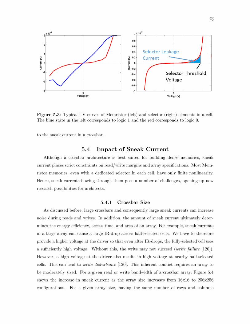
76
Figure 5.3: Typical I-V curves of Memristor (left) and selector (right) elements in a cell.The blue state in the left corresponds to logic 1 and the red corresponds to logic 0.
to the sneak current in a crossbar.
5.4 Impact of Sneak Current
Although a crossbar architecture is best suited for building dense memories, sneak
current places strict constraints on read/write margins and array specifications. Most Mem-
ristor memories, even with a dedicated selector in each cell, have only finite nonlinearity.
Hence, sneak currents flowing through them pose a number of challenges, opening up new
research possibilities for architects.
5.4.1 Crossbar Size
As discussed before, large crossbars and consequently large sneak currents can increase
noise during reads and writes. In addition, the amount of sneak current ultimately deter-
mines the energy efficiency, access time, and area of an array. For example, sneak currents
in a large array can cause a large IR-drop across half-selected cells. We have to therefore
provide a higher voltage at the driver so that even after IR-drops, the fully-selected cell sees
a sufficiently high voltage. Without this, the write may not succeed (write failure [120]).
However, a high voltage at the driver also results in high voltage at nearby half-selected
cells. This can lead to write disturbance [120]. This inherent conflict requires an array to
be moderately sized. For a given read or write bandwidth of a crossbar array, Figure 5.4
shows the increase in sneak current as the array size increases from 16x16 to 256x256
configurations. For a given array size, having the same number of rows and columns
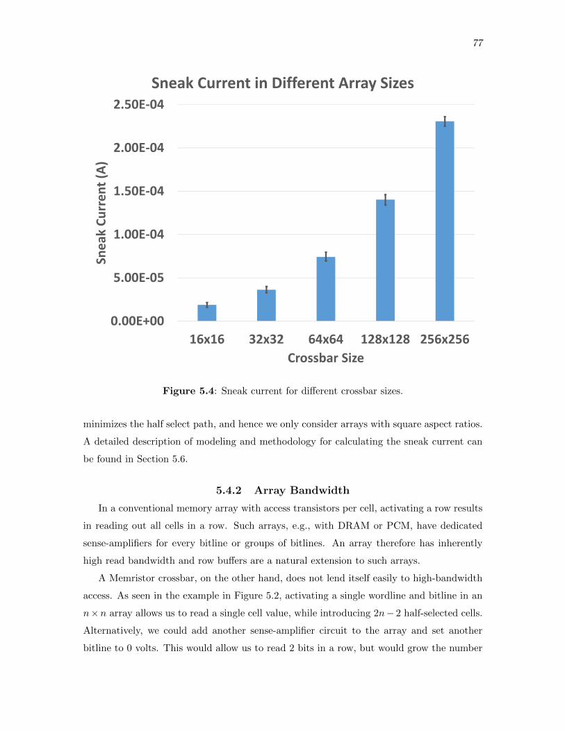
77
0.00E+00
5.00E‐05
1.00E‐04
1.50E‐04
2.00E‐04
2.50E‐04
16x16 32x32 64x64 128x128 256x256
Sneak Cu
rren
t (A)
Crossbar Size
Sneak Current in Different Array Sizes
Figure 5.4: Sneak current for different crossbar sizes.
minimizes the half select path, and hence we only consider arrays with square aspect ratios.
A detailed description of modeling and methodology for calculating the sneak current can
be found in Section 5.6.
5.4.2 Array Bandwidth
In a conventional memory array with access transistors per cell, activating a row results
in reading out all cells in a row. Such arrays, e.g., with DRAM or PCM, have dedicated
sense-amplifiers for every bitline or groups of bitlines. An array therefore has inherently
high read bandwidth and row buffers are a natural extension to such arrays.
A Memristor crossbar, on the other hand, does not lend itself easily to high-bandwidth
access. As seen in the example in Figure 5.2, activating a single wordline and bitline in an
n×n array allows us to read a single cell value, while introducing 2n− 2 half-selected cells.
Alternatively, we could add another sense-amplifier circuit to the array and set another
bitline to 0 volts. This would allow us to read 2 bits in a row, but would grow the number
78
of half-selected cells to 3n − 4. This leads to 2 important drawbacks. First, the energy
for the array read goes up dramatically because of the higher number of half-selected cells.
This requires larger drivers, which in turn impacts density and cost [120]. Alternatively,
the driver size can be kept constant, but n can be reduced – this too reduces density.
Second, the sense-and-hold circuits that constitute the sense-amplifier are large and doubling
this number per array will also negatively impact density. In fact, we expect that future
Memristor devices will likely share 1 sense-amplifier among 16-64 different arrays. Third,
as discussed previously, higher sneak currents will exacerbate the write failure and write
disturbance problems.
For these reasons, we expect that future cost-sensitive Memristor devices will likely have
very low bandwidth per array. In this work, we investigate single-bit read/write per array
although the proposed techniques can be extended to multibit accesses.
5.4.3 Read Complexity
For a given read voltage, a Memristor cell typically conducts < 5µA in its off state (“0”)
and> 15µA in its on state (“1”). While ∼ 3× on/off ratio can offer an excellent read margin,
when cells are connected in a crossbar fashion with the aforementioned biasing scheme, the
selected bitline will carry a sneak current of 134−146µA (in a 128x128 crossbar) in addition
to the cell current as shown in Figure 5.4. This variation is due to a number of factors such
as the distribution of 1s and 0s across an array, selector threshold and leakage variation,
and Memristor on/off resistance variation. As variance in sneak current is greater than
the difference between on and off currents, a simple sense-amplifier with a single reference
current cannot faithfully detect the state of the memory cell. Furthermore, since sneak
current can vary based on the data stored in the array, it is critical to architect the sensing
circuit such that we have enough noise margin to differentiate sneak current from the total
read current.
Crossbar arrays typically require a complex two-level sensing circuit in which a read
operation is split into three parts. First, similar to DRAM, bitlines are precharged before
a read operation. Second, a half-select voltage is applied to the selected row to measure
the background current in the present state of the array. In other words, a voltage of V/2
is applied to the selected row and a voltage of 0 is applied to the selected column. When
this is done, the bitline current represents the current contributions of all the half-selected
cells in that column. A special sample and hold circuit that is part of the sense amplifier
measures this background current, and stores it in a capacitor. Finally, a normal read
operation is performed that factors out the sampled background current. This approach is
79
therefore trying to eliminate the noise from the problem mentioned previously. There are
two downsides to this approach: first, read latency is much larger than DRAM, which uses
a simple sense-amplifier. Second, the silicon area overhead of the variation aware circuits is
significantly higher, limiting the number of sense-amplifiers per array. As mentioned earlier,
a single sense-amplifier will likely be shared among many arrays. In comparison, DRAM
has a sense-amplifier for every bitline in the array. Hence, techniques that reduce sensing
overhead in Memristors are critical to improve read latency and memory bandwidth.
5.4.4 Variable Write Latency
A critical characteristic of a Memristor cell is that its switching time is inversely ex-
ponentially related to the voltage applied on the cell [123, 135]. The write latency of the
furthest selected cell is calculated based on the relationship between its voltage drop Vd and
switching time τ : τ × ekVd = C, where k and C are constants extracted from experimental
results [136]. For example, a HfOx-based Memristor has demonstrated that a 0.4V reduction
in RESET voltage may increase RESET latency by 10X [123].
Even though the switching time of a Memristor cell can be small if it is located near the
write driver and has almost the full write voltage, many Memristor cells in an array will
see a different voltage drop across the cell due to the IR drop introduced by Kirchoff’s Law
and the sneak currents. The current passing through the driver transistor and metal wires
causes voltage loss and thus decreases the effective switching voltage on the furthest cell
in a Memristor crossbar. Therefore, the worst-case switching time of a Memristor crossbar
depends on the array size, write current, metal resistance, and number of half selected
cells in low resistance state (since they carry more current and cause larger IR-drops). A
straightforward solution is to increase the output voltage of the write driver so that the
worst-case voltage drop can be improved. However, this approach has several drawbacks:
(1) increasing the voltage has a quadratic impact on power; (2) increase in output voltage
also increases charge pump stages and complexity, and thus the corresponding area and
energy overhead; (3) a larger V/2 increases the probability of write disturbance; (4) higher
voltage introduces reliability issues, such as time-dependent gate oxide breakdown of the
write driver and worse drain-induced barrier lowering effect. To deal with such issues,
specialized transistor design is required, increasing both cost and area overhead; (5) the
excessive voltage may over-RESET the nearest selected cells and cause stuck-at-0 faults,
resulting in endurance degradation [136]. Hence, the best approach is to minimize voltage
variation across the selected cell by minimizing loss due to sneak current.
80
5.5 Proposal
In the previous section, we have shown that the nonlinearity of a Memristor cell makes
it a good fit for a crossbar architecture. Crossbars are highly superior in terms of density,
which is why they are attractive for cost-sensitive memory products. However, crossbars
introduce a variety of problems stemming from sneak currents. These sneak currents impact
energy and latency (by varying the voltage across cells and by requiring a multistep read
operation). In this chapter, we examine architectural approaches to alleviate these concerns
and improve read latency and energy.
Our baseline is a Memristor memory system that, like DRAM, is composed of channels,
DIMMs, ranks, and banks. We assume that a bank is composed of several crossbar arrays.
On a 64-byte cache line request, single-bit reads are performed in parallel on 512 different
arrays. These 512 different arrays are scattered across the Memristor chips that form the
rank. Writes follow a similar process.
5.5.1 Reusing Background Currents
Figure 5.5 shows the high-level block diagram of two-level sensing with a sample and
hold circuit for crossbar memory [137]. During the first phase of a read operation, the
selected wordline is biased with half-select voltage and the selected bitline connects to the
sample and hold circuit with switch S1 closed and S2 open. The transistor, connected as a
diode, charges the holding capacitor based on the potential at its gate and source, which in
turn is a function of the leakage current flowing through the bitline. During the second step,
S1 is opened to isolate the holding capacitor from the selected column and S2 is closed to
initiate sensing. Since the transistor gate potential is maintained by the capacitor, the same
current equivalent to the sneak current flows through the drain. When the selected wordline
voltage is increased to full read voltage, the selected bitline current goes up. However, the
effective current fed to the sense-amp will be the difference between the total bitline current
in the second phase and the drain current induced by the capacitor.
In a crossbar array, biasing unselected rows and columns to half select voltage can help
avoid read or write disturbance and reduce sneak current. To half-bias all unselected rows
and columns, we need a voltage source multiplexer for every row and column, which can
increase the area of the crossbar. Hence, it is better to limit the half-biased rows and
columns as much as possible to improve density.
Most prior work on Memristors treat the array as a simple load store unit that performs
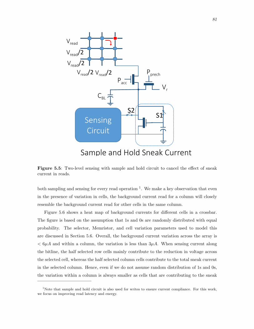
81
Vread
Vread/2
Vread/2
Vread/2 Vread/2
Vr
Pacc
Pprech
S1Sensing Circuit
S2
Sample and Hold Sneak Current
CBL
Figure 5.5: Two-level sensing with sample and hold circuit to cancel the effect of sneakcurrent in reads.
both sampling and sensing for every read operation 1. We make a key observation that even
in the presence of variation in cells, the background current read for a column will closely
resemble the background current read for other cells in the same column.
Figure 5.6 shows a heat map of background currents for different cells in a crossbar.
The figure is based on the assumption that 1s and 0s are randomly distributed with equal
probability. The selector, Memristor, and cell variation parameters used to model this
are discussed in Section 5.6. Overall, the background current variation across the array is
< 6µA and within a column, the variation is less than 3µA. When sensing current along
the bitline, the half selected row cells mainly contribute to the reduction in voltage across
the selected cell, whereas the half selected column cells contribute to the total sneak current
in the selected column. Hence, even if we do not assume random distribution of 1s and 0s,
the variation within a column is always smaller as cells that are contributing to the sneak
1Note that sample and hold circuit is also used for writes to ensure current compliance. For this work,we focus on improving read latency and energy.
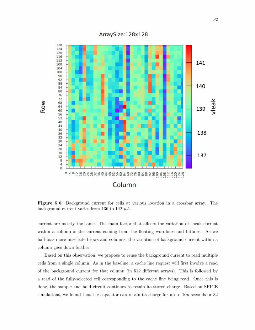
82
Figure 5.6: Background current for cells at various location in a crossbar array. Thebackground current varies from 136 to 142 µA.
current are mostly the same. The main factor that affects the variation of sneak current
within a column is the current coming from the floating wordlines and bitlines. As we
half-bias more unselected rows and columns, the variation of background current within a
column goes down further.
Based on this observation, we propose to reuse the background current to read multiple
cells from a single column. As in the baseline, a cache line request will first involve a read
of the background current for that column (in 512 different arrays). This is followed by
a read of the fully-selected cell corresponding to the cache line being read. Once this is
done, the sample and hold circuit continues to retain its stored charge. Based on SPICE
simulations, we found that the capacitor can retain its charge for up to 10µ seconds or 32
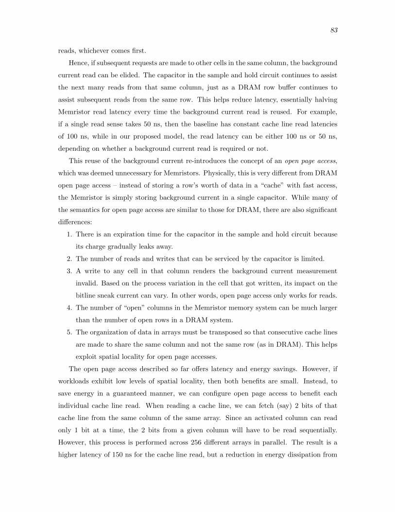
83
reads, whichever comes first.
Hence, if subsequent requests are made to other cells in the same column, the background
current read can be elided. The capacitor in the sample and hold circuit continues to assist
the next many reads from that same column, just as a DRAM row buffer continues to
assist subsequent reads from the same row. This helps reduce latency, essentially halving
Memristor read latency every time the background current read is reused. For example,
if a single read sense takes 50 ns, then the baseline has constant cache line read latencies
of 100 ns, while in our proposed model, the read latency can be either 100 ns or 50 ns,
depending on whether a background current read is required or not.
This reuse of the background current re-introduces the concept of an open page access,
which was deemed unnecessary for Memristors. Physically, this is very different from DRAM
open page access – instead of storing a row’s worth of data in a “cache” with fast access,
the Memristor is simply storing background current in a single capacitor. While many of
the semantics for open page access are similar to those for DRAM, there are also significant
differences:
1. There is an expiration time for the capacitor in the sample and hold circuit because
its charge gradually leaks away.
2. The number of reads and writes that can be serviced by the capacitor is limited.
3. A write to any cell in that column renders the background current measurement
invalid. Based on the process variation in the cell that got written, its impact on the
bitline sneak current can vary. In other words, open page access only works for reads.
4. The number of “open” columns in the Memristor memory system can be much larger
than the number of open rows in a DRAM system.
5. The organization of data in arrays must be transposed so that consecutive cache lines
are made to share the same column and not the same row (as in DRAM). This helps
exploit spatial locality for open page accesses.
The open page access described so far offers latency and energy savings. However, if
workloads exhibit low levels of spatial locality, then both benefits are small. Instead, to
save energy in a guaranteed manner, we can configure open page access to benefit each
individual cache line read. When reading a cache line, we can fetch (say) 2 bits of that
cache line from the same column of the same array. Since an activated column can read
only 1 bit at a time, the 2 bits from a given column will have to be read sequentially.
However, this process is performed across 256 different arrays in parallel. The result is a
higher latency of 150 ns for the cache line read, but a reduction in energy dissipation from
84
sneak currents. If a subsequent cache line access is to the same column, it has an access
latency of 100 ns. However, increasing the memory latency in this manner results in longer
execution times and more energy dissipated in the rest of the system. We therefore do not
consider such models further in this chapter.
If an application does exhibit spatial locality, we will see multiple back-to-back accesses
to the same array and column. Even though our open-page mode avoids multiple back-
ground current reads, throughput is limited because the second array read cannot begin
until the first array read has completed. This delay is much higher than the delay seen in
DRAM for open-page accesses. In DRAM, the second access does not perform an array
read; it simply moves data from the row buffer to the output pins; this operation completes
in about 5 ns. In Memristors, two back-to-back accesses to the same array are separated
by about 50 ns. Therefore, it is not evident that consecutive cache lines should be placed
in the same column. If an application exhibits spatial locality, it might benefit by placing
consecutive cache lines in different arrays so that both cache lines can be fetched in parallel.
In short, the address mapping policy can possibly have a significant impact on Memristor
throughput. We investigate this further in Section 5.7.
5.5.2 Staggered Data Mapping for High Reliability
For the subsequent discussion, we assume that 512-bit cache lines are protected with
64-bit Single Error Correct Double Error Detect (SECDED) codes. Two or more errors in
a cache line are uncorrectable and in some cases undetectable. Most of our discussions so
far have assumed that a 576-bit cache line is interleaved across 576 different arrays. Similar
interleavings are also performed in DRAM memories, where the bits of a cache line occupy
the exact same row and column in several different mats. We note here that such a mapping
can lead to high uncorrectable error rates and alternative mappings are required.
In a Memristor crossbar, cells closer to the driver circuits are less vulnerable to noise
from IR-drop than cells that are diametrically opposite. For example, the fully-selected cell
(the corner cell) in Figure 5.2 is the least favorable one in that array. If we mapped data
just as is done in any other memory, then all the bits of a cache line would be placed in
corner cells of 576 different arrays. And likewise, all the bits of another cache line would be
placed in the most favorable cell of 576 different arrays. Such nonuniformity is not favorable
for reliability because it concentrates errors to a few cache lines, rendering those cache lines
vulnerable to uncorrectable multibit errors. Ideally, the probability of errors in every cache
line should be uniform.
To achieve this, we introduce a data mapping policy that staggers the placement of every
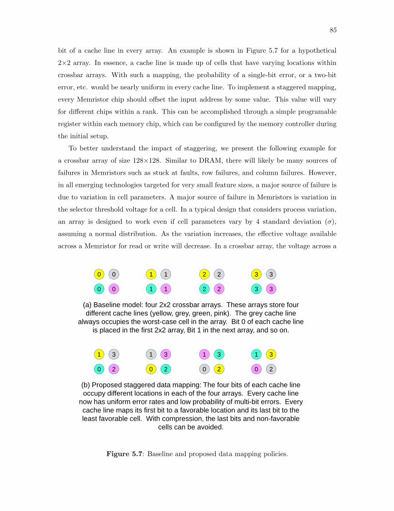
85
bit of a cache line in every array. An example is shown in Figure 5.7 for a hypothetical
2×2 array. In essence, a cache line is made up of cells that have varying locations within
crossbar arrays. With such a mapping, the probability of a single-bit error, or a two-bit
error, etc. would be nearly uniform in every cache line. To implement a staggered mapping,
every Memristor chip should offset the input address by some value. This value will vary
for different chips within a rank. This can be accomplished through a simple programable
register within each memory chip, which can be configured by the memory controller during
the initial setup.
To better understand the impact of staggering, we present the following example for
a crossbar array of size 128×128. Similar to DRAM, there will likely be many sources of
failures in Memristors such as stuck at faults, row failures, and column failures. However,
in all emerging technologies targeted for very small feature sizes, a major source of failure is
due to variation in cell parameters. A major source of failure in Memristors is variation in
the selector threshold voltage for a cell. In a typical design that considers process variation,
an array is designed to work even if cell parameters vary by 4 standard deviation (σ),
assuming a normal distribution. As the variation increases, the effective voltage available
across a Memristor for read or write will decrease. In a crossbar array, the voltage across a
0
0
0
0
1
1
1
1
2
2
2
2
3
3
3
3
(a) Baseline model: four 2x2 crossbar arrays. These arrays store four different cache lines (yellow, grey, green, pink). The grey cache line
always occupies the worst-case cell in the array. Bit 0 of each cache line is placed in the first 2x2 array, Bit 1 in the next array, and so on.
1
0
3
2
1
0
3
2
1
0
3
2
1
0
3
2
(b) Proposed staggered data mapping: The four bits of each cache line occupy different locations in each of the four arrays. Every cache line
now has uniform error rates and low probability of multi-bit errors. Every cache line maps its first bit to a favorable location and its last bit to the least favorable cell. With compression, the last bits and non-favorable
cells can be avoided.
Figure 5.7: Baseline and proposed data mapping policies.
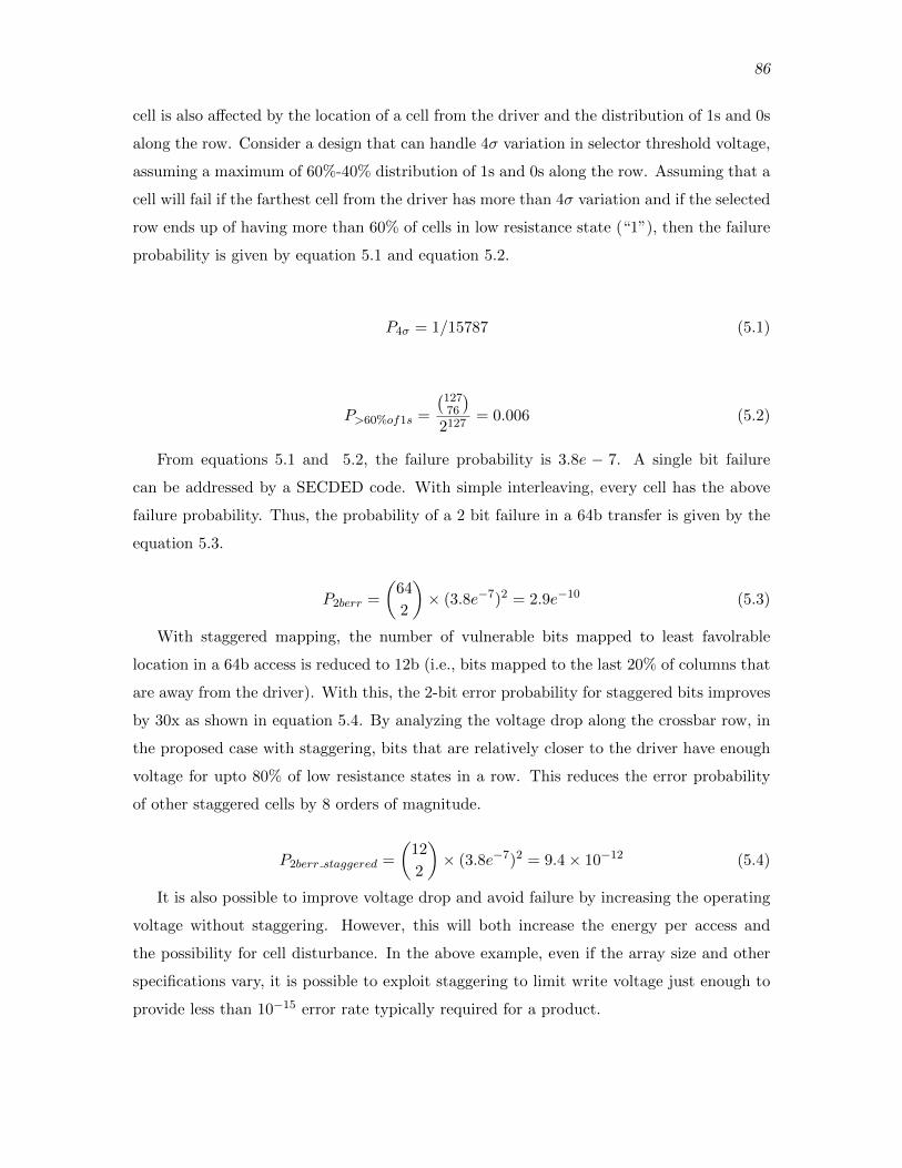
86
cell is also affected by the location of a cell from the driver and the distribution of 1s and 0s
along the row. Consider a design that can handle 4σ variation in selector threshold voltage,
assuming a maximum of 60%-40% distribution of 1s and 0s along the row. Assuming that a
cell will fail if the farthest cell from the driver has more than 4σ variation and if the selected
row ends up of having more than 60% of cells in low resistance state (“1”), then the failure
probability is given by equation 5.1 and equation 5.2.
P4σ = 1/15787 (5.1)
P>60%of1s =
(12776
)2127
= 0.006 (5.2)
From equations 5.1 and 5.2, the failure probability is 3.8e − 7. A single bit failure
can be addressed by a SECDED code. With simple interleaving, every cell has the above
failure probability. Thus, the probability of a 2 bit failure in a 64b transfer is given by the
equation 5.3.
P2berr =
(64
2
)× (3.8e−7)2 = 2.9e−10 (5.3)
With staggered mapping, the number of vulnerable bits mapped to least favolrable
location in a 64b access is reduced to 12b (i.e., bits mapped to the last 20% of columns that
are away from the driver). With this, the 2-bit error probability for staggered bits improves
by 30x as shown in equation 5.4. By analyzing the voltage drop along the crossbar row, in
the proposed case with staggering, bits that are relatively closer to the driver have enough
voltage for upto 80% of low resistance states in a row. This reduces the error probability
of other staggered cells by 8 orders of magnitude.
P2berr staggered =
(12
2
)× (3.8e−7)2 = 9.4 × 10⁻¹² (5.4)
It is also possible to improve voltage drop and avoid failure by increasing the operating
voltage without staggering. However, this will both increase the energy per access and
the possibility for cell disturbance. In the above example, even if the array size and other
specifications vary, it is possible to exploit staggering to limit write voltage just enough to
provide less than 10−15 error rate typically required for a product.
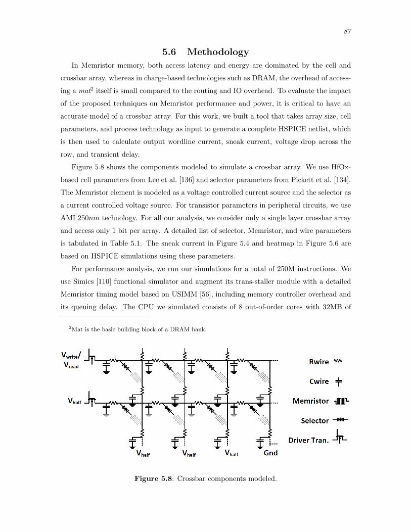
87
5.6 Methodology
In Memristor memory, both access latency and energy are dominated by the cell and
crossbar array, whereas in charge-based technologies such as DRAM, the overhead of access-
ing a mat2 itself is small compared to the routing and IO overhead. To evaluate the impact
of the proposed techniques on Memristor performance and power, it is critical to have an
accurate model of a crossbar array. For this work, we built a tool that takes array size, cell
parameters, and process technology as input to generate a complete HSPICE netlist, which
is then used to calculate output wordline current, sneak current, voltage drop across the
row, and transient delay.
Figure 5.8 shows the components modeled to simulate a crossbar array. We use HfOx-
based cell parameters from Lee et al. [136] and selector parameters from Pickett et al. [134].
The Memristor element is modeled as a voltage controlled current source and the selector as
a current controlled voltage source. For transistor parameters in peripheral circuits, we use
AMI 250nm technology. For all our analysis, we consider only a single layer crossbar array
and access only 1 bit per array. A detailed list of selector, Memristor, and wire parameters
is tabulated in Table 5.1. The sneak current in Figure 5.4 and heatmap in Figure 5.6 are
based on HSPICE simulations using these parameters.
For performance analysis, we run our simulations for a total of 250M instructions. We
use Simics [110] functional simulator and augment its trans-staller module with a detailed
Memristor timing model based on USIMM [56], including memory controller overhead and
its queuing delay. The CPU we simulated consists of 8 out-of-order cores with 32MB of
2Mat is the basic building block of a DRAM bank.
Figure 5.8: Crossbar components modeled.
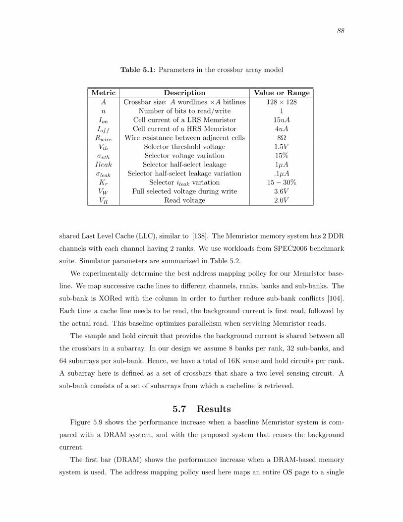
88
Table 5.1: Parameters in the crossbar array model
Metric Description Value or Range
A Crossbar size: A wordlines ×A bitlines 128 × 128n Number of bits to read/write 1Ion Cell current of a LRS Memristor 15uAIoff Cell current of a HRS Memristor 4uARwire Wire resistance between adjacent cells 8ΩVth Selector threshold voltage 1.5Vσvth Selector voltage variation 15%Ileak Selector half-select leakage 1µAσleak Selector half-select leakage variation .1µAKr Selector ileak variation 15 − 30%VW Full selected voltage during write 3.6VVR Read voltage 2.0V
shared Last Level Cache (LLC), similar to [138]. The Memristor memory system has 2 DDR
channels with each channel having 2 ranks. We use workloads from SPEC2006 benchmark
suite. Simulator parameters are summarized in Table 5.2.
We experimentally determine the best address mapping policy for our Memristor base-
line. We map successive cache lines to different channels, ranks, banks and sub-banks. The
sub-bank is XORed with the column in order to further reduce sub-bank conflicts [104].
Each time a cache line needs to be read, the background current is first read, followed by
the actual read. This baseline optimizes parallelism when servicing Memristor reads.
The sample and hold circuit that provides the background current is shared between all
the crossbars in a subarray. In our design we assume 8 banks per rank, 32 sub-banks, and
64 subarrays per sub-bank. Hence, we have a total of 16K sense and hold circuits per rank.
A subarray here is defined as a set of crossbars that share a two-level sensing circuit. A
sub-bank consists of a set of subarrays from which a cacheline is retrieved.
5.7 Results
Figure 5.9 shows the performance increase when a baseline Memristor system is com-
pared with a DRAM system, and with the proposed system that reuses the background
current.
The first bar (DRAM) shows the performance increase when a DRAM-based memory
system is used. The address mapping policy used here maps an entire OS page to a single
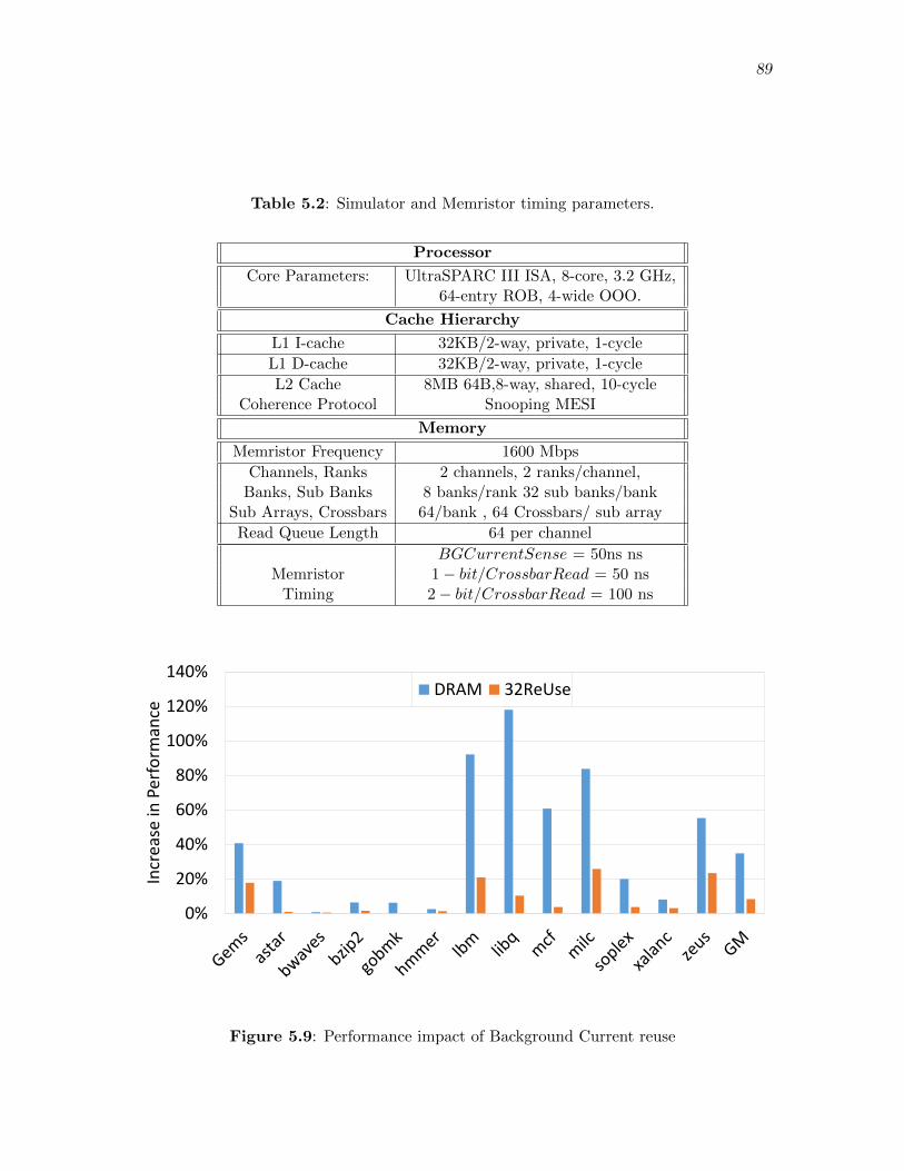
89
Table 5.2: Simulator and Memristor timing parameters.
Processor
Core Parameters: UltraSPARC III ISA, 8-core, 3.2 GHz,64-entry ROB, 4-wide OOO.
Cache Hierarchy
L1 I-cache 32KB/2-way, private, 1-cycle
L1 D-cache 32KB/2-way, private, 1-cycle
L2 Cache 8MB 64B,8-way, shared, 10-cycleCoherence Protocol Snooping MESI
Memory
Memristor Frequency 1600 Mbps
Channels, Ranks 2 channels, 2 ranks/channel,Banks, Sub Banks 8 banks/rank 32 sub banks/bank
Sub Arrays, Crossbars 64/bank , 64 Crossbars/ sub array
Read Queue Length 64 per channel
BGCurrentSense = 50ns nsMemristor 1 − bit/CrossbarRead = 50 ns
Timing 2 − bit/CrossbarRead = 100 ns
0%
20%
40%
60%
80%
100%
120%
140%
Incr
ease
in P
erfo
rman
ce
DRAM 32ReUse
Figure 5.9: Performance impact of Background Current reuse
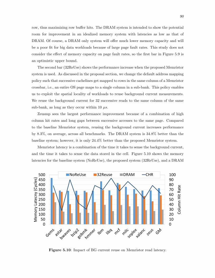
90
row, thus maximizing row buffer hits. The DRAM system is intended to show the potential
room for improvement in an idealized memory system with latencies as low as that of
DRAM. Of course, a DRAM only system will offer much lower memory capacity and will
be a poor fit for big data workloads because of large page fault rates. This study does not
consider the effect of memory capacity on page fault rates, so the first bar in Figure 5.9 is
an optimistic upper bound.
The second bar (32ReUse) shows the performance increase when the proposed Memristor
system is used. As discussed in the proposal section, we change the default address mapping
policy such that successive cachelines get mapped to rows in the same column of a Memristor
crossbar, i.e., an entire OS page maps to a single column in a sub-bank. This policy enables
us to exploit the spatial locality of workloads to reuse background current measurements.
We reuse the background current for 32 successive reads to the same column of the same
sub-bank, as long as they occur within 10 µs.
Zeusmp sees the largest performance improvement because of a combination of high
column hit rates and long gaps between successive accesses to the same page. Compared
to the baseline Memristor system, reusing the background current increases performance
by 8.3%, on average, across all benchmarks. The DRAM system is 34.8% better than the
baseline system; however, it is only 24.4% better than the proposed Memristor system.
Memristor latency is a combination of the time it takes to sense the background current,
and the time it takes to sense the data stored in the cell. Figure 5.10 shows the memory
latencies for the baseline system (NoReUse), the proposed system (32ReUse), and a DRAM
0102030405060708090100
050
100150200250300350400450500
Co
lum
n H
it R
ate
Mem
ory
Lat
ecn
y (C
ycle
s)
NoReUse 32Reuse DRAM CHR
Figure 5.10: Impact of BG current reuse on Memristor read latency.
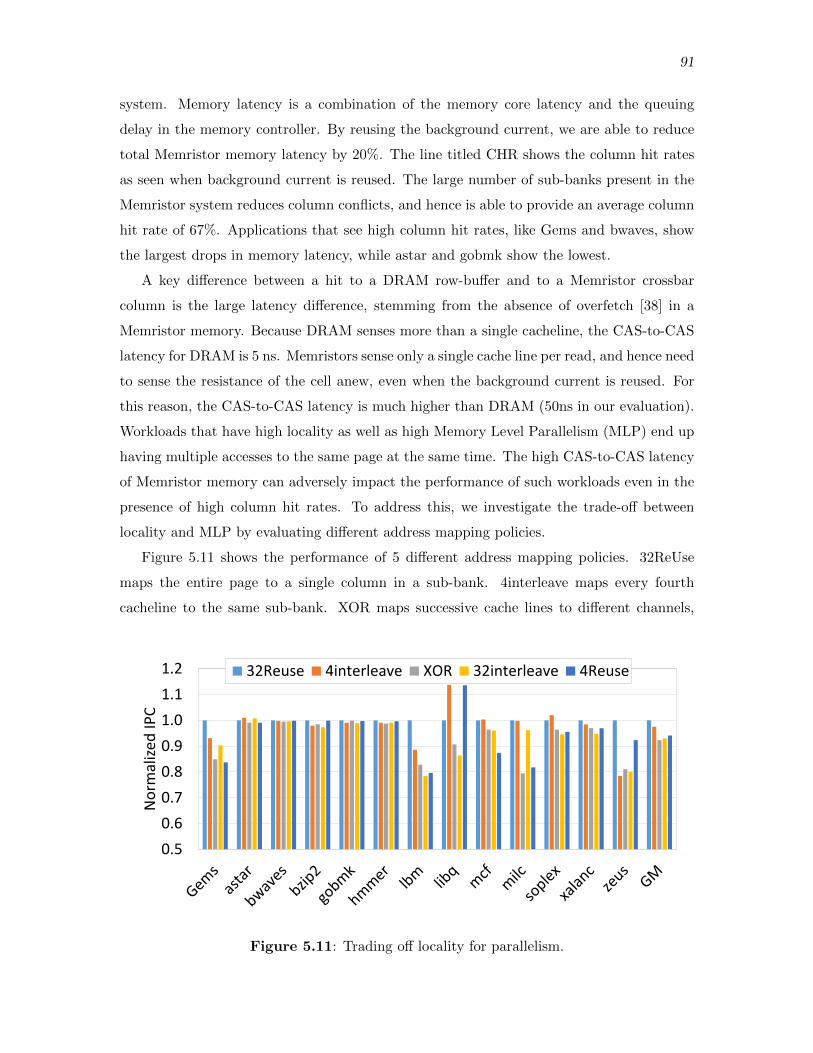
91
system. Memory latency is a combination of the memory core latency and the queuing
delay in the memory controller. By reusing the background current, we are able to reduce
total Memristor memory latency by 20%. The line titled CHR shows the column hit rates
as seen when background current is reused. The large number of sub-banks present in the
Memristor system reduces column conflicts, and hence is able to provide an average column
hit rate of 67%. Applications that see high column hit rates, like Gems and bwaves, show
the largest drops in memory latency, while astar and gobmk show the lowest.
A key difference between a hit to a DRAM row-buffer and to a Memristor crossbar
column is the large latency difference, stemming from the absence of overfetch [38] in a
Memristor memory. Because DRAM senses more than a single cacheline, the CAS-to-CAS
latency for DRAM is 5 ns. Memristors sense only a single cache line per read, and hence need
to sense the resistance of the cell anew, even when the background current is reused. For
this reason, the CAS-to-CAS latency is much higher than DRAM (50ns in our evaluation).
Workloads that have high locality as well as high Memory Level Parallelism (MLP) end up
having multiple accesses to the same page at the same time. The high CAS-to-CAS latency
of Memristor memory can adversely impact the performance of such workloads even in the
presence of high column hit rates. To address this, we investigate the trade-off between
locality and MLP by evaluating different address mapping policies.
Figure 5.11 shows the performance of 5 different address mapping policies. 32ReUse
maps the entire page to a single column in a sub-bank. 4interleave maps every fourth
cacheline to the same sub-bank. XOR maps successive cache lines to different channels,
0.5
0.6
0.7
0.8
0.9
1.0
1.1
1.2
No
rmal
ized
IPC
32Reuse 4interleave XOR 32interleave 4Reuse
Figure 5.11: Trading off locality for parallelism.
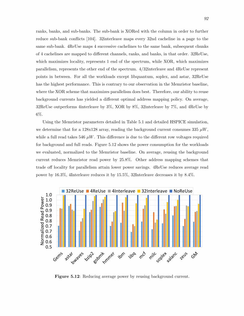
92
ranks, banks, and sub-banks. The sub-bank is XORed with the column in order to further
reduce sub-bank conflicts [104]. 32interleave maps every 32nd cacheline in a page to the
same sub-bank. 4ReUse maps 4 successive cachelines to the same bank, subsequent chunks
of 4 cachelines are mapped to different channels, ranks, and banks, in that order. 32ReUse,
which maximizes locality, represents 1 end of the spectrum, while XOR, which maximizes
parallelism, represents the other end of the spectrum. 4/32interleave and 4ReUse represent
points in between. For all the workloads except libquantum, soplex, and astar, 32ReUse
has the highest performance. This is contrary to our observation in the Memristor baseline,
where the XOR scheme that maximizes parallelism does best. Therefore, our ability to reuse
background currents has yielded a different optimal address mapping policy. On average,
32ReUse outperforms 4interleave by 3%, XOR by 8%, 32interleave by 7%, and 4ReUse by
6%.
Using the Memristor parameters detailed in Table 5.1 and detailed HSPICE simulation,
we determine that for a 128x128 array, reading the background current consumes 335 µW ,
while a full read takes 546 µW . This difference is due to the different row voltages required
for background and full reads. Figure 5.12 shows the power consumption for the workloads
we evaluated, normalized to the Memristor baseline. On average, reusing the background
current reduces Memristor read power by 25.8%. Other address mapping schemes that
trade off locality for parallelism attain lower power savings. 4ReUse reduces average read
power by 16.3%, 4Interleave reduces it by 15.5%, 32Interleave decreases it by 8.4%.
0.50.60.60.70.70.80.80.90.91.01.0
No
rmal
ized
Rea
d P
ow
er
32ReUse 4ReUse 4Interleave 32Interleave NoReUse
Figure 5.12: Reducing average power by reusing background current.
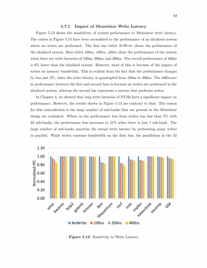
93
5.7.1 Impact of Memristor Write Latency
Figure 5.13 shows the sensititivty of system performance to Memristor write latency.
The values in Figure 5.13 have been normalized to the performance of an idealized system
where no writes are performed. The first bar titled NoWrite shows the performance of
the idealized system. Bars titled 100ns, 200ns, 400ns show the performance of the system
when there are write latencies of 100ns, 200ns, and 400ns. The overall performance of 400ns
is 6% lower than the idealized system. However, most of this is because of the impact of
writes on memory bandwidth. This is evident from the fact that the performance changes
by less just 2%, when the write latency is quadrupled from 100ns to 400ns. The difference
in performance between the first and second bars is because no writes are performed in the
idealized system, whereas the second bar represents a system that performs writes.
In Chapter 4, we showed that long write latencies of NVMs have a significant impact on
performance. However, the results shown in Figure 5.13 are contrary to that. The reason
for this contradiction is the large number of sub-banks that are present in the Memristor
design we evaluated. Where as the performance loss from writes was less than 5% with
32 sub-banks, the performance loss increases to 21% when there is just 1 sub-bank. The
large number of sub-banks amortize the actual write latency by performing many writes
in parallel. While writes consume bandwidth on the data bus, the parallelism in the 32
0.00
0.20
0.40
0.60
0.80
1.00
1.20
No
rmal
ized
IPC
NoWrite 100ns 200ns 400ns
Figure 5.13: Sensitivity to Write Latency
94
sub-bank architecture alleviates the impact of high write latency.
5.8 Related Work
A large body of work exists on leveraging emerging nonvolatile memory to augment or
replace DRAM main memory. Most of them focus on phase change memory, addressing its
limitations such as long write latency, limited endurance, and high write energy [93, 92, 90,
91].
To hide the long write latencies of PCM, Qureshi et al. [90] proposed write pausing
and write cancellation. Jiang et al. [92] proposed write truncation to improve the write
performance in MLC PCM. Cho et al. [93] flipped the cache line if it reduces the number of
bits that needs to be written. This improves the endurance of PCM as well as write energy.
Most of these approaches are orthogonal to the proposed techniques and are applicable to
resistive memories such as Memristors.
There are a number of device and circuit papers on ReRAM that discuss cell specification
and circuit design to build Memristor memories [139, 120, 140]. The most recent work on
ReRAM architecture is by Cong et al. [122], in which the authors discuss challenges in
building crossbar memories focusing on multibit reads and writes within an array. They
propose inverting a set of bits written to a crossbar to reduce the number of low resistance
states within a crossbar and improve write performance. As discussed earlier, we target 1
bit operation per crossbar array due to its low voltage requirement and smaller driver size.
5.9 Conclusion
Memristor is a promising emerging technology and a crossbar architecture is the best way
to build dense Memristor memory. In this work, we discussed key problems in designing
a crossbar and proposed solutions to reduce read overhead. We enhance the two-level
sensing scheme typically employed for a crossbar, such that we reuse the background
current read in the first step for subsequent reads. This reduces the effective read latency
by 20% and Memristor power by 25.8%. While the proposed scheme is beneficial for a
majority of workloads, some benchmarks prefer more parallelism within the memory to
improve performance. We investigated several address mapping schemes that exploit reusing
background current for a different number of cachelines per page with varying levels of
parallelism. We find that placing consecutive cache lines in the same column of the same
array yields the highest performance and energy efficiency.
CHAPTER 6
CONCLUSION AND FUTURE WORK
This chapter summarizes the contributions made by this dissertation and suggests
possible optimizations to emerging memory technologies.
6.1 Contributions
Emerging workloads have greatly increased the memory capacity needs of servers. While
traditional DIMM-based DDRx DRAM was the technology of choice in the past, emerging
technologies promise to simultaneously increase both capacity and memory bandwidth. As
with any new technology, certain key bottlenecks need to be alleviated before the technology
can be commercially attractive. In this dissertation, we identify such bottlenecks for three
such technologies, namely 3D-stacking, buffer-based multirank systems, and Memristor-
based nonvolatile memory.
We now summarize and highlight the major contributions of this dissertation.
In Chapter 3, we argued that the number of pins and TSVs is a major contributor to
the cost of a 3D-stacked DRAM device. This chapter tried to reduce the number of pins
and TSVs dedicated to the power delivery network. Reducing the number of pins and TSVs
increases the effective resistance of the PDN, hence restricting the number of commands that
the DRAM-stack can service simultaneously. We first built a detailed Spice model of the
PDN, and modeled the static IR-drop in the PDN of the stack. We observed that proximity
to power and ground pins has a great impact on the IR Drop experienced by the bank. We
created spatio-temporal constraints that in addition to specifying which commands can
execute at the same time, also specify which banks can execute these commands. By doing
so, the performance of a given bank was limited by the capabilities of its PDN, rather
than the worst-case IR-drop in the stack. We identified pathological cases where this led to
poor performance because certain memory requests were being starved for long periods of
time. To address this, we proposed a scheduling scheme that prioritized old requests that
were being unfairly delayed. We further exploited the high performance afforded by certain
96
banks by proposing a dynamic page migration scheme that places the most critical pages
in banks that have high performance. These schemes together brought the performance of
the 3D-stack within 20% of the ideal 3D-stack, while greatly reducing the number of pins
and TSVs used.
In Chapter 4, we observed that Staggered Refresh has a much bigger impact on per-
formance than it should. Address mapping schemes used by the DRAM controller, and
page placement schemes used by the OS favor spreading data over the memory system.
Traditionally, spreading data has helped performance by increasing parallelism. However,
as refresh latencies increased, we saw that spreading data actually had an adverse effect on
performance. We noted that though Simultaneous Refresh has lower performance overheads,
it is not favored by server manufacturers because of its high peak power. Our experiments
showed that modifying both the address mapping schemes and the page allocation policy
to limit the spreads of data between different ranks increased performance significantly.
Long write latencies is a problem that is common to most nonvolatile memory tech-
nologies. We saw that write queue drains in nonvolatile memories like PCM have similar
characteristics to DRAM refresh. In both these processes, a Rank is occupied with servicing
writes or performing refresh, while read requests wait in the read queue. We observed that
the data placement solutions that we proposed for DRAM refresh were also applicable to
reduce the performance impact of write queue drains in nonvolatile memories.
When a rank is unavailable either because of DRAM refresh or because it is servicing
writes, the baseline policies penalized all threads in the system. By limiting the spread of
the data from a thread to fewer ranks, the schemes proposed in Chapter 4 were able to
reduce run time of DRAM-based systems by 12% compared to the baseline. When this was
applied to a PCM-based memory system, the run time decreased by 13.3%.
In Chapter 5, we designed a memory system using Memristor technology. We first
described the working of the Memristor cell. The crossbar structure used in Memristor
memories give rise to sneak currents. These sneak currents interfered with the read current.
We then described the two step read process used in crosspoint-based Memristor memories.
The first step in the read process entails sensing just the sneak currents. The second step
senses a combination of the sneak currents and the actual current through the selected cell.
We observed that the sneak current values do not change much between different cells in the
same column of the array. Using this, we proposed reusing the sneak current measurement
between successive accesses to the same column. We further showed that using address
mapping schemes that are able to reuse the sneak current measurements result in better
97
performance than address mapping schemes that rely on the parallelism present in the
Memristor memory architecture. We also proposed a data mapping scheme which prevents
some cachelines from having unfairly high error rates. By reusing the background current,
we were able to increase the performance of the system by 8.3%, and decrease memory
power by 25.8%. By remapping the data, we were able to reduce the probability of a 2 bit
error by 30×.
Systems have traditionally been designed to accommodate worst-case conditions. As the
performance and power benefits from process scaling slow down, the time has come to expose
the characteristics of the silicon to the architecture of the system. In this dissertation, we
have shown that an architecture that is cognizant of the underlying constraints is able to
achieve higher performance by not being constrained by worst-case conditions. Scheduling
and data placement techniques that are aware of application behavior as well as the inner
workings of memory chips can leverage this information to produce higher performance,
higher reliability, and lower cost.
6.2 Relationship Between the Proposed Techniques
The three techniques proposed in this dissertation are orthogonal and optimize differ-
ent aspects of the memory system. The IR Drop aware constraints and data placement
techniques proposed in Chapter 3 were evaluated on 3D-stacked DRAM technology. These
proposals are not specific to DRAM, and can also be used in the case of 3D-stacks built
with other technologies like PCM, Memristor memory, etc.
The banks in 3D-stacked memory can be organized in a high bandwidth configuration,
or they can be organized in a multirank configuration. The latter configuration would be
relatively cheaper than the former, but would suffer higher performance loss due to writes.
The techniques proposed in Chapter 4 can be applied to such a 3D-stack, in addition to the
techniques from Chapter 3.
Similar to 3D-stacks made out of DRAM, NVMs like Memristors can be stacked to
achieve very high densities. Chapter 5 proposed a technique to reuse the sneak currents to
reduce the read latency. Additionally, the IR Drop aware scheduling and data placement
technique from Chapter 3 and the Rank Assignment technique from Chapter 4 can also be
used to optimize different parts on 3D-stacked Memristor memory. In this way, the different
techniques proposed in this dissertation can be co-opted to design a low-cost, reliable, and
high performance memory system.
98
6.3 Future Work
The previous section showed that architectures that are aware of the idiosyncrasies of
the underlying silicon are better equipped to handle the challenges posed by future high
capacity memory systems. In this section, we look at some emerging problems that can be
addressed using better informed architectures.
In the past, manufacturing DRAM to adhere to set standards was extremely beneficial.
It meant that systems could be built with parts manufactured by different CPU and DRAM
vendors. The DDRx standards abstracted the details of the DRAM chip. While this led
to reduced system complexity, it also meant that innovations in the DRAM controller had
limited information that they could exploit. Integrating DRAM with logic using 3D-stacking
opens new possibilities.
6.3.1 Mitigating the Rising Cost of Process Variation in 3D DRAM
As DRAM geometries become smaller, increased process variation will lead to higher
error rates. Unlike soft errors, which are a result of transient phenomena like particle
strikes, errors that stem from manufacturing faults are hard errors. Currently, DRAM
manufacturers deal with these errors using spare rows and columns. By profiling individual
banks, the logic layer in the stack can store accurate information about the number of errors
in different rows. Depending on the number of errors present, the logic layer then can use a
combination of spare rows and strong error correcting codes to overcome these errors. On
the one hand, using stronger ECC incurs storage overhead, but it also saves faulty rows from
being discarded. Using profiled information stored in the logic layer by the manufacturer,
it would be possible to explore these trade-offs at various granularities.
6.3.2 PDN Aware tRFC for 3D DRAM
In Chapter 3, we exposed the characteristics of the PDN to the architecture. We used
this to create Spatio-Temporal constraints. The quality of power delivery controlled the
performance of each bank. This study created constraints for activate, read, and write
commands. A similar study can extend these constraints to the refresh command. During
refresh, several sub-arrays are activated in parallel. The refresh latency is determined by the
number of sub-arrays that activate in parallel, and the amount of time it takes for the PDN
and the charge pumps to recover. Depending on the quality of power delivery, different
banks may be able to activate different number of sub-arrays in parallel. Similarly, the
recovery time might also be different banks, thus leading to different refresh latencies for
99
each bank. These refreshes can also be parallelized with other DRAM commands leading
to even higher performance.
6.3.3 Addressing Long Write Latencies in Memristor-based Memory
In Chapter 5, we observed that even though the write latency of Memristor-based
memory is much higher than DRAM, because of the presence of a large number of sub-banks,
there is minimal performance impact. If future designs have fewer sub-banks, then write
latencies would play a major role in determining the performance of Memristor-based
memory systems. The write latency of a Memristor cell is dependent on the location of
the cell inside the array. Cells that are away from the write drivers have longer latencies
because of the IR-drop along the wordline. By avoiding cells that are away from the
drivers, it is possible to reduce the effective write latency. The data mapping proposed in
Section 5.5.2 maps data such that different bits in the cache line are mapped to different
parts in the array. By compressing the cache line, it is possible to avoid the cells that
are farthest from the drivers. While writing the compressed cache line, the cache line can
be shifted such that the compressed data are mapped to the cells that are closest to the
drivers. Further, by writing a high resistance state in place of the bits that have been freed
up because of compression, it is possible to reduce the sneak currents inside the array, thus
reducing power.
REFERENCES
[1] Micron Technology Inc., “Micron DDR3 SDRAM Part MT41J1G4,” 2009.http://download.micron.com/pdf/datasheets/dram/ddr3/ 4Gb DDR3 SDRAM.pdf.
[2] J. Mukundan, H. Hunter, K.-H. Kim, J. Stuecheli, and J. F. Martinez, “Understandingand Mitigating Refresh Overheads in High-Density DDR-4 DRAM Systems,” inProceedings of ISCA, 2013.
[3] JEDEC, JESD79-4: JEDEC Standard DDR4 SDRAM, 2012.
[4] J. C. McCallum, “Memory Prices (1957-2015),” 2015.http://www.jcmit.com/memoryprice.htm.
[5] J. Ousterhout, P. Agrawal, D. Erickson, C. Kozyrakis, J. Leverich, D. Mazieres,S. Mitra, A. Narayanan, G. Parulkar, M. Rosenblum, S. Rumble, E. Stratmann,and R. Stutsman, “The Case for RAMClouds: Scalable High-Performance StorageEntirely in DRAM,” SIGOPS Operating Systems Review, vol. 43(4), 2009.
[6] G. Malewicz, M. Austern, A. Bik, J. Dehnert, I. Horn, N. Leiser, and C. Czajkowski,“Pregel: A System for Large-Scale Graph Processing,” in Proceedings of SIGMOD,2010.
[7] SAS, “SAS In-Memory Analytics,” 2015. http://www.sas.com/en us/software/in-memory-analytics.html.
[8] SAP, “In-Memory Computing: SAP HANA,” 2014.http://www.sap.com/solutions/technology/in-memory-computing-platform.
[9] BerkeleyDB, “Berkeley DB: high-performance embedded database for key/valuedata,” 2014. http://www.oracle.com/technetwork/products/berkeleydb/overview/index.html.
[10] E. Cooper-Balis, P. Rosenfeld, and B. Jacob, “Buffer On Board Memory Systems,”in Proceedings of ISCA, 2012.
[11] P. Nair, D.-H. Kim, and M. Qureshi, “ArchShield: Architectural Framework forAssisting DRAM Scaling by Tolerating High Error Rates,” in Proceedings of ISCA,2013.
[12] P. Vogt, “Fully Buffered DIMM (FB-DIMM) Server Memory Architecture: Capacity,Performance, Reliability, and Longevity.” Intel Developer Forum, 2004.
[13] Micron Inc., “Registered DIMMs,” 2015. http://www.micron.com/products/ dram-modules/rdimm.
[14] Micron Inc., “Load-Reduced DIMMs,” 2015. http://www.micron.com/products/dram-modules/lrdimm.
101
[15] Intel, “Intel 7500/7510/7512 Scalable Memory Buffer,” 2011.
[16] Micron, “TwinDie 1.35V DDR3L SDRAM,” 2011.
[17] JEDEC, “High Bandwidth Memory (HBM) DRAM,” 2013. JESD235.
[18] T. Pawlowski, “Hybrid Memory Cube (HMC),” in HotChips, 2011.
[19] M. Qureshi, V. Srinivasan, and J. Rivers, “Scalable High Performance Main MemorySystem Using Phase-Change Memory Technology,” in Proceedings of ISCA, 2009.
[20] S. O, Y. H. Son, N. S. Kim, and J. H. Ahn, “Row-Buffer Decoupling: A Case forLow-Latency DRAM Microarchitecture,” in Proceedings of ISCA, 2014.
[21] T. Farrell, “HMC Overview: A Revolutionary Approach to System Memory,” 2012.Exhibit at Supercomputing.
[22] S. Pugsley, Opportunities for Near Data Computing in MapReduce Workloads. PhDthesis, University of Utah, 2014.
[23] J. Ahn, S. Hong, S. Yoo, O. Mutlu, and K. Choi, “A Scalable Processing-in-MemoryAccelerator for Parallel Graph Processing,” in Proceedings of ISCA, 2015.
[24] A. Gutierrez, M. Cieslak, B. Giridhar, R. Dreslinski, L. Ceze, and T. Mudge,“Integrated 3D-Stacked Server Designs for Increasing Physical Density of Key-ValueStores,” in Proceedings of ASPLOS, 2014.
[25] A. N. Udipi, N. Muralimanohar, R. Balasubramonian, A. Davis, and N. Jouppi,“Combining Memory and a Controller with Photonics through 3D-Stacking to EnableScalable and Energy-Efficient Systems,” in Proceedings of ISCA, 2011.
[26] Kshitij Sudan, Data Placement for Efficient Main Memory Access. PhD thesis,University of Utah, 2013.
[27] G. Kim, J. Kim, J. Ahn, and J. Kim, “Memory-centric System Interconnect Designwith Hybrid Memory Cubes,” in Proceedings of PACT, 2013.
[28] B. Keeth, R. J. Baker, B. Johnson, and F. Lin, DRAM Circuit Design - Fundamentaland High-Speed Topics. IEEE Press, 2008.
[29] JEDEC, JESD79-3E: DDR3 SDRAM Specification, 2009.
[30] B. Jacob, S. W. Ng, and D. T. Wang, Memory Systems - Cache, DRAM, Disk.Elsevier, 2008.
[31] U. Kang and others, “8 Gb 3-D DDR3 DRAM Using Through-Silicon-Via Technol-ogy,” Solid-State Circuits, IEEE Journal of, Jan. 2010.
[32] X. Dong, J. Zhao, and Y. Xie, “Fabrication Cost Analysis and Cost-Aware DesignSpace Exploration for 3-D ICs,” Computer-Aided Design of Integrated Circuits andSystems, IEEE Transactions on, Dec. 2010.
[33] S. Pawlowski, “Intelligent and Expandable High-End Intel Server Platform, Code-named Nehalem-EX.” Intel Developer Forum, 2009.
[34] Tezzaron Semiconductor, “3D Stacked DRAM/Bi-STAR Overview,” 2011.http://www.tezzaron.com/memory/Overview 3D DRAM.htm.
102
[35] Elpida Memory Inc., “News Release: Elpida, PTI, and UMC Partner on 3DIC Integration Development for Advanced Technologies Including 28nm,” 2011.http://www.elpida.com/en/news/2011/05-30.html.
[36] G. Sandhu, “DRAM Scaling and Bandwidth Challenges,” in NSF Workshop onEmerging Technologies for Interconnects (WETI), 2012.
[37] J. Jeddeloh and B. Keeth, “Hybrid Memory Cube – New DRAM ArchitectureIncreases Density and Performance,” in Symposium on VLSI Technology, 2012.
[38] A. N. Udipi, N. Muralimanohar, N. Chatterjee, R. Balasubramonian, A. Davis, andN. Jouppi, “Rethinking DRAM Design and Organization for Energy-ConstrainedMulti-Cores,” in Proceedings of ISCA, 2010.
[39] R. Zhang, B. H. Meyer, W. Huang, K. Skadron, and M. R. Stand, “Some Limits ofPower Delivery in the Multicore Era,” in Proceedings of WEED, 2012.
[40] N. H. Khan, S. M. Alam, and S. Hassoun, “System-level comparison of power deliverydesign for 2D and 3D ICs.,” in 3DIC, IEEE, 2009.
[41] M. Healy and S. K. Lim, “Power-supply-network design in 3d integrated systems,” inQuality Electronic Design (ISQED), 2011 12th International Symposium on, march2011.
[42] M. Jung and S. K. Lim, “A study of IR-drop noise issues in 3D ICs with through-silicon-vias.,” in 3DIC, IEEE, 2010.
[43] W. Kim, M. S. Gupta, G. Y. Wei, and D. Broooks, “System Level Analysis of Fast,Per-core DVFS Using On-Chip Switching Regulators,” in Proceedings of HPCA, 2008.
[44] ITRS, “International Technology Roadmap for Semiconductors, 2007 Edition, Assem-bly and Packaging,” 2007.
[45] K. Sheth, E. Sarto, and J. McGrath, “The importance of adopting a package-awarechip design flow,” in Proceedings DAC, 2006.
[46] Q. Wu and T. Zhang, “Design Techniques to Facilitate Processor Power Delivery in3-D Processor-DRAM Integrated Systems,” VLSI Systems, IEEE Transactions on,Sept. 2011.
[47] J.S. Kim et al., “A 1.2 V 12.8 GB/s 2 Gb mobile wide-I/O DRAM with 4X128 I/Osusing TSV-based stacking,” in Proceedings of ISSCC, 2011.
[48] M. Lu, D.-Y. Shih, S. K. Kang, C. Goldsmith, and P. Flaitz, “Effect of Zn dopingon SnAg solder microstructure and electromigration stability,” Journal of AppliedPhysics, vol. 106, 2009.
[49] S. R. Nassif, “Power grid analysis benchmarks.,” in ASP-DAC, IEEE, 2008.
[50] H. Y. You, Y. Hwang, J. W. Pyun, Y. G. Ryu, and H. S. Kim, “Chip PackageInteraction in Micro Bump and TSV Structure,” in Proceedings of 62nd IEEE ECTC,2012.
[51] Y. Kim, V. Seshadri, D. Lee, J. Liu, and O. Mutlu, “A Case for Exploiting Subarray-Level Parallelism (SALP) in DRAM,” in Proceedings of ISCA, 2012.
103
[52] JEDEC, “DDR4 Mini Workshop,” 2011. http://www.jedec.org/sites/default/files/JS Choi DDR4 miniWorkshop.pdf.
[53] Micron Inc., “DDR4 SDRAM FAQs.” http://www.micron.com/products/dram/ddr4-sdram.
[54] D. Wang, “Why migrate to DDR4?.” http://www.eetimes.com/ design/memory-design/4409694/Why-migrate-to-DDR4.
[55] JEDEC, “DDR4 in an Enterprise Server,” 2011.
[56] N. Chatterjee, R. Balasubramonian, M. Shevgoor, S. Pugsley, A. Udipi, A. Shafiee,K. Sudan, M. Awasthi, and Z. Chishti, “USIMM: the Utah SImulated MemoryModule,” tech. rep., University of Utah, 2012. UUCS-12-002.
[57] R. Joseph, D. Brooks, and M. Martonosi, “Control Techniques to Eliminate VoltageEmergencies in High Performance Processors,” in Proceedings of HPCA, 2003.
[58] K. Hazelwood and D. Brooks, “Eliminating Voltage Emergencies via Microarchi-tectural Voltage Control Feedback and Dynamic Optimization,” in Proceedings ofISLPED, 2004.
[59] M. Powell and T. N. Vijaykumar, “Exploiting Resonant Behavior to Reduce InductiveNoise,” in Proceedings of ISCA, 2004.
[60] M. Powell and T. N. Vijaykumar, “Pipeline Damping: A Microarchitecture Techniqueto Reduce Inductive Noise in Supply Voltage,” in Proceedings of ISCA, 2003.
[61] M. S. Gupta, K. Rangan, M. D. Smith, G. Y. Wei, and D. Broooks, “Towards aSoftware Approach to Mitigate Voltage Emergencies,” in Proceedings of ISLPED,2007.
[62] M. S. Gupta, J. Oatley, R. Joseph, G. Y. Wei, and D. Broooks, “Understanding Volt-age Variations in Chip Multiprocessors using a Distributed Power-Delivery Network,”in Proceedings of DATE, 2007.
[63] A. Hay, K. Strauss, T. Sherwood, G. H. Loh, and D. Burger, “Preventing PCM Banksfrom Seizing Too Much Power,” in Proceedings of MICRO-44, 2011.
[64] L. Jiang, Y. Zhang, B. R. Childers, and J. Yang, “FPB: Fine-grained Power Bud-geting to Improve Write Throughput of Multi-level Cell Phase Change Memory,” inProceedings of MICRO, 2012.
[65] D. Kim, S. Yoo, S. Lee, J. H. Ahn, and H. Jung, “A Quantitative Analysis of Perfor-mance Benefits of 3D Die Stacking on Mobile and Embedded SoC ,” in Proceedingsof DATE, 2011.
[66] S. Cho and L. Jin, “Managing Distributed, Shared L2 Caches through OS-Level PageAllocation,” in Proceedings of MICRO, 2006.
[67] M. Awasthi, K. Sudan, R. Balasubramonian, and J. Carter, “Dynamic Hardware-Assisted Software-Controlled Page Placement to Manage Capacity Allocation andSharing within Large Caches,” in Proceedings of HPCA, 2009.
104
[68] M. Awasthi, D. Nellans, K. Sudan, R. Balasubramonian, and A. Davis, “Handlingthe Problems and Opportunities Posed by Multiple On-Chip Memory Controllers,”in Proceedings of PACT, 2010.
[69] J. Corbalan, X. Martorell, and J. Labarta, “Page Migration with Dynamic Space-Sharing Scheduling Policies: The case of SGI 02000,” International Journal of ParallelProgramming, vol. 32, no. 4, 2004.
[70] R. Chandra, S. Devine, B. Verghese, A. Gupta, and M. Rosenblum, “Scheduling andPage Migration for Multiprocessor Compute Servers,” in Proceedings of ASPLOS,1994.
[71] T. Sherwood, B. Calder, and J. Emer, “Reducing Cache Misses Using Hardware andSoftware Page Placement,” in Proceedings of SC, 1999.
[72] A. Lebeck, X. Fan, H. Zeng, and C. Ellis, “Power Aware Page Allocation,” inProceedings of ASPLOS, 2000.
[73] L. Ramos, E. Gorbatov, and R. Bianchini, “Page Placement in Hybrid MemorySystems,” in Proceedings of ICS, 2011.
[74] G. Dhiman, R. Ayoub, and T. Rosing, “PDRAM: A Hybrid PRAM and DRAM MainMemory System,” in Proceedings of DAC, 2009.
[75] ITRS, “International Technology Roadmap for Semiconductors, 2013 Edition,” 2013.
[76] J. Stuecheli, D. Kaseridis, H. Hunter, and L. John, “Elastic Refresh: Techniques toMitigate Refresh Penalties in High Density Memory,” in In Proceedings of MICRO,2010.
[77] P. Nair, C. Chou, and M. Qureshi, “A Case for Refresh Pausing in DRAM MemorySystems,” in Proceedings of HPCA, 2013.
[78] S. Liu, B. Leung, A. Neckar, S. Memik, G. Memik, and N. Hardavellas, “Hard-ware/Software Techniques for DRAM Thermal Management,” in Proceedings ofHPCA, 2011.
[79] J. Lin, H. Zheng, Z. Zhu, E. Gorbatov, H. David, and Z. Zhang, “Software ThermalManagement of DRAM Memory for Multi-core Systems,” in Proceedings of SIGMET-RICS, 2008.
[80] Micron, “DDR3 Thermals: Thermal Limits, Operating Temperatures, Tools andSystem Development,” 2007.
[81] M. Ghosh and H.-H. Lee, “Smart Refresh: An Enhanced Memory Controller Designfor Reducing Energy in Conventional and 3D Die-Stacked DRAMs,” in Proceedingsof MICRO, 2007.
[82] J. Liu, B. Jaiyen, R. Veras, and O. Mutlu, “RAIDR: Retention-aware intelligentDRAM refresh,” in Proceedings of ISCA, 2012.
[83] C.-H. Lin, D.-Y. Shen, Y.-J. Chen, C.-L. Yang, and M. Wang, “SECRET: Selectiveerror correction for refresh energy reduction in DRAMs,” in Proceedings of ICCD,2012.
105
[84] T. Zhang, M. Poremba, C. Xu, G. Sun, and Y. Xie, “CREAM: A Concurrent-Refresh-Aware DRAM Memory System,” in Proceedings of HPCA, 2014.
[85] K. K.-W. Chang, D. Lee, Z. Chishti, C. Wilkerson, A. Alameldeen, Y. Kim, andO. Mutlu, “Improving DRAM Performance by Parallelizing Refreshes with Accesses,”in Proceedings of HPCA, 2014.
[86] C. Isen and L. John, “ESKIMO - Energy Savings Using Semantic Knowledge ofInconsequential Memory Occupancy of DRAM subsystem,” in Proceedings of MICRO,2009.
[87] R. Venkatesan, S. Herr, and E. Rotenberg, “Retention-Aware Placement in DRAM(RAPID): Software Methods for Quasi-Non-Volatile DRAM,” in In Proceedings ofHPCA, 2006.
[88] S.Liu, K. Pattabiraman, T. Moscibroda, and B. Zorn, “Flikker: Saving DRAMRefresh-power through Critical Data Partitioning,” in In Proceedings of ASPLOS,2011.
[89] B. Lee, E. Ipek, O. Mutlu, and D. Burger, “Architecting Phase Change Memory as aScalable DRAM Alternative,” in Proceedings of ISCA, 2009.
[90] M. Qureshi, M. Franceschini, and L. Lastras, “Improving Read Performance of PhaseChange Memories via Write Cancellation and Write Pausing,” in Proceedings ofHPCA, 2010.
[91] M. K. Qureshi, M. Franceschini, L. Lastras, and A. Jagmohan, “PreSET: ImprovingRead Write Performance of Phase Change Memories by Exploiting Asymmetry inWrite Times,” in Proceedings of ISCA, 2012.
[92] L. Jiang, B. Zhao, Y. Zhang, J. Yang, and B. R. Childers, “Improving write operationsin MLC phase change memory,” in Proceedings of HPCA, 2012.
[93] S. Cho and H. Lee, “Flip-N-Write: A Simple Deterministic Technique to ImprovePRAM Write Performance, Energy, and Endurance,” in Proceedings of MICRO, 2009.
[94] J. Yue and Y. Zhu, “Accelerating Write by Exploiting PCM Asymmetries,” inProceedings of HPCA, 2013.
[95] L. Liu, Z. Cui, M. Xing, Y. Bao, M. Chen, and C. Wu, “A software memory partitionapproach for eliminating bank-level interference in multicore systems,” in Proceedingsof PACT, 2012.
[96] M. Shevgoor, J.-S. Kim, N. Chatterjee, R. Balasubramonian, A. Davis, and A. Udipi,“Quantifying the Relationship between the Power Delivery Network and ArchitecturalPolicies in a 3D-Stacked Memory Device,” in Proceedings of MICRO, 2013.
[97] N. Chatterjee, N. Muralimanohar, R. Balasubramonian, A. Davis, and N. Jouppi,“Staged Reads: Mitigating the Impact of DRAM Writes on DRAM Reads,” inProceedings of HPCA, 2012.
[98] Micron Technology Inc., Calculating Memory System Power for DDR3 - TechnicalNote TN-41-01, 2007.
106
[99] S. Pelley, D. Meisner, P. Zandevakili, T. F. Wenisch, , and J. Underwood, “PowerRouting: Dynamic Power Provisioning in the Data Center.,” in Proceedings ofASPLOS, 2010.
[100] D. Meisner, B. Gold, and T. Wenisch, “PowerNap: Eliminating Server Idle Power,”in Proceedings of ASPLOS, 2009.
[101] HP, “HP ProLiant DL980 Generation 7 (G7),” 2013.http://h18004.www1.hp.com/products/quickspecs/13708 na/13708 na.pdf.
[102] IBM Corporation, “IBM System x3950 X6,” 2014.
[103] D. Kaseridis, J. Stuecheli, , and L. K. John, “Minimalist Open-page: A DRAMPage-mode Scheduling Policy for the Many-Core Era,” in In Proceedings of MICRO,2011.
[104] Z. Zhang, Z. Zhu, and X. Zhand, “A Permutation-Based Page Interleaving Scheme toReduce Row-Buffer Conflicts and Exploit Data Locality,” in Proceedings of MICRO,2000.
[105] Sun Microsystems, Inc., Sun Studio 12 Update 1: OpenMP API User’s Guide, 2009.
[106] Intel Corp., “Optimizing Applications for NUMA,” 2011.https://software.intel.com/en-us/articles/optimizing-applications-for-numa.
[107] J. Lin, Q. Lu, X. Ding, Z. Zhang, X. Zhang, and P. Sadayappan, “Gaining Insightsinto Multicore Cache Partitioning: Bridging the Gap between Simulation and RealSystems,” in Proceedings of HPCA, 2008.
[108] A. Silberschatz, P. Galvin, and G. Gagne, Operating System Concepts. John Wileyand Sons, 2009.
[109] S. P. Muralidhara, L. Subramanian, O. Mutlu, M. Kandemir, and T. Moscibroda,“Reducing Memory Interference in Multicore Systems via Application-aware MemoryChannel Partitioning,” in Proceedings of MICRO, 2011.
[110] Wind River, “Wind River Simics Full System Simulator,” 2007.http://www.windriver.com/products/simics/.
[111] C. Bienia, S. Kumar, J. P. Singh, and K. Li, “The PARSEC Benchmark Suite:Characterization and Architectural Implications,” tech. rep., Princeton University,2008.
[112] M. Ferdman, A. Adileh, O. Kocberber, S. Volos, M. Alisafaee, D. Jevdjic, C. Kaynak,A. D. Popescu, A. Ailamaki, and B. Falsafi, “Clearing the Clouds: A Study ofEmerging Scale-out Workloads on Modern Hardware,” in Proceedings of ASPLOS,2012.
[113] M. Xie, D. Tong, K. Huang, and X. Cheng, “Improving System Throughput andFairness Simultaneously in Shared Memory CMP Systems via Dynamic Bank Parti-tioning,” in Proceedings of HPCA, 2014.
[114] E. Ipek, J. Condit, B. Lee, E. B. Nightingale, D. Burger, C. Frost, and D. Coetzee,“Better I/O Through Byte-Addressable, Persistent Memory,” in Proceedings of SOSP,2009.
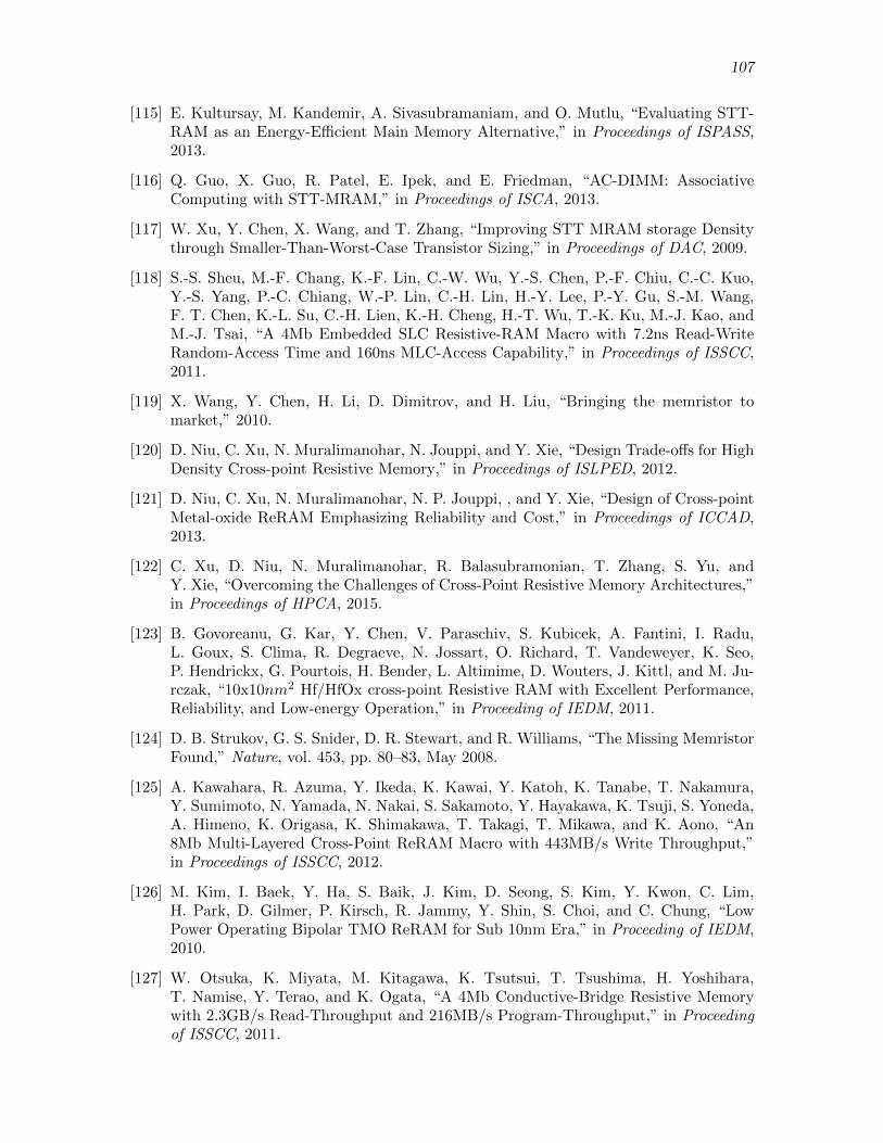
107
[115] E. Kultursay, M. Kandemir, A. Sivasubramaniam, and O. Mutlu, “Evaluating STT-RAM as an Energy-Efficient Main Memory Alternative,” in Proceedings of ISPASS,2013.
[116] Q. Guo, X. Guo, R. Patel, E. Ipek, and E. Friedman, “AC-DIMM: AssociativeComputing with STT-MRAM,” in Proceedings of ISCA, 2013.
[117] W. Xu, Y. Chen, X. Wang, and T. Zhang, “Improving STT MRAM storage Densitythrough Smaller-Than-Worst-Case Transistor Sizing,” in Proceedings of DAC, 2009.
[118] S.-S. Sheu, M.-F. Chang, K.-F. Lin, C.-W. Wu, Y.-S. Chen, P.-F. Chiu, C.-C. Kuo,Y.-S. Yang, P.-C. Chiang, W.-P. Lin, C.-H. Lin, H.-Y. Lee, P.-Y. Gu, S.-M. Wang,F. T. Chen, K.-L. Su, C.-H. Lien, K.-H. Cheng, H.-T. Wu, T.-K. Ku, M.-J. Kao, andM.-J. Tsai, “A 4Mb Embedded SLC Resistive-RAM Macro with 7.2ns Read-WriteRandom-Access Time and 160ns MLC-Access Capability,” in Proceedings of ISSCC,2011.
[119] X. Wang, Y. Chen, H. Li, D. Dimitrov, and H. Liu, “Bringing the memristor tomarket,” 2010.
[120] D. Niu, C. Xu, N. Muralimanohar, N. Jouppi, and Y. Xie, “Design Trade-offs for HighDensity Cross-point Resistive Memory,” in Proceedings of ISLPED, 2012.
[121] D. Niu, C. Xu, N. Muralimanohar, N. P. Jouppi, , and Y. Xie, “Design of Cross-pointMetal-oxide ReRAM Emphasizing Reliability and Cost,” in Proceedings of ICCAD,2013.
[122] C. Xu, D. Niu, N. Muralimanohar, R. Balasubramonian, T. Zhang, S. Yu, andY. Xie, “Overcoming the Challenges of Cross-Point Resistive Memory Architectures,”in Proceedings of HPCA, 2015.
[123] B. Govoreanu, G. Kar, Y. Chen, V. Paraschiv, S. Kubicek, A. Fantini, I. Radu,L. Goux, S. Clima, R. Degraeve, N. Jossart, O. Richard, T. Vandeweyer, K. Seo,P. Hendrickx, G. Pourtois, H. Bender, L. Altimime, D. Wouters, J. Kittl, and M. Ju-rczak, “10x10nm2 Hf/HfOx cross-point Resistive RAM with Excellent Performance,Reliability, and Low-energy Operation,” in Proceeding of IEDM, 2011.
[124] D. B. Strukov, G. S. Snider, D. R. Stewart, and R. Williams, “The Missing MemristorFound,” Nature, vol. 453, pp. 80–83, May 2008.
[125] A. Kawahara, R. Azuma, Y. Ikeda, K. Kawai, Y. Katoh, K. Tanabe, T. Nakamura,Y. Sumimoto, N. Yamada, N. Nakai, S. Sakamoto, Y. Hayakawa, K. Tsuji, S. Yoneda,A. Himeno, K. Origasa, K. Shimakawa, T. Takagi, T. Mikawa, and K. Aono, “An8Mb Multi-Layered Cross-Point ReRAM Macro with 443MB/s Write Throughput,”in Proceedings of ISSCC, 2012.
[126] M. Kim, I. Baek, Y. Ha, S. Baik, J. Kim, D. Seong, S. Kim, Y. Kwon, C. Lim,H. Park, D. Gilmer, P. Kirsch, R. Jammy, Y. Shin, S. Choi, and C. Chung, “LowPower Operating Bipolar TMO ReRAM for Sub 10nm Era,” in Proceeding of IEDM,2010.
[127] W. Otsuka, K. Miyata, M. Kitagawa, K. Tsutsui, T. Tsushima, H. Yoshihara,T. Namise, Y. Terao, and K. Ogata, “A 4Mb Conductive-Bridge Resistive Memorywith 2.3GB/s Read-Throughput and 216MB/s Program-Throughput,” in Proceedingof ISSCC, 2011.
108
[128] D. Ielmini, S. Lavizzari, D. Sharma, and A. Lacaita, “Physical interpretation, model-ing and impact on phase change memory (PCM) reliability of resistance drift due tochalcogenide structural relaxation,” in IEDM Technical Digest, 2007.
[129] H.-S. Wong, H.-Y. Lee, S. Yu, Y.-S. Chen, Y. Wu, P.-S. Chen, B. Lee, F. Chen, andM.-J. Tsai, “Metal-Oxide RRAM,” in Proceedings of IEEE, 2012.
[130] M. M. Ziegler and M. R. Stan, “CMOS/Nano Co-Design for Crossbar-Based MolecularElectronic Systems,” in Proceeding of Transactions on Nanotechnology, 2003.
[131] C. Chevallier, C. H. Siau, S. Lim, S. Namala, M. Matsuoka, B. Bateman, andD. Rinerson, “A 0.13um 64Mb Multi-layered Conductive Metal-oxide Memory,” inProceeding of ISSCC, 2010.
[132] T. Liu, T. H. Yan, R. Scheuerlein, Y. Chen, J. Lee, G. Balakrishnan, G. Yee, H. Zhang,A. Yap, J. Ouyang, T. Sasaki, S. Addepalli, A. Al-Shamma, C.-Y. Chen, M. Gupta,G. Hilton, S. Joshi, A. Kathuria, V. Lai, D. Masiwal, M. Matsumoto, A. Nigam,A. Pai, J. Pakhale, C. H. Siau, X. Wu, R. Yin, L. Peng, J. Y. Kang, S. Huynh,H. Wang, N. Nagel, Y. Tanaka, M. Higashitani, T. Minvielle, C. Gorla, T. Tsukamoto,T. Yamaguchi, M. Okajima, T. Okamura, S. Takase, T. Hara, H. Inoue, L. Fasoli,M. Mofidi, R. Shrivastava, and K. Quader, “A 130.7mm2 2-Layer 32Gb ReRAMMemory Device in 24nm Technology,” in Proceeding of ISSCC, 2013.
[133] H. D. Lee and S. G. Kim, “Integration of 4F2 Selector-less Cross-point Array 2MbReRAM Based on Transition Metal Oxides for High Density Memory Applications,”in Symposium on VLSI Technology, 2012.
[134] M. D. Pickett and R. S. Williams, “Sub-100 fJ and Sub-nanosecond Thermally DrivenThreshold Seitching in Niobium Oxide Crosspoint Nanodevices,” in Symposium onVLSI Technology, 2012.
[135] S. Yu and H.-S. Wong, “A Phenomenological Model for the RESET Mechanism ofMetal Oxide RRAM,” in IEEE Electron Device Letters, 2011.
[136] H. Lee, Y. Chen, P. Chen, P. Gu, Y. Hsu, S. Wang, W. Liu, C. Tsai, S. Sheu, P.-C.Chiang, W. Lin, C. Lin, W. Chen, F. Chen, C. Lien, and M. Tsai, “Evidence andSolution of Over-RESET Problem for HfOx Based Resistive Memory with Sub-nsSwitching Speed and High Endurance,” in Proceeding of IEDM, 2010.
[137] Foltin et al., “Sensing Circuit for Resistive Memory,” 2014. United States Patent,Number US : 700218780WO01.
[138] C. Xu, D. Niu, N. Muralimanohar, R. Balasubramonian, T. Zhang, S. Yu, andY. Xie, “Overcoming the Challenges of Crossbar Resistive Memory Architectures,” inProceedings of HPCA, 2015.
[139] J. Liang and H.-S. P. Wong, “Cross-Point Memory Array Without Cell Selectors-Device Characteristics and Data Storage Pattern Dependencies,” IEEE Transactionson Electron Devices, vol. 57, 2010.
[140] C. Xu, X. Dong, N. P. Jouppi, , and Y. Xie, “Design Implications of Memristor-BasedRRAM Cross-Point Structures,” in Proceedings of DATE, 2011.