Embed Size (px)
Citation preview

1
End Semester Report
Study and Analysis of Three Phase SPWM Inverter
Bachelor of Technology in Electrical Engineering
By
Shiladitya Saha – 108EE065
Gaurav Agarwal – 108EE068
Kundan Kumar – 108EE081
Under supervision of
Prof. Somnath Maity
Department of Electrical Engineering
National Institute of Technology, Rourkela
May 2012

2
National Institute Of Technology
Rourkela
Dated : 13/05/2012
CERTICIFICATE
This is to certify that the work on the thesis entitled “Analysis of Three phase SPWM
Inverter” has been jointly done by Shiladitya Saha, Gaurav Agarwal and Kundan
Kumar, Electrical Engineering in partial fulfillment for the degree of Bachelor Of
Technology embodies the bonafide work done by them in the final year of their degree under
the supervision of the undersigned. The thesis or any part of it has not been submitted earlier
to any other University or Institute for the award of any Degree or Diploma.
Prof. Somnath Maity
Department of Electrical Engineering
National Institute of Technology
Rourkela 769008

3
Abstract
This project deals with study of a Sinusoidal Pulse Width Modulated Inverter and all
the parameters used to reduce the harmonics and give the good efficiency of the inverter. The
project will be commenced by a basic understanding of the circuitry of the SPWM Inverter,
the components used in its design and the reason for choosing such components in this
circuitry. Generally, only single phase SPWM inverters are used industrially, and certain
instabilities have been found in their operation. With improper selection of system
parameters, the inverter suffers different type of instabilities and many types of harmonics.
Our attempt will be to observe the same for three phase SPWM inverter and analyze its
parameters used to get a pure sinusoidal output waveform and fewer harmonic in its output
current and voltage waveform. It will be attempted to simulate a model circuit on any
simulating software e.g. MATLAB and analyze the output waveforms for various values of
the elements used in the circuit and hence observe the waveform distortion.

4
Acknowledgements
We are grateful to The Dept. of Electrical Engg. for giving us the opportunity to execute
this project , which is an integral part of the curriculum in B. Tech program at the National
Institute Of Technology, Rourkela.
We are gratified to Prof. Somnath Maity for constantly guiding us in this project with
theoretical and Software based knowledge without which we would not have been able to
proceed. Furthermore, we would also like to mention the invaluable support of Kailash sir in
helping us with the Simulink model for our project.
We would like to acknowledge the support of every individual who assisted us in making
this project a success and we would like to thank Prof. B.D. Subudhi, H.O.D Electrical Dept.
for his guidance, support and direction without which project would not have taken shape.

5
Table of Contents
Abstract 3
Acknowledgements 4
Table of contents 5
List of figures 6
Chapter I: Introduction 7
Chapter II: Background and Literature Review 8
2.1: Pulse Width Modulation Control 8
2.2: Unipolar and bipolar modulation 9
2.3: Three phase inverters 10
2.4: 1800 mode of conduction 12
2.5: Proportional-Integral-Derivative (PID) Controllers 13
Chapter III: Methodology 15
3.1: Three phase inverters (1200 conduction) 15
3.2: Switches used (IGBTs) 17
3.3: L-C filter 17
3.4: MATLAB Simulink model 20
Chapter IV: Simulink Design in MATLAB 21
Results of Simulation 1 23
Results of Simulation 2 26
Conclusion 29
References 30

6
List of Figures
Fig 1. Unipolar and Bipolar modulation
Fig 2. Basic Circuitry of a three phase inverter
Fig 3. Switching Sequence for 1200 conduction mode
Fig 4. Mode 1
Fig 5. Mode 2
Fig 6. Mode 3
Fig7. L-C filter topology
Fig 8. MATLAB Simulink model
Fig 9. Phase ‘a’ output voltage waveform
Fig 10. Phase ‘b’ output voltage waveform
Fig 11. Phase ‘c’ output voltage waveform
Fig 12. Output current voltage waveform of phase ‘a’
Fig 13. Unfiltered voltage waveform of phase ‘a’
Fig 14. IGBT/Diode current waveform
Fig 15. Phase ‘a’ output voltage waveform
Fig 16. Phase ‘b’ output voltage waveform
Fig 17. Phase ‘c’ output voltage waveform
Fig 18. Output current voltage waveform of phase ‘a’
Fig 19. Unfiltered voltage waveform of phase ‘a’
Fig 20. IGBT/Diode current waveform

7
CHAPTER I: Introduction
What if we cannot use the stored power in a battery when we don’t have power supply.
Since the energy stored in a battery is in dc form so to use this stored power in battery we
need to convert this dc form of energy to ac form. So here comes the concept of power
inverters. The devices which can convert electrical energy of DC form into AC form is
known as power inverters. They come in all sizes and shapes, from a high power rating to a
very low power rating, from low power functions like powering a car radio to that of backing
up a building in case of power outage. Inverters can come in many different varieties,
differing in power, efficiency, price and purpose. The purpose of a DC/AC power inverter is
typically to take DC power supplied by a battery, such as a 12 volt car battery, and transform
it into a 120 volt AC power source operating at 60 Hz, emulating the power available at an
ordinary household electrical outlet.
DC-AC inverters have been widely used in industrial applications such as uninterruptible
power supplies, static frequency changes and AC motor drives. Recently, the inverters are
also playing important roles in renewable energy applications as they are used to link a
photovoltaic or wind system to a power grid. Like DC-DC converters, the DC-AC inverters
usually operate in a pulse width modulated (PWM) way and switch between a few different
circuit topologies, which means that the inverter is a nonlinear, specifically piecewise smooth
system. In addition, the control strategies used in the inverters are also similar to those in DC-
DC converters. For instance, current-mode control and voltage-mode control are usually
employed in practical applications. In the last decade, studies of complex behavior in
switching power converters have gained increasingly more attention from both the academic
community and industry. Various kinds of nonlinear phenomena, such as bifurcation, chaos,
border collision and coexisting attractors, have been revealed. Previous work has mainly
focused on DC power supply systems including DC-DC converters and AC-DC power factor
correction (PFC) converters.

8
CHAPTER II: Background and Literature Review
Devices that convert dc power to ac power are called inverters. The purpose of an inverter
is to change a dc input voltage to ac output voltage which will be symmetric and will have
desired magnitude and frequency. The output voltage can be varied by varying the input dc
voltage and keeping constant inverter gain, however, if the input dc voltage is fixed and
cannot be controlled, the gain of the inverter has to be varied to obtain variable output
voltage. Varying the gain of the inverter is mainly done by a scheme which is known as Pulse
Width Modulation (PWM). The inverter gain is basically the ratio of ac output voltage to the
dc input voltage.
Based on the power supply, inverters can be broadly classified into two types: Voltage
Source Inverter and Current Source Inverter. A VSI has small or negligible impedance at its
input terminal that is, it has a stiff dc voltage source, whereas for a CSI, it is fed with
adjustable current from a dc source with high impedance in this case. For the purpose of our
project, all analysis throughout this paper has been done for Voltage Source Inverters (VSI).
These can be classified into two types which are Single Phase Inverters and Three Phase
Inverters. Either type can use controllable turn-on and turn-off devices e.g. BJTs, MOSFETs,
IGBTs etc. Generally PWM control is used to obtain ac output voltage of desired frequency
and magnitude.
2.1 Pulse Width Modulation control
This is a method in which fixed dc input voltage is given to an inverter and the output is a
controlled ac voltage. This is done by adjusting the on and off periods of the inverter
components.
The advantages of PWM control are:

9
1. No additional components are required with this method.
2. Lower order harmonics are eliminated or minimised along with its output voltage control.
Hence, the filtering requirements are minimised since higher order harmonics can be
filtered easily.
Different schemes of pulse-width modulation:
1. Single-pulse modulation
2. Multi-pulse modulation
3. Sinusoidal-pulse modulation
Since our project deals with Sinusoidal Pulse Width modulated Inverters, the basic concepts
of Sinusoidal PWM are explained below.
In this method of modulation, several pulses per half cycle are used and the pulse width is a
sinusoidal function of the angular position of the pulse in a cycle. A high frequency
triangular carrier wave vc is compared with a sinusoidal reference wave vr of the desired
frequency. The switching instants and commutation of the modulated pulse are determined by
the intersection of vc and vr waves. The carrier and reference waves are mixed in a
comparator. When the sinusoidal wave has higher magnitude, the comparator output is high,
else it is low. The comparator output is processed in a trigger pulse generator in such a way
that the output voltage wave has a pulse width in agreement with the comparator pulse width.
2.2 Unipolar and bipolar modulation
If the half-cycle sine wave modulation, the triangular carrier only in a positive or
negative polarity range of changes, the resulting SPWM wave only in a polarRange, called
unipolar control mode. If the half-cycle sine wave modulation, triangular carrier in
continuous change between positive and negative polarity, the SPWM wave is between

10
positive and negative changes, known as bipolar control. Unipolar and bipolar modulations
are shown in Figure.
Fig 1: Unipolar and bipolar modulation
2.3 Three Phase Inverters:
Three phase inverters are generally used for high power applications. Three single phase
half bridge inverters are to be connected in parallel to form a three phase inverter.
The inverter is fed by a fixed dc voltage and has three phase-legs each comprising two
transistors and two diodes.With SPWM control, the controllable switches of the inverter are
controlled by comparison ofa sinusoidal control signal and a triangular switching signal. The
sinusoidal control waveform determines the desired fundamental frequency of the inverter
output, while the triangular waveform decides the switching frequency of the inverter. The
ratio of the frequencies of the triangle wave to the sinusoid is referred to as the modulation
frequency ratio. The switches of the phase legs are controlled based on the following
comparison:

11
Vcontrol(phase-a) >Vtriangle, Ta+ is on
Vcontrol(phase-a) <Vtriangle, Ta- is on
Vcontrol(phase-b) >Vtriangle, Tb+ is on
Vcontrol(phase-b) <Vtriangle, Tb- is on
Vcontrol(phase-c) >Vtriangle, Tc+ is on
Vcontrol(phase-c) <Vtriangle, Tc- is on
Fig 2: Basic Circuitry of a three phase inverter
The gating signals of single phase inverters should be advanced or delayed by 1200 with
respect to each other to get 3 phase balanced voltages. The transformer primary winding must
be isolated from each other whereas secondary winding may be connected in wither Y or Δ.

12
The secondary winding of the transformer is usually connected in Δ to get rid of triple
harmonic appearing on the output voltages. Output voltages of single phase inverters are not
balanced in magnitude or phase.
A three phase output may also be obtained by a configuration of six controllable switches
and six diodes. Two types of control signals can be applied to these switches which are 1200
and 1800 modes of conduction.
2.4 1800 mode of operation:
Each transistor conducts for a period of 1800. Three of the transistors remain on at any
instant of time. When Ta+ is switched on, terminal a is connected to positive terminal of dc
input voltage. When Ta- is switched on, terminal a is brought to negative terminal of dc input.
There are six modes of operation in a cycle and duration of each mode is 600.
The load can be connected in either Y or Δ. Switches of any leg of the inverter cannot be
switched on at the same time since this would result in a short circuit across the dc link
voltage supply. Similarly to avoid undefined states and thus undefined ac output line voltage,
the switches of any leg of the inverter may not be switched off simultaneously since this can
result in voltages that depend on respective line current polarity.
State State No. Vab Vbc Vca
Ta+, Tc- and Tb- are on 1 VDC 0 - VDC
Tc-, Tb+ and Ta+ are on 2 0 VDC - VDC
Tb+, Ta- and Tc- are on 3 - VDC VDC 0
Ta-, Tc+ and Tb+ are on 4 -VDC 0 VDC
Tc+, Tb- and Ta- are on 5 0 -VDC VDC
Tb-, Ta+ and Tc+ are on 6 VDC - VDC 0
Ta+ , Tb+ and Tc+ are on 7 0 0 0
Ta-, Tb- and Tc- are on 8 0 0 0
Table 1: Switch states for three phase voltage source inverter (VSI) for 1800 conduction

13
For the purpose of our project we have proceeded with 1200 mode of operation since it is
easier for our simulation purposes, the details of which have been included in the next
chapter. However, for practical applications, 1800 mode of conduction is preferred since each
transistor is better utilised in case of 1800 mode of conduction as compared to 120
0 mode of
operation for similar load conditions. Nevertheless, the analysis of the output waveforms of
the inverter will not vary much for 1200
since only the amplitude will vary for the two modes
and not the vital characteristics. So, for our purpose, it will suffice to proceed with 1200 mode
of conduction.
2.5 Proportional-Integral-Derivative (PID) Controllers
Proportional and Integral controllers were developed because of the desirable property
that systems of type 0 or above when fed with a step input have zero steady state error. PID
controllers use three basic modes of operation or behaviour types namely P-proportional
which deals with the present errors, I- integral which is based on the accumulation of all past
errors and D-derivative which takes into consideration all the possible future errors. While
proportional and integral modes are often used as single control blocks in control systems, a
derivative mode is rarely used individually in practical control systems. For our purpose, we
have used the combination of PI as a controller to tune the feedback provided to the inverter
and the value used for the derivative block is zero.
The general representation of the PI controller is:
𝑈(𝑠)
𝐸(𝑠)= 𝐾𝑝 +
𝐾𝐼
𝑠
Ex: We wish to apply PI controller to a type 0 plant:

14
Thus:
𝑂𝐿𝑇𝐹 = 𝐾𝑝(𝑠 +1
𝑇1)𝐺𝑝(𝑠)
𝑠
𝐶𝐿𝑇𝐹 = 𝐶(𝑠)
𝑅(𝑠)=
𝐾𝑝(𝑠 + 1 𝑇1)
𝑠 𝑠2 + 3𝑠 + 2 + 𝑠𝐾𝑝 + 𝐾𝑝/𝑇1

15
CHAPTER III: Methodology
3.1 Three phase inverters (1200
Conduction)
In this type of control, each transistor conducts for 1200. Only two transistors conduct
simultaneously. The gating signals are shown below.
Fig 3 : Switching Sequence for 1200 conduction mode.

16
The transistors conduct in a sequence 61,12,23,34,45,56,61. So there are three modes of
operation in one half cycle and the equivalent circuits for a Y-connected load have been
shown.
Mode 1: 0≤ωt≤π/3, transistors 1 and 6 conduct.
Fig 4: Mode 1
𝑣𝑎𝑛 =𝑉𝐷𝐶
2, 𝑣𝑏𝑛 = −
𝑉𝐷𝐶
2, 𝑣𝑐𝑛 = 0
Mode 2: π/3≤ωt≤2π/3, transistors 1 and 2 conduct.
Fig 5: Mode 2.
𝑣𝑎𝑛 =𝑉𝐷𝐶
2, 𝑣𝑏𝑛 = 0, 𝑣𝑐𝑛 = −
𝑉𝐷𝐶
2
Mode 3: 2π/3≤ωt≤π, transistors 2 and 3 conduct.

17
Fig 6: Mode 3.
𝑣𝑎𝑛 = 0, 𝑣𝑏𝑛 =𝑉𝐷𝐶
2, 𝑣𝑐𝑛 = −
𝑉𝐷𝐶
2
3.2 Switches used (IGBTs):
An IGBT combines the advantages of both BJTs and MOSFETs. An IGBT has high input
impedance and low on state conduction losses. There is no second breakdown problem as in
BJTs. An IGBT is turned on by applying just a positive gate voltage to open the channel for
n-carriers and turned off by removing the gate voltage. It has lower switching and conducting
losses because of the above reasons. So an IGBT is inherently faster than a BJT. The current
rating for single IGBT can be up to 1200V, 400A and the switching frequency can be up to
20KHz.
3.3 LC Filter
The LC-filter in Figure is a second order filter giving –40 dB/decade attenuation. Since
the L-filter achieves low attenuation of the inverter switching components, a shunt element is
needed to further attenuate the switching frequency components. This shunt component must
be selected to produce low reactance at the switching frequency. But within the control

18
frequency range, this element must present high magnitude impedance. A capacitor is used as
the shunt element. The resonant frequency is calculated from the equation given below.
𝑓ₒ = 1/2𝜋√𝐿𝐶
This LC-filter is suited to configurations where the load impedance across C is relatively high
at and above the switching frequency. The cost and the reactive power consumption of the
LC-filter are more than to the L-filter because of the addition of the shunt element.
Fig 7: L-C filter topology.
The output current ripple is the same as the inductor current ripple with an L-filter, where
the attenuation depends solely on the filter inductance. The LC low pass filter is able to
attenuate most low order harmonics in the output voltage waveform. To minimize distortion,
for linear or non linear loads, the inverter output impedance must be minimized. Therefore
the capacitance should be maximized and the inductance minimized when specifying the cut-
off frequency. This decreases the overall cost, weight, volume and 𝑄
𝐿
𝐶
𝑅
. But by
increasing the capacitance, the inverter power rating will be increased due to the reactive
power increase due to the filter. The switching frequency in high power applications is

19
chosen with regard to inverter efficiency, since switching losses are a significant portion of
the overall losses. It is desirable to minimize the size and cost of the filtering components by
increasing the switching frequency, but efficiency sets a limit (a design trade off must be
made). The associated module cannot be connected to the utility unless the high frequency
components are attenuated from the output voltage.
The inductor determines the ripple in the inductor current and reduces the low frequency
harmonic components. Consider the inverter phase ‘a’ voltage Va in Figure 6, and assume
that the output voltage Vga varies slowly relatively to the switching frequency. Then the
voltage across the inductor is:
𝑉𝐿 = 𝑉𝐼𝑎 − 𝑉𝑔𝑎
To determine the maximum inductor ripple current, the values of 𝑉𝐼𝑎 and 𝑉𝑔𝑎 are as in
equations given below. The phase voltage duty cycle at maximum output is 75%:
𝑉𝐼𝑎 =2
3𝑉𝐷𝐶 , 𝑉𝑔𝑎 =
1
2𝑉𝐷𝐶
𝑉𝐿 =2
3𝑉𝐷𝐶 −
1
2𝑉𝐷𝐶 =
1
6𝑉𝐷𝐶
According to the harmonic standard, the inequality mentioned is necessary to be
considered,
𝐼0 𝑎𝑟 <0.3%𝑃𝑟𝑎𝑡𝑒𝑑
3𝑉𝑔
And according to this harmonic standard, 15–20% of the rated current is allowable. The
maximum ripple can now be calculated from equation given below. The ripple current
depends on the DC link voltage, inductance, and the switching frequency. The DC link
voltage and switching frequency are constant, thus the inductance can be calculated from
equation mentioned below:

20
𝑉𝐿 =𝐿∆𝐼𝐿𝛿𝑇𝑠
, ∆𝐼𝐿 =𝛿𝑇𝑠𝑉𝐿
𝐿
∆𝐼𝐿 =𝛿𝑉𝐿
𝐿𝑓𝑠 , ∆𝐼𝐿 =
𝛿𝑉𝐷𝐶
6𝐿𝑓𝑠
𝛿 = 1 −1
4=
3
4
∆𝐼𝐿 =𝑉𝐷𝐶
8𝐿𝑓𝑠
𝐿 =𝑉𝐷𝐶
8∆𝐼𝐿𝑓𝑠
Where,
VL is inductor voltage,
𝑓𝑠 is switching frequency,
𝑉𝐷𝐶 is DC link voltage,
𝛿 is maximum duty cycle,
L is filter inductor
3.4 MATLAB Simulink Model:
The Simulink model in MATLAB provides a graphical user interface, users can call the
standard library module from where the necessary blocks and components are selected and
are properly connected to form the dynamic system model. There is a Dialog box for
changing the properties of each individual component used in the module and also the system
parameters as well as the configuration parameters for the type of simulation desired. For
system modelling, address parameters and numerical algorithms are selected we can start the
simulation program Simulation of the system. Scope are used to get the output waveform of
voltages and current and workspace is also used for the same.

21
Chapter IV: Simulink design in MATLAB
Fig 8: Simulink model
We are using IGBT switch since it has a number of advantages over MOSFET and BJT.
We used six IGBT/Diode switches and star connected RL load with a LC filter in between the
inverter and star connected RL load. The use of filter is to reduce the distortion of output
current and voltage of inverter. We used 1200 mode of conduction as it is easier to simulate in
MATLAB.

22
The power rating of the inverter has been taken to be 10 KVA that is, Prated=10 KVA. A
constant DC voltage source of magnitude 400V has been used at the input terminal of the
inverter that is, VDC = 313.97V. Six IGBT/Diode switches as mentioned above, have been
used, two in each leg of the inverter. The transistors in one leg of the inverter (switches 1 and
4) have 1800 phase difference in their switching pulses and those in adjacent legs (switches 1
and 3) have a 1200 phase difference. As mentioned above, an L-C filter of the topology
shown earlier has been used in each phase to reduce the distortion of the current and voltage
waveforms in the RL load. According to the design consideration of L-C filter in Chapter III,
the range of L and C were found to be 1-10mH and 2.5-25µF respectively. We have given the
inverter feedback by comparing the output voltage with a sinusoidal wave of amplitude
0.95V and frequency 47.619 Hz and has been, in turn, compared with another triangular
reference voltage of amplitude 1V and a switching frequency of 1 KHz as per SPWM
scheme.
Simulation 1: The above simulink model has been simulated using the values 10mH and
25µF for filter inductance ‘L’ and filter capacitance ‘C’ respectively.
Simulation 2: The above simulink model has been simulated using the values 1.0mH and
5.0µF for filter inductance ‘L’ and filter capacitance ‘C’ respectively.

23
Results of Simulation 1:
Fig 9: phase ‘a’ output voltage waveform
Fig 10: phase ‘b’ output voltage waveform.

24
Fig 11: phase ‘c’ output voltage waveform
Fig 12: Output current waveform of phase ‘a’.

25
Fig 13: unfiltered voltage waveform of phase ‘a’.
Fig 14: Igbt current waveform

26
Results of Simulation 2:
Fig 15: phase ‘a’ output voltage waveform
Fig 16: phase ‘b’ output voltage waveform
27
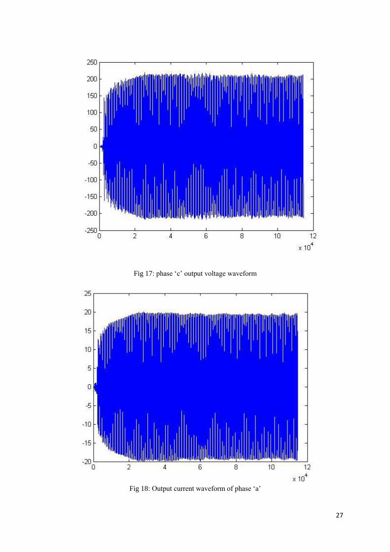
Fig 17: phase ‘c’ output voltage waveform
Fig 18: Output current waveform of phase ‘a’

28
Fig 19: Unfiltered voltage waveform of phase ‘a’.
Fig 20: IGBT/Diode current waveform

29
Conclusion:
Two simulations namely simulation 1 and simulation 2 have been done based on the
Simulink model presented above and the results of the waveforms for both the simulations
have been shown.
It was found that for Simulation1, the output current and voltage waveforms of the
inverter were of the desired sinusoidal nature with expected amplitude and frequency. For the
same simulation, the unfiltered voltage and IGBT/Diode current waveforms were of similar
nature.
On the other hand, for Simulation 2, even though the values of the filter inductance L and
filter conductance C were chosen from the stipulated range as calculated above according to
the accepted methodology given in Chapter III, the waveforms of the output current and
output voltage were not found to be of desired frequency and amplitude and there was
significant distortion from the expected sinusoidal nature.
It was also observed that, as the value of filter inductance L is decreased, within the
specified range, the amplitude of the distorted wave increases. Similarly, as the value of filter
capacitance C is increased, the level of distortion decreases.
So, the further scope of this project is to find out the reasons leading to these instabilities
within the particular range of filter parameters chosen according the accepted methodology.

30
References
1. N. Mohan, T.M. Undeland, W.P. Robbins, Power Electronics: Converters,
Applications, and Design (John Wiley and Sons, Singapore, 1995).
2. Muhammad H. Rashid, Power electronics: Circuits, Devices and Applications
(Pearson Education India, 01-Sep-2003).
3. Khaled H. Ahmed, Stephen J. Finney and Barry W. Williams (2007).’ Passive Filter
Design for Three-Phase Inverter Interfacing in Distributed Generation,’ Electrical
Power Quality and Utilisation, Journal Vol. XIII, No. 2, 2007.
4. Zoran Prof. Vukic, PhD Faculty of Electrical Engineering and Computing University
of Zagreb Ognjen Kuljaca Automation and Robotics Research Institute The
University of Texas at Arlington: LECTURES ON PID CONTROLLERS (April,
2002).