Embed Size (px)
Citation preview

END TERM EXAMINATION THIRD SEMESTER (BCA), DECEMBER – 2006
Time : Hours Maximum Marks : 75
Q. 1. (a) The following transfer statements specify a memory. Explain the memory operation in
each case. (5)
(i) RS M[AR]
(ii) M[AR] R3
(iii) R5 M[R5]
(b) Explain the difference between a direct and indirect address instruction. How may
references to memory are needed for each type of instruction to bring an operand into
a processor register? (5)
(c) Convert the following numerical arithmetic expressions into reverse polish notation and
show the stuck operations for evaluating the numerical result.
(3+4) [10(2+6) +8] (5)
(d) Explain Daisy-chain priority interrupt scheme. (5)
(e) Explain the concept of virtual memory. What are its advantages. (5)
UNIT – I
Q. 2. (a) Draw a diagram of a bus system using three-state buffers a decoder. (8.5)
(b) The 8-bit register AR, BR, CR and DR initiatory have the following values. (4)
AR = 11110010
BR = 11111111
CR = 10111001
DR = 11101010
Determine the 8-bit values in each register off the execution of the following sequence of
micro operations.
AR AR + BR
CR CR ^ DR, BR BR + 1
AR AR - CR
Paper Code : BCA – 203 Subject : Computer Architecture
Paper ID : 20203
Note : Q. 1 is compulsory. Attempt one question from each unit.
IITM HELPING HAND
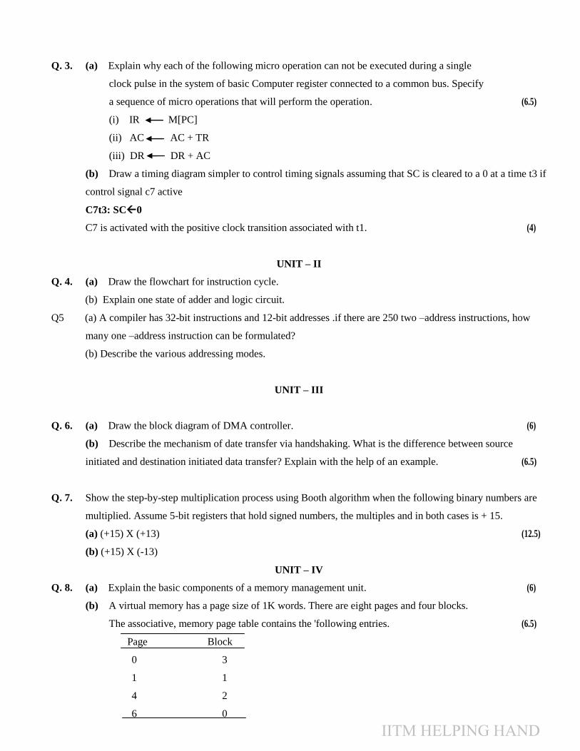
Q. 3. (a) Explain why each of the following micro operation can not be executed during a single
clock pulse in the system of basic Computer register connected to a common bus. Specify
a sequence of micro operations that will perform the operation. (6.5)
(i) IR M[PC]
(ii) AC AC + TR
(iii) DR DR + AC
(b) Draw a timing diagram simpler to control timing signals assuming that SC is cleared to a 0 at a time t3 if
control signal c7 active
C7t3: SC0
C7 is activated with the positive clock transition associated with t1. (4)
UNIT – II
Q. 4. (a) Draw the flowchart for instruction cycle.
(b) Explain one state of adder and logic circuit.
Q5 (a) A compiler has 32-bit instructions and 12-bit addresses .if there are 250 two –address instructions, how
many one –address instruction can be formulated?
(b) Describe the various addressing modes.
UNIT – III
Q. 6. (a) Draw the block diagram of DMA controller. (6)
(b) Describe the mechanism of date transfer via handshaking. What is the difference between source
initiated and destination initiated data transfer? Explain with the help of an example. (6.5)
Q. 7. Show the step-by-step multiplication process using Booth algorithm when the following binary numbers are
multiplied. Assume 5-bit registers that hold signed numbers, the multiples and in both cases is + 15.
(a) (+15) X (+13) (12.5)
(b) (+15) X (-13)
UNIT – IV
Q. 8. (a) Explain the basic components of a memory management unit. (6)
(b) A virtual memory has a page size of 1K words. There are eight pages and four blocks.
The associative, memory page table contains the 'following entries. (6.5)
Page Block
0 3
1 1
4 2
6 0
IITM HELPING HAND

Make a list of all virtual address (in decimal) that will cause a page fault if used by the CPU.
Q. 9. What do you mean by cache memory? Explain in detail mapping procedures used while considering
organization of cache memory. (12.5)
IITM HELPING HAND

END TERM EXAMINATION THIRD SEMESTER (BCA), DECEMBER – 2007
Time : 3 Hours Maximum Marks : 75
Q. 1. (a) What do you mean by register transfer language (RTL)? (3)
(b) What are shift registers? Where are these useful? (3)
(c) What is Instruction Cycle? What are its types? (4)
(d) What is associative rnemory? Outline its significance? (3)
(e) What is stack organization? (3)
(f) What are I/O interfaces? How are these important? (3)
(g) What kind of hardware is required for memory iT.2nagenenl? Discuss. (3)
(h) What is the relevance of priority interrupt? (3)
UNIT – I
Q. 2. What are micro-operations? What are its various types? Illustrate the implementation of each
category of micro-operations through its block diagram(s). (12.5)
Q. 3. (a) What is a bus? Design a bus system capable of transmitting data from any register from
a group or to registers (32-bits each) to any other register in a group of 8 registers
(32-bits each). Illustrate the logic through its block diagram?
(7.5)
(b) What is the importance of timing and control in the design of control unit? (5)
UNIT – II
Q. 4. (a) What do you understand by an Instruction Set? What are different types of instructions?
Discuss the significance of each type of instruction? (7)
(b) What are addressing modes? Discuss different types of addressing modes (5.5)
Q. 5. Explain the following :
(a) Instruction Format (6)
(b) ALU Design (6.5)
Paper Code : BCA – 203 (Batch-2005-2006 Subject : Computer Architecture
Paper ID : 20203
Note : Q. 1 is compulsory. Attempt One question from each unit.
IITM HELPING HAND

UNIT – III
Q. 6. Explain the following:
(a) Division algorithm (6)
(b) Direct Memory Access (DMA) (6.5)
Q. 7. (a) What is a floating Point number? What maximum and minimum floating point number can
be represented in a 64-bit computer having a sign bit for mantissa, 15 exponent bits and
32 mantissa bits? Also indicate the positive / negative and underflow ranges of the number
on the scale. (9)
(b) Differentiate between l synchronous and asynchronous data transfer? (3.5)
UNIT – IV
Q. 8. What is memory hierarch? Discuss each of elements in the hierarchy (12.5)
Q. 9. Differentiate between the following:
(a) RAM and ROM (6)
(b) Cache Memory and Virtual Memory (6.5)
IITM HELPING HAND

END TERM EXAMINATION THIRD SEMESTER (BCA), DECEMBER – 2008
Time : 3 Hours Maximum Marks : 75
Q1 (a) What is wrong with the following register transfer statements? (5)
(i) xT : AR(AR)c
, AR0 (ii) yT:R1 R2, R1R3
(b) What do you understand by the branch and save return address? (5)
(c) Explain the Indexed addressing mode. . (5)
(d) What is the difference between isolated I/O and memory mapped I/O? Also, explain the advantages and
disadvantages of each. (5)
(e) What is memory hierarchy in a computer system? (5)
UNIT-I
Q2 (a) Starting from an initial value of R=11011101, determine the sequence of binary values in R after a logical
shift-left, followed by a circular shift-right, followed by a logical Shift-right and a circular shift-left.
(4)
(b) Design an arithmetic circuit with one selection variable S and two n-bit date inputs A and B. The circuit
generates the following four arithmetic operations in conjunction will the input carry Cin. Draw the logic
diagram for the first two stages. (8)
Q3 (a) What is the difference between a direct and an indirect address instruction? How many references to
memory are needed for each type of instruction to bring an operand into a processor register?
(4.5)
(b) Draw the block diagram of control unit of basic computer and explain. (8)
UNIT-II
Q4 (a) Draw full adder and explain its logic circuit. (4.5)
(b) What are the various phases of an instruction cycle? Give the micro operations of
fetch and decode phases. How the first two register transfer statements are
implemented? (8)
S Cin=0 Cin=1 0 D=A+B D=A+1 1 D=A-1 D=A+B
c +1
Paper Code : BCA – 203 (Batch-2005-2006) Subject : Computer Architecture
Paper ID : 20203
Note : Q. 1 is compulsory. Attempt One question from each unit.
IITM HELPING HAND

Q5 (a) what is the reverse polish notation? Explain with an example. (4.5)
(b) Write down a program to evaluate Z = (A + B) *' (C -l- D) *' (G + H) by using three address instructions and
zero address instructions. (8)
UNIT-III
Q6 (a) What do you understand by the divide overflow? (4)
(b) Show the contents of registers E, A, Q and SC during the process of multiplication of two binary numbers,
11111(multiplicand) and 10101 (multiplier). The signs are not included. (8.5)
Q7 (a) Draw a block diagram for the DMA system showing the essential elements needed
for the DMA transfer in a computer system. (4.5)
(b) Explain the difference between the daisy chaining priority and parallel priority
interrupts. Draw the diagrams to explain their working. (8)
UNIT-IV
Q8 (a) Explain the concept of virtual memory. What are its advantages? (4.5)
(b) What is associative memory? Give and explain its architecture. (8)
Q9 (a) Explain the differences between cache and auxiliary memory. (4.5)
(b) A two way set associative cache memory uses blocks of four words. The cache
can accommodate a total of 2048 words from main memory. The main memory size is
128K x 32. (8) (i) Formulate all pertinent information required to construct the cache memory.
(ii) What is the size of the cache memory?
*********
IITM HELPING HAND

END TERM EXAMINATION THIRD SEMESTER (BCA), DECEMBER – 2009
Time: 3 Hours Maximum marks:75
Q1 Attempt any ten from the following:- (10x2.5=25)
(a)Draw the block diagram for the hardware that implements the following statement:
x+yz: ARAR+BR, where AR and BR are two n-bit registers and x, y and z are control variables.
(b) Design a 4-bit combinational circuit decrementer using four full adders.
(c) What are the two instruction needed in the basic computer in order to set the E flip flop to 1?
(d)A computer uses a memory unit with 256 K words of 32 bits each. A binary instruction code is
stored in one word of memory. The instruction has four parts: an indirect bit, an operation code,
a register code part to specify one of 64 registers and an address part .Draw the instruction word
format and indicate the number of bits in each part.
(e)Write any three function of stack.
(f) Why does DMA have priority over CPU when both request a memory transfer?
(g) Define overflow .How can we detect overflow?
(h)Give two advantages of booth multiplication.
(i) List various registers with their function required for basic computer function.
(j) (i)How many 128x8 RAM chips are needed to provide a memory capacity of 2048 bytes?
(ii) How many lines of address bus must be used to access 2048 bytes of memory?
(k) A ROM chip of 1024x8 bits has four select inputs and operates from a 5-volt power supply .How
many pins are needed for the IC package ? Draw a block diagram and label all input and output
terminals in the ROM.
(l) Define hit ratio.
Paper Code: BCA – 203 Subject: computer Architecture
Paper ID: 20203
Note: Q. 1 is compulsory. Attempt one question from each unit.
IITM HELPING HAND

UNIT –I
Q2 (a) Tabulate various shift micro operation and design a 4 bit combination circuit shifter. (5)
(b) the output of four registers R0,R1,R2,R3 are connected through 4-to 1 line multiplexers to the
inputs of a fifth register ,R5 .Each register is eightr bits longs .the required transfers are dictated
by four timing variables T0 through T3 as follows:
To: R5R0
T1 : R5R1
T2: R5R2
T3 : R5R3
Timing variables are mutually exclusive .Draw a block diagram showing the hardware implementation of
the register transfers. (5)
(c) Starting from an initial value of R=11011101, determine the sequence of binary values
in R after a logical shift-left followed by a shift –right and a circular shift –left. (2.5)
Q3 (a) Describe the hardware implementation of logic micro operation .draw the diagram of one stage of
logic circuit used with AND,OR,NAND and XOR gates. (5)
(b)What is the difference between a direct and indirect address instruction? (5)
(c)Give a suitable example to discuss insert operation. (2.5)
UNIT-II
Q4 (a)Design a flow chart showing instruction cycle and interrupt cycle for basic computer operation.
(5)
(b)Tabulate various memory reference instruction .explain BUN and BSA (5)
(c) Giving suitable block diagram show major components of CPU. (2.5)
Q5 (a) illustrate the influence of number of address on X=(R+S)(U+V) using three address,two address
and zero address instruction. (5)
(b)What is stack organization ? Describe its function using a suitable example .Define stack limit.
(5)
(c)What is the difference between implied and immediate addressing modes? (2.5)
IITM HELPING HAND

UNIT-III
Q6 (a) Design and discuss 2 bit by 3 bit array multiplier .give its major advantages. (5)
(b) Taking multiplicand 11111 and multiplier 01001 designs a table of multiplication with booth
multiplication algorithm. (5)
(C) Give registers configuration for hardware implementation of signed 2’s compliment
addition/subtraction. (2.5)
Q7 (a) What do you understand by hand shaking? Discuss using suitable diagram.
(i) Source initiated transfer using hand shaking.
(ii)Destination initiated transfer using hand shaking. (5)
(b)What is priority? Name various types of priority .Discuss Daisy chaining priority in
brief. (5)
(c)list four peripherals devices that produce an acceptable output for a person to understand
(2.5)
UNIT –IV
Q8 (a) What is mapping? Name various types of mapping .Discuss direct mapping in brief. (5)
(b) Write a short note on memory hierarchy. (5)
(c)A computer uses RAM chips of 1024x1 capacity. (2.5)
(i)How many chips are needed to provide a memory capacity of 1024 bytes?
(ii) How many chips are needed to provide a memory capacity of 16K bytes?
Q9 (a) Giving suitable block diagram differentiates between RAM and ROM (5)
(b)Write a short note on auxiliary memory (5)
(C)Draw a block diagram of associative memory. (2.5)
IITM HELPING HAND

END TERM EXAMINATION THIRD SEMESTER (BCA), DECEMBER – 2010
Time : Hours Maximum Marks : 75
Q. 1. (a) Design a 4-bit combinational circuit decrementer using four full- adder circuits. (5)
(b) Explain interrupt cycle with an example. (5)
(c) What is an Input-Output interface? Why is it needed? (5)
(d) Explain the concept of virtual memory. How is it implemented? (5)
(e) What is associative memory? Explain its architecture. (5)
UNIT – I
Q. 2. (a) Describe Basic Instruction Set. Is it complete? Justify. (8.5)
(b) Register A holds the 8-bit binary 11011001. Determine the B operand and
the logic micro operation to be performed in order to change the value in A to : (4)
(i) 01101101
(ii) 11111101
Q. 3. (a) Draw a diagram of bus system for four registers with 8-bit each using three-state buffers
and decoder. (6.5)
(b) Explain hard wired control unit organization. (6)
UNIT – II
Q. 4. (a) Show the contents in hexadecimal of registers PC, AR, DR, IR and SC of the basic
computer when an ISZ indirect instruction is fetched from memory and executed.
The initial content of PC is 7FF. The content of memory at address 7FF is EA 9F.
The content of memory at address A9F is OC35. The content of memory at address
C35 is FFFF. (5)
(b) Convert the following arithmetic expressions from infix to reverse Polish notation :
A + B * [C * D + E * ( F + G)] (4.5)
(c) Give three examples each of external and internal interrupts. (3)
\
Paper Code : BCA – 203 Subject : Computer Architecture
Paper ID : 20203
Note : Q. 1 is compulsory. Attempt One question from each unit.
IITM HELPING HAND
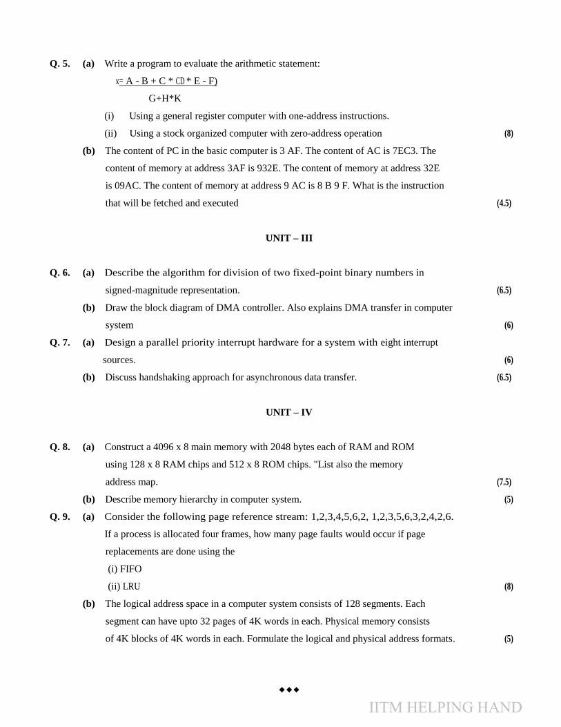
Q. 5. (a) Write a program to evaluate the arithmetic statement:
x= A - B + C * CD * E - F)
G+H*K
(i) Using a general register computer with one-address instructions.
(ii) Using a stock organized computer with zero-address operation (8)
(b) The content of PC in the basic computer is 3 AF. The content of AC is 7EC3. The
content of memory at address 3AF is 932E. The content of memory at address 32E
is 09AC. The content of memory at address 9 AC is 8 B 9 F. What is the instruction
that will be fetched and executed (4.5)
UNIT – III
Q. 6. (a) Describe the algorithm for division of two fixed-point binary numbers in
signed-magnitude representation. (6.5)
(b) Draw the block diagram of DMA controller. Also explains DMA transfer in computer
system (6)
Q. 7. (a) Design a parallel priority interrupt hardware for a system with eight interrupt
sources. (6)
(b) Discuss handshaking approach for asynchronous data transfer. (6.5)
UNIT – IV
Q. 8. (a) Construct a 4096 x 8 main memory with 2048 bytes each of RAM and ROM
using 128 x 8 RAM chips and 512 x 8 ROM chips. "List also the memory
address map. (7.5)
(b) Describe memory hierarchy in computer system. (5)
Q. 9. (a) Consider the following page reference stream: 1,2,3,4,5,6,2, 1,2,3,5,6,3,2,4,2,6.
If a process is allocated four frames, how many page faults would occur if page
replacements are done using the
(i) FIFO
(ii) LRU (8)
(b) The logical address space in a computer system consists of 128 segments. Each
segment can have upto 32 pages of 4K words in each. Physical memory consists
of 4K blocks of 4K words in each. Formulate the logical and physical address formats. (5)
IITM HELPING HAND

END TERM EXAMINATION THIRD SEMESTER (BCA), DECEMBER – 2011
Time : 3 Hours Maximum Marks : 75
Q1. (a) Draw a diagram of a bus system for four register with 8-bit each using three - state buffers and a
decoder instead of the multiplexers. (5)
(b) Give symbolic description for following Memory-Reference instructions –
(i) AND (ii) BSA (iii) STA (iv) LDA (v) BUN (5)
(c) Design a one stage of the daisy – chain priority arrangement. (5)
(d) Draw a block diagram of associative memory. What is match logic? (5)
(e) Explain the concept of cache memory. How it is implemented? (5)
UNIT – I
Q2. (a) A digital computer has a common bus system for 16 registers of 32 bit each. The bus is constructed with
MUXs. (6)
(i). How many MUX are there in the bus?
(ii). What size of MUXs is needed?
(iii). How many selection inputs are there in each MUX?
(b) Design a one stage logic design that performs the four operations of X-OR, AND, OR and Complement.
Use two selection variables. (6.5)
Q3 (a) What is the difference between a direct and an indirect address instruction? How many references to
Memory are needed for each type of instruction to bring an operand into a processor register? (6)
(b) Draw a block diagram of the control unit of basic computer. What is the purpose of IR & SC in it? (6.5)
UNIT – II
Q4 (a) Explain how interrupt cycle is a hardware implementation of a BSA operation. Draw the flow chart of
interrupt cycle. (8)
(b) List some Register - reference Instructions. (4.5)
Q5 (a) Draw a general bus organization for 7CPU using 2 MUX, 1 ALU and 1 Decoder. (6)
(b) Write down the sequence of micro operations involved in PUSH and POP operations for a stack. Show
The stack operation to evaluate. (6.5)
UNIT – III
Q6 (a) Explain Booth’s algorithm for multiplication of signed 2’s complement numbers. (6.5)
(b) Explain DMA controller with the help of block diagram. (6)
Q7 (a) What is source – initiated transfer using handshaking? Explain with block diagram, timing diagram and
sequence of events. (6.5)
(b) What is programmed I/O and Interrupt – Initiated I/O? (6)
Paper Code : BCA203 Subject : Computer Architecture
Note : Attempt One question from each unit including Q.no. 1 which is compulsory.
IITM HELPING HAND

UNIT – IV
Q8 (a) How many 128x8 RAM chips are needed to provide a memory capacity of 2048 bytes? (2)
(b) Explain the basic components of memory management unit. (4)
(c) What is write-through and write back method? (3)
(d) If a computer uses RAM chips of 1024x1 capacity, how many chips are needed and how should their
address lines be connected to provide a memory capacity of 1024 bytes? (3.5)
Q9 (a) An address space is specified by 24 bits and the corresponding memory space by 16 bits. (6)
(i). How many words are there in the address space?
(ii). How many words are there in the memory space?
(iii). If a page consists of 2K words, how many pages and blocks are there in the system?
(b) How average time is calculated to read one sector in a magnetic disk system? (3)
(c) What is bootstrap loader and locality of reference? (3.5)
************
IITM HELPING HAND

IITM HELPING HAND