Embed Size (px)
Citation preview
Endurance and Scaling Trends of Novel Access-Devices for Multi-Layer Crosspoint-Memorybased on Mixed-Ionic-Electronic-Conduction (MIEC) Materials
R. S. Shenoy, K. Gopalakrishnan, B. Jackson, K. Virwani, G. W. Burr, C. T. Rettner,A. Padilla, D. S. Bethune, R. M. Shelby, A. J. Kellock, M. Breitwisch†, E. A. Joseph†, R. Dasaka†,
R. S. King, K. Nguyen, A. N. Bowers, M. Jurich, A. M. Friz, T. Topuria, P. M. Rice, and B. N. KurdiIBM Almaden Research Center, 650 Harry Road, San Jose, CA 95120 (†IBM T. J. Watson Research Center, Yorktown Heights, NY 10598)
Tel: (408) 927{–2362, –3721}, Fax: (408) 927–2100, E-mail: {rsshenoy, kailash}@us.ibm.com
AbstractWe demonstrate compact integrated arrays of BEOL-friendly
novel access devices (AD) based on Cu-containing MIEC materi-als[1-3]. In addition to the high current densities and large ON/OFFratios needed for Phase Change Memory (PCM), scaled-down ADsalso exhibit larger voltage margin Vm, ultra-low leakage (<10pA),and much higher endurance (>108) at high current densities. UsingCMP, all–good 5×10 AD arrays with Vm > 1.1V are demonstratedin a simplified CMOS-compatible diode-in-via (DIV) process.Keywords: Access device, MIEC, PCM, NVM, MRAM, RRAM
IntroductionFor PCM or any other nonvolatile memory (NVM) to be as
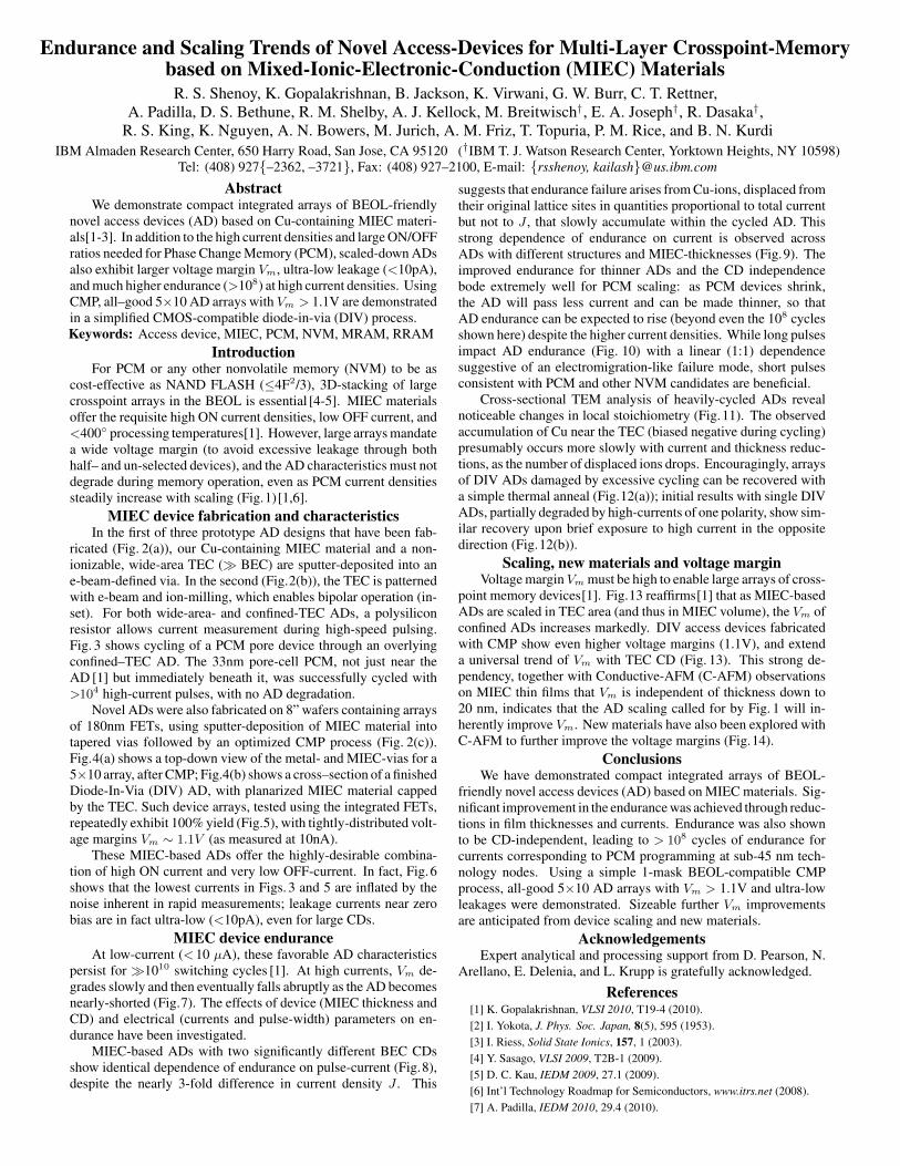
cost-effective as NAND FLASH (≤4F2/3), 3D-stacking of largecrosspoint arrays in the BEOL is essential [4-5]. MIEC materialsoffer the requisite high ON current densities, low OFF current, and<400◦ processing temperatures[1]. However, large arrays mandatea wide voltage margin (to avoid excessive leakage through bothhalf– and un-selected devices), and the AD characteristics must notdegrade during memory operation, even as PCM current densitiessteadily increase with scaling (Fig.1)[1,6].
MIEC device fabrication and characteristicsIn the first of three prototype AD designs that have been fab-
ricated (Fig. 2(a)), our Cu-containing MIEC material and a non-ionizable, wide-area TEC (� BEC) are sputter-deposited into ane-beam-defined via. In the second (Fig.2(b)), the TEC is patternedwith e-beam and ion-milling, which enables bipolar operation (in-set). For both wide-area- and confined-TEC ADs, a polysiliconresistor allows current measurement during high-speed pulsing.Fig. 3 shows cycling of a PCM pore device through an overlyingconfined–TEC AD. The 33nm pore-cell PCM, not just near theAD [1] but immediately beneath it, was successfully cycled with>104 high-current pulses, with no AD degradation.
Novel ADs were also fabricated on 8” wafers containing arraysof 180nm FETs, using sputter-deposition of MIEC material intotapered vias followed by an optimized CMP process (Fig. 2(c)).Fig.4(a) shows a top-down view of the metal- and MIEC-vias for a5×10 array, after CMP; Fig.4(b) shows a cross–section of a finishedDiode-In-Via (DIV) AD, with planarized MIEC material cappedby the TEC. Such device arrays, tested using the integrated FETs,repeatedly exhibit 100% yield (Fig.5), with tightly-distributed volt-age margins Vm ∼ 1.1V (as measured at 10nA).
These MIEC-based ADs offer the highly-desirable combina-tion of high ON current and very low OFF-current. In fact, Fig.6shows that the lowest currents in Figs. 3 and 5 are inflated by thenoise inherent in rapid measurements; leakage currents near zerobias are in fact ultra-low (<10pA), even for large CDs.
MIEC device enduranceAt low-current (<10 µA), these favorable AD characteristics
persist for �1010 switching cycles [1]. At high currents, Vm de-grades slowly and then eventually falls abruptly as the AD becomesnearly-shorted (Fig.7). The effects of device (MIEC thickness andCD) and electrical (currents and pulse-width) parameters on en-durance have been investigated.
MIEC-based ADs with two significantly different BEC CDsshow identical dependence of endurance on pulse-current (Fig.8),despite the nearly 3-fold difference in current density J . This
suggests that endurance failure arises from Cu-ions, displaced fromtheir original lattice sites in quantities proportional to total currentbut not to J , that slowly accumulate within the cycled AD. Thisstrong dependence of endurance on current is observed acrossADs with different structures and MIEC-thicknesses (Fig.9). Theimproved endurance for thinner ADs and the CD independencebode extremely well for PCM scaling: as PCM devices shrink,the AD will pass less current and can be made thinner, so thatAD endurance can be expected to rise (beyond even the 108 cyclesshown here) despite the higher current densities. While long pulsesimpact AD endurance (Fig. 10) with a linear (1:1) dependencesuggestive of an electromigration-like failure mode, short pulsesconsistent with PCM and other NVM candidates are beneficial.
Cross-sectional TEM analysis of heavily-cycled ADs revealnoticeable changes in local stoichiometry (Fig.11). The observedaccumulation of Cu near the TEC (biased negative during cycling)presumably occurs more slowly with current and thickness reduc-tions, as the number of displaced ions drops. Encouragingly, arraysof DIV ADs damaged by excessive cycling can be recovered witha simple thermal anneal (Fig.12(a)); initial results with single DIVADs, partially degraded by high-currents of one polarity, show sim-ilar recovery upon brief exposure to high current in the oppositedirection (Fig.12(b)).
Scaling, new materials and voltage marginVoltage margin Vm must be high to enable large arrays of cross-
point memory devices[1]. Fig.13 reaffirms[1] that as MIEC-basedADs are scaled in TEC area (and thus in MIEC volume), the Vm ofconfined ADs increases markedly. DIV access devices fabricatedwith CMP show even higher voltage margins (1.1V), and extenda universal trend of Vm with TEC CD (Fig. 13). This strong de-pendency, together with Conductive-AFM (C-AFM) observationson MIEC thin films that Vm is independent of thickness down to20 nm, indicates that the AD scaling called for by Fig. 1 will in-herently improve Vm. New materials have also been explored withC-AFM to further improve the voltage margins (Fig.14).
ConclusionsWe have demonstrated compact integrated arrays of BEOL-
friendly novel access devices (AD) based on MIEC materials. Sig-nificant improvement in the endurance was achieved through reduc-tions in film thicknesses and currents. Endurance was also shownto be CD-independent, leading to > 108 cycles of endurance forcurrents corresponding to PCM programming at sub-45 nm tech-nology nodes. Using a simple 1-mask BEOL-compatible CMPprocess, all-good 5×10 AD arrays with Vm > 1.1V and ultra-lowleakages were demonstrated. Sizeable further Vm improvementsare anticipated from device scaling and new materials.
AcknowledgementsExpert analytical and processing support from D. Pearson, N.
Arellano, E. Delenia, and L. Krupp is gratefully acknowledged.
References[1] K. Gopalakrishnan, VLSI 2010, T19-4 (2010).[2] I. Yokota, J. Phys. Soc. Japan, 8(5), 595 (1953).[3] I. Riess, Solid State Ionics, 157, 1 (2003).[4] Y. Sasago, VLSI 2009, T2B-1 (2009).[5] D. C. Kau, IEDM 2009, 27.1 (2009).[6] Int’l Technology Roadmap for Semiconductors, www.itrs.net (2008).[7] A. Padilla, IEDM 2010, 29.4 (2010).
PCM CD:
65 45 32 22 16 810uA
20uA
40uA
100uA
200uA
400uA
Technology node F [nm]
IBM PCM pore devices
581014202841
PCM
RES
ET c
urre
nt
w/ aggressivePCM scaling(PCM CD = 0.5F)
ITRS
65 45 32 22 16 12 8
5
10
20
Technology node F [nm]
AD current density [MA/cm2]
aggressive
[nm]
12
ITRS roadmap
Fig. 1 PCM requires large Access Device (AD) current den-sities, yet absolute RESET current will decrease with scaling.
MIEC
TEC
ILDBEC
poly-Si
MIECTEC
ILDBEC
poly-Si
a)
b) via
ILD
TECM1
via
BECvia
MIEC
FET
c)
Fig. 2 MIEC-based ADs with non-ionizable electrodes are fabricated on 4” wafers with a) wide-area TECs (� BEC), b) TECs patterned to enable bipolar operation (inset) with ion-milling,and c) on 8” wafers with integrated FETs using Chemical-Mechanical Polishing (CMP).
-1 -0.8 -0.6 -0.4 -0.2 0 0.2 0.4 0.6 0.8 110pA
100pA
1nA
10nA
100nA
1uA
voltage [V]
RESET
SET >10x
MIEC
GST
poly-Si
PCM TEC = AD BEC
TiN
PCM
AD
33 nm
80 nm
AD TEC 200 nm
TEC
100 1k 10k10pA100pA
1nA10nA
100nA1uA
10uA100uA
1mA
Current
PulsesRESET
SET
Current
Fig. 3 Cycling of a 33nm pore-cell PCM, with SET,RESET, and read performed through an overlying AD(80nm BEC), which showed no degradation despite the> 104 high-current pulses. The 200nm TEC allowed“good polarity” (positive-on-TEC) PCM operation[7].
a)
BEC
TEC
MIEC180nm
80nm
b)
Fig. 4 a) Top-down view of metal- andMIEC-vias for a 5×10 array (w/ dummyrows/columns), after CMP; (b) TEM cross–section of a Diode-In-Via (DIV) AD, with pla-narized MIEC material capped by the TEC.
80 nm BEC / 180 nm TEC
TEC voltage [V]-0.6 -0.4 -0.2 0 0.2 0.4 0.6
100pA
1nA
100nA
10nA
1uA
Num
ber o
f dev
ices
TEC voltage for 10nA leakage
50
40
25
10
0-1.0 -0.5 0 0.5 1.0
Vm = 1.1VCurrent
Fig. 5 Measured i-v characteristics for a 5×10 array ofDIV ADs, tested with integrated FETs, showing largevoltage margin (Vm ∼ 1.1V) and tight distributions.
100fA
1pA
10pA
100pA
1nA
10nA
100nA
Cur
rent
[per
dev
ice]
-0.5 -0.4 -0.3 -0.2 -0.1 0 0.1 0.2 0.3 0.4 0.5
Voltage [V]
Single device20 devices25 devices45 devices
Slow measurements(20x 16ms integration)
(Average of 20 measurements at 160sec integration)
Single device, rapid
Diode-in-Via (TEC: 180nm, BEC: 80nm)
Fig. 6 Slow measurements, performed on singleor multiple all–good devices, reveal that leakagecurrents in MIEC-based ADs near 0V are<10pA.
-0.4 -0.3 -0.2 -0.1 0TEC voltage [V]
Cur
rent
Current pulse
leakage
Wide-area TEC, 80nm BEC
100pA
10nA
1uA
100uA
(left half of Vm )
Vb
10k 100k 1e6 1e7 1e91e8
-0.2V
0V
failure criteria: 100mV shift (16% Vm )-0.4V
100pA
10nA100nA
1uA
1nA
Pulses Pulses
-0.4-0.6 0 0.4 0.6voltageC
urre
nt
Current pulse
leakage
DIV: 185nm TEC, 95nm BEC
10nA
1uA
100uA
0.6V
0V
1.0V
100pA
10nA100nA
1uA
1nA TEC
0.2-0.2
failure criteria: 200mV shift (18% Vm )0.8V0.4V0.2V
100 1k 10k 1e71e6Va
Vm100pA
-Vb 100k
Fig. 7 Both a) wide-area TEC and b) DIV MIEC-based ADscan operate without degradation for many high-current pulses, buteventually a change from low- to high-leakage occurs. This changeis abrupt in all but the thickest ADs.
100 200 300 4001e3
1e4
1e5
1e6
1e7
Current [uA]
Endurance47nm BEC80nm BEC
(wide-area TECs)
Fig. 8 MIEC-based AD endurancedepends on current, but is indepen-dent of BEC CD, despite the nearly3-fold change in current density.
50 100 150 200 250 300 350 40010
100
1e3
1e4
1e5
1e6
1e7
1e8
1e9
Current [uA]
Endu
ranc
e
6545403222 (PCM RESET current)F
DIV ADs, cycled positive on TEC
50nm in 40nm ILD70nm in 20nm ILD70nm in 40nm ILD
40nm in 40nm ILDMIEC thickness:
80nm BEC ADs, cyclednegative on Wide-area TEC
185nm TEC, 95nm BEC, 115nm thick MIEC
180nm TEC, 80nm BEC, 145nm thick MIEC
nominal
Fig. 9 ADs show better endurance as the thickness,and thus the volume from which Cu+ is accumulatedduring cycling (see Fig.11) , becomes smaller.
100ns 1us 10us 100us 1ms
1e4
1e5
1e6
Pulse Duration95nm BECDIV AD, cycled positive on 185nm TEC
Wide-area TEC ADs with 70nm-thick MIEC in 40nm ILD,
cycled negative on TEC40nm BEC80nm BEC, < 200uA80nm BEC, > 300uA
Endurance
Fig. 10 For both wide-area TEC and DIV ADs,endurance improves as pulse duration is reduced.
nominal Cu-richCu-poor
a) b)
Fig. 11 Local stoichiometry from TEM/EELS of wide-area TEC, 80nm BEC ADs a) as-fabricated, and b) after425,000 cycles at 325µA. Regions near the TEC (biasednegative for cycling) have become markedly Cu-rich.
100nA
100pA
After repeatedhigh-current,
negative-on-TECpulses
1uA
10nA
1nA
Current
TECvoltage
-0.5V 0V 0.5VTEC voltage for 10nA leakage [V]
0.2 0.4 0.6-0.6 -0.4 -0.2 00
10
20
30
40
50
Num
ber o
f dev
ices
Initial
degraded by cycling
recoveredby anneal
a)b)
Fig. 12 Low-leakage i-v characteristics that have been de-graded by endurance failure or high-current pulses can berecovered by either a) thermal annealing, or b) high-currentpulses of the opposite polarity. This implies that local accumu-lations of Cu shown in Fig.11 can be successfully redistributed.
80nmBEC
100nm 1um 10um0.5
0.6
0.7
0.8
0.9
1
1.1
1.2
TEC CD
Vm [V]
40nm BEC
Fig. 13 Wide-area-TEC, confined-TEC, andDIV ADs exhibit a common trend: Vm in-creases sharply as TEC CD is scaled down.
[a.u.]
Tip bias [a.u.]
Current
Material BMaterial C
PORMIECmaterial
Fig. 14 Conductive-AFM measurements (small-areatip on various MIEC materials on unpatterned BEC)provide early guidance on the Vm (but not on leakagecurrent) to be expected from wide-area TEC ADs.