Embed Size (px)
Citation preview

ENERGY, AREA AND SPEED OPTIMIZED SIGNAL PROCESSING ON FPGA
A THESIS SUBMITTED IN PARTIAL FULFILLMENT
OF THE REQUIREMENTS FOR THE DEGREE OF
Master of Technology In
VLSI design and embedded system
By
DURGA DIGDARSINI
Department of Electronics and Communication Engineering
National Institute of Technology, Rourkela Rourkela-769008
2007

ENERGY, AREA AND SPEED OPTIMIZED SIGNAL PROCESSING ON FPGA
A THESIS SUBMITTED IN PARTIAL FULFILMENT
OF THE REQUIREMENTS FOR THE DEGREE OF
Master of Technology
In Electronics and Communication Engineering
By
DURGA DIGDARSINI
Under the Guidance of
Prof. KAMALAKANTA MAHAPATRA
Department of Electronics and Communication Engineering National institute of Technology
Rourkela-769008 2007

National Institute of Technology
Rourkela
CERTIFICATE
This is to certify that the thesis entitled, “Energy, Area and speed Optimized Signal
Processing On FPGA” submitted by Ms.Durga Digdarsini in partial fulfillment of the
requirements for the award of Master of Technology Degree in the Department of Electronics
and Communication Engineering, with specialization in “VLSI design and embedded system”
at the National Institute of Technology, Rourkela (Deemed University) is an authentic work
carried out by her under my supervision and guidance.
To the best of my knowledge, the matter embodied in the thesis has not been submitted to any
other University / Institute for the award of any Degree or Diploma.
Date: Prof. K. K. Mahapatra
Department of Electronics and Communication engineering
National Institute of Technology, Rourkela
Pin - 769008

i
National Institute of Technology Rourkela
ACKNOWLEDGEMENTS
I am thankful to Dr. K. K. Mahapatra, Professor in the department of Electronics and
Communication Engineering, NIT Rourkela for giving me the opportunity to work under him
and lending every support at every stage of this project work. I truly appreciate and value him
esteemed guidance and encouragement from the beginning to the end of this thesis. I am
indebted to his for having helped me shape the problem and providing insights towards the
solution.
I express my gratitude to Dr.G.P.Panda, Professor and Head of the Department,
Electronics and Communication Engineering for his invaluable suggestions and constant
encouragement all through the thesis work.
I would also like to convey my sincerest gratitude and indebt ness to all other faculty
members and staff of Department of Electronics and Communications Engineering, NIT
Rourkela, who bestowed their great effort and guidance at appropriate times without which it
would have been very difficult on my part to finish the project work. I also very thankful to all
my class mates and friends of VLSI lab-I especially sushant, Jitendra Das (Phd scholar),
srikrishna who always encouraged me in the successful completion of my thesis work.
Date
Durga Digdarsini
Dept. of Electronics & Communications Engineering
National Institute of Technology, Rourkela
Pin - 769008

ii
TABLE OF CONTENTS
A. Acknowledgement i
B. Contents ii
C. Abstract v
D. List of Figures vi
E. List of Tables viii
F. List of Acronyms ix
G. Chapters
1. Introduction
1.1 Introduction 1
1.2 Motivations 1
1.3 Literature review 2
1.4 Organization 4
1.5 Summary 4
2. Energy Efficient Modeling Technique
2.1 Introduction 5
2.2 Domain Specific Modeling 5
2.2.1 High level energy model 7
2.2.2 Generation of power function 9
2.2.2 Power function builder curve fitting 12
3. Matrix Multiplication
3.1 Systolic array 13
3.1.1 Systolic operation 13
3.2 Matrix multiplication algorithm 15
3.2.1 Matrix- matrix multiplication on systolic array 16
4. Energy Efficient Matrix Multiplication
4.1 Introduction 18
4.2 Methodology 18
4.3 Algorithms and architectures in the design 19
4.3.1 Theorems 19

iii
4.3.2 Timing diagrams and explanations 20
4.4 Word width decomposition technique 24
4.4.1 Architectures with word width decomposition 25
4.5 Construction of High level energy model 29
4.5.1 Generation of energy, area and latency functions 30
4.6 Results and discussion 33
4.6.1 Functions generation from curve fitting 33
4.6.2 Comparison of design at high level 35
4.6.3 Estimation of error at low level 36
4.6.4 Conclusion 36
5. Fast Fourier Transform
5.1 Introduction 37
5.2 Discrete Fourier Transform 37
5.3 Fast Fourier Transform 38
5.3.1 Cooley Tukey algorithm 39
5.3.2 Radix 2 FFT algorithm 40
5.3.3 Radix 4 FFT algorithm 43
6. Energy Efficient Fast Fourier Transform
6.1 Introduction 47
6.2 Methodology 47
6.2.1 Sources of energy dissipation 48
6.2.2 Techniques of energy reduction 48
6.3 Algorithm and architectures for Fast Fourier Transform 51
6.3.1 Components used in architecture 52
6.4 Complex multiplier in the design 55
6.4.1 Various multiplier architectures 55
6.5 Distributed arithmetic 60
6.5.1 Derivation of DA algorithm 60
6.5.2 FFT with distributed arithmetic 64
6.6 Construction of High level energy model 64
6.6.1 Generation of energy, area and latency functions 65
6.7 Results and discussion 66

iv
6.7.1 Comparison of design at high level 67
6.7.2 Estimation of error at low level 67
6.7.3 Conclusions 67
7. Conclusions
7.1 Conclusion 68
7.2 Further work 68
H. References 70

v
ABSTRACT
Matrix multiplication and Fast Fourier transform are two computational intensive DSP
functions widely used as kernel operations in the applications such as graphics, imaging and
wireless communication. Traditionally the performance metrics for signal processing has been
latency and throughput. Energy efficiency has become increasingly important with proliferation
of portable mobile devices as in software defined radio.
A FPGA based system is a viable solution for requirement of adaptability and high
computational power. But one limitation in FPGA is the limitation of resources. So there is need
for optimization between energy, area and latency. There are numerous ways to map an
algorithm to FPGA. So for the process of optimization the parameters must be determined by
low level simulation of each of the designs possible which gives rise to vast time consumption.
So there is need for a high level energy model in which parameters can be determined at
algorithm and architectural level rather than low level simulation.
In this dissertation matrix multiplication algorithms are implemented with pipelining and
parallel processing features to increase throughput and reduce latency there by reduce the energy
dissipation. But it increases area by the increased numbers of processing elements. The major
area of the design is used by multiplier which further increases with increase in input word width
which is difficult for VLSI implementation. So a word width decomposition technique is used
with these algorithms to keep the size of multipliers fixed irrespective of the width of input data.
FFT algorithms are implemented with pipelining to increase throughput. To reduce
energy and area due to the complex multipliers used in the design for multiplication with twiddle
factors, distributed arithmetic is used to provide multiplier less architecture. To compensate
speed performance parallel distributed arithmetic models are used.
This dissertation also proposes method of optimization of the parameters at high level for
these two kernel applications by constructing a high level energy model using specified
algorithms and architectures. Results obtained from the model are compared with those obtained
from low level simulation for estimation of error.

vi
LIST OF FIGURES
Figure 2.1 System wide energy function generation 6
Figure 2.2 Domain specific modeling 8
Figure 2.3 MILAN Frame work 10
Figure 2.4 Functions generation by low level simulation 11
Figure 3.1 Functional units of systolic array 14
Figure 3.2 Pipelined 1D systolic array 14
Figure 3.3 2D systolic square array 14
Figure 3.4 2D systolic triangular array 14
Figure 3.5 Firing of cells in systolic array 16
Figure 3.6 Matrix multiplication on a 2D systolic array 17
Figure 4.1 Matrix multiplication on a linear systolic array 19
Figure 4.2 Architecture of processing element for theorem 1 20
Figure 4.3 Timing diagram for theorem 1 21
Figure 4.4 Architecture of processing element for theorem 2 23
Figure 4.5 Decomposition unit 25
Figure 4.6 Mechanism to support 2’s complement data 27
Figure 4.7 Composition unit 28
Figure 4.8 Theorem 1 with word width decomposition 29
Figure 4.9 Generation of energy and area functions 31
Figure 4.10 Best fit curves from curve fitting for generation of functions 33

vii
Figure 5.1 Flow graph of 8 point FFT calculated using two N/2 point DFT 42
Figure 5.2 Flow graph of 8 point radix 2 DIT FFT 43
Figure 5.3 Flow graph of 8 point radix 2 DIF FFT 44
Figure 5.4 Flow graph of 16 point radix 4 DIT FFT 44
Figure 5.5 Radix 4 FFT butterfly unit 46
Figure 6.1 FFT architecture with Hp = 2 and VP = 1 51
Figure 6.2 FFT architecture with Hp = 2 and VP = 4 52
Figure 6.3 Radix 4 butterfly 54
Figure 6.4 Data storing by data buffers 54
Figure 6.5 Data buffer 54
Figure 6.6 Complex multiplier 54
Figure 6.7 Array multiplier 56
Figure 6.8 DALUT contents and addressing 62
Figure 6.9 Fully parallel DA model 63
Figure 6.10 Modified architecture with distributed arithmetic 64

viii
List of Tables
Table 4.1 Functions for theorem 1 and theorem 2 32
Table 4.2 Functions for theorems with word width decomposition 32
Table 4.3 Results for theorem 1 with word width decomposition 35
Table 4.4 Results for theorem 2 with word width decomposition 35
Table 4.5 Comparisons of results 36
Table 6.1 Example of multiplication using Booth’s algorithm 58
Table 6.2 Modified Booth recoding table 59
Table 6.3 DALUT contents 62
Table 6.4 Comparison of results obtained from functions 67
Table 6.5 Comparison of results with actual values and error estimation 67

ix
LIST OF ACRONYMS
SDR Software defined radio
FPGA Field programmable gate array
LUT Look up table
MILAN Model based Integrated Simulation Framework
RModule Relocatable module
ISE Integrated student edition
MUX Multiplexer
MAC Multiplier and accumulator
PE Processing element
RAM Read and write memory
SRAM Slice based RAM
BRAM Block RAM
DFT Discrete Fourier Transform
FFT Fast Fourier Transform
DA Distributed arithmetic
DALUT Distributed arithmetic look up table
DIT Decimation in time
DIF Decimation in frequency
DBUF Data buffer

Chapter 1
INTRODUCTION

1
1.1 Introduction
Matrix multiplication and Fast Fourier Transform are important tools used in the
Digital Signal Processing applications. Each of them is compute-intensive portion of
broadband beam forming applications such as those generally used in software defined radio
and sensor networks. These are frequently used kernel operations in signal and image
processing systems including mobile systems.
Recently, in signal processing there has been a lot of development to increase its
performance both at the algorithmic level and the hardware implementation level.
Researchers have been developing efficient algorithms to increase the speed and to keep
the memory size low. On the other hand, developers of the VLSI systems are including
features in design that improves the system performance for applications requiring matrix
multiplication and Fast Fourier Transform. Research in this field is not only because of the
popularity, but also because of the reason that, for decades the chip size has decreased
drastically. This has allowed portable systems to integrate more functions and become
more powerful. These advances have also, unfortunately, led to increase in power
consumption. This has resulted in a situation, where numbers of potential applications are
limited by the power - not the performance. Therefore, power consumption has resulted to
be the most significant design requirement in portable systems and this has lead to many
low power design techniques and algorithms.
1.2 Motivations
Matrix multiplication is widely used as core operation in various signal processing
application like software defined radio. The FFT processor is widely used in DSP and
communication applications. It is critical block in the OFDM (Orthogonal Frequency
Division Multiplexing) based communication systems, such as WLAN (IEEE 802.11) and
MC-CDMA receiver. Recently, both high data processing and high power efficiency
consumes more power. Due to the nature of non-stop processing at the sample rate, the
pipelined FFT appears to be the leading architecture for high performance applications.
Since these two functions are widely used in various mobile devices they required to have
features like low power, lesser area without increase of latency.
The design and portable systems requires critical consideration for the
averaged power consumption which is directly proportional to the battery weight and
volume required for a given amount of time. The battery life depends on both the power
consumption of the system and the battery capacity. The battery technology has improved

2
considerably with the advent of portable systems but it is not expected to grow drastically
in near future. Most of these portable applications demands high speed computation,
complex functionality and often real time processing capabilities with the low power
consumption. Portable devices like cellular phones, pagers, wireless modems and laptops
along with the limitation of the technology have elevated power. Moreover there is a need
to reduce the power consumption in the high performance micro systems for the packaging
and cooling purposes. Also high power and systems are more prone to several silicon
failure mechanisms. Every 10°C rise in operating temperature roughly doubles a
component's failure rate. Hence, power consumption has now become an important
design criterion just like speed and silicon area. Again when the functions are implemented
on FPGA there is a need to reduce the area as much as possible due to limited availability
of resources. In DSP applications there is a need of maximizing throughput with reduction
of latency.
1.3 Literature review
Matrix multiplication: H.T.Kung and PhilipL.Lehman[5] reported matrix multiplication on systolic array.
But FPGA implementation is not covered in their work. Again they have explained the
operation on 2D systolic array. The 2D systolic array requires more number of processing
elements interconnects and also as a result consumes more area. Also there is difficulty of
VLSI implementation of it due to large numbers of interconnects. Also latency is Order of n2.
Kumar and Tsai [8] achieved the theoretical lower bound for latency for matrix
multiplication with a linear systolic design. They provide tradeoffs between the number of
registers and the latency. Their work focused on reducing the leading coefficient for the time
complexity. The latency becomes Order of n. Due to linear systolic design the number of
interconnects gets reduced and also reduces the area by reducing the number of processing
elements.
Mencer [4] implemented matrix multiplication on the Xilinx XC4000E FPGA device.
Their design employs bit-serial MACs using Booth encoding. They focused on tradeoffs
between area and maximum running frequency with parameterized circuit generators.
Amira [6] improved the design in [4] using the Xilinx XCV1000E FPGA device.
Their design uses modified Booth-encoder multiplication along with Wallace tree addition.
The emphasis was once again on maximizing the running frequency. Area or speed or,

3
equivalently, the number of CLBs divided by the maximum running frequency was used as a
performance metric.
Ju-Wook Jang,, Seonil B. Choi, , and Viktor K. Prasanna [1] has developed a design
to do the optimization of energy and area at algorithmic and architectural level. They have
used a technique called domain specific modeling technique for the optimization at high
level. Their algorithms and architectures use pipelining and parallel processing on linear
systolic array. So the area and interconnects gets reduced But they considered the input word
width directly. So if the size of input word increases the size of multipliers used in the design
increases so by increasing the area and power consumption. Also it becomes difficult for
VLSI implementation.
This problem of increase of word width was being solved by Sangjin Hong, Kyoung-
Su Park [3] and by designing a very flexible architecture for a 2×2 matrix multiplier on
FPGA. It has also mechanism to support 2’complement data. But they have not given any
attempt to increase the throughput by pipelining or parallel processing. Again they didn’t
propose block matrix multiplication. They have also not used the optimization procedure by
constructing high level energy model.
So in this dissertation the proposed architecture uses algorithm for matrix
multiplication on a linear systolic array to reduce the interconnects, uses pipelining and
parallel processing to increase throughput there by reducing the latency. It also solves the
problem of increasing size of the multipliers by using word width decomposition technique
by modifying the algorithm and architecture. Then a high level model is constructed for the
optimization of various parameters at high level.
Fast Fourier Transform
Jia, Gao, Isoaho and Tenhunen [30] proposed an efficient architecture for radix2/4/8
architecture reducing no. of complex multipliers. But they have not proposed architecture for
pipelining and parallel processing.
Each butterfly unit of radix-4 FFT needs four operands per cycle, and then produces
four results, which proves that parallel access to data is crucial issue for system efficiency. D.
Cohen [37] and Y. T. Ma [38], etc., proposed several approaches of address mapping, which
are not appropriate to the structure of single butterfly unit.
Seonil Choi1, Gokul Govindu, Ju-Wook Jang, Viktor K. Prasanna[12] have done a
work on FFT architecture using pipelining and constructed an energy model based on the
technique[2].They have done optimization at high level. But their work consists of

4
multiplication with twiddle factors using complex multipliers leads to consumption of area
and power.
In all above cases none of the designs construct high level energy model for FFT
processor based on distributed arithmetic for radix 4 FFT algorithm. So this paper uses
pipelining implementation of FFT processors based on distributed arithmetic forming a
multiplier less architecture along with the pipelining. Also using the energy efficient
modeling technique optimization of the parameters is done at algorithm level. Then error is
estimated from simulated result.
1.4 Organization
Chapter-2 presents an overview of the energy efficient modeling technique known as
domain specific modeling technique. This explains how to construct high level energy
models and generate energy\area functions from that.
Chapter-3 presents an overview of the operation of matrix multiplication on a systolic
array.
Chapter-4 presents the proposed algorithms and architectures used for matrix
multiplication and construction of high level energy model to generate functions and to
obtain the parameter values at algorithm level. This also includes results and discussion.
Chapter-5 presents an overview of the Fast Fourier Transform and describes radix 2 and
radix 4 FFT in details.
Chapter-6 presents the proposed algorithms and architectures used for Fast Fourier
Transform and construction of high level energy model to generate functions. This also
includes results and discussion.
Chapter-7 presents conclusion of this dissertation work and depicts the future work
which can be done on this project.
1.5 Summary
This chapter provides a general introduction towards the aim of this project. As
energy, area and speed optimized systems are required due to the portable systems usage
and to increase their efficiency with respect to the energy and area consumption without
increase of latency.

Chapter 2
Energy Efficient Modeling Technique

5
2.1 Introduction
FPGAs are the most attractive devices for complex applications due to their high
density and speed. Because of its available processing power, FPGAs are an attractive fabric
for implementing complex and compute intensive applications such as signal processing
kernels for mobile devices. Mobile devices operate in power constrained environments.
Therefore, in addition to time, power is a key performance metric. Optimization at the
algorithmic and architectural level has a much higher impact on total energy dissipation of a
system than RTL or gate level. Because optimization at RTL or gate level gives rise to
consumption of more time. So there arise needs for a high-level energy model which not only
enables algorithmic level optimizations but also provides rapid and reasonably accurate
energy estimates.
In RISC processor or a DSP, the architecture and the components such as ALU, data
path, memory etc. are well defined. But the basic element in FPGAs is lookup table (LUT). It
is a too low level entity to be considered for high level modeling. So a lot of issues must be
addressed in developing a high level energy model for FPGAs. Besides, the architecture
design depends heavily on the algorithm. Therefore, no single high-level model can capture
the energy behavior of all feasible designs implemented on FPGAs. Again, to elevate the
level of abstraction, high-level models do not capture all the details of a system and consider
only a small set of key parameters that affect energy. This lowers the accuracy of energy
estimation. So this issue must be considered for designing high level energy model.
The traditional approach for estimation of energy in a design is to do low level
simulation for each design and estimate overall energy dissipation. But it is time consuming
to implement each and every design and estimate energy by low level simulation. The
advantage of the present approach is the ability to rapidly evaluate the system-wide energy
using energy function for different designs within a domain. This high-level energy model
also facilitates algorithmic level energy optimization through identification of appropriate
values for architecture parameters such as frequency, number of components.
2.2 Domain specific Modeling technique
To address the issues discussed above a modeling technique is considered known as
domain specific modeling technique. This technique helps in reduction of design space and
also facilitates high-level energy modeling for a specific domain.

6
Figure 2.1 System wide energy function generation
In any of the kernels of the design chosen the design is divided in to various domains.
A domain corresponds to a family of architectures and algorithms that implements a given
kernel. For example, a set of algorithms implementing matrix multiplication on a linear array
is a domain. In the domain for the algorithms those parameters are extracted variation of
which varies the number of components in that algorithm. Component corresponds to the
basic building blocks of the design. By restricting the modeling to a specific domain, the
number of architecture parameters and their ranges are reduced, there by significantly
reducing the design space. A limited number of architecture parameters also facilitate
development of power functions that estimate the power dissipated by each component. For a
specific design, the component specific power functions, parameter values associated with
the design, and the cycle specific power state of each component are combined to specify a
system-wide energy function.
Advantages of the modeling
The goal of the domain-specific modeling is to represent energy dissipation of the
designs specific to a domain in terms of parameters associated with this domain. These are
known as key parameters. For a given domain, these are the parameters which can
Domain1 Domain2 Domain2
Domain specific Modeling
Domain specific Modeling
Domain specific Modeling
System-Wide energy function
System-Wide energy function
System-Wide energy function
Various kernels as FFT, DCT, Matrix multiplication
Any kernel

7
significantly affect system-wide energy dissipation and can be varied at algorithmic level are
chosen for the high level energy model. As a result, this model
Facilitates algorithmic level optimization of energy performance.
Provides rapid and fairly accurate estimates of the energy performance.
Provides energy distribution profile for individual components to identify
Candidates for further optimization.
2.2.1High-level Energy Model
This model consists of components and key parameters. Components comprises of
RModules and its interconnects. Key parameters are the parameters which can significantly
affect system-wide energy dissipation and can be varied at algorithmic level.
2.2.1.1Components
Relocatable Module (RModule) is a high-level architecture abstraction of a
computation or storage module. The power & area of a RModule is independent of its
location on the FPGA. For example, a register can be a RModule if the number of registers
varies in the design depending on algorithmic level choices. One important assumption about
RModule is that energy performance and area of an instance of a RModule is independent of
its location on the device. While this assumption can introduce small error in energy
estimation, it greatly simplifies the model. Interconnect represents the connection resources
used for data transfer between the RModules. The power consumed in a given Interconnect
depends on its length, width, and switching activity. Interconnect can be of various types. For
example, in Virtex- II Pro FPGAs, there are several Interconnects such as long lines, hex
lines, double lines, and single connections which differ in their lengths. The component refers
to both RModule and interconnects.
2.2.1.2 Methodology used
In a high level energy model first the components are extracted from the algorithm.
Then the Component specific parameters are extracted which depend on the characteristics of
the component and its relationship to the algorithm. For example, operating frequency or
precision of a multiplier RModule can be chosen as parameters if they can be varied by the
algorithm. Variation of component specific parameters varies the area and power dissipation
of the components. Possible candidate parameters include operating frequency, input
switching activity, word precision, power states etc. Component specific power functions
8
capture the effect of component specific parameters on the average power dissipation of the
component. Now sample design of each of the components is implemented individually and
the power and area are determined by low level simulation. By varying the component
specific parameters the various values of power and area are determined. Then the values are
given to the power function builder like curve fitting to generate the power function.
System-wide energy function represents the energy dissipation of the designs
belonging to a specific domain as a function of the parameters associated with the domain.
The domain-specific nature of our energy modeling is exploited when the designer
identifies the level of architecture abstraction (RModules and Interconnects) appropriate to
the domain or chooses the parameters to be used in the component specific power functions
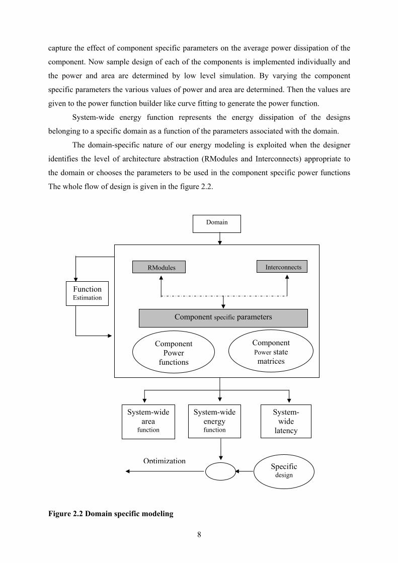
The whole flow of design is given in the figure 2.2.
Figure 2.2 Domain specific modeling
Specific design
Domain
Function Estimation
Interconnects RModules
Component specific parameters
Component Power
functions
Component Power state matrices
System-wide area
function
System-wide energy function
System-wide
latency
Optimization

9
2.2.1.3 Component Power State (CPS) matrices Component Power State (CPS) matrices capture the power state for all the
components in each cycle. For example, in a design that contains k different types of
components (c1..ck) with ni components of type i. If the design has the latency of T cycles,
then k two dimensional matrices are constructed where the i-th matrix is of size T × ni. An
entry in a CPS matrix represents the power state of a component during a specific cycle and
is determined by the algorithm.
Power dissipation by a RModule or Interconnect in a particular state is captured as a
power function of a set of parameters. These functions are typically constructed through
curve fitting based on some sample low-level simulations. CPS matrices contain cycle
specific power state information for each component. The entries in the CPS matrices are
determined by the algorithm.
Combining the CPS matrices and component specific power functions for individual
components, the total energy of the complete system is obtained by summing the energy
dissipation of individual components in each cycle. The system-wide energy function SE is
obtained as:
SE = .1 1 1
1 .ink T
i p psi j t
Cf= = =
⎛ ⎞⎜ ⎟⎝ ⎠
∑ ∑∑ (1)
Where ps = CPS (i.t,j) .
Ci.p.ps is the power dissipated in the j-th component (j = 1...nl) of type i during cycle t (t =
1...T) and f is the operating frequency. CPS (i, t, j) is the power state of the j-th component of
the i-th type during the t-th cycle.
Due to the high-level nature of the model, we can rapidly estimate the system-wide
energy. In the worst case, the complexity of energy estimation is 1
k
il
O T n=
⎛ ⎞×⎜ ⎟⎝ ⎠
∑ which
corresponds to iterating over the elements of the CPS matrices and adding the energy
dissipation by each component in each cycle.
2.2.2 Generation of power functions For estimation of power functions the frame work used here is known MILAN Frame
work .MILAN is a Model based Integrated simulation framework for embedded system
design and optimization by integrating various simulators and tools in to a unified

10
environment. We use the MILAN framework to derive the component specific power
functions associated with the high level energy model.
Figure 2.3 MILAN Framework In order to use the framework, the designer first models the target system using the
modeling paradigms provided in MILAN. The designer provides the architecture and the
parameters (with their possible ranges) that significantly affect the power dissipation of the
component. Model interpreters (MI) in the MILAN are used to drive the integrated tools and
simulators. Model interpreters (MI) translate the information captured in the models into the
format required by the low level simulators and tools. If z(p1, . . . , pn) be the component
specific power function and p1, . . . , pn be the parameters associated with the component.
Figure 2.3 above illustrates the process of deriving component specific power functions. This
process involves estimation of power dissipation through low-level simulation of the
component at different design points. For low-level simulations, we have integrated simulator
such as XPower and ModelSim into the MILAN framework. The switching activity for the
input to the component can be provided by the designer or specified as some default values,
depending on the desired accuracy.
Low-level simulation is performed at each of the chosen design points to estimate the
power dissipation. These power estimates are fed to the power function builder. A typical
low-level simulation for power estimation of a sample design point proceeds as follows. The
Power estimates
Low level simulator (Xpower,
Modelsim)
MILAN
Model Interpreter
Power function builder (curve
fitting)
VHDL code for sample
designs
Architecture, Parameters with ranges of a component
Component specific power
functions

11
chosen sample VHDL design is synthesized using Synopsis FPGA Express on Xilinx
ISE7.1i. The place-and-route file (.ncd file) is obtained for the target FPGA device, Virtex-II
Pro XC2VP4 and ModelSim 5.5e is used to simulate the module and generate simulation
results (.vcd file). These two files are then provided to the Xilinx XPower tool to estimate the
energy dissipation. The power function builder is driven by an MI from the MILAN
framework. For components with a single parameter, the power function can be obtained
from curve-fitting on sample simulation results. In case of larger number of the parameters,
surface fitting can be used. The component specific power function of an interconnect
depends on its length, operating frequency, and the switching activity. Equation (2) is used to
estimate power dissipation in an interconnect. ΦP denotes the power dissipation of a cluster of
k numbers of RModules connected through the candidate interconnects and M.pi represents
power dissipation of the i-th RModule. The power dissipated by the cluster is obtained by
low-level simulation.
1
k
p p pii
IC Mφ=
= −∑ (2)
Figure 2.4 Function generation by Low Level Simulations
Curve fitting
VHDL
XPower
Xilinx Place&Route
Xilinx XST
Synthesis
Candidate Designs
ModelSim
Power
VHDL
Net list
.ncd file
.vcd file
.ncd→VHDArea, Freq. constraints
Low Level Simulation of Candidate Designs
Power functions Pmult,Padd, etc…

12
2.2.3 Power function builder Curve fitting
It is the method of generating the best fit curve that determines the function between
the given parameters. It can be determined by applying least square error method for a no of
differential equations. It can also be determined by using curve fitting tools in MATLAB. So
given the values of the given parameters by the best fit curve it determines the function in
terms of these parameters. It is two types. Parametric and Non parametric.
Parametric fitting is performed by using toolbox library equations (such as linear,
quadratic, higher order polynomials, etc.) or by using custom equations (limited only by the
user's imagination.) A parametric fit would be used to find regression coefficients and the
physical meaning behind them. Non parametric fitting is performed by using a smoothing
spline or various interpolants. A nonparametric fit would be used when regression
coefficients hold no physical significance and are not desired. In this dissertation parametric
curve fitting is used to obtain higher order differential equations.

Chapter 3
Matrix Multiplication

13
3.1Systolic array A systolic array is an arrangement of processors in array where data flows
synchronously across the array between the neighbors, usually with different data flowing in
different directions. Each processor at each step takes in data from one or more neighbors
(e.g. north and west), processes it and, in the next step, outputs result in opposite directions
(south and east).
These have following characteristics.
A specialized form of parallel processing.
Multiple processors connected by short wires.
Processors compute data and store it independently of each other.
3.1 .1 Systolic operation Each unit in a systolic array is an independent processor. Every processor has some
registers and ALU. The cells share information with their neighboring cells, after performing
the needed operation on the data. Some examples of systolic arrays are given below. It is
divided mainly in to two categories. 1-D array and 2-D array. One dimensional array is also
known as linear array.
It consist of three main functional units as shown in figure 3.1
Host Processor:
Controls whole processing.
Controller:
Provides system clock, control signals, input data to systolic array, and
collects results from systolic array.
Systolic array:
Multiple processor network with pipelining.
Some examples of systolic arrays are given in figures 3.2, 3.3 and 3.4. Arrays are classified
depending on how the processors are arranged in the array. It is a network of locally
connected functional units, operating synchronously with multidimensional pipelining

14
Input data
Output data
Systolic array
Controller Host processor
Signals
Figure 3.4 2D systolic triangular array
Figure 3.2 Pipelined linear 1D systolic array
Figure 3.1 Functional units of systolic array
Figure 3.3 2D systolic square array

15
3.1.1.1 Advantages and Disadvantages of Systolic computation Advantages:
Extremely fast.
Easily scalable architecture.
Can do many tasks single processor machines cannot attain.
Turns some exponential problems in to linear or polynomial time.
Systolic arrays are very suitable for VLSI design.
Disadvantages:
Expensive.
Not needed on most applications they are a highly specialized processor type.
3.2 Matrix multiplication algorithm
Let BAC ×= is to be performed.
Where C, A and B are n × n matrices.
Then
kj
n
iikij BAC ∑
=
=1
This can be performed by following algorithm with three no.s of for loops.
Algorithm:
for i : = 1 to n
for j : = 1 to n
for k : = 1 to n
C( i, j ) : = C( i, j ) + A( i, k ) * B( k, j );
(suppose all C( i, j ) = 0 before the computation)
end of k loop
end of j loop
end of i loop
If this algorithm is to be implemented on 2D systolic array its computational complexity will
be O(n3) and it requires n2 no.s of processing elements.

16
3.2.1 Matrix-matrix multiplication on systolic array It can be performed on 2D array or 1D systolic array. Before firing the cell After firing the cell
Figure 3.5 Firing of cells in systolic array
Y
S
S + XY
Y
X X
a11b12+a12b22
a11b11+a12b21
A21b11+a22b21
A21b12+a22b22

17
3.2.1.1 Matrix multiplication on a 2-D systolic array j k j → → → i i k × = ↓ ↓ ↓ a31 a32 a33 a21 a22 a23 ⎯ a11 a12 a13 ⎯ time fronts b11 b12 b21 b13 b22 b31 b23 b32 ⎯ b33 ⎯ ⎯ c33 c32 c31 c23 c13 c22 c21 c12 c11
Figure 3.6 Matrix multiplication on a 2D systolic array
⎥⎥⎥
⎦
⎤
⎢⎢⎢
⎣
⎡
333231
2322 21
131211
a a aa a aa a a
⎥⎥⎥
⎦
⎤
⎢⎢⎢
⎣
⎡
333231
2322 21
131211
b b bb b bb b b
⎥⎥⎥
⎦
⎤
⎢⎢⎢
⎣
⎡
333231
2322 21
131211
c c cc c cc c c
kj

Chapter 4
Energy Efficient
Matrix Multiplication

18
4.1 Introduction Matrix multiplication is a frequently used kernel operation in a wide variety of graphics,
Image processing, robotics, and signal processing applications. Several signal and image
processing operations can be reduced to matrix multiplication. Most previous works on
matrix multiplication on FPGAs focuses on latency optimization. However, since mobile
devices typically operate under various computational requirements and energy constrained
environments, energy is a key performance metric in addition to latency and throughput. So
there is a need of energy efficient design of matrix multiplication algorithms on FPGA.
Hence, the designs would be developed that minimize the energy dissipation. These designs
offer tradeoffs between energy, area, and latency for performing matrix multiplication on
commercially available FPGA devices. Recent efforts by FPGA vendors have resulted in
rapid increase in density of FPGA devices.
So there arises a need for optimization between energy, area and speed for matrix
multiplication on FPGA.
4.2 Methodology adopted
The whole effort is focused on algorithmic techniques to improve energy performance,
instead of low-level (gate-level) optimizations. Various alternative designs are evaluated at
the algorithmic level (with accompanying architectural modifications) on their energy
performance. For this purpose, appropriate energy model is constructed based on a proposed
methodology known as domain specific modeling to represent the impact of changes in the
algorithm on the system-wide energy dissipation, area, and latency. The modeling starts by
identifying parameters whose values change depending on the algorithm and have significant
impact on the system-wide energy dissipation. These parameters depend on the algorithm and
the architecture used and the target FPGA device features. These are known as key
parameters. Closed-form functions are derived representing the system-wide energy
dissipation, area, and latency in terms of the key parameters. The energy, area, and latency
functions provide a high level view to look for possible savings in system-wide energy, area,
and latency. These functions allow making tradeoffs in the early design phase to meet the
constraints. Using the energy functions algorithmic and architectural-level
optimizations are made. To illustrate performance gains low-level simulations are performed
using Xilinx ISE 7.1i and ModelSim 5.5 e, and Virtex-II Pro as an example target FPGA
device. Then Xilinx XPower is used on the simulation data to verify the accuracy of the
energy and area estimated by the functions.
19
Here algorithms and architectures for energy-efficient implementation are presented. An
Energy model specific to this implementation is described. It includes extracting key
parameters from our algorithm and architecture to build a domain-specific energy model and
deriving functions to represent system-wide energy dissipation, area, and latency. Then the
optimization procedure is shown for these algorithms and architectures in an illustrative way.
Analysis of the tradeoffs between system-wide energy, area, and latency is also explained.
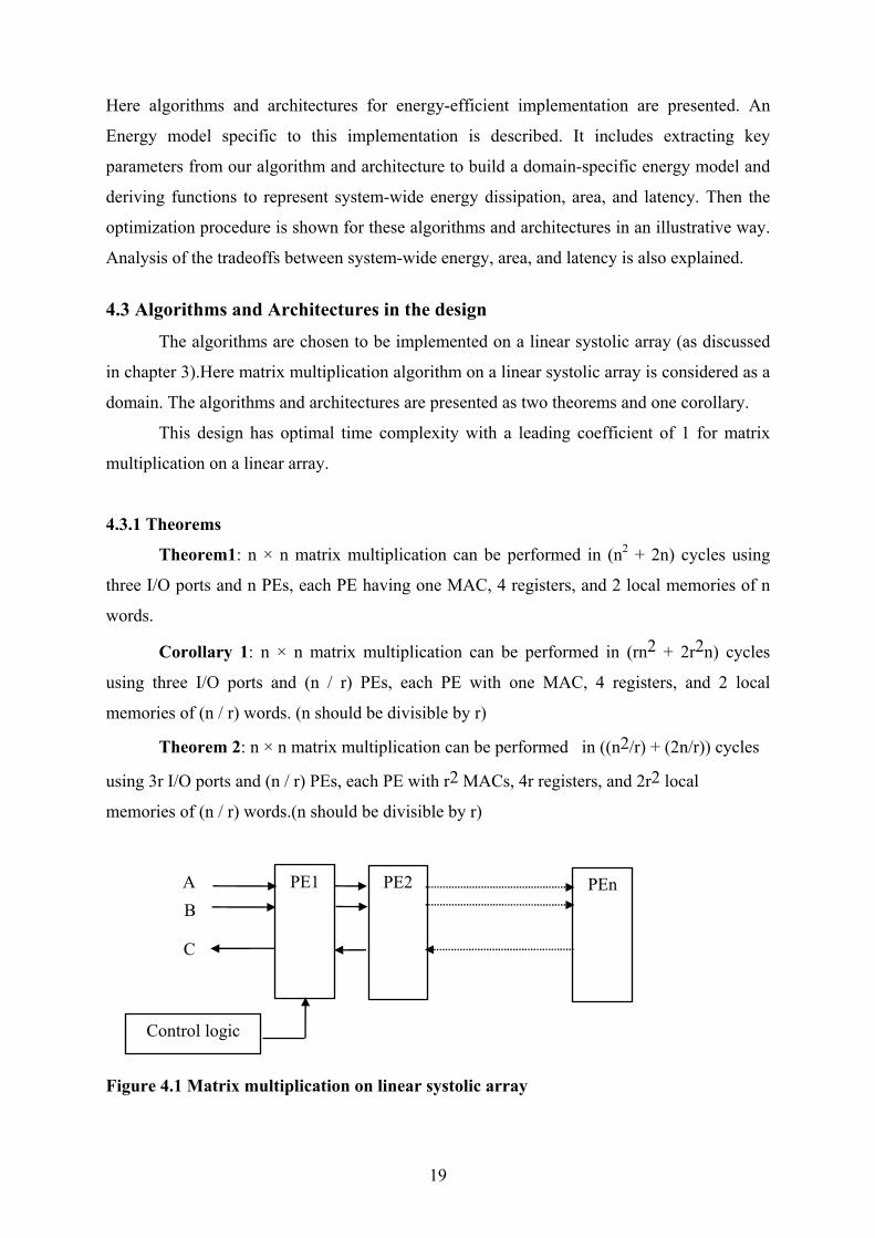
4.3 Algorithms and Architectures in the design
The algorithms are chosen to be implemented on a linear systolic array (as discussed
in chapter 3).Here matrix multiplication algorithm on a linear systolic array is considered as a
domain. The algorithms and architectures are presented as two theorems and one corollary.
This design has optimal time complexity with a leading coefficient of 1 for matrix
multiplication on a linear array.
4.3.1 Theorems
Theorem1: n × n matrix multiplication can be performed in (n2 + 2n) cycles using
three I/O ports and n PEs, each PE having one MAC, 4 registers, and 2 local memories of n
words.
Corollary 1: n × n matrix multiplication can be performed in (rn2 + 2r2n) cycles
using three I/O ports and (n / r) PEs, each PE with one MAC, 4 registers, and 2 local
memories of (n / r) words. (n should be divisible by r)
Theorem 2: n × n matrix multiplication can be performed in ((n2/r) + (2n/r)) cycles
using 3r I/O ports and (n / r) PEs, each PE with r2 MACs, 4r registers, and 2r2 local
memories of (n / r) words.(n should be divisible by r)
Figure 4.1 Matrix multiplication on linear systolic array
B
C
Control logic
A PE1 PE2 PEn

20
Figure 4.2 Architecture of PE for theorem 1
4.3.2 Timing diagrams and explanations
4.3.2.1 Timing steps of theorem 1
During t = 1 to n
For all j, 1 ≤ j ≤n do parallel
PEJ shifts data in BU right to PEJ+1
If (BU =bkj) copy it to BM
During t = n+1 to n2+n
For all j, 1 ≤ j ≤n do parallel
PEJ shifts data in A, BU right to PEJ+1
If (BU = bkj) copy it to BM or BL (alternatively)
If (A = aik)
A
BL
BM
BU
CBUF
COBUF
Ain
Bin
Aout
Bout
Cout Cin
PEJ
From PEJ+1
To PEJ-1
To PEJ+1
From PEJ-1

21
cij’ =cij’ + aik* bkj (bkj is in BM or BL)
(store cij’ in cbuf)
During t = n2+1 to 2n2
For all j, 1 ≤ j ≤n do parallel
PEJ store input Cin to cobuf
PEJ outputs Cij to PEJ-1
PEJ outputs cobuf to PEJ-1
Figure 4.3 Timing diagram of theorem 1(n = 3) 4.3.2.2Explanation of theorem 1: PEJ denotes jth PE from left where j = 1,2…..n. Here PEJ computes jth column of
matrix C i.e. c1j,c2j,c3j…..cnj.which is stored in the local memory Cbuf. In Phase column k of
matrix A and row k of matrix B traverse PE1,PE2,PE3…in order and allows PE J to update
the intermediate value of C’ij = C’ij + Aik *Bkj.in order and allow to update , where C’ij
represents the intermediate value of Cij. Once bkj arrives at PEJ a copy of resides in until
a1k,a2k,a3k……..ank passes through it. It is observed that the following two essential
requirements should be satisfied: 1) Since aik stays at each PEJ for just one cycle, bkj should
arrive at no later than , aik for any value of i, and 2) Once bkj arrives at PEJ , a copy of it
should reside in it until ank arrives. These two essential requirements for this systolic

22
implementation are satisfied with a minimal number of registers. In addition, the number of
cycles required to finish the operation and the amount of local memory per PE are evaluated.
1) Since aik stays at each PEJ for just one cycle, bkj should arrive at no later than
, aik.for any value of i: Matrix B is fed to the lower I/O port of [Figure 4.2] in row major
order as b11,b12,b13…. and . Matrix A is fed to the upper I/O port of in column major order as
a11,a21,a31…….. n cycles behind Matrix B. For example,a11 is fed to the upper I/O port of in
the same cycle as b21 is fed to the lower I/O port of PE1. The number of cycles required for bkj
to arrive at PEJ is (k-1)n+2j-1. aik requires n+ (k-1)n+i+j-1 cycles to arrive at PEJ. The
requirement is satisfied since (k-1)n+2j-1 ≤ n+ (k-1)n+i+j-1 for all i and j.
2) Once bkj arrives at PEJ , a copy of it resides in it until ank arrives.: The registers
are minimized to store copies of bkj (k = 1,2,3….n) in PEJ.. Here two registers [denoted BM
and BL in Fig. 4.2] are sufficient to hold bkj at PEJ.(to store two consecutive elements,bkj and
b(k+1)j).. In general, bkj is needed until ank arrives at PEJ at the n+ (k-1)n+n+j-1-th cycle. b(k+2)j
arrives at PEJ in the (k+1)n+2j-1 th cycle. Since (k+1)n+2j-1 > n+ (k-1)n+n+j-1for all i,j and
k .So b(k+2)j can replace bkj.So two registers are sufficient to hold the values.
3) n2+2n cycles are needed to complete the matrix multiplication. The computation
finishes one cycle after ann arrives at n, which is the n2+2n -1-th cycle. Column j of the
resulting output matrix C is in cbuf of PEJ , for 1≤j≤n. To move the matrix C out of the array,
an extra local memory cobuf and two ports Cout and Cin are used in each PE.
4.3.2.3 Explanation of corollary 1:
Any n × n matrix multiplication can be decomposed in to r3 numbers of (n/r) × (n/r) matrix
multiplications .So multiplication can be done in r3 ×((n/r)2 + 2(n/r)) i.e. same as (rn2 +
2r2n). By replacing n with (n/r) in the proof of theorem1 corollary1 can be proved easily and
formula for it’s latency can be obtained.

23
Figure 4.4 (Architecture of PE for theorem 2)
4.3.2.4Timing steps of theorem 2
Completing multiplication
During t = 1 to n /2
For all j do in parallel
PEJ shifts words in BU1 & BU2 to PEJ+1
If (BU1 = b11kj) copy it to BM1
If (BU2 = b12kj) copy it to BM2
During t = (n /2+1) to ((n/2)2+(n/2))
For all j do in parallel
PEJ shifts A1,A2,BU1,BU2 to the right(PEJ+1)
If( BU1 = b11kj) copy it to BM1(after moving BM1 to BL1)
If( BU2 = b12kj) copy it to BM2(after moving BM2 to BL2)
If(A1 = a11ik)
cbuf11=cbuf11 + a11ik ×b11kj
B2out
A1
A2
BU1 BM1 BL1
BU2 BM2 BL2
CIJ’ CIJ’ CIJ’
COBU COBU COBUCOBU
A1in
A2in
B2in
C1out
C2out
A1in
B1in
C1in C2in
B1in
CIJ’
From PEj+1
To PEj+1
A2out
From PEj-1
To PEj-1

24
cbuf12=cbuf12 +a11ik × b12kj
If(A2 = a21ik)
cbuf21=cbuf21+a21ik × b11kj
cbuf22=cbuf22+a21ik × b12kj
During t = (n /2)2+1 to (2(n/2)2+n)
For all j do in parallel
Repeat for b21kj,b22kj, and a12kj,a22kj
Outputting result
During t = (n 2/2+1) to (2n2/2)
For all j do in parallel
PEj outputs c11ij’(from MAC11) to c1out.
c12ij’(from MAC12) to c2out.
PEj stores c21ij’(from MAC 21) to cobuf21.
c22ij’(from MAC 22) to cobuf22.
PEJ store c1in to cobuf11
& c2in to cobuf12
PEJ output cobuf21 to c1out
& cobuf22 to c2out
PEJ outputs cobuf11 to c1out
& cobuf12 to c2out
4.4 Word width Decomposition technique
In all the above procedure the input word width is taken directly. So when the width
of the word increases the size of the multiplier increases to a large extent. When input word is
considered directly and the size of scalar multipliers can be significantly large for practical
VLSI implementation when the input word-width increases. So to overcome this problem a
technique is used that subdivides the width of the word and a smaller numbers of fixed sized
multipliers are used to generate the partial results and finally they are added to get the final
result. It provides structural flexibility, what ever the size of word the multiplier size remains
fixed.
The architecture for word width decomposition technique is explained below.

25
4.4.1Architecture with word width decomposition technique The whole architecture consists of a decomposition unit, a composition unit and basic
operators (fixed sized multipliers and Muxes) in addition to previous architecture in a
processing element.
Figure 4.5 Decomposition unit
The overall operation is based on two basic assumptions.(1) Matrix multiplication is
performed on N×N matrices where N is a power of 3. (2) Each element in the matrices is a
fixed-point integer with word-width of W. Initially, N×N matrix multiplication is
decomposed into several 3× 3 matrix multiplications.
This process is illustrated with as N = 6.
Where A1, B1, A2 and B2 are 3×3 matrices. After the initial decomposition, all matrix
multiplications are 3×3 matrix multiplications where word-width of each element is W.

26
A1B1 = (QA1QB12P + QA1RB1 + RA1QB1 )2P + RA1RB1
Where, QA1QB1, QA1RB1, RA1QB1, RA1RB1 and represent decomposed 3×3 matrix
multiplications. Two matrices, QA1 andQB1 are decomposed further until each element in all
the decomposed matrices is less than 2p where all elements are represented with p-bit
precision. Upon completion of the decomposition process, all matrix multiplications with p-
bit precision are computed in parallel with much smaller scalar multipliers than W. The
outputs from this computation are accumulated to generate the final outputs for one 3×3 -bit
matrix multiplication. After repeating the same process, the outputs for matrix multiplications
are constructed.
4.4.1.1 Procedure of decomposition There are two ways to decompose the matrices. The first approach is to divide the
width of the original elements successively in half. This approach, called balanced word-
width decomposition, is illustrated in Fig. 4.5. If p be a finite number represent the
decomposed data width, then, a multiplication by 2p becomes a simple p-bit shift. Initially,
the matrix multiplication with W–bit input elements is decomposed into two sub matrix
multiplications. Then, the decomposed matrix multiplication is further decomposed until the
element word length is less than or equal to p. After the decomposition, there will be many
but smaller sub matrix multiplications which can be performed with simple arithmetic units.
The depth of the decomposition tree depends on the word length of the original data element.
The restriction with this approach is that the size W of must be p.2i, where i is an integer. The
second approach, skewed word-width decomposition, relaxes this restriction and the input
elements bits can be decomposed at a time, starting from either the least significant bits of the
element or the most significant bits of the element. Thus, the original word length can be any
multiple of p. The illustrations shown in Fig 4.5 may seem to suggest that the decomposition
process takes multiple stages of operations. The decomposition of the original matrix
multiplication results in 16 sub matrix multiplications (i.e. for W =16 and p = 4). But the
actual decomposition can be done directly from the input elements and the decomposition
processes illustrated above, are handled during the composition where siftings and
summations are performed. Basically, the decomposition process is merely dividing the
original values through interconnection distribution.

27
4.4.1.2 Supporting two’s complement data:
The decomposition unit must support word-width decomposition of 2’s complement
numbers. This is done by incorporating an adder for each -bit segment of the original element
as shown in Fig. 4.6. If the original input element is a negative number, a sign bit of the
original element is appended to each p-bit segment to form a p+1-bit segment. Then, 1 is
added to this value and its overflow bit is ignored. Such addition is not necessary for the least
significant -bits. The sign bit is overwritten if the p-bit element is all zero. No conversion is
necessary if the original elements are positive. A multiplexor is used for selection.
Figure 4.6 Mechanism to support two’ complement data
4.4.1.3 Composition Unit:
In the balanced decomposition with W = 16 and p = 4 .Then after the decomposition, the
matrix multiplication is represented as AB = (QQAQQB)26P + (QQARQB)25P+ (RQAQQB)25P + (RQARQB)24P + (QRAQQB)24P + (RRAQQB)
23P + (RRAQQB )23P + (RRARQB)22P + (QQAQRB)24P + (QQARRB) 23P + (RQAQQB )23P+ (RQARRB)
22P + (QRAQRB)22P + (QRARRB) 2P + (RRAQRB )2P + (RRARRB) .
The original matrix multiplication A×B consists of many smaller sub matrix multiplications,
which can be computed in parallel with the same hardware. The results from these smaller
matrix multiplications are the partial results for Cij where they are accumulated by an adder
tree to generate the outputs of the matrix multiplication. Hence, the adder tree is executed
four times to generate a complete 3×3 output matrix.

28
Figure 4.7 Composition Unit for W= 16 and P = 4
4.4.1.3 Construction of theorem 1 with word width decomposition technique
In the processing element used in theorem 1 two extra components are added along
with the previous architecture. The matrices A and B are entered column and row wise. Then
placed in the registers as before. But before giving to the multipliers these are given to the
decomposition unit as described in Fig 4.5 .The decomposed data are given to a set of smaller
width (p bit, here p = 4) multipliers. Multipliers frequency is chosen to be 4 times faster than
decomposition unit and composition unit. While decomposition unit and composition unit
operates in the same clock frequency. So four numbers of multipliers can generate 16 partial
products at each Tdecomp. So after each Tdecomp the datas are fed to composition unit to generate
the final result. All other operations are same as before.
So along with the pipelining scheme this technique functions properly and generates
results with the same latency. The architecture for one processing element is given in the
figure 4.8.

29
Figure 4.8 Theorem 1 with word width decomposition
4.5 Construction of High level energy model
This model is applicable only to the design domain spanned by the family of
algorithms and architectures being evaluated. The family represents a set of algorithm-
architecture pairs that exhibit a common structure and similar data movement. Domain is a
set of point designs resulting from unique combinations of algorithm and architecture-level
changes. Key parameters are extracted considering their expected impact on the total energy
performance. For Example, if the number of MACs and the number of registers change
values in a domain and are expected to be frequently accessed, a domain-specific energy
model is built using them as key parameters. The parameters may include elements at the
gate, register, or system level as needed by the domain. It is a knowledge-based model that
exploits the knowledge of the designer about the algorithm and the architecture. This
knowledge is used to derive functions that represent energy dissipation, area, and latency.
Aout
Bout
sram Cin 16 numbers of accumulators
A
BL BM BU
Ain
Bin
Decomposition network
Cout
Composition network
mult mult mult mult
16 numbers of 8 bit SRAM each with 3 entries
16 products

30
Beyond the simple complexity analysis, we make the functions as accurate as possible by
incorporating implementation and target device details. For example, if the number of MACs
is a key parameter, then a sample MAC is implemented on the target FPGA device to
estimate its average power dissipation. A power function representing the power dissipation
as a function of, the number of MACs is generated. This power function is obtained for each
module related to the key parameters.
An energy model specific to the domain is constructed at the module level by
assuming that each module of a given type (register, multiplier, SRAM, BRAM, or I/O port)
dissipates the same power independent of its location on the chip. This model simplifies the
derivation of system-wide energy dissipation functions. The energy dissipation for each
module can be determined by counting the number of cycles the module stays in each power
state and low-level estimation of the power used by the module in the power state, assuming
average switching activity. Table 4.1 below gives the key parameters and the number of each
key module in terms of the two parameters for each domain.
4.5.1 Generation of energy, area and latency functions Functions that represent the energy dissipation, area, and latency are derived for
Corollary 1 and Theorem 2 along with word width decomposition technique. The energy
function of a design is approximated to be i ii
PT∑ , where Ti and Pi represent the number of
active cycles and average power for module. For example, denotes the average power
dissipation of the multiplier module. The average power is obtained from low-level power
simulation of the module. The area function is given by, ii
A∑ where Ai represents the area
used by module. In general, these simplified energy and area functions may not be able to
capture all of the implementation details needed for accurate estimation. But here
algorithmic-level comparisons are concerned, rather than accurate estimation. Moreover, the
architectures are simple and have regular interconnections, and so the error between these
functions and the actual values based on low-level simulation is expected to be small. The
latency functions are obtained easily because the theorems and corollaries already give the
latency in clock cycles for the different designs.

31
Figure 4.9 generation of energy and area functions
In this case each of these theorems uses a similar method of data transfer between processing
elements on linear systolic array. So these algorithms and architectures implementing the
matrix multiplication create a domain. In this domain the basic building blocks (components)
are the MACs (multipliers and adders) ,registers ,memories(Slice based RAM or Block
RAM) and I/Os. With insertion of word width decomposition technique two additional
components are added i.e. decomposition unit and composition unit.
The key parameters are n and r. The component specific parameters are no. of
entries(x) (in case of memory only) and precision (w) .So power/area functions for
components are generated in terms of these parameters. Then system wide energy, area and
latency functions are generated by combination of power/area functions and key parameters.
Kernels
Domain1, Algorithm1, Architecture1 (Range of key parameters)
e.g. matrix multiplication or FFT or DCT
system wide energy, Area & latency
functions. (with key parameters)
component1 component2
Component specific parameters
VHDL code for
Rmodules
Power function builder (Curve fitting)
In mat lab
Others domains
Synthesis and Simulation in (ModelSim,
Isim) Power
Estimation With excel sheet or
XPower
Component Specific power functions
(with random input vectors)

32
The functions in Table 4.1 and table 4.2 can be used to identify tradeoffs among energy, area,
and latency for various designs.
Table 4.1 Functions for theorem1 and theorem 2
Latency (cycles)
L = r3{(n/r)2 +2 (n/r)}
Energy
L{(n/r)[(w/k)Pmult+Psram+(w/k)2Padd+(w/k)2Psram
+Pcomp+Pdcomp+4Pr] +2PI+PO+ (n/r)Pcnt}
Area
(n/r) {(w/k)Amult+Asram+(w/k)2Aadd++(w/k)2Asram+4Ar+Acnt}
Table 4.2 Functions for theorem1+ word width decomposition
A2=nr(Amult+Aadd+2Asram)+n(4Ar)+nrAcnt
Area
E2 = L2{nr(Pmult+Padd+2Psram)+n(4Pr) +2rpi+rpo+nrPcnt} Energy
L2 = (n2/r) + (2n/r) Latency (cycles)
Performance model metric
Key parameters : n & r
Theorem 2
A1 = (n/r)(Amult+Aadd+2Asram+4Ar)+Acnt Area
E1 = L1{(n/r)(Pmult+Padd+2Psram+4Pr)+2pi+po+(n/r)Pcnt} Energy
L1 = r3{(n/r)2 +2 (n/r)} Latency (cycles)
Performance model metric
Key parameters n , r
Corollary 1

33
4.6 Results and discussion
4.6.1 Functions generation from curve fitting
4.6.1.1 The curve fitting is used in MATLAB to generate power and area functions for the
designs.
0 10 20 30 40 50 60 700
10
20
30
40
50
60
70
precision w
power
add
er
best fit curve
0 10 20 30 40 50 60 700
5
10
15
20
25
30
precision w
area
reg
iste
r
best fit curve
Figure 4.10 Best fit curves to generate power, area functions using curve flitting

34
Each of the component is simulated individually and area or power values obtained by
varying the component specific parameters (precision (w) and no. of entries(x)).These values
are given to power function builder to generate area and power functions in terms of
component specific parameters. W is varied as 4, 8, 16, 32 and 64. The result from simulation
with these values of W is given to power function builder curve fitting to generate the
functions through best fit curve.
Timing diagram of theorem 1 with word width decomposition (from simulation)

35
4.6.2 Comparison of design at high level
Combining these component specific power and area functions and key parameters
the system wide energy, area and latency functions is generated (Table 4.1 and 4.2).So by
varying the component specific parameters the results (energy, area and latency) are obtained
at high level. (Table 4.3 and 4.4) These results can be used for determining optimized design
at algorithm level without going for low level simulation. Suppose the latency and energy
dissipation are constrained then depending upon the constraints the suitable design can be
selected from table with least area.
Theorem 1: By varying the block size (n/r) the values of energy, area and latency are
obtained from the functions generated by curve fitting . Design
Metric
3×3
6×6
12×12
Block size (n/r)
3 6 12
Energy (nj)
61.9
179.6
689
Latency (us)
0.06
0.24
0.96
Them 1 +
WWD
Area (slices)
684
1376
3495
Table 4.3Results for theorem 1 with word width decomposition (w = 16 and k =4)
Theorem 2: By varying the block size (n/r) the values of energy, area and latency are
obtained from the functions generated by curve fitting. Design
Metric
6×6
12×12
24×24
Block size (n/r)
3 (r =2) 6 (r = 2) 6 (r = 4 )
Energy (nj)
157 1324 4438
Latency (us)
0.12 0.33 0.69
Theorem
2 + WWD
Area (slices)
3944 9469 9469
Table 4.4 Results for theorem 2 with word width decomposition (w = 16 and k =4)

36
4.6.3 Estimation of error at low level
Theorem1 Theorem1 + word width decomposition
Error for 2nd
column (%)
Reduce/increase
(%) for 1st and 2nd
column.
W = 16 W = 16, k = 4
Area = 517slices Area = 709slices.
3.52 27 % increased
Latency = 0.06us Latency = 0.06us
No error No change
Energy = 49nj Energy = 67nj
7.6 26 % increased
W = 64 W = 64, k = 16
Area = 9432slices Area = 4760 slices.
11.3 49% reduced
Latency = 0.06us Latency = 0.06us No error No change
Energy = 291nj Energy = 123nj
13.9 57% reduced
Table 4.5 Comparison of result with and without word width decomposition technique from low level simulation for n = 3 4.6.4 Conclusion
Optimization at high level
From table 4.3 and 4.4 it is shown that the values of energy, area and latency can be obtained
for theorems with word width decomposition technique from the functions generated by
curve fitting .So depending on the requirement the optimized design can be chosen at high
level. In theorem 1 pipelining is used and theorem 1 pipelining is used with parallel
processing. So as per results when low latency is required with some increased source then
theorem 2 is chosen, When limited resources are available theorem 1 is chosen with increased
latency. The results obtained from functions generated at high level are compared with
simulated values obtained at low level and the error is found to be within 15%. The values are
compared with the values in theorem 1 with and without word width decomposition (Table
4.5).It concludes the word width decomposition technique reduces the area and energy
without change in the latency with large precision of word. For precision less than 16 bits it
does not give better result. But for precision greater than 16 bits(as 64 bits) it reduces area
and energy dissipation to a great extent. Since the whole design is pipelined throughput is
good.

Chapter 5
The Fast Fourier Tranform

37
5.1 Introduction
This chapter begins with an overview of Fourier transform in most common form the
Discrete Fourier Transform (DFT). Remainder of the chapter focuses on the introduction of a
collection of algorithms used to efficiently compute the DFT; these algorithms are known as Fast
Fourier Transform (FFT) algorithms.
5.2The Discrete Fourier Transform (DFT)
The discrete Fourier transform operates on an N-point sequence of numbers, referred to
as x(n). This sequence can (usually) be thought of as a uniformly sampled version of a finite
period of the continuous function f(x). The DFT of x(n) is also an N-point sequence, written
as X(k), and is defined in Eq. 5.1. The functions x(n) and X(k) are, in general, complex. The
indices n and k are real integers. 1
2 /
0( ) ( ) ,
Ni nk N
nX k x n e π
−−
=
= ∑ k = 0,1,………N - 1 (5.1)
Using a more compact notation, can also be written, 1
0( ) ( ) ,
Nnk
Nn
X k x n W−
=
=∑ k = 0,1,………N - 1 (5.2)
Introducing the terms 2 /i N
NW e π−= (5.3)
2 2cos siniN Nπ π⎛ ⎞ ⎛ ⎞= −⎜ ⎟ ⎜ ⎟
⎝ ⎠ ⎝ ⎠ (5.4)
The variable WN is often called an “Nth root of unity” since (WN) = 2ie π− = 1. Another
very special quality of WN is that it is periodic; that is, n n mNN NW W += for any integer m. The
periodicity can be expressed through the relationship n mN n mNN N NW W W+ = because,
( )2 / , ,.......... 1,0,1.......mNmN i N
NW e mπ−= = −∞ − ∞ (5.5)
2i me π−= (5.6)
= 1 (5.7)

38
In a manner similar to the inverse continuous Fourier transform, the Inverse DFT
(IDFT), which transforms the sequence X(k) back into x(n), is, 1
2 /
0
1( ) ( ) , 0,1........., 1N
i nk N
kx n X k e n N
Nπ
−
=
= = −∑ (5.8)
1
0
1 ( ) , 0,1........., 1N
nkN
kX k W n N
N
−−
=
= = −∑ (5.9)
From Eqs. 5.2 and 5.9, x(n) and X(k) are explicitly defined over only the finite interval
from 0 to N-1. However, since x(n) and X(k) are periodic in N, (viz., x(n) = x(n + mN) and
X(k) = X(k + mN) for any integer m), they also exist for all n and k respectively.
An important characteristic of the DFT is the number of operations required to
compute the DFT of a sequence. Equation 5.2 shows that each of the N outputs of the DFT is
the sum of N terms consisting of x(n) nkNW products. When the term nk
NW is considered a pre-
computed constant, calculation of the DFT requires N (N - 1) complex additions and N2
complex multiplications. Therefore, roughly 2N2 or O(N2) operations1 are required to calculate
the DFT of a length-N sequence.
For this analysis, the IDFT is considered to require the same amount of computation
as its forward counterpart, since it differs only by a multiplication of the constant 1/N and by
a minus sign in the exponent of e. The negative exponent can be handled without any
additional computation by modifying the pre-computed WN term.
Another important characteristic of DFT algorithms is the size of the memory required
for their computation. Using Eq. 5.2, each term of the input sequence must be preserved until
the last term has been computed. Therefore a minimum, 2N memory locations are necessary
for the direct calculation of the DFT.
5.3 The Fast Fourier Transform
FFT is used to speed up the DFT. Instead of direct implementation of the
computationally intensive DFT, the FFT algorithm is used to factorize a large point DFT
recursively into small point DFTs such that the overall operations involved can be drastically
reduced.
1 The symbol O means “on the order of”; therefore, O(P) means on the order of P.

39
5.3.1 Cooley Tukey algorithm
This is a divide and conquer algorithm that recursively breaks down a DFT of any
composite size N = N1N2 into many smaller DFT of sizes N1 and N2, along with O(N)
multiplications by complex roots of unity traditionally called twiddle factors (after
Gentleman and Sande, 1966).This method (and the general idea of an FFT) was popularized
by a publication of and J. W. Cooley and J.W.Tukey in1965, but it was later discovered that
those two authors had independently re-invented an algorithm known to Carl Fredrick Gauss
around 1805 (and subsequently rediscovered several times in limited forms).
The most well-known use of the Cooley-Tukey algorithm is to divide the transform
into two pieces of size N / 2 at each step, and is therefore limited to power-of-two sizes, but
any factorization can be used in general (as was known to both Gauss and Cooley/Tukey).
These are called the radix-2 and mixed-radix cases, respectively (and other variants such as
the split radix FFT have their own names as well). Although the basic idea is recursive, most
traditional implementations rearrange the algorithm to avoid explicit recursion. Also, because
the Cooley-Tukey algorithm breaks the DFT into smaller DFT, it can be combined arbitrarily
with any other algorithm for the DFT, such as those described below.
More generally, Cooley-Tukey algorithms recursively re-express a DFT of a composite
size N = N1N2 as:
Perform N1 DFT of size N2.
Multiply by complex roots of unity called twiddle factors.
Perform N2 DFT of size N1.
Typically, either N1 or N2 is a small factor (not necessarily prime), called the radix
(which can differ between stages of the recursion). If N1 is the radix, it is called decimation in
time (DIT) algorithm, whereas if N2 is the radix, it is decimation in frequency (DIF, also
called the Sande-Tukey algorithm). The version presented above was a radix-2 DIT
algorithm; in the final expression, the phase multiplying the odd transform is the twiddle
factor, and the +/- combination (butterfly) of the even and odd transforms is a size-2 DFT.
(The radix's small DFT is sometimes known as a butterfly, so-called because of the shape of
the dataflow diagram for the radix-2 case.)
5.3.1.1 Data reordering and bit reversal The most well-known reordering technique involves explicit bit reversal for in-place
radix-2 algorithms. Bit reversal is the permutation where the data at an index n, written in
binary with digits b4b3b2b1b0 (e.g. 5 digits for N=32 inputs), is transferred to the index with
reversed digits b0b1b2b3b4. In the last stage of a radix-2 DIT algorithm like the one presented

40
above, where the output is written in-place over the input: when Ek and Ok are combined with
a size-2 DFT, those two values are overwritten by the outputs. However, the two output
values should go in the first and second halves of the output array, corresponding to the most
significant bit b4 (for N=32); whereas the two inputs Ek and Ok are interleaved in the even and
odd elements, corresponding to the least significant bit b0. Thus, in order to get the output in
the correct place, these two bits must be swapped in the input.
5.3.2 Radix 2 FFT algorithm
Many FFT users, however, prefer natural-order outputs, and a separate, explicit bit-
reversal stage can have a non-negligible impact on the computation time, even though bit
reversal can be done in O(N) time and has been the subject of much research (e.g. Karp,
1996; Carter, 1998; and Rubio, 2002). Also, while the permutation is a bit reversal in the
radix-2 case, it is more generally an arbitrary (mixed-base) digit reversal for the mixed-radix
case, and the permutation algorithms become more complicated to implement. Moreover, it is
desirable on many hardware architectures to re-order intermediate stages of the FFT
algorithm so that they operate on consecutive (or at least more localized) data elements. To
these ends, a number of alternative implementation schemes have been devised for the
Cooley-Tukey algorithm that do not require separate bit reversal and/or involve additional
permutations at intermediate stages.
For simplicity, N is chosen to be a power of 2 (N= 2m), where m is a positive integer.
With this assumption, it is possible to break x(n) of length N into two sequence of lengths N/2.
The first sequence xeven(m) contains all even samples of x(n) and the second sequence xodd(m)
contains all the odd samples. Equation 5.2 can now be written as follows:
( )2 1
0 1( ) ( )
even odd
N Nnk nk
N Nn n
X K x n W x n W− −
= =
= +∑ ∑ (5.10)
If 2m and 2m+1 are substituted for n in the even and odd summations respectively,
then equation 5.10 can be written as follows:
( )/ 2 1 / 2 1
2 2
0 0(2 ) ( ) (2 1) ( )
N Nmk mk k
N N Nm m
X K x m W x m W W− −
= =
= + +∑ ∑ (5.11)
But 2/ 2N NW W= and hence,

41
( )/ 2 1 / 2 1
/ 2 / 20 0
(2 ) (2 1)N N
mk mkN N
m mX K x m W x m W
− −
= =
= + +∑ ∑ (5.12)
Equation 5.12 can also be written in terms of even and odd DFTs as follows:
( ) ( ) ( )keven N oddx k F k W F k= + (5.13)
The equation on the right hand side of the equation 5.16 corresponds to N/2 point
DFTs of even (Feven (k)) and odd (Fodd(k)) parts of x(n). The direct computation of Feven (k)
requires (N/2)2 complex multiplications. The same is true for Fodd(k). Moreover, there are N/2
additional complex multiplications required to compute kNW Fodd (k). Hence the computation of
X(k) requires 2(N/2)2 + N/2 complex multiplication. For large N, about 50% multiplication
operation savings can be achieved compared to the direct calculation of the DFT by the
equation 5.2.
Figure 5.1: Dataflow graph of an 8-point radix-2 two N/2 point FFT
The dataflow of this algorithm for N=8 is shown in Figure 5.1. The horizontal axes
signify the computational stages. The vertical axes indicates the memory location of the
memory which is required for storing the sequence x(n). In Figure 5.1, following N/2-point
DFTs (here, N/2 is 4) the data will be multiplied by 8kW . The calculations after the 8
kW
multiplications are the 2-point DFTs. There, the minus (-) sign adjacent signifies that the
4 point
FFT
4 point FFT
x (0)
x (2)
x (4)
x (6)
x (1)
x (3)
x (5)
x (7)
X (0)
X (1)
X (2)
X (3)
X (4)
X (5)
X (6) X (7)
W80
W81
W82
W83

42
signal is subtracted from the node. Otherwise the signal will be summed into that node. The
number of FFT points N is chosen to be the power of 2 and if N is greater than 2 then Xeven
(m) and Xodd(m) also have even number of points. Hence they can be further decimate in there
even and odd sequences and computed from the N/4-point FFTs. Repeating this decimation
procedure for log2(N) - 1 times until sequences with only two components are gained in the
last stage.
A total of log2(N) stages can be produced by applying this decimation procedure. Each
stage has N/2 complex multiplications by some power of NW . The final stage is reduced to 2-
point DFT where no multiplication is required, since the twiddle factors are trivial numbers
there. The input sequence is broken into two smaller sequences at each stage; hence radix-2
FFT algorithm is called Decimation in time .Hence a total number of only (N/2)log2(N)
complex multiplications are needed for computing an N-point FFT.
Besides the radix-2 FFT algorithm, the second popular radix-2 FFT algorithm is
known as decimation in frequency (DIF) FFT. The decimation in frequency can be obtained
by slightly modifying the procedures the decimation in time algorithm. In this algorithm the
input data is separated into its first N/2 and its last N/2 components instead of even and odd
components. The name decimation in frequency originated from the fact that this decimation
leads to the bit reversal of the DFT vector. The figure 5.2 and 5.3 shows the data flow in both
the algorithms.
Figure 5.2: Dataflow graph of an 8-point radix-2 decimation in time FFT

43
Figure 5.3: Dataflow graph of an 8-point radix-2 decimation in frequency FFT .
Figure 5.4: Flow graph of a 16-point radix-4 decimation-in-time FFT algorithm.
5.3.3 Radix-4 FFT Algorithm
When the number of data points N in the DFT is a power of 4(N = 4v), then it is more
efficient computationally to employ a radix-4 algorithm instead of a radix-2 algorithm. A
radix-4 decimation-in-time FFT algorithm is obtained by splitting the N-point input sequence
x(n)into four sub sequences x(4n), x(4n + 1), x(4n + 2) and x(4n + 3). The radix-4 decimation
in- time FFT algorithm is obtained by selecting L = 4 and M = N/4 in the unified approach.
This leads to n = 4m + l and k = (N=4)p + q. The radix-4 algorithm is obtained by following

44
the decomposition procedure outlined in the previous section v time's recursively. The
signal flow graph of a 16-point radix-4 decimation-in-time algorithm is shown in Figure 5.4
5.3.3.1 DECIMATION IN TIME (DIT):
∑∑
∑∑−
=
−
=
−
=
−
=
++++
++=
14/
04/
314/
04/
2
14/
04/
114/
04/
)34()14(
)14()4()(
N
NNN
N
NNN
N
NNN
N
NN
WnxWWnxW
WnxWWnxKX (5.14)
5.3.3.2 DECIMATION IN FREQUENCY (DIF):
14
0/ 4
0
14
/ 40
3(4 ) ( )4 2 4
3(4 1) ( )4 2 4
3(4 2) ( )4 2 4
N
knN N
n
N
n knN N
n
n
N N NX k x n x n x n x n W W
N N NX k x n j x n x n jx n W W
N N NX k x n x n x n x n
−
=
−
=
⎡ ⎤⎛ ⎞ ⎛ ⎞ ⎛ ⎞= + + + + + +⎜ ⎟ ⎜ ⎟ ⎜ ⎟⎢ ⎥⎝ ⎠ ⎝ ⎠ ⎝ ⎠⎣ ⎦
⎡ ⎤⎛ ⎞ ⎛ ⎞ ⎛ ⎞+ = − + − + + +⎜ ⎟ ⎜ ⎟ ⎜ ⎟⎢ ⎥⎝ ⎠ ⎝ ⎠ ⎝ ⎠⎣ ⎦
⎡ ⎤⎛ ⎞ ⎛ ⎞ ⎛ ⎞+ = − + + + − +⎜ ⎟ ⎜ ⎟ ⎜ ⎟⎢ ⎥⎝ ⎠ ⎝ ⎠ ⎝ ⎠⎣ ⎦
∑
∑1
42
/ 40
14
3/ 4
0
3(4 3) ( )4 2 4
N
n knN N
N
n knN N
n
W W
N N NX k x n j x n x n jx n W W
−
=
−
=
⎡ ⎤⎛ ⎞ ⎛ ⎞ ⎛ ⎞+ = + + − + − +⎜ ⎟ ⎜ ⎟ ⎜ ⎟⎢ ⎥⎝ ⎠ ⎝ ⎠ ⎝ ⎠⎣ ⎦
∑
∑
(5.15)
The radix-4 butterfly, shown in Figure 5.5, is constructed by merging 4-point DFT
with associated coefficients between DFT stages. The four outputs of the radix-4 butterfly
namely BO1, BO2, BO3 and BO4 are expressed in terms of its inputs BI1, BI2, BI3 and BI4 as
follows:
BO1 = BI1 + BI2W1 + BI3xW2 + BI4W3
BO2 = BI1 - iBI2W1 - BI3W2 + iBI4W3
BO3 = BI1 - iBI2W1 + BI3W2 - BI4W3
BO4 = BI1 + iBI2W1 - BI3W2 - iBI4W3
(5.16)

45
Figure 5.5: Radix-4 decimation in time butterfly.
The radix-4 butterfly requires three complex multiplications. The multiplication with
TW is accomplished by negation and swapping of the real and imaginary parts. Radix-4 has a
computational advantage over radix-2 because radix-4 butterfly does the work of four radix-2
butterflies using three multipliers instead of four multipliers in four radix-2 butterflies. On the
negative side, a radix-4 butterfly is more complicated to implement than a radix-2 butterfly.
While radix-2 and radix-4 FFTs are certainly the most widely known algorithms, it is
also possible to design FFTs with even higher radix butterflies. They are not often used
because the control and dataflow of their butterflies are more complicated and the additional
efficiency gained diminishes rapidly for radices greater than four.
To see this intuitively, let us choose N = 64 and do the FFT three ways, by radix 2,
radix 4, and radix 8, and count the number of complex multiplications needed for each case.
1. In radix 2, if we are doing DIT, the first stage consists of multiplications by W0 = 1, or no
multiplications. The second stage has twiddles W0 and W16 = j so again no multiplications.
The third stage has one-half of full the full complement multiplications and so on. As a
formula, we can write
2 2log 2 (log 1)
2 11
2 1 1 2(log 2) 12 2 2 2 1 2
N Nn
N nn
N N NM N− − −
−=
⎡ ⎤− −= = − − +⎢ ⎥−⎣ ⎦
∑
(5.17)
where MN is the number of complex multiplications needed for an N-point radix 2 FFT.
Simplifying Eq. 2.19 we find
23log 2
2 2NNM N N= − + (5.18)

46
For N = 64, Eq 2.20 gives MN = 98.
2. In radix 4, we can derive a formula similar to Eq. 5.20 but our example it is simpler to
count the number of multiplications. The first stage requires 4 multiplications; the next stage ,
32; and the final stage, none; resulting in 76 multiplications – a quite notable improvement
compared to the radix 2 case.
3. In both radix 2 and radix 4, the DFT part of the computation introduces no multiplications
so that all multiplications are really the twiddle factors. Such is no longer the case with higher
radices. In particular, an eight-point DFT, done by FFT algorithm, requires 2 multiplications
(by numbers of the form ±a ±ja). Thus the multiplications in a radix 8 FFT are caused by both
the DFTs and the twiddles. In 64 point it comes to a total of 32 multiplications plus 48 non
trivial twiddles, so we obtain a total of 80 multiplications.

Chapter 6
Energy Efficient
Fast Fourier Transform
47
6.1 Introduction
In this chapter Energy efficient designs are developed for the Fast Fourier Transform
on FPGAs. Architectures on FPGAs are designed by investigating and applying techniques
for minimizing the energy dissipation. Architectural parameters are identified and a design
domain is created through a combination of design choices. The trade-offs are determined
using high-level performance estimation to obtain energy-efficient designs. Then a set of
parameterized designs are implemented having parallelism, radix and choice of storage types
as parameters, on Xilinx Virtex-II Pro FPGA to verify the estimates. The optimized designs
are compared with the designs from the Xilinx library.
Applications
Characteristic features like customizability and high processing power and DSP oriented
features like embedded multipliers and RAMs have made FPGAs an attractive option for
implementing signal processing applications. Traditionally the performance metrics for signal
processing have been latency and throughput. However energy efficiency has become
increasingly important with the proliferation of portable, mobile devices. One such energy
conscious application is software-defined radio (SDR). A FPGA based system is a very
viable solution for SDR’s requirement of adaptively and high computational power. So
energy-efficient FFT designs are presented on FPGAs. The FFT is the compute-intensive
portion of broadband beam forming applications such as those generally used in SDR and
sensor networks.
6.2 Methodology adopted
The design techniques are investigated for minimizing the energy dissipated by FPGAs
and apply the techniques for designing architectures and algorithms for FFT. The
architectural parameters are identified that characterize the FFT designs and which affect the
energy dissipation of the designs. A high level energy performance model is developed using
these parameters. This model is used to determine design trade-offs, estimate the energy
efficiency and arrive at energy-efficient designs. A parameterized architecture is designed, so
that by selecting appropriate parameter values, the architecture of a complete design can be
easily synthesized. This parameterized design has more flexibility than a soft IP core, because
it exploits the degrees of parallelism and throughput to a greater extent. Then candidate
designs are implemented and simulated a set of designs on Xilinx Virtex-II Pro FPGA using
Xilinx ISE tools to obtain energy dissipation values. The latencies, the area, and energy

48
dissipations of these designs are compared with the Xilinx library based designs. Both
estimated values (based on the model) and actual values (based on the synthesized designs)
are used in the comparisons. These comparisons show that the proposed designs can provide
Significant reductions in not only latency but also energy dissipation. Thus a parameterized
architecture and high-level model is provided for fast estimation and implementation of
energy efficient FFT designs.
Energy Efficient design Techniques on FPGA
In this section the techniques are briefly discussed that can be applied to FPGA-based
designs to obtain energy efficiency. Then the energy-efficient, parameterized architectures for
FFT on FPGAs are presented, inculcating the aforementioned design techniques.
6.2.1 Sources of Energy Dissipation The power dissipation in FPGA devices is due primarily to the programmable
interconnects. In the Xilinx Virtex-II family, for example, it is reported that between 50%
and 70% of total power is dissipated in the interconnect, with the remainder being dissipated
in the clocking, logic, and I/O blocks. FPGA interconnect consists of pre-fabricated wire
segments of various lengths, with used and unused routing switches attached to each wire
segment. Another important factor affecting the power dissipation in FPGAs is resource
utilization .In typical FPGA designs, a majority of the resources are not used after the
configuration and thus they will not dissipate any dynamic power. One more factor in
determining power dissipation is the switching activity, which is defined as the number of
signal transitions in a clock period. The switching activity for each resource depends not only
on the type of design but also the input stimuli. Understanding sources of power dissipation,
we can now discuss energy-efficient low-level and algorithm-level design techniques for
FPGA-based design.
6.2.2 Techniques of energy reduction
Two types of design techniques are available for energy reduction on FPGA.
1. Low-Level Design Techniques
2. Algorithm-Level Design Techniques

49
6.2.2.1 Low-Level Design Techniques
In literature, there are many low-level power management techniques that lead to
energy savings when applied to designing for FPGAs. One such technique is clock gating,
which is used to disable parts of the device that are not in use during the computation. In the
Virtex-II family of FPGAs, clock gating can be realized by using primitives such as
BUFGMUX to switch from a high frequency clock to a low frequency clock. BUFGCE can
be used for dynamically driving a clock tree only when the corresponding logic is used.
Choosing energy-efficient bindings is another technique. A binding is a mapping of an
operation to an FPGA component. The ability to choose the proper binding is due to the
existence of several configurations for the same computation. Thus, different bindings affect
FPGA energy dissipation. For example, there are three possible bindings for storage in
Virtex-II Pro FPGAs based on the number of entries: registers, slice based RAM (SRAM),
and embedded Block RAM (BRAM). For large storage elements (those with more than 48
entries) BRAM shows an advantage in power dissipation over other implementations.
Another example is the choice between hard and soft IP. One such case is the choice of
multipliers: block multipliers, such as those in the Xilinx Virtex-II Pro and Altera Stratix, can
be more efficient than CLB-based multipliers.
6.2.2.2 High-Level Design Techniques The algorithm-level techniques are summarized that can be used to improve the energy
performance of designs implemented on FPGAs.
Architecture Selection
Since FPGAs provide the freedom to map various architectures, choosing the
appropriate architecture affects the energy dissipation. It plays a large part in determining the
amount of interconnect and logic to be used in the design. Since interconnect dissipates a
large amount of power, minimizing the number of long wires between building blocks is
beneficial. Identification of an appropriate architecture for an algorithm ensures that we begin
with an efficient design most suitable for the performance requirements and that there are
various architecture parameters that can be varied to explore trade-offs among energy,
latency, and area. For example, matrix multiplication can be implemented using a 1-D array
(linear array) or a 2-D array. A 2-D array dissipates more power from interconnect since
more interconnects are required.

50
Module Disabling
In developing an algorithm, it is possible to design the algorithm such that it utilizes
the clock gating technique to disable modules that are not in use during the computation. For
example, FFT computation has many complex number multipliers to perform twiddle factor
computations (multiplication and addition/subtraction).Because of the nature of the
algorithm, some twiddle factors are 1, −1, j, or −j and their computation can be bypassed.
Thus, the implementation of twiddle factor computation can exploit clock gating to disable
the unnecessary computation modules.
Pipelining
Pipelining is an efficient design practice for both time and energy performance. Many
digital signal processing applications process streaming data. For these applications with
regular data flow, pipelining increases throughput. Pipelining increases power dissipation,
however, since all logic in the design is continuously active. In FPGA designs with streaming
data, throughput is another important factor in energy dissipation. Thus, in the pipelined
design, a modified version of the energy equation is Epipe = Pavg/Th, where Th is the
throughput of the design. Here Th can be considered the effective latency of the design. The
effective latency accounts for the benefits of overlapping computations in pipelining. All
designs in this dissertation adopt pipelining. Pipelining is one technique in which increasing
the power dissipation may decrease the overall energy dissipation.
Parallel Processing
Parallel processing is an important technique for reducing energy dissipation in
FPGA systems. In practice, the trade-off between pipelining and parallelism is not distinct:
merely replicating functional units rather than using pipelining has the negative effect of
increasing area and wiring, which in turn increases the energy dissipation. Instead, a more
sophisticated approach to parallel processing is needed.
Algorithm Selection
A given application is mapped onto FPGAs differently by selecting different
algorithms. For example, using block matrix multiplication is the algorithm level design
choice for larger matrix multiplication the block matrix multiplication is energy-efficient
choice for n > 24. In implementing FFT, the choice of radices affects the energy
performance. For example, a radix-4 based algorithm significantly reduces the number of
complex multiplications that would otherwise be needed if a radix-2 based algorithm were
used. All these algorithm selections affect the architectures and the energy dissipation of a

51
design. The trade-offs between different algorithms should be analyzed to achieve energy-
efficient designs.
6.3 Algorithm and architectures for Fast Fourier Transform
For FFT designs, the well known Cooley-Tukey method is used. A pipelined
architecture is designed to increase throughput. The N-point FFT design is based on the
radix-4 algorithm. While there are many design parameters, the parameters are identified that
determine the FFT architecture and eventually affect the energy dissipation. The
parameterization is the key of this design since the design space is explored based on the
parameters for energy efficiency.
There are five design parameters that characterize an N-point FFT designs: 1) the
problem size (N), 2) the degree of horizontal parallelism (Hp), 3) the degree of vertical
parallelism (Vp), 4) the binding for storage element, and 5) the precision of data. These are
considered as key parameters.
The horizontal parallelism (HP) determines how many radix-4 stages are used in
parallel (1 ≤ Hp ≤ log4 N). Vertical parallelism (VP) determines the number of inputs being
computed in parallel. Using the radix-4 algorithm, up to 4 inputs can be operated on in
parallel. Five basic building blocks are considered affecting the architecture. They are radix-4
butterfly, data buffer, data path permutation, parallel-to-serial/serial-to-parallel Mux, and
twiddle factor computation. Each individual block is parameterized, so that a complete design
for any N can be obtained from combinations of the basic blocks.
Figure 6.1 FFT architecture ( HP = 2 and VP = 1)
R4
R4 DBUF DBUF DBUF DBUF

52
Figure 6.2 FFT architecture (HP = 2 and VP = 4)
Figure: Architectures for Radix 4 FFT (with varying key parameters HP and VP )
6.3.1 Components used in the architecture
Radix-4 butterfly (R4)
This block performs a set of additions and subtractions with 16 adders/subtracters. It takes
four inputs and produces four outputs in parallel. Each input data has real and imaginary
components. The complex number multiplication for 1, −1, j, or −j is implemented by
remapping the inputs data path and using adders / subtracters.
Twiddle factor computation (TW):
This block performs the complex number multiplication of the data with twiddle factors. The
twiddle factors are obtained from a sine/cosine lookup table. Bypassing the multiplication
when the value of twiddle factors is 1, −1, j, or −j can reduce computation and thus energy
(by disabling the multipliers). This block contains 4 multipliers, 2 adders/subtracters and two
sign inverters.
Data buffer (DB):
This block consists of two RAMs having N/Vp entries each. Data is written into one and read
from the other RAM simultaneously. The read and write operations are switched after every
PER
R4
P E R
R 4
PER
PER
dbuf0
dbuf1
dbuf3
dbuf2
dbuf0
dbuf1
dbuf3
dbuf2
dbuf0
dbuf1
dbuf3
dbuf2
TW
TW
TW
PER
P E R

53
N inputs. The data write and read addresses are at different strides determined by the
architecture. For example in a N = 16, single input case, writing is done sequentially and
reading is at strides of four.
Data path permutation (PER):
In the parallel architectures (Vp = 4) , after computation of each stage, the data paths need to
be permuted so that data can be accessed in parallel and in the correct order by the next stage.
Dependencies occur due to stride accesses requiring data from either same locations or same
RAMs. On the first clock cycle, four data are stored in the first entry of each DB in parallel
.On the second clock cycle, another four data are stored in the second entry of each DB with
one location being permuted .On the third and fourth clock cycles, the operation is performed
in the same manner and the final result is shown in .Note that the four data, a0, a4, a8, and
a12, are stored in different DBs so that the radix-4 computation can be performed in
parallel.(Fig 6.2.2) .The permutation occurs at every stage in the same manner.
Parallel-to-serial/serial-to-parallel Mux (PS/SP):
This block is used when the data is fed into the Radix-4 block in parallel and fed out in serial
in the serial architecture (Vp < 4). While the radix-4 module operates on four data in parallel,
the rest of architecture is flexible. Thus, to match the data rate, a parallel-to-serial mux before
the radix-4 module and a serial-to-parallel MUX after the radix-4 module are required. For
example, a 16-point FFT algorithm has 2 radix-4 stages. In the design, one or two radix-4
blocks (Hp = 1, 2) can be used depending on the sharing of the radix-4 block resource. If Hp =
1, one radix-4 block is used and is shared by the first and second stages. Thus a feedback data
path is necessary which decreases the throughput of the design.
Figure 6.1.1 shows an architecture for N = 16 where VP = 1, Hp = 2. Fig 6.1.2 shows a
fully parallel architecture when Vp = 4, Hp = 2. This design has 12 data buffers, two radix-4
blocks, and 3 twiddle computation blocks. Also the associated algorithm for various
architectures is developed. Figure 3 describes the parallel algorithm for the architecture in
Figure 2 (b). The variable P is used for horizontal parallelism (Hp = log4 N = 2) and there are
four unrolled do parallel loops (Vp = 4).

54
Figure 6.3 Radix 4 Butterfly
Figure 6.4 Data storing mechanism by data buffers Figure 6.5 Data Buffer
Figure: Components in the FFT architecture
Figure 6.6 Complex Multiplier
Inputs
a12 a9 a6 a3
a15 a8 a5 a2
a14 a11 a4 a1
a13 a10 a7 a0
DB2
DB1
DB3
DB0
0 1 2 3
RAM
RAM
Imaginary Output
Real Output

55
6.4 Complex Multiplier in the design
Each complex multiplier requires 4 multipliers and two adders / subtracters.(Fig 6.3)
6.4.1 Various Multiplier architectures
As mentioned previously, the butterfly data path requires 16-bit by 16-bit 2's-
complement signed multipliers. Different multiplier configurations were tested against the
embedded multiplier of the FPGA. Following are the different types of multiplier architectures
that have been reported in various books and literature.
Conventional multiplier
Array Multiplier
Radix-4 multiplier
Booth multiplier
Modified Booth Recoding multiplier
Carry Save Adder and Wallace Tree multiplier
6.4.1.1 Conventional multiplier
A standard approach that might be taken by a novice to perform multiplication is to
"shift & add", or normal "long multiplication". That is, for each column in the multiplier,
shift the multiplicand the appropriate number of columns and multiply it by the value of the
digit in that column of the multiplier, to obtain a partial product. The partial products are then
added to obtain the final result.
Example:
Architecture of Conventional multiplier
The multiplier is stored in the Q register and its sign in Qs. The sequence counter is initially
set to a number equal to the number of bits in the multiplier. The counter is decrement by one
after forming each partial product. When the content of counter reaches zero, the product is
10011010× 0000
1001 0000
1001 + 1011010
MultiplieMultiplican
Multiplication by repeated Shift and Add

56
formed and the process is stopped. Initially, the multiplicand is in register B and the
multiplier in Q. The sum of A and B forms a partial product which is transferred to EA
register. Both partial product and multiplier is shifted to the right. The least significant bit of
A is shifted into the most significant position of Q, the bit from is shifted into the most
significant position of A, and 0 is shifted into E. After the shift, one bit of partial product is
shifted to into Q, pushing the multiplier bits one position to the right. The right most flip-flop
of the register Q is designated by Qn, depends upon its value, if it is 1 then EA A+B,
otherwise only shift is required.
6.4.1.2 Array Multiplier
In general, this multiplication is done by checking the bits of the multiplier one at a
time and forming partial products is a sequential operation that requires a sequence of add
and shift micro-operations. The multiplication of two binary numbers can be done with one
micro-operation by means of combinational circuit that forms the product bits all at once.
This is a fast way of multiplying two numbers since it takes the time for the signals to
propagate through the gates that form the multiplication array. However, an array multiplier
requires a large number of gates, and for this reason it was not economically suitable.
Consider the multiplication of two 2-bits numbers as shown in Fig.6.4 The multiplicand bits
are b1 and b0, the multiplier bits are a1 and a0, and the product is c3, c2, c1 and c0. Multiplying
a0 with b1b0 forms the first partial product. The multiplication of two bits such as a0 and b0
produces 1 if both bits are 1; otherwise, it produces 0. This is identical to AND operation and
can be implemented with AND gate. Usually, there are more bits in the partial products hence
it is necessary to use full adders to calculate the sum. Note that the LSB of the product is not
necessary to go through an adder since it is formed by the output of the first AND gate.
Figure 6.7 Array multiplier
b1 a1 a0
a0b1 a0b0 a1b1
c3 c2 c1 c 0 HA
a0 b0
a1 b1b0
b1
c0 c1c2 c3
HA

57
6.4.1.3 Radix-4 Multiplier
By this multiplier, the multiplication results can be achieved in a faster way. Multiple
bits of the multiplier are multiplied with the multiplicand at one clock pulse, so one can get
the result in less time. Less number of clock cycles is required to operate the multiplier. For
example, the multiplier +7 (0111) is divided into 01(1) and 11(3). Here the multiple bits are
multiplied with multiplier. Therefore less numbers of partial products is required and it is also
faster than conventional multiplier. Here any multiplicand is multiplied by 0(00) , 1(01),
2(10), and 3(11). Shifting operation only can easily make multiplication of multiplicand with
0, 1 and 2. But multiplication of 3 with multiplicand is done by manually and store in the
register, whenever it requires it is used. So multiplication of multiplicand and 3 takes some
more time which is not desirable. This problem has been resolved in Booth and Modified
Booth multipliers.
6.4.1.4 Booth Multiplier
Booth multiplier is used for signed number multiplication. The negative numbers are
represented in 2’s complement form. It operates on the strings of 0’s in the multiplier require
no addition but just shifting, and a string of 1’s in the multiplier from bit weight 2k to weight
2m can be treated as 2k+1-2m.Suppose the binary number 001110 (+14) has a string of 1’s from
23 to 21, let us take k=3 and m=1.The number can be represented as 2k+1-2m=24-21=16-2=14.
Therefore, the multiplication M × 14, (where M is the multiplicand and +14 is the multiplier),
can be done as M × 24- M × 21. Thus the product can be obtained by shifting the binary
multiplicand M four times to the left and subtracting M shifted left once.
0 0 1 1 3 1 3 7
1 0 0 1
0 0 1 1
0 1 0 1 0 1 21

58
Architecture of Booth multiplier
It is same as conventional multiplier but only difference is that here sign bit is not
separated from the rest of the registers. This algorithm works for both negative and positive
numbers.
As in all multiplication schemes, both algorithms require examination of the multiplier bits
and shifting of the partial product. Prior to the shifting, the multiplicand may be added to the
partial product, or left unchanged according to the following rules.
1. The multiplicand is subtracted from the partial product upon encountering the first least
significant 1 in a string of 1’s in the multiplier.
2. The multiplicand is added to the partial product upon encountering the first 0 (provided
that there was a previous 1) in a string of 0’s in the multiplier.
3. The partial product does not change when the multiplier bit is identical to the previous
multiplier bit.
It is the example of multiplication of (-9) × (-13). The multiplier in QR is negative and that
the multiplicands in BR also negative. The 10-bit product appears in AC and QR and is
positive. The final value of Qn+1 is the original sign bits of the multiplier and should not be
taken as part of the product.
Table 6.1: Example of multiplication using Booth’s Algorithm

59
6.4.1.5 Modified Booth Recoding (MBR) Multiplier
[Yi+1, Yi, Yi-1] Unshifted partial product
000 +0X
001 +1X
010 +1X
011 +2X
100 -2X
101 -1X
110 -1X
111 -0X
Now let’s generate those partial products. A straightforward generation can be made using
three signals: negate (1: negate X, 0: no change), shift (1: shift left by one, 0: no change), and
zero (1: force to zero, 0: no change). Design a circuit that implements these three signals
using standard gates (AND, OR, INVERTER, XOR, etc.). 6.4.1.6 Carry-save Adder Wallace Tree Multiplier
A Wallace tree is a combinational circuit used to multiply two numbers. Although it
requires more hardware than shift & add multipliers, it produces a product in less time.
Instead of performing additions using standard parallel adders, Wallace tree multipliers use
carry-save adders and only one parallel adder.
A carry save adder can add three values simultaneously, instead of just two. However,
it does not yield output in a single result. Instead, it outputs both a sum and a set of carry bits.
Carry bit 1+iC is the carry generated by the sum. To form a final sums, and must be added
together. Because carry bits do not propagate through the adder, it is faster than parallel
adder. In a parallel adder, adding 1111 and 0001 generates a carry that propagates from the
least significant bit, through each bit of the sum, to the output carry. Unlike the parallel adder,
the carry-save adder does not produce a final sum. The Wallace tree makes use of parallel
operations for larger numbers of partial products, when multiplying large numbers.
Performance Estimation and Design Synthesis
Since the architecture is parameterized, all possible designs can be generated by
varying the parameter values. However, rather than implementing and simulating all designs,
the high-level model can be defined using the techniques in [Ch1] and conduct performance
Table 6.2: Modified Booth’s recording table

60
estimation and design trade-offs. Then the chosen candidate designs are implemented. The
target device is Virtex-II Pro FPGA (speed grade -5) which is a high-performance, platform
FPGA from Xilinx.
6.5 Distributed Arithmetic
Distributed Arithmetic (DA) plays a key role in embedding DSP functions in the
Xilinx family of FPGA devices. Distributed Arithmetic, along with Modulo Arithmetic, are
computation algorithms that perform multiplication with look-up table based schemes DA
specifically targets the sum of products (sometimes referred to as vector dot product)
computation that covers many of the important DSP filtering and frequency transforming
functions. Due to look up table architecture of FPGA this arithmetic has wide advantages in
the FPGA implementation of many applications.
6.5.1 Derivation of Distributed Arithmetic Algorithm
The arithmetic sum of products that defines the response of linear, time-invariant
networks can be expressed as:
1
( ) ( )K
k kk
y n A X n=
=∑ (6.1)
Where
y(n) = Response of network at time n.
xk(n) = k th input variable at time n.
Ak = weighting factor of kth input variable that is constant for all n, and so it remains time-
invariant. In filtering applications the constants, Ak , are the filter coefficients and the
variables, xk , are the prior samples of a single data source. In frequency transforming
whether the discrete Fourier or the fast Fourier transform - the constants are the sine/cosine
basis functions and the variables are a block of samples from a single data source. Examples
of multiple data sources may be found in image processing. The multiply-intensive nature of
the equation can be appreciated by observing that a single output response requires the
accumulation of K product terms. In DA the task of summing product terms is replaced by
table look-up procedures that are easily implemented in the Xilinx configurable logic block
(CLB) look-up table architecture.

61
The number format of the variable is taken to be 2’s complement, fractional - a
standard practice for fixed-point microprocessors in order to bound number growth under
multiplication. may be written in the fractional format as shown in equ. 2
1
01
2B
bk k kb
b
X X X−
−
=
= − +∑ (6.2)
where xkb is a binary variable and can assume only values of 0 and 1. A sign bit of value -1 is
indicated by xk0. Note that the time index, n, has been dropped since it is not needed to
continue the derivation. The final result is obtained by first substituting equ.2 into equ.1
1 1
0 01 1 1 1 1
2 . 2k B K K B
b bk k kb k k kb k
k b k k by A X X X A X A
− −− −
= = = = =
⎡ ⎤= − + = +⎢ ⎥⎣ ⎦∑ ∑ ∑ ∑∑ (6.3)
and then explicitly expressing all the product terms under the summation symbols:
10 1 20 2 30 3 01
11 1 21 2 31 3 1
212 1 22 2 32 3 2
( 1)1( 1) 1 2( 1) 2 3( 1) 3 ( 1)
[ ........... ]
[ ........... ]2
[ ........... ]2..
[ ........... ]2
k k
k k
k k
BB B B k B k
y X A X A X A X A
X A X A X A X A
X A X A X A X A
X A X A X A X A
−
−
− −− − − −
= − + + + +
+ + + + +
+ + + + +
+ + + + +
(6.4)
Each term within the brackets denotes a binary AND operation involving a bit of the
input variable and all the bits of the constant. The plus signs denote arithmetic sum
operations. The exponential factors denote the scaled contributions of the bracketed pairs to
the total sum A look-up table can be constructed that can be addressed by the same scaled bit
of all the input variables and can access the sum of the terms within each pair of brackets.
Such a table is shown in fig. 1 and will henceforth be referred to as a Distributed Arithmetic
look-up table or DALUT. The same DALUT can be time-shared in a serially organized
computation or can be replicated B times for a parallel computation scheme, as described
later.
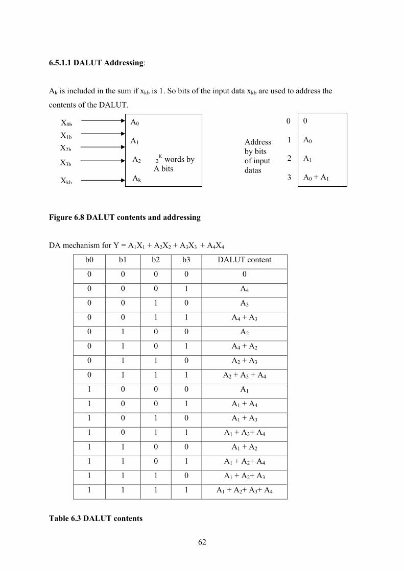
62
6.5.1.1 DALUT Addressing:
Ak is included in the sum if xkb is 1. So bits of the input data xkb are used to address the
contents of the DALUT.
Figure 6.8 DALUT contents and addressing
DA mechanism for Y = A1X1 + A2X2 + A3X3 + A4X4
b0 b1 b2 b3 DALUT content
0 0 0 0 0
0 0 0 1 A4
0 0 1 0 A3
0 0 1 1 A4 + A3
0 1 0 0 A2
0 1 0 1 A4 + A2
0 1 1 0 A2 + A3
0 1 1 1 A2 + A3 + A4
1 0 0 0 A1
1 0 0 1 A1 + A4
1 0 1 0 A1 + A3
1 0 1 1 A1 + A3+ A4
1 1 0 0 A1 + A2
1 1 0 1 A1 + A2+ A4
1 1 1 0 A1 + A2+ A3
1 1 1 1 A1 + A2+ A3+ A4
Table 6.3 DALUT contents
A0
A1 A2 2
K words by A bits
Ak
X0b
X1b X2b
X3b
Xkb
0 A0 A1 A0 + A1
0
1
2
3
Address by bits of input datas

63
6.5.1.2 The Speed Tradeoff The arithmetic operations have now been reduced to addition, subtraction, and binary scaling.
With scaling by negative or positive powers of 2, the actual implementation entails the
shifting of binary coded data words toward the least significant bit and the use of sign
extension bits to maintain the sign at its normal bit position. The hardware implementation of
a binary full adder (as is done in the CLBs) entails two operands, the addend and the augend
to produce sum and carry output bits. The multiple bit-parallel additions of the DALUT
outputs can only be performed with a single parallel adder if this adder is time-shared.
Alternatively, if simultaneous addition of all DALUT outputs is required, an array of parallel
adders is required. These opposite goals represent the classic speed-cost tradeoff.
For B =16 Eq.6.4 becomes
Y = -[sum0] + [sum1] 2-1 + ………………. +[sum15]2-15
By successively decomposing in to two input adders the following figure can be obtained.
Figure 6.9 Fully parallel DA model with k =16 and B = 16
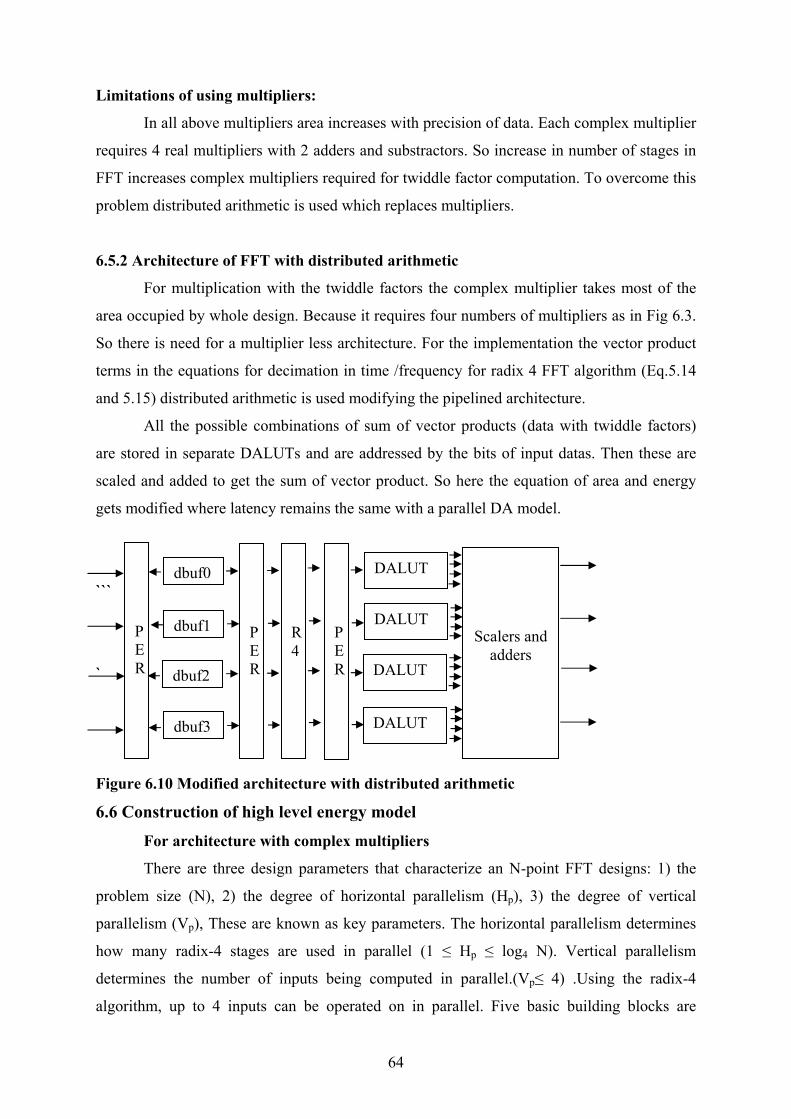
64
Limitations of using multipliers:
In all above multipliers area increases with precision of data. Each complex multiplier
requires 4 real multipliers with 2 adders and substractors. So increase in number of stages in
FFT increases complex multipliers required for twiddle factor computation. To overcome this
problem distributed arithmetic is used which replaces multipliers.
6.5.2 Architecture of FFT with distributed arithmetic
For multiplication with the twiddle factors the complex multiplier takes most of the
area occupied by whole design. Because it requires four numbers of multipliers as in Fig 6.3.
So there is need for a multiplier less architecture. For the implementation the vector product
terms in the equations for decimation in time /frequency for radix 4 FFT algorithm (Eq.5.14
and 5.15) distributed arithmetic is used modifying the pipelined architecture.
All the possible combinations of sum of vector products (data with twiddle factors)
are stored in separate DALUTs and are addressed by the bits of input datas. Then these are
scaled and added to get the sum of vector product. So here the equation of area and energy
gets modified where latency remains the same with a parallel DA model.
```
`
Figure 6.10 Modified architecture with distributed arithmetic
6.6 Construction of high level energy model
For architecture with complex multipliers
There are three design parameters that characterize an N-point FFT designs: 1) the
problem size (N), 2) the degree of horizontal parallelism (Hp), 3) the degree of vertical
parallelism (Vp), These are known as key parameters. The horizontal parallelism determines
how many radix-4 stages are used in parallel (1 ≤ Hp ≤ log4 N). Vertical parallelism
determines the number of inputs being computed in parallel.(Vp≤ 4) .Using the radix-4
algorithm, up to 4 inputs can be operated on in parallel. Five basic building blocks are
P E R
P E R
R 4
dbuf0
dbuf1
dbuf3
dbuf2
PER
DALUT
DALUT
DALUT
DALUT
Scalers and adders

65
considered affecting the architecture. They are radix-4 butterfly, data buffer, data path
permutation, parallel-to-serial/serial-to-parallel Mux, and twiddle factor computation.
For modified architecture with distributed arithmetic
There are four design parameters that characterize an N-point FFT designs: 1) the
problem size (N), 2) the degree of horizontal parallelism (Hp), 3) the degree of vertical
parallelism (Vp), 3) Number of stages (KP = log4N).These are known as key parameters. The
horizontal parallelism determines how many radix-4 stages are used in parallel (1 ≤ Hp ≤ KP).
Vertical parallelism determines the number of inputs being computed in parallel.(Vp≤ 4)
.Using the radix-4 algorithm, up to 4 inputs can be operated on in parallel. Seven basic
building blocks are considered affecting the architecture. They are radix-4 butterfly, data
buffer, data path permutation, parallel-to-serial/serial-to-parallel Mux, twiddle factor
computation , distributed arithmetic look up table(DALUT) and scalar-adder unit(SCA) as
Fig. 6.9).
6.6.1 Generation of energy, area and latency functions
For architecture with complex multipliers
In FPGA designs with streams of data, throughput is an important factor in
energy dissipation. Thus, in the pipelined design, the energy equation is E = P/Th, where P is
the average power dissipation and Th is the throughput of the design. Note that 1/Th = L can
be considered the effective latency of the design. The effective latency accounts for the
benefits of overlapping computations in pipelining. Based on the architecture and algorithm,
it can be shown that the equation to calculate the latency (L), of computing an N-point, radix-
4 FFT is:
L = N log4 N / (Vp × Hp)
Where L is in cycles. To convert this latency to seconds, it is divided by the clock frequency.
Also the types of FPGA components (multipliers, registers, etc.) and the amounts of each
type of component that are used by for five basic building blocks are known. The power
function for each basic building block is obtained using the techniques in [Ch 1]. The average
power dissipation of each block is summed to estimate the total power dissipation. Since
power is energy divided by latency, and the latency is calculated earlier, the power is
multiplied by the latency to estimate the energy used in executing the algorithm. The power
functions for the data buffer, the radix-4 block, the data path permutation, parallel-to-

66
serial/serial-to-parallel Mux, and the twiddle computation block are PDB, PR4, PPER, PPS/SP and
PTW, respectively,
E = L {VP (HP+1)PDB + 2m HP PPER + (HP)PR4 +2s(HP-1) PPS/SP + tvth PTW + 2VPPIO
Where the key parameters are VP and HP and the components are Radix 4 Butterfly
(R4), Data Buffer (Dbuf), Permutation unit (PER), Mux(PS/SP) and I/Os. Here m is the
number of the data path permutation block (m = 1 when Vp = 4, otherwise m = 0), s is the
number of parallel to- serial/serial-to-parallel muxes (s = 1 when Hp = 1, otherwise s = 0). tv th
is the number of twiddle computation blocks (tv = Vp−1 when Vp = 4, otherwise tv = Vp; th =
Hp−1 when Hp = log4 N, otherwise th = Hp).
For modified architecture with distributed arithmetic
Latency L = N log4 N / (Vp × Hp)
To keep latency unaltered a fully parallel model of DA is used as Fig.6.9.First stage of
butterfly R4 is kept as it does not require twiddle factor multiplication. Then parallel
DALUTs are addressed by the bits of intermidiate datas in parallel. N datas got from the
LUTs are given to the scaler-adder unit(SCA) .SCA consist of N/2 adders(N/4 scalers) in
first stage, N/4 adders(N/8 scalers) in the second stage, N/8 adders(N/16 scalers) in the third
stage and so on until one adder is there to generate final product.
Energy E = L{VPHPPDB + HPPR4 + 2(N/4)PDALUT(KP - HP) + 2VP(KP - HP)PSCA +
2VPPIO}
Where N is the number of data points in FFT. All other parameters are described earlier.
6.7 Results and discussion
The curve fitting is used in MATLAB to generate power and area functions for the
designs. Each of the component is simulated individually and area \ power values obtained by
Varying the component specific parameters (precision (w) and no. of entries(x)).These values
are given to power function builder to generate area and power functions in terms of
component specific parameters.

67
6.7.1 Comparison of the designs at high level
With complex multiplier
With Distributed arithmetic
N =16
(VP=4,
HP= 2)
N = 64
(VP=4,
HP= 3)
N =256
(VP=1,
HP= 4)
N =16
(VP=4,
HP = 1)
N = 64
(VP=4,
HP = 1)
N =256
(VP=4,
HP = 2) Energy
nj 127 1179 4399 109 745 3126
Area
(slices) 4331 7619 3044
3123 5528 9111
Latency
(usecs) 0.04 0.16 0.64 0.04 0.16 0.64
EAT 0.022 1.43 8.56 0.013 0.65 18.22
Table 6.4 Comparison of results obtained from functions (at 100 MHz)
6.7.2 Estimation of error from low level simulation
With complex multiplier
(VP = 4, HP = 2)
With Distributed arithmetic
(VP = 4, HP = 1)
N = 16
estimated actual Error (%) estimated actual Error (%) Energy(nj) 127 139 9.4 109 122 10.6 Area(slices) 4331 5022 13 3123 3499 2.8 Latency
(usecs) 0.04 0.04 0 0.04 0.04 0
Table 6.5 Comparison of results with actual values and error estimation (at 100 MHz)
6.7.3 Conclusion
The results are compared between the architectures with complex multiplier and with
distributed arithmetic from the functions obtained at high level. It shows that the use of
distributed arithmetic reduces the energy and area by keeping latency fixed. Also the values
obtained from low level simulation are compared against values obtained from functions.
Parameters (energy, area and latency) can be optimized at high level as values from Table 6.4
and Table 6.5 shows that the error obtained is within 20% between estimated values at high
level and actual values obtained from low level. So this method can be accepted for
optimization of parameters at algorithm level.

Chapter 7
Conclusion

68
7.1 Co ntributions
The key contributions of this research are:
1. Optimization of parameters at high level: Matrix multiplication and Fast Fourier
Transform designs optimized at algorithm and architecture level by using energy
efficient modeling technique.
2. Design and synthesis of matrix multiplication algorithms include pipelining and
parallel processing to reduce latency and increase throughput. Reduction of area
and energy by use of word width decomposition technique to the algorithms.
3. Design and synthesis of Fast Fourier Transform algorithms include pipelining to
reduce latency and increase throughput. Design of multiplier less architecture and
simpler VLSI implementation by use of distributed arithmetic due to look up table
features of FPGA. 7.2 Further work
This section suggests following work can be done in future in this thesis..
1. Algorithms used for matrix multiplication and Fast Fourier Transform use
pipelining and parallel processing for trade off between various parameters. These
algorithms can further be modified to obtain different latencies against variation of
other key parameters.
2. Designs of matrix multiplication can be used in some practical applications like
software defined radio to verify performance against variation of different key
parameters.
3. Designs of Fast Fourier Transform can be used to verify its performance through a
spectrum analyzer.
4. This design can be modified at algorithm level to use high precision data formats.
7.2.1 Higher-Precision Data Formats
Modern digital processors represent data using notations that generally can be
classified as fixed-point, floating-point, or block-floating-point. These three data notations
vary in complexity, dynamic range, and resolution. The designed FFT processor uses a fixed-
point notation for data words. We now briefly review the other two data notations and
consider several issues related to implementing block-floating-point this work.
Background
Fixed-point In fixed-point notation, each datum is represented by a single signed or unsigned
(non-negative) word. The implemented FFT processor uses a signed, 2’s-complements, and
fixed-point data word format.

69
Floating-point In floating-point notation, each datum is represented by two components: a
mantissa and an exponent in the following configuration: mantissa x base exponent. The base
is fixed, and is typically two or four. Both the mantissa and exponent are generally signed
numbers. Floating-point formats provide greatly increased dynamic range, but significantly
complicate arithmetic units since normalization steps are required whenever data are
modified.
Block-floating-point Block-floating-point notation is probably the most popular format for
dedicated FFT processors and is similar to floating-point notation except that exponents are
shared among "blocks" of data. For FFT applications, a block of data is typically N words.
Using only one exponent per block dramatically reduces a processor's complexity since
words are normalized uniformly across all words within a block. The complexity of a block-
floating-point implementation is closer to that of a fixed-point implementation than that of a
floating-point one. However, in the worst case, block-floating-point performs the same as
fixed-point.
Convergent block floating point When a pipelined architecture is used, it is not efficient to
wait until stage N has finished determining the scaling factor. Instead a method called
Convergent Block Floating Point (CBFP). The basic idea is that the output from a radix-4
stage is a set of 4 independent groups that can use different scale factors. After the first stage
there will be 4 groups, after the second stage 16 groups and so on. This will converge towards
one exponent for each output sample from the FFT. The same scheme can be applied for a
radix-2 stage, generating 2 independent groups at each stage. If the initial butterfly is of
radix-2 type, most implementations omit the CBFP logic in the first stage due to the large
memory overhead.
Applications to the design
While the fixed-point format permits a simple and fast design, it also gives the least dynamic
range for its word length. Floating-point and block-floating-point formats provide more
dynamic range, but are more complex. The architectures can be modified to use these formats
of data and verify the performance both at high and low level by construction of energy
model.

70
REFERENCES:
[1] Choi S., Jang J.W., Prasanna V.K., “Energy- and Time-Efficient Matrix
Multiplication on FPGAs.” IEEE. Transaction on (VLSI) systems. Volume 13, No.1,
(NOVEMBER 2005).
[2] Choi S., Jang J.W., and Prasanna V.K., Mohanty S., “Domain-specific modeling for
rapid energy estimation of reconfigurable architectures.” J.Supercomputing. Volume 26,
No. 3, (Nov. 2003): p. 259–281.
[3] Hong, Park K., and Mun Jun- Hee “Design and Implementation of a High-Speed
Matrix Multiplier Based on Word-Width Decomposition.” IEEE. Transaction on(VLSI)
systems. Volume 14, No. 4, (APRIL 2006).
[4] Mencer O., Morf M.., and Flynn M. J., “PAM-Blox: High performance FPGA design
for adaptive computing.” Field-Programmable CustomComputing Machines (FCCM).
(1998): p. 167–174.
[5] Kung H. T., Leiserson C. E., “Systolic arrays for (VLSI).” Introduction to VLSI
Systems. (1980).
[6] Amira A., Bouridane A., Milligan P., “Accelerating matrix product on reconfigurable
hardware for signal processing.” Proc. 11th Int.Conf. Field-Programmable Logic and Its
Applications (FPL). (2001): p.101–111.
[7] Choi S., Jang J.W., and Prasanna V.K., “Energy efficient matrix multiplication on
FPGAs.” Proc. Field-Programmable Logic and Its Applications (FPL).(2002):p. 534–544.
[8] Kumar, Tsai Y., “On synthesizing optimal family of linear systolic arrays for matrix
multiplication.” IEEE Trans. Comput.. Volume 40, No. 6, (1991): p 770–774.
[9] Scrofano R., Jang J.W., PrasannaV.K., “Energy-Efficient discrete cosine transform on
FPGAs.” Proc. Engineering of ReconfigurableSystems and Algorithms (ERSA).(2003): p.
215–221.
[10] Shang L., Kaviani A., Bathala K., “Dynamic power consumption in Virtex-II FPGA
family.” Proc. Field-Programmable Gate Arrays(FPGA).(2002) : p. 157–164.
[11] Bass B., “A low-power, high-performance, 1024-point FFT processor.” IEEE J.
Solid-State Circuits. Volume 34, no. 3, (Mar. 1999): p. 380–387.
[12] Choi S., Govindu G., Jang J.W., Prasanna V.K., “Energy-efficient and
parameterized designs of fast fourier transforms on FPGAs.” Proc. Int. Conf. Acoustics,
Speech, and Signal Processing (ICASSP) Volume. 2, (2003): p. 521–524.

71
[13] Lin R., “Bit-matrix decomposition and dynamic reconfiguration: Unified arithmetic
processor architecture, design, and test.” Proc. ReconfigurableArch. Workshop (RAW).
(2002): p. 83.
[14] Lin R., “A reconfigurable low-power high-performance matrix multiplier
architecture with borrow parallel counters.” Proc. Reconfigurable Arch. Workshop
(RAW). (2003): p. 182.
[15] Lin R., “Reconfigurable parallel inner product processor architectures.” IEEE Trans.
Very Large Scale Integr. (VLSI) Syst.. Volume. 9, no. 2, (Apr. 2001): p.261–272.
[16] http://www.xilinx.com/univ/ML310/ml310_mainpage: ML310 Virtex-II Pro
Development Platform (Online).
[17] http://milan.usc.edu: Model-Based Integrated Simulation (Online)
[18] http://www.xilinx.com: Virtex-II Series and Xilinx ISE 7.1i Design Environment
(2001), Xilinx Application Note (Online).
[19] Brown, Yates C. I., “VLSI architecture for sparse matrix multiplication.”Electron.
Lett. Volume 32, No. 10, (May 1996):p. 891–893.
[20] Choi S., Jang J.W., Prasanna V.K., “Area and time efficient implementations of
matrix multiplication on FPGAs.” Proc. IEEE Int.Conf. Field Programmable Technol.
(2002): p. 93–100.
[21] Rabaey J. M., Chandrakasan A., Nikolic B. Digital Integrated Circuits:A Design
Persepective. Englewood Cliffs: Prentice-Hall, 2003.
[22] Baugh C. R. and Wooley, “A two’s complement parallel array multiplication
algorithm.” IEEE Trans. Comput. Volume C-22, No.1–2, (Jan. 1973): p. 1045–1047.
[23] Dick, “The Platform FPGA: Enabling the Software Radio.” Software Defined Radio
Technical Conferenceand Product Exposition (SDR). (November 2002)
[24] Oppenheim A.V. and Schafer R.W. Discrete-Time Signal Processing. Prentice Hall,
1989.
[25] Raghunathan A., Jha N. K., Dey, High-level Power Analysis and Optimization.
Kluwer Academic Publishers. 1998.
[26] Shang L., Kaviani, Bathala, “Dynamic Power Consumption in Virtex-II FPGA
Family.” International Symposium on Field Programmable GateArrays. (2002).
[27] Yeap G. Practical Low Power Digital VLSI Design,Kluwer. Academic Publishers,
1998.
[28] http://milan. usc.edu :Model-Based Integrated Simulation (Online)

72
[29] Choi S., Govindu G., Jang J.W., Prasanna V.K., “Energy-efficient and
parameterized designs of fast fourier transforms on FPGAs.” Proc. Int. Conf. acoustics,
Speech, and Signal Processing (ICASSP), Volume 2,(2003):p.521-524.
[30] Jia L. ,Gao Y. ,Isoaho J ,Tenhunen H. ,”A new VLSI orieneted FFT algorithm and
implementation.”IEEE(1998).
[31] Cormen T.H, .Leiserson C.E., Rivest R.L. Introduction to algorithms. Prentice-Hall,
1998.
[32] Bass B., “A Low-Power, High-Performance, 1024-Point FFT Processor.” IEEE
Journal of Solid-State Circuits.Volume. 34, No. 3 ,(1999): p.380-38.
[33] Cooley J. W., and Tukey J. W., “An Algorithmm for the Machine Computation of
Complex Fourier Series.” Mathematics of Computation. Volume.19, (Apr. 1965): p.297-
301.
[34] Despain A.M., “Very Fast Fourier Transform Algorithms Hardware for
Implementation”, IEEE Trans. on Computers, vol. c-28, no. 5, (May 1979).
[35] Swartzlander, Young, and Joseph, “A radix-4 delay commutater for fast Fourier
transform processor implementation.”
[36] Bernard, Krammer, Sauer, Schweizer R., “A pipeline architecture for modified
higher radix FFT.” IEEE International Conference on Acoustics, Speech, and Signal
Volume.5, (1992):p. 617-620.
[37] Cohen D., “Simplified control of FFT hardware.” IEEE Trans.Acoustics, Speech,
signal Processing, Volume. ASSP-24,(1976): p. 517-579
[38] Ma Y. T. “An effective memorv addressing scheme for FFT processors.” IEEE
trans.on signal processing, Volume 47, No. 3,( 1999) p.907-91 I .
[39] Perry D.L. ,VHDL Programming by Example. TATA McGraw-HILL, 2002