Embed Size (px)
Citation preview
Energy-dependent contrast in atomic-scale spin-polarized scanning tunneling microscopyof Mn3N2 (010): Experiment and first-principles theory
Rong Yang,* Haiqiang Yang, and Arthur R. Smith†
Nanoscale and Quantum Phenomena Institute, Department of Physics and Astronomy, Ohio University, Athens, Ohio 45701, USA
Alexey Dick and Jörg NeugebauerMax-Planck-Institut für Eisenforschung GmbH, Max-Planck Strasse 1, 40237 Düsseldorf, Germany
and Theoretische Physik, Universität Paderborn, Warburger Strasse 100, 33098 Paderborn, Germany�Received 7 May 2005; revised manuscript received 13 July 2006; published 21 September 2006�
The row-wise antiferromagnetic Mn3N2 �010� surface has been investigated using atomic-scale spin-polarized scanning tunneling microscopy. Localizing the experimental image at a particular region of thesurface, the bias voltage-dependent behavior and resulting energy-dependent magnetic contrast are investi-gated. It is found that the magnetic contrast varies strongly over the energy range from EFermi−1 eV toEFermi+1 eV, including a magnetic contrast reversal at �EFermi+0.4 eV. Spin-polarized density-functionaltheory has been combined with the spin-generalized Tersoff-Hamann model to simulate the experimentalresults on Mn3N2 �010�. Excellent agreement is found which shows that the observed bias-dependent behaviorderives from the properties of the sample surface, not the tunneling tip. The bias-dependent contrast reversal,as well as bias-dependent line profile shape, are both found to result from a transition from majority �dz2� tominority �dyz� spin-polarized Mn atomic orbital lobes.
DOI: 10.1103/PhysRevB.74.115409 PACS number�s�: 68.37.Ef, 75.70.�i, 75.50.Ee, 75.70.Rf
I. INTRODUCTION
Nanoscale magnetism is a topic of increasing interest,having potential applications in advanced data storage andspin-based electronics. One of the most powerful techniqueswith the ability to probe magnetic structure at the nanoscaleis spin-polarized scanning tunneling microscopy �SP-STM�.This technique offers spin sensitivity combined with thewell-known advantage of STM, namely, spatial resolutiondown to the atomic-scale. SP-STM has thus far been utilizedto great advantage in imaging both ferromagnetic andantiferromagnetic surface structures.1–11
The principle of SP-STM is based on the variation of thetunneling current with the angle between the spin of the tipand that of the sample—larger current for parallel orientationand smaller current for antiparallel orientation. This effectdepends on the local density of states for spin-↑ and spin-↓channels. SP-STM has been used by Wiesendanger et al. tomap the energy-dependent spin polarization of nanoscale fer-romagnetic Gd�0001� islands by applying a magnetic field tothe sample and measuring dI /dV versus V in the tip-sampleparallel and antiparallel configurations.2 For deriving the po-larization in the case of an antiferromagnetic �AFM� surface,an external field is not required since the parallel and anti-parallel configurations occur periodically as one moves thetip from row to row.
Regarding AFM surfaces, Heinze et al. reported theatomic-scale magnetic contrast of a Mn monolayer on aW�110� using atomic-scale SP-STM in constant current �CC�mode.4 Two years later, Yang et al. showed the simultaneousmagnetic and nonmagnetic contrast on Mn3N2 �010� usingalso atomic-scale SP-STM in CC mode.5 Very recently, Ku-betzka et al. have applied the same technique to study asingle monolayer of Fe on W�001�, resolving a long-standingquestion regarding the magnetic ground state of this
system.11 Atomic-scale SP-STM has therefore been estab-lished as a powerful technique for resolving the ultimatelimits of magnetic structure on surfaces.
In this paper, we explore the effect of bias voltage on themagnetic corrugation on AFM Mn3N2 �010�. The Mn3N2�010� surface is a model AFM surface for such studies. TheMn atoms of the highly bulklike surface have magnetic mo-ments that alternate in a row-wise AFM arrangement.10,12
Bulk measurements show the corresponding layer-wise AFMstructure with magnetic moments of Mn1 and Mn2, which areeach close to �3.5�B,13,14 and bulk theoretical calculationsare in good agreement.15 SP-STM corrugation profiles ingeneral are found to contain both magnetic and nonmagneticinformation. Here, it is found that the magnetic STM imagedepends strongly on the bias voltage, and at certain voltagethe magnetic amplitude goes to zero. The bias voltage depen-dence is also found to affect the SP-STM line profile shape.Comparisons of the experimental SP-STM images and heightprofiles to simulated SP-STM images and height profiles cal-culated from spin-polarized first-principles density-functional theory are shown. Straightforward interpretationof the obtained results with emphasis on the magnetic con-tribution is made, based on the electronic properties of theMn3N2 �010� surface.
II. EXPERIMENTAL APPROACH
The experiments are performed in a combined ultrahigh-vacuum �UHV� growth-analysis system that allows directUHV transfer of samples from the growth chamber to theSTM chamber. The MBE system includes a solid source ef-fusion cell for Mn and a rf plasma source for N. After beingheated up to 1000 °C for 30 min with the nitrogen plasmaturned on, the MgO substrate temperature is lowered to450 °C prior to the growth of manganese nitride
PHYSICAL REVIEW B 74, 115409 �2006�
1098-0121/2006/74�11�/115409�8� ©2006 The American Physical Society115409-1
Mn3N2�010� thin film. The nitrogen flow rate is about1.1 sccm �growth chamber pressure is 1.1�10−5 Torr� withthe rf power set at 500 W. The Mn flux is about 3.5�1014/cm2 s. The growth condition is monitored using re-flection high-energy electron diffraction �RHEED�.14 Follow-ing growth, the samples are investigated with in situ SP-STM. For normal STM studies, we use electrochemicallyetched tungsten tips that are cleaned in the ultrahigh-vacuumchamber using electron bombardment. For SP-STM studies,we coat the cleaned tips with Fe at room temperature to athickness of 5–10 monolayers �ML�. Coated tips are magne-tized in a small �40 mT magnetic field directed perpendicu-lar to the tip axis. SP-STM images are taken in the constantcurrent �CC� mode at room temperature.
III. THEORETICAL APPROACH
In order to understand theoretically the magnetic surfacestructure of Mn3N2 �010�, we have performed an ab initiostudy. To describe the SP-STM experiments, we have usedthe spin-polarized Tersoff-Hamann approach. The tunnelingcurrent can be expressed as16
It �� dEgv�E��nt�E − eVbias�ns��Rt�,E�
+ mt�E − eVbias� · ms��Rt�,E�� . �1�
Here, gv�E�= f�E−EF�− f�E−EF−eVbias�, f is the Fermifunction, EF is the Fermi energy of the sample, and nt�E�,mt�E�, ns��Rt� ,E�, ms��Rt� ,E� are energy-dependent non-magnetic and magnetic densities of states �DOS� of the tipand local densities of states �LDOS� of the sample at the tipposition Rt, respectively. Since the exact geometric, elec-tronic, and magnetic properties of the tip used in the experi-ment are not known �and can even change during the experi-ment�, the conventional approach is to assume a tip with anenergy-independent DOS. Equation �1� can then be writtenas
It �� dEgv�E��ns��Rt�,E� + Ptms��Rt�,E�� . �2�
Here, ms��Rt� ,E�= ms��Rt� ,E� and −1.0� Pt�1.0 is the ef-fective spin polarization of the tip. gv�E� has been calculatedwith thermal smearing kBT=0.025 eV, which corresponds toexperimental conditions.
The nonmagnetic ns��Rt� ,E� and magnetic ms��Rt� ,E�LDOS of the sample entering Eq. �2� have been calculatedemploying density-functional theory. Ab initio based multi-scale library S/PHI/nX �Ref. 17� has been used for analysisof the calculated data and for simulation of the SP-STMprofiles. To get accurate surface geometry and electronicstructure, we have used a plane-wave norm-conservingpseudopotential approach as implemented in ABINIT.18,19 Mnand N have been represented by Troullier-Martins pseudopo-tentials with 3d, 4s, 4p �Mn� and 2s, 2p �N� states as va-lence. Nonlinear core correction has been included into theMn pseudopotential. A plane-wave energy cutoff of 50 Ryand a 3�1�1�3�1�3� Monkhorst-Pack mesh for slab
�bulk� have been found to give converged results with re-spect to bulk geometry and surface energies. The bulk geom-etry has been calculated fully accounting for internal relax-ations of the atomic structure. To ensure convergence of theSP-STM corrugation maps with respect to the k-pointsampling, the 12�4�1 Monkhorst-Pack mesh has beenused.
To estimate the importance of the exchange-correlationfunctionals, we have performed two series of calculationsemploying either the spin-LDA20,21 or the spin-PBEapproximations,22 and cross-checked obtained data. We havefound that both functionals provide qualitatively similar SP-STM profiles, with magnetic contrast reversal occurring atpositive bias voltages. The lattice parameters and internalatomic coordinates calculated within the spin-PBE approxi-mation are, however, in a better agreement with experiment14
than that obtained within the spin-LDA functional �+1.5%and 1% for spin-PBE versus −2.5% and 7% for spin-LDA,respectively�. In the rest of the paper, therefore, we restrictthe discussion to results obtained within the spin-PBEexchange-correlation approximation.
The surface has been modeled by a repeated slab geom-etry with a slab thickness of six atomic layers. The surfaceunit cell is that of the magnetic structure, i.e, each layercontains six Mn and four N atoms. The surface geometry hasbeen kept unrelaxed, since forces acting onto atoms in thetopmost layer along the surface normal are found to be lessthan 5�10−3 H/Bohr. The slabs have been separated by avacuum region of 12 Å. Convergence checks showed thechosen slab and vacuum thickness to give error bars in thesurface energy of less then 0.5 meV/Å2, and to be well con-verged with respect to simulated SP-STM corrugationprofiles.
It is well known10,23 that due to exponential decay of thewave functions into the vacuum, the reliable description ofthe surface LDOS at tip-surface separations exceeding �3 Åis hardly feasible within the plane-wave basis set. To over-come this deficiency, we have employed the real-space ap-proach to describe the vacuum region. The real-space ap-proach is exact and is based on the projection of the wavefunctions from the plane-wave basis onto the real-spacebasis. The real-space basis functions are ideally suited todescribe the vacuum region since they include the exponen-tial decay of the wave functions with respect to the correcteffective vacuum potential, and provide exact descriptionof the surface LDOS at any tip-surface separation. The de-tailed description of the real-space method is givenelsewhere.23 In the case of the Mn3N2�010� surface, the real-space basis is used at tip-surface distances larger than 2.5 Å;the plane-wave basis is used everywhere else.
All STM simulations have been performed with a bias-independent constant tunneling current It�eVbias�= Iconst, tomodel the experimental constant current regime.
IV. RESULTS AND DISCUSSION
A. Magnetic contrast on Mn3N2 (010)
Previous work has elucidated the geometrical structureof the �010� surface, which is depicted in Fig. 1�a� in the top
YANG et al. PHYSICAL REVIEW B 74, 115409 �2006�
115409-2
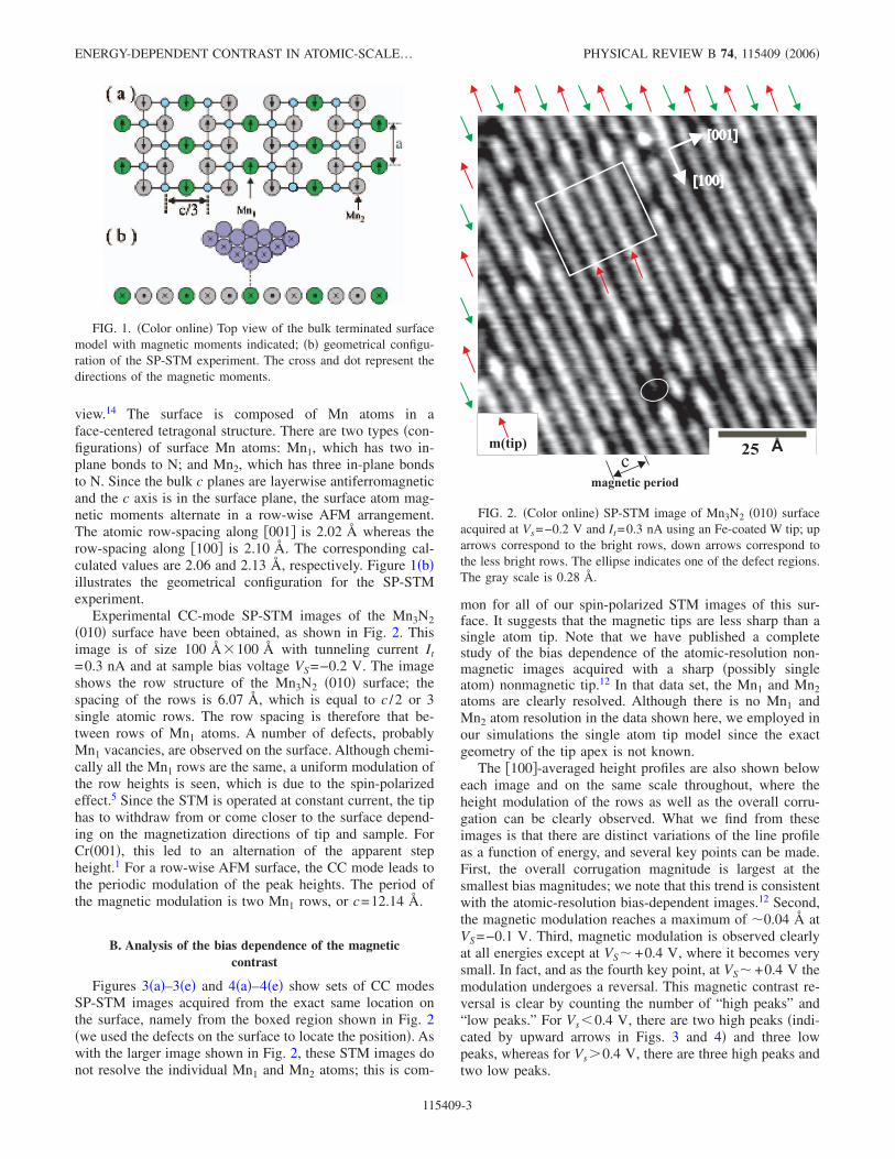
view.14 The surface is composed of Mn atoms in aface-centered tetragonal structure. There are two types �con-figurations� of surface Mn atoms: Mn1, which has two in-plane bonds to N; and Mn2, which has three in-plane bondsto N. Since the bulk c planes are layerwise antiferromagneticand the c axis is in the surface plane, the surface atom mag-netic moments alternate in a row-wise AFM arrangement.The atomic row-spacing along �001� is 2.02 Å whereas therow-spacing along �100� is 2.10 Å. The corresponding cal-culated values are 2.06 and 2.13 Å, respectively. Figure 1�b�illustrates the geometrical configuration for the SP-STMexperiment.
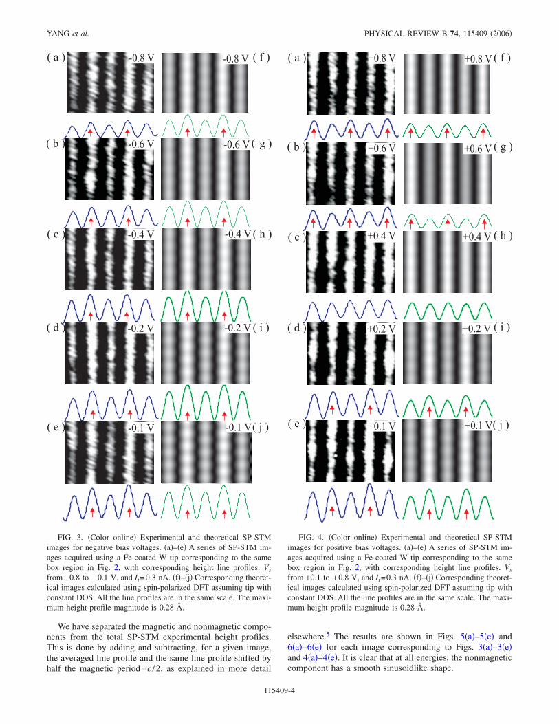
Experimental CC-mode SP-STM images of the Mn3N2�010� surface have been obtained, as shown in Fig. 2. Thisimage is of size 100 Å�100 Å with tunneling current It=0.3 nA and at sample bias voltage VS=−0.2 V. The imageshows the row structure of the Mn3N2 �010� surface; thespacing of the rows is 6.07 Å, which is equal to c /2 or 3single atomic rows. The row spacing is therefore that be-tween rows of Mn1 atoms. A number of defects, probablyMn1 vacancies, are observed on the surface. Although chemi-cally all the Mn1 rows are the same, a uniform modulation ofthe row heights is seen, which is due to the spin-polarizedeffect.5 Since the STM is operated at constant current, the tiphas to withdraw from or come closer to the surface depend-ing on the magnetization directions of tip and sample. ForCr�001�, this led to an alternation of the apparent stepheight.1 For a row-wise AFM surface, the CC mode leads tothe periodic modulation of the peak heights. The period ofthe magnetic modulation is two Mn1 rows, or c=12.14 Å.
B. Analysis of the bias dependence of the magneticcontrast
Figures 3�a�–3�e� and 4�a�–4�e� show sets of CC modesSP-STM images acquired from the exact same location onthe surface, namely from the boxed region shown in Fig. 2�we used the defects on the surface to locate the position�. Aswith the larger image shown in Fig. 2, these STM images donot resolve the individual Mn1 and Mn2 atoms; this is com-
mon for all of our spin-polarized STM images of this sur-face. It suggests that the magnetic tips are less sharp than asingle atom tip. Note that we have published a completestudy of the bias dependence of the atomic-resolution non-magnetic images acquired with a sharp �possibly singleatom� nonmagnetic tip.12 In that data set, the Mn1 and Mn2atoms are clearly resolved. Although there is no Mn1 andMn2 atom resolution in the data shown here, we employed inour simulations the single atom tip model since the exactgeometry of the tip apex is not known.
The �100�-averaged height profiles are also shown beloweach image and on the same scale throughout, where theheight modulation of the rows as well as the overall corru-gation can be clearly observed. What we find from theseimages is that there are distinct variations of the line profileas a function of energy, and several key points can be made.First, the overall corrugation magnitude is largest at thesmallest bias magnitudes; we note that this trend is consistentwith the atomic-resolution bias-dependent images.12 Second,the magnetic modulation reaches a maximum of �0.04 Å atVS=−0.1 V. Third, magnetic modulation is observed clearlyat all energies except at VS� +0.4 V, where it becomes verysmall. In fact, and as the fourth key point, at VS� +0.4 V themodulation undergoes a reversal. This magnetic contrast re-versal is clear by counting the number of “high peaks” and“low peaks.” For Vs�0.4 V, there are two high peaks �indi-cated by upward arrows in Figs. 3 and 4� and three lowpeaks, whereas for Vs�0.4 V, there are three high peaks andtwo low peaks.
FIG. 1. �Color online� Top view of the bulk terminated surfacemodel with magnetic moments indicated; �b� geometrical configu-ration of the SP-STM experiment. The cross and dot represent thedirections of the magnetic moments.
cmagnetic period
25 Å
[100][100]
[001][001]
m(tip)
FIG. 2. �Color online� SP-STM image of Mn3N2 �010� surfaceacquired at Vs=−0.2 V and It=0.3 nA using an Fe-coated W tip; uparrows correspond to the bright rows, down arrows correspond tothe less bright rows. The ellipse indicates one of the defect regions.The gray scale is 0.28 Å.
ENERGY-DEPENDENT CONTRAST IN ATOMIC-SCALE¼ PHYSICAL REVIEW B 74, 115409 �2006�
115409-3
We have separated the magnetic and nonmagnetic compo-nents from the total SP-STM experimental height profiles.This is done by adding and subtracting, for a given image,the averaged line profile and the same line profile shifted byhalf the magnetic period=c /2, as explained in more detail
elsewhere.5 The results are shown in Figs. 5�a�–5�e� and6�a�–6�e� for each image corresponding to Figs. 3�a�–3�e�and 4�a�–4�e�. It is clear that at all energies, the nonmagneticcomponent has a smooth sinusoidlike shape.
FIG. 3. �Color online� Experimental and theoretical SP-STMimages for negative bias voltages. �a�–�e� A series of SP-STM im-ages acquired using a Fe-coated W tip corresponding to the samebox region in Fig. 2, with corresponding height line profiles. Vs
from −0.8 to −0.1 V, and It=0.3 nA. �f�–�j� Corresponding theoret-ical images calculated using spin-polarized DFT assuming tip withconstant DOS. All the line profiles are in the same scale. The maxi-mum height profile magnitude is 0.28 Å.
FIG. 4. �Color online� Experimental and theoretical SP-STMimages for positive bias voltages. �a�–�e� A series of SP-STM im-ages acquired using a Fe-coated W tip corresponding to the samebox region in Fig. 2, with corresponding height line profiles. Vs
from +0.1 to +0.8 V, and It=0.3 nA. �f�–�j� Corresponding theoret-ical images calculated using spin-polarized DFT assuming tip withconstant DOS. All the line profiles are in the same scale. The maxi-mum height profile magnitude is 0.28 Å.
YANG et al. PHYSICAL REVIEW B 74, 115409 �2006�
115409-4
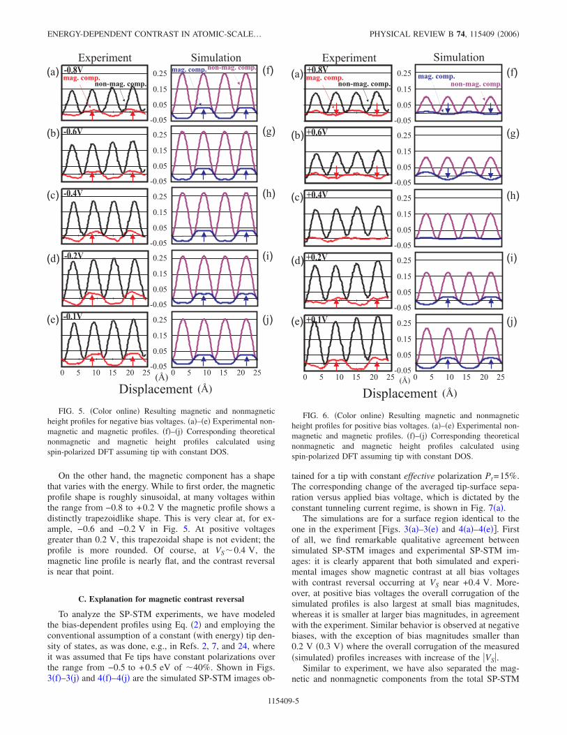
On the other hand, the magnetic component has a shapethat varies with the energy. While to first order, the magneticprofile shape is roughly sinusoidal, at many voltages withinthe range from −0.8 to +0.2 V the magnetic profile shows adistinctly trapezoidlike shape. This is very clear at, for ex-ample, −0.6 and −0.2 V in Fig. 5. At positive voltagesgreater than 0.2 V, this trapezoidal shape is not evident; theprofile is more rounded. Of course, at VS�0.4 V, themagnetic line profile is nearly flat, and the contrast reversalis near that point.
C. Explanation for magnetic contrast reversal
To analyze the SP-STM experiments, we have modeledthe bias-dependent profiles using Eq. �2� and employing theconventional assumption of a constant �with energy� tip den-sity of states, as was done, e.g., in Refs. 2, 7, and 24, whereit was assumed that Fe tips have constant polarizations overthe range from −0.5 to +0.5 eV of �40%. Shown in Figs.3�f�–3�j� and 4�f�–4�j� are the simulated SP-STM images ob-
tained for a tip with constant effective polarization Pt=15%.The corresponding change of the averaged tip-surface sepa-ration versus applied bias voltage, which is dictated by theconstant tunneling current regime, is shown in Fig. 7�a�.
The simulations are for a surface region identical to theone in the experiment �Figs. 3�a�–3�e� and 4�a�–4�e��. Firstof all, we find remarkable qualitative agreement betweensimulated SP-STM images and experimental SP-STM im-ages: it is clearly apparent that both simulated and experi-mental images show magnetic contrast at all bias voltageswith contrast reversal occurring at VS near +0.4 V. More-over, at positive bias voltages the overall corrugation of thesimulated profiles is also largest at small bias magnitudes,whereas it is smaller at larger bias magnitudes, in agreementwith the experiment. Similar behavior is observed at negativebiases, with the exception of bias magnitudes smaller than0.2 V �0.3 V� where the overall corrugation of the measured�simulated� profiles increases with increase of the VS.
Similar to experiment, we have also separated the mag-netic and nonmagnetic components from the total SP-STM
FIG. 5. �Color online� Resulting magnetic and nonmagneticheight profiles for negative bias voltages. �a�–�e� Experimental non-magnetic and magnetic profiles. �f�–�j� Corresponding theoreticalnonmagnetic and magnetic height profiles calculated usingspin-polarized DFT assuming tip with constant DOS.
FIG. 6. �Color online� Resulting magnetic and nonmagneticheight profiles for positive bias voltages. �a�–�e� Experimental non-magnetic and magnetic profiles. �f�–�j� Corresponding theoreticalnonmagnetic and magnetic height profiles calculated usingspin-polarized DFT assuming tip with constant DOS.
ENERGY-DEPENDENT CONTRAST IN ATOMIC-SCALE¼ PHYSICAL REVIEW B 74, 115409 �2006�
115409-5
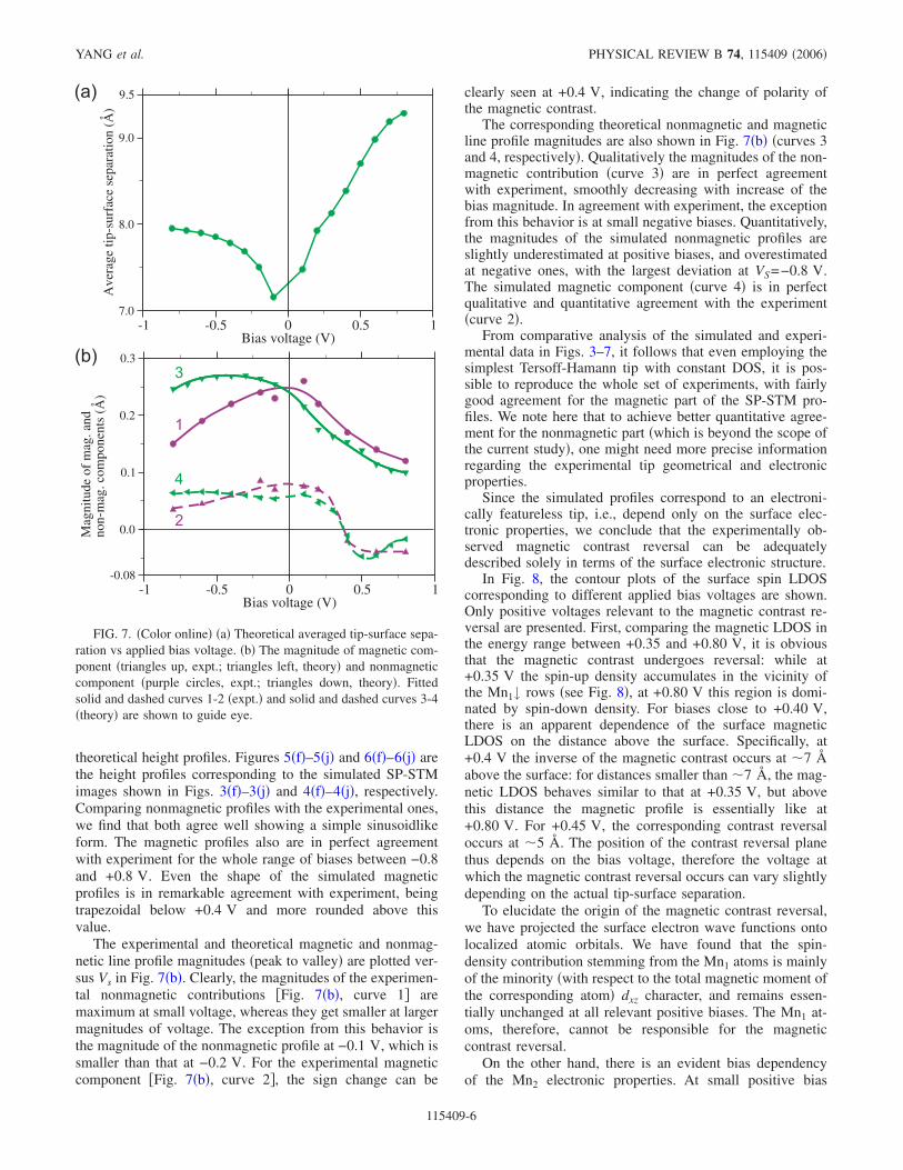
theoretical height profiles. Figures 5�f�–5�j� and 6�f�–6�j� arethe height profiles corresponding to the simulated SP-STMimages shown in Figs. 3�f�–3�j� and 4�f�–4�j�, respectively.Comparing nonmagnetic profiles with the experimental ones,we find that both agree well showing a simple sinusoidlikeform. The magnetic profiles also are in perfect agreementwith experiment for the whole range of biases between −0.8and +0.8 V. Even the shape of the simulated magneticprofiles is in remarkable agreement with experiment, beingtrapezoidal below +0.4 V and more rounded above thisvalue.
The experimental and theoretical magnetic and nonmag-netic line profile magnitudes �peak to valley� are plotted ver-sus Vs in Fig. 7�b�. Clearly, the magnitudes of the experimen-tal nonmagnetic contributions �Fig. 7�b�, curve 1� aremaximum at small voltage, whereas they get smaller at largermagnitudes of voltage. The exception from this behavior isthe magnitude of the nonmagnetic profile at −0.1 V, which issmaller than that at −0.2 V. For the experimental magneticcomponent �Fig. 7�b�, curve 2�, the sign change can be
clearly seen at +0.4 V, indicating the change of polarity ofthe magnetic contrast.
The corresponding theoretical nonmagnetic and magneticline profile magnitudes are also shown in Fig. 7�b� �curves 3and 4, respectively�. Qualitatively the magnitudes of the non-magnetic contribution �curve 3� are in perfect agreementwith experiment, smoothly decreasing with increase of thebias magnitude. In agreement with experiment, the exceptionfrom this behavior is at small negative biases. Quantitatively,the magnitudes of the simulated nonmagnetic profiles areslightly underestimated at positive biases, and overestimatedat negative ones, with the largest deviation at VS=−0.8 V.The simulated magnetic component �curve 4� is in perfectqualitative and quantitative agreement with the experiment�curve 2�.
From comparative analysis of the simulated and experi-mental data in Figs. 3–7, it follows that even employing thesimplest Tersoff-Hamann tip with constant DOS, it is pos-sible to reproduce the whole set of experiments, with fairlygood agreement for the magnetic part of the SP-STM pro-files. We note here that to achieve better quantitative agree-ment for the nonmagnetic part �which is beyond the scope ofthe current study�, one might need more precise informationregarding the experimental tip geometrical and electronicproperties.
Since the simulated profiles correspond to an electroni-cally featureless tip, i.e., depend only on the surface elec-tronic properties, we conclude that the experimentally ob-served magnetic contrast reversal can be adequatelydescribed solely in terms of the surface electronic structure.
In Fig. 8, the contour plots of the surface spin LDOScorresponding to different applied bias voltages are shown.Only positive voltages relevant to the magnetic contrast re-versal are presented. First, comparing the magnetic LDOS inthe energy range between +0.35 and +0.80 V, it is obviousthat the magnetic contrast undergoes reversal: while at+0.35 V the spin-up density accumulates in the vicinity ofthe Mn1↓ rows �see Fig. 8�, at +0.80 V this region is domi-nated by spin-down density. For biases close to +0.40 V,there is an apparent dependence of the surface magneticLDOS on the distance above the surface. Specifically, at+0.4 V the inverse of the magnetic contrast occurs at �7 Åabove the surface: for distances smaller than �7 Å, the mag-netic LDOS behaves similar to that at +0.35 V, but abovethis distance the magnetic profile is essentially like at+0.80 V. For +0.45 V, the corresponding contrast reversaloccurs at �5 Å. The position of the contrast reversal planethus depends on the bias voltage, therefore the voltage atwhich the magnetic contrast reversal occurs can vary slightlydepending on the actual tip-surface separation.
To elucidate the origin of the magnetic contrast reversal,we have projected the surface electron wave functions ontolocalized atomic orbitals. We have found that the spin-density contribution stemming from the Mn1 atoms is mainlyof the minority �with respect to the total magnetic moment ofthe corresponding atom� dxz character, and remains essen-tially unchanged at all relevant positive biases. The Mn1 at-oms, therefore, cannot be responsible for the magneticcontrast reversal.
On the other hand, there is an evident bias dependencyof the Mn2 electronic properties. At small positive bias
FIG. 7. �Color online� �a� Theoretical averaged tip-surface sepa-ration vs applied bias voltage. �b� The magnitude of magnetic com-ponent �triangles up, expt.; triangles left, theory� and nonmagneticcomponent �purple circles, expt.; triangles down, theory�. Fittedsolid and dashed curves 1-2 �expt.� and solid and dashed curves 3-4�theory� are shown to guide eye.
YANG et al. PHYSICAL REVIEW B 74, 115409 �2006�
115409-6
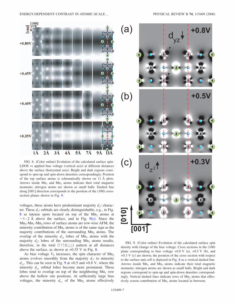
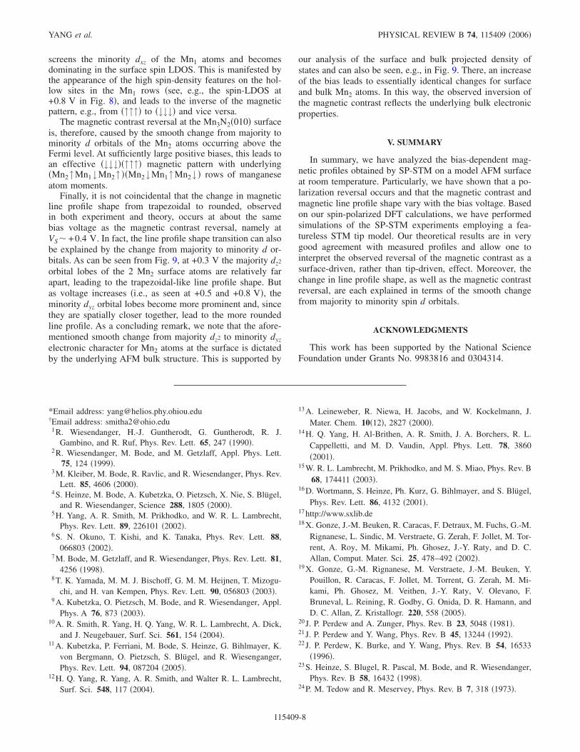
voltages, these atoms have predominant majority dz2 charac-ter. These dz2 orbitals are clearly distinguishable, e.g., in Fig.8 as intense spots located on top of the Mn2 atoms at�1–2 Å above the surface, and in Fig. 9�c�. Since theMn2-Mn1-Mn2 rows of surface atoms are row-wise AFM, theminority contribution of Mn1 atoms is of the same sign as themajority contributions of the surrounding Mn2 atoms. Theoverlap of the minority dxz lobes of Mn1 atoms with themajority dz2 lobes of the surrounding Mn2 atoms results,therefore, in the total �↑↑↑��↓↓↓� pattern at all distancesabove the surface, as shown at +0.35 V in Fig. 8.
As bias voltage VS increases, the spin character of Mn2atoms evolves smoothly from the majority dz2 to minoritydyz. This can be seen in Fig. 9 at +0.5 and +0.8 V, where theminority dyz orbital lobes become more prominent. Theselobes tend to overlap on top of the neighboring Mn1 rowabove the hollow site positions. At sufficiently large biasvoltages, the minority dyz of the Mn2 atoms effectively
FIG. 8. �Color online� Evolution of the calculated surface spin-LDOS vs applied bias voltage �vertical axis� at different distancesabove the surface �horizontal axis�. Bright and dark regions corre-spond to spin-up and spin-down densities correspondingly. Positionof the top surface atoms is schematically shown on 11 Å plots.Arrows inside Mn1 and Mn2 atoms indicate their total magneticmoments; nitrogen atoms are shown as small balls. Dashed linealong �001� direction corresponds to the position of the �100� cross-section planes shown in Fig. 9.
FIG. 9. �Color online� Evolution of the calculated surface spindensity with change of the bias voltage. Cross sections in the �100�plane corresponding to bias voltage +0.8 V �a�, +0.5 V �b�, and+0.3 V �c� are shown; the position of the cross section with respectto the surface unit cell is depicted in Fig. 8 as a vertical dashed line.Arrows inside Mn1 and Mn2 atoms indicate their total magneticmoments; nitrogen atoms are shown as small balls. Bright and darkregions correspond to spin-up and spin-down densities correspond-ingly. Vertical dashed lines indicate rows of Mn2 atoms that effec-tively screen contribution of Mn1 atoms located in between.
ENERGY-DEPENDENT CONTRAST IN ATOMIC-SCALE¼ PHYSICAL REVIEW B 74, 115409 �2006�
115409-7
screens the minority dxz of the Mn1 atoms and becomesdominating in the surface spin LDOS. This is manifested bythe appearance of the high spin-density features on the hol-low sites in the Mn1 rows �see, e.g., the spin-LDOS at+0.8 V in Fig. 8�, and leads to the inverse of the magneticpattern, e.g., from �↑↑↑� to �↓↓↓� and vice versa.
The magnetic contrast reversal at the Mn3N2�010� surfaceis, therefore, caused by the smooth change from majority tominority d orbitals of the Mn2 atoms occurring above theFermi level. At sufficiently large positive biases, this leads toan effective �↓↓↓��↑↑↑� magnetic pattern with underlying�Mn2↑Mn1↓Mn2↑ ��Mn2↓Mn1↑Mn2↓ � rows of manganeseatom moments.
Finally, it is not coincidental that the change in magneticline profile shape from trapezoidal to rounded, observedin both experiment and theory, occurs at about the samebias voltage as the magnetic contrast reversal, namely atVS� +0.4 V. In fact, the line profile shape transition can alsobe explained by the change from majority to minority d or-bitals. As can be seen from Fig. 9, at +0.3 V the majority dz2
orbital lobes of the 2 Mn2 surface atoms are relatively farapart, leading to the trapezoidal-like line profile shape. Butas voltage increases �i.e., as seen at +0.5 and +0.8 V�, theminority dyz orbital lobes become more prominent and, sincethey are spatially closer together, lead to the more roundedline profile. As a concluding remark, we note that the afore-mentioned smooth change from majority dz2 to minority dyzelectronic character for Mn2 atoms at the surface is dictatedby the underlying AFM bulk structure. This is supported by
our analysis of the surface and bulk projected density ofstates and can also be seen, e.g., in Fig. 9. There, an increaseof the bias leads to essentially identical changes for surfaceand bulk Mn2 atoms. In this way, the observed inversion ofthe magnetic contrast reflects the underlying bulk electronicproperties.
V. SUMMARY
In summary, we have analyzed the bias-dependent mag-netic profiles obtained by SP-STM on a model AFM surfaceat room temperature. Particularly, we have shown that a po-larization reversal occurs and that the magnetic contrast andmagnetic line profile shape vary with the bias voltage. Basedon our spin-polarized DFT calculations, we have performedsimulations of the SP-STM experiments employing a fea-tureless STM tip model. Our theoretical results are in verygood agreement with measured profiles and allow one tointerpret the observed reversal of the magnetic contrast as asurface-driven, rather than tip-driven, effect. Moreover, thechange in line profile shape, as well as the magnetic contrastreversal, are each explained in terms of the smooth changefrom majority to minority spin d orbitals.
ACKNOWLEDGMENTS
This work has been supported by the National ScienceFoundation under Grants No. 9983816 and 0304314.
*Email address: [email protected]†Email address: [email protected] R. Wiesendanger, H.-J. Guntherodt, G. Guntherodt, R. J.
Gambino, and R. Ruf, Phys. Rev. Lett. 65, 247 �1990�.2 R. Wiesendanger, M. Bode, and M. Getzlaff, Appl. Phys. Lett.
75, 124 �1999�.3 M. Kleiber, M. Bode, R. Ravlic, and R. Wiesendanger, Phys. Rev.
Lett. 85, 4606 �2000�.4 S. Heinze, M. Bode, A. Kubetzka, O. Pietzsch, X. Nie, S. Blügel,
and R. Wiesendanger, Science 288, 1805 �2000�.5 H. Yang, A. R. Smith, M. Prikhodko, and W. R. L. Lambrecht,
Phys. Rev. Lett. 89, 226101 �2002�.6 S. N. Okuno, T. Kishi, and K. Tanaka, Phys. Rev. Lett. 88,
066803 �2002�.7 M. Bode, M. Getzlaff, and R. Wiesendanger, Phys. Rev. Lett. 81,
4256 �1998�.8 T. K. Yamada, M. M. J. Bischoff, G. M. M. Heijnen, T. Mizogu-
chi, and H. van Kempen, Phys. Rev. Lett. 90, 056803 �2003�.9 A. Kubetzka, O. Pietzsch, M. Bode, and R. Wiesendanger, Appl.
Phys. A 76, 873 �2003�.10 A. R. Smith, R. Yang, H. Q. Yang, W. R. L. Lambrecht, A. Dick,
and J. Neugebauer, Surf. Sci. 561, 154 �2004�.11 A. Kubetzka, P. Ferriani, M. Bode, S. Heinze, G. Bihlmayer, K.
von Bergmann, O. Pietzsch, S. Blügel, and R. Wiesenganger,Phys. Rev. Lett. 94, 087204 �2005�.
12 H. Q. Yang, R. Yang, A. R. Smith, and Walter R. L. Lambrecht,Surf. Sci. 548, 117 �2004�.
13 A. Leineweber, R. Niewa, H. Jacobs, and W. Kockelmann, J.Mater. Chem. 10�12�, 2827 �2000�.
14 H. Q. Yang, H. Al-Brithen, A. R. Smith, J. A. Borchers, R. L.Cappelletti, and M. D. Vaudin, Appl. Phys. Lett. 78, 3860�2001�.
15 W. R. L. Lambrecht, M. Prikhodko, and M. S. Miao, Phys. Rev. B68, 174411 �2003�.
16 D. Wortmann, S. Heinze, Ph. Kurz, G. Bihlmayer, and S. Blügel,Phys. Rev. Lett. 86, 4132 �2001�.
17 http://www.sxlib.de18 X. Gonze, J.-M. Beuken, R. Caracas, F. Detraux, M. Fuchs, G.-M.
Rignanese, L. Sindic, M. Verstraete, G. Zerah, F. Jollet, M. Tor-rent, A. Roy, M. Mikami, Ph. Ghosez, J.-Y. Raty, and D. C.Allan, Comput. Mater. Sci. 25, 478–492 �2002�.
19 X. Gonze, G.-M. Rignanese, M. Verstraete, J.-M. Beuken, Y.Pouillon, R. Caracas, F. Jollet, M. Torrent, G. Zerah, M. Mi-kami, Ph. Ghosez, M. Veithen, J.-Y. Raty, V. Olevano, F.Bruneval, L. Reining, R. Godby, G. Onida, D. R. Hamann, andD. C. Allan, Z. Kristallogr. 220, 558 �2005�.
20 J. P. Perdew and A. Zunger, Phys. Rev. B 23, 5048 �1981�.21 J. P. Perdew and Y. Wang, Phys. Rev. B 45, 13244 �1992�.22 J. P. Perdew, K. Burke, and Y. Wang, Phys. Rev. B 54, 16533
�1996�.23 S. Heinze, S. Blugel, R. Pascal, M. Bode, and R. Wiesendanger,
Phys. Rev. B 58, 16432 �1998�.24 P. M. Tedow and R. Meservey, Phys. Rev. B 7, 318 �1973�.
YANG et al. PHYSICAL REVIEW B 74, 115409 �2006�
115409-8