Embed Size (px)
Citation preview

Energy management, wireless and
system solutions for highly integrated
implantable devices
Memòria presentada per
Jordi Parramon i Piella
per optar al grau de
Doctor en Enginyeria Electrònica

Departament d’Enginyeria Electrònica
Edifici Cn 08193 Bellaterra (Barcelona). Spain Tel.: 93 581 31 83 FAX: 93 581 13 50 E-mail: [email protected]
La Dra. Elena Valderrama Valles, Catedràtica d’Informàtica de la Universitat
Autònoma de Barcelona,
CERTIFICA
Que la memòria “Energy management, wireless and system solutions for
highly integrated implantable devices” que presenta Jordi Parramon i Piella per
optar al grau de Doctor en Enginyeria Electrònica, ha estat realitzat sota la seva
supervisió.
Bellaterra, Desembre del 2001
Dra. Elena Valderrama Valles

ii
ABSTRACT
In the recent years a very challenging product line of the biomedical industry has
emerged, with a fast-growing market and very promising future: implantable electronic
devices. Reliability, miniaturization and life-time are key problems of this business. New
technologies, especially microelectronics, are capable of giving answers to such
challenges.
The following thesis describes a variety of solutions developed in the framework
of several projects in terms of power management (with both RF and battery powered
approaches), high-bandwidth bi-directional wireless communication and system design
and architecture to be applied into highly integrated implantable devices.
RESUM
En els últims anys una nova línia de productes dins la indústria biomèdica a
començat a prendre embranzida, presentant un elevat creixement i unes perspectives de
futur molt encoratjadores: dispositius electrònics implantables. Els problemes més crítics
es troben en el fet que els implants han de ser molt segurs, de tamany reduït i han de tenir
un temps de vida llarg. Només les noves tecnologies, entre elles especialment la
microelectrònica, són capaces de donar resposta a aquests reptes.
La present tesi doctoral descriu una varietat de solucions desenvolupades en el
marc de diferents projectes enfocades a solucionar el problema del subministrament
d’energia (ja sigui usant camps electromagnètics o bateries), la comunicació d’alta
velocitat amb el món exterior i d’altres problemes a nivell de sistema, sempre en el marc
de dispositius electrònics altament integrables.

iii
AGRAïMENTS:
Des del dia en que com a estudiant no graduat vaig rebre la “proposición
indecente” en paraules textuals de l’Elena Valderrama per formar part del projecte
europeu INTER (i enllestir el meu projecte final de carrera d’Enginyeria Electrònica) fins
avui mateix que estic vivint a Califòrnia, m’han passat força coses tant a nivell
professional com personal. Entre altres aquesta tesi doctoral que és el resultat explícit de
la feina feta durant una sèrie d’anys sobretot al Centre Nacional de Microelectrònica, en
particular dins el grup d’aplicacions biomèdiques. Voldria expressar primer de tot el meu
agraïment a l’Elena, no només pel fet d’acceptar dirigir-me la tesi, sinó també pel
privilegi que suposa haver estat treballant al seu costat. Un altre motiu d’agraïment i que
comparteix amb el director del CNM Francesc Serra-Mestres es remunta a quan vaig
començar amb tot això de l’electrònica. Durant el primer curs, jo anava molt atrafegat
amb la simultaneïtat d’estudis amb Ciències Físiques. I més d’una vegada em vaig
plantejar deixar-ho. Van ser les seves classes en gran mesura les que van motivar-me a
continuar.
Vull també donar les gràcies a la Tere Osés, la Rosa Villa i en Jordi Aguiló del
CNM-GAB per creure i seguir creient que la microelectrònica i la biomedicina poden
tenir molt a veure. De l’UAB voldria donar les gràcies tant a la Núria Barniol com a en
Joan Oliver per haver–me ajudat valuosament als inicis del doctorat. Agraeixo tant a
David Marín que va continuar la feina de telemetria quan jo vaig marxar als Estats Units,
com a Pacu Serra-Graells, Ivan Erill, i en general a tots els companys del CNM per haver
compartit amb ells tantes hores.
De les meves dues estades i posterior col.laboració amb l’institut Fraunhoffer de
biomedicina IBMT de Sant Ingbert-Alemanya voldria agrair especialment a l’Uwe Meyer
per invitar-me cordiarlment al seu centre. També un agraïment per Oliver Scholz,
Hasnsjoerg Beutel i altres companys de centre amb qui vaig poder compartir treball i
amistat.

iv
De la meva estada d’un any als Estats Units a cavall entre la Case Western
Reserve University i la The University of Memphis, voldria agrair especialment el
mentoratge del professor Michael R. Neuman, aixi com poder haver treballat amb B.D.
Pendley i rebut ajuda de l’estudiant Chat Rowan.
Del projecte ITUBR vull agrair a tots els centres integrants l’esforç que van
realitzar i que en gran mesura ha fet possible aquesta tesi doctoral. En particular pel que
fa referència al desenvolupament de la unitat externa de telemetria i packaging voldria
agrair el treball de Julio Arzuaga i demés membres del CCC d’Uruguay. També cal
agrair tant a la Universidad de Los Andes amb el professor Antonio García-Rozo com a
la Fundación Cardio-infantil de Bogotà amb el professor Juan Carlos Briceño per haver
col.laborat decisivament en l’obtenció de resultats in-vivo. Però per sobre de tot una cosa
he d’agrair al Professor García-Rozo: el fet d’haver-se posat malalt dies abans de
celebrar-se una reunió del projecte ITUBR a Mèxic DF. Per estranyes circumstàncies de
la vida aquest fet va fer possible conèixer la Isabel que ara és la meva dona. De qui per
cert he d’agrair (o mes aviat lamentar) les seves despiatades correccions a la meva pobra
gramàtica anglesa.
Cal també donar gràcies a la Generalitat de Catalunya per haver-me pagat el sou
mitjantcant una beca pre-doctoral FPI durant els anys de doctorat i també pel fet d’ajudar-
me incondicionalment a obtenir del govern espanyol una carta de “no objecció” per tal
que pogués incorporar-me a una companyia de Califòrnia sense haver d’estar els pre-
establerts dos anys a Espanya per poder canviar el meu estatus de visat.
De la companyia Advanced Bionics Corporation, on continuo podent gaudir de la
recerca en micro-dispositius electrònics implantables voldria agrair especialment la
insistència del meu director Matt Haller, per tal que acabes d’escriure la tesi.
Ja per enllestir, voldria donar les gràcies a l’Amàlia, a tots els meus amics, i a tots
els membres de la meva família, en particular als meus pares.

v
ACKNOWLEDGEMENTS:
Since the day I received, as an undergraduate student, the proposal from Elena
Valderrama to join the European INTER project (and finish my EE final project) until
today that I am living in California, many things have happened to me in both the
personal and professional level. Among them the following doctoral thesis, that is the
result of the work done mainly in the CNM-, in particular in the biomedical applications
group. I would like first of all, to thanks Elena, not only because she accepted me as a
PhD student but also because it was truly a pleasure to work with her. Another reason
that I must acknowledge from her, in that case shared with the director of the CNM
Francesc Serra-Mestres, is related with the beginning of my studies in engineering.
During the first year, I was really busy trying to keep up with the EE at the same time
than with Physics. And more than once I had second thoughts about just giving up. Their
teaching help me a lot to keep going.
I would like to thanks Tere Oses, Rosa Villa and Jordi Aguilo, from CNM-GAB
to believe that microelectronics and biomedical applications may have quite a future
together. From the UAB I thank Nuria Barniol and Joan Oliver because they were the
first to help me valuably in the beginning of my work. I also acknowledge David Marin
to continue the work I did, right after my departure to the States, as well as Pacu Serra-
Graells, Ivan Erill and in general all the friends and colleagues of the CNM.
From my two visits to the Fraunhoffer institute of biomedicine IBMT-Germany, I
would like to thanks Uwe Meyer to be so kind to accept me there. As well as Oliver
Scholz, Hansjoerg Beutel and other colleagues from whom I was able to share work and
friendshipness.
During my thesis, I spend one year in the US working as a research visitor at Case
Western Reserve University and at The University of Memphis. All this was possible
thanks to professor Mike R. Neuman who kindly accept me in his group. I also appreciate

vi
the possibility to work with B.D. Pendley and with the undergraduate student Char
Rowan that helped me valuably.
From the ITUBR project I would like to thank every single center involved in the
effort that made possible this thesis. In particular related of the external controller
development I thank Julio Arzuaga and the rest of the people from CCC of Uruguay. I
also thank the Universidad de Los Andes with professor Antonio Garcia-Rozo and the
Fundacion Cardio Infantil with professor Juan Carlos Bricenno of Colombia whose help
was decisive in order to obtain in-vivo results. But above all, I thank professor Garcia-
Rozo for one thing: the fact he got ill a few days before a meeting project was about to
start in Mexico City. This made possible to meet Isabel who is now my wife. And of
which I have to thank (or maybe regret) her merciless correction to my poor English
grammar.
I would like to thank the Catalan government who sponsored my PhD through a
full time grant with the FPI program, and also because it helped me unconditionally to
obtain from the Spanish government a “no-objection” letter, that allowed me to join a US
company without having to wait the required two years in Spain, due to my immigration
visa issues.
I also thank Advanced Bionics Corporation, where I continue to have the pleasure
to work with implantable micro-systems and specially Matt Haller, due to his constant
insistence in reminding me that I should finish the thesis.
I finally thank to Amalia, to all my friends and my family, and especially my
parents.

vii
TABLE OF CONTENTS
CHAPTER ONE__________________________________________________ 1
INTRODUCTION______________________________________________ 1
1.1 Overview of implantable electronic devices ______________________ 1
1.2 Scope and Structure of the thesis ______________________________ 5
1.3 References ________________________________________________ 7
CHAPTER TWO ________________________________________________ 11
TRANSCUTANEOUS POWER TRANSMISSION _________________ 11
2.1 Introduction ______________________________________________ 11
2.2 Electromagnetic compatibility _______________________________ 13
2.3 Inductive link_____________________________________________ 19
2.3.1 Basic concepts ________________________________________ 19
2.3.2 Mutual inductance studies _______________________________ 20
2.3.3 Coil development ______________________________________ 23
2.3.4 Very-low coupling analytical study ________________________ 25
2.4 Internal power receiver _____________________________________ 29
2.4.1 Integration ___________________________________________ 30
2.4.2 Results ______________________________________________ 32
2.5 External power transmitter __________________________________ 33
2.5.1 Class-E design ________________________________________ 34
2.5.2 Results. ______________________________________________ 38
2.5.3 New design solutions to improve power transfer efficiency _____ 40
2.6 References _______________________________________________ 45

viii
CHAPTER THREE ______________________________________________ 49
WIRELESS BI-DIRECTIONAL DATA COMMUNICATION _______ 49
3.1 Introduction ______________________________________________ 49
3.1.1 Carrier ______________________________________________ 50
3.1.2 Modulation __________________________________________ 51
3.1.3 Encoding ____________________________________________ 56
3.2 Circuit design and development ______________________________ 59
3.2.1 Downlink communication _______________________________ 60
3.2.2 Uplink communication__________________________________ 71
3.3 References _______________________________________________ 86
CHAPTER FOUR _______________________________________________ 89
SYSTEM IMPLEMENTATIONS________________________________ 89
4.1 Introduction ______________________________________________ 89
4.2 Pressure sensor-ITUBR demonstrator__________________________ 90
4.2.1 Project framework _____________________________________ 90
4.2.2 System design and development __________________________ 91
4.2.3 Results _____________________________________________ 106
4.3 Chemical sensor-MARID demonstrator _______________________ 114
4.3.1 Introduction _________________________________________ 114
4.3.2 System design and development ________________________ 117
4.4 General purpose telemetry chip___________________________ 140
4.4.1 Introduction ________________________________________ 141
4.4.2 System design and development ________________________ 141
4.4.3 Results ____________________________________________ 150
4.5 References ___________________________________________ 153
CHAPTER FIVE _______________________________________________ 155
CONCLUSIONS _____________________________________________ 155

ix
LIST OF FIGURES
Figure 1-1. Commercial pacemaker (courtesy of Pacesetter) ............................................. 2
Figure 1-2. Commercial Cochlear implant. Courtesy of Advanced Bionics Corp. ............ 3
Figure 1-3. Expression of joy/surprise of a little girl the first time she heard a sound. ...... 3
Figure 1-4. General purpose electronic implant.................................................................. 5
Figure 2-1. RF powering system....................................................................................... 12
Figure 2-2. Basic transformer with secondary EMF......................................................... 20
Figure 2-3. Coil to coil positioning with lateral misalignment ......................................... 21
Figure 2-4. Mutual inductance experiments...................................................................... 22
Figure 2.5. M(Y-axis) vs external coil diameter D1 (D2=10mm)..................................... 24
Figure 2.6. M(Y-axis) vs lateral misalignment Delta; d=8mm......................................... 24
Figure 2-7. Voltage-in Voltage-out RF link...................................................................... 26
Figure 2.8. Equivalent model of Voltage-in/Voltage-out Link......................................... 27
Figure 2-9. Non-approximate simulations versus first-order analytical approach............ 28
Figure 2-10. Energy-receiver circuit ................................................................................. 29
Figure 2.11. Simplified voltage regulator schematic ........................................................ 31
Figure 2-12. On-chip energy receiver microphotograph (HBIMOS technology)............. 32
Figure 2-13. Supply line versus induced voltage .............................................................. 33
Figure 2-14. Class-E coil driver ........................................................................................ 34
Figure 2-15. Induced Voltage versus distance .................................................................. 38
Figure 2-16. Induced Voltage versus lateral misalignment............................................... 39
Figure 2-17. Induced Voltage versus angular misalignment ............................................ 40
Figure 2-18. Close-loop induced voltage protocol............................................................ 41
Figure 2-19. Close-loop control circuit ............................................................................. 41
Figure 2-20. Reflected impedance sensor ......................................................................... 43
Figure 3-1. Probability of Error vs. Eb/No for ASK, FSK, and PSK modulation ............ 55
Figure 3-2. DownLink/UpLink in a telemetry system ...................................................... 59
Figure 3-3. ASK modulator within a Class-E transmitter................................................. 61
Figure 3-4. ASK modulated coil current........................................................................... 61
Figure 3-5. ASK receiver .................................................................................................. 62

x
Figure 3-6. ASK signal transmission ................................................................................ 63
Figure 3-7.30% duty cycle 500kHz DownLink example.................................................. 64
Figure 3-8. ETU to ITU RZ data transmission at 250kbit/s.............................................. 64
Figure 3-9. Implanted front-end receiver .......................................................................... 67
Figure 3-10. AC Detector schematic................................................................................. 68
Figure 3-11. AC detector post-layout simulation.............................................................. 68
Figure 3.12. PTAT Current reference schematic .............................................................. 69
Figure 3-13 Active (above) vs passive (bellow) telemetry schemes................................ 72
Figure 3-14. On-chip transmitter....................................................................................... 74
Figure 3-15. R-2R DAC layout optimization.................................................................... 75
Figure 3-16. DAC experimental results versus simulations.............................................. 75
Figure 3-17. Post-layout transient simulation results........................................................ 76
Figure 3-18. VCO experimental results ............................................................................ 77
Figure 3-19. Modulator and coil driver............................................................................. 77
Figure 3-20. Coil peak current vs driver size vs Q............................................................ 78
Figure 3-21. Phase shift detail........................................................................................... 79
Figure 3-22. Principle of operation ................................................................................... 80
Figure 3-23. BPSK demodulator...................................................................................... 81
Figure 3-24. BPSK demodulator PLL error signal vs TX data......................................... 81
Figure 3-25. Transmitted versus received data stream...................................................... 82
Figure 3-26. Detailed OOK transition............................................................................... 83
Figure 3-27. LC transmitter............................................................................................... 85
Figure 3-28. <1uW transmitted LC signal ........................................................................ 85
Figure 3-29. Received signal at 10mm.............................................................................. 85
Figure 4-1. ITUBR block diagram .................................................................................... 91
Figure 4-2. ITUBR Implant block diagram....................................................................... 93
Figure 4-3. Communication protocol between ETU and ITU .......................................... 94
Figure 4-4. Lines exchange between CC and ITU............................................................ 95
Figure 4-5. Protocol ITU->CC.......................................................................................... 96
Figure 4-6. Protocol CC->ITU.......................................................................................... 97
Figure 4-7. Block diagram of the control unit................................................................... 98
Figure 4-8. Codification in ETU to ITU transmission ...................................................... 99
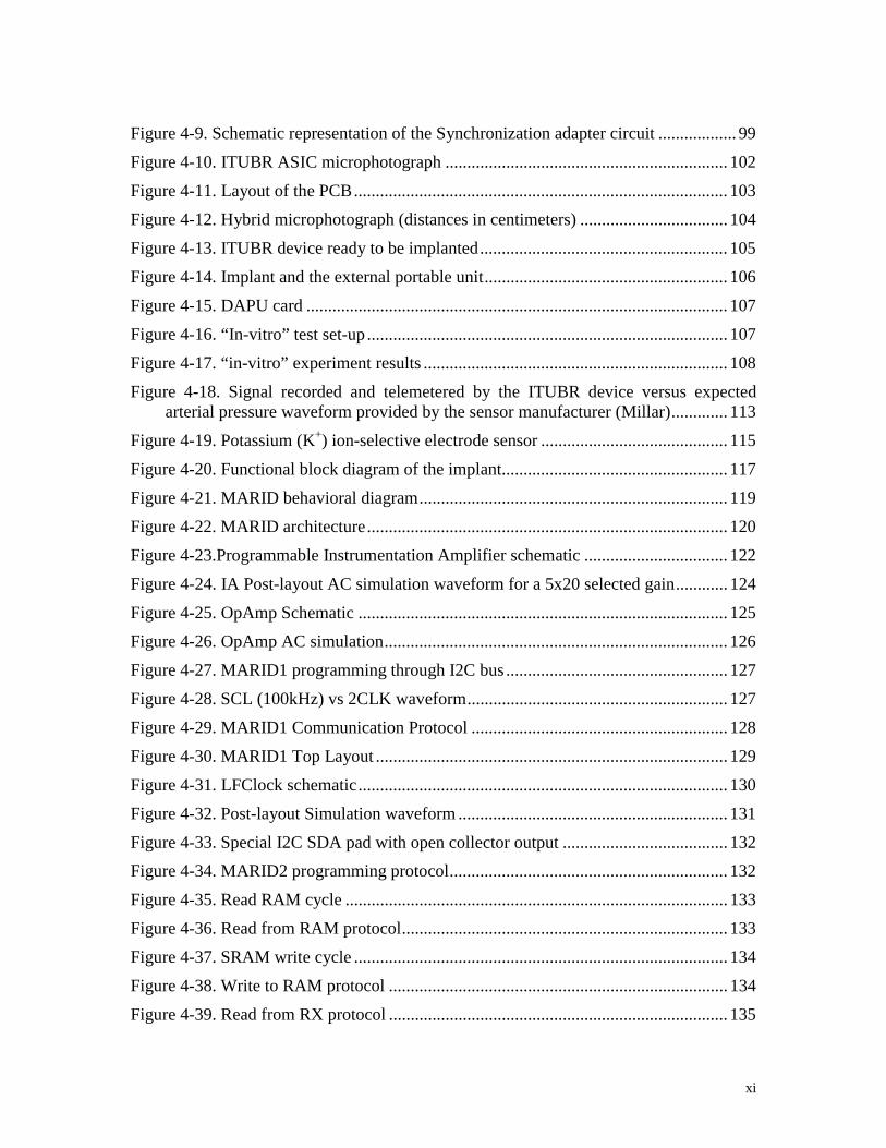
xi
Figure 4-9. Schematic representation of the Synchronization adapter circuit .................. 99
Figure 4-10. ITUBR ASIC microphotograph ................................................................. 102
Figure 4-11. Layout of the PCB...................................................................................... 103
Figure 4-12. Hybrid microphotograph (distances in centimeters) .................................. 104
Figure 4-13. ITUBR device ready to be implanted......................................................... 105
Figure 4-14. Implant and the external portable unit........................................................ 106
Figure 4-15. DAPU card ................................................................................................. 107
Figure 4-16. “In-vitro” test set-up ................................................................................... 107
Figure 4-17. “in-vitro” experiment results ...................................................................... 108
Figure 4-18. Signal recorded and telemetered by the ITUBR device versus expected arterial pressure waveform provided by the sensor manufacturer (Millar)............. 113
Figure 4-19. Potassium (K+) ion-selective electrode sensor ........................................... 115
Figure 4-20. Functional block diagram of the implant.................................................... 117
Figure 4-21. MARID behavioral diagram....................................................................... 119
Figure 4-22. MARID architecture................................................................................... 120
Figure 4-23.Programmable Instrumentation Amplifier schematic ................................. 122
Figure 4-24. IA Post-layout AC simulation waveform for a 5x20 selected gain............ 124
Figure 4-25. OpAmp Schematic ..................................................................................... 125
Figure 4-26. OpAmp AC simulation............................................................................... 126
Figure 4-27. MARID1 programming through I2C bus ................................................... 127
Figure 4-28. SCL (100kHz) vs 2CLK waveform............................................................ 127
Figure 4-29. MARID1 Communication Protocol ........................................................... 128
Figure 4-30. MARID1 Top Layout ................................................................................. 129
Figure 4-31. LFClock schematic..................................................................................... 130
Figure 4-32. Post-layout Simulation waveform .............................................................. 131
Figure 4-33. Special I2C SDA pad with open collector output ...................................... 132
Figure 4-34. MARID2 programming protocol................................................................ 132
Figure 4-35. Read RAM cycle ........................................................................................ 133
Figure 4-36. Read from RAM protocol........................................................................... 133
Figure 4-37. SRAM write cycle ...................................................................................... 134
Figure 4-38. Write to RAM protocol .............................................................................. 134
Figure 4-39. Read from RX protocol .............................................................................. 135

xii
Figure 4-40. Write to TX protocol .................................................................................. 135
Figure 4-41. MARID2 Top Layout ................................................................................. 136
Figure 4-42. MARID1 photograph ................................................................................. 137
Figure 4-43. MARID2 photograph ................................................................................. 137
Figure 4-44. MARID implant system prototype board ................................................... 137
Figure 4-45. External reader with Transmitter board (left) and receiver board (right)... 138
Figure 4-46. MARID device versus standard ORION instrument.................................. 140
Figure 4-47. Interface diagram of a TIC chip ................................................................. 142
Figure 4-48. TIC block diagram...................................................................................... 143
Figure 4-49. Startup sequence......................................................................................... 145
Figure 4-50. ETU to PIC data transference..................................................................... 146
Figure 4-51. PIC to ETU data transference..................................................................... 147
Figure 4-52. PIC to TIC to 8bits Command data transference........................................ 148
Figure 4-53. ETU to TIC to serial data transference....................................................... 149
Figure 4-54. TICv1.0 Top Layout................................................................................... 149
Figure 4-55. TIC microphotograph ................................................................................. 150
Figure 4-56. Clock setting to 427kHz ............................................................................. 151
Figure 4-57. ETU ⇒ TIC ⇒ Serial delay....................................................................... 151
Figure 4-58. Serial ⇒ TIC ⇒ ETU................................................................................. 152
Figure 4-59. ETU ⇒ TIC ⇒ PIC.................................................................................... 152
xiii
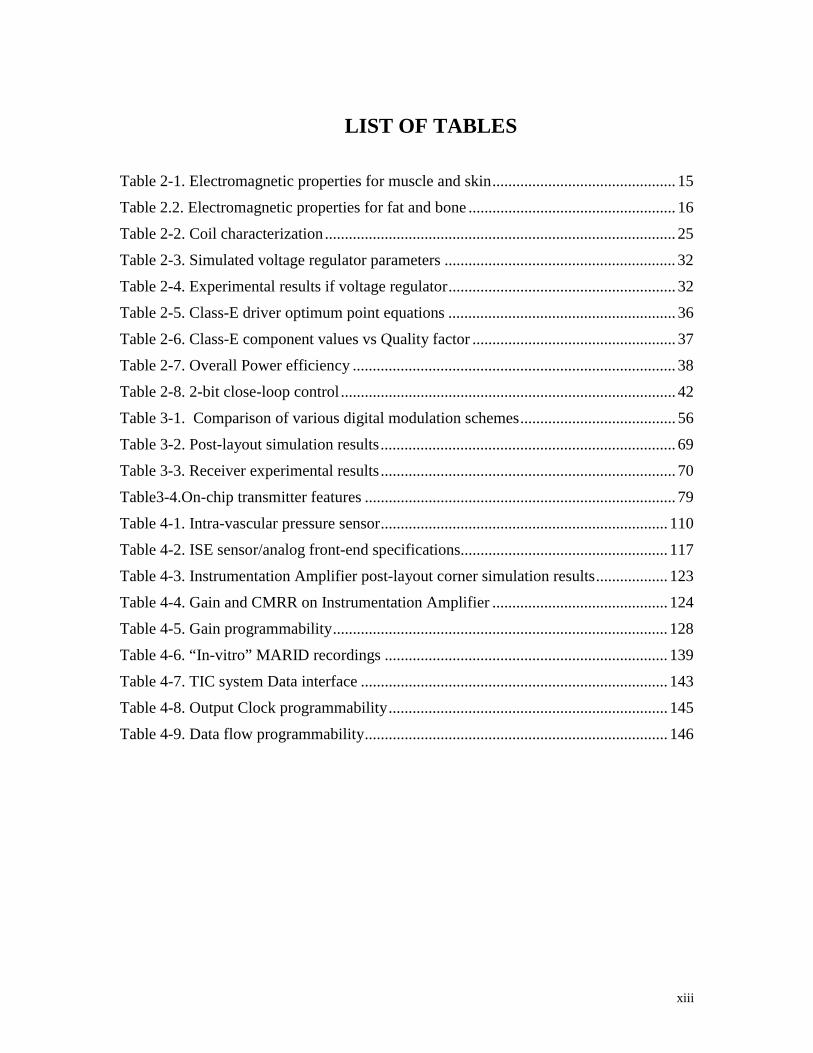
LIST OF TABLES
Table 2-1. Electromagnetic properties for muscle and skin.............................................. 15
Table 2.2. Electromagnetic properties for fat and bone .................................................... 16
Table 2-2. Coil characterization........................................................................................ 25
Table 2-3. Simulated voltage regulator parameters .......................................................... 32
Table 2-4. Experimental results if voltage regulator......................................................... 32
Table 2-5. Class-E driver optimum point equations ......................................................... 36
Table 2-6. Class-E component values vs Quality factor ................................................... 37
Table 2-7. Overall Power efficiency ................................................................................. 38
Table 2-8. 2-bit close-loop control .................................................................................... 42
Table 3-1. Comparison of various digital modulation schemes....................................... 56
Table 3-2. Post-layout simulation results.......................................................................... 69
Table 3-3. Receiver experimental results .......................................................................... 70
Table3-4.On-chip transmitter features .............................................................................. 79
Table 4-1. Intra-vascular pressure sensor........................................................................ 110
Table 4-2. ISE sensor/analog front-end specifications.................................................... 117
Table 4-3. Instrumentation Amplifier post-layout corner simulation results.................. 123
Table 4-4. Gain and CMRR on Instrumentation Amplifier ............................................ 124
Table 4-5. Gain programmability.................................................................................... 128
Table 4-6. “In-vitro” MARID recordings ....................................................................... 139
Table 4-7. TIC system Data interface ............................................................................. 143
Table 4-8. Output Clock programmability...................................................................... 145
Table 4-9. Data flow programmability............................................................................ 146
1
CHAPTER ONE
INTRODUCTION
1.1 OVERVIEW OF IMPLANTABLE ELECTRONIC DEVICES
In the recent years a very challenging product line of the biomedical industry has
emerged, with a fast-growing market and a even more promising future: implantable
electronic devices.
Surprisingly enough the concept of using electricity for medical purposes is not
a new idea. Roman physicians in the early years after the birth of Christ recommended
the electrical discharge of the torpedo fish for the treatment of headache and gout [1].
Volta and others made important contributions in the understanding of the relationship
between electricity and biology, but we had to wait many years to see these old concepts
to become part of standard therapy in modern medicine in the form of implantable
electronic devices.
The first and probably the most successful implantable electronic device up to
date is the pacemaker. Like all other implantable applications was initially implemented
with external/surface electrodes in the nineteen thirties [2]. The second generation was a
partially implantable system with leads coming out of the skin [3] but discomfort and
especially risk of infection were major problems. So finally the last and obvious step
was to create a fully implantable pacemaker. By mid 1950s [4], Dr. Rune Elmqvist
designed the world’s first implantable pacemaker and in late fifties Arn Larsson was the
lucky recipient of the first implanted pace. He was a forty-three years old patient who
suffered from life-threatening Adams-Stokes seizures. His condition was so bad that it
required thirty resuscitations per day. Doctor Senning implanted this pacemaker on
October 8, 1958. Mr. Larson had no complications and was still leading an active life by
1995 [5]. Nowadays approximately 600,000 pacemakers are implanted annually and an
estimated 3,000,000 people are living with functional pacemakers. The number of

2
patients receiving pacemakers is increasing at a rate of about 8% per year as the
population ages. The current market for cardiac pacemakers is around $3.36
billion/year.
Figure 1-1. Commercial pacemaker (courtesy of Pacesetter)
Following the pacemaker, a second implantable device was coming on the way:
implantable defibrillator. During late 60s the first of its kind was developed by Dr.
Micheal Mirowski [6]. Since then, this type of device has been very successful, with a
typical annual growth of 20-30% toping above 100,000 units per year. Even though
these two applications are clearly the “driving force” of the biomedical electrical
implant business, new emerging technologies/applications are coming along which can
potentially revolutionize certain areas of the medicine. Among others, I would mention
the new line of implantable electrical neuromodulation devices and other
neuroprosthesis as well as implantable drug delivery systems.
The key concept of electrical neuromodulation is to develop an interface
between the nervous system and an electronic device. Learning how to do it is a
combination of electrode, electronics and packaging technologies, where experts in
heterogeneous fields like material science, microelectronics, electrochemists,
biomedicine, cybernetics, etc work together. Interacting bi-directionally with the
nervous system opens a door towards new ways of treating diseases that have some
neurological basis. In the group of sensory prosthesis the cochlear implant is the most
accomplished example. The first direct stimulation of the auditory nerve in man was
carried out by Lundber in 1950 and later by Djourno and Eyries in 1957 [7]. Nowadays

3
the technology has improved so much (better electrodes, more channels, better signal
processing) that state-of-the-art cochlear implants (like the one in Figure 1-2) may even
provide the so called “super-hearing” where patients can hear even better than normal
people under certain noise conditions. This technology certainly changes the life of
many people. In the photograph bellow a little girl with a facial expression between joy
and surprise the first time in her life that she experienced a sound.
Figure 1-2. Commercial Cochlear implant.
Courtesy of Advanced Bionics Corp. Figure 1-3. Expression of joy/surprise of a little girl the first time she heard a sound.
In the same path but with substantially more way to go are the visual prosthesis.
Different approaches of how to interface with the visual cortex (either through retina
stimulation [8] [9] [10], through the optical nerve [11] [12] or directly stimulating the cortex [13]
[14]) are currently under development. Still within the electrical neuromodulation
business a set of ambitious large-market applications are being pursued. Among others
applications to treat urinary incontinence [15][16], pain management [17], movement
disorders [18], Parkinson’s disease [19], depression, etc. are also under way with a
perspective of a market of vast proportions, that will be able to improve the life quality
of millions.
Implantable drug delivery systems are also experiencing a substantial growth
recently. Developments in micro-dose delivery devices and specially a huge and
growing diabetic population are moving forward this field. An example of this is the so-
called artificial pancreas, that would replace completely the functionality of the
pancreas (segregate insulin when required) with an implantable insulin pump in
conjunction with a glucose sensor [20]. With this new device, occasional refills (maybe

4
once a month) of a transcutaneous chemical container will be the only activity required
by the type I diabetes patients.
In general, all these devices have some kind of bio-compatible body-to-
electronics interface (electrodes, sensors, ...) with two major activities : (1) modulating
locally the electric field (current or voltage stimulation) or delivering chemical
substances (micro-dose delivery) and (2) sensing a particular body activity (bio-signals
recording, biochemical concentration, etc.). In many cases both directions are desirable
in order to close the loop and provide a “self-contained” behavior of the implant. As
typical example and mentioned earlier, would be the new generation of artificial
pancreas: an insulin-injector delivers to the blood flow a controlled quantity of insulin
depending on the sensed levels of glucose in the blood. Other close-loop controls can be
found for example in the area of FES (Functional Electrical Stimulation): a paralyzed
patient can potentially regain control of a limb with the proper sensing and stimulating
interfaces to his skeletal muscle system.
For all this kind of old needs, only new emerging technologies can give the clue
to solve the difficulties and system complexities and bring up feasible devices. Among
all these new technologies with no doubt microelectronics plays a major role.
Within the biomedical industry developing implantable devices, three key-points
are a major concern for the engineers: reliability, miniaturization, and lifetime. All these
three topics can be handled more effectively if microelectronics, and particularly
Application Specific Integrated Circuits (ASICs) technologies are used. Improvement
in reliability is assured due to the intrinsic performance in this feature of a monolithic
silicon circuit. Moreover custom-made integrated circuits allow a dramatic reduction in
the number of of-the-shelf components (System-on-Chip approach), thus leading to a
smaller device, which ultimately also improves reliability. Finally, lifetime
(explantation is something everyone wants to avoid) can be increased due to power
reductions that can hardly be accomplished if a customized chip is not developed.

5
It is clear that to have a reliable, small and durable device is a mandatory fact in
the implant world. In terms of functionality an electronic implant can be described as
follows:
Figure 1-4. General purpose electronic implant
A so-called front-end section interfaces wireless with the external world by
means of getting bi-directional data and eventually energy if a batteryless or a
rechargeable battery is on board. In the biological-end there are some analog circuits
interfacing with the biological media (either for sensing or actuating). And in the middle
some sort of DSP (either digital or mixed-mode) is implemented. All these within a
hermetically sealed package with possibly some feed-through interfacing the electrodes.
1.2 SCOPE AND STRUCTURE OF THE THESIS
The present thesis describes the work done by the candidate in the scope of the
Grup d’Aplicacions Biomèdiques (GAP) within the National Center of Microelectronics
of Bellaterra. During the period 1996-1998 the candidate enjoyed a full-time grant (beca
pre-doctoral FPI Generalitat de Catalunya) including a year visit at Case Western
Reserve University (Cleveland, Ohio)/The University of Memphis (Tennessee) during
1998.
The work, developed within several projects, had the continuity necessary to
define a compact scope in the field of biomedical implants. In particular solving
problems of energy management resulting in the first generation of RF inductive links
developed in the CNM-UAB (chapter two). Concerning to the wireless data links
different solutions are presented for both batteryless (the first high-bandwidth bi-
6
directional telemetry system developed in the CNM-UAB) or battery operated implants
(ultra-low-power operation) (chapter three).
It is important to mention that what really rounds the content of the thesis is the
actual system-level implementation of the modular solutions presented in both chapters
two and three. All this is presented (chapter four), where three different systems are
depicted involving different levels of development.
The first application is the development of a fully implantable batteryless system
for bio-signal recording [21] [22] [23] within the European sponsored project Implantable
Telemetry System for Biomedical Research (ITUBR) led by the CNM-Barcelona. The
work done by the candidate goes from system specifications, all the way down to
implant development (including a custom ASIC conforming a System-on-Chip SoC
solution) and parts of an external controller. The involvement also included final “in-
vitro” and most importantly “in-vivo” bio-signal recordings, performed in a dog with
the device implanted and monitored by a portable external controller/reader that
recorded the data. That represented the first fully implantable wireless biomedical
device developed in the CNM-UAB to be actually implanted with bio-recordings.
The second application, that included the system level design and a prototype
board including two custom ASICs was done in the US in a combined visit at Case
Western Reserve University and The University of Memphis. The aim was to obtain a
long-term implantable chemical sensor with capability of storage of massive data [24].
“In-vitro” data was also obtained. As opposed to the ITUBR device, a battery was used
in here. Therefore the lifetime of the device was critical related to the power
consumption. Low power solutions (in system level as well as modular level) were
mandatory.
Finally, the third system-level work was not targeting any specific application.
The goal, re-using the existing modular hardware developed previously, was to create a
single chip to be used in any biomedical implant [25] offering a solution to energy and
data needs. The chip was created within the CNM-GAB with a collaboration from the
IBMT Institute (Fraunhoffer Institute for Biomidicine at St. Ingbert, Germany).

7
1.3 REFERENCES
[1] McNeal 1977 pp3-35
[2] W. Greatbatch, "Cardiovascular technology: origins of the implantable Cardiac
Pacemaker," The Journal of the Cardiovascular Nursing Vol. 5(3), pp.80-85, April
1991.
[3] K.A. Ellenbogan, Cardiac Pacing, Chapter 1, pp. 1-10, Blackwell Scientific
Publications, 1992.
[4] Anonymous, "Implantable electronic pace-makers," The Journal of Medical
Electronics, Vol. 1, pp.15-16, 1962.
[5] R.D Gold, "Cardiac pacing-from then to now," Medical Intsrumentation, Vol. 18(1),
pp. 15-21, Jan-Feb 1984.
[6] D.W Benson, D.S. Druz, J. Jude, and G. Knickerbocker, "Defibrillation," Journal of
the Association for the Advancement of Medical Instrumentation, Vol. 3(1), pp.53-
69, January 1969
[7] Clark, G.M., Pyman, B.C. and Bailey, Q. (1979) Journal of Laryngology and
Otology, 93:215-223
[8] Humayun, M., et al. "Visual Perception Elicited by Electrical Stimulation of Retina
in Blind Human", Arch. Ophtalmology, 114, 40-46, 1996
[9] Liu, W., McGucken, E., Clements, M., DeMarco, S. C, Vichienchom, K., Hughes, C.,
Humayun, M., de Juan, E., Weiland, J., Greenberg, R., "An Implantable Neuro-
stimulator Device for a Retinal Prosthesis", (International Solid-State Circuits
Conference, Feb 1999).

[10] Zrenner E, Stett A, Weiss S, Aramant RB, Guenther E, Kohler K, Miliczek K-D,
Seiler MJ, Haemmerle H (1999). Can subretinal microphotodiodes successfully
replace degenerated photoreceptors? Vision Research 39: 2555-2567
[11] C. Veraart, C. Raftopoulos, D. Pins, J. Delbeke, J.T. Mortimer, M.C. Wanet, G.
Michaux, O. Glineur, A. Vanlierde, Optic nerve electrical stimulation in a retinitis
pigmentosa blind volunteer. Soc. Neurosci. Abstr., 1998, 24: 2097.
[12] C. Veraart, J. Delbeke, M.-C. Wanet-Defalque, A. Vanlierde, G. Michaux, S.
Parrini, O. Glineur, M. Verleysen, C. Trullemans, T. Mortimer, Selectve
stimulation of the human optic nerve. Proceedings of the 3rd Conference of the
International Functional Electrical Stimulation Society (D. Popoviç, editor),
Sendai, Japan, August 23-27, 1999, in press.
[13] Schmidt, E. M., Bak, M. J., Hambrecht, F. T., Kufta, C. V., O'Rourke, D. K., and
Vallabhanath, P.: Feasibility of a visual Prosthesis for the blind based on
intracortical microstimulation of the visual cortex. Brain 119: 507-522, 1996.
[14] Hambrecht, F. T.: Visual prostheses based on direct interfaces with the visual
system. In: Bailliere's Clinical Neurology Vol.4 #1, G. S. Brindley and D. N.
Rushton eds., Tindall, London, 1995.
[15]Bent AF, Sand, PK, Ostergard, DR, Brubaker, L. (1993) Transvaginal electrical
stimulation in the treatment of genuine stress incontinence and detrusor instability
Int Urogynecol J . 14:9-13.
[16] JL Buller, GW Cundiff, KA Noel, KS Leffler, JA VanRooyen, RM Ellerkman*, and
AE Bent, "RF BION™: An injectable microstimulator for the treatment of
overactive bladder disorders in adult females". American Urogynecologic Society
(AUGS), Chicago 2001
[17] Shealy CN, Mortimer JT, Reswick JB. Electrical inhibition of pain by stimulation of
the dorsal columns: preliminary clinical report. Anesth Analg 1967;46:489-91.

[18] Benabid et al. Chronic electrical stimulation of the ventralis intermedius nucleus of
the thalamus as a treatment of movement disorders. J Neurosurg 1996; 84:203-14.
[19] Starr et al. Ablative surgery and deep brain stimulation for Parkinson’s disease.
Neurosurgery 1998; 43:989-1015.
20 Minimed Inc. Northridge, California
[21] J. Parramon, P. Doguet, D. Marin, M. Verleyssen, R. Muñoz, L. Leija, E.
Valderrama, “ASIC-based batteryless implantable telemetry microsystem for
recording purposes”, 19th International conference of the IEEE Engineering in
medicine and biology society- EMBS’97, Chicago (USA) Oct 97
[22] O. Scholz, J. Parramon, J.-U. Meyer, E. Valderrama, "The design of an implantable
telemetric device for the use in neural prostheses", XIV International Symposium
on Biotelemetry, Marburg (Germany), Apr.97
23 I. Rincon, A. Garcia-Rozo et al. “Telemetric monitoring of left ventricular pressure in
a canine model of acute normovolemic hemodilution”, ASAIO journal 44(2):84A,
1998.
[24] J. Parramon, B. D. Pendley, C. Rowan and M. R. Neuman , “An Integrated Sensor-
Memory-Telemetry System”, XV International Symposium on Biotelemetry,
Alaska 1999
[25] D. Marín, O. Scholz, J. Parramon, T. Osés, J. Meyer, E. Valderrama. "Fast
prototyping of implantable systems for stimulation and recording based on a bi-
directional and rf-powered telemetry integrated circuit". 6th Vienna International
Workshop on Functional Electrostimulation (IFESS'98). Proceedings. September.
1998, Vienna (Austria), pp. 81-84


11
CHAPTER TWO
TRANSCUTANEOUS POWER TRANSMISSION
2.1 INTRODUCTION
Any kind of device (electronic, mechanic, etc..) needs energy to become
functional. So a concern for any system engineer is to be sure that power will be always
there when required. In many easy-to-supply devices the problem related to power is
essentially associated to cost. But in the micro implant world the problem of power goes
beyond economics and becomes something essential in terms of functionality. Due to the
usual small amount of energy available (small batteries) the way the engineer manages
power becomes a key point in this industry. One of the focuses of this dissertation is to
try finding paths to improve this parameter, what at the end means to increase the
expected life-time of the device, and thus improving the life-quality of the subject
carrying the implant.
The most common approach to provide energy to the implant is to use an energy-
container, typically an electrochemical “deposit” like batteries. Due to the push in needs
of the industry (specially in the portable communication systems sector), improvements
in energy density and miniaturization have been accomplished. The new generation of
primary Lithium cells [1] is a good example of that. Despite of these improvements there
is still a long way to go. Other energy-container-like devices seem to be a promising
future trend, especially with the new thin-film super-capacitors [2].
The above solution has a clear problem: as the energy source is embedded, once
exhausted an explantation is mandatory to provide new energy. So the only chance we
have to avoid surgical procedure is using an external source to deliver wireless energy in

12
order to (1) recharge the implanted batteries (using secondary batteries like Li-ion [3]) or
(2) provide on-line power to the system. The latter refers to electromagnetic powering
(EMP) of the system, which includes two main options: (1) RF going from a few kHz to
few Mhz or (2) infrared up to light.
The first one has been widely proved as useful [4], thus permitting a reasonably
easy development, especially when power needs are high (above 10mW). The infrared
option has its own chances. Main interest of this approach is the small size of the implant
that can be achieved, due to the use of photo diodes despite coils as receivers. But the
power efficiency is very poor [5], hence non-practical for many implant applications and
only useful for low-power transference. A third and more unexplored way is to find the
power source in the same body, like thermal [6] or kinetic energy. But again very small
amounts of energy can be supplied which in most of the cases make this solution useless.
Clear constrains in power demand makes the RF option the most atractive. Main
idea of RF power is the use of magnetic energy stored in an external coil. When another
coil is placed in the surroundings a coupling between both coils appear, and through
electromagnetic induction a certain amount of voltage in the secondary (internal coil) is
transferred from the external-primary tank. To understand better the concept we could
also use a capacitor rather than a coil (so switching the magnetic field by an electrical
field), but the capacitance value would be very low (capacitance coupling would be much
smaller than magnetic coupling) and the power transference consequently would also be
very poor.
Figure 2-1. RF powering system
L2 C2 R2
Internal-Secondary
W,Io
L1
K
Skin
External-Primary

13
This technique as said, commonly referred as RF Powering, uses two coupled
coils, the transmitter (primary) which is externally but close-to-the-skin positioned, and
the receiving (secondary) which is a part of the implantable device. In this chapter, one of
the first power systems using the RF technique that operates in the range of 10-20MHz is
described. Previous works reported in the field used lower frequencies up to 1-2MHz [7].
Our approach makes compatible the power transfer with elevate communication
bandwidth sharing the carrier for both purposes. In order to do so we had to push the
frequency limits to regions were losses are difficult to avoid due to the intrinsic trade-off
between power and frequency in any switching network. This chapter shows primarily
the power system developed within the ITUBR project including a coil design and
development, a custom-made chip receiver and an external transmitter
Within the RF-link analysis a novel mathematical analysis for very-low coupling
factor is presented, which goes beyond current existing studies [8], and includes in the
model the parasitic resistance of the coil, which proved to be very critical specially in the
case where micro-coils are required. Finally two novel ideas concerning loop-control are
proposed to further enhance the overall power efficiency of any RF link, especially
relevant in our case were high frequencies yield to external transmitter losses.
2.2 ELECTROMAGNETIC COMPATIBILITY
This first part summarizes a very important issue concerning inductive power
systems and its industrial way out: Electromagnetic compatibility (EMC). By definition is
the ability of electronic devices or systems to operate in their intended environments
without suffering or causing intolerable electromagnetic interference (EMI). For an active
medical implant, EMC means that (1) it does not induce harmful effects to the patient’s
health and does not interfere with other nearby electronic equipment, and (2) it functions
properly when exposed to the electromagnetic fields anticipated in the patient’s
environment. Epidemiological studies [9] suggested some connections between
electromagnetic energy and biological disorders. In the RF powering approach, the

14
magnetic field generated by the external coil will interact with the patient’s biological
systems as well as with the implanted electronics. Despite the magnitude of the field in
most cases is much smaller than other medical applications (like magnetic resonance
imaging), it still produces measurable tissue heating [10] and some concern about safety
regulations may certainly apply. An overview of the basic questions related to powering
is presented next.
i) Electrical properties of tissue.
Most of the studies concerning the electrical properties of tissues were carried out
during the 40’s and 50’s [11] [12]. Tissues are composed of cells filled primarily with fluids
and encapsulated by thin membranes. The intracellular fluid consists of various salt ions,
polar protein molecules, and polar water molecules. The extra-cellular fluid is similar to
the intracellular fluid except that it has different proportions of the elements. When an
AC signal is applied the oscillations of the free charges (ions) give rise to conduction
currents (Eddy currents) and the rotation of dipole molecules at the frequency of the
applied field effect displacement currents. This phenomenon is the basis for the
biological reactions to electromagnetic fields. Power dissipation in tissue, resulting from
ohmic losses associated with the conduction currents and dielectric losses associated with
displacement currents, provide the energy necessary to induce most of the biological
reactions to em fields (as we will analyze in part ii).
The electrical properties of any material and by extension any tissue can be
summarized within the complex permittivity ε*. Mathematically can be defined as:
where ε0 is the permittivity in vacuum, ε’ is the relative permittivity (dielectric
constant) of the media, and ε’’ is the loss factor. The effective conductivity of the media
due to the sum of conduction current losses and dielectric losses is:
and the loss tangent is: [13][14]
)’’’(0 εεεε j−=∗
’’0εωεσ =
’’’
’
0εωεσ
εεδ ==tan

15
Next table (Table 2.1) shows some relevant constants of biological substances and
its dependence on frequency. Ideally for a material without losses the effective
conductivity should be zero, meaning that no conduction or displacement currents have
been generated. For high water content tissue (like muscle and skin) the conductivity
increases with frequency from 0.4mho/m at 1MHz to 10.3mho/m at 10GHz. This
increase in effective conductivity means a decrease in depth of penetration, which is
defined as the depth at which eddy current density has decreased to 1/e or about 37% of
the surface density. In this case at 1MHz the em field penetrates 91.3cm and at 10GHz
around 0.34cm.
For low water content tissue (like fat and bone) the same dependence with
frequency appears. In this case tough, the absorption is smaller and the depth of
penetration is larger compared to the high water content tissue.
Table 2-1. Electromagnetic properties for muscle and skin
Muscle, Skin, and Tissues with High Water Content Frequency
(MHz) Wavelength in Air
(cm) Dielectric Constant εD
Conductivity ρL
(mho/m)
Wavelength λL
(cm)
Depth of Penetration
(cm)
1 30000 2000 0.400 436 91.3 10 3000 160 0.625 118 21.6
27.12 1106 113 0.612 68.1 14.3 40.68 738 97.3 0.693 51.3 11.2 100 300 71.7 0.889 27 6.66 200 150 56.5 1.28 16.6 4.79 300 100 54 1.37 11.9 3.89 433 69.3 53 1.43 8.76 3.57 750 40 52 1.54 5.34 3.18 915 32.8 51 1.60 4.46 3.04 1500 20 49 1.77 2.81 2.42 2450 12.2 47 2.21 1.76 1.70 3000 10 46 2.26 1.45 1.61 5000 6 44 3.92 0.89 0.788 5800 5.17 43.3 4.73 0.775 0.720 8000 3.75 40 7.65 0.578 0.413 10000 3 39.9 10.3 0.464 0.343

16
Table 2.2. Electromagnetic properties for fat and bone
Fat, Bone, and Tissues with Low Water Content Frequency
(MHz) Wavelength in
Air (cm) Dielectric Constant εD
Conductivity ρL (mho/m)
Wavelength λL (cm)
Depth of Penetration (cm)
1 30000 10 3000
27.12 1106 20 10.9-43.2 241 159 40.68 738 14.6 12.6-52.8 187 118 100 300 7.45 19.1-75.9 106 60.4 200 150 5.95 25.8-94.2 59.7 39.2 300 100 5.7 31.6-107 41 32.1 433 69.3 5.6 37.9-118 28.8 26.2 750 40 5.6 49.8-138 16.8 23 915 32.8 5.6 55.6-147 13.7 17.7 1500 20 5.6 70.8-171 8.41 13.9 2450 12.2 5.5 96.4-213 5.21 11.2 3000 10 5.5 110-234 4.25 9.74 5000 6 5.5 162-309 2.63 6.67 5800 5.17 5.05 186-338 2.29 5.24 8000 3.75 4.7 255-431 1.73 4.61 10000 3 4.5 324-549 1.41 3.39
ii) Biological effects.
Most of the literature concerning biological effects refers to low frequency (20-
200Hz) or high frequency (200MHz-200GHz) ranges. So in our working range (1-
30MHz) there is still a big lack of experimental data. There are two main effects to be
considered: (1) thermophysiological, that is the capability of the thermoregulatory system
in tolerating tissue heating due to e.m. field, and (2) athermal, where the field acts upon
cellular structures.
In the first case the heating effects are not harmful as long as induced heat does
not exceed the metabolic rate of an adult, which is about 1Watts/kg. In the second case it
is well accepted from in-vitro and in-vivo studies that damage can be caused to the cell,
mainly within the plasma membrane, by the EM fields [15]. Many additional effects
(action potential disturbance, DNA synthesis alteration, etc.) are still unclear.

17
iii) Safety standards.
In 1966 a limit of safe exposure to electromagnetic radiation was established y the
ANSI at 10mW/cm2, assuming that (1) thermally induced alterations were the only
mechanism of biological effects and (2) by limiting the tissue heating by 1°C or less
adverse bio-effects would be avoided. Recently the energy absorption in tissue was
recognized as a much more realistic parameter than simply temperature rise. So a new
magnitude, the SAR (Specific Absorption Rate) defined as the rate of energy dissipated
per unit of mass was introduced. Mathematically we have SAR=σE2/2ρ where σ is the
electrical conductivity of the medium, E is the dissipated energy and ρ is the mass density
of the medium.
ANSI developed a set of safety standards in 1982 revised by IEEE in 1991. Based
in the most accepted RF exposure threshold to produce behavioral changes in animals
(SAR=4W/Kg) the standard of safety was set with a security factor of 10. So
SAR=0.4W/Kg for whole-body average. But local peaks of SAR can be tolerated far
above this value. Specifically the spatial peak SAR value averaged over any 1g of tissue
in cubic shape should not exceed 8W/Kg, except for ankles, wrists, hands and feet, where
SAR averaged over any 10g of tissue should not exceed 20W/Kg. Moreover, any device
radiating 7W or less with the radiator not within 2.5cm from the body it is considered
safe and excluded from the above standards [16].
Exposures in excess of the standard may not be harmful, but are not recommended
in absence of benefits. Other relevant conclusions from available literature include (1)
damages from exposure to electromagnetic fields over separate periods are not
cumulative, and (2) whole-body SAR is proportional to any partial body SAR when
responding to the change in field strength .

18
iv) Safety concerns in Inductive Powered Implants.
The RF powering system considered here, where the maximum power radiated
goes bellow 7W and the field generated is near field (decays very rapidly) makes the
subject of implantation the only person whose safety should be studied. In most of the
cases the 0.4W/Kg whole-body average is easily accomplished, so the concern is about
local SAR peaks near the external coil.
v) Implant EMI protection
Obviously the electromagnetic field generated by the coils may well be a source
of Electromagnetic Interference to (1) the external electronics surrounding the patient and
to (2) the implanted electronics. In order to avoid the first problem the frequency chosen
should be compatible with any radio-device near the implant and other instrumentation
and if possible compatible with the FCC part 15 rules [17]. The second problem is usually
solved by using metal encapsulation of the whole active implanted circuitry except (in the
case of RF power) by the receiver coil that should be unshielded in order to receive
energy.
As a matter of conclusion, we have seen that tissue absorption increases with
frequency [see section i)]. So for the same amount of power required by the implant the
transmitter will have to deliver more energy to compensate the loss. Depending on the
package type, the case absorption may play a major role. The implant industry uses
metallic casing for most of the long-term implants. And metal is a “electromagnetic
hungry” material, that is, absorbs radiation very easily (and it heats up), especially for
higher frequencies. So again the lower the frequency the safer and the more reliable the
system. But there are other constrains that may point out towards higher frequencies,
especially the communication bandwidth. Somehow a trade-off between all this
parameters has to be reached in order to fulfill all the specs and build up a reliable and
safe power transfer. The basic rule of thumb concerning RF power could be: choose the

19
lowest power transmission frequency compatible with the bandwidth constrains of the
system and compliant with the FCC rules of maximum emitted radiation.
2.3 INDUCTIVE LINK
A RF power system includes three different elements: the inductive link
(essentially a pair of coils), the implanted receiver and the external transmitter. This
section focuses in the inductive link. Coil design as well as other link analysis will be
investigated to obtain a reliable and efficient high-bandwidth RF powering system.
2.3.1 Basic concepts
An inductive link is basically a pair of coupled coils defining a transformer with a
certain coupling factor. Physically the parameter to measure is the Mutual inductance
between two coils (M). In a quasi-static approach were current changes are slow enough
to consider the magnetic field in each instant identical to the one produced with a steady
current, the electromotive force (EMF) induced in the secondary is proportional to the
time-derivative of the primary current (figure 2-2). The constant of proportionality is M,
the so-called Mutual Inductance [18]. Sometimes it is more useful the concept of coupling
factor, defined as:
sp LL
Mk =]1.2[
Where Lp is the primary (external) coil inductance and Ls is the secondary
(internal) coil inductance (see figure 2-1).

20
dt
dIMEMF p=
pI pLsL
sp LL
Mk =
Figure 2-2. Basic transformer with secondary EMF
The k factor is generally more suitable as a design parameter because it does not
depend on the number of coils (the M-dependence is canceled with the Li dependence),
thus making the analysis a little bit simpler.
In any case the amount of energy transferred depends greatly on this coupling
what ultimately defines the power efficiency of the link and the tolerance of the system to
lateral and angular misalignments.
2.3.2 Mutual inductance studies
In order to design properly the coils, a study concerning calculation of Mutual
inductance (M) and coupling factor (k) must be done. Taking the definition of M [14] we
have:
∫ ∫⋅
=12
210
4]2.2[
r
dldlM
πµ
The mutual inductance of two circular air-cored loops (µr=1) whose axes are
parallel (radii a and b, coil distance d) and with no misalignment can be expressed in a
single integral [19][20]:
wherekGabdbaM )(),,(]3.2[ 0µ= 22)(
4
dba
abk
++≡ )(
2)()
2()( rR
rrKr
rrG −−≡

21
Where K(k) and E(k) are the complete elliptic integrals of the first and second
kind respectively. This expression assumes a wire radius much smaller than both coil
radius (a and b). See figure 2-3.
Figure 2-3. Coil to coil positioning with lateral misalignment
In case we have a lateral misalignment ρ (defined as the distance between the axes
of both coils as seen in figure 2-3) we define the following parameters:
φρρ cos222 bbbL ++≡ φρ
φρβcos+
≡b
sintan
Then the mutual inductance will become:
∫= wheredrGab
abM
L
φβπ
µ)(
cos
2]4.2[ 0
22)(
4
dba
abr
L
L
++≡
In case of ρ different to zero it is impossible to integrate exactly, so we must go
towards a numerical integration. The formula [2.4] only refers to single-turn coils. In
order to calculate mutual inductance for multi-turn coils we used a simplified approach.
The approach used to calculate the mutual inductance between two coils separated a
distance d, with a certain length (l1 and l2), number of turns (N1 and N2) and radii (a and
b) is as follows:

22
22**],,[]5.2[ 21’
21’ ll
ddwhereNNdbaMM loopsigle ++== −
Basically this approximation gives accurate results as long as the distance
between coils is much larger than the length of the two coils. Next graphic (Figure 2.4)
shows a comparison between the theoretical values obtained once solved numerically1 the
integral [2.4] (with the approximation [2.5]) and the experimental values obtained in the
lab, in a non-misalignment case.
-2 0 2 4 6 8 10 12 14 16
1,0
1,5
2,0
2,5
3,0
3,5 experimental Results
calculated ResultsM [nH]
d [mm]
Worst caseregion
Figure 2-4. Mutual inductance experiments
The error of the theoretical approach, which considers planar coils at an additional
distance of the average coil length increases as the distance between the coils decreases.
In the area of our interest (from 5mm to 12mm) this approach has a maximum error of
21% at 5mm decreasing down to 6% at 12mm. The case with misalignment was also
verified experimentally with similar results showing greater accuracy at larger distances.
So basically we have proved that the calculation method that will be used extensively
1 The numerical calculations were performed with the software Mathematica™.

23
when designing the coils is reasonably accurate in the operating range, especially in the
upper distance range (around 1 cm). This is very important because that region defines
the worst-case scenario of power transfer.
2.3.3 Coil development
The methodology used to design the coils is based in theoretical calculations of
Mutual Inductance using the formulas presented above. Throughout this analysis
optimum coil geometry is obtained. And once determined the optimum geometry the
coils have been fabricated and characterized.
2.3.3.1 Coil Design
In order to achieve a good efficiency and to maintain a high tolerance to
misalignments, the diameter of the inner coil should be as big as possible. In our case, a
diameter of 10mm was chosen constrained by the implant size. Next, with a given
operating distance and tolerance field, the diameter of the external coil was determined.
As depicted in Figure 2-5, there is a maximum of mutual inductance versus external coil
diameter for each operating distance. By using a small coil diameter, higher M should be
expected for small distances. The general rule is that for small geometry the magnetic
density can achieve larger values for close distances, but also decays faster, and therefore
its variation with misalignment is much lager (see figure 2-6). So there is a trade-off
between peak values and misalignment tolerance. Our range of operation, defined by the
medical staff, lies between d=5mm, ρ=0 and d=12mm, ρ=12mm with a nominal
operating distance of 8mm. Comparing figures 2-5 and 2-6 we see that for the nominal
distance (d=8mm) we have a M-peak around D1(external diameter) of 24mm. But the
misalignment in the worst case is not that good. A compromise to select the diameter was
taken with a final value of external diameter of 30mm. The M-value is fairly close to the
peak for a nominal 8mm distance. And the misalignment figures are much better, with
almost no change in M all over the working range. So a diameter ratio of 3 between the
external and the internal coil will be used.

24
Figure 2.5. M(Y-axis) vs external coil diameter
D1 (D2=10mm) Figure 2.6. M(Y-axis) vs lateral misalignment
Delta; d=8mm
In contrast to the mutual inductance, the coupling factor is independent of the
number of turns and only depends on geometry. This makes the value interesting for
general studies.
Through calculations, it is possible to find the best and the worst case coupling k
for this particular case (though disregarding angular displacements):
Mmin = 0,929nH ⇒ kmin = 0,032 @ d=12mm, ρ=12mm
Mmax = 2,954nH ⇒ kmax = 0,1 @ d=5mm, ρ=7mm
Another possibility to optimize the coil design would be to try to work near the
critical coupling [21]. The concept of critical coupling is essentially the following: for
larger distances (as showed in detail in 2.3.4 [2-8]) the power transfer increases
monotonously with M or k (as the intuition would say) but at very small distances (high
M) the second order effect of the Mutual Inductance (reflection from the secondary to the
primary) may have a bigger negative contribution than the first order effect (linear
electromotive force proportional to M), thus defining a certain M-region where the power
transfer has a maximum. Therefore near the maximum there is a region of very small first
order variations. The problem is that the coupling in that region describes a fairly sharp
dddddddd
d
d
External coil diameter [mm]
nominalcase M
[nH]
25
high-Q shape, thus only small variations of k (or M) can be accommodated.
Unfortunately looking at the wide range of possible variation of the M (or k) for our
application (from 0.929nH to 2.954nH) due to the distance and lateral misalignment
variations, the critical coupling approach is not practical.
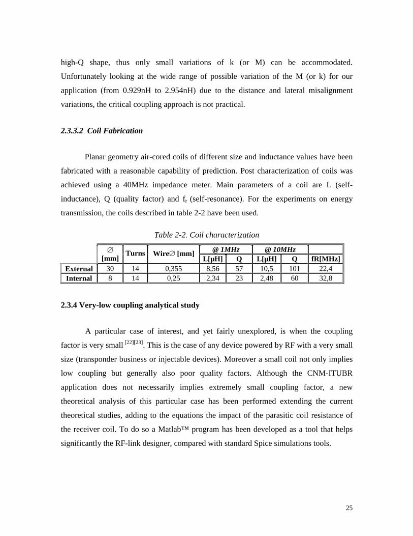
2.3.3.2 Coil Fabrication
Planar geometry air-cored coils of different size and inductance values have been
fabricated with a reasonable capability of prediction. Post characterization of coils was
achieved using a 40MHz impedance meter. Main parameters of a coil are L (self-
inductance), Q (quality factor) and fr (self-resonance). For the experiments on energy
transmission, the coils described in table 2-2 have been used.
Table 2-2. Coil characterization
@ 1MHz @ 10MHz
[mm]
Turns Wire [mm] L[µH] Q L[µH] Q fR[MHz]
External 30 14 0,355 8,56 57 10,5 101 22,4 Internal 8 14 0,25 2,34 23 2,48 60 32,8
2.3.4 Very-low coupling analytical study
A particular case of interest, and yet fairly unexplored, is when the coupling
factor is very small [22][23]. This is the case of any device powered by RF with a very small
size (transponder business or injectable devices). Moreover a small coil not only implies
low coupling but generally also poor quality factors. Although the CNM-ITUBR
application does not necessarily implies extremely small coupling factor, a new
theoretical analysis of this particular case has been performed extending the current
theoretical studies, adding to the equations the impact of the parasitic coil resistance of
the receiver coil. To do so a Matlab™ program has been developed as a tool that helps
significantly the RF-link designer, compared with standard Spice simulations tools.

26
Next picture shows a typical Voltage-in Voltage-out (Serial-in Parallel-out) link
configuration.
C s
L s R 2
K
W , I o
L p
R 1
C p
V 1
V 2
Figure 2-7. Voltage-in Voltage-out RF link
Essentially the best efficiency occurs when the output impedance of the primary
source matches with the network. It has been shown [24] that the voltage gain transfer
function can be found us:
21
12211
2 1]6.2[
RL
RLkL
M
V
V
+=
For a fixed secondary load the power increases with the voltage. So in order to
optimize the power transfer one should basically go to the prior mentioned critical
coupling point kc, defined by the condition [2.7]:
0]7.2[1
2 =
∂∂
= ckkV
V
k
1
2
2
1
1
2]8.2[R
R
L
Lk
V
V=
In the case of extremely small coupling factor (k2<<1) the second order effects of
the coupling factor are neglected, so the gain transfer is given by [2.8]. This formula
basically tells that the higher the coupling factor and the smaller the secondary
inductance the better the efficiency, for a constant load and an optimized primary circuit.
This is not the case in reality when you must include in the model the losses of the
receiver coil.

27
A calculation method using Maxwell equations to evaluate the power transfer is
presented next. The transformer within the Voltage-in/Voltage-out configuration (Figure
2.7) can be modeled as follows.
C s
ε s
R load
V out
_
+
R s V in
C p
ε P
R P
i p
i s r in
Figure 2.8. Equivalent model of Voltage-in/Voltage-out Link
Using the third Maxwell equation in the quasi-static approach the next set of
equations follows:
dt
diL
dt
diLLk p
ps
spp −=ε]9.2[ dt
diL
dt
diLLk s
sp
sps −=ε]10.2[
And solving the circuit network:
)1
(]11.2[sC
rRiVp
inpppin ++=+ ε )1
(]12.2[sCR
RRi
sload
loadsss +
+=ε
Assuming that the inductance of the secondary coil towards the primary coil may
be far weaker than the self-inductance of the primary coil (small coupling factor) we
have:
dt
diLLl
dt
d
dt
diL
dt
d ssp
pp =<<= 1121]13.2[
φφ
Combining [2.9] plus [2.11] with the [2.13] first order approach and [2.10] plus
[2.12] and solving the differential equation we finally obtain:
,)(
]14.2[ wheresLRrR
M
V
V
ssinpin
out
+Θ+Θ
+= ω
sCR
R
sload
load
+≡Θ
1]15.2[

28
This is the Voltage Gain transfer function taking into account the non-ideal
parameters of the coil (finite Q). It can be easily proved that for the case without parasitic
resistance we recover the expression [2.8].
The theoretical effort has been basically carried out to decrease design time.
Obviously you can go to the electric simulator, but if many parametrical sweeps are
required the computation time grows too fast. A comparison between the analytical first-
order method using Matlab and the exact Spice calculations was performed. The
difference in design time is significant. Using HP workstation with Eldo™ simulator it
took about 1 hour including real computation time plus design time to carried a set of
parametric sweeps. Each data point in a Gain-transfer diagram was actually obtained by
finding the peak-point of an AC analysis. As opposed to that, a simple Matlab™ program
using the [2.14] equation can perform the analysis in about 10 seconds. Obviously the
Eldo™ simulated results are more accurate, but with small coupling factor (bellow 0.02)
the first-order approach proves to be very accurate (see Figure 2-9). First-order
theoretical calculations computed with Matlab™ are the continuous line.
0 10 20 30 40 50 60 70 0
0.1
0.2
0.3
0.4
0.5
0.6
0.7 Theoretical vs simulated k=0.0015 Rload=1.6k
Ls (uH)
Gain
--Theoretical
* Simulated
f=2.0MHz
f=1.5MHz
f=1.0MHz
f=0.5MHz
Figure 2-9. Non-approximate simulations versus first-order analytical approach

29
This theoretical approach using first order approximation is also usefull to have a
better comprehension of the link itself, giving a simple way of understanding how each
variable impacts the overall transfer. For instance within the k<<1 approach there is no
critical coupling because the higher the Mutual Inductance the better the gain. Also it can
be seen that for any given frequency there is a critical secondary inductance (Ls,crit) where
the Gain is maximum.
2.4 INTERNAL POWER RECEIVER
This section describes the design of the implanted RF Power receiver, developed
in the framework of the CNM-ITUBR project. In order to pick up the incoming RF
energy a special circuit was used to handle high input voltages above 20 volts. The front-
end receiver was a tuned LC tank matched to the transmitter frequency. Thus depending
on the coupling factor (which varies with distance, orientation, etc.. see section 2.3.2) a
certain voltage signal is induced. Amplitude ranges can go up to 60V peak-to-peak, if
strong coupling and very efficient power transmitter applies. Figure 2-10 shows the
energy-receiver circuit implemented.
+_
Linear regulator+-
Bandgap reference
+_
Linear regulator
+_
Linear regulator
5V Analog supply 2.5V reference5V Digital supply
Voltageprotection
Figure 2-10. Energy-receiver circuit
Once induced the signal in the terminals of the receiving coil, the AC signal is
full-rectified using a Schottky-diode bridge, hence defining two output nodes: ground and

30
rectified voltage. In the next stage the incoming voltage is pre-regulated using a
characterized zener diode and a NPN transistor which at the same time is acting as an
input voltage protector of 11.7V threshold. Through the use of a double BandGap voltage
reference, a final dual 5V supply lines (analog and digital) plus a 2.5V reference is
obtained using three output buffers with resistor-ratio programmed gain stages (series
regulator).
2.4.1 Integration
In this section, some of the key elements in the design of the energy front-end in
terms of chip design are presented.
i) Technology: The concern of dealing with large input voltages was the major
constrain for choosing a certain IC technology. Through Europractice program the best
solution was to use the ALCATEL-MIETEC 2.4um CMOS process with a certain
changes in the fabrication steps in order to include high voltage gates (up to 50V) and
also bipolar transistors. The process is named HBIMOS.
ii) LC front-end: The 5-20MHz range of the RF powering did not allow
integration of the coil either the capacitance. Typical values of these integrated elements
are bellow 1 µH with very low Qs for the coils and hundreds of picofarads for the
capacitors. Hand-made air coils (section 2.3.3.2) and commercial trimming capacitors
were used to match the frequency.
iii) Diode bridge: A great concern in power efficiency was given to the full-wave
rectifier, because a bad switch time in the diode may results in very big power loses due
to large dropping voltage in the diodes terminals. A first trial intending to integrate the
diodes into the HBIMOS technology [25] showed very poor switching times, thus we had
no other chance than using a special high-speed high-voltage Schottky diodes for the
rectifier bridge.
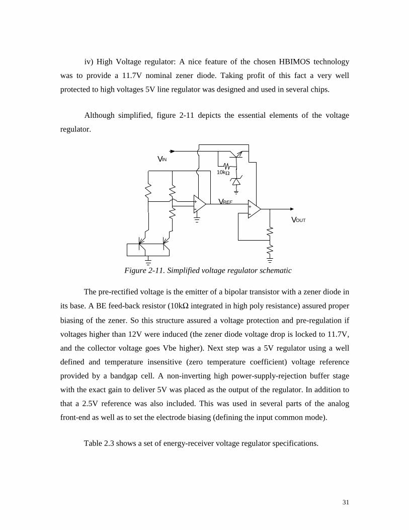
31
iv) High Voltage regulator: A nice feature of the chosen HBIMOS technology
was to provide a 11.7V nominal zener diode. Taking profit of this fact a very well
protected to high voltages 5V line regulator was designed and used in several chips.
Although simplified, figure 2-11 depicts the essential elements of the voltage
regulator.
Figure 2-11. Simplified voltage regulator schematic
The pre-rectified voltage is the emitter of a bipolar transistor with a zener diode in
its base. A BE feed-back resistor (10kΩ integrated in high poly resistance) assured proper
biasing of the zener. So this structure assured a voltage protection and pre-regulation if
voltages higher than 12V were induced (the zener diode voltage drop is locked to 11.7V,
and the collector voltage goes Vbe higher). Next step was a 5V regulator using a well
defined and temperature insensitive (zero temperature coefficient) voltage reference
provided by a bandgap cell. A non-inverting high power-supply-rejection buffer stage
with the exact gain to deliver 5V was placed as the output of the regulator. In addition to
that a 2.5V reference was also included. This was used in several parts of the analog
front-end as well as to set the electrode biasing (defining the input common mode).
Table 2.3 shows a set of energy-receiver voltage regulator specifications.
V IN
V REF + - +
- V OUT
10kΩ

32
Table 2-3. Simulated voltage regulator parameters
DC input range Load sensibility DC sensibility Power@7V 7 to 20 V <1mV/kΩ <0.3mV/V 1.08mW7V
2.4.2 Results
Once translated to silicon the on-chip receiver had an overall area of
880x800 µm2, including the zener-based pre-regulator, the bandgap voltage reference, the
current generator and three buffered voltage lines each including a low PSRR OpAmp.
Figure 2-12 shows a microphotograph of the circuit:
Figure 2-12. On-chip energy receiver microphotograph (HBIMOS technology)
Table 2-4 shows the experimental data of the supply line provided by the energy
receiver integrated within the CNM-ITUBR system.
Table 2-4. Experimental results of the voltage regulator
DC input range Load sensibility DC sensibility Power@7V
7.1 to 20 V <1.6mV/kΩ <0.9mV/V 1.12mW7V
Figure 2-13 shows the regulated output as a function of the induced voltage.
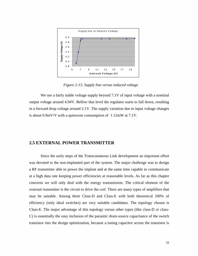
33
Figure 2-13. Supply line versus induced voltage
We see a fairly stable voltage supply beyond 7.1V of input voltage with a nominal
output voltage around 4.94V. Bellow that level the regulator starts to fall down, resulting
in a forward drop voltage around 2.1V. The supply variation due to input voltage changes
is about 0.9mV/V with a quiescent consumption of 1.12mW at 7.1V.
2.5 EXTERNAL POWER TRANSMITTER
Since the early steps of the Transcutaneous Link development an important effort
was devoted to the non-implanted part of the system. The major challenge was to design
a RF transmitter able to power the implant and at the same time capable to communicate
at a high data rate keeping power efficiencies at reasonable levels. As far as this chapter
concerns we will only deal with the energy transmission. The critical element of the
external transmitter is the circuit to drive the coil. There are many types of amplifiers that
may be suitable. Among them Class-D and Class-E with both theoretical 100% of
efficiency (only ideal switches) are very suitable candidates. The topology chosen is
Class-E. The major advantage of this topology versus other types (like class-D or class-
C) is essentially the easy inclusion of the parasitic drain-source capacitance of the switch
transistor into the design optimization, because a tuning capacitor across the transistor is
S up p ly line vs Ind uc e d V o lta g e
3 .8
4 .0
4 .2
4 .4
4 .6
4 .8
5 .0
5 7 9 1 1 1 3 1 5 1 7 1 9
In d u c e d V o lta g e (V )
Su
pp
ly V
olt
age
(V)

34
required. Another reason, now dealing with the communication itself, is the fact that a
simple supply modulation results directly in amplitude modulation of the coil current [20].
2.5.1 Class-E design
The class-E amplifier was introduced in 1975 by Sokal and Sokal [26]. It is a very
interesting structure when high power efficiency is a primary concern. A simple class-E
driver consists of a transistor with a shunt capacitor, a RF choke inductor to provide a
constant current from the power supply and a series RLC load network which is tuned to
a certain frequency. The basic scheme is shown in figure 2-14. In this scheme the
inductance of the RLC series circuit will be the transmitting antenna in the telemetry
system. This configuration is a multi-frequency load network because there are two
relevant resonance frequencies: the series resonance of the RLC network and the parallel
resonance of the total shunt capacitance (Cshunt plus the parasitic drain-source capacitance
of the transistor (Cds)) together with the RLC network.
Figure 2-14. Class-E coil driver
The transistor is driven by a periodic signal acting as a switch. The transistor can
be a FET or a BJT. In what follows we use a MOSFET. The drain-source voltage is
determined by the transistor when it is ON (very close to ground) and by the transient
response of the load network when it is OFF. As we will show in the next paragraph we
take advantage of this fact to reduce the switching losses in the transistor.

35
The high efficiency of class-E amplifiers is achieved by reducing the transistor
switching losses in the following ways:
i) The transistor is turned-on when the drain voltage has come back to zero,
reducing the turn-on loss.
ii) The slope of the drain voltage is also zero at the time of turn-on, which allows
for slight detuning without loosing efficiency.
The above two conditions define the optimum point of operation or class-E point
where the maximum efficiency and maximum output power in class-E drivers is reached.
The class-E operation point of the amplifier was analyzed by Raab [27], giving a simple set
of equations for a 50% duty cycle of the transistor operation (D=0.5, see Table 2-5). A
more complete analysis, also for idealized operation, is presented by Kazimierczuk in [28].
In this article the design of class E drivers working in the optimum point operation is
shown for different switch duty cycle (D) and quality factor of the RLC network (Q).
However, to simplify the generation of the carrier frequency, we will consider 50%
switch duty cycle, as is the case in most class-E drivers.
The main assumptions taken are: (1) the current through the RF choke is constant;
(2) the quality factor of the RLC series circuit is high enough to presume the output
current (through the RLC circuit) is sinusoidal; (3) the transistor has zero saturation
voltage (in case we consider a BJT), zero on-resistance and infinite off-resistance and
(4) the total shunt capacitance is independent of the drain voltage (i.e. the influence of the
variation of the parasitic capacitances with the drain voltage are not considered).

36
Table 2-5. Class-E driver optimum point equations
Parameter definition Equations for D=0.5 Eq. Nº
RT = total load resistance. RScoil = coil resistance at switching frequency
f, ω=2πf. Re = series resistance reflected to the class E
driver from the resistive load across the receiver coil.
R R R RT LOAD Scoil e= + + (1)
CTSHUNT = Total shunt capacitance (CSHUNT+CDS)
C
RTSHUNTT
=⋅
1
5 4466, ω (2)
X = series reactance at f frequency.
X LC
RTT
T= − = ⋅ωω
111525, (3)
VDS_PEAK = maximum amplitude in the drain to source voltage.
IDS_PEAK = maximum amplitude in the drain to source current.
V V
IDS PEAK CC
DS PEAK CC
_
_
,
,
= ⋅= ⋅
3 56
2 84 I
(4)
(5)
Vt = amplitude of the AC signal through the transmitter inductor LT.
V Vt CC= ⋅1 074, (6)
RDC = equivalent resistance that the amplifier shows to the power supply VCC.
R RDC T= ⋅17337. (7)
PIN= input power PV
RINcc
DC=
2 (8)
|iC| = amplitude of the AC current though RT. iV
RCCC
T
=⋅1 074,
(9)
These assumptions are acceptable for low frequencies (less than 5MHz) where the
turn-on and turn-off time of the transistor are negligible. At higher frequencies, the values
of the components become only an approximation and they have to be adjusted to achieve
the optimum operating point. From these equations the main components values and
characteristics (e.g. the maximum ratings of the transistor) can be derived.
Using the result obtained in section 2.3.3.1 a ration of 3 between external and
internal coil was chosen (minimizing lateral misalignment impact), with an external coil
diameter of 30mm. With that dimension a coplanar 1µH coil with a resistance of 494mΩ

37
at 10MHz was used as an input of the design. Hence following the Kazimierczuk
equations the table 2-6 was obtained.
Table 2-6. Class-E component values vs Quality factor
Kazimierczuk Table Component values calculation Qt *Lt/R *R*Ct *R*CSH R () Ct (pF) CSH (pF) fRLC (MHz) foff (MHz)
1 2,104 2,104 0,2204 29,86 1121,33 117,46 4,75 15,43 2 2,85 0,7124 0,219 22,05 514,29 158,10 7,02 14,47 3 3,75 0,4166 0,215 16,76 395,72 204,23 8,00 13,71 5 5,673 0,2269 0,2067 11,08 326,05 297,03 8,81 12,76 7 7,642 0,156 0,2017 8,22 301,98 390,44 9,16 12,19
10 10,62 0,1062 0,1971 5,92 285,69 530,21 9,42 11,68 15 15,61 0,06936 0,1931 4,03 274,25 763,53 9,61 11,20 20 20,6 0,05149 0,1909 3,05 268,68 996,12 9,71 10,94 100 100,58 0,01006 0,1851 0,62 256,30 4715,83 9,94 10,20
Finally a Quality Factor (Qt) of 5 was chosen because although it provides less
output power for the same power supply voltage, the variations in the coupling with the
receiver do not lead to a considerable decrease of the efficiency and at the same time is
low enough to allow high-bandwidth modulation. The choke inductance should guarantee
that the supply current of the class E amplifier stays approximately constant during the
RF cycle. The relationship between its value and the switching frequency is usually
defined by:
LR
fCHOKET
C
> ⋅35.
The power switching transistor of the class-E driver is a N-channel Enhancement-
Mode MOS VN66AFD transistor with 66V maximum drain source voltage, 1 A
maximum DC current and 15 ns rise and fall time. The package of this transistor is a TO-
220 that allow easy placement of a heat sink.

38
Induced V oltage vs distance
0
10
20
30
40
50
60
70
80
90
0.0 0.5 1.0 1.5 2.0 2.5 3.0 3.5
dista nce (cm)
Ind
uce
d V
olt
ag
e (
V)
2.5.2 Results.
The measurements done on the class-E driver operating at 10MHz show
transmitter efficiencies above 70%. In terms of overall power efficiency (transmitter +
link + receiver) next table (Table 2.7) shows the results obtained at a fixed nominal
distance (6mm) and with a 1.5kΩ load (emulating implant equivalent consumption).
Table 2-7. Overall Power efficiency
fT (MHz) VCC (V) ICC (mA)
V(V) @ 1.5K Power to the load Global Efficiency
T 11 5 270 18 0.216W 16% 11 10 390 29 0.560W 14.3%
So transmitter efficiencies above 70% and global efficiencies of power transfer in
the range of 15% were reached. Values that can be considered as pretty good due to the
big constrain imposed by the high values of carrier frequencies if compared with former
RF Powering systems developed.
In terms of distance of operation and misalignment sensibility figures 2-15 and
2-16 show the results obtained.
Figure 2-15. Induced Voltage versus distance

39
Induced voltage vs latera l m isalignment (12mm)
0
10
20
30
40
50
60
0 2 4 6 8 10
Late ral misaligm ent (m m)
Ind
uce
Vo
lta
ge
(V)
Vpp (Volts)
We see that for closer distances very large current can be achieved (up to 80V).
Enough power was transferred for all distance range of operation (defined as 15mm). The
minimum voltage to operate was around 7V, so with this system we could successfully
transmit the required energy to a distance larger than 30mm.
Figure 2-16. Induced Voltage versus lateral misalignment
Due to the 3:1 diameter ratio chosen the misalignment tolerance is fairly good.
Even for a misalignment of the same magnitude of the implanted coil we have a voltage
reduction of only about 20%.
The angular variation was also investigated. In that case we see a change in 18%
of the induced voltage for a 15-degree angular misalignment at a distance of 17mm (see
figure 2-17).

40
Figure 2-17. Induced Voltage versus angular misalignment
2.5.3 New design solutions to improve power transfer efficiency
Despite the driver efficiency achieved is rather good ( around 70% see section
2.5.2), two new ideas to improve the overall link efficiency are presented.
2.5.3.1 Close-loop induced voltage control
This idea implies a close-loop control of the transferred voltage using the back-
telemetry channel. Essentially a continuous monitoring of the induced voltage in the
implant is sent back to the external unit that processes the information and reduces or
increases the amount of energy transmitted as needed. As seen in figure 2-18.
Induced Voltage vs Angular misalignment (17mm)
0
5
10
15
20
25
30
0 2 4 6 8 10 12 14 16
Angular misalignment (degree)
Ind
uce
d V
otl
age
(V)
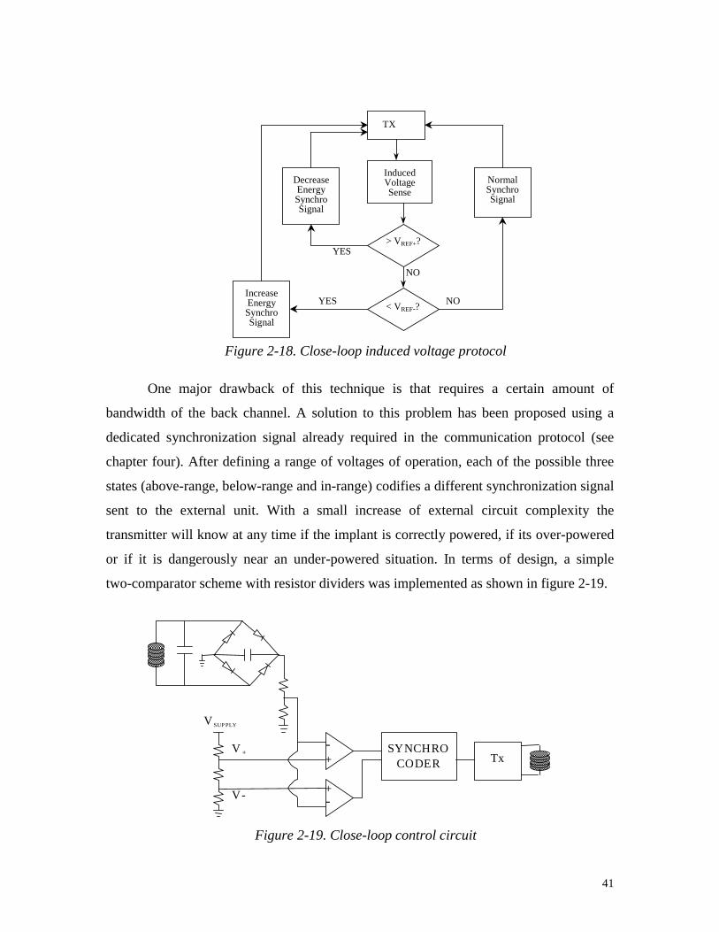
41
Figure 2-18. Close-loop induced voltage protocol
One major drawback of this technique is that requires a certain amount of
bandwidth of the back channel. A solution to this problem has been proposed using a
dedicated synchronization signal already required in the communication protocol (see
chapter four). After defining a range of voltages of operation, each of the possible three
states (above-range, below-range and in-range) codifies a different synchronization signal
sent to the external unit. With a small increase of external circuit complexity the
transmitter will know at any time if the implant is correctly powered, if its over-powered
or if it is dangerously near an under-powered situation. In terms of design, a simple
two-comparator scheme with resistor dividers was implemented as shown in figure 2-19.
+-
+-
SYNCHROCODER Tx
V+
V-
V SUP PLY
Figure 2-19. Close-loop control circuit
YES
TX
InducedVoltageSense
DecreaseEnergySynchroSignal
NormalSynchroSignal
> VREF+?
< VREF-?IncreaseEnergySynchroSignal
NOYES
NO

42
Two voltage references defining the upper and lower voltage range of operation
are compared with the incoming previously divided induced voltage. The three states are
codified as shown in table 2-8.
Table 2-8. 2-bit close-loop control
Below-range In-range Over-range Bit0 0 0 1 Bit1 1 0 0
Each of the three possible states is sent to the external controller through the back-
telemetry channel. In order to not interfere with the standard communication protocol and
also without wasting bandwidth. There is a dedicated hard-coded synchronization signal
(used to robust the communication) for each of the three states.
This concept was introduced in the TIC chip (see chapter four, section 4.3) where
a general purposed chip interface providing energy and data to any implant is described.
2.5.3.2 Class-E self-adaptation design
The class-E circuit can be optimized in different ways if stand-alone, that means if
no influence of any reflected load. The major source of energy losses is due to the
switching losses when slightly out of tuning. As we have already seen in section 2.5.1
Kazimierzcuk et al showed a way of optimize the Class-E for different range of
frequencies and quality factors. Basically with the adequate inductance and capacitance
values the switch may turn ON just when there is a zero voltage drop across the drain-
source of the transistors (no energy stored in the series capacitance is lost). This approach
has the problem that for a variable impedance network (that’s the case of the transmitter
when different coupling factors in the link may define different reflected impedances)
you must change any of the passive elements up to reach again the optimum point. An
active circuit to detect the right moment to turn-on the switch has been also presented in
different papers [29] using a zero-crossing circuit controlling the gate-source voltage of the

43
switch. This idea works well and makes the class-E driver to operate with good
efficiencies with variable loads. But there is no control on the exact amount of energy
effectively transferred to the implant.
A novel power-adaptive system idea is presented, were through sensing the
primary-coil current the transmitter can evaluate the coupling factor (k) knowing the
secondary load as well as the rest of the network parameters (inductances and quality
factors).
Different authors have investigated the capabilities of sensing the reflected
impedance to achieve communication with the implant (see chapter three section 3.2.2.1).
The solution proposed here goes beyond that and extracts real coupling factor
information that will be used to optimize the power transfer link. As we see in Figure 2-
20 the reflected impedance is proportional to M2 and inversely proportional to the
secondary load.
Figure 2-20. Reflected impedance sensor
In a low frequency range most of the reflected impedance is real. The relation
between the primary current and the secondary parameters are as follows:
)(22
11
loadcoils R
MRR
VI
ω++=
C2
L2R2
M
L1
Rcoil
C1
V1
R1
2
22
R
MWZr =
44
Therefore if the inductances and quality factors of both primary and secondary
coils are known and if the secondary load is also pre-defined, then the mutual inductance
(M) and as a consequence the coupling factor (k) will be determined. This is the first step
to the magnetic field regulation. Once the coupling is known, it is possible to calculate
the exact magnetic field (primary current) required to meet the power requirements.
Essentially the concept here described is very similar to the one presented in section
2.5.3.1. In the former section the information about the coupling (coded in the induced
voltage) was sent back by telemetry means. In this section the method described do not
require any back telemetry, what simplifies the implant design (even though increases the
external controller complexity). Obviously this concept only can be used when
reasonably high coupling factors apply (hence the reflected impedance is measurable).
For low-coupling systems, the back-telemetry close-loop solution proposed earlier is still
the only feasible solution.

45
2.6 REFERENCES
1 Colin A. Vincent, Bruno Scrosati, "Modern Batteries, An introduction to
electrochemical power sources", Butterworth-Heinemann find supercapacitor
reference
2 B.E. Conway, "Electrochemical supercapacitors", Kluwer Academic/Plenum publishers,
New York
3 Galina Dern, "Advances in Li-ion and Li-polymer: comparison of Li-ion Prismatics vs
Polymers", Power’99, San Diego 1999
4 J.C. Schuder et al., “High level electromagnetic energy transfer through a closed
chestwall”, IER Int. Conv. Rec., pt.9,vol 9, pp.119-126, 1961.
5 D. Edell, "Chronically implantable neural information transducers", 18th Conference of
the IEEE EMBS, Mini-Symposium on Neurotechnology session, Nov’96
6 Applied Digital Solutions, "Miniaturized Thermoelectric Generator Powered by Body
Heat"
7 P. Troyk, M. Schwan, “Closed-loop class E transcutaneous power and data link for
microimplants”, IEEE Transactions on Biomedical Engineering, vol. 39, nº6, Jun’92
8 T. Akin, K. Najafi, R. Bradley, “An implantable multichannel digital neural recording
system for a micromachined sieve electrode”, 8th conference on solid-state sensors
and actuators, 51-54, June 95
9 T.S. Perry, “Today’s View of Magnetic Fields”, IEEE Spectrum, vol. 31, No.12, pp. 14-
23, 1994.

46
10 E. Hochmair, “System optimization for improved accurancy in transcutaneous signal
and power transmission”, IEEE transactions on biomedical engineering, vol. BME-
31, nº2, Feb'84.
11 J.M. Osepchuk (ed), Biological Effects of Electromagnetic Radiation. New Yor, NY:
IEEE Press, 1983.
12 H.P. Schwan, “Electrical Properties of Tissue and Cell Suspensions”, in J.H. Lawrence
and C.A. Tobias (eds.), Biological and Medical Physics. New York, NY: Academic
Press, 1957
13 C.C. Johnson and A.W. Guy, “Nonionizing Electromagnetic Wave Effects in
Biological Materials and Systems”, Proc. IEEE, vol.60, pp.692-18, 1972.
14 H.P. Schwan, “Electrical Properties of Tissue and Cell Suspensions”, in J.H. Lawrence
and C.A. Tobias (eds.), Biological and Medical Physics. New York, NY: .Academic
Press, 1957
15 S.F. Cleary, “Biological Effects of Radiofrequency Electromagnetic Fields”, in O. P.
Gandhi (de.), Biological Effects and Medical Applications of Electromagnetic
Energy. Englewood Cliffs, NJ: Prentice Hall, 1990.
16 The IEEE Standard for Safety Levels with Respect to Human Exposure to Radio-
Frequency Electromagnetic Field, 3 KHz to 300 GHz (IEEE C95.1-1991, Revision
of ANSE C5.1-1982). New York, NY: IEEE Press, 1991.
17 FCC rules and regulations , part 15
18 “The Feynman Lectures on Physics”, Volume II, Electromagnetism and matter

47
19 M. Soma, D. Galbraith, R. White, “Radio-frequency coils in implantable devices:
misalgnment analysis and design procedure”, IEEE transactions on biomedical
engineering, vol.BME-34,nº4,276-282, April 87
20 C. Zierhofer, E. Hochmair, "Coil desing for improved power transfer efficiency in
inductive links", 18th Conference of the IEEE EMBS, 5.8.2. Voice and
neuroprosthetic augmentation session, Nov’96
21 E. Hochmair, “System optimization for improved accurancy in transcutaneous signal
and power transmission”, IEEE transactions on biomedical engineering, vol. BME-
31, nº2, Feb'84.
22 G.E. Loeb, C.J. Zamin and J.H.Schulman, “Injectable microstimulator for functional
electrical stimulation”, Med.&Biol.Eng.&Comput., vol.29,pp.NS13-NS19, 1991.
23 M. Nardin, K.Najafi, “A multichannel neuromuscular microstimulator with bi-
directional telemetry”, 8th conference on solid-state sensors and actuators, 59-62,
Jun’95
24 T. Akin ,“An integrated telemetric multichannel sieve electrode for nerve regeneration
applications”, PhD dissertation, The University of Michigan, Ann Arbor, October
1994
25 J. Parramon, Internal CNM-GAB document. “Design of ITUBRv1.0 chip”
26 N.O. Sokal and A.D. Sokal, "Class E, a New Class of High Efficiency Tuned Single-
Ended Switching Power Amplifiers", IEEE Journal of Solid-State Circuits, Vol. 10,
pp 168-176, June 1975.
27 F. H. Raab, "Idealized Operation of the class E tuned power amplifier", IEEE
Transactions on Circuits and Systems, vol CAS-24, Nº 12, December 1977.
48
28 M.K. Kazimierczuk, K. Puczko, "Exact Analysis of Class E Tuned Power Amplifier at
any Q and Switch Duty Cycle", IEEE Transactions on Circuits and Systems, Vol.
CAS-34, Nº 2, February 1987
29 P. Troyk, M. Schwan, “Closed-loop class E transcutaneous power and data link for
microimplants”, IEEE Transactions on Biomedical Engineering, vol. 39, nº6, Jun’92