Embed Size (px)
Citation preview

MCP3905A/05L/06AEnergy Metering ICs with Active Real Power Pulse Output
Features• Supplies active (real) power measurement for
single-phase, residential energy metering• Supports IEC 62053 International Energy
Metering Specification and legacy IEC 1036/61036/687 Specifications
• Two multi-bit, DAC, second-order, 16-bit, Delta-Sigma Analog-to-Digital Converters (ADCs)
• Reduced pulse width of calibration output frequency and mechanical counter drive for low power meter designs (MCP3905L)
• Increased output frequency constant options for meter design (MCP3905L)
• 0.1% typical measurement error over 500:1 dynamic range (MCP3905A / MCP3905L)
• 0.1% typical measurement error over 1000:1 dynamic range (MCP3906A)
• Programmable Gain Amplifier (PGA) for small sig-nal inputs supports low value shunt current sen-sor:- 16:1 PGA - MCP3905A / MCP3905L- 32:1 PGA - MCP3906A
• Ultra-low drift on-chip reference: 15 ppm/°C (typ.)• Direct drive for electromagnetic mechanical
counter and two-phase stepper motors• Low IDD of 4 mA (typ.)• Tamper output pin for negative power indication• Industrial Temperature Range: -40°C to +85°C• Supplies instantaneous real power on HFOUT for
meter calibration
DescriptionThe MCP3905A/05L/06A devices are energy-meteringICs designed to support the IEC 62053 internationalmetering standard specification. They supply afrequency output proportional to the average active realpower, as well as a higher-frequency outputproportional to the instantaneous power for metercalibration. The MCP3905L offers reduced pulse widthof calibration output frequency and mechanical counterdrive for lower power meter designs. They include two16-bit, Delta-Sigma ADCs for a wide range of IB andIMAX currents and/or small shunt (<200 µOhms) meterdesigns. It includes an ultra-low drift voltage referencewith < 15 ppm/°C through a specially designed bandgap temperature curve for the minimum gradient acrossthe industrial temperature range. A fixed-function DSPblock is on-chip for active real-power calculation. A no-load threshold block prevents any current creepmeasurements. A Power-On Reset (POR) blockrestricts meter performance during low-voltagesituations. These accurate energy metering ICs withhigh field reliability are available in the industry standardpinout.
Package Type
Functional Block Diagram
FOUT0
DGNDNEG
1234
2423222120191817
5678
FOUT1
NCOSC2OSC1
DVDDHPF
AVDDNC
CH0+CH0-CH1-CH1+
HFOUT
169 G0MCLR1514
1011
G1F0
REFIN/OUTAGND
1312 F1F2
24-Pin SSOP
16-bit
ΔΣ ADC
MCLR
+
–
CH0+
CH0-
Reference2.4V
+
–
CH1+
CH1-
HPF1
LPF1 E-to-Fconversion
REFIN/
FOUT1
HFOUT
G0 G1
F2 F1FOUT0
OSC1 OSC2
OUT
NEG
HPF
F0Multi-level
16-bit
ΔΣ ADCMulti-level
X
HPF1
PGA
POR
© 2006 Microchip Technology Inc. DS22011A-page 1
MCP3905A/05L/06A
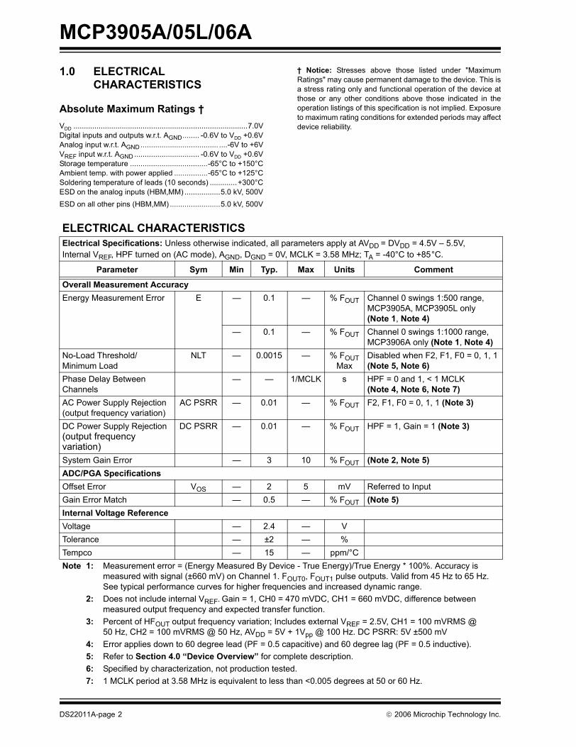
1.0 ELECTRICAL CHARACTERISTICS
Absolute Maximum Ratings †VDD ...................................................................................7.0VDigital inputs and outputs w.r.t. AGND........ -0.6V to VDD +0.6VAnalog input w.r.t. AGND ..................................... ....-6V to +6VVREF input w.r.t. AGND ............................... -0.6V to VDD +0.6VStorage temperature .....................................-65°C to +150°CAmbient temp. with power applied ................-65°C to +125°CSoldering temperature of leads (10 seconds) .............+300°CESD on the analog inputs (HBM,MM) .................5.0 kV, 500VESD on all other pins (HBM,MM) ........................5.0 kV, 500V
† Notice: Stresses above those listed under "MaximumRatings" may cause permanent damage to the device. This isa stress rating only and functional operation of the device atthose or any other conditions above those indicated in theoperation listings of this specification is not implied. Exposureto maximum rating conditions for extended periods may affectdevice reliability.
ELECTRICAL CHARACTERISTICSElectrical Specifications: Unless otherwise indicated, all parameters apply at AVDD = DVDD = 4.5V – 5.5V,Internal VREF, HPF turned on (AC mode), AGND, DGND = 0V, MCLK = 3.58 MHz; TA = -40°C to +85°C.
Parameter Sym Min Typ. Max Units Comment
Overall Measurement AccuracyEnergy Measurement Error E — 0.1 — % FOUT Channel 0 swings 1:500 range,
MCP3905A, MCP3905L only (Note 1, Note 4)
— 0.1 — % FOUT Channel 0 swings 1:1000 range, MCP3906A only (Note 1, Note 4)
No-Load Threshold/ Minimum Load
NLT — 0.0015 — % FOUTMax
Disabled when F2, F1, F0 = 0, 1, 1(Note 5, Note 6)
Phase Delay Between Channels
— — 1/MCLK s HPF = 0 and 1, < 1 MCLK(Note 4, Note 6, Note 7)
AC Power Supply Rejection(output frequency variation)
AC PSRR — 0.01 — % FOUT F2, F1, F0 = 0, 1, 1 (Note 3)
DC Power Supply Rejection(output frequency variation)
DC PSRR — 0.01 — % FOUT HPF = 1, Gain = 1 (Note 3)
System Gain Error — 3 10 % FOUT (Note 2, Note 5)ADC/PGA SpecificationsOffset Error VOS — 2 5 mV Referred to InputGain Error Match — 0.5 — % FOUT (Note 5)Internal Voltage ReferenceVoltage — 2.4 — VTolerance — ±2 — %Tempco — 15 — ppm/°CNote 1: Measurement error = (Energy Measured By Device - True Energy)/True Energy * 100%. Accuracy is
measured with signal (±660 mV) on Channel 1. FOUT0, FOUT1 pulse outputs. Valid from 45 Hz to 65 Hz. See typical performance curves for higher frequencies and increased dynamic range.
2: Does not include internal VREF. Gain = 1, CH0 = 470 mVDC, CH1 = 660 mVDC, difference between measured output frequency and expected transfer function.
3: Percent of HFOUT output frequency variation; Includes external VREF = 2.5V, CH1 = 100 mVRMS @ 50 Hz, CH2 = 100 mVRMS @ 50 Hz, AVDD = 5V + 1Vpp @ 100 Hz. DC PSRR: 5V ±500 mV
4: Error applies down to 60 degree lead (PF = 0.5 capacitive) and 60 degree lag (PF = 0.5 inductive).5: Refer to Section 4.0 “Device Overview” for complete description.6: Specified by characterization, not production tested.7: 1 MCLK period at 3.58 MHz is equivalent to less than <0.005 degrees at 50 or 60 Hz.
DS22011A-page 2 © 2006 Microchip Technology Inc.

MCP3905A/05L/06A
TEMPERATURE CHARACTERISTICS
Reference InputInput Range 2.2 — 2.6 VInput Impedance 3.2 — — kΩInput Capacitance — — 10 pFAnalog InputsMaximum Signal Level — — ±1 V CH0+,CH0-,CH1+,CH1- to AGNDDifferential Input Voltage Range Channel 0
— — ±470/G mV G = PGA Gain on Channel 0
Differential Input Voltage Range Channel 1
— — ±660 mV
Input Impedance 390 — — kΩ Proportional to 1/MCLK frequencyBandwidth(Notch Frequency)
— 14 — kHz Proportional to MCLK frequency, MCLK/256
Oscillator InputFrequency Range MCLK 1 — 4 MHzPower SpecificationsOperating Voltage 4.5 — 5.5 V AVDD, DVDDIDD,A IDD,A — 2.7 3.0 mA AVDD pin onlyIDD,D IDD,D — 1.2 2.0 mA DVDD pin only
Electrical Specifications: Unless otherwise indicated, VDD = 4.5V – 5.5V, AGND, DGND = 0V.
Parameters Sym Min Typ Max Units Conditions
Temperature RangesSpecified Temperature Range TA -40 — +85 °COperating Temperature Range TA -40 — +125 °C (Note)Storage Temperature Range TA -65 — +150 °C
Note: The MCP3905A/05L/06A operate over this extended temperature range, but with reduced performance. Inany case, the Junction Temperature (TJ) must not exceed the Absolute Maximum specification of +150°C.
ELECTRICAL CHARACTERISTICS (CONTINUED)Electrical Specifications: Unless otherwise indicated, all parameters apply at AVDD = DVDD = 4.5V – 5.5V,Internal VREF, HPF turned on (AC mode), AGND, DGND = 0V, MCLK = 3.58 MHz; TA = -40°C to +85°C.
Parameter Sym Min Typ. Max Units Comment
Note 1: Measurement error = (Energy Measured By Device - True Energy)/True Energy * 100%. Accuracy is measured with signal (±660 mV) on Channel 1. FOUT0, FOUT1 pulse outputs. Valid from 45 Hz to 65 Hz. See typical performance curves for higher frequencies and increased dynamic range.
2: Does not include internal VREF. Gain = 1, CH0 = 470 mVDC, CH1 = 660 mVDC, difference between measured output frequency and expected transfer function.
3: Percent of HFOUT output frequency variation; Includes external VREF = 2.5V, CH1 = 100 mVRMS @ 50 Hz, CH2 = 100 mVRMS @ 50 Hz, AVDD = 5V + 1Vpp @ 100 Hz. DC PSRR: 5V ±500 mV
4: Error applies down to 60 degree lead (PF = 0.5 capacitive) and 60 degree lag (PF = 0.5 inductive).5: Refer to Section 4.0 “Device Overview” for complete description.6: Specified by characterization, not production tested.7: 1 MCLK period at 3.58 MHz is equivalent to less than <0.005 degrees at 50 or 60 Hz.
© 2006 Microchip Technology Inc. DS22011A-page 3

MCP3905A/05L/06A
TIMING CHARACTERISTICSElectrical Specifications: Unless otherwise indicated, all parameters apply at AVDD = DVDD = 4.5V – 5.5V, AGND, DGND = 0V, MCLK = 3.58 MHz; TA = -40°C to +85°C.
Parameter Sym Min Typ Max Units Comment
Frequency OutputFOUT0 and FOUT1 Pulse Width(Logic Low) for MCP3905A, MCP3906A devices
tFW — 275 — ms 984376 MCLK periods (Note 1)
HFOUT Pulse Width for MCP3905A, MCP3906A devices
tHW — 90 — ms 322160 MCLK periods (Note 2)
FOUT0 and FOUT1 Pulse Width(Logic Low) for MCP3905L device
tFW — 130 — ms 465344 MCLK periods (Note 1)
HFOUT Pulse Width for MCP3905L device
tHW — 65 — ms 232672 MCLK periods (Note 2)
FOUT0 and FOUT1 Pulse Period tFP Refer to Equation 4-1 sHFOUT Pulse Period tHP Refer to Equation 4-2 sFOUT0 to FOUT1 Falling-Edge Time tFS2 — 0.5 tFP —
FOUT0 to FOUT1 Min Separation tFS — 4/MCLK —
FOUT0 and FOUT1 Output High Voltage VOH 4.5 — — V IOH = 10 mA, DVDD = 5.0VFOUT0 and FOUT1 Output Low Voltage VOL — — 0.5 V IOL = 10 mA, DVDD = 5.0VHFOUT Output High Voltage VOH 4.0 — — V IOH = 5 mA, DVDD = 5.0VHFOUT Output Low Voltage VOL — — 0.5 V IOL = 5 mA, DVDD = 5.0VHigh-Level Input Voltage(All Digital Input Pins)
VIH 2.4 — — V DVDD = 5.0V
Low Level Input Voltage(All Digital Input Pins)
VIL — — 0.85 V DVDD = 5.0V
Input Leakage Current — — ±3 µA VIN = 0, VIN = DVDDPin Capacitance — — 10 pF Note 3Note 1: If output pulse period (tFP) falls below 984376*2 MCLK periods for MCP3905A/6A and 465344*2 MCLK
periods for MCP3905L, then tFW = 1/2 tFP.2: If output pulse period (tHP) falls below 322160*2 MCLK periods for MCP3905A/6A and 232672*2 MCLK
periods for MCP3905L, then tHW = 1/2 tHP. When F2, F1,F0 = 011, tHW is fixed to 18 µs (64 MCLK periods).
3: Specified by characterization, not production tested.
DS22011A-page 4 © 2006 Microchip Technology Inc.

MCP3905A/05L/06A
FIGURE 1-1: Output Timings for Pulse Outputs and Negative Power Pin.
FOUT0
tFP
FOUT1
HFOUT
tFW
tHP
tHW
tFStFS2
NEG
© 2006 Microchip Technology Inc. DS22011A-page 5

MCP3905A/05L/06A
2.0 TYPICAL PERFORMANCE CURVES
Note: Unless otherwise specified, DVDD, AVDD = 5V; AGND, DGND = 0V; VREF = Internal, HPF = 1 (AC mode),MCLK = 3.58 MHz.
FIGURE 2-1: Measurement Error,Gain = 8 PF = 1.
FIGURE 2-2: Measurement Error,Gain = 16, PF = 1.
FIGURE 2-3: Measurement Error,Gain = 32, PF = 1.
FIGURE 2-4: Measurement Error,Gain = 8, PF = 0.5.
FIGURE 2-5: Measurement Error,Gain = 16, PF = 0.5.
FIGURE 2-6: Measurement Error,Gain =32, PF = 0.5.
Note: The graphs and tables provided following this note are a statistical summary based on a limited number ofsamples and are provided for informational purposes only. The performance characteristics listed hereinare not tested or guaranteed. In some graphs or tables, the data presented may be outside the specifiedoperating range (e.g., outside specified power supply range) and therefore outside the warranted range.
-0.5-0.4-0.3-0.2-0.1
00.10.20.30.40.5
0.0000 0.0001 0.0010 0.0100 0.1000
CH1 Vp-p Amplitude (V)
Mea
sure
men
t Err
or +85°C
+25°C
-40°C`
-0.5-0.4-0.3-0.2-0.1
00.10.20.30.40.5
0.0000 0.0001 0.0010 0.0100 0.1000
CH1 Vp-p Amplitude (V)
Mea
sure
men
t Err
or
+85°C
+25°C
- 40°C
-0.5
-0.25
0
0.25
0.5
0.75
1
0.0000 0.0001 0.0010 0.0100 0.1000
CH1 Vp-p Amplitude (V)
Mea
sure
men
t Err
or +85°C
+25°C
- 40°C
-0.5-0.4-0.3-0.2-0.1
00.10.20.30.40.5
0.0000 0.0001 0.0010 0.0100 0.1000
CH1 Vp-p Amplitude (V)
Mea
sure
men
t Err
or
+85°C
+25°C
-40°C
-0.5-0.4-0.3-0.2-0.1
00.10.20.30.40.5
0.0000 0.0001 0.0010 0.0100 0.1000
CH1 Vp-p Amplitude (V)
Mea
sure
men
t Err
or +85°C
+25°C
-40°C
-1-0.8-0.6-0.4-0.2
00.20.40.60.8
1
0.0000 0.0001 0.0010 0.0100 0.1000
CH1 Vp-p Amplitude (V)
Mea
sure
men
t Err
or
+85°C
+25°C
-40°C
DS22011A-page 6 © 2006 Microchip Technology Inc.

MCP3905A/05L/06A
Note: Unless otherwise specified, DVDD, AVDD = 5V; AGND, DGND = 0V; VREF = Internal, HPF = 1 (AC mode),MCLK = 3.58 MHz.FIGURE 2-7: Measurement Error,Gain = 1, PF = 1.
FIGURE 2-8: Measurement Error,Gain = 2, PF = 1.
FIGURE 2-9: Measurement Error, Gain = 1, PF = + 0.5.
FIGURE 2-10: Measurement Error,Gain = 2, PF = + 0.5.
-0.5-0.4-0.3-0.2-0.1
00.10.20.30.40.5
0.0001 0.0010 0.0100 0.1000 1.0000CH0 Vp-p Amplitude (V)
Mea
sure
men
t Err
or
+85°C
+25°C
- 40°C
-0.5-0.4-0.3-0.2-0.1
00.10.20.30.40.5
0.0001 0.0010 0.0100 0.1000 1.0000
CH0 Vp-p Amplitude (V)
Mea
sure
men
t Err
or
+85°C
+25°C
- 40°C
-0.5-0.4-0.3-0.2-0.1
00.10.20.30.40.5
0.0001 0.0010 0.0100 0.1000 1.0000
CH1 Vp-p Amplitude (V)
Mea
sure
men
t Err
or
+85°C
+25°C
-40°C
-0.5-0.4-0.3-0.2-0.1
00.10.20.30.40.5
0.0001 0.0010 0.0100 0.1000 1.0000
CH1 Vp-p Amplitude (V)
Mea
sure
men
t Err
or
+85°C
+25°C
-40°C
© 2006 Microchip Technology Inc. DS22011A-page 7

MCP3905A/05L/06A
Note: Unless otherwise specified, DVDD, AVDD = 5V; AGND, DGND = 0V; VREF = Internal, HPF = 1 (AC mode),MCLK = 3.58 MHz.FIGURE 2-11: Measurement Error vs. Input Frequency.
FIGURE 2-12: Channel 0 Offset Error(DC Mode, HPF off), G = 1.
FIGURE 2-13: Channel 0 Offset Error (DC Mode, HPF off), G = 8.
FIGURE 2-14: Channel 0 Offset Error (DC Mode, HPF Off), G = 16.
FIGURE 2-15: Measurement Error vs. VDD (G = 16).
FIGURE 2-16: Measurement Error vs. VDD, G = 16, External VREF.
-0.5-0.4-0.3-0.2-0.1
00.10.20.30.40.5
40 50 60 70 80Frequency (Hz)
Mea
sure
men
t Err
or (%
)
PF = 0.5
PF = 1
0
500
1000
1500
2000
2500
3000
-4.0
0E-3
-3.9
5E-3
-3.9
0E-3
-3.8
5E-3
-3.8
0E-3
-3.7
5E-3
-3.7
0E-3
-3.6
5E-3
-3.6
0E-3
-3.5
5E-3
-3.5
0E-3
-3.4
5E-3
Channel 0 Offset (V)
Occ
uran
ce
16384 SamplesMean = -3.76 mVStd. Dev = 110.4 µV
0
500
1000
1500
2000
2500
3000
-499
.6E-
6
-494
.1E-
6
-488
.6E-
6
-483
.1E-
6
-477
.6E-
6
-472
.6E-
6
-467
.1E-
6
-461
.6E-
6
-456
.1E-
6
-450
.6E-
6
-445
.6E-
6
-440
.1E-
6
-434
.6E-
6
Channel 0 Offset (V)
Occ
uran
ce
16384 SamplesMean = -470.2 µVStd. Dev = 13.8 µV
0
500
1000
1500
2000
2500
-251
.5E-
6
-249
.5E-
6
-248
.5E-
6
-246
.5E-
6
-243
.5E-
6
-240
.5E-
6
-237
.5E-
6
-234
.5E-
6
-231
.5E-
6
-229
.5E-
6
-226
.5E-
6
-223
.5E-
6
-220
.5E-
6
-217
.5E-
6
Channel 0 Offset (V)
Occ
uran
ce
16384 SamplesMean = - 234.7 µVStd. dev = - 6.91 µV
-0.15-0.1
-0.050
0.050.1
0.150.2
0.250.3
0.0001 0.0010 0.0100 0.1000 1.0000
CH0 Vp-p Amplitude (V)
Mea
sure
men
t Err
or
VDD=4.75V
VDD=5.0V
VDD=4.5V
VDD=5.25V
VDD=5.5V
-0.1
-0.05
0
0.05
0.1
0.15
0.2
0.25
0.0001 0.0010 0.0100 0.1000 1.0000
CH0 Vp-p Amplitude (V)
Mea
sure
men
t Err
or
VDD=4.5VVDD=4.75V
VDD=5.0V
VDD=5.25V
VDD=5.5V
DS22011A-page 8 © 2006 Microchip Technology Inc.

MCP3905A/05L/06A
Note: Unless otherwise specified, DVDD, AVDD = 5V; AGND, DGND = 0V; VREF = Internal, HPF = 1 (AC mode),MCLK = 3.58 MHz.FIGURE 2-17: Measurement Error w/ External VREF, (G = 1).
FIGURE 2-18: Measurement Error w/ External VREF (G = 8).
FIGURE 2-19: Measurement Error w/ External VREF (G = 16).
-0.3
-0.2
-0.1
0
0.1
0.2
0.3
0.0001 0.0010 0.0100 0.1000 1.0000
CH0 Vp-p Amplitude (V)
Mea
sure
men
t Err
or
+85°C
+25°C
- 40°C
-0.3
-0.2
-0.1
0
0.1
0.2
0.3
0.0000 0.0001 0.0010 0.0100 0.1000CH1 Vp-p Amplitude (V)
Mea
sure
men
t Err
or
+85°C
+25°C
-40°C
-0.3
-0.2
-0.1
0
0.1
0.2
0.3
0.0000 0.0001 0.0010 0.0100 0.1000
CH1 Vp-p Amplitude (V)
Mea
sure
men
t Err
or +85°C +25°C
- 40°C
© 2006 Microchip Technology Inc. DS22011A-page 9

MCP3905A/05L/06A
3.0 PIN DESCRIPTIONSThe descriptions of the pins are listed in Table 3-1.
TABLE 3-1: PIN FUNCTION TABLE
3.1 Digital VDD (DVDD)DVDD is the power supply pin for the digital circuitrywithin the MCP3905A/05L/06A devices.
This pin requires appropriate bypass capacitors andshould be maintained to 5V ±10% for specifiedoperation. Refer to Section 5.0 “ApplicationsInformation”.
3.2 High-Pass Filter Input Logic Pin (HPF)
HPF controls the state of the high-pass filter in bothinput channels. A logic ‘1’ enables both filters,removing any DC offset coming from the system or thedevice. A logic ‘0’ disables both filters allowing DCvoltages to be measured.
3.3 Analog VDD (AVDD)AVDD is the power supply pin for the analog circuitrywithin the MCP3905A/05L/06A devices.This pin requires appropriate bypass capacitors andshould be maintained to 5V ±10% for specifiedoperation. Refer to Section 5.0 “ApplicationsInformation”.
3.4 Current Channel (CH0-, CH0+)CH0- and CH0+ are the fully differential analog voltageinput channels for the current measurement, containinga PGA for small-signal input, such as shunt currentsensing. The linear and specified region of this channelis dependant on the PGA gain. This corresponds to amaximum differential voltage of ±470 mV/GAIN andmaximum absolute voltage, with respect to AGND, of±1V. Up to ±6V can be applied to these pins without therisk of permanent damage.
Refer to Section 1.0 “Electrical Characteristics”.
Pin No. Symbol Function
1 DVDD Digital Power Supply Pin
2 HPF High-Pass Filters Control Logic Pin
3 AVDD Analog Power Supply Pin
4 NC No Connect
5 CH0+ Non-Inverting Analog Input Pin for Channel 0 (Current Channel)
6 CH0- Inverting Analog Input Pin for Channel 0 (Current Channel)
7 CH1- Inverting Analog Input Pin for Channel 1 (Voltage Channel)
8 CH1+ Non-Inverting Analog Input Pin for Channel 1 (Voltage Channel)
9 MCLR Master Clear Logic Input Pin
10 REFIN/OUT Voltage Reference Input/Output Pin
11 AGND Analog Ground Pin, Return Path for internal analog circuitry
12 F2 Frequency Control for HFOUT Logic Input Pin
13 F1 Frequency Control for FOUT0/1 Logic Input Pin
14 F0 Frequency Control for FOUT0/1 Logic Input Pin
15 G1 Gain Control Logic Input Pin
16 G0 Gain Control Logic Input Pin
17 OSC1 Oscillator Crystal Connection Pin or Clock Input Pin
18 OSC2 Oscillator Crystal Connection Pin or Clock Output Pin
19 NC No Connect
20 NEG Negative Power Logic Output Pin
21 DGND Digital Ground Pin, Return Path for Internal Digital Circuitry
22 HFOUT High-Frequency Logic Output Pin (Intended for Calibration)
23 FOUT1 Differential Mechanical Counter Logic Output Pin
24 FOUT0 Differential Mechanical Counter Logic Output Pin
DS22011A-page 10 © 2006 Microchip Technology Inc.

MCP3905A/05L/06A
3.5 Voltage Channel (CH1-,CH1+)CH1- and CH1+ are the fully differential analog voltageinput channels for the voltage measurement. The linearand specified region of these channels have amaximum differential voltage of ±660 mV and amaximum absolute voltage of ±1V, with respect toAGND. Up to ±6V can be applied to these pins withoutthe risk of permanent damage.Refer to Section 1.0 “Electrical Characteristics”.
3.6 Master Clear (MCLR)MCLR controls the reset for both delta-sigma ADCs, alldigital registers, the SINC filters for each channel andall accumulators post multiplier. A logic ‘0’ resets allregisters and holds both ADCs in a Reset condition.The charge stored in both ADCs is flushed and theiroutput is maintained to 0x0000h. The only blockconsuming power on the digital power supply duringReset is the oscillator circuit.
3.7 Reference (REFIN/OUT)REFIN/OUT is the output for the internal 2.4Vreference. This reference has a typical temperaturecoefficient of 15 ppm/°C and a tolerance of ±2%. Inaddition, an external reference can also be used byapplying voltage to this pin within the specified range.This pin requires appropriate bypass capacitors toAGND, even when using the internal reference only.Refer to Section 5.0 “Applications Information”.
3.8 Analog Ground (AGND)AGND is the ground connection to internal analogcircuitry (ADCs, PGA, band gap reference, POR). Toensure accuracy and noise cancellation, this pin mustbe connected to the same ground as DGND, preferablywith a star connection. If an analog ground plane isavailable, it is recommended that this device be tied tothis plane of the PCB. This plane should also referenceall other analog circuitry in the system.
3.9 Frequency Control Logic Pins(F2, F1, F0)
F2, F1 and F0 select the high-frequency output andlow-frequency output pin ranges by changing thevalue of the constants FC and HFC used in the devicetransfer function. FC and HFC are the frequencyconstants that define the period of the output pulsesfor the device.
3.10 Gain Control Logic Pins (G1, G0)G1 and G0 select the PGA gain on Channel 0 fromthree different values: 1, 8 and 16.
3.11 Oscillator (OSC1, OSC2)OSC1 and OSC2 provide the master clock for thedevice. A resonant crystal or clock source with a similarsinusoidal waveform must be placed across these pinsto ensure proper operation. The typical clock frequencyspecified is 3.579545 MHz. However, the clockfrequency can be with the range of 1 MHz to 4 MHzwithout disturbing measurement error. Appropriateload capacitance should be connected to these pins forproper operation.
A full-swing, single-ended clock source may beconnected to OSC1 with proper resistors in series toensure no ringing of the clock source due to fasttransient edges.
3.12 Negative Power Output Logic Pin (NEG)
NEG detects the phase difference between the twochannels and will go to a logic ‘1’ state when the phasedifference is greater than 90° (i.e., when the measuredreal power is negative). The output state is synchro-nous with the rising-edge of HFOUT and maintains thelogic ‘1’ until the real power becomes positive againand HFOUT shows a pulse.
3.13 Ground Connection (DGND)DGND is the ground connection to internal digitalcircuitry (SINC filters, multiplier, HPF, LPF, digital-to-frequency converter and oscillator). To ensureaccuracy and noise cancellation, DGND must beconnected to the same ground as AGND, preferablywith a star connection. If a digital ground plane isavailable, it is recommended that this device be tied tothis plane of the Printed Circuit Board (PCB). Thisplane should also reference all other digital circuitry inthe system.
3.14 High-Frequency Output (HFOUT)HFOUT is the high-frequency output of the device andsupplies the instantaneous real-power information. Theoutput is a periodic pulse output, with its periodproportional to the measured real power, and to theHFC constant defined by F0, F1 and F2 pin logic states.This output is the preferred output for calibration due tofaster output frequencies, giving smaller calibrationtimes. Since this output gives instantaneous realpower, the 2ω ripple on the output should be noted.However, the average period will show minimal drift.
3.15 Frequency Output (FOUT0, FOUT1)FOUT0 and FOUT1 are the frequency outputs of thedevice that supply the average real-power information.The outputs are periodic pulse outputs, with its periodproportional to the measured real power, and to the Fcconstant, defined by F0 and F1 pin logic states. Thesepins include high-output drive capability for direct useof electromechanical counters and 2-phase steppermotors. Since this output supplies average real power,any 2ω ripple on the output pulse period is minimal.
© 2006 Microchip Technology Inc. DS22011A-page 11

MCP3905A/05L/06A
4.0 DEVICE OVERVIEWThe MCP3905A/05L/06A devices are energy meteringICs that supply a frequency output proportional toactive (real) power, and higher frequency output pro-portional to the instantaneous power for meter calibra-tion. Both channels use 16-bit, second-order, delta-sigma ADCs that oversample the input at a frequencyequal to MCLK/4, allowing for wide dynamic rangeinput signals. A Programmable Gain Amplifier (PGA)increases the usable range on the current input chan-nel (Channel 0). The calculation of the active power,and the filtering associated with this calculation is per-formed in the digital domain, ensuring better stabilityand drift performance. Figure 4-1 represents the simpli-fied block diagram of the MCP3905A/05L/06A, detail-ing its main signal processing blocks.
Two digital high-pass filters cancel the system offset onboth channels such that the real-power calculationdoes not include any circuit or system offset. Afterbeing high-pass filtered, the voltage and current signalsare multiplied to give the instantaneous power signal.This signal does not contain the DC offset components,such that the averaging technique can be efficientlyused to give the desired active-power output.
The instantaneous power signal contains the real-power information; it is the DC component of theinstantaneous power. The averaging technique can beused with both sinusoidal and non-sinusoidal wave-forms, as well as for all power factors. Theinstantaneous power is thus low-pass filtered in orderto produce the instantaneous real-power signal.
A digital-to-frequency converter accumulates theinstantaneous active real power information to produceoutput pulses with a frequency proportional to theaverage real power. The low-frequency pulses presentat the FOUT0 and FOUT1 outputs are designed to driveelectromechanical counters and two-phase steppermotors displaying the real-power energy consumed.Each pulse corresponds to a fixed quantity of realenergy, selected by the F2, F1 and F0 logic settings.The HFOUT output has a higher frequency setting andless integration period such that it can represent theinstantaneous real-power signal. Due to the shorteraccumulation time, it enables the user to proceed tofaster calibration under steady load conditions (seeSection 4.7 “FOUT0/1 and HFOUT OutputFrequencies”).
FIGURE 4-1: Simplified MCP3905A/05L/06A Block Diagram with Frequency Contents.
HPF
...1010..
DTF
–
+
ADC
–
+
PGA
LPF
HPF
X
CH0+
CH0-
CH1+
CH1-
ADC
FOUT0
FOUT1
HFOUT
0 0
MCP3905
Input Signal with
System Offset and
Line Frequency
ADC Output Code
Contains System
and ADC Offset
DC Offset
Removed by HPF
Instantaneous
Power
Instantaneous
Real Power
0 00
Frequency
Content
ANALOG DIGITAL
MCP390X
DS22011A-page 12 © 2006 Microchip Technology Inc.

MCP3905A/05L/06A
4.1 Analog InputsThe MCP3905A/05L/06A analog inputs can beconnected directly to the current and voltagetransducers (such as shunts or current transformers).Each input pin is protected by specialized ESD struc-tures that are certified to pass 5 kV HBM and 500V MMcontact charge. These structures also allow up to ±6Vcontinuous voltage to be present at their inputs withoutthe risk of permanent damage.Both channels have fully differential voltage inputs forbetter noise performance. The absolute voltage at eachpin relative to AGND should be maintained in the ±1Vrange during operation in order to ensure the measure-ment error performance. The common-mode signalsshould be adapted to respect both the previousconditions and the differential input voltage range. Forbest performance, the common-mode signals shouldbe referenced to AGND.
The current channel comprises a PGA on the front-endto allow for smaller signals to be measured withoutadditional signal conditioning. The maximum differen-tial voltage specified on Channel 0 is equal to±470 mV/Gain (see Table 4-1). The maximum peakvoltage specified on Channel 1 is equal to ±660 mV.
.
4.2 16-Bit Delta-Sigma A/D ConvertersThe ADCs used in the MCP3905A/05L/06A for bothcurrent and voltage channel measurements are delta-sigma ADCs. They comprise a second-order, delta-sigma modulator using a multi-bit DAC and a third-order SINC filter. The delta-sigma architecture is veryappropriate for the applications targeted by theMCP3905A/05L/06A because it is a waveform-orientedconverter architecture that can offer both high linearityand low distortion performance throughout a wide inputdynamic range. It also creates minimal requirementsfor the anti-aliasing filter design. The multi-bit architec-
ture used in the ADC minimizes quantization noise atthe output of the converters without disturbing thelinearity.
Both ADCs have a 16-bit resolution, allowing wide inputdynamic range sensing. The oversampling ratio of bothconverters is 64. Both converters are continuouslyconverting during normal operation. When the MCLRpin is low, both converters will be in Reset and outputcode 0x0000h. If the voltage at the inputs of the ADC islarger than the specified range, the linearity is no longerspecified. However, the converters will continue toproduce output codes until their saturation point isreached. The DC saturation point is around 700 mV forChannel 0 and 1V for Channel 1, using internal voltagereference.
The clocking signals for the ADCs are equallydistributed between the two channels in order tominimize phase delays to less than 1 MCLK period(see Section 3.2 “High-Pass Filter Input Logic Pin(HPF)”). The SINC filters main notch is positioned atMCLK/256 (14 kHz with MCLK = 3.58 MHz), allowingthe user to be able to measure wide harmonic contenton either channel. The magnitude response of theSINC filter is shown in Figure 4-2.
FIGURE 4-2: SINC Filter Magnitude Response (MCLK = 3.58 MHz).
4.3 Ultra-Low Drift VREFThe MCP3905A/05L/06A devices contain an internalvoltage reference source specially designed to mini-mize drift over temperature. This internal VREF suppliesreference voltage to both current and voltage channelsADCs. The typical value of this voltage reference is2.4V ±100 mV. The internal reference has a very lowtypical temperature coefficient of ±15 ppm/°C, allowingthe output frequencies to have minimal variation withrespect to temperature since they are proportional to(1/VREF)².
The output pin for the voltage reference is REFIN/OUT.Appropriate bypass capacitors must be connected tothe REFIN/OUT pin for proper operation (seeSection 5.0 “Applications Information”). The
TABLE 4-1: MCP3905A/MCP3905L GAIN SELECTIONS
G1 G0 CH0 Gain MaximumCH0 Voltage
0 0 1 ±470 mV0 1 2 ±235 mV1 0 8 ±60 mV1 1 16 ±30 mV
TABLE 4-2: MCP3906A GAIN SELECTIONS
G1 G0 CH0 Gain MaximumCH0 Voltage
0 0 1 ±470 mV0 1 32 ±15 mV1 0 8 ±60 mV1 1 16 ±30 mV
-120
-100
-80
-60
-40
-20
0
0 5 10 15 20 25 30Frequency (kHz)
Nor
mal
Mod
e R
ejec
tion
(dB
)
© 2006 Microchip Technology Inc. DS22011A-page 13

MCP3905A/05L/06A
voltage reference source impedance is typically 4 kΩ,which enables this voltage reference to be overdrivenby an external voltage reference source.If an external voltage reference source is connected tothe REFIN/OUT pin, the external voltage will be usedas the reference for both current and voltage channelADCs. The voltage across the source resistor will thenbe the difference between the internal and externalvoltage. The allowed input range for the externalvoltage source goes from 2.2V to 2.6V for accuratemeasurement error. A VREF value outside of this rangewill cause additional heating and power consumptiondue to the source resistor, which might affect measure-ment error.
4.4 Power-On Reset (POR)The MCP3905A/05L/06A devices contain an internalPOR circuit that monitors analog supply voltage AVDDduring operation. This circuit ensures correct devicestartup at system power-up and system power-downevents. The POR circuit has built-in hysteresis and atimer to give a high degree of immunity to potentialripple and noise on the power supplies, allowing propersettling of the power supply during power-up. A 0.1 µFdecoupling capacitor should be mounted as close aspossible to the AVDD pin, providing additional transientimmunity (see Section 5.0 “ApplicationsInformation”).
The threshold voltage is typically set at 4V, with atolerance of about ±5%. If the supply voltage falls belowthis threshold, the MCP3905A/05L/06A devices will beheld in a Reset condition (equivalent to applying logic‘0’ on the MCLR pin). The typical hysteresis value isapproximately 200 mV in order to prevent glitches onthe power supply.
Once a power-up event has occurred, an internal timerprevents the part from outputting any pulse for approx-imately 1s (with MCLK = 3.58 MHz), thereby prevent-ing potential metastability due to intermittent resetscaused by an unsettled regulated power supply.Figure 4-3 illustrates the different conditions for apower-up and a power-down event in the typical condi-tions.
FIGURE 4-3: Power-on Reset Operation.
4.5 High-Pass Filters and MultiplierThe active real-power value is extracted from the DCinstantaneous power. Therefore, any DC offsetcomponent present on Channel 0 and Channel 1affects the DC component of the instantaneous powerand will cause the real-power calculation to beerroneous. In order to remove DC offset componentsfrom the instantaneous power signal, a high-pass filterhas been introduced on each channel. Since the high-pass filtering introduces phase delay, identical high-pass filters are implemented on both channels. Thefilters are clocked by the same digital signal, ensuringa phase difference between the two channels of lessthan one MCLK period. Under typical conditions(MCLK = 3.58 MHz), this phase difference is less than0.005°, with a line frequency of 50 Hz. The cut-offfrequency of the filter (4.45 Hz) has been chosen toinduce minimal gain error at typical line frequencies,allowing sufficient settling time for the desired applica-tions. The two high-pass filters can be disabled byapplying logic ‘0’ to the HPF pin.
FIGURE 4-4: HPF Magnitude Response (MCLK = 3.58 MHz).
AVDD
5V4.2V
4V
0V
DEVICEMODE
RESET PROPEROPERATION
RESETNO
PULSEOUT
Time
1s
-40-35-30-25-20-15-10
-50
0.1 1 10 100 1000
Frequency (Hz)
Nor
mal
Mod
e R
ejec
tion
(dB
)
DS22011A-page 14 © 2006 Microchip Technology Inc.

MCP3905A/05L/06A
The multiplier output gives the product of the two high-pass filtered channels, corresponding to instantaneousreal power. Multiplying two sine wave signals by thesame ω frequency gives a DC component and a 2ωcomponent. The instantaneous power signal containsthe real power of its DC component, while also contain-ing 2ω components coming from the line frequencymultiplication. These 2ω components come for the linefrequency (and its harmonics) and must be removed inorder to extract the real-power information. This isaccomplished using the low-pass filter and DTFconverter.4.6 Low-Pass Filter and DTF Converter
The MCP3905A/05L/06A low-pass filter is a first-orderIIR filter that extracts the active real-power information(DC component) from the instantaneous power signal.The magnitude response of this filter is detailed inFigure 4-5. Due to the fact that the instantaneous powersignal has harmonic content (coming from the 2ωcomponents of the inputs), and since the filter is notideal, there will be some ripple at the output of the low-pass filter at the harmonics of the line frequency.
The cut-off frequency of the filter (8.9 Hz) has beenchosen to have sufficient rejection for commonly-usedline frequencies (50 Hz and 60 Hz). With a standardinput clock (MCLK = 3.58 MHz) and a 50 Hz linefrequency, the rejection of the 2ω component (100 Hz)will be more than 20 dB. This equates to a 2ωcomponent containing 10 times less power than themain DC component (i.e., the average active realpower).
FIGURE 4-5: LPF Magnitude Response (MCLK = 3.58 MHz).The output of the low-pass filter is accumulated in thedigital-to-frequency converter. This accumulation iscompared to a different digital threshold for FOUT0/1and HFOUT, representing a quantity of real energy mea-sured by the part. Every time the digital threshold onFOUT0/1 or HFOUT is crossed, the part will output apulse (See Section 4.7 “FOUT0/1 and HFOUT OutputFrequencies”).
The equivalent quantity of real energy required tooutput a pulse is much larger for the FOUT0/1 outputsthan the HFOUT. This is such that the integration periodfor the FOUT0/1 outputs is much larger. This largerintegration period acts as another low-pass filter so thatthe output ripple due to the 2ω components is minimal.However, these components are not totally removed,since realized low-pass filters are never ideal. This willcreate a small jitter in the output frequency. Averagingthe output pulses with a counter or a MCU in theapplication will then remove the small sinusoidalcontent of the output frequency and filter out theremaining 2ω ripple.
HFOUT is intended to be used for calibration purposesdue to its instantaneous power content. The shorterintegration period of HFOUT demands that the 2ωcomponent be given more attention. Since a sinusoidalsignal average is zero, averaging the HFOUT signal insteady-state conditions will give the proper real energyvalue.
4.7 FOUT0/1 and HFOUT Output Frequencies
The thresholds for the accumulated energy aredifferent for FOUT0/1 and HFOUT (i.e., they havedifferent transfer functions). The FOUT0/1 allowedoutput frequencies are quite low in order to allowsuperior integration time (see Section 4.6 “Low-PassFilter and DTF Converter”). The FOUT0/1 outputfrequency can be calculated with the followingequation:
EQUATION 4-1: FOUT FREQUENCY OUTPUT EQUATION
For a given DC input V, the DC and RMS values areequivalent. For a given AC input signal with peak-to-peak amplitude of V, the equivalent RMS value isV/sqrt(2), assuming purely sinusoidal signals. Notethat since the real power is the product of two RMSinputs, the output frequencies of AC signals are half ofthe DC inputs ones, again assuming purely sinusoidalAC signals. The constant FC depends on the FOUT0and FOUT1 digital settings. Table 4-3 shows FOUT0/1output frequencies for the different logic settings.
-40-35-30-25-20-15-10
-50
0.1 1 10 100 1000
Frequency (Hz)
Nor
mal
Mod
e R
ejec
tion
(dB
)
FOUT Hz( )8.06 V0× V1× G FC××
VREF( )2-----------------------------------------------------------=
Where:V0 is the RMS differential voltage on Channel 0V1 is the RMS differential voltage on Channel 1G is the PGA gain on Channel 0 (current channel)FC is the frequency constant selectedVREF is the voltage reference
© 2006 Microchip Technology Inc. DS22011A-page 15

MCP3905A/05L/06A
The high-frequency output HFOUT has lowerintegration times and, thus, higher frequencies. Theoutput frequency value can be calculated with thefollowing equation:EQUATION 4-2: HFOUT FREQUENCY OUTPUT EQUATION
The constant HFC depends on the FOUT0 and FOUT1digital settings with the Table 4-4.
The detailed timings of the output pulses are describedin the Timing Characteristics table (see Section 1.0“Electrical Characteristics” and Figure 1-1).
MINIMAL OUTPUT FREQUENCY FOR NO-LOAD THRESHOLDThe MCP3905A/05L/06A devices also include, oneach output frequency, a no-load threshold circuit thatwill eliminate any creep effects in the meter. Theoutputs will not show any pulse if the output frequencyfalls below the no-load threshold. The minimum outputfrequency on FOUT0/1 and HFOUT is equal to 0.0015%of the maximum output frequency (respectively FC andHFC) for each of the F2, F1 and F0 selections (seeTable 4-3 and Table 4-4); except when F2, F1,F0 = 011. In this last configuration, the no-loadthreshold feature is disabled. The selection of FC willdetermine the start-up current load. In order to respectthe IEC standards requirements, the meter will have tobe designed to allow start-up currents compatible withthe standards by choosing the FC value matchingthese requirements. For additional applicationsinformation on no-load threshold, startup current andother meter design points, refer to AN994, "IECCompliant Active Energy Meter Design Using TheMCP3905/6”, (DS00994).
TABLE 4-3: MCP3905L OUTPUT FREQUENCY SETTINGS
TABLE 4-4: MCP3905A/06A OUTPUT FREQUENCY SETTINGS
HFOUT Hz( )8.06 V0× V1 G×× HFC×
VREF( )2----------------------------------------------------------------=
Where:V0 is the RMS differential voltage on channel 0V1 is the RMS differential voltage on channel 1G is the PGA gain on channel 0 (current channel)HFC is the frequency constant selectedVREF is the voltage reference
F2 F1 F0 HFC HFC (Hz)HFC (Hz), MCLK=
3.58 MHz
HFOUT (Hz), w/ full scale AC
inputsFC (Hz)
FC (Hz), MCLK=
3.58 MHz
0 0 0 64XFC MCLK/215 109.25 23.71 MCLK/221 1.71
0 0 1 32XFC MCLK/215 109.25 23.71 MCLK/220 3.41
0 1 0 16XFC MCLK/215 109.25 23.71 MCLK/219 6.83
0 1 1 2048XFC MCLK/27 27968.75 6070.12 MCLK/218 13.66
1 0 0 8XFC MCLK/216 54.62 11.85 MCLK/219 6.83
1 0 1 64XFC MCLK/216 54.62 11.85 MCLK/222 0.85
1 1 0 32XFC MCLK/216 54.62 11.85 MCLK/221 1.71
1 1 1 16XFC MCLK/216 54.62 11.85 MCLK/220 3.41
F2 F1 F0 HFC HFC (Hz)HFC (Hz), MCLK=
3.58 MHz
HFOUT (Hz), w/ full scale AC
inputsFC (Hz)
FC (Hz), MCLK=
3.58 MHz
0 0 0 64XFC MCLK/215 109.25 23.71 MCLK/221 1.71
0 0 1 32XFC MCLK/215 109.25 23.71 MCLK/220 3.41
0 1 0 16XFC MCLK/215 109.25 23.71 MCLK/219 6.83
0 1 1 2048XFC MCLK/27 27968.75 6070.12 MCLK/218 13.66
1 0 0 128XFC MCLK/214 219.51 47.42 MCLK/221 1.71
1 0 1 64XFC MCLK/214 219.51 47.42 MCLK/220 3.41
1 1 0 32XFC MCLK/214 219.51 47.42 MCLK/219 6.83
1 1 1 16XFC MCLK/214 219.51 47.42 MCLK/218 13.66
DS22011A-page 16 © 2006 Microchip Technology Inc.

MCP3905A/05L/06A
5.0 APPLICATIONS INFORMATION
5.1 Meter Design using the MCP3905A/05L/06A
For all applications information, refer to AN994, "IECCompliant Active Energy Meter Design Using TheMCP3905/6” (DS00994). This application noteincludes all required energy meter design information,including the following:
• Meter rating and current sense choices• Shunt design• PGA selection• F2, F1, F0 selection• Meter calibration• Anti-aliasing filter design• Compensation for parasitic shunt inductance• EMC design• Power supply design• No-Load threshold• Start-up current• Accuracy Testing Results from MCP3905-based
meter• EMC Testing Results from MCP3905-based meter
© 2006 Microchip Technology Inc. DS22011A-page 17

MCP3905A/05L/06A
6.0 PACKAGING INFORMATION
6.1 Package Marking Information
Legend: XX...X Customer-specific informationY Year code (last digit of calendar year)YY Year code (last 2 digits of calendar year)WW Week code (week of January 1 is week ‘01’)NNN Alphanumeric traceability code Pb-free JEDEC designator for Matte Tin (Sn)* This package is Pb-free. The Pb-free JEDEC designator ( )
can be found on the outer packaging for this package.
Note: In the event the full Microchip part number cannot be marked on one line, it willbe carried over to the next line, thus limiting the number of availablecharacters for customer-specific information.
3e
3e
XXXXXXXXXXX
YYWWNNN
24-Lead SSOP Examples:
XXXXXXXXXXXMCP3905A
0637256I/SS^3̂e
DS22011A-page 18 © 2006 Microchip Technology Inc.

MCP3905A/05L/06A
24-Lead Plastic Shrink Small Outline (SS) (SSOP)21
D
p
n
B
E1
E
L
c
φA2
A1
A
Dimensions D and E1 do not include mold flash or protrusions. Mold flash or protrusions shall not exceed .010" (0.254mm) per side.
INCHESNOM
* Controlling Parameter
Drawing No. C04-301JEDEC Equivalent: MO-150
Dimension Limits
Molded Package Thickness
Molded Package Width
Foot LengthLead ThicknessFoot AngleLead Width
Notes:
Number of PinsPitchOverall Height
StandoffOverall Width
Overall LengthL .025
φ
B
c .004
.0100°
Units
E1D
A1E
p
AA2
nMIN
.066
.002.301.205.318
.068
MILLIMETERS*NOM
0.65
1.73
7.805.308.200.75.030 .037 0.63
.0064°-
-
.0158°
0.090°
0.25
MAX
.005
.307
.209
.323
24.026.073.068
.311.212.328
.008
.078
.070
MIN
1.731.680.057.655.208.07
0.95
4°-
0.15 -
0.388°
MAX
0.13
1.86
24
7.905.388.33
0.21
1.991.78
Note: For the most current package drawings, pleasesee the Microchip Packaging Specification locatedat http://www.microchip.com/packaging
© 2006 Microchip Technology Inc. DS22011A-page 19

MCP3905A/05L/06A
NOTES:DS22011A-page 20 © 2006 Microchip Technology Inc.

MCP3905A/05L/06A
APPENDIX A: REVISION HISTORY
Revision A (September 2006)• Original Release of this Document.
© 2006 Microchip Technology Inc. DS22011A-page 21

MCP3905A/05L/06A
NOTES:DS22011A-page 22 © 2006 Microchip Technology Inc.

MCP3905A/05L/06A
PRODUCT IDENTIFICATION SYSTEMTo order or obtain information, e.g., on pricing or delivery, refer to the factory or the listed sales office.
Device: MCP3905A: Energy Metering IC
MCP3905AT: Energy Metering IC (Tape and Reel)MCP3905L: Energy Metering ICMCP3905LT: Energy Metering IC (Tape and Reel)MCP3906A: Energy Metering ICMCP3906AT: Energy Metering IC (Tape and Reel)
Temperature Range: I = -40°C to +85°C
Package: SS = Plastic Shrink Small Outline (209 mil Body),24-lead
PART NO. –X /XX
PackageTemperatureRange
Device
Examples:a) MCP3905A-I/SS: Industrial Temperature,
24LD SSOP.b) MCP3905AT-I/SS: Tape and Reel,
Industrial Temperature,24LD SSOP.
a) MCP3905L-I/SS: Industrial Temperature, 24LD SSOP.
b) MCP3905LT-I/SS: Tape and Reel,Industrial Temperature,24LD SSOP.
a) MCP3906A-I/SS: Industrial Temperature, 24LD SSOP.
b) MCP3906AT-I/SS: Tape and Reel,Industrial Temperature,24LD SSOP.
© 2006 Microchip Technology Inc. DS22011A-page 23

MCP3905A/05L/06A
NOTES:DS22011A-page 24 © 2006 Microchip Technology Inc.

Note the following details of the code protection feature on Microchip devices:• Microchip products meet the specification contained in their particular Microchip Data Sheet.
• Microchip believes that its family of products is one of the most secure families of its kind on the market today, when used in the intended manner and under normal conditions.
• There are dishonest and possibly illegal methods used to breach the code protection feature. All of these methods, to our knowledge, require using the Microchip products in a manner outside the operating specifications contained in Microchip’s Data Sheets. Most likely, the person doing so is engaged in theft of intellectual property.
• Microchip is willing to work with the customer who is concerned about the integrity of their code.
• Neither Microchip nor any other semiconductor manufacturer can guarantee the security of their code. Code protection does not mean that we are guaranteeing the product as “unbreakable.”
Code protection is constantly evolving. We at Microchip are committed to continuously improving the code protection features of ourproducts. Attempts to break Microchip’s code protection feature may be a violation of the Digital Millennium Copyright Act. If such actsallow unauthorized access to your software or other copyrighted work, you may have a right to sue for relief under that Act.
Information contained in this publication regarding deviceapplications and the like is provided only for your convenienceand may be superseded by updates. It is your responsibility toensure that your application meets with your specifications.MICROCHIP MAKES NO REPRESENTATIONS ORWARRANTIES OF ANY KIND WHETHER EXPRESS ORIMPLIED, WRITTEN OR ORAL, STATUTORY OROTHERWISE, RELATED TO THE INFORMATION,INCLUDING BUT NOT LIMITED TO ITS CONDITION,QUALITY, PERFORMANCE, MERCHANTABILITY ORFITNESS FOR PURPOSE. Microchip disclaims all liabilityarising from this information and its use. Use of Microchipdevices in life support and/or safety applications is entirely atthe buyer’s risk, and the buyer agrees to defend, indemnify andhold harmless Microchip from any and all damages, claims,suits, or expenses resulting from such use. No licenses areconveyed, implicitly or otherwise, under any Microchipintellectual property rights.
© 2006 Microchip Technology Inc.
Trademarks
The Microchip name and logo, the Microchip logo, Accuron, dsPIC, KEELOQ, microID, MPLAB, PIC, PICmicro, PICSTART, PRO MATE, PowerSmart, rfPIC, and SmartShunt are registered trademarks of Microchip Technology Incorporated in the U.S.A. and other countries.
AmpLab, FilterLab, Migratable Memory, MXDEV, MXLAB, SEEVAL, SmartSensor and The Embedded Control Solutions Company are registered trademarks of Microchip Technology Incorporated in the U.S.A.
Analog-for-the-Digital Age, Application Maestro, CodeGuard, dsPICDEM, dsPICDEM.net, dsPICworks, ECAN, ECONOMONITOR, FanSense, FlexROM, fuzzyLAB, In-Circuit Serial Programming, ICSP, ICEPIC, Linear Active Thermistor, Mindi, MiWi, MPASM, MPLIB, MPLINK, PICkit, PICDEM, PICDEM.net, PICLAB, PICtail, PowerCal, PowerInfo, PowerMate, PowerTool, REAL ICE, rfLAB, rfPICDEM, Select Mode, Smart Serial, SmartTel, Total Endurance, UNI/O, WiperLock and ZENA are trademarks of Microchip Technology Incorporated in the U.S.A. and other countries.
SQTP is a service mark of Microchip Technology Incorporated in the U.S.A.
All other trademarks mentioned herein are property of their respective companies.
© 2006, Microchip Technology Incorporated, Printed in the U.S.A., All Rights Reserved.
Printed on recycled paper.
DS22011A-page 25
Microchip received ISO/TS-16949:2002 certification for its worldwide headquarters, design and wafer fabrication facilities in Chandler and Tempe, Arizona, Gresham, Oregon and Mountain View, California. The Company’s quality system processes and procedures are for its PICmicro® 8-bit MCUs, KEELOQ® code hopping devices, Serial EEPROMs, microperipherals, nonvolatile memory and analog products. In addition, Microchip’s quality system for the design and manufacture of development systems is ISO 9001:2000 certified.

DS22011A-page 26 © 2006 Microchip Technology Inc.
AMERICASCorporate Office2355 West Chandler Blvd.Chandler, AZ 85224-6199Tel: 480-792-7200 Fax: 480-792-7277Technical Support: http://support.microchip.comWeb Address: www.microchip.comAtlantaAlpharetta, GA Tel: 770-640-0034 Fax: 770-640-0307BostonWestborough, MA Tel: 774-760-0087 Fax: 774-760-0088ChicagoItasca, IL Tel: 630-285-0071 Fax: 630-285-0075DallasAddison, TX Tel: 972-818-7423 Fax: 972-818-2924DetroitFarmington Hills, MI Tel: 248-538-2250Fax: 248-538-2260KokomoKokomo, IN Tel: 765-864-8360Fax: 765-864-8387Los AngelesMission Viejo, CA Tel: 949-462-9523 Fax: 949-462-9608Santa ClaraSanta Clara, CA Tel: 408-961-6444Fax: 408-961-6445TorontoMississauga, Ontario, CanadaTel: 905-673-0699 Fax: 905-673-6509
ASIA/PACIFICAsia Pacific OfficeSuites 3707-14, 37th FloorTower 6, The GatewayHabour City, KowloonHong KongTel: 852-2401-1200Fax: 852-2401-3431Australia - SydneyTel: 61-2-9868-6733Fax: 61-2-9868-6755China - BeijingTel: 86-10-8528-2100 Fax: 86-10-8528-2104China - ChengduTel: 86-28-8665-5511Fax: 86-28-8665-7889China - FuzhouTel: 86-591-8750-3506 Fax: 86-591-8750-3521China - Hong Kong SARTel: 852-2401-1200 Fax: 852-2401-3431China - QingdaoTel: 86-532-8502-7355Fax: 86-532-8502-7205China - ShanghaiTel: 86-21-5407-5533 Fax: 86-21-5407-5066China - ShenyangTel: 86-24-2334-2829Fax: 86-24-2334-2393China - ShenzhenTel: 86-755-8203-2660 Fax: 86-755-8203-1760China - ShundeTel: 86-757-2839-5507 Fax: 86-757-2839-5571China - WuhanTel: 86-27-5980-5300Fax: 86-27-5980-5118China - XianTel: 86-29-8833-7250Fax: 86-29-8833-7256
ASIA/PACIFICIndia - BangaloreTel: 91-80-4182-8400 Fax: 91-80-4182-8422India - New DelhiTel: 91-11-4160-8631Fax: 91-11-4160-8632India - PuneTel: 91-20-2566-1512Fax: 91-20-2566-1513Japan - YokohamaTel: 81-45-471- 6166 Fax: 81-45-471-6122Korea - GumiTel: 82-54-473-4301Fax: 82-54-473-4302Korea - SeoulTel: 82-2-554-7200Fax: 82-2-558-5932 or 82-2-558-5934Malaysia - PenangTel: 60-4-646-8870Fax: 60-4-646-5086Philippines - ManilaTel: 63-2-634-9065Fax: 63-2-634-9069SingaporeTel: 65-6334-8870Fax: 65-6334-8850Taiwan - Hsin ChuTel: 886-3-572-9526Fax: 886-3-572-6459Taiwan - KaohsiungTel: 886-7-536-4818Fax: 886-7-536-4803Taiwan - TaipeiTel: 886-2-2500-6610 Fax: 886-2-2508-0102Thailand - BangkokTel: 66-2-694-1351Fax: 66-2-694-1350
EUROPEAustria - WelsTel: 43-7242-2244-3910Fax: 43-7242-2244-393Denmark - CopenhagenTel: 45-4450-2828 Fax: 45-4485-2829France - ParisTel: 33-1-69-53-63-20 Fax: 33-1-69-30-90-79Germany - MunichTel: 49-89-627-144-0 Fax: 49-89-627-144-44Italy - Milan Tel: 39-0331-742611 Fax: 39-0331-466781Netherlands - DrunenTel: 31-416-690399 Fax: 31-416-690340Spain - MadridTel: 34-91-708-08-90Fax: 34-91-708-08-91UK - WokinghamTel: 44-118-921-5869Fax: 44-118-921-5820
WORLDWIDE SALES AND SERVICE
08/29/06