Embed Size (px)
Citation preview

Energy Recovery and Logical Reversibility in Adiabatic CMOS Multiplier
Ismo Hänninen, Hao Lu, Craig S. Lent, Gregory L. Snider
University of Notre Dame, Center for Nano Science and Technology, Notre Dame, IN 46556, USA
{ismo.hanninen, hlu1, lent, snider.7}@nd.edu
Abstract. Overcoming the IC power challenge requires signal energy recovery, which can be achieved utilizing adiabatic charging principles and logically reversible computing in the circuit design. This paper demonstrates the energy-efficiency of a Bennett-clocked adiabatic CMOS multiplier via a simulation model. The design is analyzed on the logic gate level to determine an estimate for the number of irreversible bit erasures occurring in a combinatorial implementation, showing considerable potential for minimizing the logical information loss.
Keywords: Multipliers, computer arithmetic, adiabatic charging, reversible logic.
1 Introduction
Reversible logic is a strict requirement for quantum computing, however, overcoming the power challenge of the traditional digital integrated circuits potentially benefits from the associated energy recovery enabled by the reversible computation principles. Standard Complementary Metal Oxide Semiconductor (CMOS) technology does not recover signal energy, which leads to considerable energy waste and heat dissipation, limiting the attainable device densities and operating frequencies, and thereby, also the available computing power. While the technology scales down, expected to follow the predictions of the International Roadmap for Semiconductors (ITRS), the loss of signal energy and limiting the related heat become all the more important factors for circuit design. [1]
Adiabatically charged logic recovers part of the signal energy, and if the circuits are slowed down, asymptotically nearly all of the energy can be recovered. The cost of asymptotically adiabatic logic is usually high in circuit area, complexity, or timing. Either reversible logic gates or timing-based logical reversibility is required [2].
Computer arithmetic is a field where the energy-efficiency of the implementations restricts the available performance, measured for example as operations per Watt. In addition to the requirements of high-performance computing, the battery life of portable and embedded systems has become one of the most important technology drivers.

Therefore, an especially interesting area of reversible computation is the design of computer arithmetic, including the multiplier unit presented in this paper.
This paper demonstrates a reversible multiplier unit, which is based on CMOS transistors but driven with adiabatic power-clocks. Full logical reversibility is achieved via concatenated Bennett-type clocking approach, avoiding costs in logic complexity while placing all the overhead in the timing and the clock generation. Based on HSPICE simulation model, the design successfully recovers the signal energy and surpasses comparable static CMOS unit in the low-frequency regime up to tens of MHz. The design has been also fabricated with a 2 µm technology, while measurements are in progress.
Part of the paper concentrates on the logical reversibility of multiplication and the specific multiplier design. Previous work indicates that the theoretical binary multiplication should be achievable with a linear number of bit erasures vs. operand word length, at the very least. The existing implementations including the design proposed here are not optimized on the logic level for minimization of erasures, which is demonstrated with the estimated information loss in the static CMOS multiplier variant.
This paper is organized as follows: Sec. 2 outlines the procedures of adiabatic driving and the requirement of logical reversibility, while Sec. 3 describes the prototyped multiplier design. Design analysis is presented in Sec. 4 and the degrees of reversibility discussed in Sec. 5. The conclusion follows in Sec. 6.
2 Signal Energy Recovery
The energy-efficiency of any integrated circuit technology is closely related to the method of signal representation and the associated signal energy, which has to overcome the thermal noise floor by a significant margin [1]. In standard static CMOS, every switching event leads potentially to the dissipation of all the signal energy related to a certain circuit node. Most of this loss can be avoided by utilizing adiabatic charging principles, which can be fully implemented only by logically reversible circuits.
2.1 Adiabatic Charging
The energy dissipation in standard circuits occurs when electrical currents are driven through transistors with a finite on-resistance and resistive signal lines. The resistive losses are proportional to the voltage difference for example between the terminals of a transistor device, which gives rise to the approach of limiting this voltage difference and avoiding abrupt currents. For example, a static CMOS inverter gate in Fig. 1(a) represents information by the output node voltage, and dissipates all of the signal energy during the operation. During a switching event, either the pull-up or pull-down network loses
CMOS = ½ DD2 , (1)

where C is the output node capacitance including the wiring and next gate input, and VDD is the operating voltage. This energy is practically all the signal energy.
This circuit can be modified to recover signal energy by utilizing ramped power-clock signals instead of static operating voltage and ground. An example of such energy-recovering 1n1p-logic [3] inverter is shown if Fig. 1(b) with the corresponding dual clock waveforms in Fig. 1(c), which can input energy into the circuit and recover it back to the clock. The adiabatic energy loss is
adiabatic = R 2DD
2 / tramp , (2)
where tramp is the time duration of the ramp. The pipelining of this type of asymptotically adiabatic logic is challenging due to the need to utilize reversible gates or include garbage signals. For an introduction into a classification of adiabatic circuit families the reader is referred to [2], which describes also quasi-adiabatic approaches enabling simply pipelining but losing some part of the signal energy.
a
VDD
a
C
a a
C
Fig. 1. CMOS inverter. (a) Standard static CMOS implementation, (b) adiabatic 1n1p CMOS implementation, and (c) dual-rail power-clock.
2.2 Reversible Logic and Operations
Recovering the signal energy to the desired extent is possible using asymptotically adiabatic logic, where the energy is transferred inside the circuit avoiding any abrupt discharge of a high potential to ground. However, based on current experience, designing such circuits imply that the logic operations utilized have to be reversible in nature.
The logical reversibility is connected to the physical reversibility of the system, that is, the physical, thermodynamically described state of the system has to mirror to some degree the computation that is performed. Fifty years ago, Rolf Landauer proposed this connection in [4], and recently in 2012, the Landauer’s Principle was confirmed with a generic one-bit memory experiment recently reported in [5]. A bit erasure at the room temperature has an inevitable energy cost of about 0.003 aJ, which usually has to be
Clock 1 Clock 2 Clock 3
Clock 3_n Clock 2_n Clock 1_n
Relaxed
Hold
Relaxed
Relaxed
Hold
Relaxed
Time
Full Cycle
dissipated as heat into the environment. This part of the signal energy cannot be adiabatically recovered, unless we incorporate logical reversibility into the circuit.
However, in the traditional circuits the bit erasure energy is insignificant compared to the other losses. For example, the end-of-the-roadmap CMOS will dissipate about three orders of magnitude higher energy per switching event [1]. Losses in the emerging technologies like quantum-dot cellular automata (QCA) [6] are also various, but not counting the information loss, all of them are like friction in nature: they can be made as small as desired by switching more slowly, while the energy-per-bit-erasure is unaffected by the speed. Therefore, it is necessary to design the system to utilize adiabatic charging for the logic or clock signal, in addition to achieving some degree of logical reversibility. From the circuit design perspective, reversible logic and adiabatic operation are desirable, but they incur various costs. An erasure-aware circuit involves tradeoffs between performance, timing, circuit area, and power, balancing the effects of the erasures and adiabatic operation. There are two approaches to achieve logical reversibility.
First approach is based on using logically reversible gates like the Toffoli or Fredkin gates. The truth table of this type of gates contains only one-to-one mappings between the input and output spaces, and therefore, the physical trajectory of the evolving computing system can be logically tracked and reversed. The truth tables of irreversible operations can be augmented to include “garbage” outputs, thus embedding the operation into a larger logically reversible operation. This has significant costs in the area and complexity.
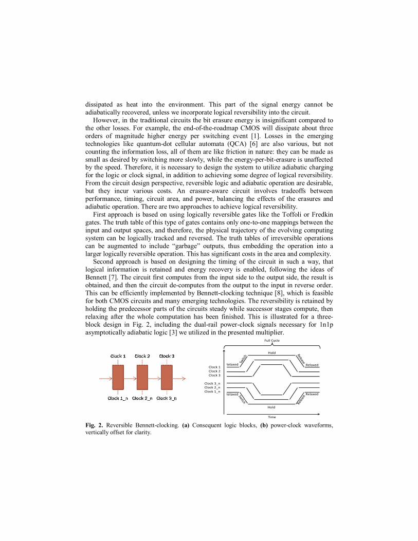
Second approach is based on designing the timing of the circuit in such a way, that logical information is retained and energy recovery is enabled, following the ideas of Bennett [7]. The circuit first computes from the input side to the output side, the result is obtained, and then the circuit de-computes from the output to the input in reverse order. This can be efficiently implemented by Bennett-clocking technique [8], which is feasible for both CMOS circuits and many emerging technologies. The reversibility is retained by holding the predecessor parts of the circuits steady while successor stages compute, then relaxing after the whole computation has been finished. This is illustrated for a three-block design in Fig. 2, including the dual-rail power-clock signals necessary for 1n1p asymptotically adiabatic logic [3] we utilized in the presented multiplier.
Fig. 2. Reversible Bennett-clocking. (a) Consequent logic blocks, (b) power-clock waveforms, vertically offset for clarity.

3 Combinatorial Multiplier
The designed 4-bit multiplier unit is based on a standard combinatorial structure laid out manually using CMOS transistors on a 2 µm technology node. The significant modifications are related to the static operating voltage and ground networks, which have been replaced with dynamic power-clock signals. These lines can be controlled to provide either static potentials for irreversible operation or ramped potentials for reversible Bennett-clocking. While the circuit has been fabricated on silicon, the measurements are currently work-in-progress, and we report only the simulation results.
Both modes of operation have been simulated in Synopsys HSPICE 2012, using a level 3 MOSFET model with parameters extracted from the devices made at the University of Notre Dame. The n-type transistors have a W/L ratio of 6 µm / 2µm with a threshold voltage of 0.7V, while the p-type transistors have a W/L ratio of 12 µm / 2 µm with a threshold voltage of -0.5V. The gate oxide thickness is 20nm.
3.1 Logical Structure and Implementation
The combinatorial structure of the standard multiplier unit is inherently logically irreversible, composing of standard CMOS logic gates and not utilizing any registers [9]. The unit takes as input two 4-bit words A = (A3, A2, A1, A0) and B = (B3, B2, B1, B0) and produces the 8-bit output word F = (F7,…, F0). The unsigned binary multiplication is defined if Fig. 3(a), while the grouping used for the addition of the summands AiBj in the implementation is depicted in Fig. 3(b), utilizing a Wallace tree arrangement for the addition of the slices of three-bit groups and a final two-operand carry-lookahead adder. The structure is shown in Fig. 4, consisting of 11 logic levels.
A3 A2 A1 A0
× B3 B2 B1 B0 A3B0 A2B0 A1B0 A0B0 A3B1 A2B1 A1B1 A0B1 A3B2 A2B2 A1B2 A0B2
+ A3B3 A2B3 A1B3 A0B3
F7 F6 F5 F4 F3 F2 F1 F0
Fig. 3. (a) 4-bit binary multiplication, and (b) grouping the summands AiBj and combining them with a Wallace adder tree and a final carry lookahead adder.
First stage
Second stage
Final stage

Fig. 4. Combinatorial multiplier based on Wallace tree summation and a final stage carry lookahead adder. The full adder (FA) units are used as half or full adders, depending on the location.
The design was laid out manually using a 2 µm CMOS technology, resulting in the fabricated layout shown in Fig.5. Instead of static operating voltage lines VDD and ground lines GND, we connected individual positive power-clocks Clk1…Clk11 to the pull-up side of the logic gates and negative power-clocks Clk1N…Clk11N to the pull-down side, effectively forming a programmable 11-stage pipeline. The control of the timing can be used to select irreversible or reversible operating mode.
3.2 Irreversible Operation
Like standard CMOS designs, the combinatorial multiplier unit can be run in irreversible mode by setting the power-clock lines to static values, which are held constant throughout the operation. The positive power-clocks Clk1…Clk11 are tied to the operating voltage VDD, while the negative power-clocks Clk1N…Clk11N are connected to ground GND. In this configuration, the unit implements a standard combinatorial CMOS multiplier, without pipelining or any sequential components. While the power-clocks virtually implement VDD and GND and are trivially simple to control, this mode of operation loses the logic signal energy exactly like traditional irreversible CMOS logic.
B0A0B0A1B1A0B0A2B1A1B2A0B0A3B1A2B2A1B3A0B1A3B2A2B3A1B2A3B3A2B3A3
VDDFAFA
FA
FAFAVDDFA
FAFAFAFA
4-Bit Carry Lookahead AdderA0B0A1B1A2B2A3B3
F0F1F2F3F4F5F6F7
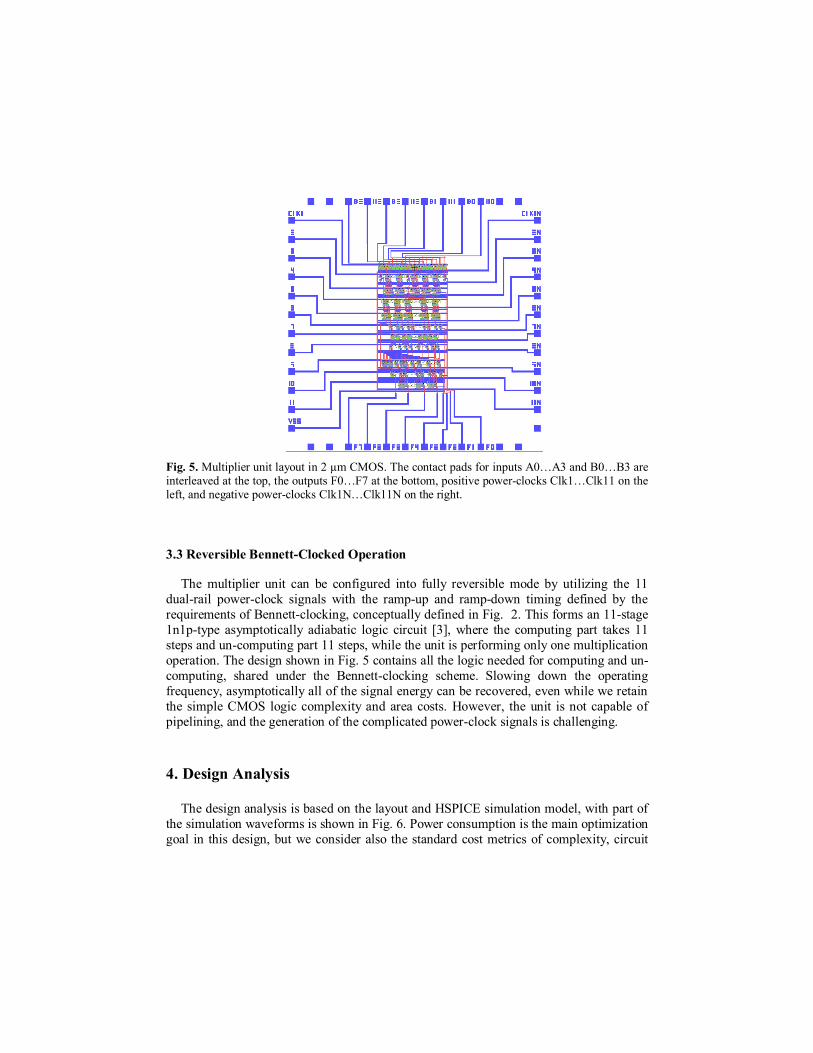
Fig. 5. Multiplier unit layout in 2 µm CMOS. The contact pads for inputs A0…A3 and B0…B3 are interleaved at the top, the outputs F0…F7 at the bottom, positive power-clocks Clk1…Clk11 on the left, and negative power-clocks Clk1N…Clk11N on the right.
3.3 Reversible Bennett-Clocked Operation
The multiplier unit can be configured into fully reversible mode by utilizing the 11 dual-rail power-clock signals with the ramp-up and ramp-down timing defined by the requirements of Bennett-clocking, conceptually defined in Fig. 2. This forms an 11-stage 1n1p-type asymptotically adiabatic logic circuit [3], where the computing part takes 11 steps and un-computing part 11 steps, while the unit is performing only one multiplication operation. The design shown in Fig. 5 contains all the logic needed for computing and un-computing, shared under the Bennett-clocking scheme. Slowing down the operating frequency, asymptotically all of the signal energy can be recovered, even while we retain the simple CMOS logic complexity and area costs. However, the unit is not capable of pipelining, and the generation of the complicated power-clock signals is challenging.
4. Design Analysis
The design analysis is based on the layout and HSPICE simulation model, with part of the simulation waveforms is shown in Fig. 6. Power consumption is the main optimization goal in this design, but we consider also the standard cost metrics of complexity, circuit

area, and performance in short. The logic complexity and area of the proposed multiplier core is practically equal to a static CMOS counterpart, if the circuitry required for generating the power-clocks is not considered. Determining this cost is ongoing work.
Fig. 6. Part of simulation output waveforms. (a) Irreversible operation with two signal levels and a voltage swing of 0—5 V. (b) Reversible operation with three signal levels and a voltage swing of
2.5—2.5 V. Only the outputs F0…F7 are shown.
The highest result throughput is dependent on the operating frequency, but it should be
noted that the irreversible combinatorial multiplier is limited by the longest signal path across the whole unit, while the reversible Bennett-clocked multiplier is divided into 11 stages, which each has an internal delay similar to a corresponding standard pipeline stage. The frequency limits for the multipliers are not equal, but generally, a small stage can be switched faster that the whole unit, while on the other hand, the adiabatic energy recovery is less with higher frequencies.
Power consumption of the multiplier was determined by averaging the results of HSPICE simulations in the range from 10 kHz to 1 GHz, shown in Fig. 7 as Watts vs. operating frequency. Irreversible mode has nearly two orders of magnitude higher power than the reversible from the slow end up to 1 MHz, while the modes get closer together from 20 or 30 MHz upwards, depending on the circuit parasitics. The irreversible multiplier is less affected by the parasitics than the reversible version, where the parasitic components clearly must be carefully controlled.

The designed layout is based on 2 µm CMOS, which is not ideal for the reversible multiplier. Based on preliminary work, moving to a 20 nm technology would raise the operating frequency by two orders magnitude, while the reversible design would surpass the irreversible up to a frequency of several GHz.
Fig. 7. Simulated average power consumption, irreversible vs. reversible operation. Including the paracitics extracted from the layout has adverse effects on both modes of operation, but more pronounced on the reversible operation.
5. Degree of Logical Reversibility
The Bennett-clocked multiplier is asymptotically adiabatic and recovers potentially nearly all of the signal energy, but with the cost of timing complexity. The combinatorial design itself is irreversible CMOS logic, which without the clocking approach both loses signal energy due to the static voltage operating principle and the bit erasures. In static CMOS, the energy loss due to losing logical information is insignificant compared to the total signal energy loss, however, adiabatic logic families and emerging technologies will benefit from avoiding the bit erasures in multiplication.
The amount of logical information loss in the standard irreversible multiplier can be estimated in a gate-level analysis, which gives a bound for the number of Landauer bit

erasures. While the inverter gates are logically reversible, even though a static CMOS implementation wastes all the signal energy, the other logic gates used in the design, NANDs and NORs, can be coarsely approximated to lose up to two bits of information each. With around 140 of these gates, we can expect 280 bit erasures per multiplication operation in this 4-bit structure. With growing word length, the complexity and the number of potential erasures scale according to a square-law.
Previous work on the theoretical binary multiplication operation indicates, that although the multiplication result value spectrum in Fig. 8 has a very complicated structure, it is possible to encode the logical relationship between the inputs and outputs uniquely with additional bits. The amount of extra bits scales linearly with the operand word length, and the theoretical minimum for full 4-bit multiplication is 5 erasures [10]. Therefore, multiplication should be amenable to modifications increasing the conservation of information and also the signal energy, even without Bennett-clocking. Currently, the authors are not aware of this type of developments having been published.
Fig. 8. Unsigned binary multiplication, the beginning of the result value spectrum for operand word lengths 2—8 bits. The trivial multiplication result zero has the maximum of occurrences for each word length, while the second-highest bars represent the highest non-trivial information loss.
6. Conclusion
Signal energy recovery enables high-efficiency computing, but has significant costs in circuit area, complexity, or timing. In this work, a configurable multiplier unit was designed and comparisons between irreversible and Bennett-clocked asymptotically adiabatic reversible mode conducted. With the simulated and prototyped 2 µm technology, the reversible operation was more efficient into the tens of MHz region. Based on expected scaling, the true benefits of adiabatic energy recovery will become

significant using more state-of-the-art 20 nm technology node. There the adiabatic operation would be orders of magnitude better up to GHz region.
The multiplier unit presented was not optimized for inherent logical reversibility, and therefore, Bennett-clocking is the only way to enable energy recovery. However, when examined on pure combinatorial logic level, it turns out that this kind of standard structure discards two orders of magnitude more information than the theoretical minimum of binary multiplication operation. This suggests that there is considerable potential to increase the degree of reversibility in the multiplier implementations without using the full Bennett embedding.
Currently, the analysis methods for the reversibility of circuit structures require development, as does the theoretical understanding of the connection between logical and physical reversibility. This area of research will likely become more and more important as the CMOS technology transitions to the limits of predicted physical scaling and beyond-CMOS technologies emerge. With transistor-less technologies utilizing charge-mode logic, the Landauer’s Principle and bit erasures will be significant design factors.
References
1. International Technology Roadmap for Semiconductors. (2009) ITRS report. [Online]. Available: http://www.itrs.net/Links/2009ITRS/Home2009.htm.
2. Starosel’skii, V.I.: Adiabatic Logic Circuits: A Review. Russian Microelectronics. Vol. 31, no. 1, pp. 37—58 (2002)
3. Valiev, K.A. and Starosel’skii, V.I.: A Model and Properties of a Thermodynamically Reversible Logic Gate. Russian Microelectronics. Vol. 29, no. 2, pp. 83–98 (2000)
4. Landauer, R.: Irreversibility and heat generation in the computing process. IBM J. Res. Dev. Vol. 5, pp. 183–191. Jul. (1961)
5. Berut, A, Arakelyan, A., Petrosyan, A., Ciliberto, S., Dillenschneider, R., and Lutz, E.: Experimental veri cation of Landauer’s principle linking information and thermodynamics. Nature. Vol. 483, pp. 187–189. Mar. (2012)
6. Lent, C. and Tougaw, P.: A device architecture for computing with quantum dots. Proc. IEEE. Vol. 85, no. 4, pp. 541–557. Apr. (1997)
7. Bennett, C.: Logical reversibility of computation. IBM J. Res. Dev. Vol. 17, pp. 525–532. Nov. (1973)
8. Lent, S., Liu, M., and Lu, Y.: Bennett clocking of quantum-dot cellular automata and the limits to binary logic scaling. Nanotechnology. Vol. 17, pp. 4240—4251. Aug. (2006)
9. Koren, I.: Computer Arithmetic Algorithms. 2nd ed. Natick, MA, USA: A. K. Peters, Ltd. (2002) 10.Hänninen, I., Takala, J., and Lent, C.: Irreversible bit erasures in binary multipliers. In: Proc.
IEEE Int. Symp. Circuits Syst., Rio de Janeiro, Brazil, May 15–18, pp. 2369–2372 (2011)