Embed Size (px)
Citation preview

Energy Scalable Reconfigurable CryptographicHardware for Portable Applications
by
James Ross Goodman
B. A.Sc. Electrical EngineeringUniversity of Waterloo, Waterloo, 1994
S.M. Electrical Engineering and Computer ScienceMassachusetts Institute of Technology, Cambridge, 1996
Submitted to the Department of Electrical Engineering and Computer Science
in partial fulfillment of the requirements for the Degree of
Doctor of Philosophy in Electrical Engineering and Computer Science
at the
MASSACHUSETTS INSTITUTE OF TECHNOLOGY
August 2000
2000 Massachusetts Institute of Technology. All rights reserved.
Signature of Author ________________________________________________Department of Electrical Engineering and Computer Science
September 11, 2000
Certified by ______________________________________________________Anantha Chandrakasan, Ph.D.
Associate Professor of Electrical EngineeringThesis Supervisor
Accepted by ______________________________________________________Arthur C. Smith, Ph.D.
Professor of Electrical EngineeringChairman, Department Committee on Graduate Students

2
3
Energy Scalable Reconfigurable CryptographicHardware for Portable Applications
by
James Ross Goodman
Submitted to the Department of Electrical Engineering and Computer Science
on September 11, 2000 in partial fulfillment of the requirements for the degree
of Doctor of Philosophy in Electrical Engineering and Computer Science
AbstractThe recent trends towards global networking and mobile computing have led to the proliferation ofwireless networks which enable users to remain connected to the global web without being tieddown to a fixed, wired link. The portable nature of these applications requires the development ofenergy-efficient hardware that is capable of providing a wide range of functionality in an energy-constrained environment that exhibits time-varying quality requirements. This work proposes uti-lizing an adaptive, energy-scalable approach that exposes the systems’ energy source to the hard-ware so that it can dynamically adjust its operating point in order to satisfy the current systemoperating requirements. Thus, the energy consumption of the system is based on the average-caseas opposed to the worst-case, leading to substantial improvements in the system’s operating life-time from a finite energy source. These results are verified through the development of an EnergyScalable Encryption Processor (ESEP) that features a high-efficiency embedded variable-outputpower converter. In addition, the lack of a coherent wireless network security architecture hasresulted in many different types of cryptographic primitives being used, requiring some form ofalgorithm agility in order to maximize the portable systems’ utility. Existing solutions are found tobe inadequate: software is flexible but energy-intensive, hardware is energy-efficient but not algo-rithm agile, and programmable logic incurs too much overhead to be considered energy-efficient.This work proposes a restricted form of reconfigurability, denoted domain-specific reconfigurabil-ity, that enables the required range of functionality (i.e., asymmetric cryptography) to be imple-mented without incurring the high overhead associated with conventional programmable logic-based solutions (e.g., FPGA’s). The benefits of this approach are verified through the developmentof the Domain Specific Reconfigurable Cryptographic Processor (DSRCP) which provides all ofthe flexibility of a software-based solution, while achieving, and in some instances surpassing, theenergy efficiency of a dedicated hardware-based solution in the domain of interest.
Thesis Supervisor: Anantha ChandrakasanTitle: Associate Professor of Electrical Engineering

4

5
Acknowledgements
First let me apologize in advance for what will surely seem to be a long-winded list of acknowledg-
ments. However, I truly feel that nothing in life can be accomplished without the help of others, and when
one reads another’s dissertation, a short list of acknowledgments only serves to betray the authors lack of
understanding of this fact. So buckle up because it’s going to be a long ride...
My deepest thanks go to my advisor Anantha Chandrakasan, who has always provided me with the
guidance, friendship, inspiration, resources, and most importantly, the intellectual freedom to pursue my
research here at MIT. Anantha’s kind spirit and good humour should serve as a guide to others on how to
deal with the often hard-facaded, fragile egos that are graduate students. I’ll always be indebted to him for
all that he’s done for me during my stay here in Boston. Thank you so very much for being such a fantastic
advisor and a good friend over these past 6 years.
I’d also like to thank the members of my thesis committee for agreeing to referee my dissertation. Tom
Knight (a.k.a., TK) was among the first people that I met here at MIT while visiting as a prospective stu-
dent, and to this day I’m still in awe of all he knows -- TK forgets more in a day than I’ll ever learn in a
lifetime. Prof. Anant Agarwal has always been a pleasure to interact with whether its discussing the energy
efficiency of the RAW architecture, or haggling over what constitutes a minor program here at MIT (Anant
had the dubious pleasure of being my academic advisor as well). Last, but definitely not least, I’d like to
thank Prof. Christof Paar from WPI, a kindred spirit who has served as a sounding board for my ideas on
hardware implementations of cryptographic algorithms, and who has become a good friend during the
course of my studies.
In addition, I’d also like to thank the rest of the MIT Faculty for providing me with an invaluable
knowledge base. In particular I’d like to thank Prof. Rivest for his encouragement and advice regarding all
things cryptologic -- his interest in the work that I had presented at my OQE single-handedly inspired me
to continue on with my research into cryptographic hardware.
Monica Bell and Marilyn Pierce deserve a very special thank you for helping me sort through all of the
admisitrivia of the graduate program, and for being so understanding when I would come to them, late as
usual, trying desperately to right some wrong that I had done. I’d argue that they’re the Department’s most
valuable resource, and I don’t think that you’ll find a dissenting opinion within the rest of the EECS gradu-
ate student community. Thank you both so very much for all of your help!

6
The work that this thesis describes is built upon a lot of help and insight that I’ve received over the
years from the member’s of Anantha’s group, as well as other students that I’ve interacted with over the
years. The Triumvirate of Pain (Duke Xanthopoulos, Raj Amirtharajah, and Tom Simon) deserve a special
thank you for their friendship and help over the years -- we started this group and chances are we’re going
to end it once they take a look at all of the havoc that we’ve wreaked! The rest of Anantha’s students, both
past and present, also deserve thanks for all that they’ve done for me over the years: Abram Dancy (a
model father, and a brilliant engineer whose DC/DC converter design skills enabled a great deal of my
research to occur), Tom Barber (whose competitiveness will eventually lead me to an early grave... it’s
tough keeping up with you big guy!), Vadim Gutnik (we all know he chose Austin because it lets him keep
up the Berkeley tradition of wearing shorts all year long without enduring the frostbite of Boston...),
Debashis Saha (loyal patron of the Kresge Lot clubbing scene), Gangadar Konduri (who still hasn’t
explained to me why cricket games take several days, but who could probably catch a bullet with his bare
hands if he ever tries...), Amit (“bad boy to the stars”) Sinha, SeongHwan Cho (get out now while you still
can!), Alice Wang (whom I TAed during my first year at MIT, and who is now a fellow Ph.D. candidate...
talk about a sign that you need to graduate!), Wendi Rabiner (still the wisest among us for not doing hard-
ware), Rex Min (who, despite his rantings, is anything but old...), and last (and definitely least!) Manish
Bhardwaj who reminds me so much of myself (without the stunning good looks of course...) that it’s scary.
Outside of the group I’ve also had the distinct pleasure of knowing Dan McMahill and Don Hitko, who just
might be the only two guys at MIT who love hockey more than myself! Thanks as well to all of Charlie’s
and Harry’s graduate students who have been so very patient answering all of my circuit questions over the
years.
A special thank you is also owed to our administrative assistants Beth Cheung and Margaret Flaherty.
These ladies are the sole reason that anything actually gets done around here! I don’t know how I would
have managed without their sagely advice for dealing with MIT’s bureaucracy and administrivia. As if that
weren’t enough, they also happen to be wonderful people that were a joy to be around. Thank you both so
very much!
Undoubtedly the most enjoyable aspect of my tenure here at MIT has been the time that I’ve spent
playing hockey with the MIT Varsity Hockey Team. Where else can someone start playing competitive
hockey again at the age of 24, after a 6 year hiatus?! My time with the team has served as a valuable stress
release, and a source of many of my close friends here at MIT. I’ll never forget the lessons that I’ve learned
from the likes of Coach Bill (“Give him a little how-do-you-do and get off the ice...”) and Coach Quinn
(“I’m strong on my stick - you can’t push me over...”), or the fun that I’ve had playing under the O’Meara

7
boys (Mark, Jimmy, and Froggy). Thanks to all those that have made playing hockey such fun: Buddy, Z,
Rae (dynasty baby!), Tetsu, Schlootz, Thorson, Yurk, Goon, Woodsy, Splash, Russ, JD, Benoit, Capper,
Shane-o, Rocky (my bad!), Martin the dancing Swede, Hynesy, and Dage.
Two people that deserve special consideration are the gentlemen that initially started me on my jour-
ney through academia that has led me here: Robert Leperre and Duncan MacDonald. Without their encour-
agement and guidance I never would have gone to Waterloo, which means that I probably would never
have gone to MIT. I don’t know if I’ve ever thanked them for that initial nudge, but if not, then I’d like to
now. Thank you both so very much.
Once at Waterloo I had the good fortune to be introduced to several professors who became role mod-
els for me. Once I saw just how profound a positive effect they could have on students I knew that I wanted
the opportunity to do the same. Thanks to professors Vannelli and Wang for showing that in this increas-
ingly narcissistic society, some people are still capable of caring deeply for others and providing a fantastic
opportunity to learn.
Of course, we’re all nothing without the love and support of our families and thankfully I have one of
the most loving, caring, and understanding family of them all. My sister Lisa, her husband Cory, and my
newly-arrived niece Kate have always been there for both my wife and I over the years -- there constant
love and affection were most welcome during the rougher parts of my stay. My step-father Milt has
remained the gentleman he always was, and a man whom I respect very deeply. Sadly I can’t share this
with my mother Kate -- a woman who knew no equal when it came to motherhood. I miss her deeply and
only wish that she could share in this with me -- it’s as much her accomplishment as it is mine. I love you
and miss you dearly. Back home I’ve also had the loving support of my many relatives and in particular
Oma & Opa, Nannie, Cuttie, Andrew & Marilyn, Nellie & Peter, and Debbie & Howard. The love that
they’ve shown me over the years has always been unending and unconditional. Thank you all so very
much. In addition, I’ve managed to pick up another family during my stay here in Boston! My lovely
wife’s family has treated me with all the love and kindness that anyone could ask for and for that I’d like to
thank them all from the very bottom of my heart. Thank you Mike, Voula, Maria, Tasso, and Touly - it’s an
honour to call you all my family.
Of course, as most who know me here at MIT will attest, I’m only half of the whole - a partner in
crime along with Mr. Anthony “Grandpa” Gray. I met Tony during my first term here at MIT playing
hockey (surprise, surprise!) and MIT has suffered greatly ever since - he’s the brother I never had but

8
always wanted. The fact that I’ve managed to keep my wits during my tenure here at MIT can
largely be attributed to Tony’s constant friendship, good humour, and caring nature, properties that
he’s inherited from his loving parents and family. He’s the best friend that a person could ever ask
for. Thank you for all that you’ve done Grandpa, I don’t know what I would have done without you
and your family.
The last person that I’d like to thank is the one who means the most to me. My lovely wife
Smaragda has endured many lonely nights and uneventful evenings as I’ve burned the midnight oil
in pursuit of my Ph.D. Truth be known, I don’t know where to begin thanking her for all that she’s
done, from reading thesis drafts, to taking care of absolutely everything in our lives outside of
school and providing almost constant moral support and encouragement during the last, very long
haul. The depth of her love and support has always amazed me, I only hope that I can now in some
small way begin to pay her back for all of her patience and encouragement -- thankfully I’ve got a
lifetime to do it! I love you so very much Smag, thank you from the very bottom of my heart for all
that you’ve done. You’re simply the greatest thing that ever happened to me...

9
The sun was now just above the tallest spires, and the flooding light that turnedthe dusty pavement to red gold made me feel philosophical. In the brown book inmy sabretache there was the tale of an angel (perhaps one of the winged womenwarriors who are said to serve the Autarch) who, coming to Urth on some pettymission or other, was struck by a child’s arrow and died. With her gleaming robesall dyed by her heart’s blood, even as the boulevards were stained by the expiringlife of the sun, she encountered Gabriel himself. His sword blazed in one hand, hisgreat two-headed axe swung in the other, and across his back, suspended on therainbow, hung the very battle horn of Heaven.
“Where wend you, little one,” asked Gabriel, “with your breast more scarlet thanthe robin’s?”
“I am killed,” the angel said, “and I return to merge my substance once more withthe Pancreator.”
“Do not be absurd. You are an angel, a pure spirit, and cannot die.”
“But I am dead,” said the angel, “nevertheless. You have observed the wasting ofmy blood -- do you not observe also that it no longer issues in straining spurtings,but only seeps sluggishly? Note the pallor of my countenance. Is not the touch ofan angel warm and bright? Take my hand and you will imagine you hold a horrornew dragged from some stagnant pool. Taste my breath -- is it not fetid, foul, andnidorous?” Gabriel answered nothing, and at last the angel said, “Brother andbetter, even if I have not convinced you with all my proofs, I pray you stand aside.I would rid the universe of my presence.”
“I am convinced indeed,” Gabriel said, stepping from the other’s way. “It is onlythat I was thinking that had I known we might perish, I would not at all times havebeen so bold.”
- Shadow of the Torturer by Gene Wolfe

10

11
Table of Contents
1 Introduction 29
1.1 Introduction to Cryptography . . . . . . . . . . . . . . . . . . . . . . . . . . . . . . . . . . . . . . . . . . . . 331.1.1 A Simple Example . . . . . . . . . . . . . . . . . . . . . . . . . . . . . . . . . . . . . . . . . . . . . . 331.1.2 Secret Key Algorithm Types . . . . . . . . . . . . . . . . . . . . . . . . . . . . . . . . . . . . . . 371.1.3 Public Key Algorithm Types . . . . . . . . . . . . . . . . . . . . . . . . . . . . . . . . . . . . . . 371.1.4 Security Estimates for Asymmetric Cryptographic Algorithms. . . . . . . . . . . . 38
1.2 Previous Work . . . . . . . . . . . . . . . . . . . . . . . . . . . . . . . . . . . . . . . . . . . . . . . . . . . . . . . 381.2.1 Low Power and Energy Efficient CMOS Design. . . . . . . . . . . . . . . . . . . . . . . 381.2.2 Energy Efficient Reconfigurable Architectures . . . . . . . . . . . . . . . . . . . . . . . . 391.2.3 Public Key Cryptographic Software. . . . . . . . . . . . . . . . . . . . . . . . . . . . . . . . . 391.2.4 Public Key Cryptographic Hardware . . . . . . . . . . . . . . . . . . . . . . . . . . . . . . . . 40
1.3 Thesis Overview and Contributions . . . . . . . . . . . . . . . . . . . . . . . . . . . . . . . . . . . . . . . 42
2 A Primer in Number Theory and Elliptic Curves 45
2.1 Groups, Rings, and Fields . . . . . . . . . . . . . . . . . . . . . . . . . . . . . . . . . . . . . . . . . . . . . . . 452.1.1 Field Polynomials and Extension Fields . . . . . . . . . . . . . . . . . . . . . . . . . . . . . 472.1.2 Composite Fields . . . . . . . . . . . . . . . . . . . . . . . . . . . . . . . . . . . . . . . . . . . . . . . 472.1.3 Basis Representation. . . . . . . . . . . . . . . . . . . . . . . . . . . . . . . . . . . . . . . . . . . . . 48
2.2 Elliptic Curves . . . . . . . . . . . . . . . . . . . . . . . . . . . . . . . . . . . . . . . . . . . . . . . . . . . . . . . 492.2.1 Affine vs. Projective Co-ordinates . . . . . . . . . . . . . . . . . . . . . . . . . . . . . . . . . . 492.2.2 Supersingular vs. Non-supersingular Elliptic Curves. . . . . . . . . . . . . . . . . . . . 512.2.3 Point Addition and Doubling . . . . . . . . . . . . . . . . . . . . . . . . . . . . . . . . . . . . . . 512.2.4 Point Order . . . . . . . . . . . . . . . . . . . . . . . . . . . . . . . . . . . . . . . . . . . . . . . . . . . . 55
3 Software Implementations of Public Key Cryptographic Algorithms 57
3.1 Multi-precision Arithmetic . . . . . . . . . . . . . . . . . . . . . . . . . . . . . . . . . . . . . . . . . . . . . . 57
3.2 Assembly Language vs. C-Based Software Implementations . . . . . . . . . . . . . . . . . . . 59
3.3 Experimental Setup . . . . . . . . . . . . . . . . . . . . . . . . . . . . . . . . . . . . . . . . . . . . . . . . . . . . 59
3.4 Multi-precision Modular Integer Arithmetic . . . . . . . . . . . . . . . . . . . . . . . . . . . . . . . . 613.4.1 Notation . . . . . . . . . . . . . . . . . . . . . . . . . . . . . . . . . . . . . . . . . . . . . . . . . . . . . . 623.4.2 Addition/Subtraction . . . . . . . . . . . . . . . . . . . . . . . . . . . . . . . . . . . . . . . . . . . . 62
12
3.4.3 Integer Multiplication and Squaring. . . . . . . . . . . . . . . . . . . . . . . . . . . . . . . . . 643.4.3.1 The Karatsuba-Ofman Algorithm . . . . . . . . . . . . . . . . . . . . . . . . . . 653.4.3.2 Comba’s Method . . . . . . . . . . . . . . . . . . . . . . . . . . . . . . . . . . . . . . . 673.4.3.3 Fast Fourier Transform (FFT) Based Multiplication . . . . . . . . . . . . 68
3.4.4 Integer Division . . . . . . . . . . . . . . . . . . . . . . . . . . . . . . . . . . . . . . . . . . . . . . . . 683.4.5 Modular Reduction and Montgomery’s Method . . . . . . . . . . . . . . . . . . . . . . . 693.4.6 Modular Multiplication and Squaring . . . . . . . . . . . . . . . . . . . . . . . . . . . . . . . 723.4.7 Modular Exponentiation . . . . . . . . . . . . . . . . . . . . . . . . . . . . . . . . . . . . . . . . . . 74
3.4.7.1 Chinese Remainder Theorem. . . . . . . . . . . . . . . . . . . . . . . . . . . . . . 76
3.5 Galois Field Arithmetic . . . . . . . . . . . . . . . . . . . . . . . . . . . . . . . . . . . . . . . . . . . . . . . . 763.5.1 Notation . . . . . . . . . . . . . . . . . . . . . . . . . . . . . . . . . . . . . . . . . . . . . . . . . . . . . . 773.5.2 Field-Specific vs. Composite Fields vs. Generic GF(2n) Implementations . . . 783.5.3 GF(2n) Addition/Subtraction . . . . . . . . . . . . . . . . . . . . . . . . . . . . . . . . . . . . . . 783.5.4 GF(2n) Multiplication . . . . . . . . . . . . . . . . . . . . . . . . . . . . . . . . . . . . . . . . . . . . 793.5.5 GF(2n) Squaring . . . . . . . . . . . . . . . . . . . . . . . . . . . . . . . . . . . . . . . . . . . . . . . . 803.5.6 GF(2n) Inversion. . . . . . . . . . . . . . . . . . . . . . . . . . . . . . . . . . . . . . . . . . . . . . . . 823.5.7 GF(2n) Exponentiation . . . . . . . . . . . . . . . . . . . . . . . . . . . . . . . . . . . . . . . . . . . 84
3.6 Elliptic Curve Arithmetic . . . . . . . . . . . . . . . . . . . . . . . . . . . . . . . . . . . . . . . . . . . . . . . 843.6.1 Point Addition and Doubling . . . . . . . . . . . . . . . . . . . . . . . . . . . . . . . . . . . . . . 843.6.2 Point Multiplication . . . . . . . . . . . . . . . . . . . . . . . . . . . . . . . . . . . . . . . . . . . . . 84
3.7 Energy Efficiency of Software-based Asymmetric Cryptography . . . . . . . . . . . . . . . . 873.7.1 Comparison of IF, DL, and EC-based Software Energy Efficiencies . . . . . . . 883.7.2 Energy Scalable Software. . . . . . . . . . . . . . . . . . . . . . . . . . . . . . . . . . . . . . . . . 89
3.8 Hardware Architectural Considerations for Software Solutions . . . . . . . . . . . . . . . . . 91
3.9 Summary of Contributions . . . . . . . . . . . . . . . . . . . . . . . . . . . . . . . . . . . . . . . . . . . . . . 94
4 Energy Scalable Encryption Processor (ESEP) 97
4.1 Definition of Energy Scalability . . . . . . . . . . . . . . . . . . . . . . . . . . . . . . . . . . . . . . . . . . 97
4.2 Quadratic Residue Generator (QRG) . . . . . . . . . . . . . . . . . . . . . . . . . . . . . . . . . . . . . . 994.2.1 Modular Multiplication Algorithm. . . . . . . . . . . . . . . . . . . . . . . . . . . . . . . . . 100
4.3 An Energy Scalable Processor Architecture . . . . . . . . . . . . . . . . . . . . . . . . . . . . . . . . 1034.3.1 Global Sequencer . . . . . . . . . . . . . . . . . . . . . . . . . . . . . . . . . . . . . . . . . . . . . . 1054.3.2 Output Selector and Converter . . . . . . . . . . . . . . . . . . . . . . . . . . . . . . . . . . . . 1064.3.3 High Efficiency Embedded Power Supply . . . . . . . . . . . . . . . . . . . . . . . . . . . 108
4.4 Energy Reduction Techniques . . . . . . . . . . . . . . . . . . . . . . . . . . . . . . . . . . . . . . . . . . 1094.4.1 Concurrency Driven Voltage Scaling. . . . . . . . . . . . . . . . . . . . . . . . . . . . . . . 1094.4.2 Self-timed Gating . . . . . . . . . . . . . . . . . . . . . . . . . . . . . . . . . . . . . . . . . . . . . . 1104.4.3 Clock Gating and Shutdown. . . . . . . . . . . . . . . . . . . . . . . . . . . . . . . . . . . . . . 111
4.5 Implementation . . . . . . . . . . . . . . . . . . . . . . . . . . . . . . . . . . . . . . . . . . . . . . . . . . . . . . 1134.5.1 Processing Bitslice . . . . . . . . . . . . . . . . . . . . . . . . . . . . . . . . . . . . . . . . . . . . . 114
13
4.5.1.1 X Selector . . . . . . . . . . . . . . . . . . . . . . . . . . . . . . . . . . . . . . . . . . . . 1154.5.1.2 Redundant Adder #1. . . . . . . . . . . . . . . . . . . . . . . . . . . . . . . . . . . . 1164.5.1.3 N Selector . . . . . . . . . . . . . . . . . . . . . . . . . . . . . . . . . . . . . . . . . . . . 1164.5.1.4 Redundant Adder #2. . . . . . . . . . . . . . . . . . . . . . . . . . . . . . . . . . . . 117
4.5.2 Output Selector and Converter . . . . . . . . . . . . . . . . . . . . . . . . . . . . . . . . . . . . 1174.5.3 Quotient Estimate Unit . . . . . . . . . . . . . . . . . . . . . . . . . . . . . . . . . . . . . . . . . . 1184.5.4 Y Recoder . . . . . . . . . . . . . . . . . . . . . . . . . . . . . . . . . . . . . . . . . . . . . . . . . . . . 1204.5.5 Controller Logic . . . . . . . . . . . . . . . . . . . . . . . . . . . . . . . . . . . . . . . . . . . . . . . 1214.5.6 Variable Output DC/DC Converter . . . . . . . . . . . . . . . . . . . . . . . . . . . . . . . . 121
4.6 Verification . . . . . . . . . . . . . . . . . . . . . . . . . . . . . . . . . . . . . . . . . . . . . . . . . . . . . . . . . 124
4.7 Experimental Results . . . . . . . . . . . . . . . . . . . . . . . . . . . . . . . . . . . . . . . . . . . . . . . . . 1254.7.1 Energy Scalability. . . . . . . . . . . . . . . . . . . . . . . . . . . . . . . . . . . . . . . . . . . . . . 1254.7.2 Power Supply Efficiency and Settling Time . . . . . . . . . . . . . . . . . . . . . . . . . 1274.7.3 Hardware vs. Software Efficiency . . . . . . . . . . . . . . . . . . . . . . . . . . . . . . . . . 129
4.8 Summary of Contributions . . . . . . . . . . . . . . . . . . . . . . . . . . . . . . . . . . . . . . . . . . . . . 130
5 Domain Specific Reconfigurable Cryptographic Processor (DSRCP) 133
5.1 IEEE Public Key Cryptography Standard (P1363) . . . . . . . . . . . . . . . . . . . . . . . . . . 1345.1.1 Discrete Logarithm (DL) . . . . . . . . . . . . . . . . . . . . . . . . . . . . . . . . . . . . . . . . 1355.1.2 Integer Factorization (IF) . . . . . . . . . . . . . . . . . . . . . . . . . . . . . . . . . . . . . . . . 1365.1.3 Elliptic Curve Discrete Logarithm (ECDL) . . . . . . . . . . . . . . . . . . . . . . . . . . 137
5.2 Programmable Logic and Domain Specific Reconfigurability . . . . . . . . . . . . . . . . . 138
5.3 Instruction Set Definition/Architecture . . . . . . . . . . . . . . . . . . . . . . . . . . . . . . . . . . . 1395.3.1 DSRCP Instruction Set . . . . . . . . . . . . . . . . . . . . . . . . . . . . . . . . . . . . . . . . . . 140
5.4 Architecture . . . . . . . . . . . . . . . . . . . . . . . . . . . . . . . . . . . . . . . . . . . . . . . . . . . . . . . . 1415.4.1 Controller and Microcode ROMs . . . . . . . . . . . . . . . . . . . . . . . . . . . . . . . . . . 1425.4.2 Shutdown Controller. . . . . . . . . . . . . . . . . . . . . . . . . . . . . . . . . . . . . . . . . . . . 1435.4.3 I/O Interface . . . . . . . . . . . . . . . . . . . . . . . . . . . . . . . . . . . . . . . . . . . . . . . . . . 1445.4.4 Reconfigurable Datapath . . . . . . . . . . . . . . . . . . . . . . . . . . . . . . . . . . . . . . . . 144
5.5 Algorithm Implementation . . . . . . . . . . . . . . . . . . . . . . . . . . . . . . . . . . . . . . . . . . . . . 1465.5.1 Conventional Multiplication. . . . . . . . . . . . . . . . . . . . . . . . . . . . . . . . . . . . . . 1475.5.2 Modular Addition/Subtraction . . . . . . . . . . . . . . . . . . . . . . . . . . . . . . . . . . . . 1475.5.3 Montgomery Reduction . . . . . . . . . . . . . . . . . . . . . . . . . . . . . . . . . . . . . . . . . 1485.5.4 Modular Reduction . . . . . . . . . . . . . . . . . . . . . . . . . . . . . . . . . . . . . . . . . . . . . 1485.5.5 Modular Multiplication. . . . . . . . . . . . . . . . . . . . . . . . . . . . . . . . . . . . . . . . . . 1495.5.6 Modular Inversion . . . . . . . . . . . . . . . . . . . . . . . . . . . . . . . . . . . . . . . . . . . . . 1495.5.7 Modular Exponentiation . . . . . . . . . . . . . . . . . . . . . . . . . . . . . . . . . . . . . . . . . 149
5.5.7.1 Timing Attacks. . . . . . . . . . . . . . . . . . . . . . . . . . . . . . . . . . . . . . . . 1505.5.8 GF(2n) Inversion. . . . . . . . . . . . . . . . . . . . . . . . . . . . . . . . . . . . . . . . . . . . . . . 1525.5.9 GF(2n) Addition/Subtraction . . . . . . . . . . . . . . . . . . . . . . . . . . . . . . . . . . . . . 1525.5.10 GF(2n) Multiplication . . . . . . . . . . . . . . . . . . . . . . . . . . . . . . . . . . . . . . . . . . . 152
14
5.5.11 GF(2n) Exponentiation . . . . . . . . . . . . . . . . . . . . . . . . . . . . . . . . . . . . . . . . . . 1525.5.12 Elliptic Curve Point Doubling . . . . . . . . . . . . . . . . . . . . . . . . . . . . . . . . . . . . 1525.5.13 Elliptic Curve Point Addition . . . . . . . . . . . . . . . . . . . . . . . . . . . . . . . . . . . . . 1545.5.14 Elliptic Curve Point Multiplication . . . . . . . . . . . . . . . . . . . . . . . . . . . . . . . . 154
5.6 Reconfigurable Processing Element Design . . . . . . . . . . . . . . . . . . . . . . . . . . . . . . . . 1565.6.1 Register File . . . . . . . . . . . . . . . . . . . . . . . . . . . . . . . . . . . . . . . . . . . . . . . . . . 1565.6.2 I/O Interface . . . . . . . . . . . . . . . . . . . . . . . . . . . . . . . . . . . . . . . . . . . . . . . . . . 1575.6.3 Magnitude Comparator. . . . . . . . . . . . . . . . . . . . . . . . . . . . . . . . . . . . . . . . . . 1585.6.4 Carry Bypass Add/Subtract Unit . . . . . . . . . . . . . . . . . . . . . . . . . . . . . . . . . . 1585.6.5 Reconfigurable Datapath . . . . . . . . . . . . . . . . . . . . . . . . . . . . . . . . . . . . . . . . 160
5.6.5.1 Montgomery Multiplication and Reduction. . . . . . . . . . . . . . . . . . 1615.6.5.2 GF(2n) Multiplication. . . . . . . . . . . . . . . . . . . . . . . . . . . . . . . . . . . 1625.6.5.3 GF(2n) Inversion . . . . . . . . . . . . . . . . . . . . . . . . . . . . . . . . . . . . . . 1645.6.5.4 Redundant Number Representation . . . . . . . . . . . . . . . . . . . . . . . . 1665.6.5.5 Final Datapath Cell Design . . . . . . . . . . . . . . . . . . . . . . . . . . . . . . 168
5.7 Implementation . . . . . . . . . . . . . . . . . . . . . . . . . . . . . . . . . . . . . . . . . . . . . . . . . . . . . . 1695.7.1 Controller and Microcode ROMs . . . . . . . . . . . . . . . . . . . . . . . . . . . . . . . . . . 1705.7.2 Shutdown Controller. . . . . . . . . . . . . . . . . . . . . . . . . . . . . . . . . . . . . . . . . . . . 1715.7.3 I/O Interface . . . . . . . . . . . . . . . . . . . . . . . . . . . . . . . . . . . . . . . . . . . . . . . . . . 1725.7.4 Reconfigurable Datapath Bitslice . . . . . . . . . . . . . . . . . . . . . . . . . . . . . . . . . . 174
5.7.4.1 I/O Cell . . . . . . . . . . . . . . . . . . . . . . . . . . . . . . . . . . . . . . . . . . . . . . 1775.7.4.2 Register File . . . . . . . . . . . . . . . . . . . . . . . . . . . . . . . . . . . . . . . . . . 1775.7.4.3 Comparator Unit. . . . . . . . . . . . . . . . . . . . . . . . . . . . . . . . . . . . . . . 1785.7.4.4 Adder Unit . . . . . . . . . . . . . . . . . . . . . . . . . . . . . . . . . . . . . . . . . . . 1795.7.4.5 Reconfigurable Datapath . . . . . . . . . . . . . . . . . . . . . . . . . . . . . . . . 180
5.7.5 SHA-1 Hash Function Engine . . . . . . . . . . . . . . . . . . . . . . . . . . . . . . . . . . . . 182
5.8 Verification . . . . . . . . . . . . . . . . . . . . . . . . . . . . . . . . . . . . . . . . . . . . . . . . . . . . . . . . . 1855.8.1 DSRCP Test Board. . . . . . . . . . . . . . . . . . . . . . . . . . . . . . . . . . . . . . . . . . . . . 187
5.9 Experimental Results . . . . . . . . . . . . . . . . . . . . . . . . . . . . . . . . . . . . . . . . . . . . . . . . . 1885.9.1 Comparison to Conventional Software and FPGA-based Solutions . . . . . . . 191
5.10 Summary of Contributions . . . . . . . . . . . . . . . . . . . . . . . . . . . . . . . . . . . . . . . . . . . . . 194
6 Conclusions 197
6.1 Summary of Contributions . . . . . . . . . . . . . . . . . . . . . . . . . . . . . . . . . . . . . . . . . . . . . 198
6.2 Future Work . . . . . . . . . . . . . . . . . . . . . . . . . . . . . . . . . . . . . . . . . . . . . . . . . . . . . . . . 199
References 203
Appendix A Energy Scalable Encryption Processor User’s Manual 213
15
A.1 Pin Descriptions. . . . . . . . . . . . . . . . . . . . . . . . . . . . . . . . . . . . . . . . . . . . . . . . . . . . . . 214
A.2 Package Diagrams . . . . . . . . . . . . . . . . . . . . . . . . . . . . . . . . . . . . . . . . . . . . . . . . . . . . 215
A.3 Determining Clock Rate and Supply Voltage . . . . . . . . . . . . . . . . . . . . . . . . . . . . . . . 216
A.4 Basic Operation . . . . . . . . . . . . . . . . . . . . . . . . . . . . . . . . . . . . . . . . . . . . . . . . . . . . . . 218A.4.1 Initialization . . . . . . . . . . . . . . . . . . . . . . . . . . . . . . . . . . . . . . . . . . . . . . . . . . 218A.4.2 Multiplication . . . . . . . . . . . . . . . . . . . . . . . . . . . . . . . . . . . . . . . . . . . . . . . . . 219
A.5 Embedded DC/DC Converter . . . . . . . . . . . . . . . . . . . . . . . . . . . . . . . . . . . . . . . . . . . 220A.5.1 Single-wire Serial Interface . . . . . . . . . . . . . . . . . . . . . . . . . . . . . . . . . . . . . . 220A.5.2 Configuring the DC/DC Converter. . . . . . . . . . . . . . . . . . . . . . . . . . . . . . . . . 221
Appendix B DSRCP Instruction Set Definition 225
B.1 Detailed Instruction Descriptions . . . . . . . . . . . . . . . . . . . . . . . . . . . . . . . . . . . . . . . . 226
Appendix C DSRCP User’s Manual 235
C.1 Pin Descriptions. . . . . . . . . . . . . . . . . . . . . . . . . . . . . . . . . . . . . . . . . . . . . . . . . . . . . . 236
C.2 Package Diagrams . . . . . . . . . . . . . . . . . . . . . . . . . . . . . . . . . . . . . . . . . . . . . . . . . . . . 237
C.3 Basic Operation . . . . . . . . . . . . . . . . . . . . . . . . . . . . . . . . . . . . . . . . . . . . . . . . . . . . . . 238C.3.1 Data Transfer to/from the DSRCP . . . . . . . . . . . . . . . . . . . . . . . . . . . . . . . . . 239
Appendix D SHA-1 Circuit Schematics 241
D.1 Complete SHA-1 Circuit Schematics . . . . . . . . . . . . . . . . . . . . . . . . . . . . . . . . . . . . . 242

16

17
List of Figures
1-1 Estimates of the number of wired and wireless network users. . . . . . . . . . . . . . . . . . 29
1-2 Estimates of the number of wired and wireless network users. . . . . . . . . . . . . . . . . . 30
1-3 Survey results for determining barriers that prevent people from usingthe Internet for retail commerce. . . . . . . . . . . . . . . . . . . . . . . . . . . . . . . . . . . . . . . . . . 31
1-4 Alice and Bob trying to conduct a private conversation over wirelesschannels and failing miserably as Eve listens in. . . . . . . . . . . . . . . . . . . . . . . . . . . . . 34
1-5 Alice and Bob using cryptography to encode their communications. . . . . . . . . . . . . . 36
2-1 Graphical interpretation of elliptic curve point (a) addition, (b) doubling. . . . . . . . . . 52
3-1 Multi-precision mapping of n-bit integers to a w-bit processingarchitecture using base-2k representation. . . . . . . . . . . . . . . . . . . . . . . . . . . . . . . . . . . 58
3-2 Multi-precision mapping of n-bit elements of GF(2n) to a w-bitprocessing architecture. . . . . . . . . . . . . . . . . . . . . . . . . . . . . . . . . . . . . . . . . . . . . . . . . 59
3-3 StrongARM SA-1100 “Brutus” evaluation platform. . . . . . . . . . . . . . . . . . . . . . . . . . 60
3-4 Multi-precision multiplication/squaring examples. . . . . . . . . . . . . . . . . . . . . . . . . . . . 64
3-5 Comparison of conventional multiplication with Comba’s method. . . . . . . . . . . . . . 67
3-6 Conventional multi-precision integer division example. . . . . . . . . . . . . . . . . . . . . . . 69
3-7 Example reduction over GF(210). . . . . . . . . . . . . . . . . . . . . . . . . . . . . . . . . . . . . . . . . 80
3-8 Comparison of GF(2n) multiplication to both conventional andMontgomery modular multiplication. . . . . . . . . . . . . . . . . . . . . . . . . . . . . . . . . . . . . . 81
3-9 Example squaring over GF(24). . . . . . . . . . . . . . . . . . . . . . . . . . . . . . . . . . . . . . . . . . . 81
3-10 LUT-based squaring operation w/o reduction step. . . . . . . . . . . . . . . . . . . . . . . . . . . 81
3-11 Comparison of EC and IF/DL based software implementations. . . . . . . . . . . . . . . . . 89
3-12 Minimum supply voltage vs. clock frequency of the StrongARM SA-1100. . . . . . . . 90
3-13 Average energy consumption per cycle of operation of the StrongARMSA-1100 as a function of the clock frequency and supply voltage . . . . . . . . . . . . . . . 90
3-14 Hardware-enabled performance improvement over conventional approaches. . . . . . 92
3-15 Modification to booth-recoding for GF(2n) multiplication cell anddecoder using existing booth-recoded integer multiplier. . . . . . . . . . . . . . . . . . . . . . . 93

18
3-16 Comparison of conventional, and gated carry-out adder cell performance. . . . . . . . . 93
3-17 Gated carry-out adder cell schematic. . . . . . . . . . . . . . . . . . . . . . . . . . . . . . . . . . . . . . 94
4-1 Fixed vs. energy-scalable implementations as a function of normalized workload. . . 98
4-2 Normalized encryption energy consumption per compressed videoframe for two image sequences. . . . . . . . . . . . . . . . . . . . . . . . . . . . . . . . . . . . . . . . . . 99
4-3 Estimated amount of computation required to factor n-bit moduli. . . . . . . . . . . . . . 100
4-4 Modular multiplication algorithm block diagram. . . . . . . . . . . . . . . . . . . . . . . . . . . 102
4-5 Overall system architecture of the ESEP. . . . . . . . . . . . . . . . . . . . . . . . . . . . . . . . . . 103
4-6 Top-level architecture of the encryption engine (QRG). . . . . . . . . . . . . . . . . . . . . . . 105
4-7 Tree-based comparator circuit for determining sign of result in QRG. . . . . . . . . . . 107
4-8 Output converter circuit. . . . . . . . . . . . . . . . . . . . . . . . . . . . . . . . . . . . . . . . . . . . . . . 108
4-9 Top level ESEP DC/DC converter architecture. . . . . . . . . . . . . . . . . . . . . . . . . . . . . 108
4-10 Pipelining the Y operand recoder unit to reduce the critical path. . . . . . . . . . . . . . . 109
4-11 Optimizing and parallelizing the quotient estimation unit to reduce critical path. . . 110
4-12 Block diagram of the self-timed gating of the datapath. . . . . . . . . . . . . . . . . . . . . . . 111
4-13 Switch capacitance reduction of the Y operand shift register. . . . . . . . . . . . . . . . . . 111
4-14 Normalized switched capacitance of the Y operand shift register as afunction of the amount of register segmentation. . . . . . . . . . . . . . . . . . . . . . . . . . . . 112
4-15 Die photograph of the ESEP. . . . . . . . . . . . . . . . . . . . . . . . . . . . . . . . . . . . . . . . . . . 113
4-16 QRG bitslice architecture. . . . . . . . . . . . . . . . . . . . . . . . . . . . . . . . . . . . . . . . . . . . . . 114
4-17 Layout of ESEP processing element. . . . . . . . . . . . . . . . . . . . . . . . . . . . . . . . . . . . . 115
4-18 X selector implementation. . . . . . . . . . . . . . . . . . . . . . . . . . . . . . . . . . . . . . . . . . . . . 116
4-19 Redundant Adder #1 implementation. . . . . . . . . . . . . . . . . . . . . . . . . . . . . . . . . . . . . 116
4-20 N Selector implementation. . . . . . . . . . . . . . . . . . . . . . . . . . . . . . . . . . . . . . . . . . . . . 117
4-21 Redundant Adder #2 implementation. . . . . . . . . . . . . . . . . . . . . . . . . . . . . . . . . . . . . 117
4-22 Distributed vertical multiplexor used in the output selector/converter. . . . . . . . . . . 118
4-23 Operation and timing of the output conversion circuit. . . . . . . . . . . . . . . . . . . . . . . . 119
4-24 Y Recoder implementation. . . . . . . . . . . . . . . . . . . . . . . . . . . . . . . . . . . . . . . . . . . . . 120
4-25 Fast-clocked counter based approach for PWM signal generation. . . . . . . . . . . . . . 121
4-26 Pure delay line based approach for PWM signal generation. . . . . . . . . . . . . . . . . . . 122
4-27 Hybrid counter and delay line based approach for PWM signal generation. . . . . . . 122
4-28 The ESEP’s PWM signal generator delay line. . . . . . . . . . . . . . . . . . . . . . . . . . . . . . 123
4-29 Die photograph of the DC/DC converter circuitry. . . . . . . . . . . . . . . . . . . . . . . . . . . 124
4-30 ESEP test board. . . . . . . . . . . . . . . . . . . . . . . . . . . . . . . . . . . . . . . . . . . . . . . . . . . . . 125

19
4-31 Required QRG supply voltage as a function of throughput and security. . . . . . . . . . 126
4-32 Energy consumption of the ESEP as a function of QRG width and security. . . . . . 126
4-33 Energy savings of the ESEP as a function of throughput. . . . . . . . . . . . . . . . . . . . . . 127
4-34 Dynamic performance of embedded DC/DC converter. . . . . . . . . . . . . . . . . . . . . . . 128
4-35 Embedded DC/DC converter efficiency. . . . . . . . . . . . . . . . . . . . . . . . . . . . . . . . . . . 128
4-36 Ratio of energy efficiencies of hardware vs. software-based QRGimplementations. . . . . . . . . . . . . . . . . . . . . . . . . . . . . . . . . . . . . . . . . . . . . . . . . . . . . 129
4-37 Energy consumption of software-based QRG implementation. . . . . . . . . . . . . . . . . 130
5-1 Energy consumption breakdown of XILINX XC4003A [75]. . . . . . . . . . . . . . . . . . 139
5-2 DSRCP Instruction word. . . . . . . . . . . . . . . . . . . . . . . . . . . . . . . . . . . . . . . . . . . . . . 140
5-3 Overall system architecture of the DSRCP. . . . . . . . . . . . . . . . . . . . . . . . . . . . . . . . 142
5-4 Hierarchical instruction structure of the DSRCP. . . . . . . . . . . . . . . . . . . . . . . . . . . . 142
5-5 Reconfigurable datapath architecture block diagram. . . . . . . . . . . . . . . . . . . . . . . . . 145
5-6 Tree-based magnitude comparator topology used in the DSRCP. . . . . . . . . . . . . . . 158
5-7 Modified bitsliced carry-bypass adder [113]. . . . . . . . . . . . . . . . . . . . . . . . . . . . . . . 159
5-8 Carry propagation path in modified carry-bypass/skip adder. . . . . . . . . . . . . . . . . . 160
5-9 Montgomery multiplication/reduction datapath cell. . . . . . . . . . . . . . . . . . . . . . . . . 161
5-10 Least significant bit first GF(2n) multiplier architecture. . . . . . . . . . . . . . . . . . . . . . 163
5-11 Most significant bit first GF(2n) multiplier architecture. . . . . . . . . . . . . . . . . . . . . . 164
5-12 GF(2n) multiplication datapath cell. . . . . . . . . . . . . . . . . . . . . . . . . . . . . . . . . . . . . . 165
5-13 Basic GF(2n) inversion architecture resulting datapath cell. . . . . . . . . . . . . . . . . . . . 167
5-14 Carry-save datapath using redundant A and P operands. . . . . . . . . . . . . . . . . . . . . . 168
5-15 Final reconfigurable datapath cell. . . . . . . . . . . . . . . . . . . . . . . . . . . . . . . . . . . . . . . 168
5-16 DSRCP die photograph. . . . . . . . . . . . . . . . . . . . . . . . . . . . . . . . . . . . . . . . . . . . . . . 169
5-17 DSRCP control block diagram and sample timing diagram. . . . . . . . . . . . . . . . . . . 170
5-18 Static ROM example. . . . . . . . . . . . . . . . . . . . . . . . . . . . . . . . . . . . . . . . . . . . . . . . . 171
5-19 Shutdown strategy in the DSRCP. . . . . . . . . . . . . . . . . . . . . . . . . . . . . . . . . . . . . . . 172
5-20 I/O bussing architectures used within the DSRCP. . . . . . . . . . . . . . . . . . . . . . . . . . . 173
5-21 Direction of operand flow within the DSRCP datapath. . . . . . . . . . . . . . . . . . . . . . . 173
5-22 DSRCP bitslice architecture. . . . . . . . . . . . . . . . . . . . . . . . . . . . . . . . . . . . . . . . . . . . 175
5-23 Layout of the DSRCP processing element. . . . . . . . . . . . . . . . . . . . . . . . . . . . . . . . . 176
5-24 I/O cell bitslice schematic. . . . . . . . . . . . . . . . . . . . . . . . . . . . . . . . . . . . . . . . . . . . . 177
5-25 Register file bitslice schematic. . . . . . . . . . . . . . . . . . . . . . . . . . . . . . . . . . . . . . . . . . 178
20
5-26 Comparator bitslice schematic. . . . . . . . . . . . . . . . . . . . . . . . . . . . . . . . . . . . . . . . . . 178
5-27 Comparator tree topology mapping into a bitsliced format . . . . . . . . . . . . . . . . . . . 179
5-28 Adder unit bitslice schematic. . . . . . . . . . . . . . . . . . . . . . . . . . . . . . . . . . . . . . . . . . . 180
5-29 Reconfigurable datapath bitslice schematic. . . . . . . . . . . . . . . . . . . . . . . . . . . . . . . . 181
5-30 Reconfigurable transmission-gate adder schematic. . . . . . . . . . . . . . . . . . . . . . . . . . 182
5-31 SHA-1 architecture. . . . . . . . . . . . . . . . . . . . . . . . . . . . . . . . . . . . . . . . . . . . . . . . . . . 184
5-32 SHA-1 512-bit circular buffer. . . . . . . . . . . . . . . . . . . . . . . . . . . . . . . . . . . . . . . . . . 185
5-33 DSRCP test board. . . . . . . . . . . . . . . . . . . . . . . . . . . . . . . . . . . . . . . . . . . . . . . . . . . . 186
5-34 DSRCP test board block diagram. . . . . . . . . . . . . . . . . . . . . . . . . . . . . . . . . . . . . . . . 187
5-35 Performance of several DSRCP instructions. . . . . . . . . . . . . . . . . . . . . . . . . . . . . . . 189
5-36 Performance of various cryptographic primitives for IF, DL, andEC-based public key cryptography. . . . . . . . . . . . . . . . . . . . . . . . . . . . . . . . . . . . . . 190
5-37 Comparison of the energy consumption per operation for software andFPGA-based solutions to the DSRCP using a variable power supply voltage. . . . . 192
5-38 Comparison of the energy consumption per operation for software andFPGA-based solutions to the DSRCP using a fixed power supply voltage. . . . . . . . 192
5-39 Improvement in energy efficiency achieved by using the DSRCP relativeto a software-based solution using a variable power supply voltage. . . . . . . . . . . . . 193
5-40 Improvement in energy efficiency achieved by using the DSRCP relativeto a software-based solution using a fixed power supply voltage . . . . . . . . . . . . . . . 194
A-1 Top view of the ESEP package. . . . . . . . . . . . . . . . . . . . . . . . . . . . . . . . . . . . . . . . . 215
A-2 Bottom view of the ESEP package. . . . . . . . . . . . . . . . . . . . . . . . . . . . . . . . . . . . . . . 216
A-3 Supply voltage vs. clock frequency of ESEP. . . . . . . . . . . . . . . . . . . . . . . . . . . . . . . 217
A-4 ESEP initialization timing diagram. . . . . . . . . . . . . . . . . . . . . . . . . . . . . . . . . . . . . . 219
A-5 ESEP multiplication timing diagram. . . . . . . . . . . . . . . . . . . . . . . . . . . . . . . . . . . . . 219
A-6 Serial interface write protocol for the DC/DC converter. . . . . . . . . . . . . . . . . . . . . . 220
A-7 Serial interface read protocol for the DC/DC converter. . . . . . . . . . . . . . . . . . . . . . . 221
A-8 DC/DC Converter register map. . . . . . . . . . . . . . . . . . . . . . . . . . . . . . . . . . . . . . . . . 223
C-1 Top view of the DSRCP package. . . . . . . . . . . . . . . . . . . . . . . . . . . . . . . . . . . . . . . . 237
C-2 Bottom view of the DSRCP package. . . . . . . . . . . . . . . . . . . . . . . . . . . . . . . . . . . . . 238
C-3 REG_LOAD and REG_UNLOAD timing diagrams. . . . . . . . . . . . . . . . . . . . . . . . . 239
D-1 Top-level SHA-1 engine circuit schematic. . . . . . . . . . . . . . . . . . . . . . . . . . . . . . . . 242
21
D-2 SHA-1 top-level round schematic. . . . . . . . . . . . . . . . . . . . . . . . . . . . . . . . . . . . . . . 243
D-3 SHA-1 2-to-1 multiplexor flip-flop schematic. . . . . . . . . . . . . . . . . . . . . . . . . . . . . . 244
D-4 SHA-1 round function schematic. . . . . . . . . . . . . . . . . . . . . . . . . . . . . . . . . . . . . . . . 245
D-5 SHA-1 round function bitslice schematic. . . . . . . . . . . . . . . . . . . . . . . . . . . . . . . . . 246
D-6 SHA-1 controller schematic. . . . . . . . . . . . . . . . . . . . . . . . . . . . . . . . . . . . . . . . . . . . 247
D-7 SHA-1 round value decoder schematic. . . . . . . . . . . . . . . . . . . . . . . . . . . . . . . . . . . 248
D-8 SHA-1 yi constant generator schematic. . . . . . . . . . . . . . . . . . . . . . . . . . . . . . . . . . . 249
D-9 SHA-1 16x32-bit circular buffer schematic. . . . . . . . . . . . . . . . . . . . . . . . . . . . . . . . 250
D-10 SHA-1 register H0 schematic. . . . . . . . . . . . . . . . . . . . . . . . . . . . . . . . . . . . . . . . . . . 251
D-11 SHA-1 register H1 schematic. . . . . . . . . . . . . . . . . . . . . . . . . . . . . . . . . . . . . . . . . . . 252
D-12 SHA-1 register H2 schematic. . . . . . . . . . . . . . . . . . . . . . . . . . . . . . . . . . . . . . . . . . . 253
D-13 SHA-1 register H3 schematic. . . . . . . . . . . . . . . . . . . . . . . . . . . . . . . . . . . . . . . . . . . 254
D-14 SHA-1 register H4 schematic. . . . . . . . . . . . . . . . . . . . . . . . . . . . . . . . . . . . . . . . . . . 255
D-15 SHA-1 32-bit adder schematic. . . . . . . . . . . . . . . . . . . . . . . . . . . . . . . . . . . . . . . . . . 256

22
23
List of Tables
1-1 Encryption/decryption speeds for symmetric algorithms (Mbit/s) [14] . . . . . . . . . . . . 36
1-2 Brief description of number-theoretic problems upon whichpopular public key algorithms are based [84] . . . . . . . . . . . . . . . . . . . . . . . . . . . . . . . . 37
3-1 Execution time for various sizes of modular squaring operationson StrongARM SA-1100 with caches enabled and disabled. . . . . . . . . . . . . . . . . . . . . 61
3-2 Comparison of execution times of conventional and optimized hybridComba/Karatsuba-Ofman multiplication implementations on StrongARM SA-1100.68
3-3 Execution times of modular multiplication/squaring algorithms on theStrongARM SA-1100. . . . . . . . . . . . . . . . . . . . . . . . . . . . . . . . . . . . . . . . . . . . . . . . . . . 73
3-4 Execution times of modular exponentiation algorithms on the StrongARM SA-1100. 76
3-5 Comparison of different standard basis arithmetic routines for GF(2155)/GF(2154). . . 78
3-6 Comparison of execution times of standard basis GF(2n)multiplication/squaring routines on StrongARM SA-1100. . . . . . . . . . . . . . . . . . . . . . 82
3-7 Execution times of GF(2n) multiplication and inversion routines onStrongARM SA-1100. . . . . . . . . . . . . . . . . . . . . . . . . . . . . . . . . . . . . . . . . . . . . . . . . . . 83
3-8 Execution times of modular arithmetic routines on SA-1100. . . . . . . . . . . . . . . . . . . . 87
3-9 Energy consumption of modular arithmetic routines on SA-1100. . . . . . . . . . . . . . . . . 87
3-10 Execution times of standard basis GF(2n) routines on SA-1100. . . . . . . . . . . . . . . . . . 87
3-11 Energy consumption of standard basis GF(2n) routines on SA-1100.. . . . . . . . . . . . . . 88
4-1 Binary encoding for ESEP redundant representation. . . . . . . . . . . . . . . . . . . . . . . . . . 107
4-2 Process details for the ESEP.. . . . . . . . . . . . . . . . . . . . . . . . . . . . . . . . . . . . . . . . . . . . 114
4-3 Quotient estimate decoding. . . . . . . . . . . . . . . . . . . . . . . . . . . . . . . . . . . . . . . . . . . . . 120
5-1 Functional matrix of the IEEE P1363 for the DSRCP instruction set. . . . . . . . . . . . . 140
5-2 ISA of the DSRCP. . . . . . . . . . . . . . . . . . . . . . . . . . . . . . . . . . . . . . . . . . . . . . . . . . . . 141
5-3 DSRCP instruction mapping to control hierarchy. . . . . . . . . . . . . . . . . . . . . . . . . . . . 143
5-4 Process details for the DSRCP. . . . . . . . . . . . . . . . . . . . . . . . . . . . . . . . . . . . . . . . . . . 170

24
5-5 Performance of utility instructions within the DSRCP.. . . . . . . . . . . . . . . . . . . . . . . . 189
5-6 Reported implementations of Modular Exponentiation functions. . . . . . . . . . . . . . . . 190
5-7 Reported implementations of Modular Exponentiation functions. . . . . . . . . . . . . . . . 191
A-1 Pin descriptions and locations for the QRG. . . . . . . . . . . . . . . . . . . . . . . . . . . . . . . . . 214
A-2 Sample Clock Frequency Values for QRG Processor @ 1Mbps . . . . . . . . . . . . . . . . 217
A-3 Sample supply values for the ESEP. . . . . . . . . . . . . . . . . . . . . . . . . . . . . . . . . . . . . . . 217
B-1 DSRCP instruction set. . . . . . . . . . . . . . . . . . . . . . . . . . . . . . . . . . . . . . . . . . . . . . . . . 225
C-1 Pin descriptions and locations for the DSRCP. . . . . . . . . . . . . . . . . . . . . . . . . . . . . . . 236
25
List of Algorithms
3-1 Multi-precision addition. . . . . . . . . . . . . . . . . . . . . . . . . . . . . . . . . . . . . . . . . . . . . . . . 62
3-2 Multi-precision subtraction. . . . . . . . . . . . . . . . . . . . . . . . . . . . . . . . . . . . . . . . . . . . . . 63
3-3 Multi-precision modular addition. . . . . . . . . . . . . . . . . . . . . . . . . . . . . . . . . . . . . . . . . 63
3-4 Multi-precision modular subtraction. . . . . . . . . . . . . . . . . . . . . . . . . . . . . . . . . . . . . . . 63
3-5 Multi-precision magnitude comparison.. . . . . . . . . . . . . . . . . . . . . . . . . . . . . . . . . . . . 64
3-6 Multi-precision integer multiplication.. . . . . . . . . . . . . . . . . . . . . . . . . . . . . . . . . . . . . 64
3-7 Multi-precision integer squaring. . . . . . . . . . . . . . . . . . . . . . . . . . . . . . . . . . . . . . . . . . 65
3-8 Multi-precision integer division. . . . . . . . . . . . . . . . . . . . . . . . . . . . . . . . . . . . . . . . . . 70
3-9 Montgomery reduction. . . . . . . . . . . . . . . . . . . . . . . . . . . . . . . . . . . . . . . . . . . . . . . . . 71
3-10 Computation of Montgomery modulus multiple N’. . . . . . . . . . . . . . . . . . . . . . . . . . . 71
3-11 Multiply-then-divide modular multiplication. . . . . . . . . . . . . . . . . . . . . . . . . . . . . . . . 72
3-12 Separated operand scanning Montgomery multiplication [71]. . . . . . . . . . . . . . . . . . . 72
3-13 Coarsely integrated operand scanning (CIOS) Montgomery multiplication [71]. . . . . 73
3-14 Binary method for modular exponentiation. . . . . . . . . . . . . . . . . . . . . . . . . . . . . . . . . 74
3-15 m-ary method for modular exponentiation. . . . . . . . . . . . . . . . . . . . . . . . . . . . . . . . . . 75
3-16 m-ary Montgomery exponentiation. . . . . . . . . . . . . . . . . . . . . . . . . . . . . . . . . . . . . . . . 75
3-17 Modular exponentiation using the Chinese Remainder Theorem. . . . . . . . . . . . . . . . . 77
3-18 Multi-precision GF(2n) addition/subtraction.. . . . . . . . . . . . . . . . . . . . . . . . . . . . . . . . 78
3-19 Multi-precision GF(2n) multiplication. . . . . . . . . . . . . . . . . . . . . . . . . . . . . . . . . . . . . 79
3-20 Reduction modulo-f(x) over GF(2n). . . . . . . . . . . . . . . . . . . . . . . . . . . . . . . . . . . . . . . 80
3-21 Schroeppel’s almost inverse algorithm. . . . . . . . . . . . . . . . . . . . . . . . . . . . . . . . . . . . . 83
3-22 EC point addition operation. . . . . . . . . . . . . . . . . . . . . . . . . . . . . . . . . . . . . . . . . . . . . 85
3-23 EC point doubling operation. . . . . . . . . . . . . . . . . . . . . . . . . . . . . . . . . . . . . . . . . . . . . 85
3-24 Binary method for elliptic curve point multiplication.. . . . . . . . . . . . . . . . . . . . . . . . . 86
3-25 Radix-2 signed-digit elliptic curve point multiplication. . . . . . . . . . . . . . . . . . . . . . . . 86
4-1 ESEP modular multiplication algorithm . . . . . . . . . . . . . . . . . . . . . . . . . . . . . . . . . . 102
26
5-1 Modular addition implementation on the DSRCP. . . . . . . . . . . . . . . . . . . . . . . . . . . 147
5-2 Modular subtraction implementation on the DSRCP. . . . . . . . . . . . . . . . . . . . . . . . . 147
5-3 Modular reduction implementation on the DSRCP. . . . . . . . . . . . . . . . . . . . . . . . . . 148
5-4 Modular multiplication implementation on the DSRCP. . . . . . . . . . . . . . . . . . . . . . . 149
5-5 Modular inversion implementation on the DSRCP.. . . . . . . . . . . . . . . . . . . . . . . . . . 150
5-6 Modular exponentiation implementation on the DSRCP. . . . . . . . . . . . . . . . . . . . . . 151
5-7 GF(2n) exponentiation implementation on the DSRCP. . . . . . . . . . . . . . . . . . . . . . . 153
5-8 Elliptic curve point doubling implementation on the DSRCP. . . . . . . . . . . . . . . . . . 153
5-9 Elliptic curve point addition implementation on the DSRCP. . . . . . . . . . . . . . . . . . . 155
5-10 Elliptic curve point multiplication implementation on the DSRCP. . . . . . . . . . . . . . 156
5-11 Extended binary euclidean algorithm used in the DSRCP. . . . . . . . . . . . . . . . . . . . . 166
5-12 The Secure Hash Algorithm, revision 1 (SHA-1). . . . . . . . . . . . . . . . . . . . . . . . . . . . 183

272727
It’s nice to know that someone else share’s my pain...

282828

292929
Chapter 1
IntroductionArguably the two most significant trends in computing today are the push towards global network-
ing and the increasing migration towards mobile computing. The popularity of the Internet is a
prime example of the drive towards a global network that allows users to communicate and share
information with other systems located around the globe. At the same time the utility of these glo-
bal networks is being enhanced by the prevalence of portable, battery-operated computing termi-
nals that allow users greater mobility than ever before. The direct result of these two trends is the
growing popularity of wireless networks as people strive to remain connected to the global web
without having to be tied down to a wired link. In fact, market research indicates that for future
high-speed network applications, the number of wireless users will surpass their wired counter-
parts by the year 2004 (Figure 1-1).
Unfortunately, wireless networks are notorious for their inherent susceptibility to tampering
and eavesdropping, due largely to the fact that wireless networks utilize the air itself as the trans-
Figure 1-1: Estimates of the number of wired and wireless network users.
Data courtesy of DatacommResearch Co.
30 CHAPTER 1 INTRODUCTION
mission medium, so there is no inherent physical security that accompanies the use of wires that
can be shielded from malicious parties. Instead, anyone with a simple radio receiver can eavesdrop
on the line, leading to widespread fraud and invasion of privacy. Proof of these security issues
arises in the North American cellular phone network, where the CRTC reports that annual losses
due to fraud are over a half billion dollars a year.
To make matters worse, the use of e-commerce and electronic banking is just now beginning
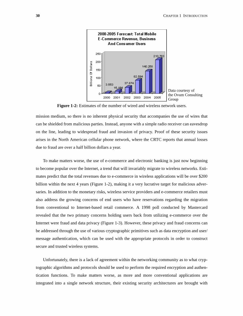
to become popular over the Internet, a trend that will invariably migrate to wireless networks. Esti-
mates predict that the total revenues due to e-commerce in wireless applications will be over $200
billion within the next 4 years (Figure 1-2), making it a very lucrative target for malicious adver-
saries. In addition to the monetary risks, wireless service providers and e-commerce retailers must
also address the growing concerns of end users who have reservations regarding the migration
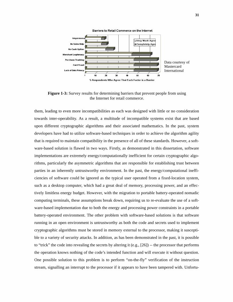
from conventional to Internet-based retail commerce. A 1998 poll conducted by Mastercard
revealed that the two primary concerns holding users back from utilizing e-commerce over the
Internet were fraud and data privacy (Figure 1-3). However, these privacy and fraud concerns can
be addressed through the use of various cryptographic primitives such as data encryption and user/
message authentication, which can be used with the appropriate protocols in order to construct
secure and trusted wireless systems.
Unfortunately, there is a lack of agreement within the networking community as to what cryp-
tographic algorithms and protocols should be used to perform the required encryption and authen-
tication functions. To make matters worse, as more and more conventional applications are
integrated into a single network structure, their existing security architectures are brought with
Figure 1-2: Estimates of the number of wired and wireless network users.
Data courtesy of the Ovum ConsultingGroup
31
them, leading to even more incompatibilities as each was designed with little or no consideration
towards inter-operability. As a result, a multitude of incompatible systems exist that are based
upon different cryptographic algorithms and their associated mathematics. In the past, system
developers have had to utilize software-based techniques in order to achieve the algorithm agility
that is required to maintain compatibility in the presence of all of these standards. However, a soft-
ware-based solution is flawed in two ways. Firstly, as demonstrated in this dissertation, software
implementations are extremely energy/computationally inefficient for certain cryptographic algo-
rithms, particularly the asymmetric algorithms that are responsible for establishing trust between
parties in an inherently untrustworthy environment. In the past, the energy/computational ineffi-
ciencies of software could be ignored as the typical user operated from a fixed-location system,
such as a desktop computer, which had a great deal of memory, processing power, and an effec-
tively limitless energy budget. However, with the migration to portable battery-operated nomadic
computing terminals, these assumptions break down, requiring us to re-evaluate the use of a soft-
ware-based implementation due to both the energy and processing power constraints in a portable
battery-operated environment. The other problem with software-based solutions is that software
running in an open environment is untrustworthy as both the code and secrets used to implement
cryptographic algorithms must be stored in memory external to the processor, making it suscepti-
ble to a variety of security attacks. In addition, as has been demonstrated in the past, it is possible
to “trick” the code into revealing the secrets by altering it (e.g., [26]) -- the processor that performs
the operation knows nothing of the code’s intended function and will execute it without question.
One possible solution to this problem is to perform “on-the-fly” verification of the instruction
stream, signalling an interrupt to the processor if it appears to have been tampered with. Unfortu-
Figure 1-3: Survey results for determining barriers that prevent people from usingthe Internet for retail commerce.
Data courtesy of MastercardInternational

32 CHAPTER 1 INTRODUCTION
nately, besides requiring a great deal of overhead to perform the verification, this too can be cir-
cumvented as the verifier is also external to the processor and hence susceptible to tampering. It is
possible to keep the secrets from being exposed by storing them in unflushable cache entries.
However, this is volatile memory that can be purged/cleared leading to possibly catastrophic con-
sequences from a security perspective (what do you do when your identification is erased?!).
A much better approach, and some would argue the only truly trustworthy approach, is to uti-
lize tamper-resistant hardware for performing cryptographic operations. With hardware the afore-
mentioned attacks become much more difficult (but not impossible [8]) as the secrets can be
contained within the processor using nonvolatile memory that is externally inaccessible. In addi-
tion, the “code” (i.e., the sequence of operations required to perform various cryptographic algo-
rithms) can be programmed into the hardware to ensure that nothing short of physical alteration of
the underlying hardware can cause incorrect operation. Dedicated hardware implementations can
be made very energy-efficient, thereby making them very attractive for energy-constrained appli-
cations such as the aforementioned portable terminals. The use of a dedicated cryptographic hard-
ware coprocessor also offloads the heavy computational demands of cryptographic algorithms
from the embedded general purpose processor, freeing it to perform other tasks to which it is better
suited.
Unfortunately, the single-purpose nature of existing cryptographic hardware means that multi-
ple hardware implementations are required to achieve algorithm-agility; otherwise the user will be
restricted to communicating securely only with systems using compatible algorithms. This access
restriction goes against the main advantage of wireless networks: the portability and convenience
of having access to the global web without having to be tied to a single access point and service
provider. Hence, it is advantageous, and one of the goals of this dissertation, to develop a hardware
based solution that is capable of providing algorithm-agility in an efficient manner so that it can be
used in the energy-constrained environments inherent in portable applications.
In addition to the desire for algorithm-agility, another goal of this dissertation is to provide a
general-purpose means of improving the energy efficiency of wireless systems. We accomplish
this by exploiting the fact that wireless systems exhibit time-varying quality1 requirements which
1. From the perspective of this dissertation, “quality” refers to both the level of security used for encrypting the wireless data stream, and the rate or throughput at which the encryption is per-formed (e.g., the highest quality corresponds to using strong encryption at high rates).
1.1 INTRODUCTION TO CRYPTOGRAPHY 33
allow us to dynamically adjust the system’s operating parameters such as the clock rate and supply
voltage in order to minimize the average energy consumption. We call this technique energy scal-
able computing and demonstrate its usefulness in an energy-efficient data encryption application.
1.1 Introduction to CryptographyCryptography is the science of encoding messages in such a way that unauthorized parties cannot
decipher the encoded information in a reasonable amount of time. In the past, the field of cryptog-
raphy was primarily the regime of the military, who used it for providing secure communication
channels in hostile environments. Most of the resulting encoding techniques were based on ad-hoc
methods that had no quantitative measure of security in either a practical or theoretical sense. In
the last 30 years though all of this has changed and cryptography has become more of a public sci-
ence due to its increased use in digital communications to provide security. Today, many important
results are being developed in the public domain, and formal methods have been developed and
refined for both the construction and analysis of cryptographic algorithms.
Unfortunately, cryptography has often been considered a black art, and the required mathemat-
ical foundations upon which it is built tend to dissuade most people from learning more about the
field. However, as digital communication channels continue to be trusted with more and more
valuable information such as financial transactions and electronic commerce, the science of cryp-
tography is beginning to become more mainstream due to the increasing awareness of security
issues. As a result, several excellent and easily accessible references for modern cryptography
have been developed and are currently available to the reader (e.g., [116] and [84]). This section
attempts to provide a brief introduction to the field, and highlight the main ideas in order to moti-
vate the work presented in this dissertation.
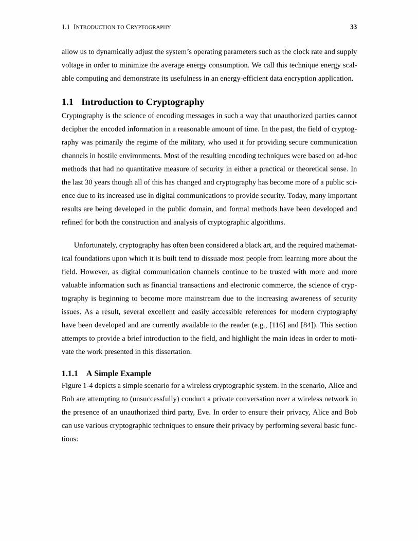
1.1.1 A Simple ExampleFigure 1-4 depicts a simple scenario for a wireless cryptographic system. In the scenario, Alice and
Bob are attempting to (unsuccessfully) conduct a private conversation over a wireless network in
the presence of an unauthorized third party, Eve. In order to ensure their privacy, Alice and Bob
can use various cryptographic techniques to ensure their privacy by performing several basic func-
tions:

34 CHAPTER 1 INTRODUCTION
• User Authentication: Alice and Bob must first verify to the others’ satisfaction thatthey are indeed who they say they are, and not just Eve impersonating either party.
• Key Agreement: Once Alice and Bob have verified their identities then they must beable to agree on some form of secret information that is known only to them and notEve. This secret information can then be used to construct a common secret key.
• Data Encryption/Decryption: With a shared secret key, Alice and Bob can then utilizedata encryption algorithms to encode their communication in such a way that Eve can-not decipher the message, even though she has full access to the encoded messages.
• Data Integrity Check and Signature: Ideally, Alice and Bob would like to be able toguarantee that the encoded messages they receive are the same as those sent, and thatthey were in fact sent by the other party and not Eve.
Cryptography enables techniques that can perform the above functions, utilizing two types of
algorithms (asymmetric and symmetric) which have distinctly different properties. Asymmetric
cryptographic algorithms get their name from the fact that they do not require any secret informa-
tion to be shared between Alice and Bob. Asymmetric algorithms rely on the existence of mathe-
matical functions that have the property that they can be computed efficiently (i.e., in polynomial
time), but are computationally infeasible to invert without knowing some secret piece of informa-
tion. The formal name for a function displaying these properties is a trapdoor one-way function;
one-way due to the asymmetry in computational complexity between the forward and inverse
paths, and trapdoor due to the existence of a secret piece of information that allows for efficient
inversion2. The asymmetry is exploited to form cryptographic algorithms which utilize two keys:
the public key, which is used to compute the forward function to encode the data, and the private
key (i.e., trapdoor) which enables the function to be inverted, thereby recovering the data that has
2. It is interesting to note that the existence of trapdoor one-way functions has yet to be proven. As it stands there are several functions such as integer factorization and discrete logarithms which are used in practical public key cryptography and appear to be good approximations.
Figure 1-4: Alice and Bob trying to conduct a private conversation over wirelesschannels and failing miserably as Eve listens in.
Alice Bob
Eve
The code is710125.
The code is710125.
The code is710125.

1.1 INTRODUCTION TO CRYPTOGRAPHY 35
been encoded. Asymmetric algorithms are commonly referred to as public key algorithms.
The separation of the key into a public and private component enables Alice and Bob to per-
form both user and data authentication by reversing encoding and decoding procedures: instead of
applying the public key to encode data and then the private key to decode, authentication primi-
tives use the private key to encode and public key to decode. Since the two operations commute,
the result is the same regardless of the order of application of the keys. Given that the private key is
known only by the user who generated it (e.g., Alice or Bob), Eve cannot impersonate either party
without guessing the correct key which is assumed to be computationally infeasible. Thus Alice
and Bob can authenticate their identities by agreeing on a message (e.g., “Hi, my name is Alice/
Bob”), encoding it with their private key, and then sending the encoded message along with the
public key to the other party, which can then decode using the public key to verify that the
expected message was received. Similarly, message authentication can be performed by having the
transmitter of the message encode a digital representation of the message using their private key to
form a digital signature of the message. The signature is then appended to the encoded message
and transmitted to the receiver. The receiver decodes the message, extracts the expected digital
representation from the message and then decodes the signature to ensure that it matches the
expected value. Any corruption of the transmitted message will result in the two values not match-
ing, thereby ensuring data authentication. In addition, since only the intended transmitter knows
the secret key value used to encode the signature, a successful decoding also validates the owner-
ship of the message.
Asymmetric techniques enable Alice and Bob to also generate a shared secret in the presence
of Eve by having each encode a randomly generated message using the others’ public key, and
then exchanging the two messages. Alice and Bob can then decode the others’ random message
and combine it in some pre-determined way with their own random message to generate a shared
secret key. Eve will only see the two encoded messages which, assuming the intractability of
inverting the public key encoding, doesn’t allow her to derive the same shared secret value. Hence,
Alice and Bob have performed key agreement as well.
Unfortunately, asymmetric algorithms derive their security from the hardness of the number
theoretic problem upon which they are built. This in turn limits the degree of optimizations that
can be applied to improve performance of the associated functions required to implement the
asymmetric algorithms. Hence, asymmetric algorithms tend to be very computationally inefficient,
36 CHAPTER 1 INTRODUCTION
and thus not a good choice for encrypting large amounts of data. Symmetric algorithms on the
other hand derive their security from a secret piece of information that is shared by the encoder
and decoder, commonly referred to as the secret key, which is why symmetric algorithms are typi-
cally referred to as secret key cryptography. The primary benefit of using secret key cryptography
is that the shared secret can be exploited to create algorithms that operate very efficiently in terms
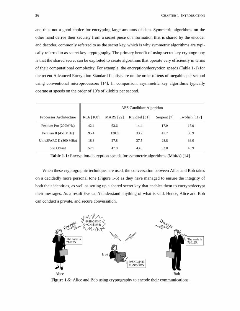
of their computational complexity. For example, the encryption/decryption speeds (Table 1-1) for
the recent Advanced Encryption Standard finalists are on the order of tens of megabits per second
using conventional microprocessors [14]. In comparison, asymmetric key algorithms typically
operate at speeds on the order of 10’s of kilobits per second.
When these cryptographic techniques are used, the conversation between Alice and Bob takes
on a decidedly more personal tone (Figure 1-5) as they have managed to ensure the integrity of
both their identities, as well as setting up a shared secret key that enables them to encrypt/decrypt
their messages. As a result Eve can’t understand anything of what is said. Hence, Alice and Bob
can conduct a private, and secure conversation.
AES Candidate Algorithm
Processor Architecture RC6 [108] MARS [22] Rijndael [31] Serpent [7] Twofish [117]
Pentium Pro (200MHz) 42.4 63.6 14.4 17.0 15.0
Pentium II (450 MHz) 95.4 138.8 33.2 47.7 33.9
UltraSPARC II (300 MHz) 18.3 27.8 37.5 28.8 36.0
SGI Octane 57.9 47.8 43.8 32.0 43.9
Table 1-1: Encryption/decryption speeds for symmetric algorithms (Mbit/s) [14]
Figure 1-5: Alice and Bob using cryptography to encode their communications.
Alice Bob
Eve
The code is710125.
8#$KC@H0+GN!$!##&
The code is710125.
8#$KC@H0+GN!$!##&
Encrypt Decrypt
1.1 INTRODUCTION TO CRYPTOGRAPHY 37
1.1.2 Secret Key Algorithm TypesThe family of secret key algorithms can be divided into two separate classes of algorithms known
as block and stream ciphers. As the name implies, block ciphers are symmetric key algorithms that
operate on blocks of data, n bits at a time, to generate a m-bit output that forms the encrypted mes-
sage. Obviously so that there will be an invertible mapping that can be decrypted, and typi-
cally m = n to avoid any data expansion. As a result, a block cipher can be thought of as a
memoryless n-bit permutation of the inputs under the influence of the secret key.
Stream ciphers on the other hand contain internal state that makes their output a time-depen-
dent function, thereby avoiding the replay weakness that haunts block ciphers. In addition, a
stream cipher operates on a data stream, typically a single bit wide, rather than a block of data. The
simplest model for a stream cipher is as a pseudo-random bit stream generator whose internal state
is a function of the secret key, and whose output can then be combined, typically via XOR, with
the data stream to form the encrypted data stream.
1.1.3 Public Key Algorithm Types
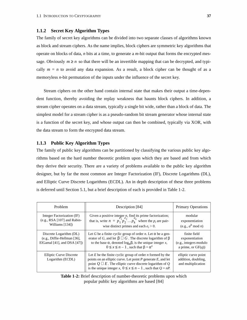
The family of public key algorithms can be partitioned by classifying the various public key algo-
rithms based on the hard number theoretic problem upon which they are based and from which
they derive their security. There are a variety of problems available to the public key algorithm
designer, but by far the most common are Integer Factorization (IF), Discrete Logarithms (DL),
and Elliptic Curve Discrete Logarithms (ECDL). An in depth description of these three problems
is deferred until Section 5.1, but a brief description of each is provided in Table 1-2.
Problem Description [84] Primary Operations
Integer Factorization (IF)(e.g., RSA [107] and Rabin-
Williams [134])
Given a positive integer n, find its prime factorization;
that is, write where the pi are pair-
wise distinct primes and each ei > 0.
modular
exponentiation
(e.g., ab mod n)
Discrete Logarithm (DL)(e.g., Diffie-Hellman [36],
ElGamal [41], and DSA [47])
Let G be a finite cyclic group of order n. Let α be a gen-erator of G, and let . The discrete logarithm of β
to the base α, denoted logαβ, is the unique integer x, , such that β = αx
finite fieldexponentiation
(e.g., integers modulo a prime, or GF(q))
Elliptic Curve DiscreteLogarithm (ECDL)
Let E be the finite cyclic group of order n formed by the points on an elliptic curve. Let point P generate E, and let point . The elliptic curve discrete logarithm of Q is the unique integer x, , such that Q = nP.
elliptic curve point addition, doubling, and multiplication
Table 1-2: Brief description of number-theoretic problems upon whichpopular public key algorithms are based [84]
m n≥
n p1
e1p2
e2…pk
ek=
β G∈
0 x n 1–≤ ≤
Q E∈0 x n 1–≤ ≤

38 CHAPTER 1 INTRODUCTION
1.1.4 Security Estimates for Asymmetric Cryptographic AlgorithmsThe security of asymmetric algorithms is expressed in terms of the computational complexity of
inverting the hard number-theoretic problem upon which they are based. As a result, security is
expressed in terms of asymptotic running times and big-oh notation (i.e., O(·)), which is a relative,
rather than absolute measure of security. What this means is that given the actual time required to
solve an m-bit instance of a problem which is assumed to have complexity O(f(m)), one can esti-
mate the amount of time required to solve a n-bit instance of the same problem using the relation:
(1-1)
Note that this is just an estimate, and as such it can be quite inaccurate. However, it is the most
widely accepted means of quantifying the security of asymmetric algorithms.
1.2 Previous WorkThe work described by this dissertation spans a wide array of research areas, ranging from hard-
ware-related fields such as low power circuit/system design and reconfigurable computing archi-
tectures, to the algorithms, mathematics, and implementation issues associated with various public
key cryptography schemes. As such there is a great deal of previous work that has been done in
regards to these areas and we attempt to provide a brief overview of each in order to put the work
described within this dissertation into context.
1.2.1 Low Power and Energy Efficient CMOS Design
The limited power budgets and energy reserves of portable, battery-operated computing devices
has made low power and energy efficient digital design methodologies an essential part of CMOS
VLSI design [24]. These methodologies attempt to reduce the power/energy consumption of inte-
grated circuits by minimizing the various components of the total power/energy consumption:
(1-2)
where α is the activity factor of the circuit being switched, C is the total switched capacitance, f is
the frequency at which the circuit is switched, and {Istatic, Ileakage, Ishort-circuit} are aggregate terms
corresponding to the sum of each currents’ components. In static digital CMOS design styles, such
as those used in this dissertation, the dominant term is the switching component (i.e., Ptotal ~
αCVDD2f). Hence, low power and energy efficient design methodologies attempt to minimize this
term through a variety of techniques and optimizations at all levels of the design hierarchy includ-
ing algorithm definition, architecture definition, and circuit design. A good comprehensive over-
T n( ) T m( ) O f n( )( )O f m( )( )--------------------⋅≈
Ptotal Pswitching Pstatic Pleakage Pshort circuit–+ + +
αCVDD2f IstaticVDD IleakageVDD Ishort circuit– VDD+ + +
=
=

1.2 PREVIOUS WORK 39
view of the subject is presented in [25].
1.2.2 Energy Efficient Reconfigurable Architectures
In the past research with regards to reconfigurable systems has largely ignored the issue of energy
efficiency, focusing only on the flexibility of the architecture in order to maximize its utility. In
commercial applications power/energy consumption is only a concern in respect to the thermal
effects that it introduces which are beginning to cause system failures. As a result, commercial
vendors have started to address power in a limited fashion through the use of low power (i.e., low
operating voltages of 1.8 or 2.5V) revisions of existing products (e.g., [9] and [136]). However, the
power/energy consumption of these devices is still significantly higher than what is required in the
energy-constrained environments discussed within this dissertation.
Academically, the issue of energy-efficient reconfigurable architectures is being addressed pri-
marily by Rabaey’s group at UC Berkeley with their Ultra Low-Power Reconfigurable Computing
project (i.e., Pleiades [102]). Rabaey’s group is attempting to develop energy-efficient reconfig-
urable architectures by quantifying the energy consumption within conventional programmable
architectures [75], and then developing both architectural and circuit-based techniques [50] to
minimize the energy consumption. The initial results appear to be quite promising, and they have
extended their work to the development of embedded reconfigurable logic cells in more conven-
tional signal-processing architectures in order to increase the utility of the overall system design
[141]. However, the limited size of their solutions precludes their use from public key cryptogra-
phy algorithms and thus work remains to be done regarding the design and implementation of
energy efficient reconfigurable cryptographic hardware.
1.2.3 Public Key Cryptographic Software
Many existing software implementations of public-cryptography can be found both in the com-
mercial and academic domains. Numerous companies such as RSA Security [111] and Certicom
[23] provide complete software implementations that can be purchased for use in commercial
applications. In addition, both shareware and freeware solutions exist as well such as PGP [142]
and Dai’s Crypto++ [32] packages. A comprehensive list of available shareware and freeware
implementations of RSA and Diffie-Hellman based public key cryptography can be found at
http://www.homeport.org/~adam/crypto/. The site also provides hypertext links to
the various packages for easy downloading.
In the late 70’s and early 80’s there was considerable work done on developing fast techniques
40 CHAPTER 1 INTRODUCTION
and algorithms for implementing common algorithms based on modular exponentiation such RSA
[107] and Diffie-Hellman [36] in software. A very good summary of these methods as they pertain
to implementing RSA, and by extension Diffie-Hellman, is given by Koc in [68]. Several of these
techniques such as Montgomery’s method [87], the Karatsuba-Ofman algorithm [63], and
Comba’s Method [29] are used to improve the performance of the software implementation
described within this dissertation. In addition, Gordon [51] provides a comprehensive overview of
optimizations for the modular exponentiation operation that dominates the performance of these
cryptosystems.
The recent popularity of Elliptic Curve Cryptography, and its extensive use of Galois Field
theory has led to several recently published works regarding fast software implementations of both
the underlying Galois Field arithmetic and the elliptic curve algorithms (e.g., [12], [15], [34], [35],
[52], [54] and [118]). These operations utilize arithmetic over both GF(2n) and GF(pn), where p is
a prime of special form (e.g., Mersenne primes) that allows for very fast modular multiplication to
be performed as demonstrated by the work on Optimal Extension Fields by Bailey and Paar [12].
Arithmetic over GF(2n) can be performed using either conventional extension fields of order n
(e.g., [118]), or composite fields of the form GF((2k)l) where k·l = n (e.g., [15], [34], and [54]).
Composite fields provide certain computational advantages to conventional extension fields in that
various table-lookup methods can be utilized to speed up the computation. However, the additional
structure introduced by the composition of fields may ultimately prove to allow for faster attacks
in elliptic curve applications, as was discovered for conventional Diffie-Hellman type applications
[3]. Many of the techniques for RSA and Diffie-Hellman type algorithms have direct analogs in
elliptic curve cryptography (e.g., Karatsuba-Ofman algorithm applied to composite field arith-
metic [52]), and hence much of that work can (and has) be applied here as well.
In all of the above implementations, all quantitative analysis focuses entirely on the speed at
which the arithmetic can be performed. There is no mention of the energy efficiency of these oper-
ations, and how they relate to their hardware counterparts. As such, there is still work that must be
done to characterize this aspect of the implementation in order to determine the suitability of soft-
ware-based solutions in energy-constrained environments.
1.2.4 Public Key Cryptographic Hardware
From a hardware perspective, the RSA public key cryptography algorithm is by far the most
widely studied, due in large part to the algorithm’s widespread industrial acceptance. All of the
1.2 PREVIOUS WORK 41
reported work for RSA-type modular exponentiations hardware feature similar architectures using
some form of repeated modular square-and-multiply exponentiation algorithm. These architec-
tures feature either a single modular multiplier to perform the required operations serially, or two
modular multipliers to compute the modular squaring and multiply operations concurrently using
two explicit modular multiplication units, or a single pipelined unit with the operations inter-
leaved. The modular multiplication operation is performed using either conventional concurrent
multiply-and-divide type algorithms ([1], [59], [95], [113], [119], [121], and [128]), or Montgom-
ery’s method ([40], [57], [77], [94], [110], [131], [138], and [139]). An alternative approach uti-
lizes systolic arrays for modular multiplication/exponentiation ([28], [53], [61], [114], [127], and
[130]), though they are not typically used due to their large area and latency requirements. High
performance is typically achieved by using a redundant internal representation to eliminate time-
consuming carry propagation chains within the multiplier, although one novel implementation
[113] utilizes a very fast binary adder architecture (which is also used within this dissertation) that
enables a non-redundant internal format.
Koc provides a comprehensive, though somewhat dated overview of various hardware tech-
niques and architectures for implementing fast modular exponentiation in hardware in [69]. In
addition, Beth and Gollmann also provide an overview of hardware implementation alternatives
for modular exponentiation functions in [17].
Hardware implementations for Discrete Logarithm based public key cryptography overlap
substantially with those of RSA-based implementations due to the fact that they both may be
implemented using modular exponentiation over integer fields. In DL-based systems the modulus
must be prime, while RSA-based systems utilize a composite modulus. However, in both cases the
modulus is odd and the same hardware can be used. Hence, all of the aforementioned references
apply for DL-based systems as well.
A small number of systems for DL-based systems over GF(pm) have also been reported for p =
2, though for the most part their small field sizes (GF(2127) [140] and GF(2593) [5]) preclude their
use from modern applications where security requirements dictate the use of extensions on the
order of 1000. Mastrovito Ph.D. Thesis [80] provides a very comprehensive overview of efficient
hardware VLSI architectures for performing arithmetic over GF(2n) using bit-serial implementa-
tions that are applicable to the large field sizes required by cryptographic applications. Beth and
Gollmann’s overview also discusses various implementations of GF(2n) arithmetic using very

42 CHAPTER 1 INTRODUCTION
area-efficient bitsliced implementations that map well to cryptographic applications. In addition,
Geiselmann and Gollmann [49] describe efficient architectures for implementing GF(2n) exponen-
tiation in both Normal and Standard bases for cryptographic applications.
The small field sizes required for implementing elliptic curve cryptography have led to effi-
cient software-based implementations, and as a result there has been little reported work regarding
hardware implementations of elliptic curve cryptography systems. The main work that has been
reported was done by Agnew [6] in which a GF(2155) ALU is used to perform elliptic curve oper-
ations. Their work utilized the existence of an optimal normal basis (ONB) over GF(2155) in order
to perform multiplication in a very efficient manner using a modified Massey-Omura ONB multi-
plier [91]. The work of Agnew is essentially duplicated in the work of Sutikno in [123] (and [124]
where they duplicate their own work using FPGA’s). Paar and Soria-Rodriguez describe an effi-
cient hardware architecture for GF(2n) in [96] that utilizes the composite decomposition of the
field GF(2n) = GF((2k)l) to develop what is essentially a linear-feedback shift register over GF(2l)
with all component-wise multiplications and additions are performed over GF(2k). The resulting
implementation is general in that the value of l can be changed, leading to a limited degree of flex-
ibility.
However, in all previous work the resulting hardware implementations are specific to a single
type of arithmetic/public key algorithm; no previous example of a dedicated hardware-based solu-
tion that is capable of performing conventional, modular integer, GF(2n), and elliptic curve arith-
metic could be found.
1.3 Thesis Overview and ContributionsThis dissertation begins with an overview of the required number theory in Chapter 2 which serves
as the foundation upon which much of the subsequent chapters are built. The intention is to pro-
vide enough detail to make the work that follows decipherable, without getting bogged down in
the mathematics. Hence, only material that is directly relevant to the subsequent discussions is
described.
The first contribution of this dissertation is presented in Chapter 3, with the development and
implementation of optimized software-based libraries of different families of public key cryptog-
raphy algorithms. Both the performance and energy-efficiency of the resulting implementations
are quantified and compared. In addition, a modified multiplier architecture is proposed that
1.3 THESIS OVERVIEW AND CONTRIBUTIONS 43
requires only a small modification to the processor’s existing integer multiplier which yields an
order of magnitude better performance for GF(2n)-based cryptographic algorithms implemented in
software.
The first thesis of this dissertation is presented in Chapter 4:
Energy Scalability: The time-varying data rates and quality requirements that areinherent in wireless communications can be exploited to significantly reduce theenergy consumption of the system by exploiting energy scalable architectures todynamically trade-off the energy being dissipated as a function of the desired levelof quality and throughput.
The chapter begins by introducing the notion of energy scalable computing, motivates its use, and
describes a design example involving the design and implementation of an energy scalable encryp-
tion processor that features a high-efficiency, embedded programmable DC/DC converter. The
chapter concludes with a presentation of experimental results that validate the thesis of energy
scalability, and a comparison to conventional software-based solutions.
Chapter 5 addresses the second thesis of this dissertation:
Domain Specific Reconfigurability: For the application of public key cryptogra-phy, one can define a domain of required functions and utilize limited reconfig-urability to develop a domain specific reconfigurable hardware implementationthat combines the algorithm-agility of a software-based solution and the perfor-mance and energy efficiency of a hardware-based solution, without the high over-head costs typically associated with generic programmable logicimplementations.
The chapter starts with a discussion of the need for algorithm agility in public key cryptography
and a description of the recent IEEE P1363 Standard for Public Key Cryptography. The problems
with general purpose programmable logic solutions are then described, and the notion of domain
specific reconfigurability is introduced. The remainder of the chapter describes the design and
implementation of a reconfigurable processor for public key cryptography that provides all of the
required algorithm-agility for implementing the primitives of P1363. The chapter concludes with
the presentation of experimental results and a comparison to both conventional programmable
logic-based solutions, and the software-based solutions developed in Chapter 3. These results vali-
date the thesis of domain specific reconfigurability as it pertains to public key cryptography.
The dissertation concludes in Chapter 6 with a discussion of the results of this work. Future
research activities are also proposed for furthering both the work described within this dissertation,
and the field of hardware implementations of cryptography in constrained environments.

44 CHAPTER 1 INTRODUCTION
454545
Chapter 2
A Primer in Number Theory and Elliptic CurvesThe work described in this dissertation describes various aspects of implementing cryptographic
algorithms which requires some form of mathematical overview in order to properly define terms
and concepts that will be used extensively in subsequent chapters. However, it is easy to become
lost in the math, which would render the dissertation unusable. Hence, care has been taken to only
discuss and define those topics that are absolutely necessary, and the reader is referred to any of the
multitude of excellent references on number theory (e.g., [67], [78], [79], and [11]) for additional
material that is considered beyond the scope of this dissertation.
2.1 Groups, Rings, and FieldsThe primary mathematical constructs used in public key cryptography are those of a finite group,
ring, and field. Each of these constructs consists of a non-empty set of elements together with one
or more functions which operate on elements of the set to generate other elements of the set. The
most general, and hence least constrained, of these structures is that of an abelian group, which is
formally defined below.
Definition 1: An abelian group, G, is a non-empty set of elements together with a binary operator• which exhibit the following properties:
1. for all (i.e., G is closed under the operation •)2. for all (i.e., • obeys the associative law)3. There exists an identity element for all such that 4. For all , there exists an inverse element such that 5. for all (i.e., • is commutative)
An example of an abelian group would be that of the integers under the addition operation,
a b• G∈ a b G∈,a b c•( )• a b•( ) c•= a b c, G∈,
e G∈ a G∈ a e• e a• a= =a G∈ a
1–G∈ a a
1–• e=a b• b a•= a b G∈,

46 CHAPTER 2 A PRIMER IN NUMBER THEORY AND ELLIPTIC CURVES
with the identity element e = 0, and inverse a-1 = -a. In cryptography the groups used typically
have a finite number of elements, the number of which is referred to as the order of the group. A
finite group G is said to be cyclic if all elements of the group can be generated by repeated applica-
tions of the group operation “•” to an element which is denoted as a generator of the group
G. The order of an element a of a finite cyclic group G is the smallest positive integer b such that
(2-1)
and is denoted as ord(a) = b. Hence, the order of a generator of G will be the order of the group,
and the order of any element will always divide the group order. Thus ord(G) = c·ord(a) for
some positive integer c.
The finite abelian group serves as the basic structure upon which cryptographic systems can be
constructed. The definition of a group can be enhanced by adding an additional operator and prop-
erties, in which case it becomes a ring:
Definition 2: A ring, R, is a non-empty set of elements together with two binary operators, + and •(commonly denoted as “addition” and “multiplication” respectively), which exhibit the followingproperties:
1. R is an abelian group under the operation +.2. R is closed under the operation •.3. • obeys the associative law over R.4. For all , and (i.e., dis-
tributivity applies)
The most common, and in some sense most powerful, mathematical structure is that of the
field, which is essentially a ring with additional properties that guarantee the existence of an iden-
tity and inverse element under both addition and multiplication. In a more formal sense, a field
exhibits the following properties:
Definition 3: A field, F, is a non-empty set of elements together with two binary operators, + and •,which exhibit the following properties:
1. F is an abelian group under the operation +.2. The non-zero elements of F form an abelian group under the operation •.3. Distributivity over (+, •) applies.
Given a finite field with q elements, we commonly refer to it as a Galois Field, denoted as
GF(q), which can be shown to be unique and to exist for all q = pm, p prime [79]. Furthermore, it
can also be shown that the set of integers modulo a prime p (i.e., Zp) is a field [79].
a G∈
a a a…a a••• e=
a G∈
a b c, R∈, a b c+( )• a b• a c•+= b c+( ) a• b a c a•+•=
b applications of “•”
2.1 GROUPS, RINGS, AND FIELDS 47
The characteristic of a field GF(q) is defined to be the smallest positive integer k for which
, for all . In the case of GF(pm), p prime, the characteristic will be p.
2.1.1 Field Polynomials and Extension FieldsGiven a field GF(q), it is possible to construct a polynomial over GF(q) of the form:
(2-2)
where . The degree of f(x) is the largest value of i for which fi is non-zero, and the
polynomial is said to be monic if it’s degree is maximal (e.g., m in EQ 2-2).
Addition, multiplication, and division of polynomials over GF(q) is performed using conven-
tional polynomial addition (e.g., component-wise), multiplication (e.g., convolution), and division
(e.g., long-division) techniques, with the component addition/multiplication being performed over
GF(q). The resulting set of polynomials will form a polynomial ring denoted F[x]GF(q).
Definition 4: A polynomial is said to be irreducible if it is only divisible byeither a·f(x), or a·1 for some .
Definition 5: A monic irreducible polynomial f(x) of degree m over GF(q) is said to be primitive ifthe smallest positive integer k for which f(x) divides xk - 1 evenly without remainder is qm - 1.
Given a polynomial ring F[x] and an irreducible polynomial f(x) of degree m over GF(q), the
residue class formed by the polynomials modulo-f(x) of F[x] (i.e., F[x]/f(x))3 forms an extension
field of GF(q), denoted GF(qm). The field GF(qm) has order qm, and its elements can be interpreted
as the set of polynomials of degree k < m over GF(q). For example, the irreducible polynomial
over GF(2) generates the residue class {0, 1, x, x + 1}, which constitutes the
extension field GF(22).
2.1.2 Composite Fields
A similar construction to an extension field is a composite field which is formed by composing an
extension of an extension field (e.g., GF((pk)l)). The first extension of GF(p) to GF(pk) is per-
formed using the irreducible polynomial N(x) of degree k over GF(p), and the second extension
from GF(pk) to GF((pk)l) is performed using the irreducible polynomial M(x) of degree l over
GF(pk).
3. Modular reduction by the irreducible polynomial f(x) is performed using standard polynomial long-division techniques with all component-wise operations performed over GF(q).
k a⋅ 0= a GF q( )∈
f x( ) fmxm … f1x f0+ + + fix
i
m
∑= =
fi GF q( )∈
f x( ) F x[ ] GF q( )∈a GF q( )∈
f x( ) x2
x 1+ +=

48 CHAPTER 2 A PRIMER IN NUMBER THEORY AND ELLIPTIC CURVES
The benefit of using composite fields is that, while being isomorphic to GF(pn) for n = k·l, the
complexity of their associated field operations can differ substantially from that of GF(pn) depend-
ing on the choices of k and l (e.g., [37], [96]). However, the additional structure that is imposed by
the composite nature of the field also allows for accelerated attacks on composite fields for crypto-
graphic systems built upon the Discrete Logarithm assumption [3], rendering them unusable in
these situations. However, the use of composite fields for constructing elliptic curves doesn’t seem
to introduce similar problems for the Elliptic Curve Discrete Logarithm problem. However, it’s
reasonable to assume that the additional structure of the composite field will likely detract from its
security, rather than enhance it. Hence, the decision was made for the course of this dissertation to
utilize only fields of the form GF(pm), p prime.
2.1.3 Basis RepresentationThe extension field GF(pm) can be interpreted as a vector space of dimension m, which introduces
an additional degree of freedom during implementation in terms of selecting the basis used to rep-
resent elements of the field. The two most common types of bases used in conventional hardware
and software implementations are the standard and normal bases. Other, less commonly used bases
such as the dual [16] and triangular bases [55] have advantages in certain implementations but are
considered outside the scope of this dissertation.
In a standard basis the elements of GF(pm) are represented as linear combinations of the basis
set {1, α, α2,. . ., αm-2, αm-1}, where α is a root of the irreducible polynomial used to construct the
field GF(pm) from GF(p). Hence, given an element , it can be expressed as
(2-3)
In a standard basis the basis vectors αi are represented by the polynomials xi, and thus any element
of GF(pm) can be expressed as a polynomial of degree < m. This interpretation of elements of
GF(pm) as polynomials is why the standard basis is also commonly referred to as a polynomial
basis.
A normal basis (NB) is formed by selecting an element , such that the m ele-
ments of the set
(2-4)
are linearly independent. The primary advantage of using a normal basis is that exponentiation by
a GF pm( )∈
a a0α0 a1α1 … am 2– αm 2– am 1– αm 1–+ + + +=
β GF pm( )∈
β βp βp2
… βpm 2–
βpm 1–
, , , , ,
2.2 ELLIPTIC CURVES 49
p is a linear operation requiring only a circular right shift of the coefficients. Hence, operations that
require repeated exponentiations by p, such as exponentiation and inversion, can be implemented
very efficiently. The cost of using a normal basis is that multiplication is much more complex
operation than in a standard basis, though for certain values m an optimal normal basis [89] can be
constructed to minimize the multiplication complexity.
2.2 Elliptic CurvesOne of the primary mathematical constructs used in contemporary public key cryptography is the
Elliptic Curve. Elliptic Curve Cryptography (ECC) was initially proposed by both Koblitz [65]
and Miller [85] in 1985, and has recently become very popular due to its apparent security advan-
tages over more conventional approaches (e.g., RSA [107] and Discrete Logarithm based
approaches). This section attempts to discuss the primary mathematical results in regards to Ellip-
tic Curves that are used in ECC systems.
Definition 6: Given a field F, an elliptic curve E, is defined to be those points (X,Y,Z), satisfying the general projective form of a homogeneous Weisterass Equation:
(2-5)
where . The resulting set of points, plus an additive identity defined as thepoint at infinity (O) which has the value (X,Y,Z) = (0,1,0), together with a point “addition” opera-tion form an additive group.
2.2.1 Affine vs. Projective Co-ordinates
An alternative representation for the curve E utilizes the change of variables y = (Y/Z), x = (X/Z), in
which case EQ 2-5 becomes:
(2-6)
Removing the common Z3 term yields the affine form of the Weisterass Equation:
(2-7)
Unlike its projective counterpart, in affine co-ordinates the point at infinity (O) doesn’t have a
corresponding co-ordinate value. Instead the point at infinity is commonly mapped to the point
(X,Y) = (0,0), an invalid curve point for , which simplifies the implementation of point
validity checking and eliminates the need for a special symbol designation.
The decision regarding whether to use projective or affine co-ordinates is based primarily on
implementation aspects regarding the availability of memory for storing temporary values and the
relative performance of the field inversion and multiplication algorithms used to implement the
X Y Z, ,{ } F∈
E : Y2Z a1XYZ a3YZ
2+ + X
3a2X
2Z a4XZ
2a6Z
3+ + +=
a1 a2 a3 a4 a6, , , ,{ } F∈
E : y2Z
3a1xyZ
3a3yZ
3+ + x
3Z
3a2x
2Z
3a4xZ
3a6Z
3+ + +=
E : y2
a1xy a3y+ + x3
a2x2
a4x a6+ + +=
a6 0≠

50 CHAPTER 2 A PRIMER IN NUMBER THEORY AND ELLIPTIC CURVES
group operations of point addition and doubling. In affine co-ordinates, on a curve constructed
over the field GF(2n), point addition and doubling can be implemented in one inversion, two mul-
tiplications, and one squaring over GF(2n) using EQ 2-27 and EQ 2-28 respectively. A projective
implementation can perform the same operations using 15 multiplications and five squarings for a
point addition (EQ 2-8), and five multiplications and five squarings for a point doubling (EQ 2-9).
In terms of memory requirements the affine implementation requires two temporary variables for
both point addition and doubling, while a projective implementation requires either nine or four
temporary variables for point addition and doubling respectively.
(2-8)
(2-9)
The benefit of using projective co-ordinates is that the group operations do not require field
inversions which can be very slow operations if they are not implemented correctly. If Tinvert >
13·Tmult + 4·Tsquare then projective point addition is faster, and similarly, if Tinvert > 3·Tmult +
4·Tsquare then projective point doubling is faster. However, for the implementation of GF(2n) arith-
metic described within this dissertation, inversion can be implemented quite efficiently in both
hardware and software so there is no need to incur the high storage and computation overhead of
projective co-ordinates. Hence, only affine co-ordinate representations will be discussed for the
P1 P2+ X3 Y3 Z3, ,( )λ1 X1Z2
2
λ2 X2Z12
λ3 λ1 λ2
λ4
+
Y1Z23
λ5 Y2Z13
λ6 λ4 λ5
λ7
+
Z1λ3
λ8 λ6X2 λ7Y2
Z3
+
λ7Z2
λ9 λ6 Z3
X3
+
a2Z32 λ6λ9 λ3
3
Y3
+ +
λ9X3 λ8λ72+
=
=
=
=
=
=
=
=
=
=
=
=
=
2P1 X3 Y3 Z3, ,( )
Z3 X1Z12
X3 X1 a6Z12
+( )4
λ Z3 X12
Y1Z1
Y3
+ +
X14Z3 λX3+
=
=
=
=
=

2.2 ELLIPTIC CURVES 51
remainder of this dissertation.
2.2.2 Supersingular vs. Non-supersingular Elliptic Curves
Given a particular elliptic curve E, and its associated parameters {a0, a1, a2, a3, a4, a5, a6}, two
curve parameters denoted as the discriminant (∆) and j-variant (j(E)) can be derived. Depending on
characteristic of the base field over which the curve is defined (i.e., 2 or some prime > 3), the
resulting values of ∆ and j(E) categorize the curve as being either supersingular or non-supersingu-
lar. From a cryptographic standpoint, supersingular curves should be avoided as they allow for a
transformation that maps the ECDL problem upon which the security of ECC is built, to a conven-
tional DL problem (the MOV attack [82]) which is much less secure in terms of the asymptotic
time complexity required to break the system. Hence, the security of the system is compromised.
To ensure that a non-supersingular curve is chosen, one can use the following curve selection/
construction criteria:
• characteristic = 2: given the simplified affine Weisterass Equation y2 + a1xy = x3 +a2x2 + a6, ensure (typically a1 = 1 is chosen to simplify the arithmetic).
• characteristic > 3: given the simplified affine Weisterass Equation of y2 = x3 + ax + b,ensure that .
A discussion of both the discriminant and j-variant, as well as how to compute their values is
deemed beyond the scope of this dissertation, and the reader is referred to any of the excellent ref-
erences on Elliptic Curves such as [18], [66], and [81].
2.2.3 Point Addition and DoublingGiven the general affine form of an elliptic curve (EQ 2-7), one can define the group operation of
adding two points together. Given two distinct points, P1 = (x1,y1) and P2 = (x2,y2) lying on E,
their sum, assuming , is defined as that point P3 = P1 + P2 which is the reflection about the
x-axis of the point of intersection of the line containing P1 and P2, and the curve E (e.g., Figure 2-
1(a)). If the two points have the same x ordinate, then the resulting line containing the points will
be vertical, and have an ill-defined intersection point to the curve. In these cases the line is said to
intersect the curve at the point at infinity. Given a single point, P1 = (x1,y1), the sum of that point
with itself (i.e., the doubling of the point), can be defined as the point P3 = 2P1 which is the reflec-
tion about the x-axis of the point of intersection of the line tangent to E at point P1, and the curve E
(e.g., Figure 2-1(b)).
a1 0≠
4a3
27b2
0≠+
x1 x2≠
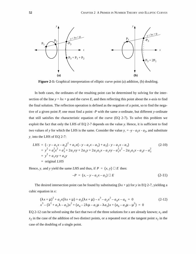
52 CHAPTER 2 A PRIMER IN NUMBER THEORY AND ELLIPTIC CURVES
In both cases, the ordinates of the resulting point can be determined by solving for the inter-
section of the line y = λx + µ and the curve E, and then reflecting this point about the x-axis to find
the final solution. The reflection operation is defined as the negation of a point, so to find the nega-
tive of a given point P, one must find a point -P with the same x-ordinate, but different y-ordinate
that still satisfies the characteristic equation of the curve (EQ 2-7). To solve this problem we
exploit the fact that only the LHS of EQ 2-7 depends on the value y. Hence, it is sufficient to find
two values of y for which the LHS is the same. Consider the value y- = -y - a1x - a3, and substitute
y- into the LHS of EQ 2-7:
(2-10)
Hence, y- and y yield the same LHS and thus, if then:
(2-11)
The desired intersection point can be found by substituting (λx + µ) for y in EQ 2-7, yielding a
cubic equation in x:
(2-12)
EQ 2-12 can be solved using the fact that two of the three solutions for x are already known; x1 and
x2 in the case of the addition of two distinct points, or a repeated root at the tangent point x1 in the
case of the doubling of a single point.
P1
P2
P3 = P1 + P2
x
y
y = λx + µP1
P3 = 2P1
x
y
y = λx + µ
(a) (b)
-P3
-P3
Figure 2-1: Graphical interpretation of elliptic curve point (a) addition, (b) doubling.
LHS y– a1x– a3–( )2a1x y– a1x– a3–( ) a3 y– a1x– a3–( )+ +
y2
a12x
2a3
22a1xy 2a3y 2a1a3x a1xy– a1
2x
2– 2a1a3x– a3y– a3
2–+ + + + +
y2
a1xy a3y+ +
original LHS
=
=
=
=
P x y,( ) E∈=
P– x y– a1x– a3–,( ) E∈=
λx µ+( )2a1x λx µ+( ) a3 λx µ+( ) x
3– a2x
2– a4x– a6–+ + 0
x3 λ2
a1λ a2–+( )x2
– a4 2λµ– a1µ– λa3–( )x a6 a3µ– µ2–( )+ + 0
=
=
2.2 ELLIPTIC CURVES 53
Consider first the case when two distinct points are added together. Given that the points x1, x2,
and x3 all lie at intersection points, the solution to EQ 2-12 can be expressed in factored form:
(2-13)
Equating coefficients of the quadratic terms of EQ 2-12 and EQ 2-13 gives the value of x3 directly:
(2-14)
In the case of a point doubling, the root x1 will be repeated and the solution to EQ 2-12 can be
expressed in factored form as
(2-15)
which yields:
(2-16)
Note that EQ 2-16 is identical to EQ 2-14 with the substitution x2 = x1.
The y-ordinates can then be derived using the result of EQ 2-10, and the fact that along the line
of intersection y = λx + µ:
(2-17)
Given the above expressions for point addition/doubling, the only unknowns remaining are the
slope (λ) and intercept (µ) values of the intersection line. In the case of two distinct points P1 and
P2, the values of λ and µ can be derived from solving the simple system of two equations with two
unknowns to get:
(2-18)
(2-19)
If P1 = P2, then λ can be determined by implicitly differentiating EQ 2-7 to get:
(2-20)
x x1–( ) x x2–( ) x x3–( ) x3
x1 x2 x3+ +( )x2
– x1x2 x1x3 x2x3+ +( )x x1x2x3–+=
λ2a1λ a2–+ x1 x2 x3
x3⇒+ +
λ2a1λ a2– x1– x2–+
=
=
x x1–( )2x x3–( ) x
32x1 x3+( )x
2– x1
22x1x3+( )x x1
2x3–+=
x3 λ2a1λ a2– 2x1–+=
y3 y– a1x3– a3–λx3 µ+( )– a1x3– a3–λ a1+( )x3– a3– µ–
===
λy2 y1–
x2 x1–----------------=
µx2y1 x1y2–
x2 x1–---------------------------=
2ydydx------ a1y a1x
dydx------+ a3
dydx------+ + 3x
22a2x a4
λ dydx------=⇒
+ +
3x2
2a2x a4 a1y–+ +
2y a1x a3+ +----------------------------------------------------
=
=

54 CHAPTER 2 A PRIMER IN NUMBER THEORY AND ELLIPTIC CURVES
and µ can be determined using the relation µ = y - λx:
(2-21)
but , so:
(2-22)
The above equations can be further simplified by exploiting isomorphisms that exist depend-
ing on the characteristic of the field over which the Elliptic Curve is being implemented.
Curves in fields of characteristic p > 3: If p > 3, an isomorphism exists that enables EQ 2-6 to be
simplified to:
(2-23)
which is equivalent to setting a1 = a2 = a3 = 0, a4 = a, and a6 = b. These simplifications yield the
following expressions for point addition and doubling:
(2-24)
(2-25)
Curves in fields of characteristic p = 2: In fields of characteristic 2, an isomorphism exists that
simplifies EQ 2-6 to:
(2-26)
which is equivalent to setting a1 = 1 and a3 = a4 = 0. These simplifications, combined with the
modulo-2 reduction of coefficients and equivalency of addition and subtraction over GF(2n), yield
µ∴ y3x
22a2x a4+ +
2y a1x a3+ +--------------------------------------x–
2y2
2a1xy a3y 3x3
– 2a2x2
– a4x–+ +
2y a1x a3+ +---------------------------------------------------------------------------------------------
2 y2
a1xy a3y+ +( ) 3x3
– 2a2x2
– a4x– a3y–
2y a1x a3+ +-------------------------------------------------------------------------------------------------------------
=
=
=
y2
a1xy a3y+ + x3
a2x2
a4x a6+ + +=
µ2 x
3a2x
2a4x a6+ + +( ) 3x
3– 2a2x
2– a4x– a3y–
2y a1x a3+ +------------------------------------------------------------------------------------------------------------------------
x3
– a4x 2a6 a3y–+ +
2y a1x a3+ +------------------------------------------------------
=
=
E : y2
x3
ax b+ +=
1 P2+ x3 y3,( )x3 λ2
x1– x2
y3
–
x1 x3–( )λ y1
λ
–
y2 y1–( ) x2 x1–( )⁄
=
=
=
=
2P1 x3 y3,( )x3 λ2
2x1
y3
–
x1 x3–( )λ y1
λ
–
3x12
a+( ) 2y1⁄
=
=
=
=
E : y2
xy+ x3
a2x2
a6+ +=
2.2 ELLIPTIC CURVES 55
the following expressions for point addition and doubling:
(2-27)
(2-28)
2.2.4 Point Order
As discussed in Section 2.1, the cyclic nature of the additive group formed by the points on an
elliptic curve over GF(q) implies that repeated application of the group operation to a point on the
curve will eventually result in the generation of the original point again. Mathematically speaking
this means that for some integer n, and some point P on the elliptic curve E, the following relation
will hold:
(2-29)
where the value n is called the order of point P on E, and corresponds to the number of points in
the cyclic subgroup of E of which P is a member. For cryptographic applications, n should be a
large prime at least 130 bits long.
The existence of a subgroup of E with the desired properties can be guaranteed by exploiting
the fact that the order of any subgroup (which is defined by the order of a point that generates the
subgroup) will divide the order of the curve E, denoted #E. #E can be computed using Schoof’s
Algorithm [115] and then factored using conventional factoring algorithm (e.g., [76], [99]) to
determine if it has a subgroup with a sufficiently large prime factor. If not, or if the factoring oper-
ation does not complete within a reasonable amount of time, another curve E is chosen at random
and the process is repeated.
Assuming that a subgroup exists with sufficiently large enough prime order, one must still
choose a point P which generates the subgroup. Fortunately, this can be done quite easily by
selecting random points on the curve and testing if they have the correct order by using point mul-
tiplication to verify
(2-30)
P1 P2+ x3 y3,( )x3 λ2 λ x1 x2 a
y3
+ + + +
x2 x3+( )λ x3 y2
λ
+ +
y1 y2+( ) x1 x2+( )⁄
=
=
=
=
2P1 x3 y3,( )x3 λ2 λ a
y3
+ +
x1 x3+( )λ x3 y1
λ
+ +
x1 y1 x1⁄+
=
=
=
=
n 1+( )P P=
nP O=

56 CHAPTER 2 A PRIMER IN NUMBER THEORY AND ELLIPTIC CURVES
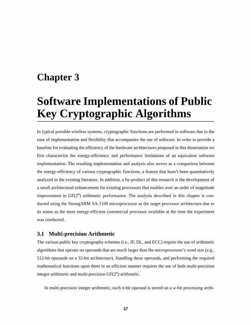
575757
Chapter 3
Software Implementations of Public Key Cryptographic AlgorithmsIn typical portable wireless systems, cryptographic functions are performed in software due to the
ease of implementation and flexibility that accompanies the use of software. In order to provide a
baseline for evaluating the efficiency of the hardware architectures proposed in this dissertation we
first characterize the energy-efficiency and performance limitations of an equivalent software
implementation. The resulting implementation and analysis also serves as a comparison between
the energy-efficiency of various cryptographic functions, a feature that hasn’t been quantitatively
analyzed in the existing literature. In addition, a by-product of this research is the development of
a small architectural enhancement for existing processors that enables over an order of magnitude
improvement in GF(2n) arithmetic performance. The analysis described in this chapter is con-
ducted using the StrongARM SA-1100 microprocessor as the target processor architecture due to
its status as the most energy-efficient commercial processor available at the time the experiment
was conducted.
3.1 Multi-precision ArithmeticThe various public key cryptography schemes (i.e., IF, DL, and ECC) require the use of arithmetic
algorithms that operate on operands that are much larger than the microprocessor’s word size (e.g.,
512-bit operands on a 32-bit architecture). Handling these operands, and performing the required
mathematical functions upon them in an efficient manner requires the use of both multi-precision
integer arithmetic and multi-precision GF(2n) arithmetic.
In multi-precision integer arithmetic, each n-bit operand is stored on a w-bit processing archi-
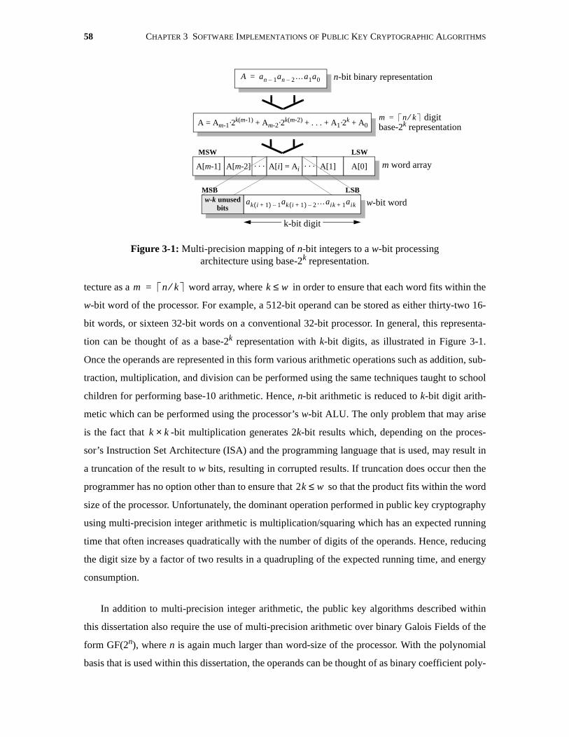
58 CHAPTER 3 SOFTWARE IMPLEMENTATIONS OF PUBLIC KEY CRYPTOGRAPHIC ALGORITHMS
tecture as a word array, where in order to ensure that each word fits within the
w-bit word of the processor. For example, a 512-bit operand can be stored as either thirty-two 16-
bit words, or sixteen 32-bit words on a conventional 32-bit processor. In general, this representa-
tion can be thought of as a base-2k representation with k-bit digits, as illustrated in Figure 3-1.
Once the operands are represented in this form various arithmetic operations such as addition, sub-
traction, multiplication, and division can be performed using the same techniques taught to school
children for performing base-10 arithmetic. Hence, n-bit arithmetic is reduced to k-bit digit arith-
metic which can be performed using the processor’s w-bit ALU. The only problem that may arise
is the fact that -bit multiplication generates 2k-bit results which, depending on the proces-
sor’s Instruction Set Architecture (ISA) and the programming language that is used, may result in
a truncation of the result to w bits, resulting in corrupted results. If truncation does occur then the
programmer has no option other than to ensure that so that the product fits within the word
size of the processor. Unfortunately, the dominant operation performed in public key cryptography
using multi-precision integer arithmetic is multiplication/squaring which has an expected running
time that often increases quadratically with the number of digits of the operands. Hence, reducing
the digit size by a factor of two results in a quadrupling of the expected running time, and energy
consumption.
In addition to multi-precision integer arithmetic, the public key algorithms described within
this dissertation also require the use of multi-precision arithmetic over binary Galois Fields of the
form GF(2n), where n is again much larger than word-size of the processor. With the polynomial
basis that is used within this dissertation, the operands can be thought of as binary coefficient poly-
m n k⁄= k w≤
k k×
2k w≤
Figure 3-1: Multi-precision mapping of n-bit integers to a w-bit processingarchitecture using base-2k representation.
A an 1– an 2– …a1a0=
m word array
w-bit word
A[m-1] A[m-2] A[0]. . . A[i] = Ai. . . A[1]
n-bit binary representation
MSW LSW
MSB LSBw-k unused
bits
k-bit digit
ak i 1+( ) 1– ak i 1+( ) 2– …aik 1+ aik
digitm n k⁄=base-2k representationA = Am-1·2k(m-1) + Am-2·2k(m-2) + . . . + A1·2k + A0
3.2 ASSEMBLY LANGUAGE VS. C-BASED SOFTWARE IMPLEMENTATIONS 59
nomials of degree < n, which can in turn be represented as arrays using the mapping
shown in Figure 3-2. The accompanying multi-precision GF(2n) arithmetic is then implemented
using the techniques described within the following sections.
3.2 Assembly Language vs. C-Based Software ImplementationsConventional software implementations utilize high level programming languages such as C or
C++ due to their ease of use. However, when these high level languages are used certain aspects of
the processor’s ISA, such as the StrongARM’s 64-bit multiply-accumulate functionality, cannot be
accessed. This leads to significantly lower performance (approximately 4x slower), which in turn
corresponds to a significant reduction in energy efficiency. Thus, the decision was made to use
highly optimized assembly code for implementing the operations described in this chapter. Unfor-
tunately, the use of assembly language makes the resulting software implementation largely
incompatible with other architectures. However, the decision to restrict ourselves in this way was
necessary as the energy efficiency of these software implementations will be used as a baseline for
evaluating the efficiency of our proposed hardware solutions in subsequent chapters. For the
resulting comparisons to be meaningful, care must be taken to ensure that this baseline is efficient,
otherwise any gains could simply be the result of inefficiencies in the software.
3.3 Experimental SetupAll arithmetic operations described in the subsequent sections of this chapter are targeted for
implementation on the StrongARM instruction set as described in the ARM Architectural Refer-
ence Manual [60]. All software development is performed and debugged using the ARM Software
Developer’s Toolkit v2.11 [4], which is also used for code compilation with all performance opti-
m n w⁄=
Figure 3-2: Multi-precision mapping of n-bit elements of GF(2n) to a w-bitprocessing architecture.
degree < nA GF 2
n( )∈ A x( ), an 1– xn 1–
an 2– xn 2– … a1x a0+ + + +=
an 1– an 2– … a1 a0, , , ,[ ]
word arraym n w⁄=
w-bit word
A[m-1] A[m-2] A[0]. . . A[i] . . . A[1]
aw i 1+( ) 1– aw i 1+( ) 2– … awi 1+ awi, , , ,[ ]
binary polynomial
n-bit binary vector
MSW LSW
MSB LSB
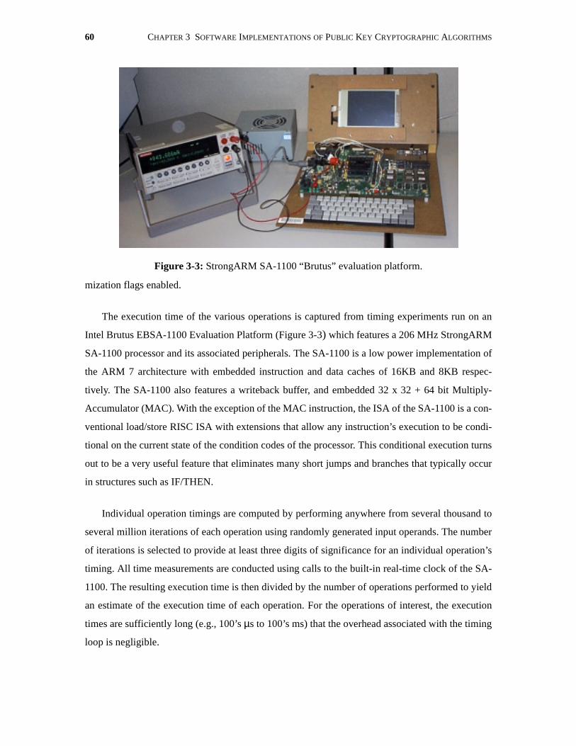
60 CHAPTER 3 SOFTWARE IMPLEMENTATIONS OF PUBLIC KEY CRYPTOGRAPHIC ALGORITHMS
mization flags enabled.
The execution time of the various operations is captured from timing experiments run on an
Intel Brutus EBSA-1100 Evaluation Platform (Figure 3-3) which features a 206 MHz StrongARM
SA-1100 processor and its associated peripherals. The SA-1100 is a low power implementation of
the ARM 7 architecture with embedded instruction and data caches of 16KB and 8KB respec-
tively. The SA-1100 also features a writeback buffer, and embedded 32 x 32 + 64 bit Multiply-
Accumulator (MAC). With the exception of the MAC instruction, the ISA of the SA-1100 is a con-
ventional load/store RISC ISA with extensions that allow any instruction’s execution to be condi-
tional on the current state of the condition codes of the processor. This conditional execution turns
out to be a very useful feature that eliminates many short jumps and branches that typically occur
in structures such as IF/THEN.
Individual operation timings are computed by performing anywhere from several thousand to
several million iterations of each operation using randomly generated input operands. The number
of iterations is selected to provide at least three digits of significance for an individual operation’s
timing. All time measurements are conducted using calls to the built-in real-time clock of the SA-
1100. The resulting execution time is then divided by the number of operations performed to yield
an estimate of the execution time of each operation. For the operations of interest, the execution
times are sufficiently long (e.g., 100’s µs to 100’s ms) that the overhead associated with the timing
loop is negligible.
Figure 3-3: StrongARM SA-1100 “Brutus” evaluation platform.

3.4 MULTI-PRECISION MODULAR INTEGER ARITHMETIC 61
The energy consumption of the various software operations is measured using the fact that
energy is the product of the operations’ execution time and the power consumption of the proces-
sor during execution. The execution time is measured using the methodology described in the pre-
ceeding paragraph. The processor’s power consumption is measured via a small modification to
the EBSA-1100 that allows the SA-1100’s core power supply to be isolated and driven by a Kei-
thley SourceMeter. The SourceMeter combines the functionality of a power supply and a multime-
ter such that it can be used as the voltage supply that powers the SA-1100 core, while providing a
readout of the current being drawn. Given the output voltage and current drawn one can compute
the power, which can be multiplied by the execution time to give the operation’s energy consump-
tion.
Both the instruction and data caches, as well as the write buffer are enabled to maximize per-
formance while minimizing the number of external memory references. Minimization of the exter-
nal memory references is crucial due to their large latencies and high energy consumptions. Note
that enabling the caches increases the power dissipation of the SA-1100 by approximately a factor
of 4, but the resulting reduction in execution time is on the order of 30-50x (Table 3-1). Hence, the
energy consumption of the processor actually decreases when the caches are enabled by approxi-
mately an order of magnitude.
3.4 Multi-precision Modular Integer ArithmeticThe operations required for implementing IF-based schemes, as well as DL and ECC-based
schemes over fields of odd prime characteristic are implemented over the multiplicative subgroup
of Zn, Zn*, where n is either the product of two primes, or a prime number itself (in which case it is
common to change the nomenclature to use p instead of n). The basic operations required for these
cryptographic schemes are modular addition, subtraction, multiplication, squaring, inversion, and
exponentiation.
The following subsections describe the development and implementation of the required
Execution Time (µs per operation)
64b 128b 192b 256b 320b 384b 448b 512b
w/o cache 359 536 734 956 1209 1434 1804 2143
w/cache 7.8 14 20 30.6 39.6 49.2 59.2 74
Table 3-1: Execution time for various sizes of modular squaring operationson StrongARM SA-1100 with caches enabled and disabled.

62 CHAPTER 3 SOFTWARE IMPLEMENTATIONS OF PUBLIC KEY CRYPTOGRAPHIC ALGORITHMS
multi-precision modular arithmetic package. Initially the basic non-modular arithmetic is
described, followed by a description of its modular forms. Optimizations are also proposed and
their effects on performance are quantified.
3.4.1 Notation
The notation that is used in this section follows that illustrated in Figure 3-1, and re-stated here for
convenience:
• A,B,C,...: multi-precision n-bit operands
• n: number of bits in the operand
• w: number of bits in the processors word-size (e.g., 32-bits for the StrongARM)
• k: number of bits used to represent each digit, given the StrongARM’s access to 64-bitwide products and accumulations, k can be chosen to be the full 32-bit width of the pro-cessor (i.e., k = w)
• m: number of words in the array used to store a multi-precision operand ( )
• A[i]: word i of the array used to store the multi-precision operand A (used in pseudo-code descriptions of functions)
• Ai: the ith digit of the base-2k representation of the multi-precision operand A (equiva-lent to A[i], used in mathematical formulae and illustrations)
• ai: the ith bit of the multi-precision operand A
• (x,y): denotes the concatenation of two variables of any type (used in assignments inwhich the result overflows a single variable such as the product of two words beingassigned to a double-word result, or the result of an adding two words being assigned toa word and carry-flag).
3.4.2 Addition/SubtractionMulti-precision addition and subtraction are performed using the standard pen-and-paper method
which utilizes digit-wise accumulation/subtraction. The resulting implementations are described in
ALG 3-1 and ALG 3-2.
Input: A,B: non-negative operands represented using m word arrayscin: a single bit representing the carry-in.
Output: P = A + B + cin, an m word arraycout = single bit carry-out
Algorithm: (carry, P[0]) = A[0] + B[0] + cinfor (i = 1; i < m; i = i + 1)
(carry, P[i]) = A[i] + B[i] + carryendforcout = carry
Algorithm 3-1: Multi-precision addition.
m n k⁄=
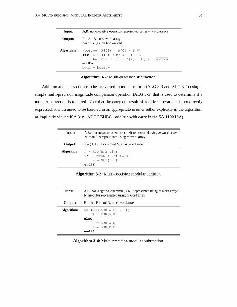
3.4 MULTI-PRECISION MODULAR INTEGER ARITHMETIC 63
Addition and subtraction can be converted to modular form (ALG 3-3 and ALG 3-4) using a
simple multi-precision magnitude comparison operation (ALG 3-5) that is used to determine if a
modulo-correction is required. Note that the carry-out result of addition operations is not directly
expressed; it is assumed to be handled in an appropriate manner either explicitly in the algorithm,
or implicitly via the ISA (e.g., ADDC/SUBC - add/sub with carry in the SA-1100 ISA).
Input: A,B: non-negative operands represented using m word arrays
Output: P = A - B, an m word arraybout = single bit borrow-out
Algorithm: (borrow, P[0]) = A[0] - B[0]for (i = 1; i < m; i = i + 1)
(borrow, P[i]) = A[i] - B[i] - borrowendforbout = borrow
Algorithm 3-2: Multi-precision subtraction.
Input: A,B: non-negative operands (< N) represented using m word arraysN: modulus represented using m word array
Output: P = (A + B + cin) mod N, an m word array
Algorithm: P = ADD(A,B,cin)if (COMPARE(P,N) >= 0)
P = SUB(P,N)endif
Algorithm 3-3: Multi-precision modular addition.
Input: A,B: non-negative operands (< N), represented using m word arraysN: modulus represented using m word array
Output: P = (A - B) mod N, an m word array
Algorithm: if (COMPARE(A,B) >= 0)P = SUB(A,B)
elseP = ADD(A,N)P = SUB(P,B)
endif
Algorithm 3-4: Multi-precision modular subtraction.

64 CHAPTER 3 SOFTWARE IMPLEMENTATIONS OF PUBLIC KEY CRYPTOGRAPHIC ALGORITHMS
3.4.3 Integer Multiplication and Squaring
In its simplest form, multiplication/squaring requires O(m2) single-precision multiplications which
can become quite inefficient as the number of words per operand increases to 16 or 32. The basic
multiplication operation is illustrated in Figure 3-4(a) for m = 2, and the general case is described
in ALG 3-6. Essentially, each word of the multiplicand (i.e., Bj) is multiplied by each word of the
multiplier (i.e., Ai), generating a word-pair denoted as (C,S). The resulting double-word product
terms are then aligned appropriately and accumulated to yield the final answer.
Input: A,B: non-negative operands represented using m word arrays
Output: P =
Algorithm: for (i = m - 1; i >= 0; i = i - 1)if (A[i] > B[i])
return(1)elseif (A[i] < B[i])
return(-1)endif
endforreturn(0)
Algorithm 3-5: Multi-precision magnitude comparison.
Input: A,B: non-negative operands represented using m word arrays
Output: P = A·B, a 2m word product
Algorithm: clear Pfor (i = 0; i < m; i = i + 1)
C = 0for (j = 0; j < m; j = j + 1)
(C, S) = A[i]·B[j] + P[i+j] + CP[i+j] = S
endforendforP[2m-1] = C
Algorithm 3-6: Multi-precision integer multiplication.
sign A B–( ) 1 0,±{ }∈
Figure 3-4: Multi-precision multiplication/squaring examples.
B1 B0
A1 A0
A0B0
A0B1
A1B0
A1B1
A x B
A1 A0
A1 A0
A02
2·A0A1
A12
A2
4 single precisionmultiplications
3 single precisionmultiplications
5 single precisionadditions
3 single precisionadditions
1 shift operation
(a) (b)
multiplier
multiplicand
multiplier
multiplicand
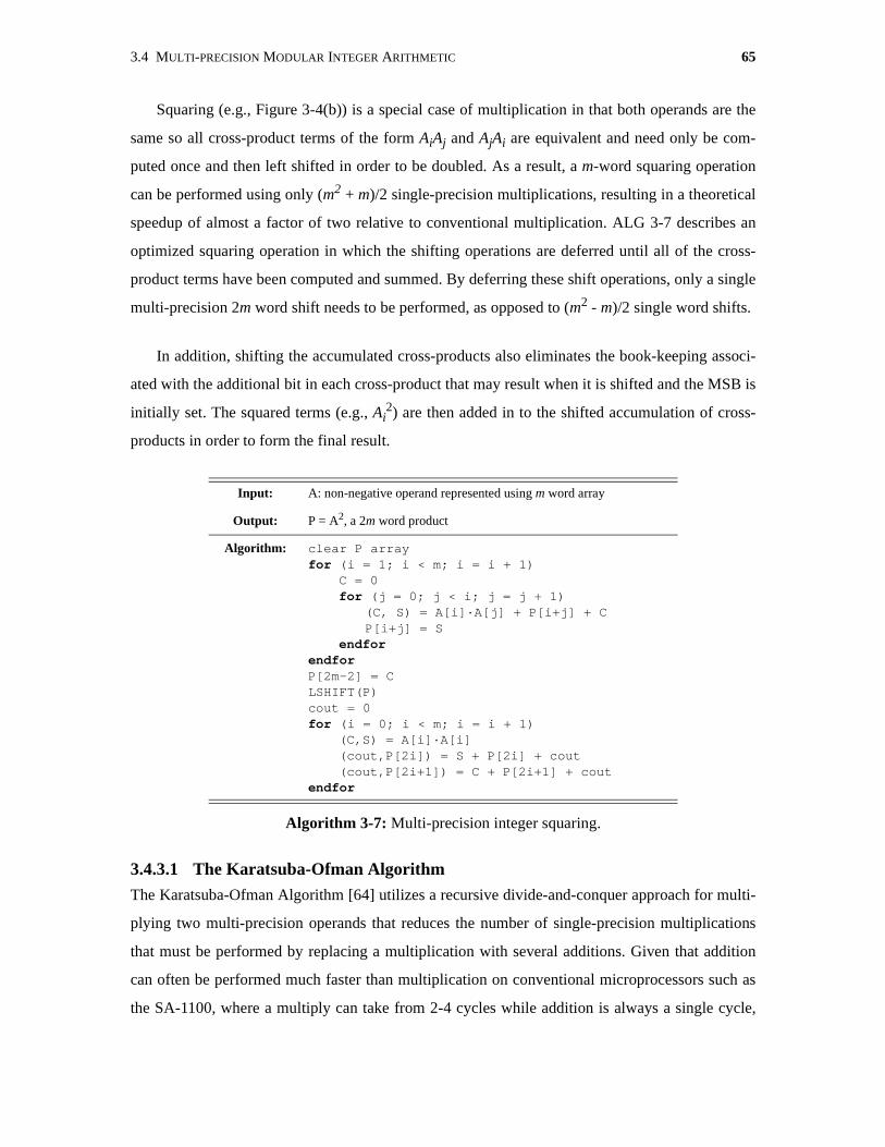
3.4 MULTI-PRECISION MODULAR INTEGER ARITHMETIC 65
Squaring (e.g., Figure 3-4(b)) is a special case of multiplication in that both operands are the
same so all cross-product terms of the form AiAj and AjAi are equivalent and need only be com-
puted once and then left shifted in order to be doubled. As a result, a m-word squaring operation
can be performed using only (m2 + m)/2 single-precision multiplications, resulting in a theoretical
speedup of almost a factor of two relative to conventional multiplication. ALG 3-7 describes an
optimized squaring operation in which the shifting operations are deferred until all of the cross-
product terms have been computed and summed. By deferring these shift operations, only a single
multi-precision 2m word shift needs to be performed, as opposed to (m2 - m)/2 single word shifts.
In addition, shifting the accumulated cross-products also eliminates the book-keeping associ-
ated with the additional bit in each cross-product that may result when it is shifted and the MSB is
initially set. The squared terms (e.g., Ai2) are then added in to the shifted accumulation of cross-
products in order to form the final result.
3.4.3.1 The Karatsuba-Ofman Algorithm
The Karatsuba-Ofman Algorithm [64] utilizes a recursive divide-and-conquer approach for multi-
plying two multi-precision operands that reduces the number of single-precision multiplications
that must be performed by replacing a multiplication with several additions. Given that addition
can often be performed much faster than multiplication on conventional microprocessors such as
the SA-1100, where a multiply can take from 2-4 cycles while addition is always a single cycle,
Input: A: non-negative operand represented using m word array
Output: P = A2, a 2m word product
Algorithm: clear P arrayfor (i = 1; i < m; i = i + 1)
C = 0for (j = 0; j < i; j = j + 1)
(C, S) = A[i]·A[j] + P[i+j] + CP[i+j] = S
endforendforP[2m-2] = CLSHIFT(P)cout = 0for (i = 0; i < m; i = i + 1)
(C,S) = A[i]·A[i](cout,P[2i]) = S + P[2i] + cout(cout,P[2i+1]) = C + P[2i+1] + cout
endfor
Algorithm 3-7: Multi-precision integer squaring.

66 CHAPTER 3 SOFTWARE IMPLEMENTATIONS OF PUBLIC KEY CRYPTOGRAPHIC ALGORITHMS
the net result is an improvement in performance.
Karatsuba’s algorithm computes the product A·B given two n-bit operands which we assume
can be partitioned into two n/2-bit halves: A = Ah·2n/2 + Al, B = Bh·2n/2 + Bl. The product A·B is
computed using the three product values t0 = AhBh, t1 = AlBl, and t2 = (Ah+Al)(Bh+Bl), which are
combined as follows:
(3-1)
EQ 3-1 computes a n-bit multiplication using two n/2-bit multiplications, one (n/2 + 1)-bit
multiplication to handle the product-of-sum term, and several multi-precision additions. The
resulting n/2 and (n/2 + 1) bit multiplications can in turn be computed using Karatsuba’s algorithm
again, leading to a recursive multiplication algorithm that asymptotically approaches a minimum
number of O( ) single-precision multiplications. In practice, the number of levels of recursion
that are used will ultimately be dictated by the amount of overhead associated with a particular
implementation of the algorithm, and the relative performance of the multiplication and addition
operations (the slower the multiplier, the more recursion that should be used). In some implemen-
tations the extra bit required for the product-of-sum term may introduce difficulties/inefficiencies
that can be overcome by using an alternative implementation that utilizes the product-of-differ-
ences t2 = (Ah-Al)·(Bh-Bl):
(3-2)
Note that care must be taken to deal with the possibility of negative differences in EQ 3-2.
The basic 2-way divide-and-conquer approach used by the Karatsuba-Ofman algorithm can be
extended to m-way partitioning to yield even lower asymptotic complexities [143] on the order of
O( ). However, in practice the overhead of these schemes outweighs any of the perfor-
mance benefits so further partitioning is rarely, if ever, used.
A B⋅ t0 2n
t2 t0– t1–( ) 2n 2⁄
t1+⋅+⋅AhBh( )2
nAh Al+( ) Bh Bl+( ) AhBh– AlBl–( )2
n 2⁄AlBl( )+ +
AhBh( )2n
AhBh AhBl AlBh AlBl AhBh– AlBl–+ + +( )2n 2⁄
AlBl( )+ +
AhBh( )2n
AhBl AlBh+( )2n 2⁄
AlBl( )+ +
=
=
=
=
n32log
A B⋅ t0 2n
t0 t1 t2–+( )2n 2⁄
t1+ +⋅AhBh( )2
nAhBh AlBl Ah Al–( ) Bh Bl–( )⋅–+( )2
n 2⁄AlBl( )+ +
AhBh( )2n
AhBh AlBl AhBh– AlBl– AhBl AlBh+ + +( )2n 2⁄
AlBl( )+ +
AhBh( )2n
AhBl AlBh+( )2n 2⁄
AlBl( )+ +
=
=
=
=
n2m 1–( )mlog
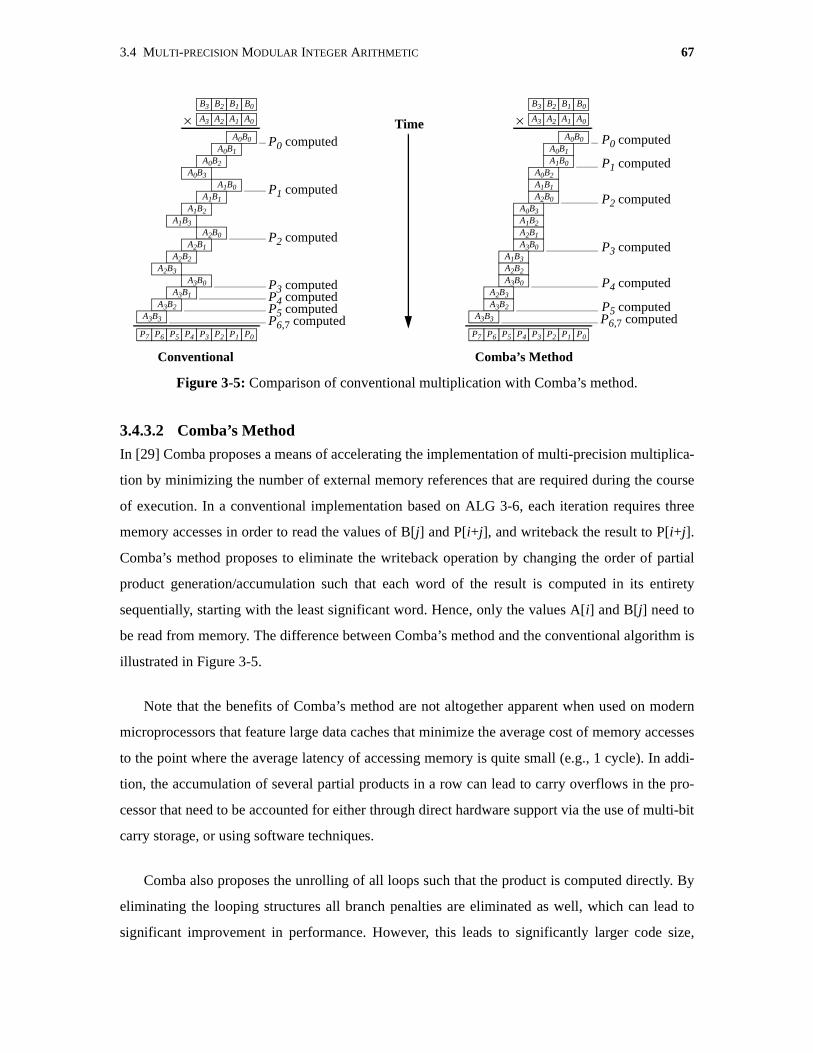
3.4 MULTI-PRECISION MODULAR INTEGER ARITHMETIC 67
3.4.3.2 Comba’s Method
In [29] Comba proposes a means of accelerating the implementation of multi-precision multiplica-
tion by minimizing the number of external memory references that are required during the course
of execution. In a conventional implementation based on ALG 3-6, each iteration requires three
memory accesses in order to read the values of B[j] and P[i+j], and writeback the result to P[i+j].
Comba’s method proposes to eliminate the writeback operation by changing the order of partial
product generation/accumulation such that each word of the result is computed in its entirety
sequentially, starting with the least significant word. Hence, only the values A[i] and B[j] need to
be read from memory. The difference between Comba’s method and the conventional algorithm is
illustrated in Figure 3-5.
Note that the benefits of Comba’s method are not altogether apparent when used on modern
microprocessors that feature large data caches that minimize the average cost of memory accesses
to the point where the average latency of accessing memory is quite small (e.g., 1 cycle). In addi-
tion, the accumulation of several partial products in a row can lead to carry overflows in the pro-
cessor that need to be accounted for either through direct hardware support via the use of multi-bit
carry storage, or using software techniques.
Comba also proposes the unrolling of all loops such that the product is computed directly. By
eliminating the looping structures all branch penalties are eliminated as well, which can lead to
significant improvement in performance. However, this leads to significantly larger code size,
Figure 3-5: Comparison of conventional multiplication with Comba’s method.
B0B1B2B3
A0A1A2A3
A0B0 A0B1
A0B2A0B3
A1B0 A1B1
A1B2A1B3
A2B0 A2B1
A2B2A2B3
A3B0 A3B1
A3B2A3B3
P4P5P6P7 P0P1P2P3
Time
B0B1B2B3
A0A1A2A3
A0B0 A0B1A1B0
A0B2A1B1 A2B0
A0B3A1B2 A2B1 A3B0
A1B3A2B2 A3B0
A2B3A3B2
A3B3
P4P5P6P7 P0P1P2P3
P0 computed
P1 computed
P2 computed
P3 computedP4 computedP5 computedP6,7 computed
P0 computed
P1 computed
P2 computed
P3 computed
P4 computed
P5 computedP6,7 computed
Conventional Comba’s Method
68 CHAPTER 3 SOFTWARE IMPLEMENTATIONS OF PUBLIC KEY CRYPTOGRAPHIC ALGORITHMS
which scales quadratically with operand size, and requires explicit multiplication routines for each
possible size of operands. Hence, a trade-off must be made between code size and performance
requirements to determine whether or not loop unrolling is feasible.
Significant performance benefits can be achieved by combining Comba’s Method with the
Karatsuba-Ofman algorithm. The resulting hybrid scheme utilizes the Karatsuba-Ofman algorithm
to decompose large (e.g., 1024-bit) multiplications into much smaller ones (e.g., 256-bit) that are
then performed using Comba’s Method with loop unrolling. The resulting implementation is on
average approximately 50% faster than the conventional approach of ALG 3-6 (Table 3-2).
3.4.3.3 Fast Fourier Transform (FFT) Based MultiplicationThe fastest algorithms for performing multi-precision integer multiplication are attributed to tech-
niques based on the FFT [97]. By interpreting multi-precision integers as polynomials with the
indeterminate x = 2w (i.e., the word-size of the processor), long integer multiplications become
simple convolutions for which the FFT is ideally suited. The net result is a multiplication algo-
rithm with complexity O(n·log n·loglog n). Unfortunately, the high degree of overhead associated
with FFT-based approaches only makes them feasible for operands on the order of several thou-
sand bits long. Hence, they are not commonly used in asymmetric cryptography implementations
such as the work described by this dissertation. Readers are referred to Knuth’s excellent discus-
sion on FFT-based multiplication algorithms in [64] for further details.
3.4.4 Integer DivisionDivision is by far the most difficult multi-precision integer operation to perform efficiently as there
is no inherent support for integer division on most GPP’s such as the StrongARM. In some cases a
floating point divider may be exploited to provide very good performance, but no such device
exists on the SA-1100. Conventional multi-precision division algorithms are equivalent to the pen-
and-paper long division method taught in school in which multiples of the divisor are subtracted
from the dividend repeatedly until its value is reduced to less than that of the divisor, at which
point the division is complete, and the remaining dividend value is the remainder. The quotient is
Execution Time (µs per operation)
Method 128b 256b 512b 1024b
Conventional 1.7 5.3 18.9 72.2
Hybrid 0.94 3.1 15 54.6
Table 3-2: Comparison of execution times of conventional and optimized hybridComba/Karatsuba-Ofman multiplication implementations on StrongARM SA-1100.

3.4 MULTI-PRECISION MODULAR INTEGER ARITHMETIC 69
formed by keeping track of the multiplier values used to reduce the dividend with the divisor. This
simple technique is illustrated in Figure 3-6.
The division algorithm that is used within this dissertation features a slight modification of the
conventional pen-and-paper method shown in Figure 3-6 in that each quotient digit, which in this
case is a processor word, is initially an underestimate of the actual quotient digit which must in
turn be corrected. An estimate is used to improve performance as it only requires performing a 2-
word by 1-word division. Underestimating the quotient simplifies the correction procedure as we
know that the estimate can only ever increase, it will never decrease. Underestimating also ensures
that the reduced dividend is always non-negative, thus eliminating the book-keeping associated
with keeping track of its sign.
The performance of the resulting integer division algorithm can be improved through the use
of normalization. Normalization is essentially a left-shifting of the divisor and dividend to ensure
that the most significant word (MSW) of the divisor has its MSB set. Normalization allows more
accurate quotient estimation which reduces the number of corrections that need to be performed,
thus speeding up the division operation. Note that normalization doesn’t affect the quotient as both
divisor and dividend are scaled so their ratio will remain unaffected. However, the remainder must
be de-normalized by right-shifting its value by the appropriate amount. The final implementation
of the division algorithm is shown in ALG 3-8.
3.4.5 Modular Reduction and Montgomery’s MethodModular reduction can be performed using either conventional integer division (ALG 3-8), or an
Figure 3-6: Conventional multi-precision integer division example.
B0B1B2B3B4B5B6B7A0A1A2A3
P0P1P2P3P4
R0R1R2R3 B2
P0P1P2P3P4
B1R0R1R2R3
P0P1P2P3P4
R0R1R2R3 B0
P0P1P2P3P4
R0R1R2R3
D0D1D2D3
P = D3·A
P = D2·A
P = D1·A
P = D0·A
R = B7:3 - P
R = (R, B2) - P
R = (R, B1) - P
R = (R, B0) - P
B = D·A + R
D3 = B7:3 / A
D2 = (R, B2) / A
D1 = (R, B1) / A
D0 = (R, B0) / A
divisor dividend
quotient
remainder
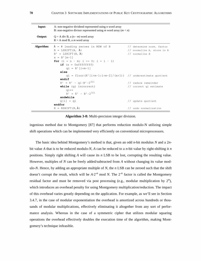
70 CHAPTER 3 SOFTWARE IMPLEMENTATIONS OF PUBLIC KEY CRYPTOGRAPHIC ALGORITHMS
ingenious method due to Montgomery [87] that performs reduction modulo-N utilizing simple
shift operations which can be implemented very efficiently on conventional microprocessors.
The basic idea behind Montgomery’s method is that, given an odd n-bit modulus N and a 2n-
bit value A that is to be reduced modulo-N, A can be reduced to a n-bit value by right-shifting it n
positions. Simply right shifting A will cause its n LSB to be lost, corrupting the resulting value.
However, multiples of N can be freely added/subtracted from A without changing its value mod-
ulo-N. Hence, by adding an appropriate multiple of N, the n LSB can be zeroed such that the shift
doesn’t corrupt the result, which will be A·2-n mod N. The 2-n factor is called the Montgomery
residual factor and must be removed via post processing (e.g., modular multiplication by 2n),
which introduces an overhead penalty for using Montgomery multiplication/reduction. The impact
of this overhead varies greatly depending on the application. For example, as we’ll see in Section
3.4.7, in the case of modular exponentiation the overhead is amortized across hundreds or thou-
sands of modular multiplications, effectively eliminating it altogether from any sort of perfor-
mance analysis. Whereas in the case of a symmetric cipher that utilizes modular squaring
operations the overhead effectively doubles the execution time of the algorithm, making Mont-
gomery’s technique infeasible.
Input: A: non-negative dividend represented using n word arrayB: non-negative divisor represented using m word array (m < n)
Output: Q = A div B, a (n - m) word arrayR = A mod B, a m word array
Algorithm: λ = # leading zeroes in MSW of BR = LSHIFT(A, λ)B’ = LSHIFT(B, λ)x = B’[m-1]for (i = n - m; i >= 0; i = i - 1)
if (x = 0xffffffff)qi = B’[i+m-1]
elseqi = floor(R’[i+m-1:i+m-2]/(x+1))
endifR’ = R’ - qi·B’·232i
while (qi incorrect)qi++R’ = R’ - B’·232i
endwhileQ[i] = qi
endforR = RSHIFT(R,λ)
// determine norm. factor// normalize A, store in R// normalize B
// underestimate quotient
// reduce remainder// correct qi estimate
// update quotient
// undo normalization
Algorithm 3-8: Multi-precision integer division.
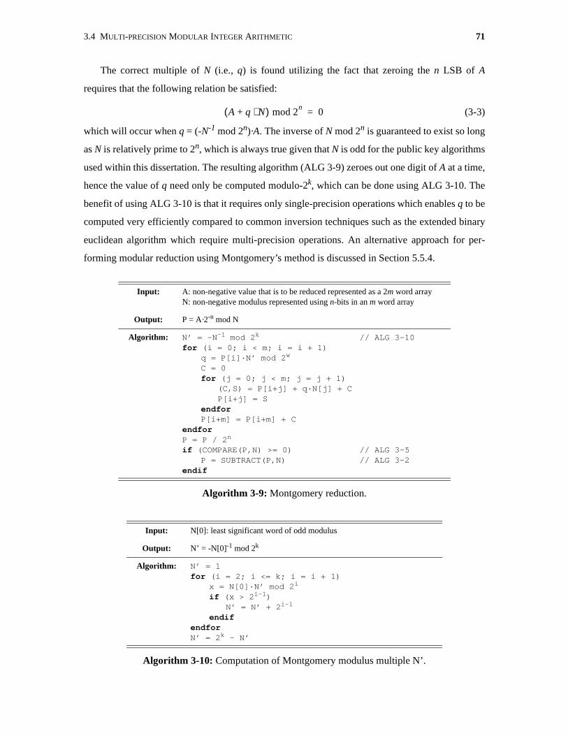
3.4 MULTI-PRECISION MODULAR INTEGER ARITHMETIC 71
The correct multiple of N (i.e., q) is found utilizing the fact that zeroing the n LSB of A
requires that the following relation be satisfied:
(3-3)
which will occur when q = (-N-1 mod 2n)·A. The inverse of N mod 2n is guaranteed to exist so long
as N is relatively prime to 2n, which is always true given that N is odd for the public key algorithms
used within this dissertation. The resulting algorithm (ALG 3-9) zeroes out one digit of A at a time,
hence the value of q need only be computed modulo-2k, which can be done using ALG 3-10. The
benefit of using ALG 3-10 is that it requires only single-precision operations which enables q to be
computed very efficiently compared to common inversion techniques such as the extended binary
euclidean algorithm which require multi-precision operations. An alternative approach for per-
forming modular reduction using Montgomery’s method is discussed in Section 5.5.4.
Input: A: non-negative value that is to be reduced represented as a 2m word arrayN: non-negative modulus represented using n-bits in an m word array
Output: P = A·2-n mod N
Algorithm: N’ = -N-1 mod 2k
for (i = 0; i < m; i = i + 1)q = P[i]·N’ mod 2w
C = 0for (j = 0; j < m; j = j + 1)
(C,S) = P[i+j] + q·N[j] + CP[i+j] = S
endforP[i+m] = P[i+m] + C
endforP = P / 2n
if (COMPARE(P,N) >= 0)P = SUBTRACT(P,N)
endif
// ALG 3-10
// ALG 3-5// ALG 3-2
Algorithm 3-9: Montgomery reduction.
Input: N[0]: least significant word of odd modulus
Output: N’ = -N[0]-1 mod 2k
Algorithm: N’ = 1for (i = 2; i <= k; i = i + 1)
x = N[0]·N’ mod 2i
if (x > 2i-1)N’ = N’ + 2i-1
endifendforN’ = 2k - N’
Algorithm 3-10: Computation of Montgomery modulus multiple N’.
A q N⋅+( ) mod 2n
0=
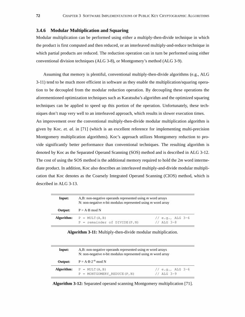
72 CHAPTER 3 SOFTWARE IMPLEMENTATIONS OF PUBLIC KEY CRYPTOGRAPHIC ALGORITHMS
3.4.6 Modular Multiplication and SquaringModular multiplication can be performed using either a multiply-then-divide technique in which
the product is first computed and then reduced, or an interleaved multiply-and-reduce technique in
which partial products are reduced. The reduction operation can in turn be performed using either
conventional division techniques (ALG 3-8), or Montgomery’s method (ALG 3-9).
Assuming that memory is plentiful, conventional multiply-then-divide algorithms (e.g., ALG
3-11) tend to be much more efficient in software as they enable the multiplication/squaring opera-
tion to be decoupled from the modular reduction operation. By decoupling these operations the
aforementioned optimization techniques such as Karatsuba’s algorithm and the optimized squaring
techniques can be applied to speed up this portion of the operation. Unfortunately, these tech-
niques don’t map very well to an interleaved approach, which results in slower execution times.
An improvement over the conventional multiply-then-divide modular multiplication algorithm is
given by Koc. et. al. in [71] (which is an excellent reference for implementing multi-precision
Montgomery multiplication algorithms). Koc’s approach utilizes Montgomery reduction to pro-
vide significantly better performance than conventional techniques. The resulting algorithm is
denoted by Koc as the Separated Operand Scanning (SOS) method and is described in ALG 3-12.
The cost of using the SOS method is the additional memory required to hold the 2m word interme-
diate product. In addition, Koc also describes an interleaved multiply-and-divide modular multipli-
cation that Koc denotes as the Coarsely Integrated Operand Scanning (CIOS) method, which is
described in ALG 3-13.
Input: A,B: non-negative operands represented using m word arraysN: non-negative n-bit modulus represented using m word array
Output: P = A·B mod N
Algorithm: P = MULT(A,B)P = remainder of DIVIDE(P,N)
// e.g., ALG 3-6// ALG 3-8
Algorithm 3-11: Multiply-then-divide modular multiplication.
Input: A,B: non-negative operands represented using m word arraysN: non-negative n-bit modulus represented using m word array
Output: P = A·B·2-n mod N
Algorithm: P = MULT(A,B)P = MONTGOMERY_REDUCE(P,N)
// e.g., ALG 3-6// ALG 3-9
Algorithm 3-12: Separated operand scanning Montgomery multiplication [71].
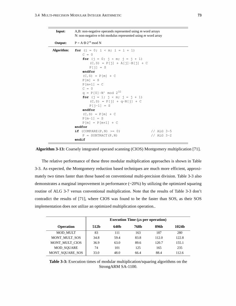
3.4 MULTI-PRECISION MODULAR INTEGER ARITHMETIC 73
The relative performance of these three modular multiplication approaches is shown in Table
3-3. As expected, the Montgomery reduction based techniques are much more efficient, approxi-
mately two times faster than those based on conventional multi-precision division. Table 3-3 also
demonstrates a marginal improvement in performance (~20%) by utilizing the optimized squaring
routine of ALG 3-7 versus conventional multiplication. Note that the results of Table 3-3 don’t
contradict the results of [71], where CIOS was found to be the faster than SOS, as their SOS
implementation does not utilize an optimized multiplication operation..
Input: A,B: non-negative operands represented using m word arraysN: non-negative n-bit modulus represented using m word array
Output: P = A·B·2-n mod N
Algorithm: for (i = 0; i < m; i = i + 1)C = 0for (j = 0; j < m; j = j + 1)
(C,S) = P[j] + A[j]·B[j] + CP[j] = S
endfor(C,S) = P[m] + CP[m] = SP[m+1] = CC = 0q = P[0]·N’ mod 232
for (j = 1; j < m; j = j + 1)(C,S) = P[j] + q·N[j] + CP[j-1] = S
endfor(C,S) = P[m] + CP[m-1] = SP[m] = P[m+1] + C
endforif (COMPARE(P,N) >= 0)
P = SUBTRACT(P,N)endif
// ALG 3-5// ALG 3-2
Algorithm 3-13: Coarsely integrated operand scanning (CIOS) Montgomery multiplication [71].
Execution Time (µs per operation)
Operation 512b 640b 768b 896b 1024b
MOD_MULT 83 111 163 187 280
MONT_MULT_SOS 34.8 59.4 83.8 112.0 122.8
MONT_MULT_CIOS 36.9 63.0 89.6 120.7 155.1
MOD_SQUARE 74 101 125 165 235
MONT_SQUARE_SOS 33.0 48.0 66.4 88.4 112.6
Table 3-3: Execution times of modular multiplication/squaring algorithms on theStrongARM SA-1100.

74 CHAPTER 3 SOFTWARE IMPLEMENTATIONS OF PUBLIC KEY CRYPTOGRAPHIC ALGORITHMS
3.4.7 Modular ExponentiationModular exponentiation is the basic cryptographic primitive for both IF and DL-based cryptosys-
tems. As such, there has been a large amount of research devoted to various optimization tech-
niques for improving the performance of modular exponentiation. The simplest of these technique
is known as the binary modular exponentiation method. The binary method computes AE mod N
using the binary expansion of the exponent E = (en-1, en-2, ... , e1, e0), and a repeated square-and-
multiply operation to compute the required result using ALG 3-14, which requires on average n/2
modular multiplies and n modular squarings.
The binary method can be improved by scanning the exponent r = log2m bits at a time and
using pre-computed powers of A to reduce the number of required modular multiplications. The
resulting m-ary method (ALG 3-15) requires (2r - 2) modular multiplications for the pre-comput-
ing the powers of A, (n - r) modular squaring operations, and on average (1 - 2-r)(n/r - 1) modular
multiplications. The reduction in the number of multiplications is due to the fact that no multipli-
cation is required if ei = 0, which occurs with probability 2-r assuming the exponent bits are uni-
formly distributed with probability 1/2. Depending on the size of the exponent and the amount of
memory that is available for storing pre-computed values, an optimal value of r can be determined
via experimentation (e.g., ropt = 5 for 1024-bit exponentiation using the implementation developed
for this dissertation).
Other more complex exponentiation techniques such as addition chains ([64], page 465-485)
and both constant and variable-width non-zero sliding windows can also be utilized. However,
they were not utilized in the modular integer arithmetic package described within this dissertation.
For further discussion of these, and other exponentiation techniques, the reader is referred to either
Input: A: non-negative operand represented using m word arraysE: non-negative n-bit exponent represented as (en-1, en-2, . . . , e1, e0)N: non-negative n-bit modulus represented using m word array
Output: P = AE mod N
Algorithm: P = 1for (i = n - 1; i >= 0; i = i - 1)
P = MOD_SQUARE(P,N)if (ei == 1)
P = MOD_MULT(P,A,N)endif
endfor
// P = P2
// P = P·
Algorithm 3-14: Binary method for modular exponentiation.
Aei

3.4 MULTI-PRECISION MODULAR INTEGER ARITHMETIC 75
Gordon’s excellent overview of exponentiation methods [51], or RSA Lab’s comprehensive,
though somewhat dated, guide to fast RSA software implementation [68].
The performance benefits of utilizing Montgomery multiplication and squaring becomes very
apparent when these techniques are applied to modular exponentiation, yielding approximately a
2x performance improvement (Table 3-4). However, when using Montgomery multiplication/
squaring, care must be taken to account for the Montgomery residual factor of 2-n that is intro-
Input: A: non-negative operandE: non-negative n-bit exponent represented as a sequence of r-bit digits
(ek-1, ek-2, . . . , e1, e0), where m = 2r
N: non-negative n-bit modulus
Output: P = AE mod N
Algorithm: for (i = 2; i < m; i = i + 1)pre-compute and store Ai
endforP = mod Nfor (i = k - 2; i >= 0; i = i - 1)
P = MOD_SQUARE(P,N)...P = MOD_SQUARE(P,N)if (ei > 0)
P = MOD_MULT(P, ,N)endif
endfor
// repeat until // is // computed
// P = P·
Algorithm 3-15: m-ary method for modular exponentiation.
Input: A: non-negative operandE: non-negative n-bit exponent represented as a sequence of r-bit digits
(ek-1, ek-2, . . . , e1, e0)N: non-negative n-bit modulus
Output: P = AE mod N
Algorithm: A = MOD_MULT(A,2n,N)for (i = 2; i < m; i = i + 1)
pre-compute and store Ai·2n
endforP = Aek-1·2n mod Nfor (i = k - 2; i >= 0; i = i - 1)
P = MONT_SQUARE(P,N)...P = MONT_SQUARE(P,N)if (ei > 0)
P = MONT_MULT(P,Aei,N)endif
endforP = MONT_REDUCE(P,N)
A = A·2n mod N
// repeat until // Pr is // computed
// P = AE·2n mod N// P = AE mod N
Algorithm 3-16: m-ary Montgomery exponentiation.
Aek 1–
Aei
Pm
P2r
=
Aei
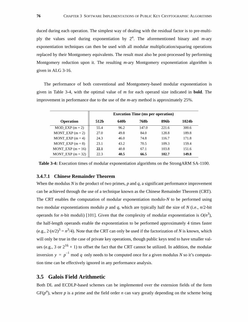
76 CHAPTER 3 SOFTWARE IMPLEMENTATIONS OF PUBLIC KEY CRYPTOGRAPHIC ALGORITHMS
duced during each operation. The simplest way of dealing with the residual factor is to pre-multi-
ply the values used during exponentiation by 2n. The aforementioned binary and m-ary
exponentiation techniques can then be used with all modular multiplication/squaring operations
replaced by their Montgomery equivalents. The result must also be post-processed by performing
Montgomery reduction upon it. The resulting m-ary Montgomery exponentiation algorithm is
given in ALG 3-16.
The performance of both conventional and Montgomery-based modular exponentiation is
given in Table 3-4, with the optimal value of m for each operand size indicated in bold. The
improvement in performance due to the use of the m-ary method is approximately 25%.
3.4.7.1 Chinese Remainder TheoremWhen the modulus N is the product of two primes, p and q, a significant performance improvement
can be achieved through the use of a technique known as the Chinese Remainder Theorem (CRT).
The CRT enables the computation of modular exponentiation modulo-N to be performed using
two modular exponentiations modulo p and q, which are typically half the size of N (i.e., n/2-bit
operands for n-bit moduli) [101]. Given that the complexity of modular exponentiation is O(n3),
the half-length operands enable the exponentiation to be performed approximately 4 times faster
(e.g., 2·(n/2)3 = n3/4). Note that the CRT can only be used if the factorization of N is known, which
will only be true in the case of private key operations, though public keys tend to have smaller val-
ues (e.g., 3 or 216 + 1) to offset the fact that the CRT cannot be utilized. In addition, the modular
inversion only needs to be computed once for a given modulus N so it’s computa-
tion time can be effectively ignored in any performance analysis.
3.5 Galois Field ArithmeticBoth DL and ECDLP-based schemes can be implemented over the extension fields of the form
GF(pn), where p is a prime and the field order n can vary greatly depending on the scheme being
Execution Time (ms per operation)
Operation 512b 640b 768b 896b 1024b
MOD_EXP (m = 2) 55.4 96.2 147.0 221.6 300.6
MONT_EXP (m = 2) 27.0 49.8 84.0 128.8 189.8
MONT_EXP (m = 4) 24.3 46.0 74.8 116.7 171.8
MONT_EXP (m = 8) 23.1 43.2 70.5 109.3 159.4
MONT_EXP (m = 16) 22.1 40.8 67.1 103.8 151.6
MONT_EXP (m = 32) 22.3 40.5 66.5 102.7 149.8
Table 3-4: Execution times of modular exponentiation algorithms on the StrongARM SA-1100.
y p1– mod q=
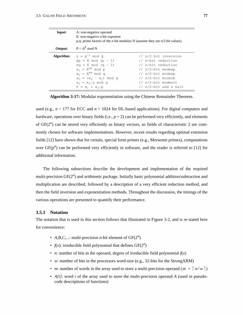
3.5 GALOIS FIELD ARITHMETIC 77
used (e.g., n ~ 177 for ECC and n > 1024 for DL-based applications). For digital computers and
hardware, operations over binary fields (i.e., p = 2) can be performed very efficiently, and elements
of GF(2n) can be stored very efficiently as binary vectors, so fields of characteristic 2 are com-
monly chosen for software implementations. However, recent results regarding optimal extension
fields [12] have shown that for certain, special form primes (e.g., Mersenne primes), computations
over GF(pn) can be performed very efficiently in software, and the reader is referred to [12] for
additional information.
The following subsections describe the development and implementation of the required
multi-precision GF(2n) and arithmetic package. Initially basic polynomial addition/subtraction and
multiplication are described, followed by a description of a very efficient reduction method, and
then the field inversion and exponentiation methods. Throughout the discussion, the timings of the
various operations are presented to quantify their performance.
3.5.1 Notation
The notation that is used in this section follows that illustrated in Figure 3-2, and is re-stated here
for convenience:
• A,B,C,...: multi-precision n-bit element of GF(2n)
• f(x): irreducible field polynomial that defines GF(2n)
• n: number of bits in the operand, degree of irreducible field polynomial f(x)
• w: number of bits in the processors word-size (e.g., 32-bits for the StrongARM)
• m: number of words in the array used to store a multi-precision operand ( )
• A[i]: word i of the array used to store the multi-precision operand A (used in pseudo-code descriptions of functions)
Input: A: non-negative operandE: non-negative n-bit exponent p,q: prime factors of the n-bit modulus N (assume they are n/2-bit values)
Output: P = AE mod N
Algorithm: y = p-1 mod qep = E mod (p - 1)eq = E mod (q - 1)x1 = A
ep mod px2 = A
eq mod qx3 = (x2 - x1) mod qx3 = x3·y mod qP = x1 + x3·p
// n/2 bit inversion// n-bit reduction// n-bit reduction// n/2-bit modexp// n/2-bit modexp// n/2-bit modsub// n/2-bit modmult// n/2-bit add & mult
Algorithm 3-17: Modular exponentiation using the Chinese Remainder Theorem.
m n w⁄=
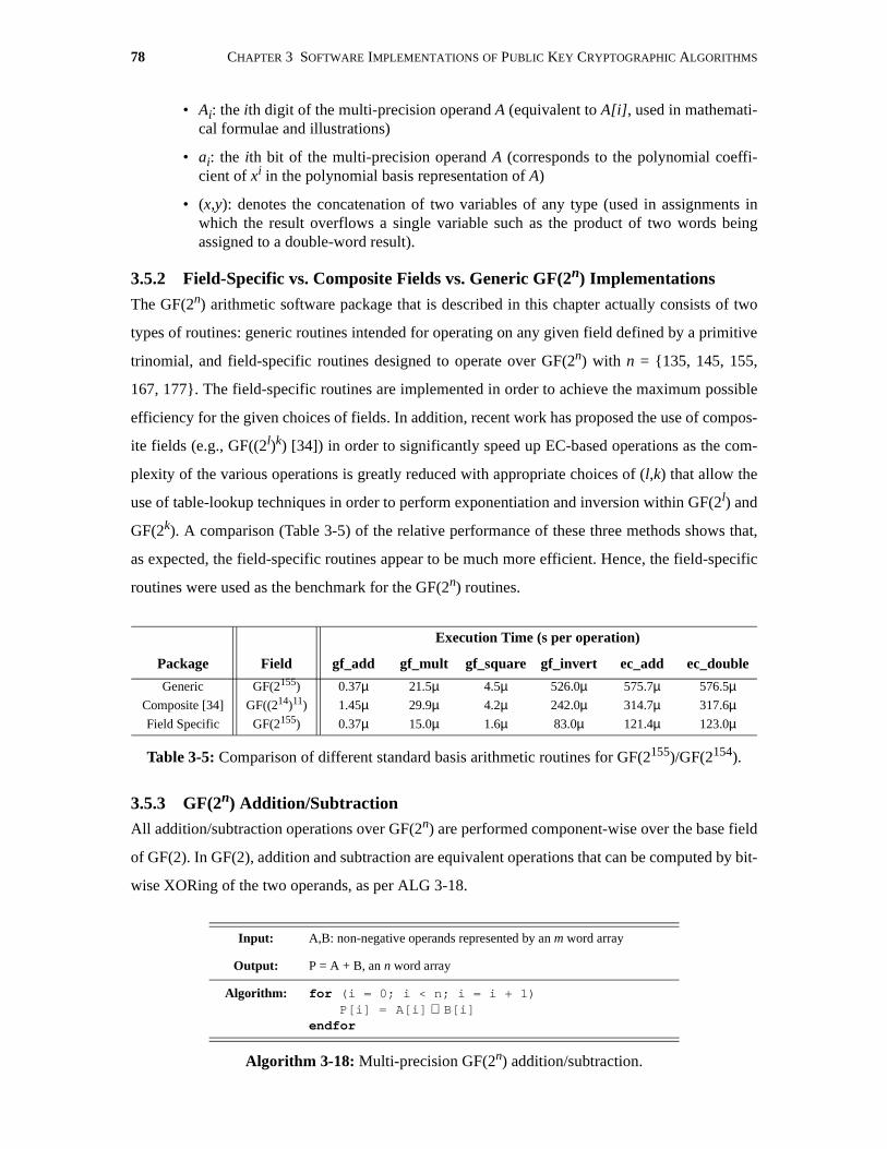
78 CHAPTER 3 SOFTWARE IMPLEMENTATIONS OF PUBLIC KEY CRYPTOGRAPHIC ALGORITHMS
• Ai: the ith digit of the multi-precision operand A (equivalent to A[i], used in mathemati-cal formulae and illustrations)
• ai: the ith bit of the multi-precision operand A (corresponds to the polynomial coeffi-cient of xi in the polynomial basis representation of A)
• (x,y): denotes the concatenation of two variables of any type (used in assignments inwhich the result overflows a single variable such as the product of two words beingassigned to a double-word result).
3.5.2 Field-Specific vs. Composite Fields vs. Generic GF(2n) Implementations
The GF(2n) arithmetic software package that is described in this chapter actually consists of two
types of routines: generic routines intended for operating on any given field defined by a primitive
trinomial, and field-specific routines designed to operate over GF(2n) with n = {135, 145, 155,
167, 177}. The field-specific routines are implemented in order to achieve the maximum possible
efficiency for the given choices of fields. In addition, recent work has proposed the use of compos-
ite fields (e.g., GF((2l)k) [34]) in order to significantly speed up EC-based operations as the com-
plexity of the various operations is greatly reduced with appropriate choices of (l,k) that allow the
use of table-lookup techniques in order to perform exponentiation and inversion within GF(2l) and
GF(2k). A comparison (Table 3-5) of the relative performance of these three methods shows that,
as expected, the field-specific routines appear to be much more efficient. Hence, the field-specific
routines were used as the benchmark for the GF(2n) routines.
3.5.3 GF(2n) Addition/SubtractionAll addition/subtraction operations over GF(2n) are performed component-wise over the base field
of GF(2). In GF(2), addition and subtraction are equivalent operations that can be computed by bit-
wise XORing of the two operands, as per ALG 3-18.
Execution Time (s per operation)
Package Field gf_add gf_mult gf_square gf_invert ec_add ec_double
Generic GF(2155) 0.37µ 21.5µ 4.5µ 526.0µ 575.7µ 576.5µ
Composite [34] GF((214)11) 1.45µ 29.9µ 4.2µ 242.0µ 314.7µ 317.6µ
Field Specific GF(2155) 0.37µ 15.0µ 1.6µ 83.0µ 121.4µ 123.0µ
Table 3-5: Comparison of different standard basis arithmetic routines for GF(2155)/GF(2154).
Input: A,B: non-negative operands represented by an m word array
Output: P = A + B, an n word array
Algorithm: for (i = 0; i < n; i = i + 1)P[i] =
endfor
Algorithm 3-18: Multi-precision GF(2n) addition/subtraction.
A[i] B[i]⊕
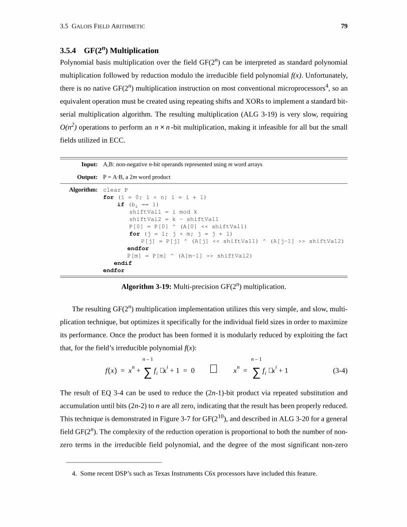
3.5 GALOIS FIELD ARITHMETIC 79
3.5.4 GF(2n) MultiplicationPolynomial basis multiplication over the field GF(2n) can be interpreted as standard polynomial
multiplication followed by reduction modulo the irreducible field polynomial f(x). Unfortunately,
there is no native GF(2n) multiplication instruction on most conventional microprocessors4, so an
equivalent operation must be created using repeating shifts and XORs to implement a standard bit-
serial multiplication algorithm. The resulting multiplication (ALG 3-19) is very slow, requiring
O(n2) operations to perform an -bit multiplication, making it infeasible for all but the small
fields utilized in ECC.
The resulting GF(2n) multiplication implementation utilizes this very simple, and slow, multi-
plication technique, but optimizes it specifically for the individual field sizes in order to maximize
its performance. Once the product has been formed it is modularly reduced by exploiting the fact
that, for the field’s irreducible polynomial f(x):
(3-4)
The result of EQ 3-4 can be used to reduce the (2n-1)-bit product via repeated substitution and
accumulation until bits (2n-2) to n are all zero, indicating that the result has been properly reduced.
This technique is demonstrated in Figure 3-7 for GF(210), and described in ALG 3-20 for a general
field GF(2n). The complexity of the reduction operation is proportional to both the number of non-
zero terms in the irreducible field polynomial, and the degree of the most significant non-zero
4. Some recent DSP’s such as Texas Instruments C6x processors have included this feature.
Input: A,B: non-negative n-bit operands represented using m word arrays
Output: P = A·B, a 2m word product
Algorithm: clear Pfor (i = 0; i < n; i = i + 1)
if (bi == 1)shiftVal1 = i mod kshiftVal2 = k - shiftVal1P[0] = P[0] ^ (A[0] << shiftVal1)for (j = 1; j < m; j = j + 1)
P[j] = P[j] ^ (A[j] << shiftVal1) ^ (A[j-1] >> shiftVal2)endforP[m] = P[m] ^ (A[m-1] >> shiftVal2)
endifendfor
Algorithm 3-19: Multi-precision GF(2n) multiplication.
n n×
f x( ) xn
fi xi
1+⋅
n 1–
∑+ 0 xn⇒ fi x
i1+⋅
n 1–
∑= = =
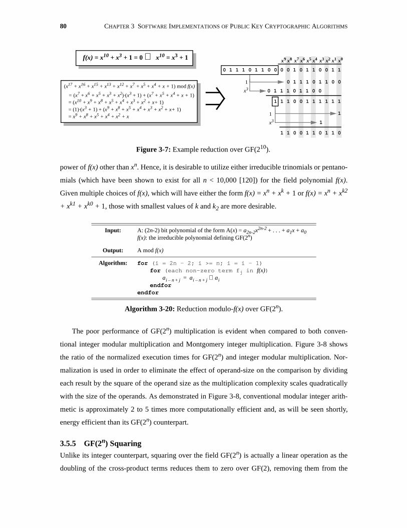
80 CHAPTER 3 SOFTWARE IMPLEMENTATIONS OF PUBLIC KEY CRYPTOGRAPHIC ALGORITHMS
power of f(x) other than xn. Hence, it is desirable to utilize either irreducible trinomials or pentano-
mials (which have been shown to exist for all n < 10,000 [120]) for the field polynomial f(x).
Given multiple choices of f(x), which will have either the form f(x) = xn + xk + 1 or f(x) = xn + xk2
+ xk1 + xk0 + 1, those with smallest values of k and k2 are more desirable.
The poor performance of GF(2n) multiplication is evident when compared to both conven-
tional integer modular multiplication and Montgomery integer multiplication. Figure 3-8 shows
the ratio of the normalized execution times for GF(2n) and integer modular multiplication. Nor-
malization is used in order to eliminate the effect of operand-size on the comparison by dividing
each result by the square of the operand size as the multiplication complexity scales quadratically
with the size of the operands. As demonstrated in Figure 3-8, conventional modular integer arith-
metic is approximately 2 to 5 times more computationally efficient and, as will be seen shortly,
energy efficient than its GF(2n) counterpart.
3.5.5 GF(2n) Squaring
Unlike its integer counterpart, squaring over the field GF(2n) is actually a linear operation as the
doubling of the cross-product terms reduces them to zero over GF(2), removing them from the
Input: A: (2n-2) bit polynomial of the form A(x) = a2n-2x2n-2 + . . . + a1x + a0f(x): the irreducible polynomial defining GF(2n)
Output: A mod f(x)
Algorithm: for (i = 2n - 2; i >= n; i = i - 1)for (each non-zero term fj in f(x))
endforendfor
Algorithm 3-20: Reduction modulo-f(x) over GF(2n).
Figure 3-7: Example reduction over GF(210).
0 1 1 1 0 1 1 0 0 0 0 1 0 1 1 0 0 1 1
f(x) = x10 + x3 + 1 = 0 ⇒ x10 = x3 + 1
0 1 1 1 0 1 1 0 0
0 1 1 1 0 1 1 0 0
1
1 1 1 0 0 1 1 1 1 1 1
1
x3
1
1
x3
1 1 0 0 1 1 0 1 1 0
x8 x7 x6 x5 x4 x3 x2 x1 x0x9
(x17 + x16 + x15 + x13 + x12 + x7 + x5 + x4 + x + 1) mod f(x)
= (x7 + x6 + x5 + x3 + x2)·(x3 + 1) + (x7 + x5 + x4 + x + 1)= (x10 + x9 + x8 + x5 + x4 + x3 + x2 + x+ 1)
= x9 + x8 + x5 + x4 + x2 + x= (1)·(x3 + 1) + (x9 + x8 + x5 + x4 + x3 + x2 + x+ 1)
ai n– j+ ai n– j+ ai⊕=
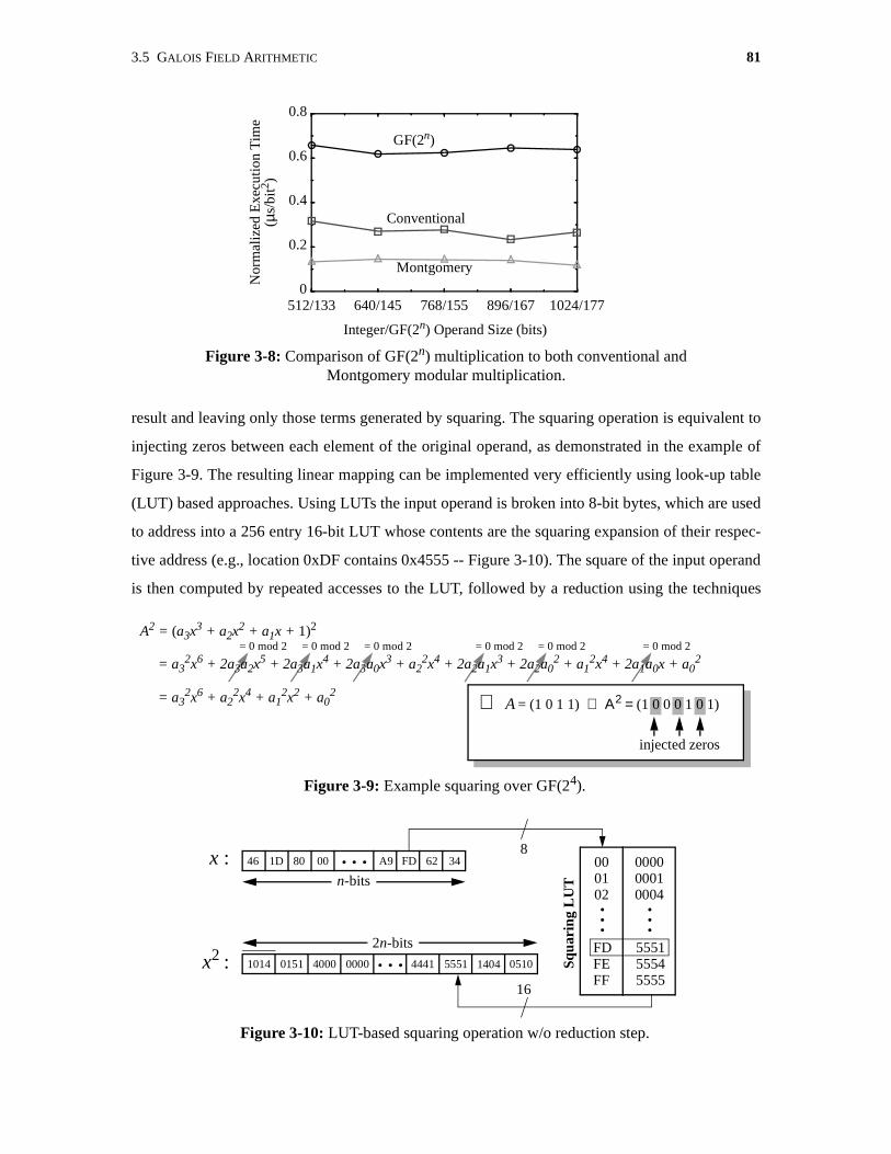
3.5 GALOIS FIELD ARITHMETIC 81
result and leaving only those terms generated by squaring. The squaring operation is equivalent to
injecting zeros between each element of the original operand, as demonstrated in the example of
Figure 3-9. The resulting linear mapping can be implemented very efficiently using look-up table
(LUT) based approaches. Using LUTs the input operand is broken into 8-bit bytes, which are used
to address into a 256 entry 16-bit LUT whose contents are the squaring expansion of their respec-
tive address (e.g., location 0xDF contains 0x4555 -- Figure 3-10). The square of the input operand
is then computed by repeated accesses to the LUT, followed by a reduction using the techniques
Figure 3-8: Comparison of GF(2n) multiplication to both conventional andMontgomery modular multiplication.
Integer/GF(2n) Operand Size (bits)
Nor
mal
ized
Exe
cuti
on T
ime
(µs/
bit2 )
512/133 640/145 768/155 896/167 1024/1770
0.2
0.4
0.6
0.8
Montgomery
Conventional
GF(2n)
= 0 mod 2= 0 mod 2= 0 mod 2= 0 mod 2= 0 mod 2= 0 mod 2
Figure 3-9: Example squaring over GF(24).
A2 = (a3x3 + a2x2 + a1x + 1)2
= a32x6 + 2a3a2x5 + 2a3a1x4 + 2a3a0x3 + a2
2x4 + 2a2a1x3 + 2a2a02 + a1
2x4 + 2a1a0x + a02
= a32x6 + a2
2x4 + a12x2 + a0
2= (1 0 1 1) ⇒ Α 2 = (1 0 0 0 1 0 1)
injected zeros
A∴
Figure 3-10: LUT-based squaring operation w/o reduction step.
. . .n-bits
. . .
x :
x2 :
000000010004
555155545555
. . .
000102
FDFEFF
8FD 3462A98046 1D 00
. . .2n-bits
5551 05101404444140001014 0151 0000
16
Squa
ring
LU
T
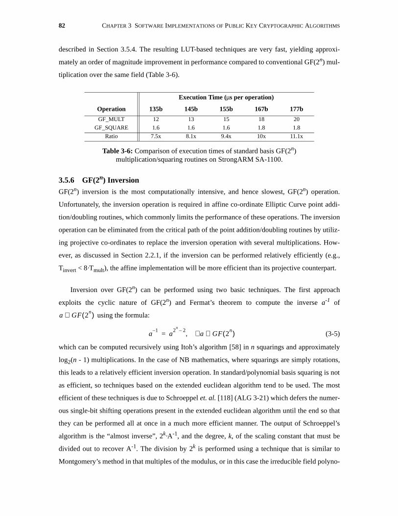
82 CHAPTER 3 SOFTWARE IMPLEMENTATIONS OF PUBLIC KEY CRYPTOGRAPHIC ALGORITHMS
described in Section 3.5.4. The resulting LUT-based techniques are very fast, yielding approxi-
mately an order of magnitude improvement in performance compared to conventional GF(2n) mul-
tiplication over the same field (Table 3-6).
3.5.6 GF(2n) Inversion
GF(2n) inversion is the most computationally intensive, and hence slowest, GF(2n) operation.
Unfortunately, the inversion operation is required in affine co-ordinate Elliptic Curve point addi-
tion/doubling routines, which commonly limits the performance of these operations. The inversion
operation can be eliminated from the critical path of the point addition/doubling routines by utiliz-
ing projective co-ordinates to replace the inversion operation with several multiplications. How-
ever, as discussed in Section 2.2.1, if the inversion can be performed relatively efficiently (e.g.,
Tinvert < 8·Tmult), the affine implementation will be more efficient than its projective counterpart.
Inversion over GF(2n) can be performed using two basic techniques. The first approach
exploits the cyclic nature of GF(2n) and Fermat’s theorem to compute the inverse a-1 of
using the formula:
(3-5)
which can be computed recursively using Itoh’s algorithm [58] in n squarings and approximately
log2(n - 1) multiplications. In the case of NB mathematics, where squarings are simply rotations,
this leads to a relatively efficient inversion operation. In standard/polynomial basis squaring is not
as efficient, so techniques based on the extended euclidean algorithm tend to be used. The most
efficient of these techniques is due to Schroeppel et. al. [118] (ALG 3-21) which defers the numer-
ous single-bit shifting operations present in the extended euclidean algorithm until the end so that
they can be performed all at once in a much more efficient manner. The output of Schroeppel’s
algorithm is the “almost inverse”, 2k·A-1, and the degree, k, of the scaling constant that must be
divided out to recover A-1. The division by 2k is performed using a technique that is similar to
Montgomery’s method in that multiples of the modulus, or in this case the irreducible field polyno-
Execution Time (µs per operation)
Operation 135b 145b 155b 167b 177b
GF_MULT 12 13 15 18 20
GF_SQUARE 1.6 1.6 1.6 1.8 1.8
Ratio 7.5x 8.1x 9.4x 10x 11.1x
Table 3-6: Comparison of execution times of standard basis GF(2n)multiplication/squaring routines on StrongARM SA-1100.
a GF 2n( )∈
a1–
a2
n2–
a GF 2n( )∈∀,=
3.5 GALOIS FIELD ARITHMETIC 83
mial f(x), are added to the result in order to zero out the least significant k bits so that shifting
doesn’t destroy information and corrupt the result.
The resulting GF(2n) inversion performance on the StrongARM SA-1100 (Table 3-7) is quite
good, with execution times of approximately 6·Tmult, leading to very efficient elliptic curve point
operations, that don’t require the additional overhead and complexity of a projective implementa-
tion.
Execution Time (µs per operation)
Operation 135b 145b 155b 167b 177b
GF_MULT 12 13 15 18 20
GF_INVERT 75 85 83 118 123
Ratio 6.3x 6.5x 5.5x 6.6x 6.2x
Table 3-7: Execution times of GF(2n) multiplication and inversion routines onStrongARM SA-1100.
Input: A: binary vector representing element of GF(2n) that is to be invertedf(x): the irreducible polynomial defining GF(2n)
Output: B = 2k·A-1: element of GF(2n) that is the inverse of Ak: degree of scaling constant that must be removed
Algorithm:
loop:
B = 1C = 0F = AG = f(x)while (F0 = 0)
F = F/2C = 2·Ck = k + 1
endwhileif (F == 1)
return(B,k)endifif (degree(F) < degree(G))
temp = F;F = G;G = temp;temp = B;B = C;C = temp;
endifF = F + GB = B + Cgoto loop:
// F0 = LSB of F
// exit routine
// swap F, G
// swap B, C
Algorithm 3-21: Schroeppel’s almost inverse algorithm.
84 CHAPTER 3 SOFTWARE IMPLEMENTATIONS OF PUBLIC KEY CRYPTOGRAPHIC ALGORITHMS
3.5.7 GF(2n) ExponentiationGF(2n) exponentiation is the equivalent of modular exponentiation and all of the aforementioned
techniques from Section 3.4.7 can be utilized directly, including Montgomery’s techniques [70].
However, due to the lack of a native multiplication instruction, the poor perfor-
mance of GF(2n) multiplication makes exponentiation all but unusable compared to an equivalent
modular exponentiation operation. Hence, GF(2n) exponentiation is not included as part of the
GF(2n) arithmetic package developed in this dissertation.
3.6 Elliptic Curve ArithmeticAs described in Section 2.2, elliptic curve arithmetic is performed utilizing operations defined over
the field upon which the curve is constructed, which for the purposes of this dissertation is GF(2n).
Hence, the elliptic curve operations rely on the various GF(2n) operations described in Section 3.5.
The following two subsections describe the implementation of the fundamental elliptic curve
operations of point addition, point doubling, and point multiplication. Additional, auxiliary func-
tions such as point and curve generation are also implemented using the resulting elliptic curve
arithmetic functions and the algorithms provided in IEEE P1363, but not described here. The
reader is referred to [56] for further information regarding these auxiliary functions.
3.6.1 Point Addition and DoublingThe group operation for the points of an elliptic curve is addition. If two distinct points are to be
added then the addition formulae of Section 2.2.3 can be used to perform the required operation,
and if they are not then the corresponding doubling formulae can be used instead. In both cases the
formulae for curves of characteristic 2 (EQ 2-27 and EQ 2-28) should be used as the curves con-
sidered in this dissertation are constructed over GF(2n). The resulting point addition algorithm is
given by ALG 3-22, and its corresponding point doubling counterpart is described in ALG 3-23.
3.6.2 Point Multiplication
The basic cryptographic primitive in Elliptic Curve Cryptography is point multiplication, which is
the additive group analog of a multiplicative group’s (e.g., ZN*) modular exponentiation operation.
Thus, elliptic curve point multiplication can be performed using the additive analogs of any of the
exponentiation techniques of Section 3.4.7. In order to convert the exponentiation techniques to
their additive equivalent, one simply replaces the squaring operations with point doublings, and
multiplications with point additions. Applying this transformation to the simple binary method of
ALG 3-14 yields the binary point multiplication method of ALG 3-24, which will require on aver-
GF 2w( ) GF 2
w( )×

3.6 ELLIPTIC CURVE ARITHMETIC 85
age n/2 point additions, and n point doublings.
Input: P1 = (x1, y1), P2 = (x2, y2): curve points on elliptic curve E that are to be added togethera = curve parameter that defines the elliptic curve E over the base field GF(2n)
Output: P3 = P1 + P2 = (x3, y3)
Algorithm: if (P1 == point at infinity)P3 = P2
elseif (P2 == point at infinity)P3 = P1
elseif (x1 == x2)P3 = EC_DOUBLE(P1)
elset1 = GF_ADD(x1,x2)t2 = GF_ADD(y1,y2)λ = GF_INV(t2)λ = GF_MULT(λ,t1)t2 = GF_SQUARE(λ)t2 = GF_ADD(t2,λ)t2 = GF_ADD(t2,t1)t2 = GF_ADD(t2,a)t1 = GF_ADD(t1,x2)t1 = GF_MULT(λ,t1)t1 = GF_ADD(t1,t2)y3 = GF_ADD(t1,y2)x3 = t2
endif
// check if P1 is valid
// check if P2 is valid
// check if P1 = P2// if so, double it
// t1 = x1 + x2// t2 = y1 + y2// λ = 1/(y1 + y2)// λ = (x1 + x2)/(y1 + y2)// t2 = λ2// t2 = λ2 + λ// t2 = λ2 + λ + x1 + x2// t2 = x3 = λ2 + λ + x1 + x2 + a// t1 = x3 + x2// t1 = λ(x3 + x2)// t1 = λ(x3 + x2) + x3// y3 = λ(x3 + x2) + x3 + y2// x3 = λ2 + λ + x1 + x2 + a
Algorithm 3-22: EC point addition operation.
Input: P1 = (x1, y1): curve point on elliptic curve E that is to be doubleda = curve parameter that defines the elliptic curve E over the base field GF(2n)
Output: P3 = 2·P1 = (x3, y3)
Algorithm: if (P1 == point at infinity)P3 = P2
elseλ = GF_INV(x1)λ = GF_MULT(λ,y1)λ = GF_ADD(λ,x1)t2 = GF_SQUARE(λ)t2 = GF_ADD(t2,λ)t2 = GF_ADD(t2,a)t1 = GF_ADD(t2,x1)t1 = GF_MULT(λ,t1)t1 = GF_ADD(t1,t2)y3 = GF_ADD(t1,y1)x3 = t2
endif
// check if P1 is valid
// λ = 1/x1// λ = y1/x1 // λ = x1 + y1/x1 // t2 = λ2// t2 = λ2 + λ// t2 = x3 = λ2 + λ + a// t1 = x3 + x1// t1 = λ(x3 + x1)// t1 = λ(x3 + x1) + x3// y3 = λ(x3 + x1) + x3 + y1// x3 = λ2 + λ + a
Algorithm 3-23: EC point doubling operation.
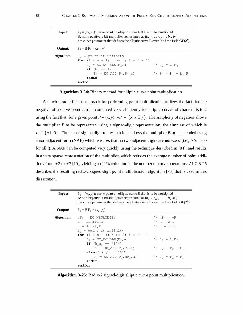
86 CHAPTER 3 SOFTWARE IMPLEMENTATIONS OF PUBLIC KEY CRYPTOGRAPHIC ALGORITHMS
A much more efficient approach for performing point multiplication utilizes the fact that the
negative of a curve point can be computed very efficiently for elliptic curves of characteristic 2
using the fact that, for a given point P = (x, y), . The simplicity of negation allows
the multiplier E to be represented using a signed-digit representation, the simplest of which is
. The use of signed digit representations allows the multiplier B to be encoded using
a non-adjacent form (NAF) which ensures that no two adjacent digits are non-zero (i.e., bibi-1 = 0
for all i). A NAF can be computed very quickly using the technique described in [84], and results
in a very sparse representation of the multiplier, which reduces the average number of point addi-
tions from n/2 to n/3 [10], yielding an 11% reduction in the number of curve operations. ALG 3-25
describes the resulting radix-2 signed-digit point multiplication algorithm [73] that is used in this
dissertation.
Input: P1 = (x1, y1): curve point on elliptic curve E that is to be multipliedB: non-negative n-bit multiplier represented as (bn-1, bn-2, . . . , b1, b0)a = curve parameter that defines the elliptic curve E over the base field GF(2n)
Output: P2 = B·P1 = (x2, y2)
Algorithm: P2 = point at infinityfor (i = n - 1; i >= 0; i = i - 1)
P2 = EC_DOUBLE(P2,a)if (bi == 1)
P2 = EC_ADD(P2,P1,a)endif
endfor
// P2 = 2·P2
// P2 = P2 + bi·P1
Algorithm 3-24: Binary method for elliptic curve point multiplication.
Input: P1 = (x1, y1): curve point on elliptic curve E that is to be multipliedB: non-negative n-bit multiplier represented as (bn-1, bn-2, . . . , b1, b0)a = curve parameter that defines the elliptic curve E over the base field GF(2n)
Output: P2 = B·P1 = (x2, y2)
Algorithm: nP1 = EC_NEGATE(P1)H = LSHIFT(B)H = ADD(H,B)P2 = point at infinityfor (i = n - 1; i >= 0; i = i - 1)
P2 = EC_DOUBLE(P2,a)if (hibi == “10”)
P2 = EC_ADD(P2,P1,a)elseif (hibi = “01”)
P2 = EC_ADD(P2,nP1,a)endif
endfor
// nP1 = -P1// H = 2·B// H = 3·B
// P2 = 2·P2
// P2 = P2 + P1
// P2 = P2 - P1
Algorithm 3-25: Radix-2 signed-digit elliptic curve point multiplication.
P– x x y⊕,( )=
bi 1 0,±{ }∈

3.7 ENERGY EFFICIENCY OF SOFTWARE-BASED ASYMMETRIC CRYPTOGRAPHY 87
3.7 Energy Efficiency of Software-based Asymmetric CryptographyThe performance and energy consumption of the multi-precision modular integer arithmetic pack-
age are summarized in Table 3-8 and Table 3-9 respectively, for a variety of operand sizes. The
corresponding data for the field-specific GF(2n) operations, and resulting elliptic curve operations
are summarized in Table 3-10 and Table 3-11.
Execution Time (s per operation)
Operation 512b 640b 768b 896b 1024b
MOD 60µ 80µ 115µ 133µ 167µMOD_MULT 83µ 111µ 163µ 187µ 280µMOD_SQUARE 74µ 101µ 125µ 165µ 235µMOD_EXP 55.4m 96.2m 147.0m 221.6m 300.6m
MONT_MULT 34.8µ 59.4µ 83.8µ 112.0µ 132.8µMONT_SQUARE 33.0µ 48.0µ 66.4µ 88.4µ 112.6µ
MONT_EXP (k = 5) 22.3m 40.5m 66.5m 102.7m 149.8m
Table 3-8: Execution times of modular arithmetic routines on SA-1100.
Energy Consumption (J per operation)
Operation 512b 640b 768b 896b 1024b
MOD 19.4µ 26µ 37.4µ 43.5µ 54.9µMOD_MULT 27.2µ 36.5µ 53.9µ 61.9µ 93.1µMOD_SQUARE 24.3µ 33.3µ 41.3µ 54.6µ 76.9µMOD_EXP 18.0m 31.4m 48.4m 73.1m 99.8m
MONT_MULT 11.9µ 20.4µ 28.7µ 38.4µ 42.1µMONT_SQUARE 11.3µ 16.5µ 22.8µ 30.4µ 38.6µ
MONT_EXP (k = 5) 7.6m 13.9m 22.8m 35.2m 51.5m
Table 3-9: Energy consumption of modular arithmetic routines on SA-1100.
Execution Time (s per operation)
Operation 135b 145b 155b 167b 177b
GF_REDUCE 0.45µ 0.51µ 0.51µ 0.52µ 0.56µGF_MULT 12µ 13µ 15µ 18µ 20µGF_SQUARE 1.6µ 1.6µ 1.6µ 1.8µ 1.8µGF_INVERT 75µ 85µ 83µ 118µ 123µEC_ADD 106.2µ 115.5µ 123.0µ 154.8µ 163.3µ
EC_DOUBLE 106.1µ 114.8µ 121.4µ 152.0µ 164.3µEC_MULT 19.0m 22.0m 25.4m 34.3m 38.8m
Table 3-10: Execution times of standard basis GF(2n) routines on SA-1100.

88 CHAPTER 3 SOFTWARE IMPLEMENTATIONS OF PUBLIC KEY CRYPTOGRAPHIC ALGORITHMS
The energy inefficiency of asymmetric cryptographic algorithms is evident when one com-
pares the energy efficiencies of Table 3-9 and 3-11 to that of symmetric algorithms. The energy
efficiency of the RC6 encryption algorithm was computed using an optimized assembly language
implementation on the StrongARM-SA1100 which achieved an encryption/decryption rate of 197/
213 Mb/s for an energy efficiency of 1.8/1.7 nJ/bit. In comparison, asymmetric cryptographic
primitives such as RSA, Diffie-Hellman, and Elliptic Curve techniques with a corresponding level
of security (i.e., 1024-bit modular exponentiation and 177-bit elliptic curve point multiplication)
require either 13.7 mJ/op or 51.5 mJ/op. Hence, the energy required for a single asymmetric oper-
ation is equivalent to the amount of energy it would take to encrypt either 7.6 Mb or 28.6 Mb using
a symmetric algorithm. In the case of portable applications such as web-based transactions where
the amount of data being transferred is typically quite small, and the user is required to perform
fairly frequent asymmetric operations for establishing new secure connections and performing
data/user authentication, it is quite likely that energy consumption of the asymmetric operations
will represent a significant percentage of total energy consumption required for utilizing cryptog-
raphy. In Chapter 5 this energy consumption issue is addressed through the use of flexible hard-
ware that is several orders of magnitude more energy efficient than the software-based solutions
described here.
3.7.1 Comparison of IF, DL, and EC-based Software Energy EfficienciesThe performance and energy efficiency of the IF, DL, and EC-based schemes can be compared
using the fact that modular exponentiation in the IF and DL based schemes is the analog of point
multiplication in the EC-based scheme. The operand sizes differ significantly however because of
the fact that the best known attacks on EC based schemes are exponential-time algorithms, while
those for IF and DL based schemes are subexponential. However, the operand sizes can be equated
by deriving a relation between nEC and nIF/DL (i.e., bit lengths of their respective operands) based
Energy Consumption (J per operation)
Operation 135b 145b 155b 167b 177b
GF_REDUCT 0.16µ 0.18µ 0.18µ 0.18µ 0.20µGF_MULT 4.23µ 4.58µ 5.29µ 6.35µ 7.05µGF_SQUARE 0.55µ 0.57µ 0.57µ 0.63µ 0.64µGF_INVERT 26.44µ 29.96µ 29.26µ 41.60µ 43.36µEC_ADD 37.44µ 40.71µ 43.36µ 54.57µ 57.56µ
EC_DOUBLE 37.40µ 40.47µ 42.79µ 53.58µ 57.92µEC_MULT 6.70m 7.76m 8.95m 12.09m 13.68m
Table 3-11: Energy consumption of standard basis GF(2n) routines on SA-1100.
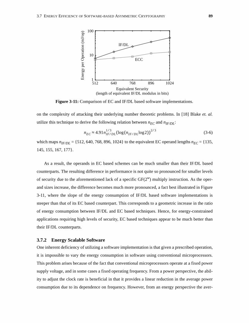
3.7 ENERGY EFFICIENCY OF SOFTWARE-BASED ASYMMETRIC CRYPTOGRAPHY 89
on the complexity of attacking their underlying number theoretic problems. In [18] Blake et. al.
utilize this technique to derive the following relation between nEC and nIF/DL:
(3-6)
which maps nIF/DL = {512, 640, 768, 896, 1024} to the equivalent EC operand lengths nEC = {135,
145, 155, 167, 177}.
As a result, the operands in EC based schemes can be much smaller than their IF/DL based
counterparts. The resulting difference in performance is not quite so pronounced for smaller levels
of security due to the aforementioned lack of a specific GF(2w) multiply instruction. As the oper-
and sizes increase, the difference becomes much more pronounced, a fact best illustrated in Figure
3-11, where the slope of the energy consumption of IF/DL based software implementations is
steeper than that of its EC based counterpart. This corresponds to a geometric increase in the ratio
of energy consumption between IF/DL and EC based techniques. Hence, for energy-constrained
applications requiring high levels of security, EC based techniques appear to be much better than
their IF/DL counterparts.
3.7.2 Energy Scalable Software
One inherent deficiency of utilizing a software implementation is that given a prescribed operation,
it is impossible to vary the energy consumption in software using conventional microprocessors.
This problem arises because of the fact that conventional microprocessors operate at a fixed power
supply voltage, and in some cases a fixed operating frequency. From a power perspective, the abil-
ity to adjust the clock rate is beneficial in that it provides a linear reduction in the average power
consumption due to its dependence on frequency. However, from an energy perspective the aver-
nEC 4.91nIF DL⁄1 3⁄
nIF DL⁄ 2log( )log( )2 3⁄≈
Figure 3-11: Comparison of EC and IF/DL based software implementations.
512 640 768 896 10241
10
100
ECC
IF/DL
Equivalent Security
Ene
rgy
per
Ope
ratio
n (m
J/op
)
(length of equivalent IF/DL modulus in bits)

90 CHAPTER 3 SOFTWARE IMPLEMENTATIONS OF PUBLIC KEY CRYPTOGRAPHIC ALGORITHMS
age energy consumption doesn’t change because energy is independent of operating frequency as
you operate at half the power but take twice as long so the energy remains constant:
(3-7)
Thus, a given operation will consume the same amount of energy, regardless of the throughput
of the processor. In practical terms this means that regardless of whether you are encrypting at 106
bps or 10 bps, each of those bits will consume the same amount of energy. In fact, at low rates the
energy consumption will actually increase as power is dissipated even during periods of inactivity
due to leakage currents within the processor. Hence, the simple averaging used in EQ 3-7 will
yield an overly conservative estimate of the energy consumption.
Ehalf rate–12---P
2t( ) Pt Efull rate–= = =
Figure 3-12: Minimum supply voltage vs. clock frequency of the StrongARM SA-1100.
50 100 150 200 250Operating Frequency (MHz)
1.4
1.2
1.0
0.8
0.6M
inim
um V
DD
(V
)
Figure 3-13: Average energy consumption per cycle of operation of the StrongARMSA-1100 as a function of the clock frequency and supply voltage
1.61.5
1.41.3
1.21.1
1.00.9
206.4176.9
147.5118.0
88.5 59.0
0
0.2
0.4
0.6
0.8
1
Core Voltage (V)Frequency (MHz)
Ene
rgy
per
Inst
ruct
ion
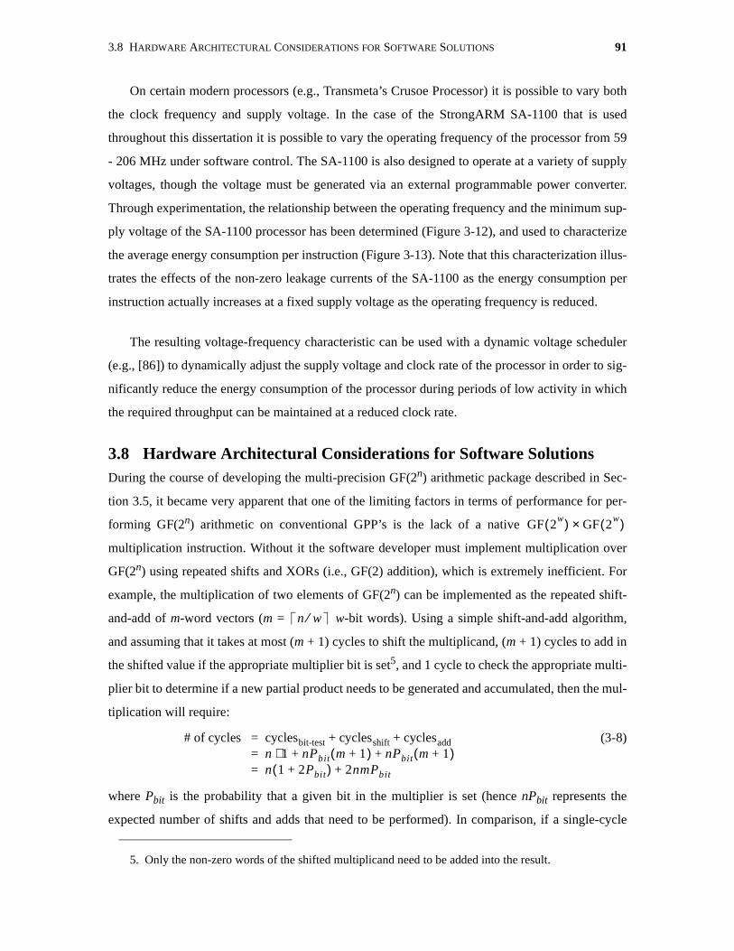
3.8 HARDWARE ARCHITECTURAL CONSIDERATIONS FOR SOFTWARE SOLUTIONS 91
On certain modern processors (e.g., Transmeta’s Crusoe Processor) it is possible to vary both
the clock frequency and supply voltage. In the case of the StrongARM SA-1100 that is used
throughout this dissertation it is possible to vary the operating frequency of the processor from 59
- 206 MHz under software control. The SA-1100 is also designed to operate at a variety of supply
voltages, though the voltage must be generated via an external programmable power converter.
Through experimentation, the relationship between the operating frequency and the minimum sup-
ply voltage of the SA-1100 processor has been determined (Figure 3-12), and used to characterize
the average energy consumption per instruction (Figure 3-13). Note that this characterization illus-
trates the effects of the non-zero leakage currents of the SA-1100 as the energy consumption per
instruction actually increases at a fixed supply voltage as the operating frequency is reduced.
The resulting voltage-frequency characteristic can be used with a dynamic voltage scheduler
(e.g., [86]) to dynamically adjust the supply voltage and clock rate of the processor in order to sig-
nificantly reduce the energy consumption of the processor during periods of low activity in which
the required throughput can be maintained at a reduced clock rate.
3.8 Hardware Architectural Considerations for Software SolutionsDuring the course of developing the multi-precision GF(2n) arithmetic package described in Sec-
tion 3.5, it became very apparent that one of the limiting factors in terms of performance for per-
forming GF(2n) arithmetic on conventional GPP’s is the lack of a native
multiplication instruction. Without it the software developer must implement multiplication over
GF(2n) using repeated shifts and XORs (i.e., GF(2) addition), which is extremely inefficient. For
example, the multiplication of two elements of GF(2n) can be implemented as the repeated shift-
and-add of m-word vectors (m = w-bit words). Using a simple shift-and-add algorithm,
and assuming that it takes at most (m + 1) cycles to shift the multiplicand, (m + 1) cycles to add in
the shifted value if the appropriate multiplier bit is set5, and 1 cycle to check the appropriate multi-
plier bit to determine if a new partial product needs to be generated and accumulated, then the mul-
tiplication will require:
(3-8)
where Pbit is the probability that a given bit in the multiplier is set (hence nPbit represents the
expected number of shifts and adds that need to be performed). In comparison, if a single-cycle
5. Only the non-zero words of the shifted multiplicand need to be added into the result.
GF 2w( ) GF 2w( )×
n w⁄
# of cycles cyclesbit-test cyclesshift cyclesadd+ +n 1 nPbit m 1+( ) nPbit m 1+( )+ +⋅n 1 2Pbit+( ) 2nmPbit+
===
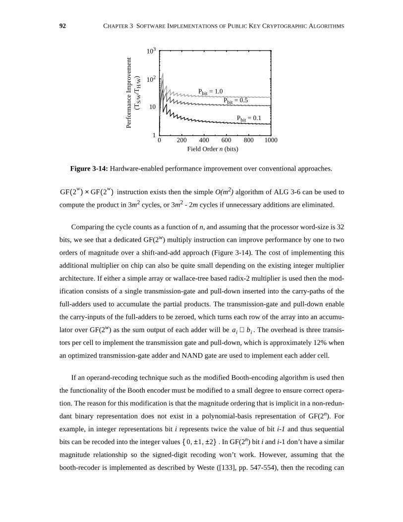
92 CHAPTER 3 SOFTWARE IMPLEMENTATIONS OF PUBLIC KEY CRYPTOGRAPHIC ALGORITHMS
instruction exists then the simple O(m2) algorithm of ALG 3-6 can be used to
compute the product in 3m2 cycles, or 3m2 - 2m cycles if unnecessary additions are eliminated.
Comparing the cycle counts as a function of n, and assuming that the processor word-size is 32
bits, we see that a dedicated GF(2w) multiply instruction can improve performance by one to two
orders of magnitude over a shift-and-add approach (Figure 3-14). The cost of implementing this
additional multiplier on chip can also be quite small depending on the existing integer multiplier
architecture. If either a simple array or wallace-tree based radix-2 multiplier is used then the mod-
ification consists of a single transmission-gate and pull-down inserted into the carry-paths of the
full-adders used to accumulate the partial products. The transmission-gate and pull-down enable
the carry-inputs of the full-adders to be zeroed, which turns each row of the array into an accumu-
lator over GF(2w) as the sum output of each adder will be . The overhead is three transis-
tors per cell to implement the transmission gate and pull-down, which is approximately 12% when
an optimized transmission-gate adder and NAND gate are used to implement each adder cell.
If an operand-recoding technique such as the modified Booth-encoding algorithm is used then
the functionality of the Booth encoder must be modified to a small degree to ensure correct opera-
tion. The reason for this modification is that the magnitude ordering that is implicit in a non-redun-
dant binary representation does not exist in a polynomial-basis representation of GF(2n). For
example, in integer representations bit i represents twice the value of bit i-1 and thus sequential
bits can be recoded into the integer values . In GF(2n) bit i and i-1 don’t have a similar
magnitude relationship so the signed-digit recoding won’t work. However, assuming that the
booth-recoder is implemented as described by Weste ([133], pp. 547-554), then the recoding can
GF 2w( ) GF 2
w( )×
ai bi⊕
Figure 3-14: Hardware-enabled performance improvement over conventional approaches.
Field Order n (bits)
Perf
orm
ance
Im
prov
emen
t
0 200 400 600 800 10001
10
102
103
(TS
/W/T
H/W
)
Pbit = 1.0Pbit = 0.5
Pbit = 0.1
0 1 2±,±,{ }
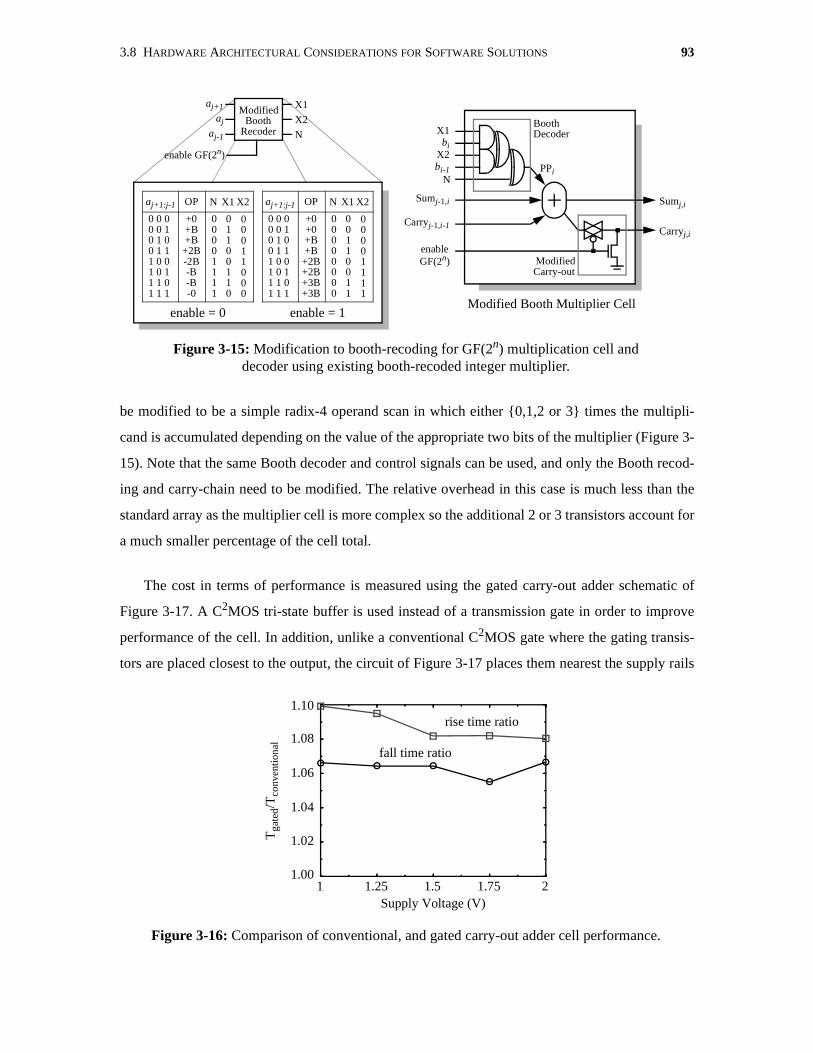
3.8 HARDWARE ARCHITECTURAL CONSIDERATIONS FOR SOFTWARE SOLUTIONS 93
be modified to be a simple radix-4 operand scan in which either {0,1,2 or 3} times the multipli-
cand is accumulated depending on the value of the appropriate two bits of the multiplier (Figure 3-
15). Note that the same Booth decoder and control signals can be used, and only the Booth recod-
ing and carry-chain need to be modified. The relative overhead in this case is much less than the
standard array as the multiplier cell is more complex so the additional 2 or 3 transistors account for
a much smaller percentage of the cell total.
The cost in terms of performance is measured using the gated carry-out adder schematic of
Figure 3-17. A C2MOS tri-state buffer is used instead of a transmission gate in order to improve
performance of the cell. In addition, unlike a conventional C2MOS gate where the gating transis-
tors are placed closest to the output, the circuit of Figure 3-17 places them nearest the supply rails
Figure 3-15: Modification to booth-recoding for GF(2n) multiplication cell anddecoder using existing booth-recoded integer multiplier.
X1
X2bi
bi-1N
PPi
aj
aj-1
aj+1
X2
N
X1ModifiedBooth
Recoder
Sumj-1,i
Carryj-1,i-1
enable
Sumj,i
Carryj,i
aj+1:j-1
0 0 00 0 10 1 00 1 11 0 01 0 11 1 01 1 1
OP
+0+0+B+B
+2B+2B+3B+3B
N
00000000
X1
00110011
00001111
X2
GF(2n)
enable GF(2n)
enable = 0 enable = 1
aj+1:j-1
0 0 00 0 10 1 00 1 11 0 01 0 11 1 01 1 1
OP
+0+B+B
+2B-2B-B-B-0
N
00001111
X1
01100110
00011000
X2
Modified Booth Multiplier Cell
BoothDecoder
ModifiedCarry-out
Figure 3-16: Comparison of conventional, and gated carry-out adder cell performance.
1 1.25 1.5 1.75 21.00
1.02
1.04
1.06
1.08
1.10
Supply Voltage (V)
Tga
ted/
Tco
nven
tion
al
fall time ratio
rise time ratio
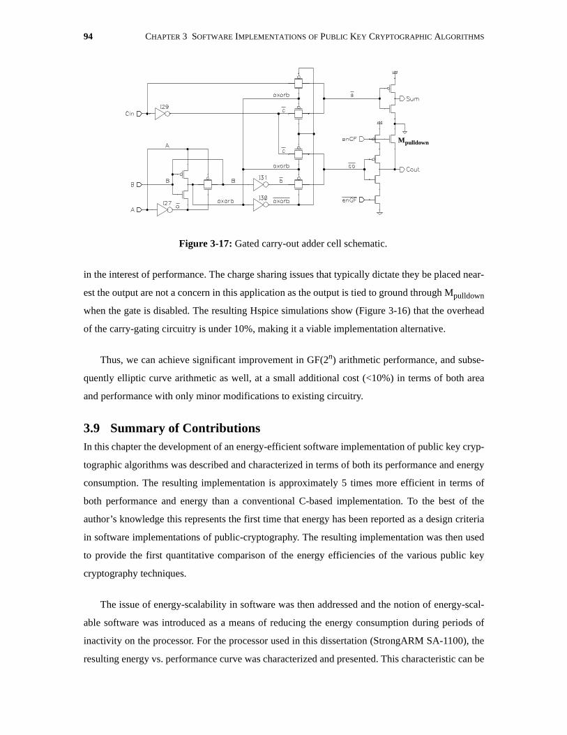
94 CHAPTER 3 SOFTWARE IMPLEMENTATIONS OF PUBLIC KEY CRYPTOGRAPHIC ALGORITHMS
in the interest of performance. The charge sharing issues that typically dictate they be placed near-
est the output are not a concern in this application as the output is tied to ground through Mpulldown
when the gate is disabled. The resulting Hspice simulations show (Figure 3-16) that the overhead
of the carry-gating circuitry is under 10%, making it a viable implementation alternative.
Thus, we can achieve significant improvement in GF(2n) arithmetic performance, and subse-
quently elliptic curve arithmetic as well, at a small additional cost (<10%) in terms of both area
and performance with only minor modifications to existing circuitry.
3.9 Summary of ContributionsIn this chapter the development of an energy-efficient software implementation of public key cryp-
tographic algorithms was described and characterized in terms of both its performance and energy
consumption. The resulting implementation is approximately 5 times more efficient in terms of
both performance and energy than a conventional C-based implementation. To the best of the
author’s knowledge this represents the first time that energy has been reported as a design criteria
in software implementations of public-cryptography. The resulting implementation was then used
to provide the first quantitative comparison of the energy efficiencies of the various public key
cryptography techniques.
The issue of energy-scalability in software was then addressed and the notion of energy-scal-
able software was introduced as a means of reducing the energy consumption during periods of
inactivity on the processor. For the processor used in this dissertation (StrongARM SA-1100), the
resulting energy vs. performance curve was characterized and presented. This characteristic can be
Figure 3-17: Gated carry-out adder cell schematic.
Mpulldown

3.9 SUMMARY OF CONTRIBUTIONS 95
used in conjunction with a dynamic voltage scheduler to yield a full energy-scalable software
implementation.
The chapter closed with the description of a relatively simple architectural modification to the
processor’s integer multiplier that can increase the performance of GF(2n)-based algorithms in
software by approximately an order of magnitude. The modification requires only a small amount
of overhead (<10%) in terms of both performance and area, making it a viable implementation
alternative for future processors.

96 CHAPTER 3 SOFTWARE IMPLEMENTATIONS OF PUBLIC KEY CRYPTOGRAPHIC ALGORITHMS
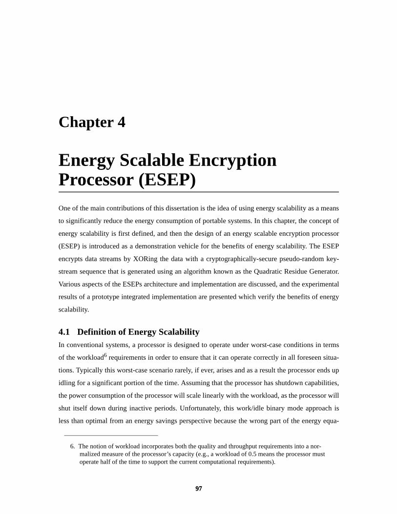
979797
Chapter 4
Energy Scalable Encryption Processor (ESEP)One of the main contributions of this dissertation is the idea of using energy scalability as a means
to significantly reduce the energy consumption of portable systems. In this chapter, the concept of
energy scalability is first defined, and then the design of an energy scalable encryption processor
(ESEP) is introduced as a demonstration vehicle for the benefits of energy scalability. The ESEP
encrypts data streams by XORing the data with a cryptographically-secure pseudo-random key-
stream sequence that is generated using an algorithm known as the Quadratic Residue Generator.
Various aspects of the ESEPs architecture and implementation are discussed, and the experimental
results of a prototype integrated implementation are presented which verify the benefits of energy
scalability.
4.1 Definition of Energy ScalabilityIn conventional systems, a processor is designed to operate under worst-case conditions in terms
of the workload6 requirements in order to ensure that it can operate correctly in all foreseen situa-
tions. Typically this worst-case scenario rarely, if ever, arises and as a result the processor ends up
idling for a significant portion of the time. Assuming that the processor has shutdown capabilities,
the power consumption of the processor will scale linearly with the workload, as the processor will
shut itself down during inactive periods. Unfortunately, this work/idle binary mode approach is
less than optimal from an energy savings perspective because the wrong part of the energy equa-
6. The notion of workload incorporates both the quality and throughput requirements into a nor-malized measure of the processor’s capacity (e.g., a workload of 0.5 means the processor must operate half of the time to support the current computational requirements).
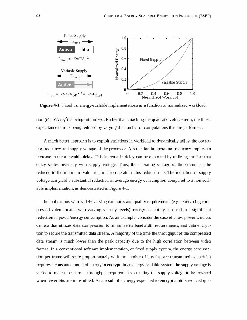
98 CHAPTER 4 ENERGY SCALABLE ENCRYPTION PROCESSOR (ESEP)
tion (E = CVDD2) is being minimized. Rather than attacking the quadratic voltage term, the linear
capacitance term is being reduced by varying the number of computations that are performed.
A much better approach is to exploit variations in workload to dynamically adjust the operat-
ing frequency and supply voltage of the processor. A reduction in operating frequency implies an
increase in the allowable delay. This increase in delay can be exploited by utilizing the fact that
delay scales inversely with supply voltage. Thus, the operating voltage of the circuit can be
reduced to the minimum value required to operate at this reduced rate. The reduction in supply
voltage can yield a substantial reduction in average energy consumption compared to a non-scal-
able implementation, as demonstrated in Figure 4-1.
In applications with widely varying data rates and quality requirements (e.g., encrypting com-
pressed video streams with varying security levels), energy scalability can lead to a significant
reduction in power/energy consumption. As an example, consider the case of a low power wireless
camera that utilizes data compression to minimize its bandwidth requirements, and data encryp-
tion to secure the transmitted data stream. A majority of the time the throughput of the compressed
data stream is much lower than the peak capacity due to the high correlation between video
frames. In a conventional software implementation, or fixed supply system, the energy consump-
tion per frame will scale proportionately with the number of bits that are transmitted as each bit
requires a constant amount of energy to encrypt. In an energy-scalable system the supply voltage is
varied to match the current throughput requirements, enabling the supply voltage to be lowered
when fewer bits are transmitted. As a result, the energy expended to encrypt a bit is reduced qua-
Figure 4-1: Fixed vs. energy-scalable implementations as a function of normalized workload.
0 0.2 0.4 0.6 0.8 1.00
0.2
0.4
0.6
0.8
1.0
Normalized Workload
Nor
mal
ized
Ene
rgy
Fixed Supply
Variable Supply
Active Idle
Efixed = 1/2•CVdd2
Tframe
Fixed Supply
Tframe
Active
Variable Supply
Evar = 1/2•C(Vdd/2)2 = 1/4•Efixed
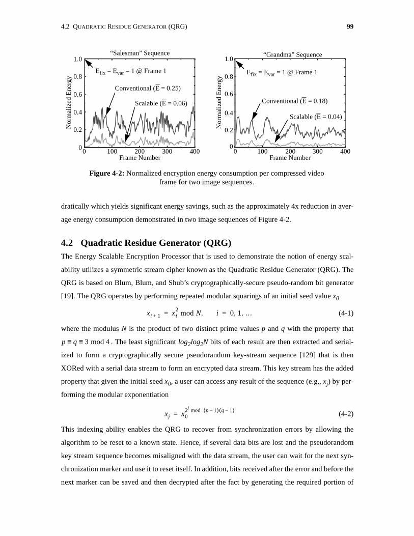
4.2 QUADRATIC RESIDUE GENERATOR (QRG) 99
dratically which yields significant energy savings, such as the approximately 4x reduction in aver-
age energy consumption demonstrated in two image sequences of Figure 4-2.
4.2 Quadratic Residue Generator (QRG)The Energy Scalable Encryption Processor that is used to demonstrate the notion of energy scal-
ability utilizes a symmetric stream cipher known as the Quadratic Residue Generator (QRG). The
QRG is based on Blum, Blum, and Shub’s cryptographically-secure pseudo-random bit generator
[19]. The QRG operates by performing repeated modular squarings of an initial seed value x0
(4-1)
where the modulus N is the product of two distinct prime values p and q with the property that
. The least significant log2log2N bits of each result are then extracted and serial-
ized to form a cryptographically secure pseudorandom key-stream sequence [129] that is then
XORed with a serial data stream to form an encrypted data stream. This key stream has the added
property that given the initial seed x0, a user can access any result of the sequence (e.g., xj) by per-
forming the modular exponentiation
(4-2)
This indexing ability enables the QRG to recover from synchronization errors by allowing the
algorithm to be reset to a known state. Hence, if several data bits are lost and the pseudorandom
key stream sequence becomes misaligned with the data stream, the user can wait for the next syn-
chronization marker and use it to reset itself. In addition, bits received after the error and before the
next marker can be saved and then decrypted after the fact by generating the required portion of
xi 1+ xi2 mod N i, 0 1 …, ,= =
0 100 200 300 4000
0.2
0.4
0.6
0.8
1.0
Frame Number
Nor
mal
ized
Ene
rgy
Figure 4-2: Normalized encryption energy consumption per compressed videoframe for two image sequences.
Efix = Evar = 1 @ Frame 1
Conventional (E = 0.18)
Scalable (E = 0.04)
“Grandma” Sequence
100 200 300 400Frame Number
1.0
0.8
0.6
0.4
0.2
00
Nor
mal
ized
Ene
rgy
“Salesman” Sequence
Conventional (E = 0.25)
Scalable (E = 0.06)
Efix = Evar = 1 @ Frame 1
p q 3 mod 4≡ ≡
xj x02
j mod p 1–( ) q 1–( )
=
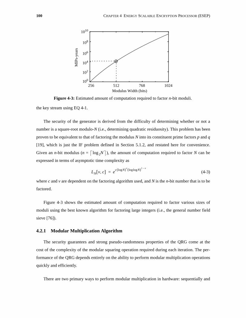
100 CHAPTER 4 ENERGY SCALABLE ENCRYPTION PROCESSOR (ESEP)
the key stream using EQ 4-1.
The security of the generator is derived from the difficulty of determining whether or not a
number is a square-root modulo-N (i.e., determining quadratic residuosity). This problem has been
proven to be equivalent to that of factoring the modulus N into its constituent prime factors p and q
[19], which is just the IF problem defined in Section 5.1.2, and restated here for convenience.
Given an n-bit modulus (n = ), the amount of computation required to factor N can be
expressed in terms of asymptotic time complexity as
(4-3)
where c and v are dependent on the factoring algorithm used, and N is the n-bit number that is to be
factored.
Figure 4-3 shows the estimated amount of computation required to factor various sizes of
moduli using the best known algorithm for factoring large integers (i.e., the general number field
sieve [76]).
4.2.1 Modular Multiplication Algorithm
The security guarantees and strong pseudo-randomness properties of the QRG come at the
cost of the complexity of the modular squaring operation required during each iteration. The per-
formance of the QRG depends entirely on the ability to perform modular multiplication operations
quickly and efficiently.
There are two primary ways to perform modular multiplication in hardware: sequentially and
N2log
LN v c,[ ] ec Nlog( )v
Nloglog( )1 v–
=
Figure 4-3: Estimated amount of computation required to factor n-bit moduli.
256 512 768 1024100
104
108
Modulus Width (bits)
MIP
s-ye
ars
102
106
1010

4.2 QUADRATIC RESIDUE GENERATOR (QRG) 101
concurrently. In a sequential approach, an -bit multiplication is first performed, followed by
a -bit division, where n is on the order of several hundred bits. Unfortunately, the sequential
approach has numerous inefficiencies, such as the fact that the intermediate result requires a 2n-bit
register (more if a redundant representation is used), and generating the intermediate result
requires a time-consuming 2n-bit carry propagate addition (CPA). As a result, the sequential
approach leads to a slow and inefficient implementation. A much more efficient approach is to per-
form the multiplication and division concurrently by performing a partial modular reduction dur-
ing each step of the multiplication algorithm. Using this approach, the intermediate results require
only a few additional digits (e.g., two additional digits [125]) and the results can be kept in a
redundant form for both operations so there is no need for a time-consuming CPA. This leads to a
much more efficient implementation, a fact that is reflected in the predominant use of concurrent
algorithms for performing high-speed modular multiplication (e.g., [21], [72], [88], and [125],
[126]).
Common performance optimizations used in conventional hardware modular multipliers for
RSA-based encryption schemes are not applicable to the QRG as the high overhead costs associ-
ated with common techniques such as Montgomery multiplication (Section 3.4.6), or the Chinese
Remainder Theorem (Section 3.4.7.1) cannot be amortized efficiently in the QRG as only a single
modular multiplication is being performed.
Given the iterative nature of concurrent modular multiplication algorithms (operand sizes on
the order of 512+ bits preclude the use of array implementations), the multiplier’s performance is
dictated by two factors: the number of iterations and the cycle time of each iteration.
The number of iterations required to perform an n-bit modular multiplication is ,
where r is the radix of the multiplication algorithm used. Hence, the multiplication can be sped up
by using a higher radix algorithm. However, for radices above four, multiples of the modulus must
be pre-computed and stored. The resulting overhead and additional circuit complexity offsets any
benefits of utilizing the higher radix. Hence, a radix-4 algorithm was chosen to implement the
QRG.
The cycle time of the multiplier can be significantly reduced by the use of a redundant repre-
sentation that eliminates carry propagation chains. However, the cost of using a redundant repre-
sentation is that at some point, the result must be converted into a non-redundant binary
n n×
2n n×
n r2log⁄

102 CHAPTER 4 ENERGY SCALABLE ENCRYPTION PROCESSOR (ESEP)
representation, which will require a CPA. To maintain high performance, this CPA must be per-
formed in such a way as to remove it from the critical path of the multiplier. In addition, intermedi-
ate results of the algorithm will be in a redundant representation that requires additional storage
elements, and possibly more complex adder structures. Despite these additional costs, the reduc-
tion in critical path proved to be sufficient to reduce the operating voltage of the ESEP such that
the resultant power/energy savings offset these inefficiencies.
The ESEP performs the required modular squaring operation of the QRG using an iterated
radix-4 modular multiplication algorithm based on work by Takagi [125]. The algorithm (Figure
4-4) is essentially a digit-serial multiplication algorithm with an additional partial modular reduc-
tion step being performed each iteration (ALG 4-1).
Input: N: n-bit binary modulusX: n-digit redundant multiplicandY: n-digit redundant multiplier
Output: P: n-digit redundant product (P = XY mod N)
Algorithm: Pn/2+1= 0for (j = floor(n/2); j > -2; j--)
recode Y<2j+1:2j> into YjRj = 4Pj+1 + X·Yjestimate Cj using 8 MSD of Rj and NPj = Rj - 4N·Cj
endforP = P-1/4
Algorithm 4-1: ESEP modular multiplication algorithm
Figure 4-4: Modular multiplication algorithm block diagram.
X·Yj
X Select
X PY
Rj
Y RecoderYj
Cj Selector
N Select
N
4N·Cj
4Pj
Pj+1
shift
8
Cj
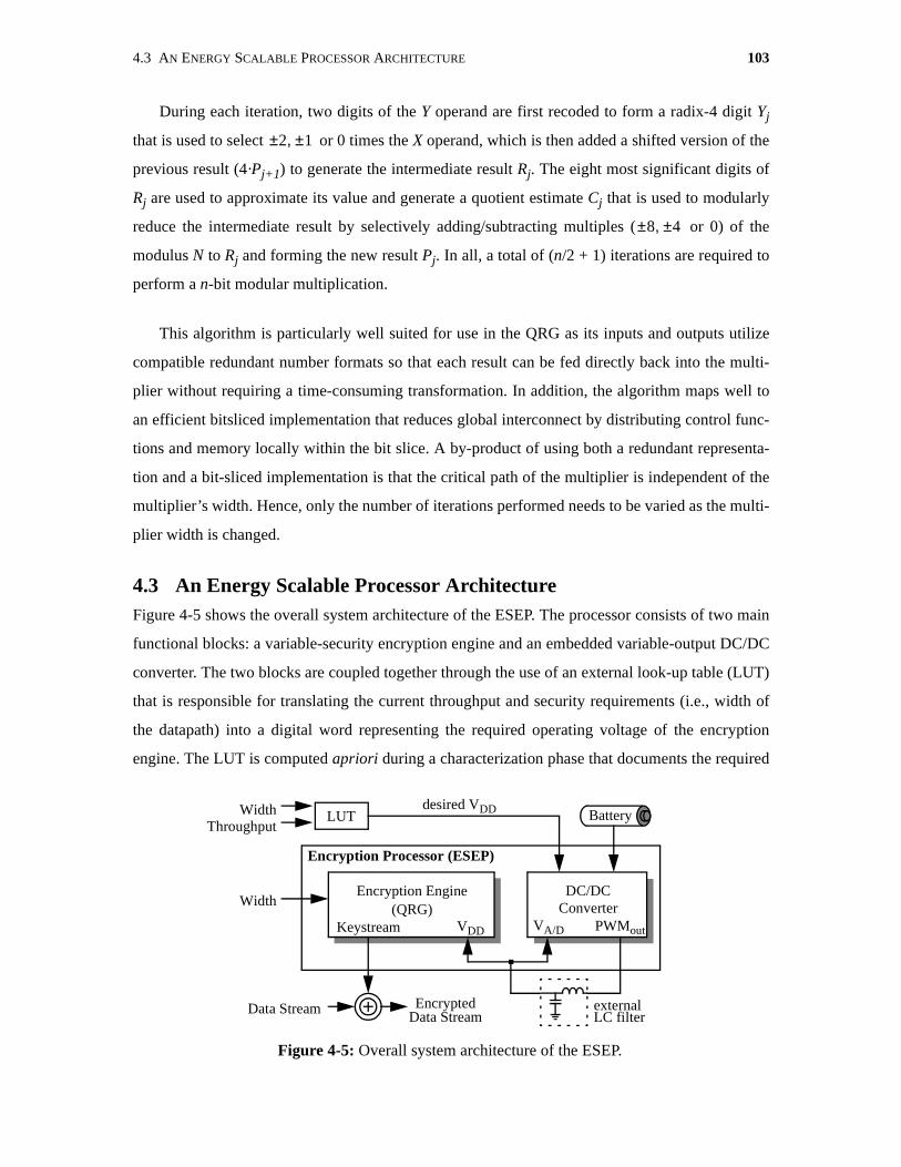
4.3 AN ENERGY SCALABLE PROCESSOR ARCHITECTURE 103
During each iteration, two digits of the Y operand are first recoded to form a radix-4 digit Yj
that is used to select or 0 times the X operand, which is then added a shifted version of the
previous result (4·Pj+1) to generate the intermediate result Rj. The eight most significant digits of
Rj are used to approximate its value and generate a quotient estimate Cj that is used to modularly
reduce the intermediate result by selectively adding/subtracting multiples ( or 0) of the
modulus N to Rj and forming the new result Pj. In all, a total of (n/2 + 1) iterations are required to
perform a n-bit modular multiplication.
This algorithm is particularly well suited for use in the QRG as its inputs and outputs utilize
compatible redundant number formats so that each result can be fed directly back into the multi-
plier without requiring a time-consuming transformation. In addition, the algorithm maps well to
an efficient bitsliced implementation that reduces global interconnect by distributing control func-
tions and memory locally within the bit slice. A by-product of using both a redundant representa-
tion and a bit-sliced implementation is that the critical path of the multiplier is independent of the
multiplier’s width. Hence, only the number of iterations performed needs to be varied as the multi-
plier width is changed.
4.3 An Energy Scalable Processor ArchitectureFigure 4-5 shows the overall system architecture of the ESEP. The processor consists of two main
functional blocks: a variable-security encryption engine and an embedded variable-output DC/DC
converter. The two blocks are coupled together through the use of an external look-up table (LUT)
that is responsible for translating the current throughput and security requirements (i.e., width of
the datapath) into a digital word representing the required operating voltage of the encryption
engine. The LUT is computed apriori during a characterization phase that documents the required
2 1±,±
8 4±,±
Figure 4-5: Overall system architecture of the ESEP.
LUTWidthThroughput
Encryption Processor (ESEP)
Encryption Engine DC/DCConverterWidth
Batterydesired VDD
external
PWMoutVDDKeystream
EncryptedData Stream
(QRG)VA/D
Data Stream LC filter
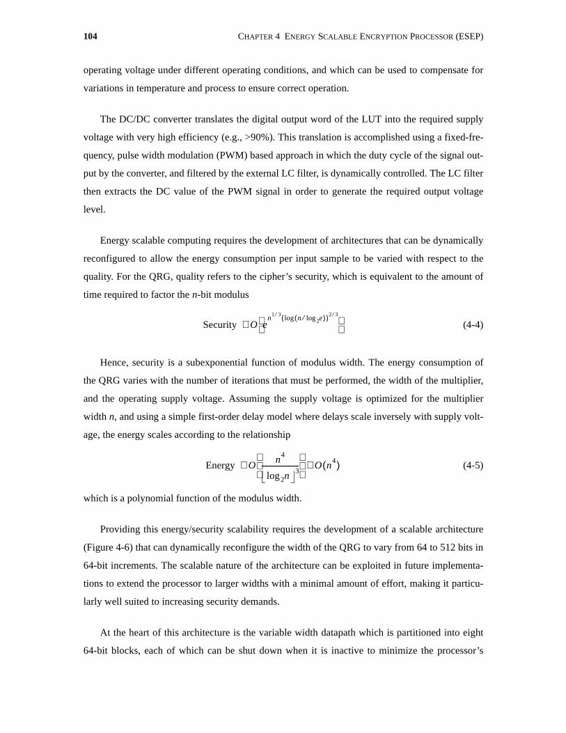
104 CHAPTER 4 ENERGY SCALABLE ENCRYPTION PROCESSOR (ESEP)
operating voltage under different operating conditions, and which can be used to compensate for
variations in temperature and process to ensure correct operation.
The DC/DC converter translates the digital output word of the LUT into the required supply
voltage with very high efficiency (e.g., >90%). This translation is accomplished using a fixed-fre-
quency, pulse width modulation (PWM) based approach in which the duty cycle of the signal out-
put by the converter, and filtered by the external LC filter, is dynamically controlled. The LC filter
then extracts the DC value of the PWM signal in order to generate the required output voltage
level.
Energy scalable computing requires the development of architectures that can be dynamically
reconfigured to allow the energy consumption per input sample to be varied with respect to the
quality. For the QRG, quality refers to the cipher’s security, which is equivalent to the amount of
time required to factor the n-bit modulus
(4-4)
Hence, security is a subexponential function of modulus width. The energy consumption of
the QRG varies with the number of iterations that must be performed, the width of the multiplier,
and the operating supply voltage. Assuming the supply voltage is optimized for the multiplier
width n, and using a simple first-order delay model where delays scale inversely with supply volt-
age, the energy scales according to the relationship
(4-5)
which is a polynomial function of the modulus width.
Providing this energy/security scalability requires the development of a scalable architecture
(Figure 4-6) that can dynamically reconfigure the width of the QRG to vary from 64 to 512 bits in
64-bit increments. The scalable nature of the architecture can be exploited in future implementa-
tions to extend the processor to larger widths with a minimal amount of effort, making it particu-
larly well suited to increasing security demands.
At the heart of this architecture is the variable width datapath which is partitioned into eight
64-bit blocks, each of which can be shut down when it is inactive to minimize the processor’s
Security O en
1 3⁄n e2log⁄( )log( )2 3⁄
∼
Energy On
4
n2log3
----------------------
O n4( )∼ ∼
4.3 AN ENERGY SCALABLE PROCESSOR ARCHITECTURE 105
switched capacitance. By partitioning the datapath in this manner, the energy/power consumption
of the processor can also be allowed to scale with the modulus width, and hence the security
requirements. This form of clock gating is a commonly used technique in low power design. Note
that without clock gating there would still be a reduction in energy consumption due to the reduced
activity of the datapath when it is operating at less than its full width. However, all bits of all regis-
ters would be clocked each cycle leading to a significant amount of unnecessary switched capaci-
tance. Hence, clock gating enables us to eliminate this source of wasted power.
All operands within the datapath are left-aligned on the MSD when the multiplier is operating
at less than its full width. This is a requirement of the algorithm as it handles the MSD in a special
way that requires a modified bitslice in the most significant position.
4.3.1 Global SequencerThe overall operation of the processor is governed by the control functions contained within the
Global Sequencer (GS) block. The sequencer consists of two FSMs, multFSM and initFSM, that
are responsible for generating all of the control and enable signals within the processor. The size of
the operands that are processed, as well as the width of the datapath, is controlled using the
LENGTH<2:0> input to select any of the pre-determined widths (64, 128, 192, 256, 320, 384, 448,
and 512 bits) via the simple formula
. (4-6)
The length is latched at the start of each multiplication or initialization phase, so it need not be
held constant once either operation has begun.
Figure 4-6: Top-level architecture of the encryption engine (QRG).
Dat
apat
h #1
Dat
apat
h #0
Width
Sequencer & I/O Interface
Output Select/Convert
Keystream
Shut Down Control
Dat
apat
h #4
Width
Dat
apat
h #5
Dat
apat
h #3
Dat
apat
h #2
Dat
apat
h #6
Dat
apat
h #7
operand size 64 LENGTH<2:0> 1+( )⋅=
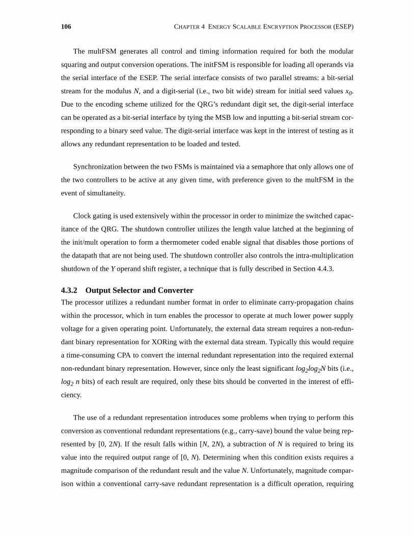
106 CHAPTER 4 ENERGY SCALABLE ENCRYPTION PROCESSOR (ESEP)
The multFSM generates all control and timing information required for both the modular
squaring and output conversion operations. The initFSM is responsible for loading all operands via
the serial interface of the ESEP. The serial interface consists of two parallel streams: a bit-serial
stream for the modulus N, and a digit-serial (i.e., two bit wide) stream for initial seed values x0.
Due to the encoding scheme utilized for the QRG’s redundant digit set, the digit-serial interface
can be operated as a bit-serial interface by tying the MSB low and inputting a bit-serial stream cor-
responding to a binary seed value. The digit-serial interface was kept in the interest of testing as it
allows any redundant representation to be loaded and tested.
Synchronization between the two FSMs is maintained via a semaphore that only allows one of
the two controllers to be active at any given time, with preference given to the multFSM in the
event of simultaneity.
Clock gating is used extensively within the processor in order to minimize the switched capac-
itance of the QRG. The shutdown controller utilizes the length value latched at the beginning of
the init/mult operation to form a thermometer coded enable signal that disables those portions of
the datapath that are not being used. The shutdown controller also controls the intra-multiplication
shutdown of the Y operand shift register, a technique that is fully described in Section 4.4.3.
4.3.2 Output Selector and ConverterThe processor utilizes a redundant number format in order to eliminate carry-propagation chains
within the processor, which in turn enables the processor to operate at much lower power supply
voltage for a given operating point. Unfortunately, the external data stream requires a non-redun-
dant binary representation for XORing with the external data stream. Typically this would require
a time-consuming CPA to convert the internal redundant representation into the required external
non-redundant binary representation. However, since only the least significant log2log2N bits (i.e.,
log2 n bits) of each result are required, only these bits should be converted in the interest of effi-
ciency.
The use of a redundant representation introduces some problems when trying to perform this
conversion as conventional redundant representations (e.g., carry-save) bound the value being rep-
resented by [0, 2N). If the result falls within [N, 2N), a subtraction of N is required to bring its
value into the required output range of [0, N). Determining when this condition exists requires a
magnitude comparison of the redundant result and the value N. Unfortunately, magnitude compar-
ison within a conventional carry-save redundant representation is a difficult operation, requiring
4.3 AN ENERGY SCALABLE PROCESSOR ARCHITECTURE 107
one to essentially eliminate all redundancy through the use of a CPA. Obviously this isn’t very effi-
cient as it will still require all n bits to be converted.
By careful selection of the multiplication algorithm and redundant representation, this ineffi-
ciency can be avoided. In Takagi’s algorithm [125], an extra multiplication iteration enables the
result to be bounded by (N/2, -N/2). Hence, the correction operation that is required in this case is
equivalent to determining if the result is positive or negative. If the result is positive, no correction
is required. Otherwise, the value N needs to be added to the result.
Determining if the result is positive or negative can be computed very efficiently by choosing
the proper redundant representation. By selecting the digit set to be {+1, 0, -1}, the sign of an
operand represented in this digit set can be determined by the sign of the MSD. To facilitate this
computation, the binary encoding shown in Table 4-1 is used, which enables fast negation of oper-
ands using simple inversion and fast sign detection using the MSB. It should be noted that zero is a
special case that needs to be checked for, as 11 isn’t a valid binary representation.
This encoding allows the sign to be computed using the log2n depth tree-based comparator cir-
cuit shown in Figure 4-7. Each node of the tree takes two redundant digits with an implied order-
Digit Binary Value
-1 10
0 00
+1 01
Table 4-1: Binary encoding for ESEP redundant representation.
Figure 4-7: Tree-based comparator circuit for determining sign of result in QRG.
. . .. . .
. . .
. . .
. . .
P Operand Register (n bits)
. . . . . .
input latch
log2n levels
MSB of output is sign
MultDone
<0>
Y<1:0><1>A<1:0>
B<1:0>
<1>
<1>
<0>
<0><1>
<0>
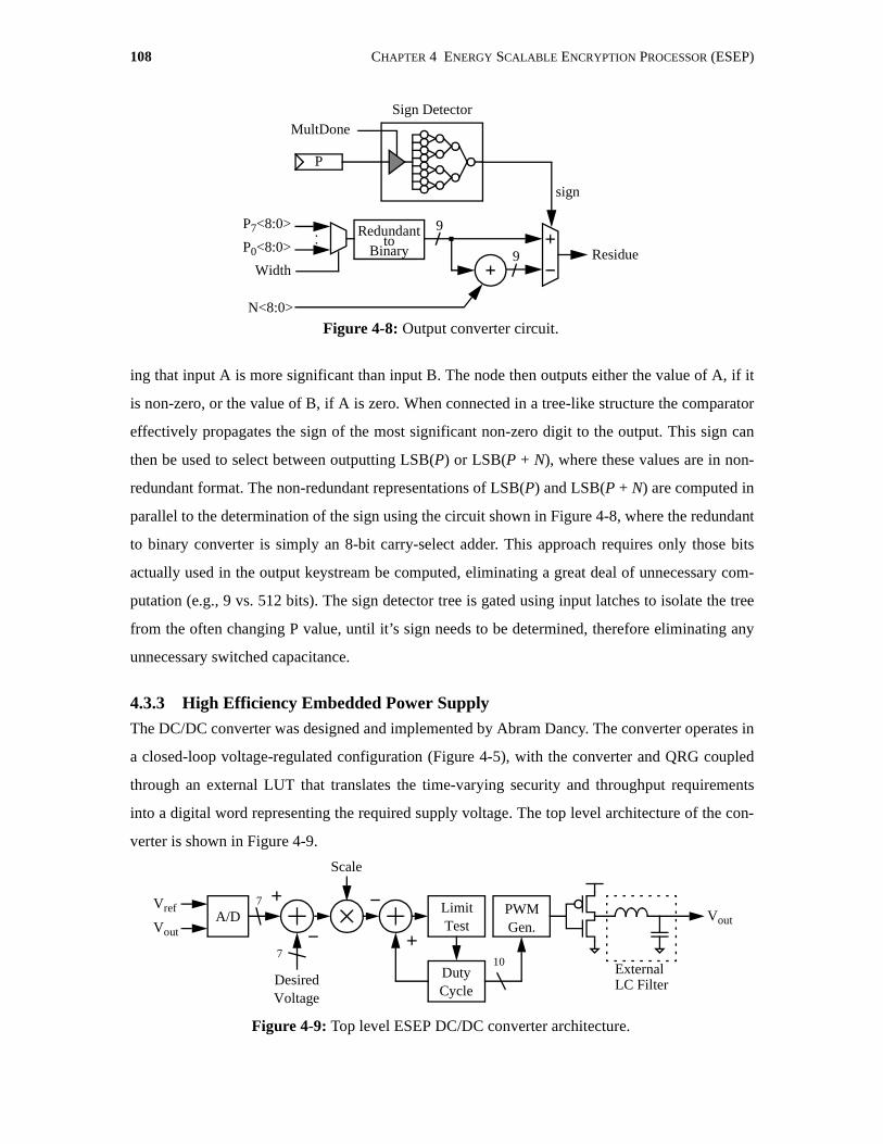
108 CHAPTER 4 ENERGY SCALABLE ENCRYPTION PROCESSOR (ESEP)
ing that input A is more significant than input B. The node then outputs either the value of A, if it
is non-zero, or the value of B, if A is zero. When connected in a tree-like structure the comparator
effectively propagates the sign of the most significant non-zero digit to the output. This sign can
then be used to select between outputting LSB(P) or LSB(P + N), where these values are in non-
redundant format. The non-redundant representations of LSB(P) and LSB(P + N) are computed in
parallel to the determination of the sign using the circuit shown in Figure 4-8, where the redundant
to binary converter is simply an 8-bit carry-select adder. This approach requires only those bits
actually used in the output keystream be computed, eliminating a great deal of unnecessary com-
putation (e.g., 9 vs. 512 bits). The sign detector tree is gated using input latches to isolate the tree
from the often changing P value, until it’s sign needs to be determined, therefore eliminating any
unnecessary switched capacitance.
4.3.3 High Efficiency Embedded Power SupplyThe DC/DC converter was designed and implemented by Abram Dancy. The converter operates in
a closed-loop voltage-regulated configuration (Figure 4-5), with the converter and QRG coupled
through an external LUT that translates the time-varying security and throughput requirements
into a digital word representing the required supply voltage. The top level architecture of the con-
verter is shown in Figure 4-9.
Figure 4-8: Output converter circuit.. .
.P7<8:0>
P0<8:0> Residue
P
sign
MultDoneSign Detector
Width
N<8:0>
Redundantto
Binary
9
9
Figure 4-9: Top level ESEP DC/DC converter architecture.
Scale
DesiredVoltage
LimitTest
DutyCycle
PWMGen.
A/DVref
Vout
7
7
10
Vout
ExternalLC Filter
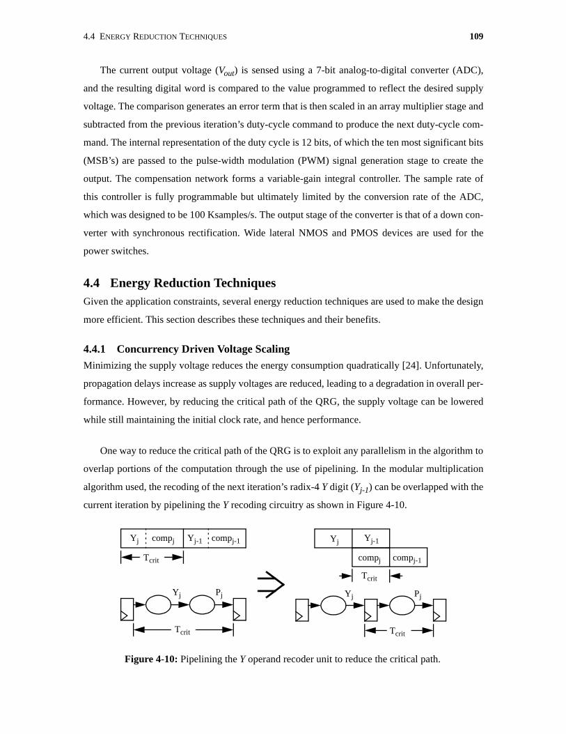
4.4 ENERGY REDUCTION TECHNIQUES 109
The current output voltage (Vout) is sensed using a 7-bit analog-to-digital converter (ADC),
and the resulting digital word is compared to the value programmed to reflect the desired supply
voltage. The comparison generates an error term that is then scaled in an array multiplier stage and
subtracted from the previous iteration’s duty-cycle command to produce the next duty-cycle com-
mand. The internal representation of the duty cycle is 12 bits, of which the ten most significant bits
(MSB’s) are passed to the pulse-width modulation (PWM) signal generation stage to create the
output. The compensation network forms a variable-gain integral controller. The sample rate of
this controller is fully programmable but ultimately limited by the conversion rate of the ADC,
which was designed to be 100 Ksamples/s. The output stage of the converter is that of a down con-
verter with synchronous rectification. Wide lateral NMOS and PMOS devices are used for the
power switches.
4.4 Energy Reduction TechniquesGiven the application constraints, several energy reduction techniques are used to make the design
more efficient. This section describes these techniques and their benefits.
4.4.1 Concurrency Driven Voltage ScalingMinimizing the supply voltage reduces the energy consumption quadratically [24]. Unfortunately,
propagation delays increase as supply voltages are reduced, leading to a degradation in overall per-
formance. However, by reducing the critical path of the QRG, the supply voltage can be lowered
while still maintaining the initial clock rate, and hence performance.
One way to reduce the critical path of the QRG is to exploit any parallelism in the algorithm to
overlap portions of the computation through the use of pipelining. In the modular multiplication
algorithm used, the recoding of the next iteration’s radix-4 Y digit (Yj-1) can be overlapped with the
current iteration by pipelining the Y recoding circuitry as shown in Figure 4-10.
Figure 4-10: Pipelining the Y operand recoder unit to reduce the critical path.
Yj compj Yj-1 compj-1
Tcrit compj
Tcrit
compj-1
Yj-1Yj
Yj Pj
Tcrit
Pj
Tcrit
Yj

110 CHAPTER 4 ENERGY SCALABLE ENCRYPTION PROCESSOR (ESEP)
The critical path can also be reduced by accelerating the determination of the quotient estimate
Cj. A naive approach to computing Cj requires three time-consuming carry-propagate additions. A
much more time-efficient approach takes advantage of the fact that only the signs of these interme-
diate results are required. Hence, a fast carry-lookahead based sign generator circuit can be used to
generate these sign bits in parallel (Figure 4-11). The sign bits are then decoded using a single
level of logic to form the quotient estimate, Cj.
Using these techniques, the critical path of the QRG was reduced by 27%, allowing the supply
voltage to be reduced from 2.9 to 2.5V, for a total energy reduction of 23%.
4.4.2 Self-timed Gating
A major source of unnecessary switched capacitance in a large datapath such as bit-sliced adders
and multipliers, is due to spurious transitions caused by glitch propagation. In a design such as the
ESEP, which is dominated almost entirely by a very wide datapath, spurious transitions can lead to
substantial wasted energy consumption (e.g., 20% of the total energy). Hence, it is imperative that
they be minimized.
One approach that has already been utilized in the ESEP for minimizing spurious transitions is
the elimination of carry-propagation chains through the use of redundant representations (a nice
beneficial side-effect!). Another deliberate approach is the use of self-timed techniques such as
those commonly used in memory designs for control signal generation, or multipliers for power
reduction [112]. A self-timed gating approach is used to partition each algorithm iteration into
three distinct computational phases (Figure 4-12). Tri-state buffers are inserted between each of
these phases to prevent glitches from propagating further in the datapath. The buffers are enabled,
and the computation allowed to proceed only when the inputs are ensured to be stable and valid.
This is determined by the use of a self-timed enable signal which is generated by passing the sys-
tem clock through a delay chain that models the critical path of the processor. The delay chain is
Figure 4-11: Optimizing and parallelizing the quotient estimation unit to reduce critical path.
R<7:0>
Nmsb<4:0>
(6·N)msb<4:0>
cout
cout
(R)msb
Sig
nD
ecod
er
Cj
ΦCj
Sign Generator
Red ⇒ Bin
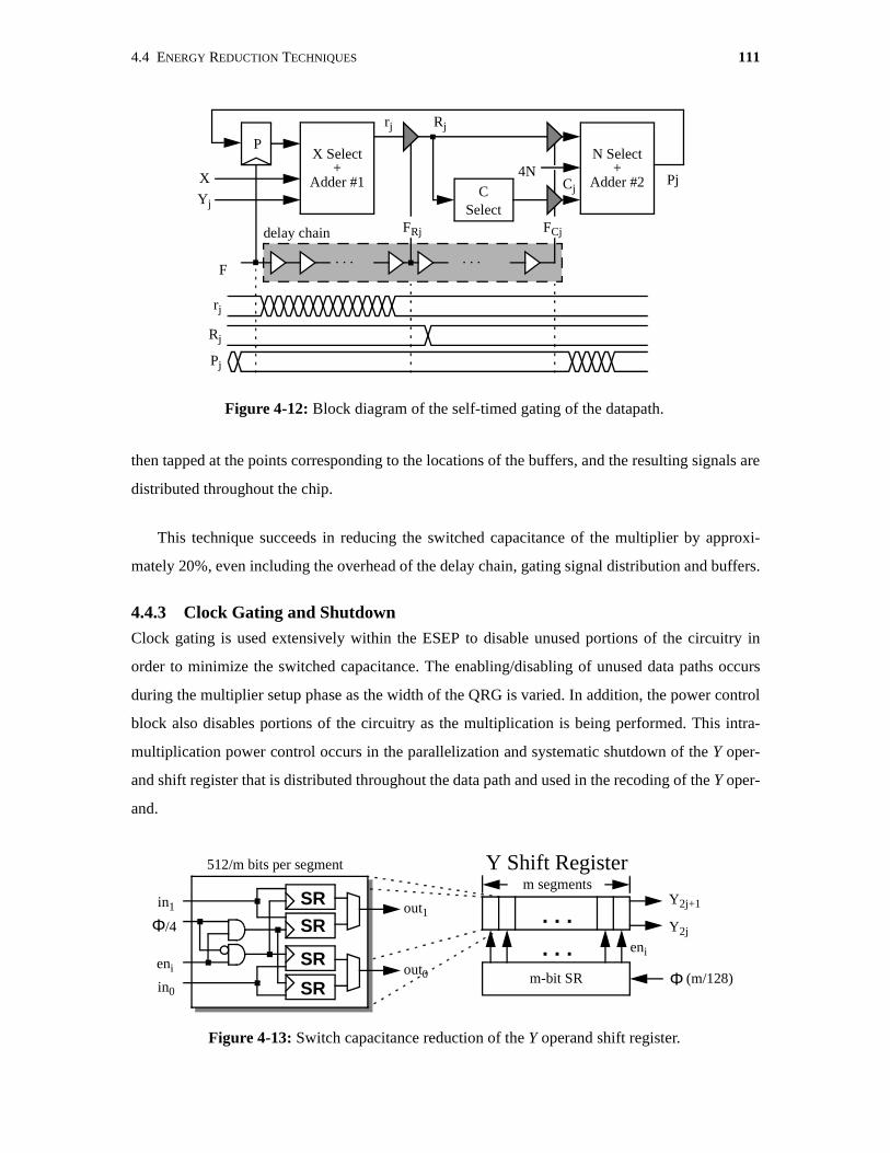
4.4 ENERGY REDUCTION TECHNIQUES 111
then tapped at the points corresponding to the locations of the buffers, and the resulting signals are
distributed throughout the chip.
This technique succeeds in reducing the switched capacitance of the multiplier by approxi-
mately 20%, even including the overhead of the delay chain, gating signal distribution and buffers.
4.4.3 Clock Gating and ShutdownClock gating is used extensively within the ESEP to disable unused portions of the circuitry in
order to minimize the switched capacitance. The enabling/disabling of unused data paths occurs
during the multiplier setup phase as the width of the QRG is varied. In addition, the power control
block also disables portions of the circuitry as the multiplication is being performed. This intra-
multiplication power control occurs in the parallelization and systematic shutdown of the Y oper-
and shift register that is distributed throughout the data path and used in the recoding of the Y oper-
and.
Figure 4-12: Block diagram of the self-timed gating of the datapath.
P
C
Rj
4NN Select
+Adder #2
X Select+
Adder #1X
Yj
FRj FCj
. . .. . .F
delay chain
Pj
Rj
rj
rj
Pj
Select
Cj
Figure 4-13: Switch capacitance reduction of the Y operand shift register.
. . .Φm-bit SR
. . .eni
512/m bits per segment Y Shift Registerm segments
(m/128)
Y2j+1
Y2j
SR
SR
SR
SR
out1
out0
in1
eni
in0
Φ/4
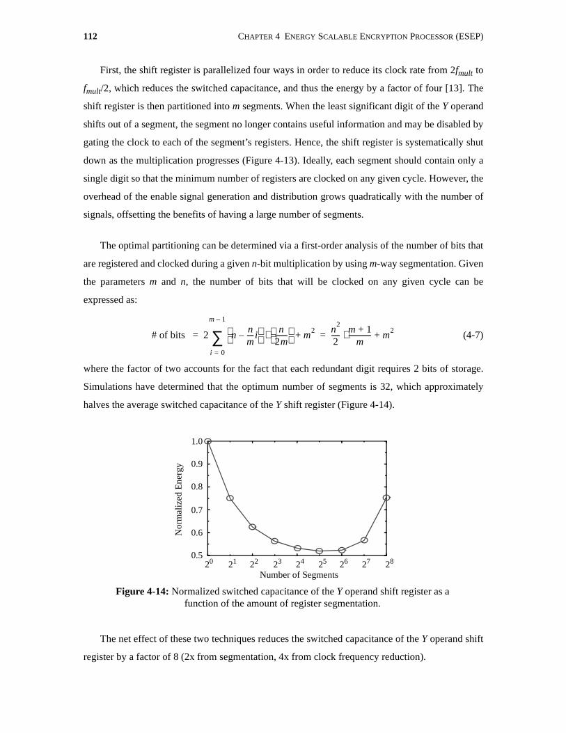
112 CHAPTER 4 ENERGY SCALABLE ENCRYPTION PROCESSOR (ESEP)
First, the shift register is parallelized four ways in order to reduce its clock rate from 2fmult to
fmult/2, which reduces the switched capacitance, and thus the energy by a factor of four [13]. The
shift register is then partitioned into m segments. When the least significant digit of the Y operand
shifts out of a segment, the segment no longer contains useful information and may be disabled by
gating the clock to each of the segment’s registers. Hence, the shift register is systematically shut
down as the multiplication progresses (Figure 4-13). Ideally, each segment should contain only a
single digit so that the minimum number of registers are clocked on any given cycle. However, the
overhead of the enable signal generation and distribution grows quadratically with the number of
signals, offsetting the benefits of having a large number of segments.
The optimal partitioning can be determined via a first-order analysis of the number of bits that
are registered and clocked during a given n-bit multiplication by using m-way segmentation. Given
the parameters m and n, the number of bits that will be clocked on any given cycle can be
expressed as:
(4-7)
where the factor of two accounts for the fact that each redundant digit requires 2 bits of storage.
Simulations have determined that the optimum number of segments is 32, which approximately
halves the average switched capacitance of the Y shift register (Figure 4-14).
The net effect of these two techniques reduces the switched capacitance of the Y operand shift
register by a factor of 8 (2x from segmentation, 4x from clock frequency reduction).
# of bits 2 nnm---- i–
n2m-------
⋅ m2+
i 0=
m 1–
∑ n2
2-----
m 1+m
------------- m2+⋅= =
Figure 4-14: Normalized switched capacitance of the Y operand shift register as afunction of the amount of register segmentation.
Nor
mal
ized
Ene
rgy
Number of Segments
0.5
0.6
0.7
0.8
0.9
1.0
20 21 22 23 24 25 26 27 28
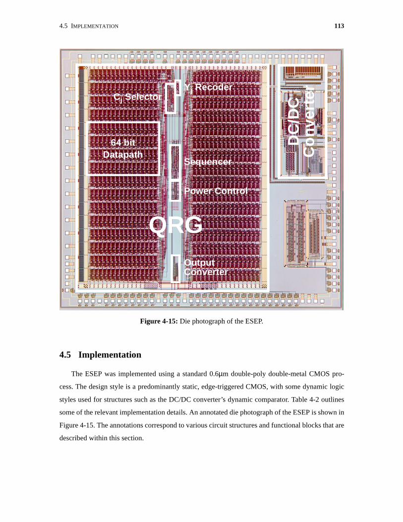
4.5 IMPLEMENTATION 113
4.5 Implementation
The ESEP was implemented using a standard 0.6µm double-poly double-metal CMOS pro-
cess. The design style is a predominantly static, edge-triggered CMOS, with some dynamic logic
styles used for structures such as the DC/DC converter’s dynamic comparator. Table 4-2 outlines
some of the relevant implementation details. An annotated die photograph of the ESEP is shown in
Figure 4-15. The annotations correspond to various circuit structures and functional blocks that are
described within this section.
Figure 4-15: Die photograph of the ESEP.
64 bit
Power Control
Output
Sequencer
Cj SelectorYj Recoder
Datapath
Converter
QRG
DC
/DC
Co
nve
rter
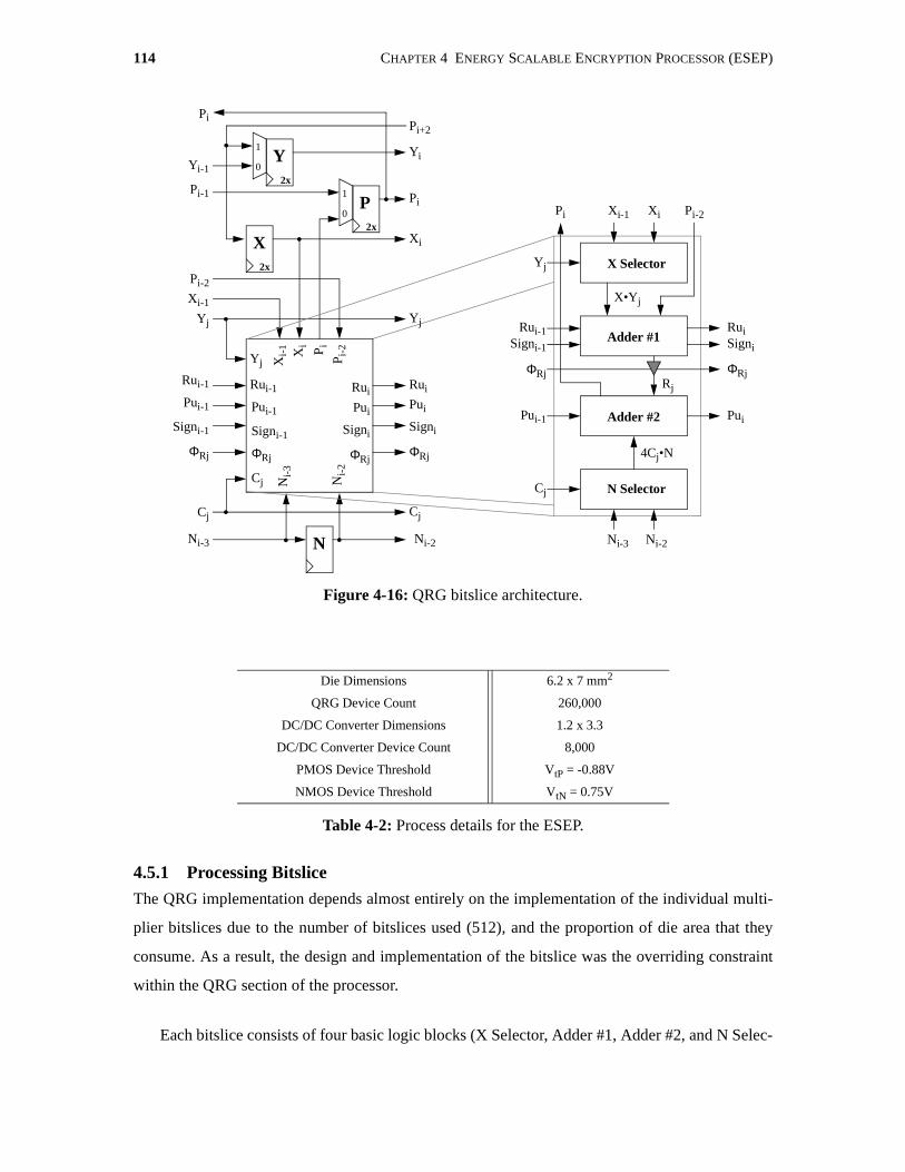
114 CHAPTER 4 ENERGY SCALABLE ENCRYPTION PROCESSOR (ESEP)
4.5.1 Processing Bitslice
The QRG implementation depends almost entirely on the implementation of the individual multi-
plier bitslices due to the number of bitslices used (512), and the proportion of die area that they
consume. As a result, the design and implementation of the bitslice was the overriding constraint
within the QRG section of the processor.
Each bitslice consists of four basic logic blocks (X Selector, Adder #1, Adder #2, and N Selec-
Die Dimensions 6.2 x 7 mm2
QRG Device Count 260,000
DC/DC Converter Dimensions 1.2 x 3.3
DC/DC Converter Device Count 8,000
PMOS Device Threshold VtP = -0.88V
NMOS Device Threshold VtN = 0.75V
Table 4-2: Process details for the ESEP.
Figure 4-16: QRG bitslice architecture.
1
0
1
0
2x
2x
2x
Y
P
X
N
Yi-1
Pi-1
Ni-3
Xi-
1 Xi
Pi-
2Pi
Xi-1
Pi-2
Ni-
2
Ni-
3
Pi
Yi
Xi
Yj Yj
Cj Cj
Rui-1
Pui-1
Signi-1
Rui
Pui
Signi
ΦRj ΦRj
Pi+2
Pi
Rui
Pui
Signi
ΦRj
Rui-1
Pui-1
Signi-1
ΦRj
Yj
Cj
Ni-2
4Cj•N
Rj
ΦRj ΦRj
Adder #1
N Selector
X SelectorYj
Cj
X•Yj
Pi-2Pi
Rui
Adder #2 Pui
Rui-1
Pui-1
Ni-3
Xi-1 Xi
Ni-2
SigniSigni-1
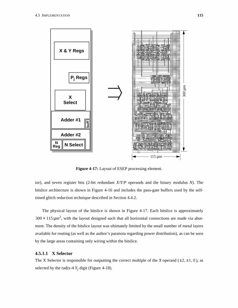
4.5 IMPLEMENTATION 115
tor), and seven register bits (2-bit redundant X/Y/P operands and the binary modulus N). The
bitslice architecture is shown in Figure 4-16 and includes the pass-gate buffers used by the self-
timed glitch reduction technique described in Section 4.4.2.
The physical layout of the bitslice is shown in Figure 4-17. Each bitslice is approximately
µm2, with the layout designed such that all horizontal connections are made via abut-
ment. The density of the bitslice layout was ultimately limited by the small number of metal layers
available for routing (as well as the author’s paranoia regarding power distribution), as can be seen
by the large areas containing only wiring within the bitslice.
4.5.1.1 X SelectorThe X Selector is responsible for outputting the correct multiple of the X operand ( ), as
selected by the radix-4 Yj digit (Figure 4-18).
300 115×
Figure 4-17: Layout of ESEP processing element.
X & Y Regs
Pj Regs
Adder #1
Adder #2
X
N Select
Select
bu
ff
NReg
300
µm
115 µm
2 1 0,±,±

116 CHAPTER 4 ENERGY SCALABLE ENCRYPTION PROCESSOR (ESEP)
4.5.1.2 Redundant Adder #1The first redundant adder is responsible for adding the X Selector’s output value (XYj) to a shifted
version of the previous partial product value (Pj+1). The shifting of Pj+1 has the same effect as
multiplication by 4. The adder formulates its output by performing a two-phase accumulation in
which the values Rti and Rui+1 are first computed, and then the value Ri is computed by adding Rti
and Rui together (Figure 4-19).
4.5.1.3 N Selector
The N Selector utilizes the quotient estimate, Cj, to select a multiple of the modulus N that is sub-
tracted from the value Rj within the second redundant adder in order to perform the partial modular
reduction. In comparison, the N Selector is decidedly less complex than the X Selector as the mod-
ulus N is in a non-redundant binary representation, so its output is a simple multiplex/invert opera-
tion (Figure 4-20).
Figure 4-18: X selector implementation.
Yj
110 (-2)101 (-1)000 001 (+1)010 (+2)
X•Yj
-Xi-1 (-2X)-Xi (-X)
0Xi (+X)
Xi-1 (+2X)
Xi
Xi-1
XYi
Yj
3
0
-2+20
+1-1
Xi
Yj
X Selector
22 2
2
Figure 4-19: Redundant Adder #1 implementation.
0-1/1
0
-1/10
-1/1
0-1/1
0
-101
10-1
P i-2
YXi
01/01
0/-10
-1/0
-10/-1
0
-101
10-1
P i-2
YXi
Rti
Rui+1
Pi-2 X·Yi
ΦRj
Bitslicei
Ru Rt
Pi-2 X·Yi
ΦRj
Ru Rt
Bitslicei-1
. . .. . .Rui+1
RtiRui
Ri
Rti-1
Rui-1
Ri-1
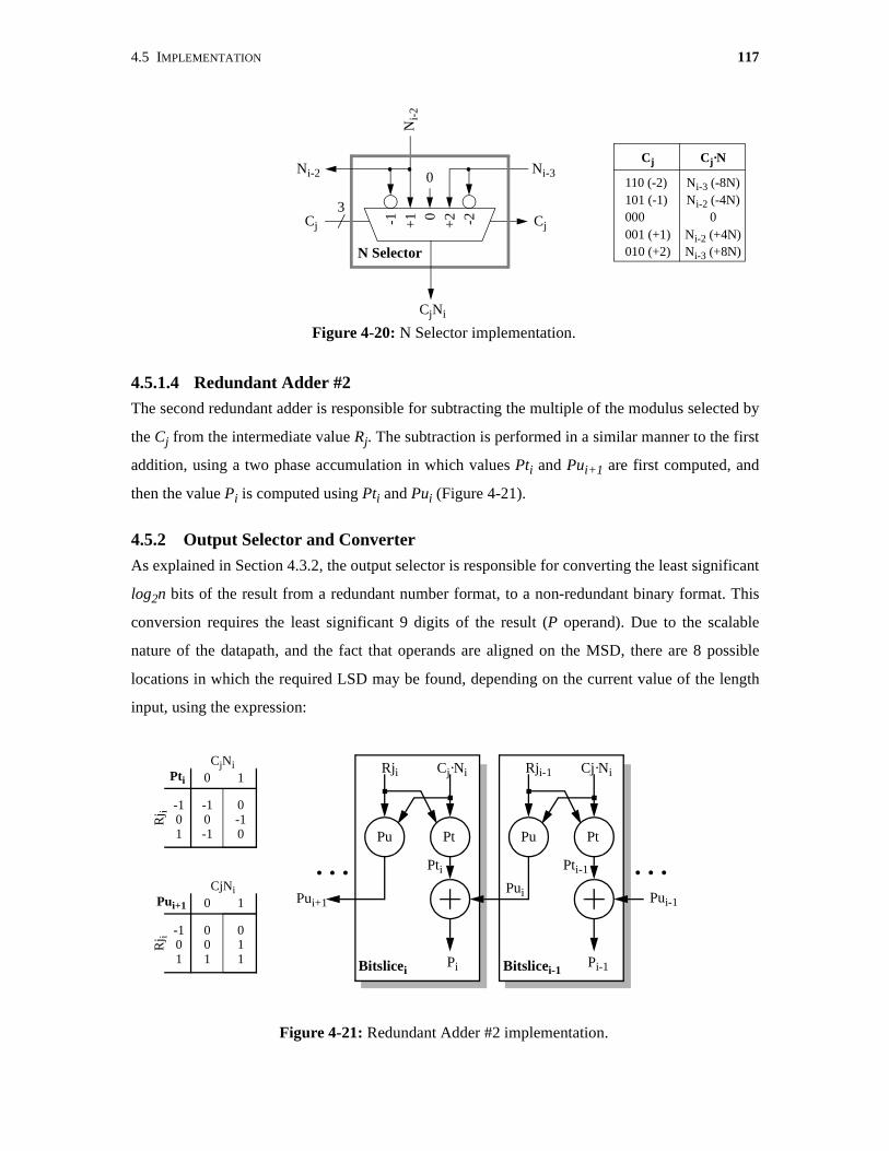
4.5 IMPLEMENTATION 117
4.5.1.4 Redundant Adder #2The second redundant adder is responsible for subtracting the multiple of the modulus selected by
the Cj from the intermediate value Rj. The subtraction is performed in a similar manner to the first
addition, using a two phase accumulation in which values Pti and Pui+1 are first computed, and
then the value Pi is computed using Pti and Pui (Figure 4-21).
4.5.2 Output Selector and Converter
As explained in Section 4.3.2, the output selector is responsible for converting the least significant
log2n bits of the result from a redundant number format, to a non-redundant binary format. This
conversion requires the least significant 9 digits of the result (P operand). Due to the scalable
nature of the datapath, and the fact that operands are aligned on the MSD, there are 8 possible
locations in which the required LSD may be found, depending on the current value of the length
input, using the expression:
Figure 4-20: N Selector implementation.
Cj
110 (-2)101 (-1)000 001 (+1)010 (+2)
Cj·N
Ni-3 (-8N)Ni-2 (-4N)
0Ni-2 (+4N)Ni-3 (+8N)
Ni-
2
Ni-3
CjNi
Cj
3
0
-2+20
+1-1
Ni-2
Cj
N Selector
Figure 4-21: Redundant Adder #2 implementation.
0-10
-10-1
-101
10
Rj i
CjNiPti
011
001
-101
10
Rj i
CjNiPui+1
Rji Cj·Ni
Bitslicei
Pu Pt
Rji-1 Cj·Ni
Pu Pt
Bitslicei-1
. . .. . .Pui+1
PtiPui
Pi
Pti-1
Pui-1
Pi-1
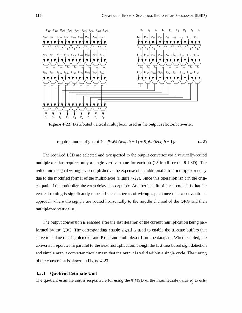
118 CHAPTER 4 ENERGY SCALABLE ENCRYPTION PROCESSOR (ESEP)
required output digits of P = P<64·(length + 1) + 8, 64·(length + 1)> (4-8)
The required LSD are selected and transported to the output converter via a vertically-routed
multiplexor that requires only a single vertical route for each bit (18 in all for the 9 LSD). The
reduction in signal wiring is accomplished at the expense of an additional 2-to-1 multiplexor delay
due to the modified format of the multiplexor (Figure 4-22). Since this operation isn’t in the criti-
cal path of the multiplier, the extra delay is acceptable. Another benefit of this approach is that the
vertical routing is significantly more efficient in terms of wiring capacitance than a conventional
approach where the signals are routed horizontally to the middle channel of the QRG and then
multiplexed vertically.
The output conversion is enabled after the last iteration of the current multiplication being per-
formed by the QRG. The corresponding enable signal is used to enable the tri-state buffers that
serve to isolate the sign detector and P operand multiplexor from the datapath. When enabled, the
conversion operates in parallel to the next multiplication, though the fast tree-based sign detection
and simple output converter circuit mean that the output is valid within a single cycle. The timing
of the conversion is shown in Figure 4-23.
4.5.3 Quotient Estimate UnitThe quotient estimate unit is responsible for using the 8 MSD of the intermediate value Rj to esti-
Figure 4-22: Distributed vertical multiplexor used in the output selector/converter.
P384 P385 P386 P387 P388 P389 P390 P391
P448 P449 P450 P451 P452 P453 P454 P455
P320 P321 P322 P323 P324 P325 P326 P327
P256 P257 P258 P259 P260 P261 P262 P263 P192 P193 P194 P195 P196 P197 P198 P199
P128 P129 P130 P131 P132 P133 P134 P135
P64 P65 P66 P67 P68 P69 P70 P71
P0 P1 P2 P3 P4 P5 P6 P7
P0 P1 P2 P3 P4 P5 P6 P7
P392
P456
P328
P264
P8
P200
P136
P72
P8

4.5 IMPLEMENTATION 119
mate the multiple of the modulus N required to modularly reduce the intermediate value during
each iteration of the multiplication described in ALG 4-1.
To ensure efficient computation, an approximation must be made to avoid having to perform a
full division operation. This approximation introduces errors to the computation, but Takagi [125]
has shown that by utilizing the 8 MSD of Rj, and an additional iteration of the multiplication algo-
rithm, the error can be controlled to the point where the final result requires at most one extra addi-
tion to correct any error that it might have.
The quotient estimation, Cj, is formed using the functional mapping:
where top(Rj) is the non-redundant representation of the 8 MSD of Rj, top(2N) is the 5 MSB of 2N,
and top(6N) is the 7 MSB of 6N. The top(6N) term is formed using a bit-serial adder during the
loading of the N operand, thereby hiding the computation in its entirety.
The quotient estimator first computes top(Rj) using an 8-bit carry-select adder partitioned into
two 4-bit computations for a total delay of 5 gate delays. The carry-out of the adder forms the first
(S0) of three sign bits used to determine Cj. top(Rj) is then compared to both top(2N) and -top(2N)
by adding the values together using a pseudo-adder that utilizes fast carry-lookahead techniques to
compute only the sign of the result. A multiplexor is then used to select the appropriate result, as
determined by the sign output of the adder that computes top(Rj). If the sign is positive then the
Figure 4-23: Operation and timing of the output conversion circuit.
CLK
MultiplierIteration
Enable
0 -1 loading operands
Detector/Mux
Sign ValidSign DetectorOutput
ValidBinaryOutput
Cj
2 top Rj( ) top 6N( )–<,–
1 top 6N( ) top Rj( ) top 2N( )–<≤–,–
0 top 2N( ) top Rj( ) top 2N( )<≤–, 1 top 2N( ) top Rj( ) top 6N( )<≤, 2 top 6N( ) top Rj( )≤,
=

120 CHAPTER 4 ENERGY SCALABLE ENCRYPTION PROCESSOR (ESEP)
comparison to -top(2N) is used, otherwise the comparison to top(2N) is selected to become S1. The
same operation is performed concurrently to compare top(Rj) to +/- top(6N) and determine S2.
Table 4-3 shows the decoding of the resulting sign bits (S2:0) that is used to determine the quotient
estimate Cj.
4.5.4 Y RecoderThe Y Recoder is responsible for recoding two digits from the radix-2 Y operand into the radix-4
Yj digit used by the X Selector circuitry of the datapath. The recoding is done in two stages: first
the intermediate values Yu and Yt are computed using the three most significant bits of the Y oper-
and shift register (i.e., bits Y<2j+1,2j,2j-1>). These values are combined to form Yj using a simple
addition. As described in Section 4.4.1, the operation is pipelined to allow Yj to be computed in
parallel to the multiplier iteration Yj+1. The resulting implementation of the Y Recoder is shown in
Figure 4-24.
Sign Bits (S2S1S0) Interpretation Cj
000 010 (2)
001 000 (0)
010 Not possible N/A
011 101 (-1)
100 001 (1)
101 Not possible N/A
110 000 (0)
111 110 (-2)
Table 4-3: Quotient estimate decoding.
top Rj( ) top 6N( )≥
top 2N( ) top Rj( ) 0<≤–
top 2N( ) top Rj( ) top 6N( )–≥>–
top 2N( ) top Rj( ) top 6N( )<≤
0 top Rj( ) top 2N( )<≤
top Rj( ) top 6N( )–<
Figure 4-24: Y Recoder implementation.
001
0/-10
1/0
-100
-101
10-1
Y2j
+1
Y2j
-11-1
-2/20
-2/2
1-11
-101
10-1
Y2j
+1
Y2j
Yti
Yui+1
“x/y” = y if (Y2j-1 < 0), x otherwise
Yt
Yu
x2 x2 x2
Y 2j-1
Recoded
Y 2j+1
x3
Yj
Y 2j

4.5 IMPLEMENTATION 121
4.5.5 Controller LogicThe controller logic consists of the global sequencer and I/O interface control circuitry, the shut-
down controller, as well as any additional control logic used by the QRG (e.g., tapped delay line
and drivers used for the self-timed gating of the datapath). The logic is very straightforward and
consists entirely of random combinational logic, and edge-triggered flip flops.
4.5.6 Variable Output DC/DC ConverterThe converter utilizes a very power and area efficient hybrid delay-line/counter-based to generate
the required PWM signal for the output power switches. In the past, PWM signal generation has
been performed in an all digital manner using either fast-clocked counters [132] or a pure delay-
line based approach [33].
Fast clocked counters partition the switching interval into 2m sub-intervals using a m-bit down
counter and zero detector (Figure 4-25). At the beginning of each switching interval, the output
flip-flop is set and the counter is loaded with the duty-cycle command word. The counter counts
down to zero, at which point the flip-flop is reset. Unfortunately, the counter clock frequency is 2m
times the switching frequency, which implies high power dissipation (on the order of several milli-
watts [132]) and thus low efficiencies under low output power conditions.
A pure delay-line based approach (Figure 4-26) partitions the switching interval into 2m sub-
intervals using a tapped-delay line containing 2m variable delay elements (e.g., current-starved
inverters). The total delay of the line is made equal to the switching interval of the supply through
the use of a delay-locked loop (DLL) so that the output of the kth delay element occurs k/2mth of
the way through the switching interval. The delay-matching network is used to offset the propaga-
tion delay of the multiplexor. The disadvantage of this approach is that it requires a 2m-to-1 multi-
plexor in order to gate the required delay-line tap to the reset input of the output flip-flop, which
can require a substantial amount of area as m increases.
Figure 4-25: Fast-clocked counter based approach for PWM signal generation.
Data
cnt down
Duty Cycle
S
RPWM Output
Φcnt = 2n·Φswitch
Φswitch Load Datan
QOut . .
.
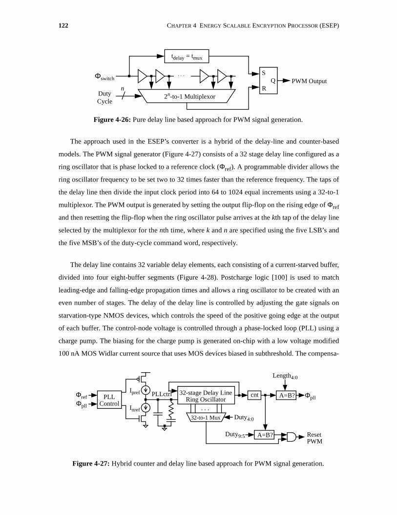
122 CHAPTER 4 ENERGY SCALABLE ENCRYPTION PROCESSOR (ESEP)
The approach used in the ESEP’s converter is a hybrid of the delay-line and counter-based
models. The PWM signal generator (Figure 4-27) consists of a 32 stage delay line configured as a
ring oscillator that is phase locked to a reference clock (Φref). A programmable divider allows the
ring oscillator frequency to be set two to 32 times faster than the reference frequency. The taps of
the delay line then divide the input clock period into 64 to 1024 equal increments using a 32-to-1
multiplexor. The PWM output is generated by setting the output flip-flop on the rising edge of Φref
and then resetting the flip-flop when the ring oscillator pulse arrives at the kth tap of the delay line
selected by the multiplexor for the nth time, where k and n are specified using the five LSB’s and
the five MSB’s of the duty-cycle command word, respectively.
The delay line contains 32 variable delay elements, each consisting of a current-starved buffer,
divided into four eight-buffer segments (Figure 4-28). Postcharge logic [100] is used to match
leading-edge and falling-edge propagation times and allows a ring oscillator to be created with an
even number of stages. The delay of the delay line is controlled by adjusting the gate signals on
starvation-type NMOS devices, which controls the speed of the positive going edge at the output
of each buffer. The control-node voltage is controlled through a phase-locked loop (PLL) using a
charge pump. The biasing for the charge pump is generated on-chip with a low voltage modified
100 nA MOS Widlar current source that uses MOS devices biased in subthreshold. The compensa-
Figure 4-26: Pure delay line based approach for PWM signal generation.
2n-to-1 Multiplexor
S
RQ PWM Output
tdelay = tmux
. . .
nDutyCycle
Φswitch
Figure 4-27: Hybrid counter and delay line based approach for PWM signal generation.
PLLControl
32-stage Delay LineRing Oscillator
ΦrefΦpll
cnt A=B?
A=B?
32-to-1 Mux
. . .
Duty4:0
Duty9:5
Length4:0
Reset
Φpll
PWM
PLLctrlIpref
Inref

4.5 IMPLEMENTATION 123
tion network of the PLL is also implemented on-chip using poly-poly capacitors and a poly resis-
tor.
The hybrid approach provides considerable advantages over both of the aforementioned tech-
niques. By using a delay line, the circuit can be clocked at a much lower rate than in the fast-
clocked counter approach, resulting in a 32x reduction in power. This enables significantly higher
efficiencies at low load power levels. The use of the counter enables the size of the delay line to be
reduced so that the width requirements of the selection multiplexor can be reduced by a factor of
eight relative to the pure delay-line implementation (assuming 256 taps). This yields a 9x reduc-
tion in area relative to the pure delay line based approach.
The ADC is a 100 Ksample/s, 7 bit, charge-redistribution converter. The advantage of a charge
redistribution converter for low-power applications is that it can be implemented without amplifi-
ers, which would typically cause significant static power to be dissipated. A dynamic comparator
is utilized to compare the capacitor array voltage to an external analog reference at each stage of
the conversion. The dynamic comparator dissipates power only during evaluations and requires no
external biasing networks.
An annotated die photograph of the DC/DC Converter is shown in Figure 4-29. The converter
measures approximately 3 x 1.8 mm2. The size is somewhat misleading, as portions of its circuitry
are dedicated to test structures used to characterize this prototype implementation, and could be
eliminated in future implementations.
Figure 4-28: The ESEP’s PWM signal generator delay line.
Reset
In
Reset
In
Reset
In
Reset
In
Reset
InTap31
. . . . . . . . .
. . .. . .
Tap0 Tap1:6 Tap7 Tap8:15 Tap16
Tap27Tap11
OutReset
In
PLLctrl
Tap19
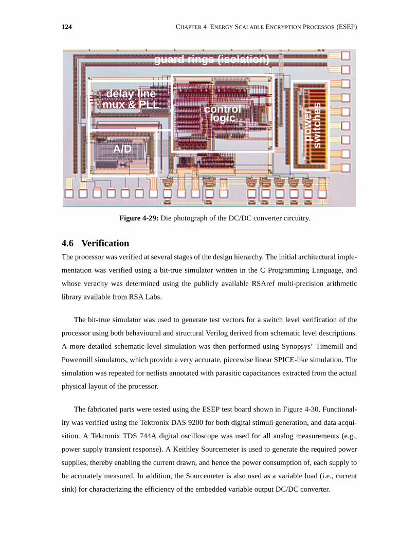
124 CHAPTER 4 ENERGY SCALABLE ENCRYPTION PROCESSOR (ESEP)
4.6 VerificationThe processor was verified at several stages of the design hierarchy. The initial architectural imple-
mentation was verified using a bit-true simulator written in the C Programming Language, and
whose veracity was determined using the publicly available RSAref multi-precision arithmetic
library available from RSA Labs.
The bit-true simulator was used to generate test vectors for a switch level verification of the
processor using both behavioural and structural Verilog derived from schematic level descriptions.
A more detailed schematic-level simulation was then performed using Synopsys’ Timemill and
Powermill simulators, which provide a very accurate, piecewise linear SPICE-like simulation. The
simulation was repeated for netlists annotated with parasitic capacitances extracted from the actual
physical layout of the processor.
The fabricated parts were tested using the ESEP test board shown in Figure 4-30. Functional-
ity was verified using the Tektronix DAS 9200 for both digital stimuli generation, and data acqui-
sition. A Tektronix TDS 744A digital oscilloscope was used for all analog measurements (e.g.,
power supply transient response). A Keithley Sourcemeter is used to generate the required power
supplies, thereby enabling the current drawn, and hence the power consumption of, each supply to
be accurately measured. In addition, the Sourcemeter is also used as a variable load (i.e., current
sink) for characterizing the efficiency of the embedded variable output DC/DC converter.
Figure 4-29: Die photograph of the DC/DC converter circuitry.
guard rings (isolation)
po
wer
swit
chescontrol
logic
A/D
delay linemux & PLL
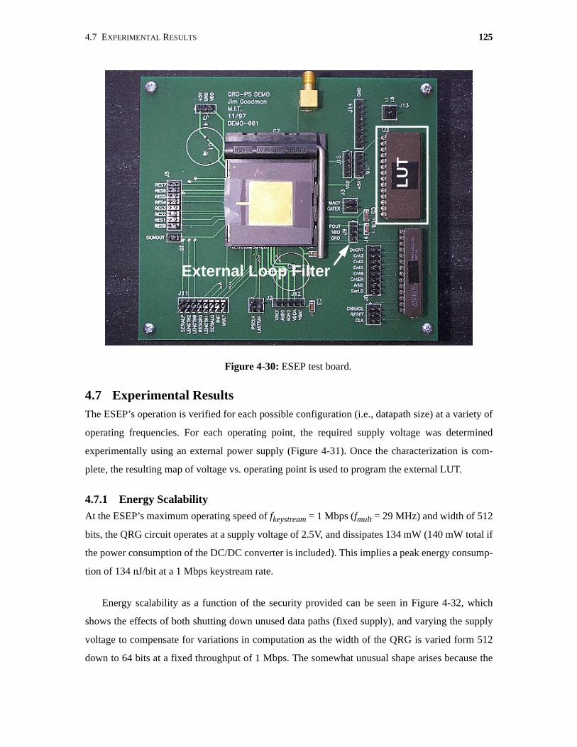
4.7 EXPERIMENTAL RESULTS 125
4.7 Experimental ResultsThe ESEP’s operation is verified for each possible configuration (i.e., datapath size) at a variety of
operating frequencies. For each operating point, the required supply voltage was determined
experimentally using an external power supply (Figure 4-31). Once the characterization is com-
plete, the resulting map of voltage vs. operating point is used to program the external LUT.
4.7.1 Energy ScalabilityAt the ESEP’s maximum operating speed of fkeystream = 1 Mbps (fmult = 29 MHz) and width of 512
bits, the QRG circuit operates at a supply voltage of 2.5V, and dissipates 134 mW (140 mW total if
the power consumption of the DC/DC converter is included). This implies a peak energy consump-
tion of 134 nJ/bit at a 1 Mbps keystream rate.
Energy scalability as a function of the security provided can be seen in Figure 4-32, which
shows the effects of both shutting down unused data paths (fixed supply), and varying the supply
voltage to compensate for variations in computation as the width of the QRG is varied form 512
down to 64 bits at a fixed throughput of 1 Mbps. The somewhat unusual shape arises because the
Figure 4-30: ESEP test board.
LU
T
External Loop Filter

126 CHAPTER 4 ENERGY SCALABLE ENCRYPTION PROCESSOR (ESEP)
operating frequency of the QRG is a non-linear function of the QRG width:
(4-9)
Figure 4-32 (a) also demonstrates the benefits of using a variable supply voltage relative to a fixed
supply; the energy reduction due to the variable supply varies between 1x at a width of 512 bits to
3.8x at a width of 64 bits. The resulting relationship between security and energy consumption is
shown in Figure 4-32 (b), where the energy consumption varies by a factor of 30 as the security is
varied across its range of possible of values.
Figure 4-33, demonstrates the energy savings that can be achieved as a function of the required
throughput when the dynamically adjustable embedded power supply is used. Note that the energy
Figure 4-31: Required QRG supply voltage as a function of throughput and security.
Throughput(Mbps)
Datapath Width(bits)
Supp
ly V
olta
ge(V
)
fmultn 2 4+⁄
n2log-------------------- fkeystream⋅=
256 384 5120
50
100
150
Ene
rgy
@ 1
Mb/
s (n
J/bi
t)
QRG Width (bits)
variablesupply
fixedsupply
12864 192 320 448
25
75
125
Figure 4-32: Energy consumption of the ESEP as a function of QRG width and security.
150
100
10-10 10-5 100 1050
50
512b
448b
384b
320b256b
192b128b64b
Security (MIPS-years)
Ene
rgy
@ 1
Mb/
s (n
J/bi
t)
(a) (b)
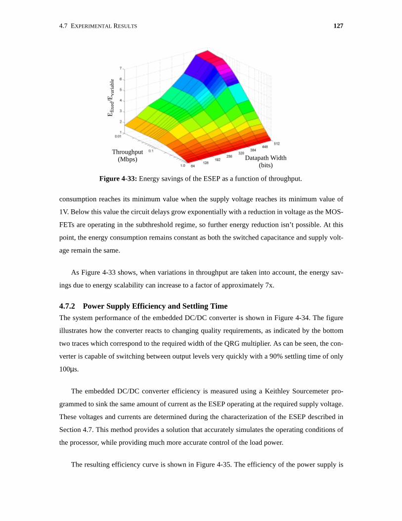
4.7 EXPERIMENTAL RESULTS 127
consumption reaches its minimum value when the supply voltage reaches its minimum value of
1V. Below this value the circuit delays grow exponentially with a reduction in voltage as the MOS-
FETs are operating in the subthreshold regime, so further energy reduction isn’t possible. At this
point, the energy consumption remains constant as both the switched capacitance and supply volt-
age remain the same.
As Figure 4-33 shows, when variations in throughput are taken into account, the energy sav-
ings due to energy scalability can increase to a factor of approximately 7x.
4.7.2 Power Supply Efficiency and Settling Time
The system performance of the embedded DC/DC converter is shown in Figure 4-34. The figure
illustrates how the converter reacts to changing quality requirements, as indicated by the bottom
two traces which correspond to the required width of the QRG multiplier. As can be seen, the con-
verter is capable of switching between output levels very quickly with a 90% settling time of only
100µs.
The embedded DC/DC converter efficiency is measured using a Keithley Sourcemeter pro-
grammed to sink the same amount of current as the ESEP operating at the required supply voltage.
These voltages and currents are determined during the characterization of the ESEP described in
Section 4.7. This method provides a solution that accurately simulates the operating conditions of
the processor, while providing much more accurate control of the load power.
The resulting efficiency curve is shown in Figure 4-35. The efficiency of the power supply is
Figure 4-33: Energy savings of the ESEP as a function of throughput.
Efi
xed/
Eva
riab
le
Throughput(Mbps) Datapath Width
(bits)
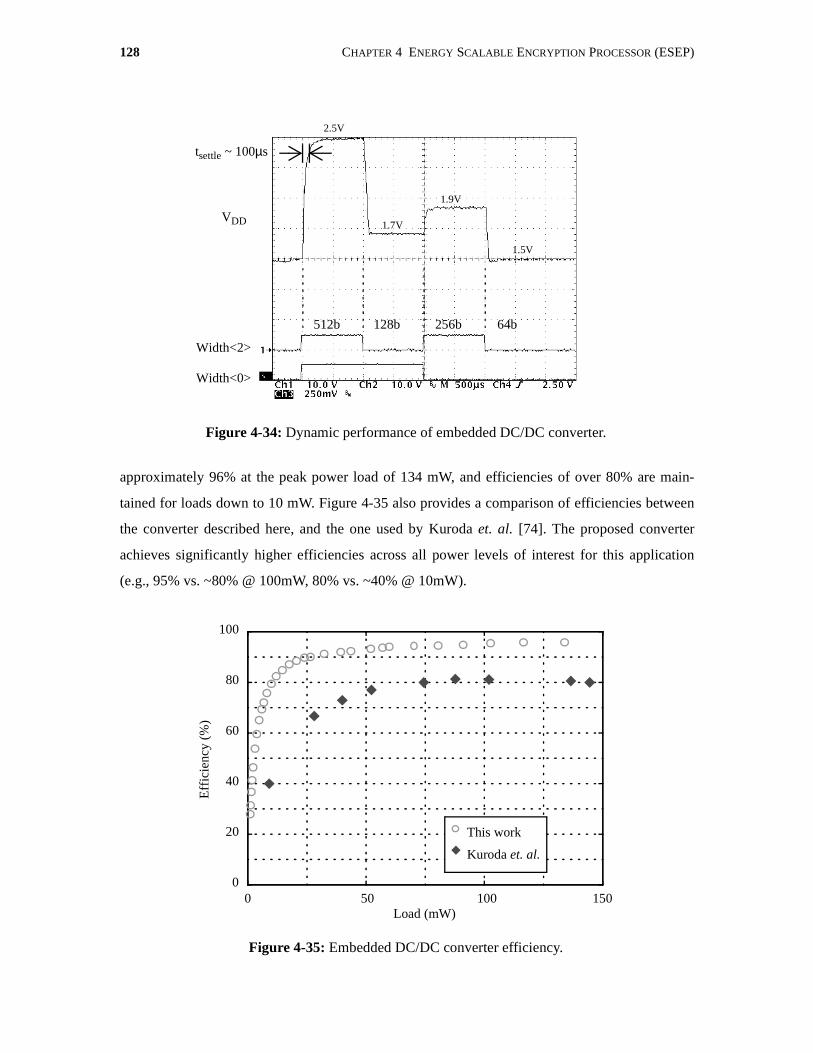
128 CHAPTER 4 ENERGY SCALABLE ENCRYPTION PROCESSOR (ESEP)
approximately 96% at the peak power load of 134 mW, and efficiencies of over 80% are main-
tained for loads down to 10 mW. Figure 4-35 also provides a comparison of efficiencies between
the converter described here, and the one used by Kuroda et. al. [74]. The proposed converter
achieves significantly higher efficiencies across all power levels of interest for this application
(e.g., 95% vs. ~80% @ 100mW, 80% vs. ~40% @ 10mW).
Figure 4-34: Dynamic performance of embedded DC/DC converter.
Width<2>
Width<0>
VDD
1.5V
1.9V
1.7V
512b 64b256b128b
2.5V
tsettle ~ 100µs
Figure 4-35: Embedded DC/DC converter efficiency.
Load (mW)
Eff
icie
ncy
(%)
0 50 100 1500
20
40
60
80
100
This work
Kuroda et. al.
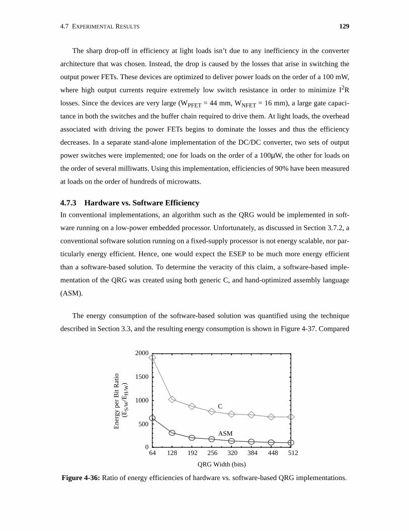
4.7 EXPERIMENTAL RESULTS 129
The sharp drop-off in efficiency at light loads isn’t due to any inefficiency in the converter
architecture that was chosen. Instead, the drop is caused by the losses that arise in switching the
output power FETs. These devices are optimized to deliver power loads on the order of a 100 mW,
where high output currents require extremely low switch resistance in order to minimize I2R
losses. Since the devices are very large (WPFET = 44 mm, WNFET = 16 mm), a large gate capaci-
tance in both the switches and the buffer chain required to drive them. At light loads, the overhead
associated with driving the power FETs begins to dominate the losses and thus the efficiency
decreases. In a separate stand-alone implementation of the DC/DC converter, two sets of output
power switches were implemented; one for loads on the order of a 100µW, the other for loads on
the order of several milliwatts. Using this implementation, efficiencies of 90% have been measured
at loads on the order of hundreds of microwatts.
4.7.3 Hardware vs. Software Efficiency
In conventional implementations, an algorithm such as the QRG would be implemented in soft-
ware running on a low-power embedded processor. Unfortunately, as discussed in Section 3.7.2, a
conventional software solution running on a fixed-supply processor is not energy scalable, nor par-
ticularly energy efficient. Hence, one would expect the ESEP to be much more energy efficient
than a software-based solution. To determine the veracity of this claim, a software-based imple-
mentation of the QRG was created using both generic C, and hand-optimized assembly language
(ASM).
The energy consumption of the software-based solution was quantified using the technique
described in Section 3.3, and the resulting energy consumption is shown in Figure 4-37. Compared
Figure 4-36: Ratio of energy efficiencies of hardware vs. software-based QRG implementations.
64 128 192 256 320 384 448 5120
500
1000
1500
2000
Ene
rgy
per
Bit
Rat
io
QRG Width (bits)
(ES
/W/E
H/W
)
C
ASM

130 CHAPTER 4 ENERGY SCALABLE ENCRYPTION PROCESSOR (ESEP)
to the hardware-based ESEP, the software implementation is two to three orders of magnitude
more energy inefficient (Figure 4-36). Note that this comparison is performed under conditions
that benefit the software-based solutions, with the throughput set to the peak rate possible via soft-
ware (25 Kbps and 125 Kbps for the C and ASM implementations respectively). Were the compar-
ison made at a lower throughput, the ESEP could reduce its supply voltage, and hence its energy
consumption. Since the software based solution is tied to a fixed supply voltage, it’s energy would
not decrease. In fact, the energy consumption will actually increase when the rate is reduced suffi-
ciently low as the StrongARM SA-1100 has significant leakage currents which lead to non-zero
power consumption during idle periods that must be accounted for in the total energy consumption
of a given operation.
4.8 Summary of ContributionsThis chapter saw the introduction of the notion of energy scalable computing in which the time-
varying quality and throughput requirements of the data stream are exploited by an architecture in
order to minimize the average energy consumption of the system. Energy scalable computing is
most useful where data rates and quality requirements vary greatly. In terms of cryptographic
applications this occurs in the data encryption function which ties symmetric key ciphers to the
data stream.
An energy scalable architecture for providing data encryption was described and implemented
in the form of the Energy Scalable Encryption Processor (ESEP). The ESEP features the ability to
dynamically adjust both the level of security that is being provided, and the supply voltage at
Figure 4-37: Energy consumption of software-based QRG implementation.
QRG Width (bits)
64 128 192 256 320 384 448 5120
2
4
6
8
10
12
14
Ene
rgy
per
Bit
(mJ/
bit)
ASM
C

4.8 SUMMARY OF CONTRIBUTIONS 131
which the processor is operating through the use of a partitioned datapath and embedded program-
mable high efficiency variable-output DC/DC converter.
The ESEP validates the thesis of Energy Scalability by demonstrating that energy consump-
tion can be reduced by a factor of 7 as a function of throughput, and 30 as a function of security. A
comparison of the ESEP to both a conventional and optimized software-based solution demon-
strates over two orders of magnitude improvement in energy efficiency for the energy scalable
implementation.
The embedded DC/DC converter used within the ESEP demonstrates the benefits of utilizing a
hybrid delay-line and PLL-based fixed-frequency PWM architecture for doing low load power
conversion. The converter achieves efficiencies over 90% at loads on the order of 10’s of mW, and
is capable of achieving similar efficiencies at loads on the order of 10’s of µW as well. Compared
to other published power converters, our implementation is significantly more efficient under all
operating conditions.

132 CHAPTER 4 ENERGY SCALABLE ENCRYPTION PROCESSOR (ESEP)
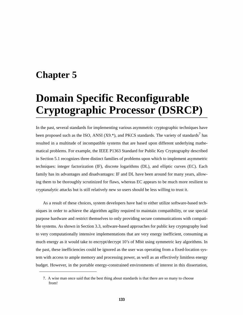
133133133
Chapter 5
Domain Specific Reconfigurable Cryptographic Processor (DSRCP)In the past, several standards for implementing various asymmetric cryptographic techniques have
been proposed such as the ISO, ANSI (X9.*), and PKCS standards. The variety of standards7 has
resulted in a multitude of incompatible systems that are based upon different underlying mathe-
matical problems. For example, the IEEE P1363 Standard for Public Key Cryptography described
in Section 5.1 recognizes three distinct families of problems upon which to implement asymmetric
techniques: integer factorization (IF), discrete logarithms (DL), and elliptic curves (EC). Each
family has its advantages and disadvantages: IF and DL have been around for many years, allow-
ing them to be thoroughly scrutinized for flaws, whereas EC appears to be much more resilient to
cryptanalytic attacks but is still relatively new so users should be less willing to trust it.
As a result of these choices, system developers have had to either utilize software-based tech-
niques in order to achieve the algorithm agility required to maintain compatibility, or use special
purpose hardware and restrict themselves to only providing secure communications with compati-
ble systems. As shown in Section 3.3, software-based approaches for public key cryptography lead
to very computationally intensive implementations that are very energy inefficient, consuming as
much energy as it would take to encrypt/decrypt 10’s of Mbit using symmetric key algorithms. In
the past, these inefficiencies could be ignored as the user was operating from a fixed-location sys-
tem with access to ample memory and processing power, as well as an effectively limitless energy
budget. However, in the portable energy-constrained environments of interest in this dissertation,
7. A wise man once said that the best thing about standards is that there are so many to choose from!

134 CHAPTER 5 DOMAIN SPECIFIC RECONFIGURABLE CRYPTOGRAPHIC PROCESSOR (DSRCP)
these inefficiencies require us to re-evaluate the use of a software-based implementation. The alter-
native hardware-based implementations, while being very energy and computationally efficient,
are very inflexible and don’t satisfy the compatibility constraints that are necessary to increase the
utility of portable computing devices.
In this chapter a compromise between these two extremes is proposed by taking advantage of
the fact that the range of operations necessary to implement the required public key cryptographic
algorithms is small enough that domain specific reconfigurable hardware can be developed which
delivers the required algorithm agility. Furthermore, this is done in an energy-efficient manner that
enables operation in the portable, energy-constrained environments where algorithm agility is
required most of all. The resulting implementation is known as the Domain Specific Reconfig-
urable Cryptographic Processor (DSRCP).
5.1 IEEE Public Key Cryptography Standard (P1363)In 1977, the U.S. Government proposed a new standard for symmetric key cryptography known as
the Data Encryption Standard (DES) [43]. By introducing a single standard, the Government pro-
vided industry with a reference implementation which has since been adopted extensively, and is
still in use today, almost twenty five years later [44]. In the last few years, the search for a replace-
ment to DES has begun in the form of the Advanced Encryption Standard (AES). The develop-
ment of AES will ensure standardization for secret key cryptography for years to come.
Unfortunately, no such effort was made for wide-ranging standardization of asymmetric key cryp-
tography until the recent IEEE P1363 Standard for Public Key Cryptography [56].
P1363 standardizes the use of various public key cryptographic algorithms in order to provide
three basic types of cryptographic functions: key agreement, digital signatures, and public key
encryption. These functions were chosen as they represent the most useful functions of public key
cryptography:
• Key agreement functions allow two parties to establish a set of secret keys in the pres-ence of adversaries. These keys can then be used by much more efficient secret keyalgorithms to encrypt/decrypt data transmissions between the two parties.
• Digital signatures are used to “sign” digital data in much the same way that a person’shandwritten signature is used. The digital signature provides irrefutable proof that agiven user generated a particular piece of digital data, and that the data has not beenmodified.
• Public key encryption is simply the application of an asymmetric algorithm to encodedata in those cases where symmetric key encryption is not feasible.
5.1 IEEE PUBLIC KEY CRYPTOGRAPHY STANDARD (P1363) 135
In addition, P1363 also defines three separate hard number theoretic problems upon which to
build the aforementioned cryptographic functions: integer factorization, discrete logarithms, and
discrete logarithms over elliptic curves. The following sections describe each of these problems in
terms of where they came from, how they are used, how they derive their security, and how to
quantify their security based on the implementation parameters.
5.1.1 Discrete Logarithm (DL)
The problem of finding discrete logarithms (DL) over large finite fields was first proposed by Dif-
fie and Hellman [36], and was the first public example of an asymmetric cryptographic algorithm8.
The security of DL-based schemes relies on the difficulty of computing logarithms within a finite
cyclic multiplicative group (e.g., Zp* or GF(2p)* where p is a large prime). The algorithm exploits
the fact that given a generator g of the group G, it is easy to compute ga ∈ G for some random inte-
ger a, but given ga it is computationally infeasible (for groups of sufficiently large order) to com-
pute a. As such, two users (such as our old friends Alice and Bob) can establish a secret using the
following basic protocol:
• Alice and Bob agree on a generator g and group G, neither of which needs to be keptsecret
• Alice and Bob generate random values a and b respectively which they keep secret
• Alice sends ga to Bob, and Bob sends gb to Alice.
• Alice computes (gb)a = gab, and Bob computes (ga)b = gab
At the completion of the above protocol Alice and Bob will share the secret value gab, and an
eavesdropper, Eve, will only have learned the values ga and gb. Assuming that computing discrete
logarithms over G is infeasible, then the eavesdropper is only able to compute ga+b. Hence, A and
B have managed to share a secret over an unprotected channel. Other techniques based on discrete
logarithms have also been proposed (e.g., El Gamal encryption and signature schemes [41]), all of
which rely on performing computations over a finite field such as Zp* or GF(2p).
P1363 describes DL-based key agreement schemes based upon the work of Diffie-Hellman
[36] and Menezes-Qu-Vanstone [83], as well as digital schemes based upon the work of Nyberg-
Rueppel [90], and the Digital Signature Algorithm [47]. The basic cryptographic primitive used by
these schemes is exponentiation within GF(q)*, where q is either a large prime or 2m. Additional
8. Originally it was thought that it was the first demonstration of public key cryptography period, but recent evidence [42] has shown that the technique had been discovered by the military sev-eral years earlier.
136 CHAPTER 5 DOMAIN SPECIFIC RECONFIGURABLE CRYPTOGRAPHIC PROCESSOR (DSRCP)
field operations such as multiplication, addition/subtraction, and inversion are also utilized.
The security of DL-based cryptography is based on the difficulty of computing discrete loga-
rithms over the given field (i.e., Zp* or GF(2m)). The most efficient algorithms for computing dis-
crete logarithms over Zp* utilize a method known as Index Calculus [2] in order to compute a
discrete logarithm in time that is proportional to Lp[v, c], which is defined as follows:
(5-1)
Both c, a constant factor, and v, a non-negative value less than 1, are determined by the discrete
logarithm algorithm that is used. For Zp*, the current state-of-the-art algorithms run in Lp[1/3,
~1.923], and for GF(2m) Coppersmith [30] developed an optimized algorithm whose running time
is on the order of .
5.1.2 Integer Factorization (IF)
Integer factorization was originally proposed as a means of implementing public key cryptography
in 1978 with the introduction of Rivest, Shamir, and Adleman’s well-known RSA algorithm [107].
IF-based algorithms utilize the cyclic multiplicative subgroup formed by the integers modulo-N,
where N is a large n-bit composite integer formed by the product of two randomly generated n/2-
bit primes (typically denoted as p and q). The RSA algorithm utilizes the fact that the order of the
cyclic multiplicative subgroup of Zn* is φ(n) = (p-1)(q-1), and thus for any , the following
relation holds:
(5-2)
One then chooses two values e and d that satisfy the relation:
(5-3)
The value e is called the public exponent and along with n forms the public key. The value d is
called the secret exponent and forms the private key. With these values one can encrypt a message,
x < n, using modular exponentiation with e, and decrypt the result using modular exponentiation
with d. The encrypt/decrypt operation is illustrated in EQ 5-4.
(5-4)
Obviously, if one could compute the factorization of n, then one could compute φ(n) and find d
Lp v c,[ ] ec plog( )v
ploglog( )1 v–
=
L2
m 1 3 <1.587,⁄[ ]
a Zn*∈
aφ n( )
1 mod n=
e d⋅ 1 mod φ n( )=
xe( )
dmod n x
e d⋅ mod n
xa φ n( ) 1+⋅
mod n
xφ n( )( )
ax
1 mod n⋅
1( )a x mod n⋅x mod n
=
=
=
=
=
5.1 IEEE PUBLIC KEY CRYPTOGRAPHY STANDARD (P1363) 137
using the fact that d = e-1 mod φ(n). Hence, RSA is no more difficult to break than the problem of
integer factorization. Note that the encryption and decryption operations commute, a feature that is
used extensively for digital signature generation.
P1363 describes IF-based digital signature schemes based upon the work of Rivest-Shamir-
Adleman [107], Rabin [103], and Miller’s extension of Rabin’s work [134]. Public key encryption
schemes based upon RSA are also described. The basic cryptographic primitive used by the IF-
based schemes is modular exponentiation, with additional modular arithmetic operations such as
addition/subtraction, multiplication, and inversion being required as well.
Schemes based upon IF exploit the fact that factoring large composite integers (e.g., 512+ bits
long) into their constituent prime factors is a very difficult problem. The effort that is required to
factor very large numbers is closely related to that of computing discrete logarithms over fields of
comparable size. In fact, the complexity of factoring a given modulus N using state-of-the-art fac-
toring algorithms such as the General Number Field Sieve [76] (GNFS) is stated in the same man-
ner as computing discrete logarithms: LN[v, c]. This similarity arises due to the fact that both
factoring and discrete logarithms utilize the aforementioned Index Calculus methods, hence it
should come as no surprise that they have comparable running times. The fastest general purpose
factoring algorithm, the GNFS, achieves a running time on order LN[1/3, ~1.923].
5.1.3 Elliptic Curve Discrete Logarithm (ECDL)The elliptic curve discrete logarithm problem is closely related to the discrete logarithm problem
over multiplicative groups, except now the group is the set of points found on an elliptic curve over
the field GF(q), and the group operation is addition as opposed to multiplication. Hence, the ellip-
tic curve discrete logarithm problem relies on the difficulty of determining the integer n, given
only the curve E and the points P and nP.
All of the ECDL-based schemes described in P1363 are analogs of the DL-based schemes
described in Section 5.1.1, with exponentiation over multiplicative groups replaced by point multi-
plication over the additive group formed by the points on an elliptic curve over GF(q), where q is
either prime or 2m.
The primary advantage of using elliptic curves is that the powerful Index Calculus method
appears to be unusable for computing discrete logarithms over elliptic curves. Without Index Cal-
culus, the best method of computing discrete logarithms is the Pollard-Rho algorithm [98] and its
138 CHAPTER 5 DOMAIN SPECIFIC RECONFIGURABLE CRYPTOGRAPHIC PROCESSOR (DSRCP)
parallelized extension [92], which compute discrete logarithms in time, where n is the
order of the point P being multiplied. For a properly chosen curve and point, the value n will be
close to the order of the field upon which the curve is constructed (i.e., GF(q)). Hence, in terms of
the number of bits used to represent the field, the complexity of computing discrete
logarithms over an elliptic curve is fully exponential, O(2m/2), a substantial improvement over the
sub-exponential complexity of the IF and DL problems. Hence, elliptic curve cryptography
appears to be much more secure than its IF and DL-based counterparts, a fact that is evident by its
much shorter key sizes.
5.2 Programmable Logic and Domain Specific ReconfigurabilityIn conventional reconfigurable applications such as Field Programmable Gate Arrays (FPGAs),
the architectural goals of the device are to provide a large number of very small, yet powerful pro-
grammable logic cells, and very flexible programmable interconnect to connect these cells
together. This approach has proven very successful in terms of both performance and flexibility,
with FPGA-based implementations being used extensively in industrial applications where moder-
ately high levels of performance are required and the high costs and lengthy design cycles of semi
or full custom integrated circuits cannot be justified.
In the past, the use of programmable logic in cryptography has been limited primarily to
implementations of symmetric key algorithms such as DES (e.g., [135], [105], [48], [62], and
[39]). Unfortunately, asymmetric key algorithms were largely ignored as the high gate counts
required for efficient implementation were not available in a single device. The latest advances in
programmable logic have addressed and alleviated this constraint by delivering devices with
usable gate counts on the order of several hundred thousand. As a result, there has been great inter-
est in implementing asymmetric algorithms using programmable logic ([93], [20], and [109]), both
because of the increased throughput that it yields relative to conventional software-based solu-
tions, and the flexibility it provides by allowing one to reprogram it on the fly to implement a vari-
ety of algorithms.
Until recently, these programmable implementations have been optimized to leverage a maxi-
mum amount of flexibility while maintaining a minimum level of performance. Issues such as
power consumption have largely been ignored in all cases except those where the sheer size of the
device warrants some form of power management in order to prevent failure due to thermal effects.
This issue is now being addressed with the latest families of programmable logic devices such as
O n( )
m q2log=

5.3 INSTRUCTION SET DEFINITION/ARCHITECTURE 139
Xilinx’s Virtex [136] and Altera’s APEX 20K [9], which utilize low power modes and architec-
tural features to reduce power dissipation.
Despite these recent advances, the overhead associated with making such a general purpose
computing device will ultimately limit its energy efficiency, and hence its utility in energy-con-
strained environments. To illustrate this fact consider the space of all possible functions. A conven-
tional reconfigurable logic device attempts to cover as much of this space as possible given its
architectural constraints in terms of technology, logic resources, and routing resources. This results
in a considerable amount of overhead that isn’t necessary given a specific subset of functions.
Kusse [75] attempted to quantify this overhead by breaking down the energy consumption of a
conventional FPGA by its architectural components (Figure 5-1). Their analysis reveals that only
1/20th of the total energy is being used to perform useful computation.
The DSRCP differs from conventional reconfigurable implementations in that its reconfig-
urability is limited to the subset of functions, called a domain, required for asymmetric cryptogra-
phy. This domain requires only a small set of configurations for performing the required operations
over all possible problem families as defined by IEEE P1363. As a result, the reconfiguration over-
head is much smaller in terms of performance, energy efficiency, and reconfiguration time make
the DSRCP feasible for algorithm-agile asymmetric cryptography in energy constrained environ-
ments. In addition, from an architectural standpoint the DSRCP focuses on minimizing the domi-
nant interconnect component of Figure 5-1 by utilizing an interconnect-centric architecture that
attempts to minimize global interconnect by exploiting a bit-sliced implementation with pre-domi-
nantly local interconnections.
5.3 Instruction Set Definition/ArchitectureThe instruction set definition of the DSRCP is dictated by the IEEE P1363 description document.
For each primitive listed in the standard, a list of the required arithmetic functions is tabulated in
order to determine the required ISA of the processor. Note that certain primitives also require such
Interconnect (65%)Global Clock (21%)
Logic (5%)I/O (9%)
Figure 5-1: Energy consumption breakdown of XILINX XC4003A [75].
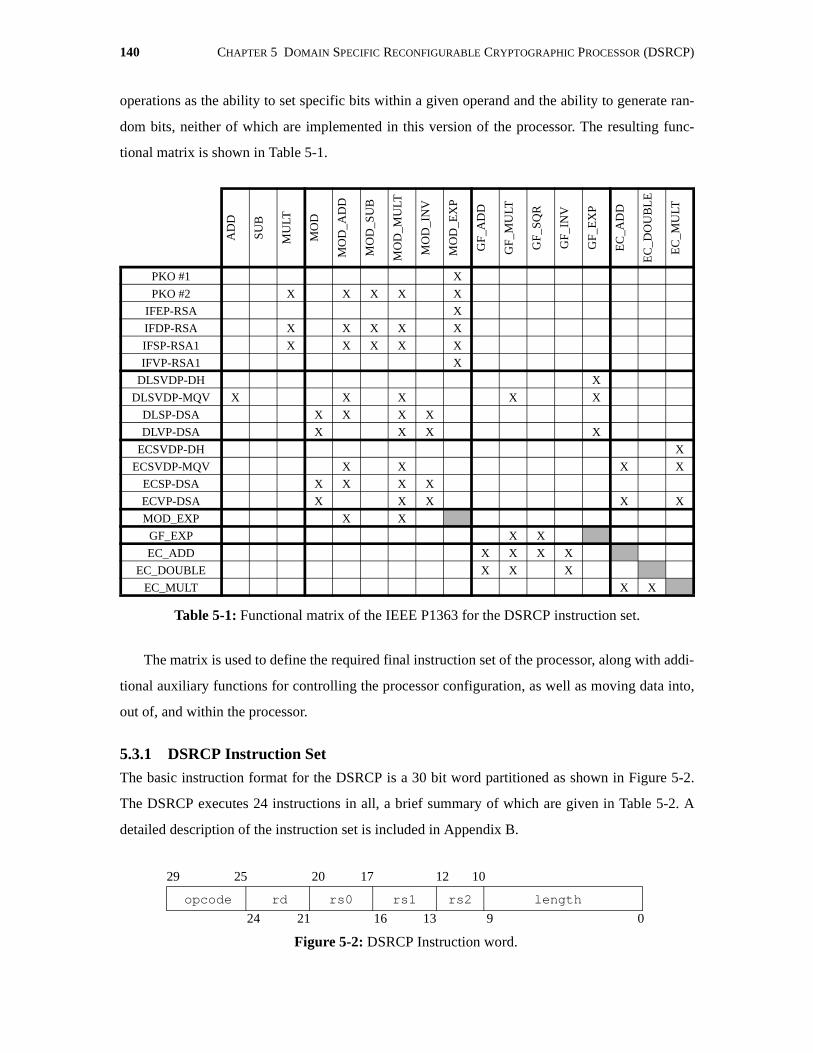
140 CHAPTER 5 DOMAIN SPECIFIC RECONFIGURABLE CRYPTOGRAPHIC PROCESSOR (DSRCP)
operations as the ability to set specific bits within a given operand and the ability to generate ran-
dom bits, neither of which are implemented in this version of the processor. The resulting func-
tional matrix is shown in Table 5-1.
The matrix is used to define the required final instruction set of the processor, along with addi-
tional auxiliary functions for controlling the processor configuration, as well as moving data into,
out of, and within the processor.
5.3.1 DSRCP Instruction Set
The basic instruction format for the DSRCP is a 30 bit word partitioned as shown in Figure 5-2.
The DSRCP executes 24 instructions in all, a brief summary of which are given in Table 5-2. A
detailed description of the instruction set is included in Appendix B.
AD
D
SU
B
MU
LT
MO
D
MO
D_A
DD
MO
D_S
UB
MO
D_M
ULT
MO
D_I
NV
MO
D_E
XP
GF
_AD
D
GF_
MU
LT
GF_
SQR
GF_
INV
GF_
EX
P
EC
_AD
D
EC
_DO
UB
LE
EC
_MU
LT
PKO #1 X
PKO #2 X X X X X
IFEP-RSA X
IFDP-RSA X X X X X
IFSP-RSA1 X X X X X
IFVP-RSA1 X
DLSVDP-DH X
DLSVDP-MQV X X X X X
DLSP-DSA X X X X
DLVP-DSA X X X X
ECSVDP-DH X
ECSVDP-MQV X X X X
ECSP-DSA X X X X
ECVP-DSA X X X X X
MOD_EXP X X
GF_EXP X X
EC_ADD X X X X
EC_DOUBLE X X X
EC_MULT X X
Table 5-1: Functional matrix of the IEEE P1363 for the DSRCP instruction set.
Figure 5-2: DSRCP Instruction word.
29 25
24 21
20 17
16 13
12 10
9 0
opcode rd rs0 rs1 rs2 length
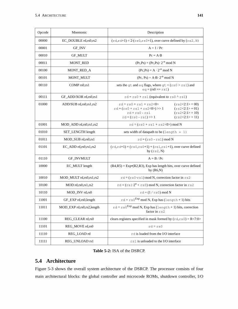
5.4 ARCHITECTURE 141
5.4 ArchitectureFigure 5-3 shows the overall system architecture of the DSRCP. The processor consists of four
main architectural blocks: the global controller and microcode ROMs, shutdown controller, I/O
Opcode Mnemonic Description
00000 EC_DOUBLE rd,rs0,rs2 (rd,rd+1) = 2·(rs0,rs0+1), over curve defined by (rs2,N)
00001 GF_INV A = 1 / Pc
00010 GF_MULT Pc = A·B
00011 MONT_RED (Pc,Ps) = (Pc,Ps)· 2-n mod N
00100 MONT_RED_A (Pc,Ps) = A · 2-n mod N
00101 MONT_MULT (Pc, Ps) = A·B· 2-n mod N
00110 COMP rs0,rs1 sets the gt and eq flags, where gt = (rs0 > rs1) andeq = (rs0 == rs1)
00111 GF_ADD/XOR rd,rs0,rs1 rd = rs0 + rs1 (equivalent to rs0 ^ rs1)
01000 ADD/SUB rd,rs0,rs1,rs2 rd = rs0 + rs1 + rs2<0> rd = (rs0 + rs1 + rs2<0>) >> 1
rd = rs0 - rs1 rd = (rs0 - rs1) >> 1
(rs2<2:1> = 00)(rs2<2:1> = 01)(rs2<2:1> = 10)(rs2<2:1> = 11)
01001 MOD_ADD rd,rs0,rs1,rs2 rd = (rs0 + rs1 + rs2<0>) mod N
01010 SET_LENGTH length sets width of datapath to be (length + 1)
01011 MOD_SUB rd,rs0,rs1 rd = (rs0 - rs1) mod N
01101 EC_ADD rd,rs0,rs1,rs2 (rd,rd+1) = (rs0,rs0+1) + (rs1,rs1+1), over curve defined by (rs2, N)
01110 GF_INVMULT A = B / Pc
10000 EC_MULT length (R4,R5) = Exp•(R2,R3), Exp has length bits, over curve defined by (R6,N)
10010 MOD_MULT rd,rs0,rs1,rs2 rd = (rs0·rs1) mod N, correction factor in rs2
10100 MOD rd,rs0,rs1,rs2 rd = (rs1·2n + rs0) mod N, correction factor in rs2
10110 MOD_INV rd,rs0 rd = (1 / rs0) mod N
11001 GF_EXP rd,rs0,length rd = rs0Exp mod N, Exp has (length + 1) bits
11011 MOD_EXP rd,rs0,rs2,length rd = rs0Exp mod N, Exp has (length + 1) bits, correctionfactor in rs2
11100 REG_CLEAR rd,rs0 clears registers specified in mask formed by (rd,rs0) = R<7:0>
11101 REG_MOVE rd,rs0 rd = rs0
11110 REG_LOAD rd rd is loaded from the I/O interface
11111 REG_UNLOAD rs1 rs1 is unloaded to the I/O interface
Table 5-2: ISA of the DSRCP.
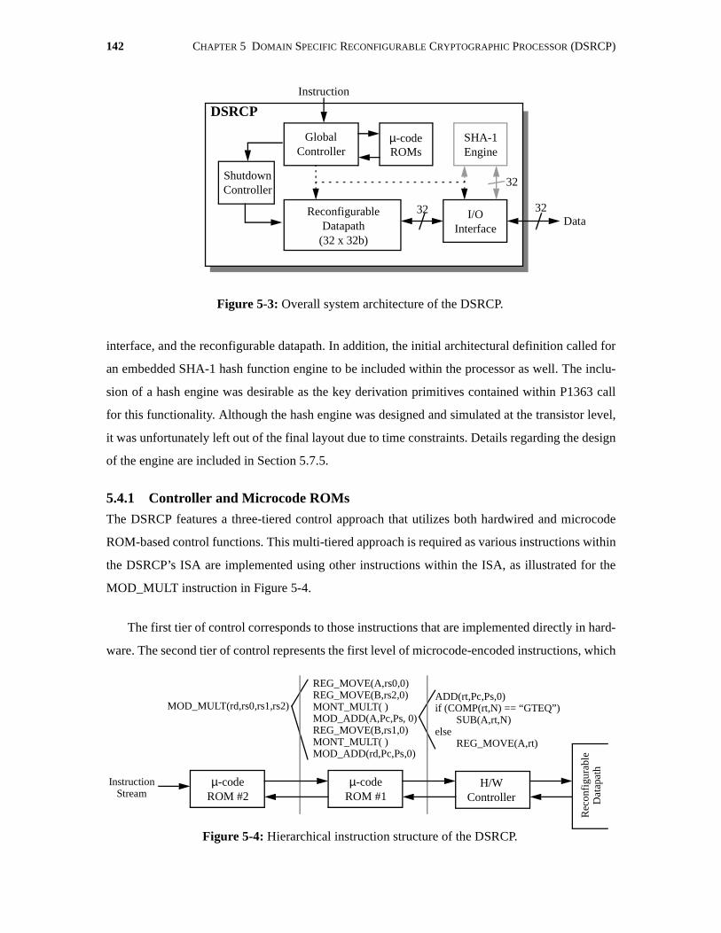
142 CHAPTER 5 DOMAIN SPECIFIC RECONFIGURABLE CRYPTOGRAPHIC PROCESSOR (DSRCP)
interface, and the reconfigurable datapath. In addition, the initial architectural definition called for
an embedded SHA-1 hash function engine to be included within the processor as well. The inclu-
sion of a hash engine was desirable as the key derivation primitives contained within P1363 call
for this functionality. Although the hash engine was designed and simulated at the transistor level,
it was unfortunately left out of the final layout due to time constraints. Details regarding the design
of the engine are included in Section 5.7.5.
5.4.1 Controller and Microcode ROMs
The DSRCP features a three-tiered control approach that utilizes both hardwired and microcode
ROM-based control functions. This multi-tiered approach is required as various instructions within
the DSRCP’s ISA are implemented using other instructions within the ISA, as illustrated for the
MOD_MULT instruction in Figure 5-4.
The first tier of control corresponds to those instructions that are implemented directly in hard-
ware. The second tier of control represents the first level of microcode-encoded instructions, which
Figure 5-3: Overall system architecture of the DSRCP.
GlobalController
µ-codeROMs
SHA-1Engine
ReconfigurableDatapath
(32 x 32b)
I/OInterface
Instruction
32
3232Data
DSRCP
ShutdownController
Figure 5-4: Hierarchical instruction structure of the DSRCP.
MOD_MULT(rd,rs0,rs1,rs2)
REG_MOVE(A,rs0,0)REG_MOVE(B,rs2,0)MONT_MULT( )MOD_ADD(A,Pc,Ps, 0)REG_MOVE(B,rs1,0)MONT_MULT( )MOD_ADD(rd,Pc,Ps,0)
ADD(rt,Pc,Ps,0)if (COMP(rt,N) == “GTEQ”)
SUB(A,rt,N)else
REG_MOVE(A,rt)
µ-codeROM #2
µ-codeROM #1
H/WController
Rec
onfi
gura
ble
Dat
apat
h
InstructionStream
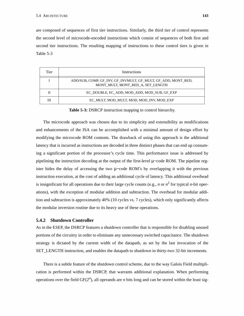
5.4 ARCHITECTURE 143
are composed of sequences of first tier instructions. Similarly, the third tier of control represents
the second level of microcode-encoded instructions which consist of sequences of both first and
second tier instructions. The resulting mapping of instructions to these control tiers is given in
Table 5-3
The microcode approach was chosen due to its simplicity and extensibility as modifications
and enhancements of the ISA can be accomplished with a minimal amount of design effort by
modifying the microcode ROM contents. The drawback of using this approach is the additional
latency that is incurred as instructions are decoded in three distinct phases that can end up consum-
ing a significant portion of the processor’s cycle time. This performance issue is addressed by
pipelining the instruction decoding at the output of the first-level µ−code ROM. The pipeline reg-
ister hides the delay of accessing the two µ−code ROM’s by overlapping it with the previous
instruction execution, at the cost of adding an additional cycle of latency. This additional overhead
is insignificant for all operations due to their large cycle counts (e.g., n or n2 for typical n-bit oper-
ations), with the exception of modular addition and subtraction. The overhead for modular addi-
tion and subtraction is approximately 40% (10 cycles vs. 7 cycles), which only significantly affects
the modular inversion routine due to its heavy use of these operations.
5.4.2 Shutdown Controller
As in the ESEP, the DSRCP features a shutdown controller that is responsible for disabling unused
portions of the circuitry in order to eliminate any unnecessary switched capacitance. The shutdown
strategy is dictated by the current width of the datapath, as set by the last invocation of the
SET_LENGTH instruction, and enables the datapath to shutdown in thirty-two 32-bit increments.
There is a subtle feature of the shutdown control scheme, due to the way Galois Field multipli-
cation is performed within the DSRCP, that warrants additional explanation. When performing
operations over the field GF(2n), all operands are n bits long and can be stored within the least sig-
Tier Instructions
I ADD/SUB, COMP, GF_INV, GF_INVMULT, GF_MULT, GF_ADD, MONT_RED, MONT_MULT, MONT_RED_A, SET_LENGTH
II EC_DOUBLE, EC_ADD, MOD_ADD, MOD_SUB, GF_EXP
III EC_MULT, MOD_MULT, MOD, MOD_INV, MOD_EXP
Table 5-3: DSRCP instruction mapping to control hierarchy.
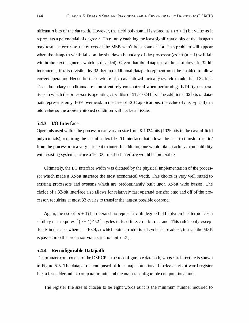
144 CHAPTER 5 DOMAIN SPECIFIC RECONFIGURABLE CRYPTOGRAPHIC PROCESSOR (DSRCP)
nificant n bits of the datapath. However, the field polynomial is stored as a (n + 1) bit value as it
represents a polynomial of degree n. Thus, only enabling the least significant n bits of the datapath
may result in errors as the effects of the MSB won’t be accounted for. This problem will appear
when the datapath width falls on the shutdown boundary of the processor (as bit (n + 1) will fall
within the next segment, which is disabled). Given that the datapath can be shut down in 32 bit
increments, if n is divisible by 32 then an additional datapath segment must be enabled to allow
correct operation. Hence for these widths, the datapath will actually switch an additional 32 bits.
These boundary conditions are almost entirely encountered when performing IF/DL type opera-
tions in which the processor is operating at widths of 512-1024 bits. The additional 32 bits of data-
path represents only 3-6% overhead. In the case of ECC applications, the value of n is typically an
odd value so the aforementioned condition will not be an issue.
5.4.3 I/O Interface
Operands used within the processor can vary in size from 8-1024 bits (1025 bits in the case of field
polynomials), requiring the use of a flexible I/O interface that allows the user to transfer data to/
from the processor in a very efficient manner. In addition, one would like to achieve compatibility
with existing systems, hence a 16, 32, or 64-bit interface would be preferable.
Ultimately, the I/O interface width was dictated by the physical implementation of the proces-
sor which made a 32-bit interface the most economical width. This choice is very well suited to
existing processors and systems which are predominantly built upon 32-bit wide busses. The
choice of a 32-bit interface also allows for relatively fast operand transfer onto and off of the pro-
cessor, requiring at most 32 cycles to transfer the largest possible operand.
Again, the use of (n + 1) bit operands to represent n-th degree field polynomials introduces a
subtlety that requires cycles to load in each n-bit operand. This rule’s only excep-
tion is in the case where n = 1024, at which point an additional cycle is not added; instead the MSB
is passed into the processor via instruction bit rs22.
5.4.4 Reconfigurable Datapath
The primary component of the DSRCP is the reconfigurable datapath, whose architecture is shown
in Figure 5-5. The datapath is composed of four major functional blocks: an eight word register
file, a fast adder unit, a comparator unit, and the main reconfigurable computational unit.
The register file size is chosen to be eight words as it is the minimum number required to
n 1+( ) 32⁄
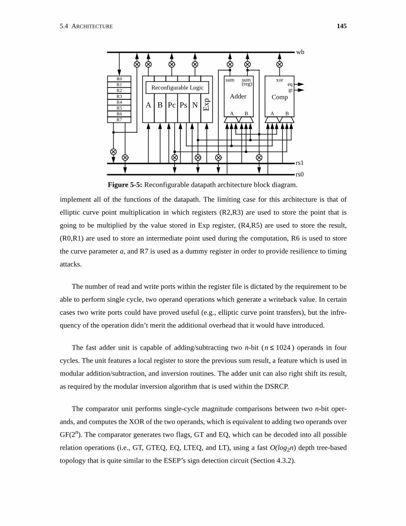
5.4 ARCHITECTURE 145
implement all of the functions of the datapath. The limiting case for this architecture is that of
elliptic curve point multiplication in which registers (R2,R3) are used to store the point that is
going to be multiplied by the value stored in Exp register, (R4,R5) are used to store the result,
(R0,R1) are used to store an intermediate point used during the computation, R6 is used to store
the curve parameter a, and R7 is used as a dummy register in order to provide resilience to timing
attacks.
The number of read and write ports within the register file is dictated by the requirement to be
able to perform single cycle, two operand operations which generate a writeback value. In certain
cases two write ports could have proved useful (e.g., elliptic curve point transfers), but the infre-
quency of the operation didn’t merit the additional overhead that it would have introduced.
The fast adder unit is capable of adding/subtracting two n-bit ( ) operands in four
cycles. The unit features a local register to store the previous sum result, a feature which is used in
modular addition/subtraction, and inversion routines. The adder unit can also right shift its result,
as required by the modular inversion algorithm that is used within the DSRCP.
The comparator unit performs single-cycle magnitude comparisons between two n-bit oper-
ands, and computes the XOR of the two operands, which is equivalent to adding two operands over
GF(2n). The comparator generates two flags, GT and EQ, which can be decoded into all possible
relation operations (i.e., GT, GTEQ, EQ, LTEQ, and LT), using a fast O(log2n) depth tree-based
topology that is quite similar to the ESEP’s sign detection circuit (Section 4.3.2).
Figure 5-5: Reconfigurable datapath architecture block diagram.
A B Pc Ps ExpN
Adder Comp
sum sum(reg)
xorR0R1R2R3R4R5R6R7
A BA B
wb
rs0
rs1
eqgtReconfigurable Logic
n 1024≤

146 CHAPTER 5 DOMAIN SPECIFIC RECONFIGURABLE CRYPTOGRAPHIC PROCESSOR (DSRCP)
The reconfigurable computation unit consists of six local registers (Pc, Ps, A, B, Exp, and N)
that are used to store intermediate values and operands to the reconfigurable portion of the datap-
ath, and a reconfigurable logic block that is capable of implementing all of the required datapath
operations. The Pc and Ps registers are used primarily in modular operations to store the carry-save
format partial product, and in Galois Field operations as two separate temporary values. A and B
store the input operands used in all modular and Galois Field operations. The Exp register is used
for storing either the exponent value, in the case of exponentiation operations, or the multiplier
value, in the case of elliptic curve point multiplication. The N register also serves a dual purpose;
for modular operations it is used as the modulus value, and in Galois Field operations, it stores the
field polynomial in a binary vector form (e.g., x3 + x2 + 1 is stored as [1,1,0,1]). In all relevant
operations, it’s assumed that both the Exp and N registers are pre-loaded with their required val-
ues.
Using local memory within the datapath eliminates the need to continually access the register
file every cycle, removing the associated overhead of repeated register file accesses. In addition,
several operations require four of the registers to be read, and two registers to be written on any
given cycle, requiring additional read and write ports to be added to the register file. This would in
turn increase the size of the register file, as well as its decoding complexity, thereby offsetting any
advantage that might be gained by going to a unified memory model that eliminated the local
memory.
The datapath utilizes three separate busses for distributing data between the various functional
units: the two operand busses (rs0 and rs1) and a writeback bus (wb). Not all registers and busses
are inter-connected as analysis and profiling dictated that not all connections were required. The
unnecessary connections were removed in order to minimize the capacitive load on the busses. rs0
is also used as a secondary writeback bus to enable values within the datapath to be transferred to
other registers within the datapath.
As described in Section 5.4.2, all functional units within the datapath can be shutdown in 32
bit increments to minimize unnecessary switched capacitance when the processor is operating at a
reduced width.
5.5 Algorithm ImplementationThe DSRCP implements a wide range of functions, most of which are composed of other func-

5.5 ALGORITHM IMPLEMENTATION 147
tions executed by the processor. Given this nested construction, some consideration must be made
as to how the various operations are implemented algorithmically in terms of the DSRCP’s instruc-
tion set.
In this section we address this issue by looking at the algorithms used to implement the various
arithmetic functions of the processor.
5.5.1 Conventional MultiplicationConventional multiplication is implemented using modular multiplication with the operand sizes
limited to half the current width of the datapath, and the modulus set to its maximum value. While
this limits single instruction multiplications to lengths of 512 bits, longer operand sizes can be
handled using the conventional multi-precision techniques outlined in Section 3.4.3, where the
word size is now the width of the datapath.
5.5.2 Modular Addition/Subtraction
Modular addition and subtraction are implemented using the COMP and ADD/SUB instructions.
The microcode for their implementation is shown in ALG 5-1 and ALG 5-2.
Input: rs0, rs1: two n-bit operands that are to be addedrs2<0>: carry in
Output: rd = (rs0 + rs1 + cin) mod N
Algorithm: ADD(regsum,rs0,rs1,rs2)if (COMP(regsum,N) == “GTEQ”)
SUB(rd,regsum,N)else
REG_MOVE(rd,regsum)endif
Algorithm 5-1: Modular addition implementation on the DSRCP.
Input: rs0, rs1: two n-bit operands
Output: rd = (rs0 - rs1) mod N
Algorithm: if (COMP(rs0,rs1) == “GT”)SUB(rd,rs0,rs1)
elseADD(regsum,rs0,N,0)SUB(rd,regsum,rs1)
endif
Algorithm 5-2: Modular subtraction implementation on the DSRCP.

148 CHAPTER 5 DOMAIN SPECIFIC RECONFIGURABLE CRYPTOGRAPHIC PROCESSOR (DSRCP)
5.5.3 Montgomery ReductionMontgomery reduction is implemented directly in hardware so it has no microcoded algorithmic
sequence. There are actually two forms of Montgomery reduction that may performed depending
on the instruction used: MONT_RED or MONT_RED_A. The two operations perform Montgom-
ery reduction on either the value currently stored in the carry-save pair (Pc, Ps) or A register.
Implementation details of these operations are deferred to the design discussion of Section
5.6.5.1.
5.5.4 Modular Reduction
Modular reduction is performed using a modified of Montgomery’s technique as described in Sec-
tion 3.4.5. The resulting modular reduction algorithm (ALG 5-3) differs from its software equiva-
lent in how it handles the reduction of the upper half of the value being reduced. In software (ALG
3-9) the entire 2n bit value is reduced by repeated applications of Montgomery’s reduction tech-
nique. In hardware only the bottom n bits of the value are reduced in this manner, and the upper n
bits are simply modularly added in to the reduced lower n bits. This operation is equivalent to
dividing the upper bits by 2n, which is exactly the same operation that Montgomery’s reduction
performs. Hence the two algorithms are equivalent but the new algorithm requires half the time.
Note that the ALG 5-3 requires n to be a multiple of 32 bits in order to ensure proper align-
ment when adding in the upper half of the input value. This requirement is not unreasonably
restrictive as modular reduction is used predominantly in IF/DL type operations where n is com-
monly a multiple of 32.
Input: rs0, rs1: n-bit registers containing the value to be reduced stored in the format (rs1·2n + rs0)rs2: n-bit register containing the Montgomery correction value 22n mod N
Output: rd = (rs1·2n + rs0) mod N
Algorithm: REG_MOVE(Ps,rs0)CLEAR_PC
MONT_RED( )
MOD_ADD(rd,Pc,Ps,0)
MOD_ADD(rd,rd,rs1,0)
REG_MOVE(A,rd)
REG_MOVE(B,rs2)
MONT_MULT( )
MOD_ADD(rd,Pc,Ps,0)
// Ps = rs0// Pc = 0
// (Pc,Ps) = rs0·2-n mod N// rd = rs0·2-n mod N// rd = (rs1·2n + rs0)2-n mod N// A = rd
// B = 22n mod N// (Pc,Ps) = (rs1·2n + rs0) mod N// rd = (rs1·2n + rs0) mod N
Algorithm 5-3: Modular reduction implementation on the DSRCP.

5.5 ALGORITHM IMPLEMENTATION 149
5.5.5 Modular MultiplicationModular multiplication is implemented using Montgomery multiplication, where preprocessing of
the inputs is used to cancel the residual factor of 2-n that arises. The resulting implementation is
described in ALG 5-4.
5.5.6 Modular Inversion
Modular inversion utilizes a modified form of the extended binary euclidean algorithm to perform
modular inversions. The modular inversion algorithm that is used (ALG 5-5) differs from the con-
ventional implementations by its use of modular subtraction routines in the adjustments of R0/R2
or R1/R3 in order to maintain the non-negativity constraint on the datapath. The modular inversion
instruction utilizes several architectural features that were included specifically for this operation,
such as the ability to right shift the output of the adder unit, and having the reset value of R0 be 1
instead of 0. The modified inversion algorithm is shown in ALG 5-5.
Unfortunately, the use of modular subtraction greatly increases the execution time of the mod-
ular inversion routine (~14.5 cycles per bit of the operand), to the point where it is almost an order
of magnitude slower than all other modular arithmetic routines except for modular exponentiation.
However, given the infrequency of the need for performing modular inversion, and the fact that it
is typically required to operate on much smaller operands (e.g., 160 bit inversion during 1024 bit
digital signature operations), the overhead was deemed acceptable.
5.5.7 Modular Exponentiation
Modular exponentiation is performed using a standard square-and-multiply algorithm with an
exponent scanning window of size two. The algorithm pre-computes and stores the values {2n,
rs0·2n, rs02·2n, rs03·2n} in {R0, R1, R2, R3} respectively. During each iteration the current value is
squared twice, and then the exponent is read two bits at a time. The value read corresponds to the
Input: rs0, rs1: n-bit registers containing the values to be multipliedrs2: n-bit register containing the Montgomery correction value 22n mod N
Output: rd = (rs0·rs1) mod N
Algorithm: REG_MOVE(A,rs0)REG_MOVE(B,rs2)
MONT_MULT( )
MOD_ADD(A,Pc,Ps,0)
REG_MOVE(B,rs1)
MONT_MULT( )
MOD_ADD(rd,Pc,Ps,0)
// A = rs0// B = 22n mod N// (Pc,Ps) = rs0·2n mod N// A = rs0·2n mod N// B = rs1
// (Pc,Ps) = rs0·rs1 mod N
// rd = rs0·rs1 mod N
Algorithm 5-4: Modular multiplication implementation on the DSRCP.
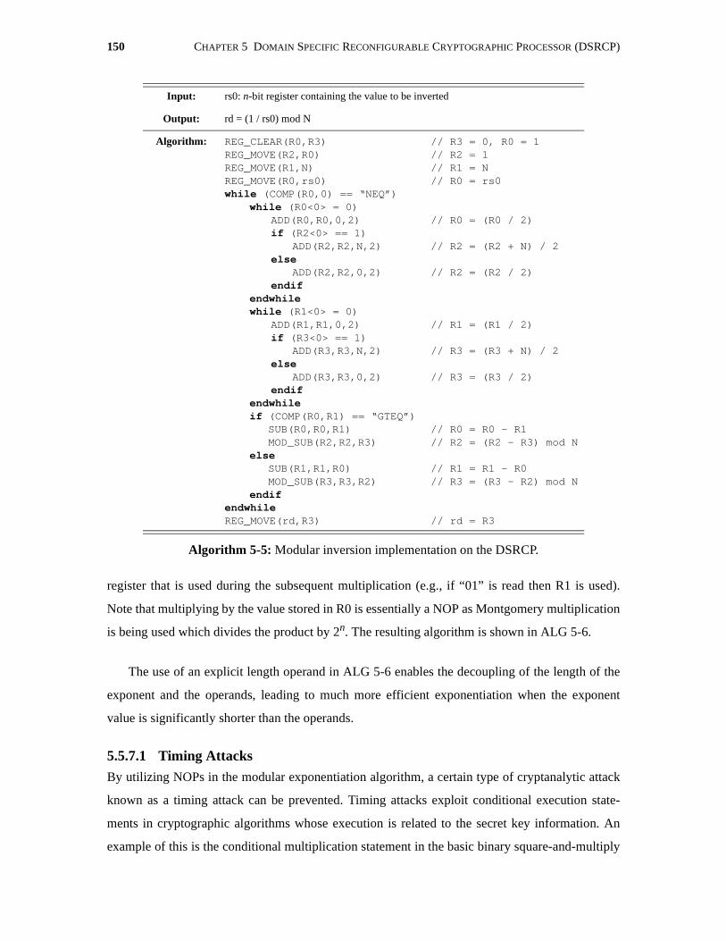
150 CHAPTER 5 DOMAIN SPECIFIC RECONFIGURABLE CRYPTOGRAPHIC PROCESSOR (DSRCP)
register that is used during the subsequent multiplication (e.g., if “01” is read then R1 is used).
Note that multiplying by the value stored in R0 is essentially a NOP as Montgomery multiplication
is being used which divides the product by 2n. The resulting algorithm is shown in ALG 5-6.
The use of an explicit length operand in ALG 5-6 enables the decoupling of the length of the
exponent and the operands, leading to much more efficient exponentiation when the exponent
value is significantly shorter than the operands.
5.5.7.1 Timing Attacks
By utilizing NOPs in the modular exponentiation algorithm, a certain type of cryptanalytic attack
known as a timing attack can be prevented. Timing attacks exploit conditional execution state-
ments in cryptographic algorithms whose execution is related to the secret key information. An
example of this is the conditional multiplication statement in the basic binary square-and-multiply
Input: rs0: n-bit register containing the value to be inverted
Output: rd = (1 / rs0) mod N
Algorithm: REG_CLEAR(R0,R3)REG_MOVE(R2,R0)REG_MOVE(R1,N)REG_MOVE(R0,rs0)while (COMP(R0,0) == “NEQ”)
while (R0<0> = 0)ADD(R0,R0,0,2)if (R2<0> == 1)
ADD(R2,R2,N,2)else
ADD(R2,R2,0,2)endif
endwhilewhile (R1<0> = 0)
ADD(R1,R1,0,2)if (R3<0> == 1)
ADD(R3,R3,N,2)else
ADD(R3,R3,0,2)endif
endwhileif (COMP(R0,R1) == “GTEQ”)
SUB(R0,R0,R1)MOD_SUB(R2,R2,R3)
elseSUB(R1,R1,R0)MOD_SUB(R3,R3,R2)
endifendwhileREG_MOVE(rd,R3)
// R3 = 0, R0 = 1// R2 = 1// R1 = N// R0 = rs0
// R0 = (R0 / 2)
// R2 = (R2 + N) / 2
// R2 = (R2 / 2)
// R1 = (R1 / 2)
// R3 = (R3 + N) / 2
// R3 = (R3 / 2)
// R0 = R0 - R1// R2 = (R2 - R3) mod N
// R1 = R1 - R0// R3 = (R3 - R2) mod N
// rd = R3
Algorithm 5-5: Modular inversion implementation on the DSRCP.
5.5 ALGORITHM IMPLEMENTATION 151
algorithm (ALG 3-14). The resulting variations in execution time, and their correlation to the
secret key information can then be exploited by an attacker in order to recover the secret key infor-
mation. In practice this turns out to be a very powerful weapon in the cryptanalyst’s arsenal.
However, timing attacks are easily thwarted either through the use of blinding techniques
adapted from those used in signature schemes [27], or, as is done in the DSRCP, by eliminating the
variation in execution times. The cost of timing attack immunity is that strings of zeros in the
exponent cannot be exploited to speed up the operation. The loss in efficiency due to this fixed per-
formance, assuming that the probability of any bit in the exponent being set is 1/2 and that Tmult =
Tsquare, is:
(5-5)
Input: rs0: n-bit register containing the value to be exponentiatedrs2: n-bit register containing the Montgomery correction value 22n mod Nlength: 9-bit value representing the length of the exponent stored in Exp
Output: rd = rs0Exp mod N
Algorithm: REG_MOVE(Ps,rs2)
MONT_RED( )
MOD_ADD(R0,Pc,Ps,0)
REG_MOVE(A,rs0)
REG_MOVE(B,rs2)
MONT_MULT( )
MOD_ADD(R1,Pc,Ps,0)
REG_MOVE(A/B,R1)
MONT_MULT( )
MOD_ADD(R2,Pc,Ps,0)
REG_MOVE(B,R2)
MONT_MULT( )
MOD_ADD(R3,Pc,Ps,0)
REG_MOVE(A/B,R0)
for (i=length-1;i>0;i=i-2)MONT_MULT( )
MOD_ADD(A/B,Pc,Ps,0)
MONT_MULT( )
MOD_ADD(A,Pc,Ps,0)
REG_MOVE(B,R<Exp[2i:2i-1]>)
MONT_MULT( )
MOD_ADD(A/B,Pc,Ps,0)
endforMONT_RED_A( )
MOD_ADD(rd,Pc,Ps,0)
// Ps = 22n mod N// (Pc,PS) = 2n mod N// R0 = 2n mod N// A = rs0
// B = 22n mod N// (Pc,Ps) = rs0·2n mod N// R1 = rs0·2n mod N// A,B = rs0·2n mod N// (Pc,Ps) = rs02·2n mod N// R2 = rs02·2n mod N// B = rs02·2n mod N// (Pc,Ps) = rs03·2n mod N// R3 = rs03·2n mod N// A,B = 2n mod N
// (Pc,Ps) = P2·2n mod N// A,B = P2·2n mod N// (Pc,Ps) = P4·2n mod N// A = P4·2n mod N// B = R<j>
// (Pc,Ps) = P4+j·2n mod N// A,B = P4+j·2n mod N
// (Pc,Ps) = PExp mod N// rd = PExp mod N
Algorithm 5-6: Modular exponentiation implementation on the DSRCP.
Tfixed
Tskip------------- 1–
n Tsquaren2---Tmult+⋅
n Tsquaren2--- 1
12---
2–
Tmult
+⋅------------------------------------------------------------------------ 1–
32---nTmult
118
------nTmult
---------------------- 1–1
11------= = =

152 CHAPTER 5 DOMAIN SPECIFIC RECONFIGURABLE CRYPTOGRAPHIC PROCESSOR (DSRCP)
which is approximately 9%. This performance hit is deemed acceptable given the added benefit
that it yields regarding timing attack immunity.
5.5.8 GF(2n) InversionGF(2n) inversion is also implemented directly in hardware so it has no microcoded algorithmic
sequence. Discussion of the resulting implementation is deferred to the design discussion of Sec-
tion 5.6.5.
5.5.9 GF(2n) Addition/Subtraction
GF(2n) addition is equivalent to GF(2n) subtraction, both of which are implemented using compo-
nent-wise XORing of the inputs. The comparator unit is used for this task as it performs this XOR
function implicitly in order to do magnitude comparisons.
5.5.10 GF(2n) MultiplicationGF(2n) multiplication is implemented directly in hardware so it has no microcoded algorithmic
sequence. Discussion of various hardware-based approaches is deferred to the design discussion of
Section 5.6.5.
5.5.11 GF(2n) Exponentiation
GF(2n) exponentiation is implemented in the same manner as modular exponentiation, using a
repeated square-and-multiply approach with an exponent scanning window of size two. {R0, R1,
R2, R3} are now used to store the values {1, rs0, rs02, rs03} which are pre-computed at the start of
the exponentiation operation. Timing attacks are once again addressed by always performing a
multiplication, be it by 1 or some power of rs0. The resulting algorithm is shown in ALG 5-7.
5.5.12 Elliptic Curve Point DoublingThe native elliptic curve point doubling is implemented only over a field of characteristic 2, given
the ISA of the DSRCP though, it is possible to use an off-chip instruction stream to implement
elliptic curve point addition operations in fields of prime characteristic as well via its modular inte-
ger instructions.
Affine co-ordinates are used for elliptic curve point doubling as the storage requirements of a
projective implementation are prohibitively high, as discussed in Section 2.2.1. The fast inversion
times achieved by the DSRCP architecture make an affine co-ordinate based solution faster than
it’s projective equivalent.
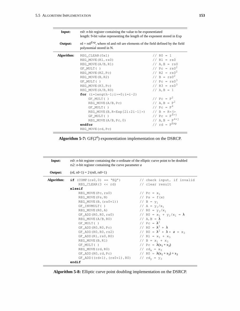
5.5 ALGORITHM IMPLEMENTATION 153
Input: rs0: n-bit register containing the value to be exponentiatedlength: 9-bit value representing the length of the exponent stored in Exp
Output: rd = rs0Exp, where rd and rs0 are elements of the field defined by the field polynomial stored in N.
Algorithm: REG_CLEAR(0x1)
REG_MOVE(R1,rs0)
REG_MOVE(A/B,R1)
GF_MULT( )
REG_MOVE(R2,Pc)
REG_MOVE(B,R2)
GF_MULT( )
REG_MOVE(R3,Pc)
REG_MOVE(A/B,R0)
for (i=length-1;i>=0;i=i-2)GF_MULT( )
REG_MOVE(A/B,Pc)
GF_MULT( )
REG_MOVE(B,R<Exp[2i:2i-1]>)
GF_MULT( )
REG_MOVE(A/B,Pc,0)
endforREG_MOVE(rd,Pc)
// R0 = 1
// R1 = rs0
// A,B = rs0
// Pc = rs02
// R2 = rs02
// B = rs02
// Pc = rs03
// R3 = rs03
// A,B = 1
// Pc = P2
// A,B = P2
// Pc = P4
// B = R<j>// Pc = P4+j
// A,B = P4+j
// rd = PExp
Algorithm 5-7: GF(2n) exponentiation implementation on the DSRCP.
Input: rs0: n-bit register containing the x-ordinate of the elliptic curve point to be doubledrs2: n-bit register containing the curve parameter a
Output: (rd, rd+1) = 2·(rs0, rs0+1)
Algorithm: if (COMP(rs0,0) == “EQ”)REG_CLEAR(3 << rd)
elseifREG_MOVE(Pc,rs0) REG_MOVE(Ps,N)REG_MOVE(B,(rs0+1)) GF_INVMULT( ) REG_MOVE(R0,A) GF_ADD(R0,R0,rs0) REG_MOVE(A/B,R0) GF_MULT( )
GF_ADD(R0,R0,Pc)
GF_ADD(R0,R0,rs2)
GF_ADD(R1,rs0,R0)
REG_MOVE(B,R1)
GF_MULT( )
REG_MOVE(rd,R0)
GF_ADD(R0,rd,Pc)
GF_ADD((rd+1),(rs0+1),R0)
endif
// check input, if invalid// clear result
// Pc = x1// Ps = f(x)// B = y1// A = y1/x1// R0 = y1/x1// R0 = x1 + y1/x1 = λ// A,B = λ// Pc = λ2// R0 = λ2 + λ// R0 = λ2 + λ + a = x3// R1 = x1 + x3// B = x1 + x3// Pc = λ(x1 + x3)// rdx = x3// R0 = λ(x1 + x3) + x3// rdy = y3
Algorithm 5-8: Elliptic curve point doubling implementation on the DSRCP.
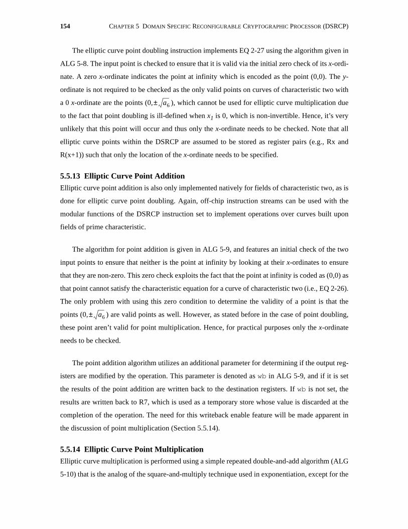
154 CHAPTER 5 DOMAIN SPECIFIC RECONFIGURABLE CRYPTOGRAPHIC PROCESSOR (DSRCP)
The elliptic curve point doubling instruction implements EQ 2-27 using the algorithm given in
ALG 5-8. The input point is checked to ensure that it is valid via the initial zero check of its x-ordi-
nate. A zero x-ordinate indicates the point at infinity which is encoded as the point (0,0). The y-
ordinate is not required to be checked as the only valid points on curves of characteristic two with
a 0 x-ordinate are the points (0, ), which cannot be used for elliptic curve multiplication due
to the fact that point doubling is ill-defined when x1 is 0, which is non-invertible. Hence, it’s very
unlikely that this point will occur and thus only the x-ordinate needs to be checked. Note that all
elliptic curve points within the DSRCP are assumed to be stored as register pairs (e.g., Rx and
R(x+1)) such that only the location of the x-ordinate needs to be specified.
5.5.13 Elliptic Curve Point Addition
Elliptic curve point addition is also only implemented natively for fields of characteristic two, as is
done for elliptic curve point doubling. Again, off-chip instruction streams can be used with the
modular functions of the DSRCP instruction set to implement operations over curves built upon
fields of prime characteristic.
The algorithm for point addition is given in ALG 5-9, and features an initial check of the two
input points to ensure that neither is the point at infinity by looking at their x-ordinates to ensure
that they are non-zero. This zero check exploits the fact that the point at infinity is coded as (0,0) as
that point cannot satisfy the characteristic equation for a curve of characteristic two (i.e., EQ 2-26).
The only problem with using this zero condition to determine the validity of a point is that the
points (0, ) are valid points as well. However, as stated before in the case of point doubling,
these point aren’t valid for point multiplication. Hence, for practical purposes only the x-ordinate
needs to be checked.
The point addition algorithm utilizes an additional parameter for determining if the output reg-
isters are modified by the operation. This parameter is denoted as wb in ALG 5-9, and if it is set
the results of the point addition are written back to the destination registers. If wb is not set, the
results are written back to R7, which is used as a temporary store whose value is discarded at the
completion of the operation. The need for this writeback enable feature will be made apparent in
the discussion of point multiplication (Section 5.5.14).
5.5.14 Elliptic Curve Point MultiplicationElliptic curve multiplication is performed using a simple repeated double-and-add algorithm (ALG
5-10) that is the analog of the square-and-multiply technique used in exponentiation, except for the
a6±
a6±
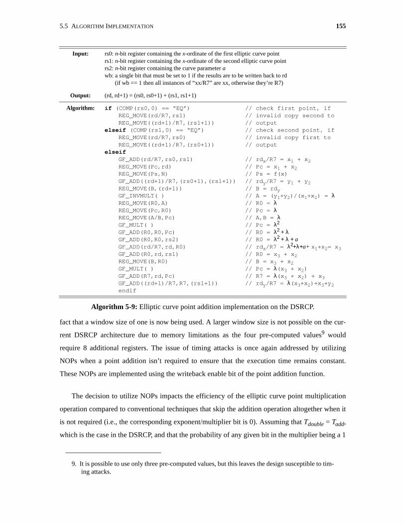
5.5 ALGORITHM IMPLEMENTATION 155
fact that a window size of one is now being used. A larger window size is not possible on the cur-
rent DSRCP architecture due to memory limitations as the four pre-computed values9 would
require 8 additional registers. The issue of timing attacks is once again addressed by utilizing
NOPs when a point addition isn’t required to ensure that the execution time remains constant.
These NOPs are implemented using the writeback enable bit of the point addition function.
The decision to utilize NOPs impacts the efficiency of the elliptic curve point multiplication
operation compared to conventional techniques that skip the addition operation altogether when it
is not required (i.e., the corresponding exponent/multiplier bit is 0). Assuming that Tdouble = Tadd,
which is the case in the DSRCP, and that the probability of any given bit in the multiplier being a 1
Input: rs0: n-bit register containing the x-ordinate of the first elliptic curve pointrs1: n-bit register containing the x-ordinate of the second elliptic curve pointrs2: n-bit register containing the curve parameter awb: a single bit that must be set to 1 if the results are to be written back to rd
(if wb == 1 then all instances of “xx/R7” are xx, otherwise they’re R7)
Output: (rd, rd+1) = (rs0, rs0+1) + (rs1, rs1+1)
Algorithm: if (COMP(rs0,0) == “EQ”)REG_MOVE(rd/R7,rs1)REG_MOVE((rd+1)/R7,(rs1+1))
elseif (COMP(rs1,0) == “EQ”)REG_MOVE(rd/R7,rs0)REG_MOVE((rd+1)/R7,(rs0+1))
elseifGF_ADD(rd/R7,rs0,rs1) REG_MOVE(Pc,rd) REG_MOVE(Ps,N)GF_ADD((rd+1)/R7,(rs0+1),(rs1+1)) REG_MOVE(B,(rd+1)) GF_INVMULT( ) REG_MOVE(R0,A) REG_MOVE(Pc,R0) REG_MOVE(A/B,Pc)GF_MULT( )
GF_ADD(R0,R0,Pc)
GF_ADD(R0,R0,rs2)
GF_ADD(rd/R7,rd,R0)
GF_ADD(R0,rd,rs1)
REG_MOVE(B,R0)
GF_MULT( )
GF_ADD(R7,rd,Pc)
GF_ADD((rd+1)/R7,R7,(rs1+1))
endif
// check first point, if// invalid copy second to// output// check second point, if// invalid copy first to // output
// rdx/R7 = x1 + x2// Pc = x1 + x2// Ps = f(x)// rdy/R7 = y1 + y2// B = rdy// A = (y1+y2)/(x1+x2) = λ// R0 = λ // Pc = λ // A,B = λ// Pc = λ2
// R0 = λ2 + λ// R0 = λ2 + λ + a// rdx/R7 = λ2+λ+a+ x1+x2= x3// R0 = x3 + x2// B = x3 + x2// Pc = λ(x3 + x2)// R7 = λ(x3 + x2) + x3// rdy/R7 = λ(x3+x2)+x3+y2
Algorithm 5-9: Elliptic curve point addition implementation on the DSRCP.
9. It is possible to use only three pre-computed values, but this leaves the design susceptible to tim-ing attacks.
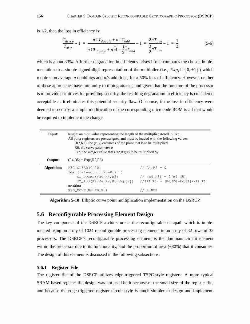
156 CHAPTER 5 DOMAIN SPECIFIC RECONFIGURABLE CRYPTOGRAPHIC PROCESSOR (DSRCP)
is 1/2, then the loss in efficiency is:
(5-6)
which is about 33%. A further degradation in efficiency arises if one compares the chosen imple-
mentation to a simple signed-digit representation of the multiplier (i.e., ) which
requires on average n doublings and n/3 additions, for a 50% loss of efficiency. However, neither
of these approaches have immunity to timing attacks, and given that the function of the processor
is to provide primitives for providing security, the resulting degradation in efficiency is considered
acceptable as it eliminates this potential security flaw. Of course, if the loss in efficiency were
deemed too costly, a simple modification of the corresponding microcode ROM is all that would
be required to implement the change.
5.6 Reconfigurable Processing Element DesignThe key component of the DSRCP architecture is the reconfigurable datapath which is imple-
mented using an array of 1024 reconfigurable processing elements in an array of 32 rows of 32
processors. The DSRCP’s reconfigurable processing element is the dominant circuit element
within the processor due to its functionality, and the proportion of area (~80%) that it consumes.
The design of this element is discussed in the following subsections.
5.6.1 Register File
The register file of the DSRCP utilizes edge-triggered TSPC-style registers. A more typical
SRAM-based register file design was not used both because of the small size of the register file,
and because the edge-triggered register circuit style is much simpler to design and implement,
Input: length: an n-bit value representing the length of the multiplier stored in Exp.All other registers are pre-assigned and must be loaded with the following values:
(R2,R3): the (x, y) ordinates of the point that is to be multipliedR6: the curve parameter aExp: the integer value that (R2,R3) is to be multiplied by
Output: (R4,R5) = Exp·(R2,R3)
Algorithm: REG_CLEAR(0x30)for (i=length-1;i>=0;i--)
EC_DOUBLE(R4,R4,R6)EC_ADD(R4,R4,R2,R6,Exp[i])
endforREG_MOVE(R0,R0,R0)
// R4,R5 = 0
// (R4,R5) = 2(R4,R5)//(R4,R5) = (R4,R5)+Exp[i]·(R2,R3)
// a NOP
Algorithm 5-10: Elliptic curve point multiplication implementation on the DSRCP.
Tdsrcp
Tskip-------------- 1–
n Tdouble n Tadd⋅+⋅
n Tdouble n 112---–
Tadd+⋅--------------------------------------------------------------- 1–
2nTadd
32---nTadd
----------------- 1–13---= = =
Expi 0 1±,{ }∈
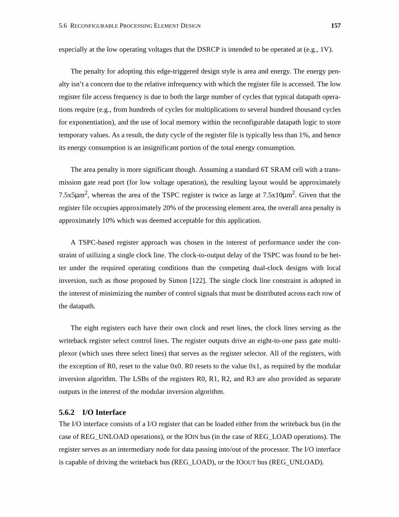
5.6 RECONFIGURABLE PROCESSING ELEMENT DESIGN 157
especially at the low operating voltages that the DSRCP is intended to be operated at (e.g., 1V).
The penalty for adopting this edge-triggered design style is area and energy. The energy pen-
alty isn’t a concern due to the relative infrequency with which the register file is accessed. The low
register file access frequency is due to both the large number of cycles that typical datapath opera-
tions require (e.g., from hundreds of cycles for multiplications to several hundred thousand cycles
for exponentiation), and the use of local memory within the reconfigurable datapath logic to store
temporary values. As a result, the duty cycle of the register file is typically less than 1%, and hence
its energy consumption is an insignificant portion of the total energy consumption.
The area penalty is more significant though. Assuming a standard 6T SRAM cell with a trans-
mission gate read port (for low voltage operation), the resulting layout would be approximately
7.5x5µm2, whereas the area of the TSPC register is twice as large at 7.5x10µm2. Given that the
register file occupies approximately 20% of the processing element area, the overall area penalty is
approximately 10% which was deemed acceptable for this application.
A TSPC-based register approach was chosen in the interest of performance under the con-
straint of utilizing a single clock line. The clock-to-output delay of the TSPC was found to be bet-
ter under the required operating conditions than the competing dual-clock designs with local
inversion, such as those proposed by Simon [122]. The single clock line constraint is adopted in
the interest of minimizing the number of control signals that must be distributed across each row of
the datapath.
The eight registers each have their own clock and reset lines, the clock lines serving as the
writeback register select control lines. The register outputs drive an eight-to-one pass gate multi-
plexor (which uses three select lines) that serves as the register selector. All of the registers, with
the exception of R0, reset to the value 0x0. R0 resets to the value 0x1, as required by the modular
inversion algorithm. The LSBs of the registers R0, R1, R2, and R3 are also provided as separate
outputs in the interest of the modular inversion algorithm.
5.6.2 I/O InterfaceThe I/O interface consists of a I/O register that can be loaded either from the writeback bus (in the
case of REG_UNLOAD operations), or the IOIN bus (in the case of REG_LOAD operations). The
register serves as an intermediary node for data passing into/out of the processor. The I/O interface
is capable of driving the writeback bus (REG_LOAD), or the IOOUT bus (REG_UNLOAD).
158 CHAPTER 5 DOMAIN SPECIFIC RECONFIGURABLE CRYPTOGRAPHIC PROCESSOR (DSRCP)
5.6.3 Magnitude ComparatorThe DSRCP design requires a magnitude comparator that is capable of resolving the relative mag-
nitudes of two operands up to 1024 bits long within a single 20ns cycle at the desired operating
voltage of 1V. This is accomplished using a fast, tree-based technique that is shown in Figure 5-6,
and which is similar to the sign detection technique used within the ESEP. The comparator first
encodes the inputs based on a bit-by-bit comparison of the two operands to form the signals
, and . Once in this format, two adjacent, encoded bit posi-
tions can be compared using the relations , and
, the outputs of which are passed to the next level of the
comparator tree. At each stage, the number of comparisons are reduced by a factor of two, hence
the tree has depth log2 n, where n is the number of bits in the operands.
The comparator is partitioned into thirty-two 32-bit sections, or one section per row. The final
stage of each of these 32 comparisons utilizes an enable signal that either performs the aforemen-
tioned comparison if the row is enabled, or outputs an equal signal in the event that the row has
been disabled in order to prevent any data remaining in the upper, unused portions of the register
from corrupting the comparison. The resulting comparator circuit is shown in Figure 5-6.
5.6.4 Carry Bypass Add/Subtract UnitThe DSRCP requires non-redundant addition/subtraction operations that must operate on operands
that can be up to 1024 bits long. To complicate matters further, this operation must be performed
EQi op1i op2i⊕= GTi op1i op2i⋅=
EQj 1 i,+ EQj 2 i, EQj 2 i 1+,⋅=
GTj 1 i,+ GTj 2i 1+, GTj 2i, EQj 2i 1+,⋅+=
Figure 5-6: Tree-based magnitude comparator topology used in the DSRCP.
. . .. . .
. . .
. . .
. . .
Operand encoder
. . . . . .log2n levels
GT, EQ flags
(EQ’i,GT’i)
(EQi-1,GTi-1)
(EQi,GTi)
EQi
GTi
EQi
EQi-1
GTi-1
Operand 1 Operand 2
(EQi,GTi)
op2iop1i
EQiGTi
rowen31 rowen0

5.6 RECONFIGURABLE PROCESSING ELEMENT DESIGN 159
as quickly as possible, in as small an area as possible, and preferably using a modular bitsliced
implementation.
There are a wealth of fast addition techniques available to choose from such as carry-looka-
head, carry-bypass/skip, and carry-select. Carry-lookahead is the most time efficient as a hierarchi-
cal approach can compute n-bit additions in O(log2 n) delay, but its area overhead precludes its use
within the DSRCP. On the other hand, conventional hierarchical carry-select and carry-bypass/skip
implementations have O( ) delay, but don’t lend themselves well to a modular, bit-sliced imple-
mentation as they require very wide AND structures and multiplexors that won’t fit within the area
constraints of the DSRCP’s processing element.
However, the modified carry-bypass/skip adder proposed in [113] yields a delay of O( ),
while lending itself to a very efficient, bitsliced implementation. The main difference between the
proposed adder and a conventional carry-bypass adder is that the propagate signal pi is generated
in a serialized fashion and then used to determine if the group carry-in cj will affect the individual
bitslice. If so, then cj is XORed with the sum output di to produce the correct sum value si, as
shown in Figure 5-7. This approach is much better-suited to the bitsliced requirements of the
DSRCP as the wide AND structures of the conventional carry-bypass/skip adder are now trans-
formed to a serialized AND function that can be distributed between the bitslices very efficiently,
as shown in Figure 5-7.
Using this basic bitslice, the full addition is separated into groups of increasing length, each of
which computes its sum assuming a carry-in of zero. When the carry-out of the previous stage is
determined, both the output sum bits of the current stage and the group carry-out are corrected
n
n
Figure 5-7: Modified bitsliced carry-bypass adder [113].
xiyi
gi
c
s
gi+1
p
pipi+1
cin
si
p1
g1
p2
g2
0
1. . .
pi+1
gi+1
gi+2
pi+2
x0 y0
cin
pi
gi
0
1
x1 y1 xi yi xi+1 yi+1
s0 s1 si si+1
. . .
cj
Full-adder with propagateoutput corresponding to
p xi yi⊕( )=
di
group carrygenerator
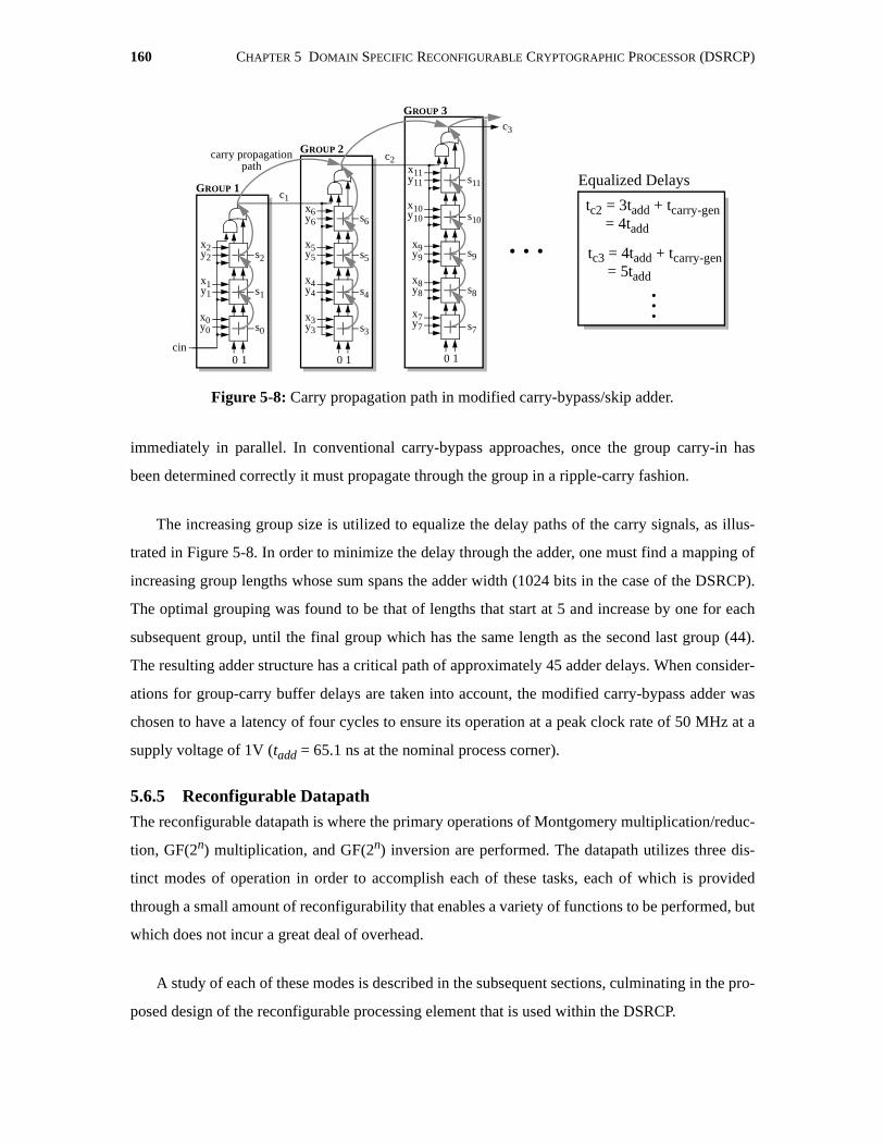
160 CHAPTER 5 DOMAIN SPECIFIC RECONFIGURABLE CRYPTOGRAPHIC PROCESSOR (DSRCP)
immediately in parallel. In conventional carry-bypass approaches, once the group carry-in has
been determined correctly it must propagate through the group in a ripple-carry fashion.
The increasing group size is utilized to equalize the delay paths of the carry signals, as illus-
trated in Figure 5-8. In order to minimize the delay through the adder, one must find a mapping of
increasing group lengths whose sum spans the adder width (1024 bits in the case of the DSRCP).
The optimal grouping was found to be that of lengths that start at 5 and increase by one for each
subsequent group, until the final group which has the same length as the second last group (44).
The resulting adder structure has a critical path of approximately 45 adder delays. When consider-
ations for group-carry buffer delays are taken into account, the modified carry-bypass adder was
chosen to have a latency of four cycles to ensure its operation at a peak clock rate of 50 MHz at a
supply voltage of 1V (tadd = 65.1 ns at the nominal process corner).
5.6.5 Reconfigurable DatapathThe reconfigurable datapath is where the primary operations of Montgomery multiplication/reduc-
tion, GF(2n) multiplication, and GF(2n) inversion are performed. The datapath utilizes three dis-
tinct modes of operation in order to accomplish each of these tasks, each of which is provided
through a small amount of reconfigurability that enables a variety of functions to be performed, but
which does not incur a great deal of overhead.
A study of each of these modes is described in the subsequent sections, culminating in the pro-
posed design of the reconfigurable processing element that is used within the DSRCP.
Figure 5-8: Carry propagation path in modified carry-bypass/skip adder.
0 1 0 1 0 1
x0y0
cin
s0
s1
s2
s6
s5
s4
s3
s10
s11
s9
s8
s7
c1
c2
c3
x1y1
x2y2
x3y3
x4y4
x5y5
x6y6
x7y7
x8y8
x9y9
x10y10
x11y11
. . .
carry propagationpath
GROUP 1
GROUP 2
GROUP 3
tc2 = 3tadd + tcarry-gen= 4tadd
. . .
tc3 = 4tadd + tcarry-gen= 5tadd
Equalized Delays
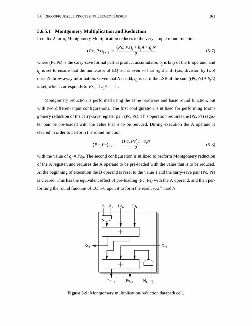
5.6 RECONFIGURABLE PROCESSING ELEMENT DESIGN 161
5.6.5.1 Montgomery Multiplication and ReductionIn radix-2 form, Montgomery Multiplication reduces to the very simple round function
(5-7)
where (Pc,Ps) is the carry-save format partial product accumulator, bj is bit j of the B operand, and
qj is set to ensure that the numerator of EQ 5-5 is even so that right shift (i.e., division by two)
doesn’t throw away information. Given that N is odd, qj is set if the LSB of the sum ((Pc,Ps) + bjA)
is set, which corresponds to .
Montgomery reduction is performed using the same hardware and basic round function, but
with two different input configurations. The first configuration is utilized for performing Mont-
gomery reduction of the carry-save register pair (Pc, Ps). This operation requires the (Pc, Ps) regis-
ter pair be pre-loaded with the value that is to be reduced. During execution the A operand is
cleared in order to perform the round function
(5-8)
with the value of qj = Ps0. The second configuration is utilized to perform Montgomery reduction
of the A register, and requires the A operand to be pre-loaded with the value that is to be reduced.
At the beginning of execution the B operand is reset to the value 1 and the carry-save pair (Pc, Ps)
is cleared. This has the equivalent effect of pre-loading (Pc, Ps) with the A operand, and then per-
forming the round function of EQ 5-8 upon it to form the result A·2-n mod N.
Pc Ps,( )j 1+
Pc Ps,( )j bjA qjN+ +
2----------------------------------------------------=
Ps0 bjA⊕ 1=
Pc Ps,( )j 1+
Pc Ps,( )j qjN+
2-------------------------------------=
Figure 5-9: Montgomery multiplication/reduction datapath cell.
Xci Xci-1
Ni
Ai Pci-1 Psibj
qjPsi-1Pci-1
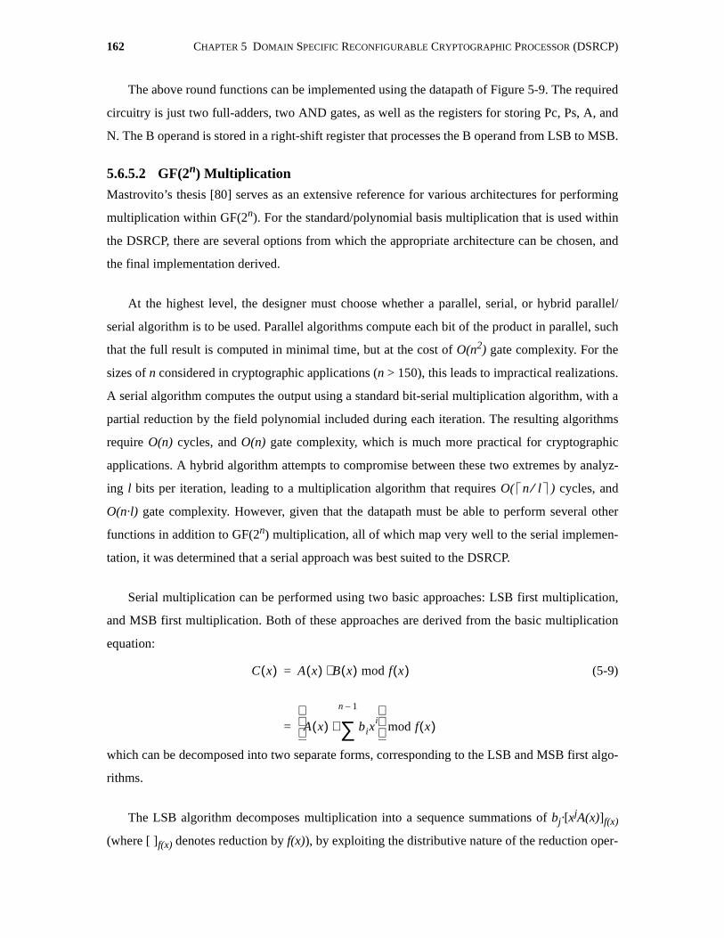
162 CHAPTER 5 DOMAIN SPECIFIC RECONFIGURABLE CRYPTOGRAPHIC PROCESSOR (DSRCP)
The above round functions can be implemented using the datapath of Figure 5-9. The required
circuitry is just two full-adders, two AND gates, as well as the registers for storing Pc, Ps, A, and
N. The B operand is stored in a right-shift register that processes the B operand from LSB to MSB.
5.6.5.2 GF(2n) Multiplication
Mastrovito’s thesis [80] serves as an extensive reference for various architectures for performing
multiplication within GF(2n). For the standard/polynomial basis multiplication that is used within
the DSRCP, there are several options from which the appropriate architecture can be chosen, and
the final implementation derived.
At the highest level, the designer must choose whether a parallel, serial, or hybrid parallel/
serial algorithm is to be used. Parallel algorithms compute each bit of the product in parallel, such
that the full result is computed in minimal time, but at the cost of O(n2) gate complexity. For the
sizes of n considered in cryptographic applications (n > 150), this leads to impractical realizations.
A serial algorithm computes the output using a standard bit-serial multiplication algorithm, with a
partial reduction by the field polynomial included during each iteration. The resulting algorithms
require O(n) cycles, and O(n) gate complexity, which is much more practical for cryptographic
applications. A hybrid algorithm attempts to compromise between these two extremes by analyz-
ing l bits per iteration, leading to a multiplication algorithm that requires O( ) cycles, and
O(n·l) gate complexity. However, given that the datapath must be able to perform several other
functions in addition to GF(2n) multiplication, all of which map very well to the serial implemen-
tation, it was determined that a serial approach was best suited to the DSRCP.
Serial multiplication can be performed using two basic approaches: LSB first multiplication,
and MSB first multiplication. Both of these approaches are derived from the basic multiplication
equation:
(5-9)
which can be decomposed into two separate forms, corresponding to the LSB and MSB first algo-
rithms.
The LSB algorithm decomposes multiplication into a sequence summations of bj·[xjA(x)]f(x)
(where [ ]f(x) denotes reduction by f(x)), by exploiting the distributive nature of the reduction oper-
n l⁄
C x( ) A x( ) B x( ) mod f x( )⋅
A x( ) bixi
n 1–
∑⋅
mod f x( )
=
=
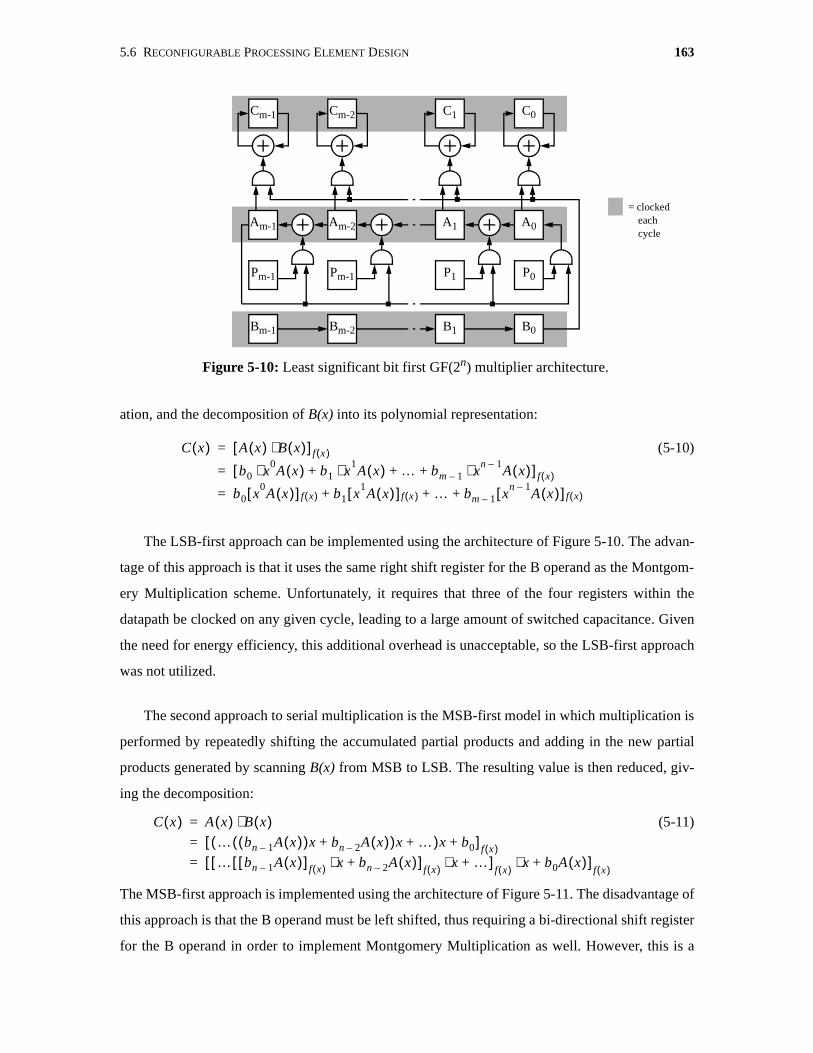
5.6 RECONFIGURABLE PROCESSING ELEMENT DESIGN 163
ation, and the decomposition of B(x) into its polynomial representation:
(5-10)
The LSB-first approach can be implemented using the architecture of Figure 5-10. The advan-
tage of this approach is that it uses the same right shift register for the B operand as the Montgom-
ery Multiplication scheme. Unfortunately, it requires that three of the four registers within the
datapath be clocked on any given cycle, leading to a large amount of switched capacitance. Given
the need for energy efficiency, this additional overhead is unacceptable, so the LSB-first approach
was not utilized.
The second approach to serial multiplication is the MSB-first model in which multiplication is
performed by repeatedly shifting the accumulated partial products and adding in the new partial
products generated by scanning B(x) from MSB to LSB. The resulting value is then reduced, giv-
ing the decomposition:
(5-11)
The MSB-first approach is implemented using the architecture of Figure 5-11. The disadvantage of
this approach is that the B operand must be left shifted, thus requiring a bi-directional shift register
for the B operand in order to implement Montgomery Multiplication as well. However, this is a
C x( ) A x( ) B x( )⋅[ ] f x( )
b0 x0A x( ) b1 x
1A x( ) … bm 1– x
n 1–A x( )⋅+ +⋅+⋅[ ] f x( )
b0 x0A x( )[ ] f x( ) b1 x
1A x( )[ ] f x( ) … bm 1– x
n 1–A x( )[ ] f x( )+ + +
=
=
=
Figure 5-10: Least significant bit first GF(2n) multiplier architecture.
Bm-1
Cm-1
Bm-2 B1 B0
Am-1
Pm-1
Am-2
Cm-2
Pm-1
C1
A1
P1
A0
C0
P0
= clockedeachcycle
C x( ) A x( ) B x( )⋅… bn 1– A x( )( )x bn 2– A x( )+( )x …+( )x b0+[ ] f x( )… bn 1– A x( )[ ] f x( ) x bn 2– A x( )+⋅[ ]
f x( ) x …+⋅[ ]f x( ) x b0A x( )+⋅[ ]
f x( )
=
=
=
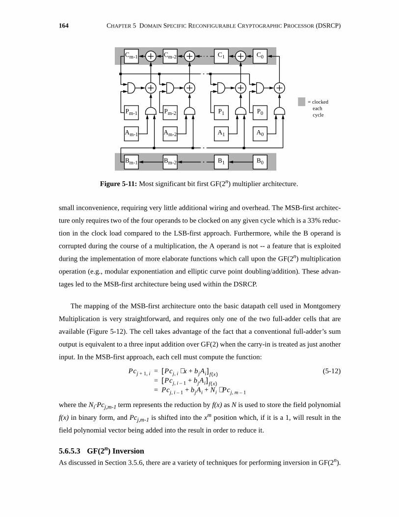
164 CHAPTER 5 DOMAIN SPECIFIC RECONFIGURABLE CRYPTOGRAPHIC PROCESSOR (DSRCP)
small inconvenience, requiring very little additional wiring and overhead. The MSB-first architec-
ture only requires two of the four operands to be clocked on any given cycle which is a 33% reduc-
tion in the clock load compared to the LSB-first approach. Furthermore, while the B operand is
corrupted during the course of a multiplication, the A operand is not -- a feature that is exploited
during the implementation of more elaborate functions which call upon the GF(2n) multiplication
operation (e.g., modular exponentiation and elliptic curve point doubling/addition). These advan-
tages led to the MSB-first architecture being used within the DSRCP.
The mapping of the MSB-first architecture onto the basic datapath cell used in Montgomery
Multiplication is very straightforward, and requires only one of the two full-adder cells that are
available (Figure 5-12). The cell takes advantage of the fact that a conventional full-adder’s sum
output is equivalent to a three input addition over GF(2) when the carry-in is treated as just another
input. In the MSB-first approach, each cell must compute the function:
(5-12)
where the Ni·Pcj,m-1 term represents the reduction by f(x) as N is used to store the field polynomial
f(x) in binary form, and Pcj,m-1 is shifted into the xm position which, if it is a 1, will result in the
field polynomial vector being added into the result in order to reduce it.
5.6.5.3 GF(2n) Inversion
As discussed in Section 3.5.6, there are a variety of techniques for performing inversion in GF(2n).
Figure 5-11: Most significant bit first GF(2n) multiplier architecture.
Am-1
Bm-1
Pm-1
Cm-1
Am-2
Bm-2
Pm-2
Cm-2
A1
B1
P1
C1
A0
B0
P0
C0
= clockedeachcycle
Pcj 1 i,+ Pcj i, x bjAi+⋅[ ] f x( )Pcj i 1–, bjAi+[ ] f x( )
Pcj i 1–, bjAi Ni Pcj m 1–,⋅+ +
===
5.6 RECONFIGURABLE PROCESSING ELEMENT DESIGN 165
In hardware, a very simple, and as it turns out very efficient, means of implementing inversion uti-
lizes the binary extended euclidean algorithm shown in ALG 5-11. The algorithm is modified to
perform a multiplication in concurrency with the inversion, by initializing the Y variable to be the
multiplier value (if no multiplication is required, the Y register can simply be initialized with the
value 1). This optimization provides significant savings during elliptic curve point operations as it
eliminates one multiplication, reducing the total cycle count by approximately 18%. The algorithm
can be further optimized by parallelizing the two embedded while loops, which effectively halves
the number of cycles required as the dominant amount of time is spent in this portion of the algo-
rithm. The net result of these optimizations is a universal inversion implementation that works over
any field of order and takes at most four multiplication times (Tmult = n cycles), and
on average 3.3Tmult in order to invert (and multiply) an element of GF(2n).
Implementing ALG 5-11 on the datapath cell used in both Montgomery and GF(2n) multipli-
cation requires some degree of reconfigurability so that the computational resources can be re-used
to perform different parts of ALG 5-11. The basic requirements are two two-input adders over
GF(2) to perform each of the parallel while loops, and the two summations in each branch of the IF
clause. Since all operations are performed in parallel, each iteration of the parallel while loops
requires one cycle to perform the actual operations. An additional cycle is incurred when the exit
condition of the parallel while loops is satisfied (i.e., W0 = X0 = 1) as it must be detected via an
additional iteration of the loop. The second part of the algorithm requires a single cycle as well.
The two datapath adders can be used as two input GF(2) adders by zeroing one of their inputs and
Figure 5-12: GF(2n) multiplication datapath cell.
Ai Pci-1bj
Pci
Niqj
8 n 1024≤ ≤
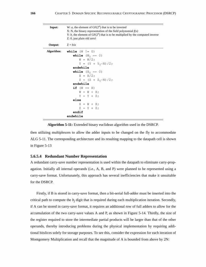
166 CHAPTER 5 DOMAIN SPECIFIC RECONFIGURABLE CRYPTOGRAPHIC PROCESSOR (DSRCP)
then utilizing multiplexors to allow the adder inputs to be changed on the fly to accommodate
ALG 5-11. The corresponding architecture and its resulting mapping to the datapath cell is shown
in Figure 5-13
5.6.5.4 Redundant Number RepresentationA redundant carry-save number representation is used within the datapath to eliminate carry-prop-
agation. Initially all internal operands (i.e., A, B, and P) were planned to be represented using a
carry-save format. Unfortunately, this approach has several inefficiencies that make it unsuitable
for the DSRCP.
Firstly, if B is stored in carry-save format, then a bit-serial full-adder must be inserted into the
critical path to compute the bj digit that is required during each multiplication iteration. Secondly,
if A can be stored in carry-save format, it requires an additional row of full adders to allow for the
accumulation of the two carry-save values A and P, as shown in Figure 5-14. Thirdly, the size of
the register required to store the intermediate partial products will be larger than that of the other
operands, thereby introducing problems during the physical implementation by requiring addi-
tional bitslices solely for storage purposes. To see this, consider the expression for each iteration of
Montgomery Multiplication and recall that the magnitude of A is bounded from above by 2N:
Input: W: a, the element of GF(2n) that is to be invertedX: N, the binary representation of the field polynomial f(x)Y: b, the element of GF(2n) that is to be multiplied by the computed inverseZ: 0, just plain old zero!
Output: Z = b/a
Algorithm: while (W != 0)while (W0 == 0)
W = W/2;Y = (Y + Y0·N)/2;
endwhilewhile (X0 == 0)
X = X/2;Z = (Z + Z0·N)/2;
endwhileif (W >= X)
W = W + X;Y = Y + Z;
elseX = W + X;Z = Y + Z;
endifendwhile
Algorithm 5-11: Extended binary euclidean algorithm used in the DSRCP.

5.6 RECONFIGURABLE PROCESSING ELEMENT DESIGN 167
. . .
(5-13)
Thus, (n + 1) bits will be required for both Pc and Ps. From an algorithmic standpoint, the
increased magnitude of the partial product would require additional iterations of Montgomery’s
Multiplication Algorithm, increasing the control complexity as multiplication would now be a spe-
cial case, and require its own unique correction value (i.e., 22(n+1) as opposed to the value 22n used
in both Montgomery reduction and modular reduction.
However, if only the partial product is stored in redundant format then repeated modular mul-
tiplications/squarings will require a modular addition operation between operations. This intro-
duces a 10 cycle overhead per multiplication operation, which is approximately 1-2% overhead on
a 512 or 1024 bit modular exponentiation. Since all of the aforementioned problems can be
Pc Ps,( )0 0Pc Ps,( )1 Pc Ps,( )0 bj Ac As,( ) qjN+ +( ) 2N N+( ) 2⁄< 3N 2⁄Pc Ps,( )2 Pc Ps,( )2 bj Ac As,( ) qjN+ +( ) 3N 2⁄ 2N N+ +( ) 2⁄< 9N 4⁄
== == =
Ni
Ai Pci BiPsi
To Ai/Bi/Bi-1 1
1
To
NY ZW NZ X
W X
Y Z
W/2
S0
a
X/2
S1
N
Y/2S1/2
S1b
Z/2S0/2
S10
Figure 5-13: Basic GF(2n) inversion architecture resulting datapath cell.
0 1 0 1 0 1sel1 sel1sel0
Y + ZY + N
W + XZ + N
sel1:0
0 11 0
S0 S1
S0 S1
Psi/Pci/Ai-1
0
0W: PcX: PsY: BZ: A
Pc Ps,( )k 3N 2i–
i 1=
k
∑ 3N 11
2i
----– 3N<= =
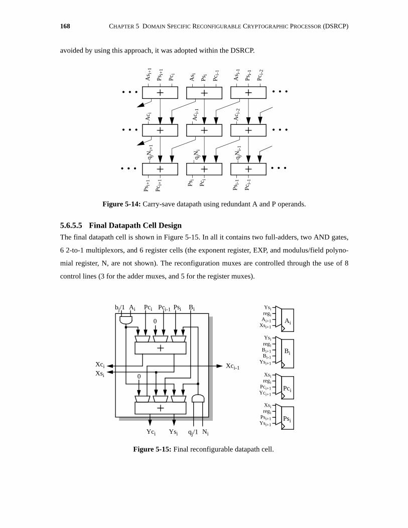
168 CHAPTER 5 DOMAIN SPECIFIC RECONFIGURABLE CRYPTOGRAPHIC PROCESSOR (DSRCP)
avoided by using this approach, it was adopted within the DSRCP.
5.6.5.5 Final Datapath Cell DesignThe final datapath cell is shown in Figure 5-15. In all it contains two full-adders, two AND gates,
6 2-to-1 multiplexors, and 6 register cells (the exponent register, EXP, and modulus/field polyno-
mial register, N, are not shown). The reconfiguration muxes are controlled through the use of 8
control lines (3 for the adder muxes, and 5 for the register muxes).
As i
Ps i
Pc i
-1
Figure 5-14: Carry-save datapath using redundant A and P operands.
As i
-1
Ps i
-1
Pc i
-2
As i
+1
Ps i
+1
Pc i
Ac i
-2
Ac i
-1
Ac i
. . .. . .
. . .. . .
q jN
i-1
q jN
i
q jN
i+1
Ps i
-1
Pc i
-1Ps i
Pc i
Psi+
1
Pci+
1
. . .. . .
Figure 5-15: Final reconfigurable datapath cell.
Ai Psibj/1 Pci Pci-1 Bi
Niqj/1
0
Xci-1XciXsi
Yci Ysi
Ysiregi
Ai+1Xsi+1
regiBi+1Bi-1
Ysi+1
Xsiregi
Pci+1Yci+1
Xsiregi
Psi+1Ysi+1
Ai
Bi
Pci
Psi
Ysi
0
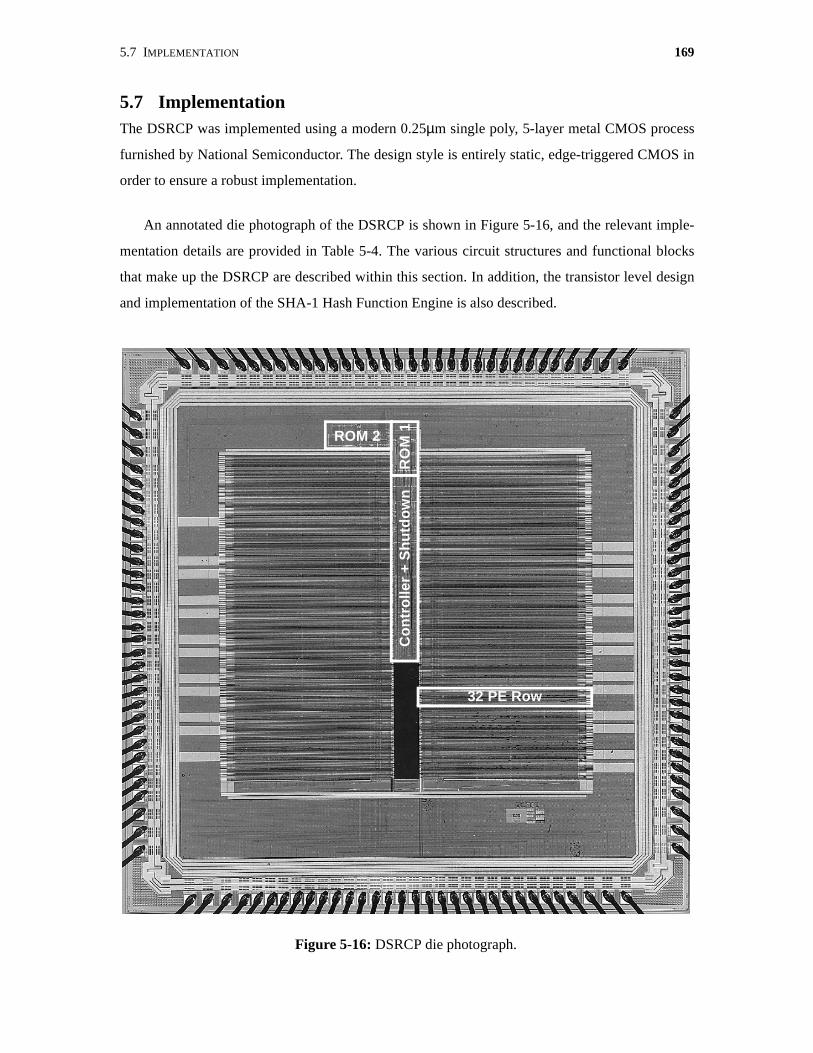
5.7 IMPLEMENTATION 169
5.7 ImplementationThe DSRCP was implemented using a modern 0.25µm single poly, 5-layer metal CMOS process
furnished by National Semiconductor. The design style is entirely static, edge-triggered CMOS in
order to ensure a robust implementation.
An annotated die photograph of the DSRCP is shown in Figure 5-16, and the relevant imple-
mentation details are provided in Table 5-4. The various circuit structures and functional blocks
that make up the DSRCP are described within this section. In addition, the transistor level design
and implementation of the SHA-1 Hash Function Engine is also described.
Figure 5-16: DSRCP die photograph.
32 PE Row
Co
ntr
olle
r +
Sh
utd
ow
n
ROM 2
RO
M 1
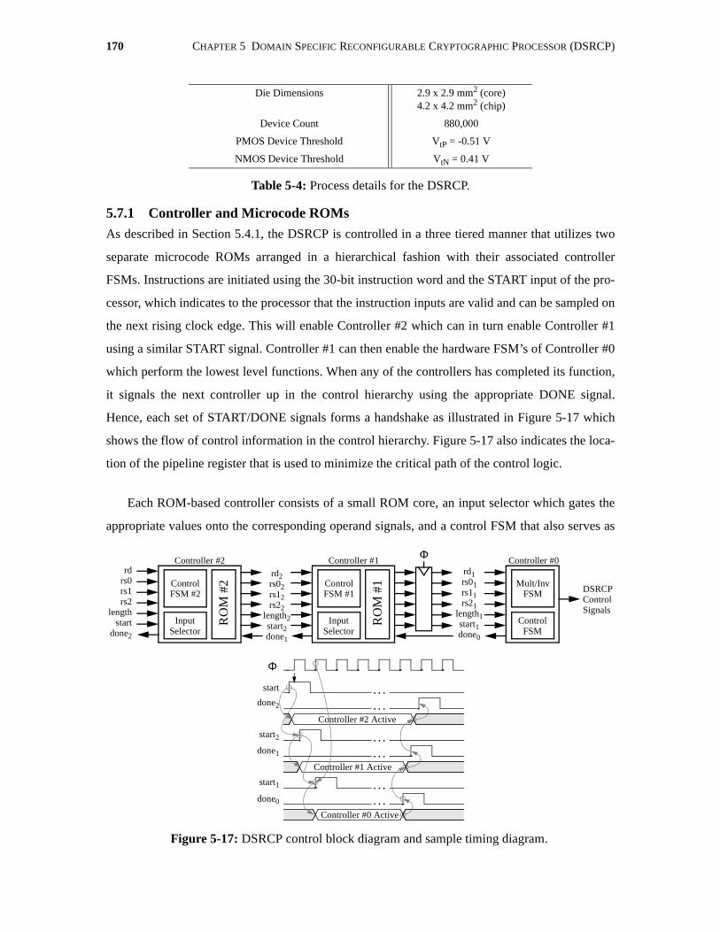
170 CHAPTER 5 DOMAIN SPECIFIC RECONFIGURABLE CRYPTOGRAPHIC PROCESSOR (DSRCP)
5.7.1 Controller and Microcode ROMsAs described in Section 5.4.1, the DSRCP is controlled in a three tiered manner that utilizes two
separate microcode ROMs arranged in a hierarchical fashion with their associated controller
FSMs. Instructions are initiated using the 30-bit instruction word and the START input of the pro-
cessor, which indicates to the processor that the instruction inputs are valid and can be sampled on
the next rising clock edge. This will enable Controller #2 which can in turn enable Controller #1
using a similar START signal. Controller #1 can then enable the hardware FSM’s of Controller #0
which perform the lowest level functions. When any of the controllers has completed its function,
it signals the next controller up in the control hierarchy using the appropriate DONE signal.
Hence, each set of START/DONE signals forms a handshake as illustrated in Figure 5-17 which
shows the flow of control information in the control hierarchy. Figure 5-17 also indicates the loca-
tion of the pipeline register that is used to minimize the critical path of the control logic.
Each ROM-based controller consists of a small ROM core, an input selector which gates the
appropriate values onto the corresponding operand signals, and a control FSM that also serves as
Die Dimensions 2.9 x 2.9 mm2 (core)4.2 x 4.2 mm2 (chip)
Device Count 880,000
PMOS Device Threshold VtP = -0.51 V
NMOS Device Threshold VtN = 0.41 V
Table 5-4: Process details for the DSRCP.
Figure 5-17: DSRCP control block diagram and sample timing diagram.
RO
M #
2
InputSelector
ControlFSM #2
rdrs0rs1rs2
lengthstart
done2
rd2rs02rs12rs22
length2start2done1
RO
M #
1
InputSelector
ControlFSM #1
Φ
ControlFSM
Mult/InvFSM
rd1rs01rs11rs21
length1start1done0
DSRCPControlSignals
Φ
start
start2
start1
Controller #0 Active
Controller #2 Controller #1 Controller #0
done0
done1
done2
. . .
. . .
. . .Controller #1 Active
. . .Controller #2 Active
. . .
. . .
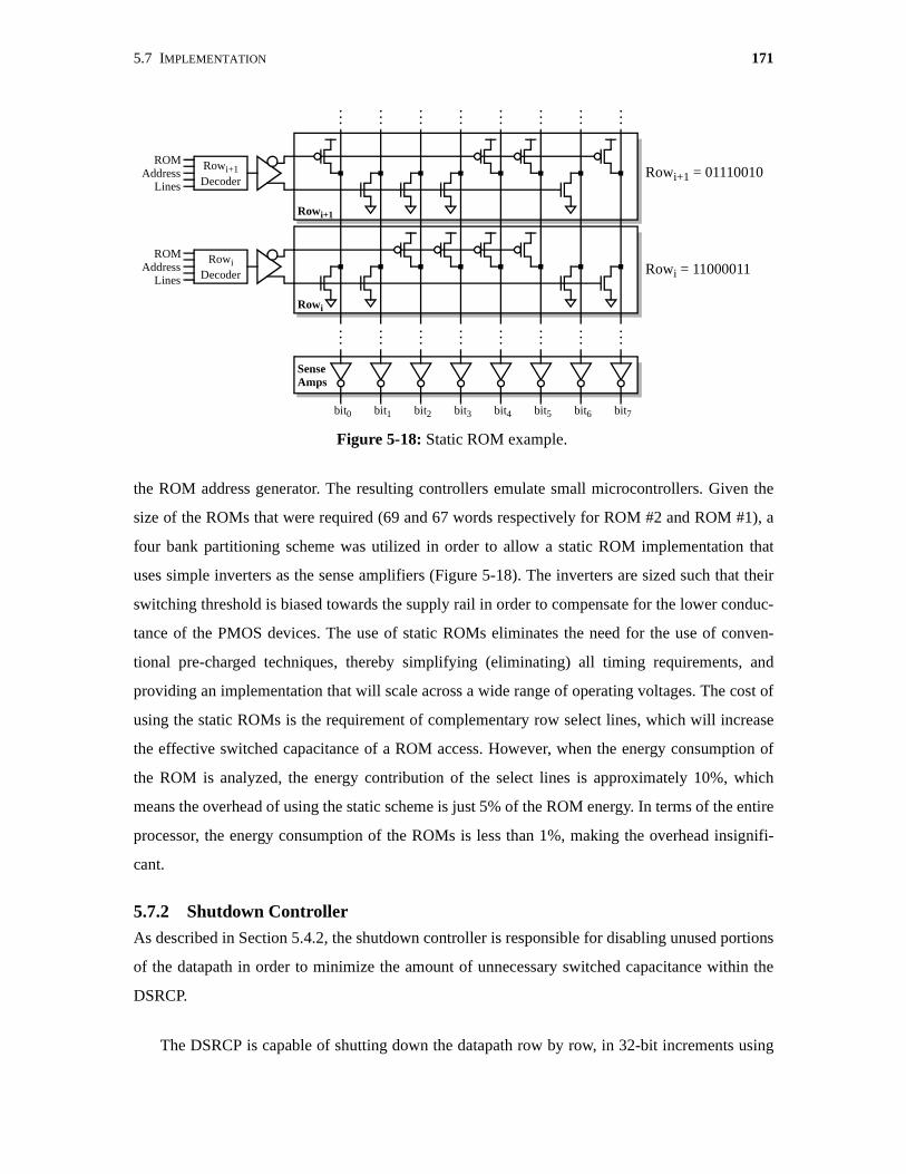
5.7 IMPLEMENTATION 171
the ROM address generator. The resulting controllers emulate small microcontrollers. Given the
size of the ROMs that were required (69 and 67 words respectively for ROM #2 and ROM #1), a
four bank partitioning scheme was utilized in order to allow a static ROM implementation that
uses simple inverters as the sense amplifiers (Figure 5-18). The inverters are sized such that their
switching threshold is biased towards the supply rail in order to compensate for the lower conduc-
tance of the PMOS devices. The use of static ROMs eliminates the need for the use of conven-
tional pre-charged techniques, thereby simplifying (eliminating) all timing requirements, and
providing an implementation that will scale across a wide range of operating voltages. The cost of
using the static ROMs is the requirement of complementary row select lines, which will increase
the effective switched capacitance of a ROM access. However, when the energy consumption of
the ROM is analyzed, the energy contribution of the select lines is approximately 10%, which
means the overhead of using the static scheme is just 5% of the ROM energy. In terms of the entire
processor, the energy consumption of the ROMs is less than 1%, making the overhead insignifi-
cant.
5.7.2 Shutdown Controller
As described in Section 5.4.2, the shutdown controller is responsible for disabling unused portions
of the datapath in order to minimize the amount of unnecessary switched capacitance within the
DSRCP.
The DSRCP is capable of shutting down the datapath row by row, in 32-bit increments using
Figure 5-18: Static ROM example.
Rowi+1
Rowi+1Decoder
ROMAddress
Lines
bit0 bit1 bit2 bit3 bit4 bit5 bit6 bit7
Rowi Contents = 01110010
Rowi
RowiDecoder
ROMAddress
Lines
SenseAmps
. . .
. . .
. . .
. . .
. . .
. . .
. . .
. . .
. . .
. . .
. . .
. . .
. . .
. . .
. . .
. . .
Rowi+1 = 01110010
Rowi = 11000011

172 CHAPTER 5 DOMAIN SPECIFIC RECONFIGURABLE CRYPTOGRAPHIC PROCESSOR (DSRCP)
both clock and control signal gating which is performed in the row drivers that are found along the
inside edge of the two halves of the datapath, as shown in Figure 5-19. The gating is performed
using simple AND structures. The gating signal is generated off the falling edge of the main clock
to ensure that edge-triggered signals generated from the main clock (e.g., the register file clocks)
are gated during the low phase of the clock to eliminate any spurious glitches that might occur by
ANDing the clock with a late-arriving enable signal while the clock is high.
5.7.3 I/O Interface
Operands used within the processor can vary in size from 8-1024 bits (1025 bits in the case of field
polynomials), requiring the use of a flexible I/O interface that allows the user to transfer data to/
from the processor in a very efficient manner. The processor’s floorplan is based on two banks of
processing elements. Each bank contains 16 rows, with 32 processing elements per row. This clus-
tering of 32 PE’s per row maps ideally to a very efficient 32-bit interface that requires at most 32
cycles to load or unload a 1024-bit operand. This arrangement also allows the use of vertical bus-
sing for the distribution of I/O data, which minimizes the area overhead required as few signals are
run vertically. Thus, there is an abundance of routing space. In addition, by using a shared bus
scheme, only two wires per bitslice, 64 wires in all, are required (32 for input and 32 for output). In
comparison, were the I/O data to be distributed horizontally, it would require 32 wires per row for
a single-cycle, full parallel distribution. Given that all of the horizontal routing resources are
already allocated for control signal distribution, the required routing resources would need addi-
tional area. Of course, one can always trade off speed for area by using multiple-cycle, time-multi-
plexed data distribution on fewer wires.
Figure 5-19: Shutdown strategy in the DSRCP.
row 0
row 15
row 31
row 16
Con
trol
Sign
als
Shu
tdow
nC
ontr
ol
ControlSignals
rowEnable3
row drivers
rowEnable3
controligatedControli
row 3
. . . 32-bit
Row of ProcessingElements
. . .
row driver

5.7 IMPLEMENTATION 173
The decision to utilize two separate busses for input and output enables static bus repeaters/
latches to be inserted into the busses at the vertical midpoint of the two banks, allowing the busses
to be segmented in order to minimize the capacitive load seen by any given driver on the bus. This
allows minimum-sized drivers to be used and eliminates the unnecessary charging/discharging of
large portions of the bus capacitance by near-end drivers (e.g., rows 8-15 and 16-23). The final
input/output bus architecture is demonstrated in Figure 5-20.
Operands within the datapath are distributed among the PEs as shown in Figure 5-21. The LSB
en_inD en_inA
en_inBen_inC
Figure 5-20: I/O bussing architectures used within the DSRCP.
. . .. . .
. . .
. . .
io_outrow0
io_outrow7
io_outrow8
io_outrow15
io_outrow31
io_outrow24
io_outrow23
io_outrow16
en_out0
en_out7
en_out8
en_out15
en_out31
en_out24
en_out23
en_out16
en_outD en_outA
en_outBen_outC
io_out<31:0>
. . .. . .
. . .
. . .
io_inrow0
io_inrow7
io_inrow8
io_inrow15
io_inrow31
io_inrow24
io_inrow23
io_inrow16
en_in0
en_in7
en_in8
en_in15
en_in31
en_in24
en_in23
en_in16
io_in<31:0>
Figure 5-21: Direction of operand flow within the DSRCP datapath.
0 31
3263
64
1023992
991 960
959
511 480
479448
447
512543
544 575
576
. . .
. . .. . .
. . .
174 CHAPTER 5 DOMAIN SPECIFIC RECONFIGURABLE CRYPTOGRAPHIC PROCESSOR (DSRCP)
is stored in the leftmost PE of the first row of the right bank, and the MSB is stored in rightmost
element of the top row in the left bank. As a result, when data is read in/out vertically, every other
row is reversed in terms of its bit-order, requiring the use of a multiplexor-based swapping unit to
ensure a consistent bit-ordering. This re-ordering can be done directly at the processor’s interface
to enable a very compact layout, and can be controlled using the interface logic that generates the
row enable signals for the I/O interface.
5.7.4 Reconfigurable Datapath BitsliceThe reconfigurable datapath bitslice represents the main circuit element of the DSRCP both in
terms of functionality and area resources. The bitslice consists of five distinct components: an 8-
word register file, I/O interface, fast comparator, fast adder, and the reconfigurable datapath cir-
cuitry with local storage. The bitslice architecture is shown in Figure 5-22.
The physical layout of the bitslice is shown in Figure 5-23 along with a block diagram depict-
ing the mapping of the various circuit elements within the bitslice. The map is required due to the
density of the final layout which makes it difficult to identify individual circuit features. The den-
sity of the layout is much improved over that of the ESEP (Figure 4-17) due to the abundancy of
metal layers which allow for over-cell routing, leading to a very dense final layout that is approxi-
mately µm2. As in the ESEP, the layout was designed such that all inter-cell connections
are made via abutment of the layout in both the horizontal (for all control signals) and vertical (for
I/O bussing) directions.
30 150×

5.7 IMPLEMENTATION 175
Figure 5-22: DSRCP bitslice architecture.
I/O Interface
CLEARREG7:0
CLKREG7:0
R0SEL2:0
R1SEL2:0
CMPSELA1:0
CMPSELB1:0
ADDSELA1:0
ADDSELB1:0
SUB
CARRY
Pi-1
Gi-1
SUMi
RSHIFT
CLKSUM
CLRSUM
IOSEL
REGSEL5:0
ADDSEL2:0
Ai
Bi
Bi-1
PCi
PSi
PCi-1
XCi-1
XSi
YCi
YSi
qj
bj
CLKREG5:0
CLRREG5:0
Comparator
Adder
Register File
ReconfigurableDatapath
CLKIO
CLRIO
REGSEL5:0
ADDSEL2:0
Ai+1
Bi+1
Bi
PCi+1
PSi+1
PCi
XCi
XSi+1
YCi+1
YSi+1
qj
bj
CLKREG5:0
CLRREG5:0
PC
i-1
RS0
i
WB
iN
iP
Ci
PS
i
IOO
UT
iIO
INi
PC
i-1
RS0 i
WB
iN
iP
Ci
PS
i
IOO
UT
iIO
INi
RS0
i
WB
iN
iP
Ci
PS
i
IOO
UT
iIO
INi
RS1
i
RE
GS
UM
i
RS0
i
WB
i
IOO
UT
iIO
INi
RS1
i
RE
GS
UM
i
RS1 i
RS0 i
WB
iN
iP
Ci
PS
i
IOO
UT
iIO
INi
IOO
UT
i
IOIN
i
IOOUTi IOINi
RS1 i
RS0 i
WB
i
IOO
UT
iIO
INi
IOO
UT
iIO
INi
IOO
UT
iIO
INi
IOO
UT
i
IOIN
i
ADDSELA1:0
ADDSELB1:0
SUB
CARRY
Pi
Gi
SUMi+1
RSHIFT
CLKSUM
CLRSUM
CMPSELA1:0
CMPSELB1:0
GTi
EQi
CLEARREG7:0
CLKREG7:0
R0SEL2:0
R1SEL2:0
IOSEL
CLKIO
CLRIO
IOOUTi IOINi
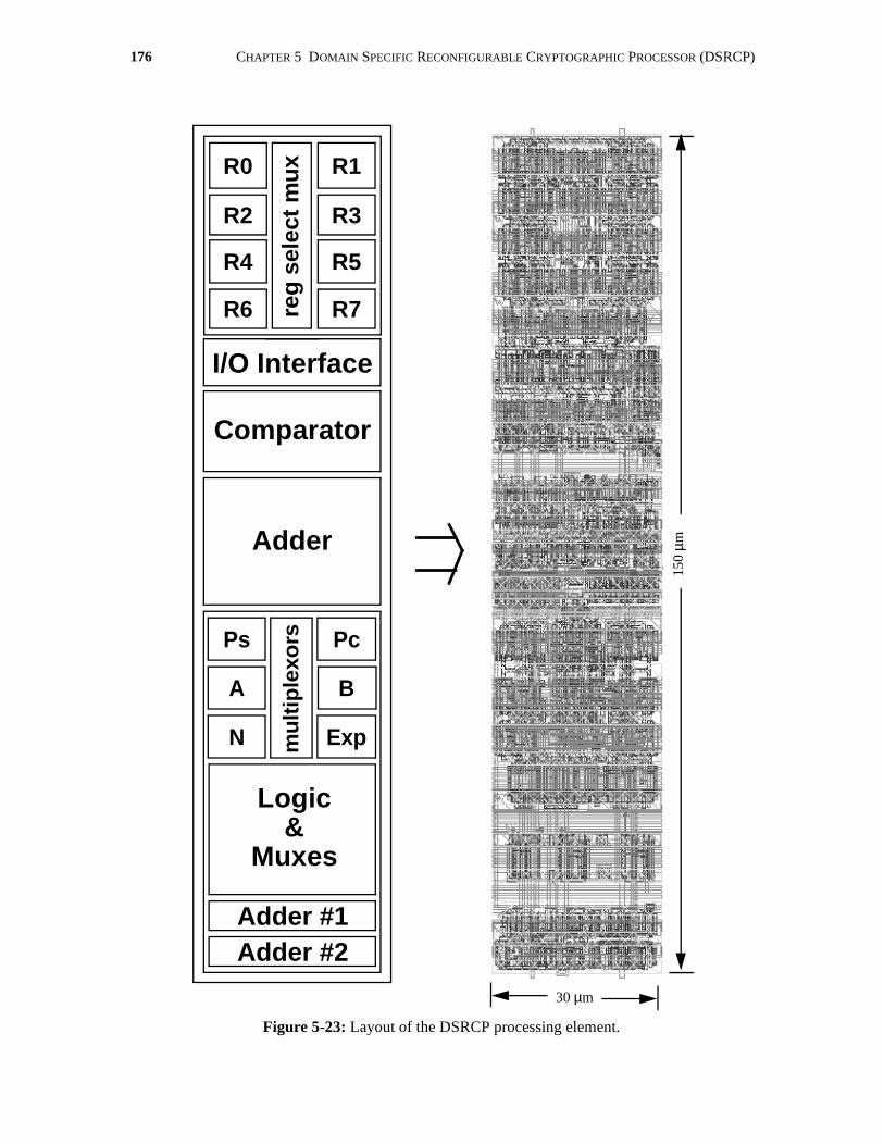
176 CHAPTER 5 DOMAIN SPECIFIC RECONFIGURABLE CRYPTOGRAPHIC PROCESSOR (DSRCP)
Figure 5-23: Layout of the DSRCP processing element.
150
µm
30 µm
Ps
A
N
Pc
B
Expmu
ltip
lexo
rs
Logic&
Muxes
Adder #1Adder #2
R0
R2
R4
R6
R1
R3
R5
R7reg
sel
ect
mu
x
I/O Interface
Adder
Comparator
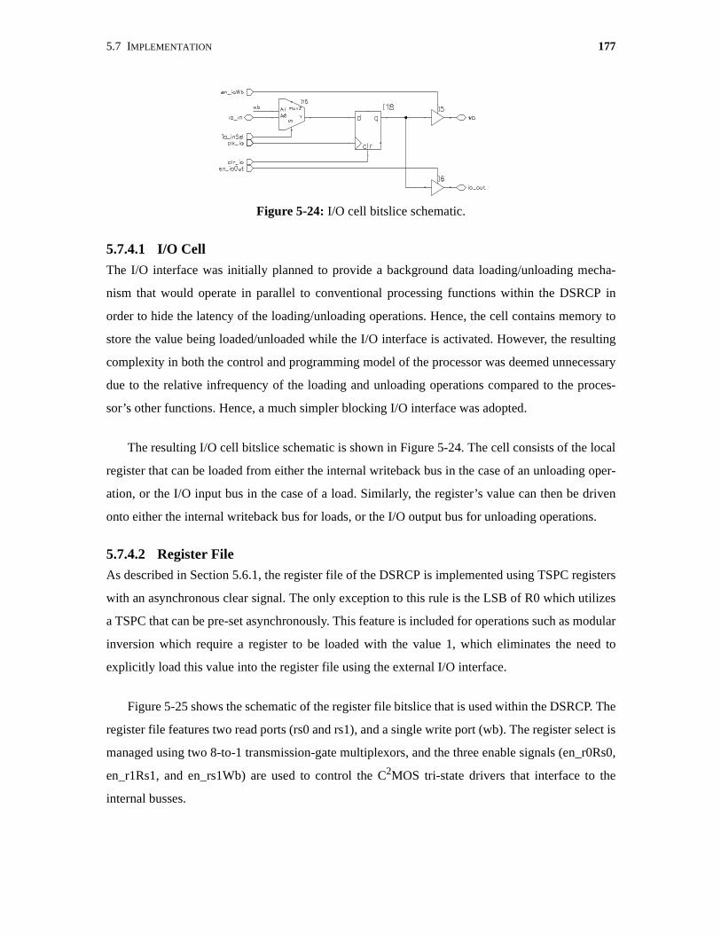
5.7 IMPLEMENTATION 177
5.7.4.1 I/O Cell
The I/O interface was initially planned to provide a background data loading/unloading mecha-
nism that would operate in parallel to conventional processing functions within the DSRCP in
order to hide the latency of the loading/unloading operations. Hence, the cell contains memory to
store the value being loaded/unloaded while the I/O interface is activated. However, the resulting
complexity in both the control and programming model of the processor was deemed unnecessary
due to the relative infrequency of the loading and unloading operations compared to the proces-
sor’s other functions. Hence, a much simpler blocking I/O interface was adopted.
The resulting I/O cell bitslice schematic is shown in Figure 5-24. The cell consists of the local
register that can be loaded from either the internal writeback bus in the case of an unloading oper-
ation, or the I/O input bus in the case of a load. Similarly, the register’s value can then be driven
onto either the internal writeback bus for loads, or the I/O output bus for unloading operations.
5.7.4.2 Register FileAs described in Section 5.6.1, the register file of the DSRCP is implemented using TSPC registers
with an asynchronous clear signal. The only exception to this rule is the LSB of R0 which utilizes
a TSPC that can be pre-set asynchronously. This feature is included for operations such as modular
inversion which require a register to be loaded with the value 1, which eliminates the need to
explicitly load this value into the register file using the external I/O interface.
Figure 5-25 shows the schematic of the register file bitslice that is used within the DSRCP. The
register file features two read ports (rs0 and rs1), and a single write port (wb). The register select is
managed using two 8-to-1 transmission-gate multiplexors, and the three enable signals (en_r0Rs0,
en_r1Rs1, and en_rs1Wb) are used to control the C2MOS tri-state drivers that interface to the
internal busses.
Figure 5-24: I/O cell bitslice schematic.
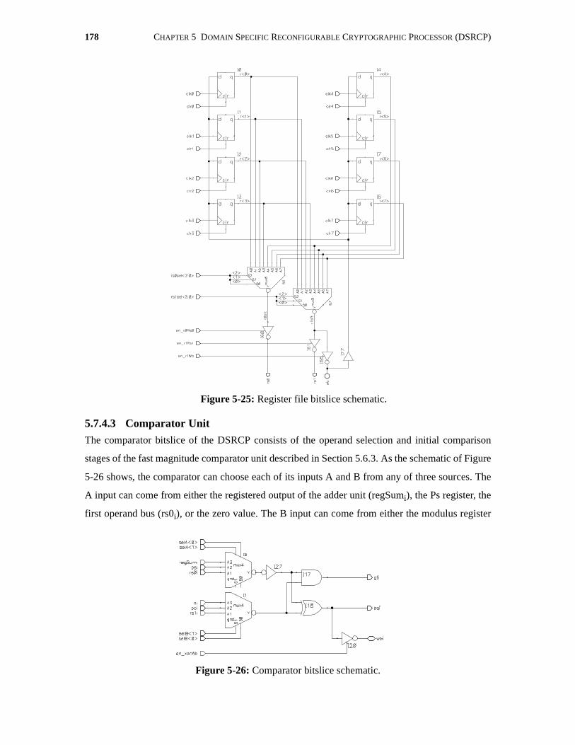
178 CHAPTER 5 DOMAIN SPECIFIC RECONFIGURABLE CRYPTOGRAPHIC PROCESSOR (DSRCP)
5.7.4.3 Comparator Unit
The comparator bitslice of the DSRCP consists of the operand selection and initial comparison
stages of the fast magnitude comparator unit described in Section 5.6.3. As the schematic of Figure
5-26 shows, the comparator can choose each of its inputs A and B from any of three sources. The
A input can come from either the registered output of the adder unit (regSumi), the Ps register, the
first operand bus (rs0i), or the zero value. The B input can come from either the modulus register
Figure 5-25: Register file bitslice schematic.
Figure 5-26: Comparator bitslice schematic.
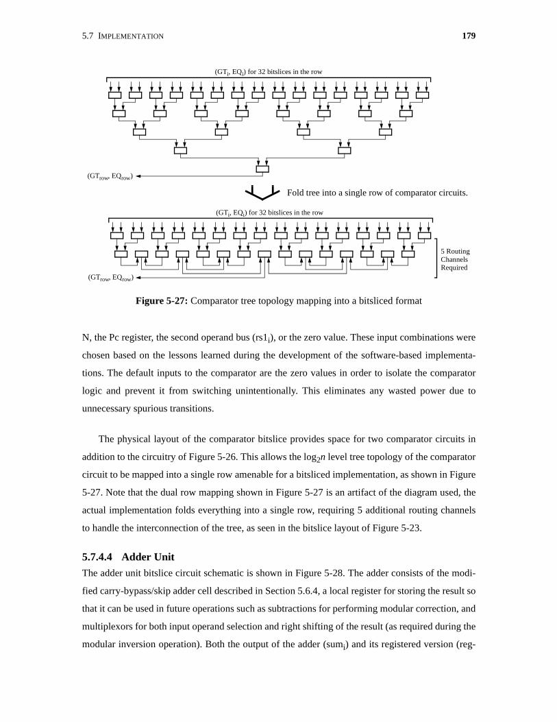
5.7 IMPLEMENTATION 179
N, the Pc register, the second operand bus (rs1i), or the zero value. These input combinations were
chosen based on the lessons learned during the development of the software-based implementa-
tions. The default inputs to the comparator are the zero values in order to isolate the comparator
logic and prevent it from switching unintentionally. This eliminates any wasted power due to
unnecessary spurious transitions.
The physical layout of the comparator bitslice provides space for two comparator circuits in
addition to the circuitry of Figure 5-26. This allows the log2n level tree topology of the comparator
circuit to be mapped into a single row amenable for a bitsliced implementation, as shown in Figure
5-27. Note that the dual row mapping shown in Figure 5-27 is an artifact of the diagram used, the
actual implementation folds everything into a single row, requiring 5 additional routing channels
to handle the interconnection of the tree, as seen in the bitslice layout of Figure 5-23.
5.7.4.4 Adder UnitThe adder unit bitslice circuit schematic is shown in Figure 5-28. The adder consists of the modi-
fied carry-bypass/skip adder cell described in Section 5.6.4, a local register for storing the result so
that it can be used in future operations such as subtractions for performing modular correction, and
multiplexors for both input operand selection and right shifting of the result (as required during the
modular inversion operation). Both the output of the adder (sumi) and its registered version (reg-
Figure 5-27: Comparator tree topology mapping into a bitsliced format
5 RoutingChannels
(GTrow, EQrow)
(GTrow, EQrow)
(GTi, EQi) for 32 bitslices in the row
Required
(GTi, EQi) for 32 bitslices in the row
Fold tree into a single row of comparator circuits.
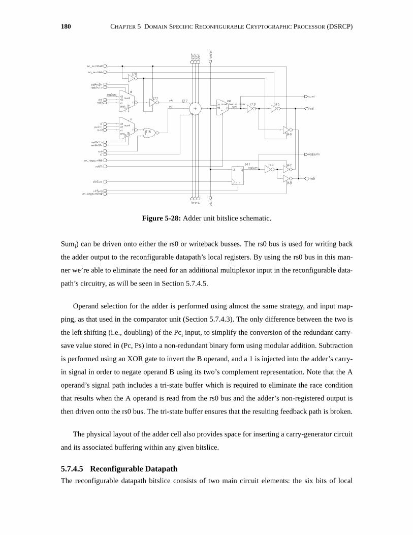
180 CHAPTER 5 DOMAIN SPECIFIC RECONFIGURABLE CRYPTOGRAPHIC PROCESSOR (DSRCP)
Sumi) can be driven onto either the rs0 or writeback busses. The rs0 bus is used for writing back
the adder output to the reconfigurable datapath’s local registers. By using the rs0 bus in this man-
ner we’re able to eliminate the need for an additional multiplexor input in the reconfigurable data-
path’s circuitry, as will be seen in Section 5.7.4.5.
Operand selection for the adder is performed using almost the same strategy, and input map-
ping, as that used in the comparator unit (Section 5.7.4.3). The only difference between the two is
the left shifting (i.e., doubling) of the Pci input, to simplify the conversion of the redundant carry-
save value stored in (Pc, Ps) into a non-redundant binary form using modular addition. Subtraction
is performed using an XOR gate to invert the B operand, and a 1 is injected into the adder’s carry-
in signal in order to negate operand B using its two’s complement representation. Note that the A
operand’s signal path includes a tri-state buffer which is required to eliminate the race condition
that results when the A operand is read from the rs0 bus and the adder’s non-registered output is
then driven onto the rs0 bus. The tri-state buffer ensures that the resulting feedback path is broken.
The physical layout of the adder cell also provides space for inserting a carry-generator circuit
and its associated buffering within any given bitslice.
5.7.4.5 Reconfigurable DatapathThe reconfigurable datapath bitslice consists of two main circuit elements: the six bits of local
Figure 5-28: Adder unit bitslice schematic.

5.7 IMPLEMENTATION 181
storage for the Pc, Ps, A, B, N, and EXP registers, and the reconfigurable adder/AND circuits that
implement the various functions described in Section 5.6.5. The resulting circuit implementation is
shown in Figure 5-29. The registers used for local storage are implemented with the same TSPC
style used within the register file. The reconfigurable adder cells are implemented using area-effi-
cient transmission-gate adder cells, whose schematic is shown in Figure 5-30.
In addition to these circuit elements, the reconfigurable datapath requires two n-bit and two
-bit multiplexors which are implemented using the folding technique described in Section
Figure 5-29: Reconfigurable datapath bitslice schematic.
n 2⁄
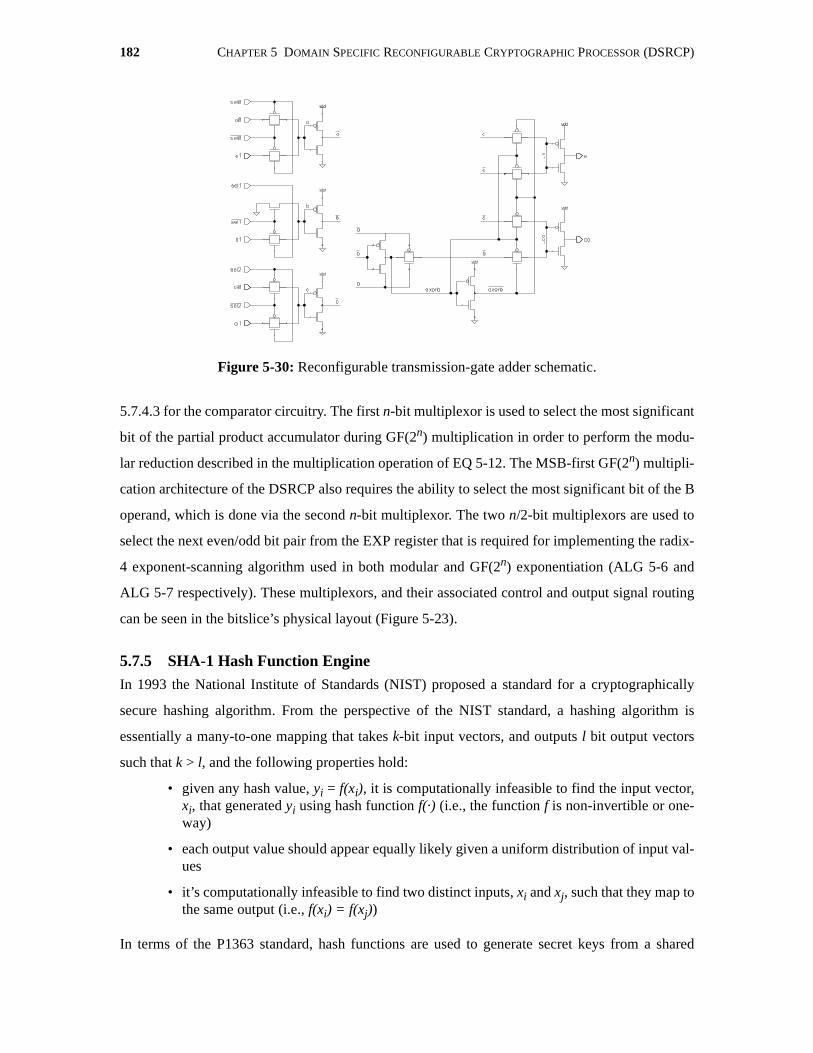
182 CHAPTER 5 DOMAIN SPECIFIC RECONFIGURABLE CRYPTOGRAPHIC PROCESSOR (DSRCP)
5.7.4.3 for the comparator circuitry. The first n-bit multiplexor is used to select the most significant
bit of the partial product accumulator during GF(2n) multiplication in order to perform the modu-
lar reduction described in the multiplication operation of EQ 5-12. The MSB-first GF(2n) multipli-
cation architecture of the DSRCP also requires the ability to select the most significant bit of the B
operand, which is done via the second n-bit multiplexor. The two n/2-bit multiplexors are used to
select the next even/odd bit pair from the EXP register that is required for implementing the radix-
4 exponent-scanning algorithm used in both modular and GF(2n) exponentiation (ALG 5-6 and
ALG 5-7 respectively). These multiplexors, and their associated control and output signal routing
can be seen in the bitslice’s physical layout (Figure 5-23).
5.7.5 SHA-1 Hash Function EngineIn 1993 the National Institute of Standards (NIST) proposed a standard for a cryptographically
secure hashing algorithm. From the perspective of the NIST standard, a hashing algorithm is
essentially a many-to-one mapping that takes k-bit input vectors, and outputs l bit output vectors
such that k > l, and the following properties hold:
• given any hash value, yi = f(xi), it is computationally infeasible to find the input vector,xi, that generated yi using hash function f(·) (i.e., the function f is non-invertible or one-way)
• each output value should appear equally likely given a uniform distribution of input val-ues
• it’s computationally infeasible to find two distinct inputs, xi and xj, such that they map tothe same output (i.e., f(xi) = f(xj))
In terms of the P1363 standard, hash functions are used to generate secret keys from a shared
Figure 5-30: Reconfigurable transmission-gate adder schematic.
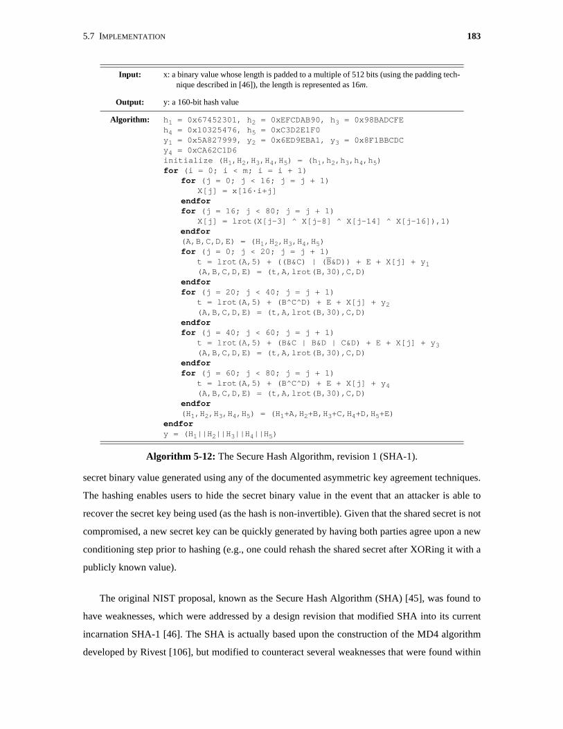
5.7 IMPLEMENTATION 183
secret binary value generated using any of the documented asymmetric key agreement techniques.
The hashing enables users to hide the secret binary value in the event that an attacker is able to
recover the secret key being used (as the hash is non-invertible). Given that the shared secret is not
compromised, a new secret key can be quickly generated by having both parties agree upon a new
conditioning step prior to hashing (e.g., one could rehash the shared secret after XORing it with a
publicly known value).
The original NIST proposal, known as the Secure Hash Algorithm (SHA) [45], was found to
have weaknesses, which were addressed by a design revision that modified SHA into its current
incarnation SHA-1 [46]. The SHA is actually based upon the construction of the MD4 algorithm
developed by Rivest [106], but modified to counteract several weaknesses that were found within
Input: x: a binary value whose length is padded to a multiple of 512 bits (using the padding tech-nique described in [46]), the length is represented as 16m.
Output: y: a 160-bit hash value
Algorithm: h1 = 0x67452301, h2 = 0xEFCDAB90, h3 = 0x98BADCFEh4 = 0x10325476, h5 = 0xC3D2E1F0y1 = 0x5A827999, y2 = 0x6ED9EBA1, y3 = 0x8F1BBCDCy4 = 0xCA62C1D6initialize (H1,H2,H3,H4,H5) = (h1,h2,h3,h4,h5)for (i = 0; i < m; i = i + 1)
for (j = 0; j < 16; j = j + 1)X[j] = x[16·i+j]
endforfor (j = 16; j < 80; j = j + 1)
X[j] = lrot(X[j-3] ^ X[j-8] ^ X[j-14] ^ X[j-16]),1)endfor(A,B,C,D,E) = (H1,H2,H3,H4,H5)for (j = 0; j < 20; j = j + 1)
t = lrot(A,5) + ((B&C) | (B&D)) + E + X[j] + y1(A,B,C,D,E) = (t,A,lrot(B,30),C,D)
endforfor (j = 20; j < 40; j = j + 1)
t = lrot(A,5) + (B^C^D) + E + X[j] + y2(A,B,C,D,E) = (t,A,lrot(B,30),C,D)
endforfor (j = 40; j < 60; j = j + 1)
t = lrot(A,5) + (B&C | B&D | C&D) + E + X[j] + y3(A,B,C,D,E) = (t,A,lrot(B,30),C,D)
endforfor (j = 60; j < 80; j = j + 1)
t = lrot(A,5) + (B^C^D) + E + X[j] + y4(A,B,C,D,E) = (t,A,lrot(B,30),C,D)
endfor(H1,H2,H3,H4,H5) = (H1+A,H2+B,H3+C,H4+D,H5+E)
endfory = (H1||H2||H3||H4||H5)
Algorithm 5-12: The Secure Hash Algorithm, revision 1 (SHA-1).

184 CHAPTER 5 DOMAIN SPECIFIC RECONFIGURABLE CRYPTOGRAPHIC PROCESSOR (DSRCP)
MD4, as well as to provide additional measures to increase its lifetime (e.g., using 160 bit chaining
values, as opposed to MD4’s 128 bit values).
The SHA-1 algorithm is given in ALG 5-12, where lrot(x,y) is the left rotation of the vec-
tor x by y bit positions, || is the concatenation operation, and all additions are assumed to be mod-
ulo-232
ALG 5-12 is implemented using the circuit shown in Figure 5-31. The Hi reset to their respec-
tive hi values, while the yi values are generated in the control logic. The adders that are used to
update the Hi values are isolated using transmission gates in order to eliminate spurious transitions
in the adders due to the constantly changing chaining variable values (A, B, C, D, and E) which are
updated every round. The 32-bit adders are implemented using the same modified carry-bypass/
skip architecture of Section 5.6.4.
The X[j] values are computed in the 512-bit circular buffer which emulates ALG 5-12’s 80-
word X[j] array using a single 16-word array whose values are updated during each cycle of the
SHA-1 algorithm. The circular buffer is initially loaded during a 16-cycle load phase that preceeds
each 80-cycle computation of the new hash values. Hence, 96 cycles are needed to process each
512-bit input block. Note that this design requires no external memory to process each 512-bit
block, although it does require an external processor to handle the data padding operation in which
an arbitrary length input vector is mapped to a sequence of 512-bit blocks.
Figure 5-31: SHA-1 architecture.
512-bitCircular Buffer
Round Function
H2H1 H4H3 H5
160
A B C D E
Controller
32Data Input
X[j]32
32yi
Hash Output
control
updateHi
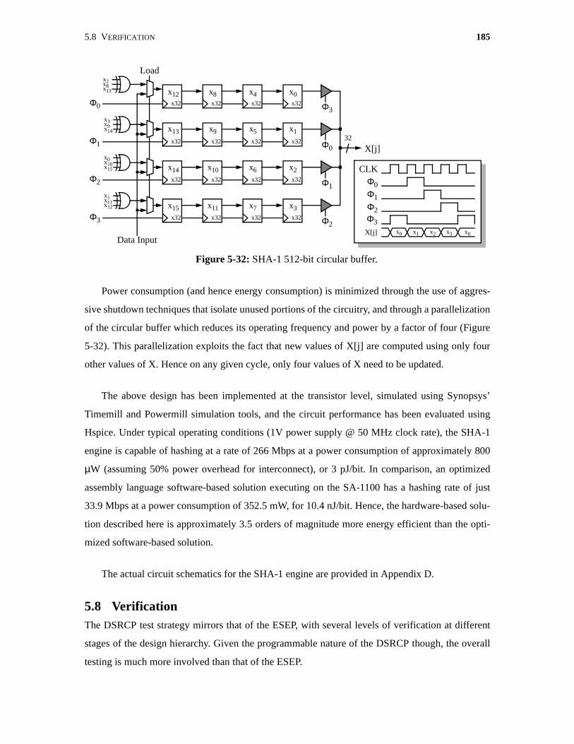
5.8 VERIFICATION 185
Power consumption (and hence energy consumption) is minimized through the use of aggres-
sive shutdown techniques that isolate unused portions of the circuitry, and through a parallelization
of the circular buffer which reduces its operating frequency and power by a factor of four (Figure
5-32). This parallelization exploits the fact that new values of X[j] are computed using only four
other values of X. Hence on any given cycle, only four values of X need to be updated.
The above design has been implemented at the transistor level, simulated using Synopsys’
Timemill and Powermill simulation tools, and the circuit performance has been evaluated using
Hspice. Under typical operating conditions (1V power supply @ 50 MHz clock rate), the SHA-1
engine is capable of hashing at a rate of 266 Mbps at a power consumption of approximately 800
µW (assuming 50% power overhead for interconnect), or 3 pJ/bit. In comparison, an optimized
assembly language software-based solution executing on the SA-1100 has a hashing rate of just
33.9 Mbps at a power consumption of 352.5 mW, for 10.4 nJ/bit. Hence, the hardware-based solu-
tion described here is approximately 3.5 orders of magnitude more energy efficient than the opti-
mized software-based solution.
The actual circuit schematics for the SHA-1 engine are provided in Appendix D.
5.8 VerificationThe DSRCP test strategy mirrors that of the ESEP, with several levels of verification at different
stages of the design hierarchy. Given the programmable nature of the DSRCP though, the overall
testing is much more involved than that of the ESEP.
Figure 5-32: SHA-1 512-bit circular buffer.
x32x32x32x32
x32x32x32x32
x32x32x32x32
x32x32x32x32
Φ3
Φ0
Φ1
Φ2
32
Φ0
Φ1
Φ2
Φ3
X[j]
Φ3
Φ2
Φ1
Φ0
CLK
Data Input
x0x4x8x12
x1x5x9x13
x2x6x10x14
x3x7x11x15
x10x15
x0
x11x12
x1
x9x14
x3
x8x13
x2
Load
X[j]
x0 x1 x2 x3 x0
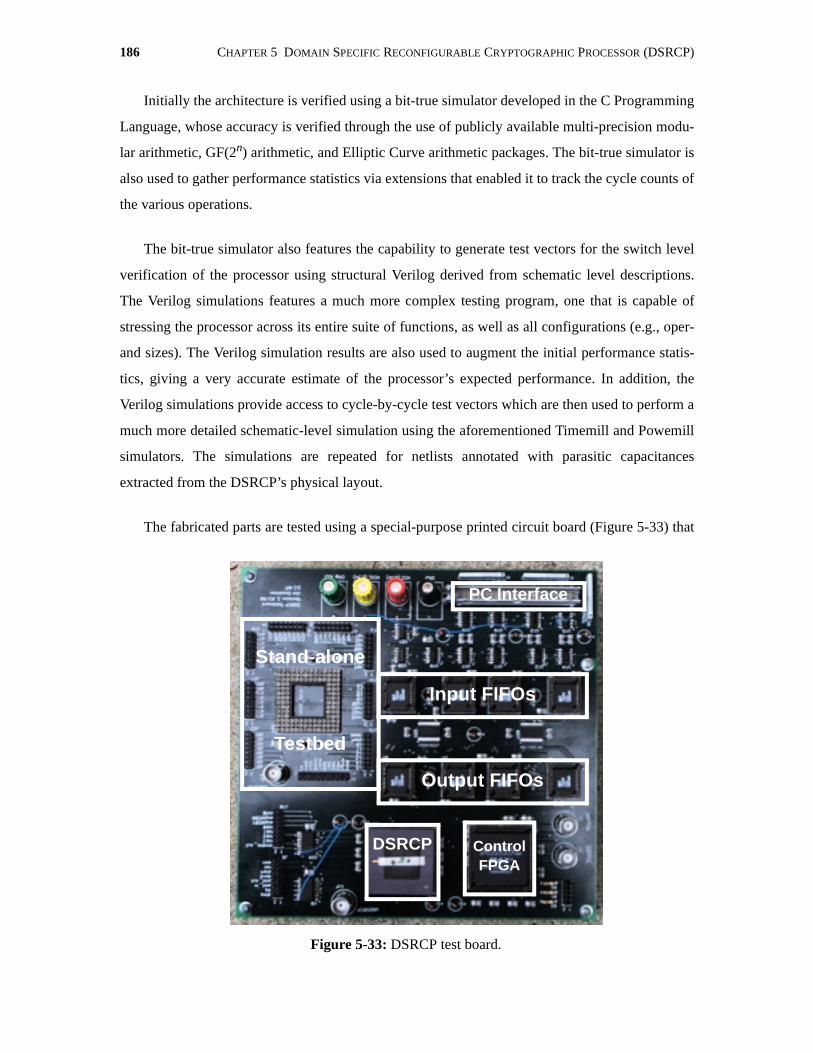
186 CHAPTER 5 DOMAIN SPECIFIC RECONFIGURABLE CRYPTOGRAPHIC PROCESSOR (DSRCP)
Initially the architecture is verified using a bit-true simulator developed in the C Programming
Language, whose accuracy is verified through the use of publicly available multi-precision modu-
lar arithmetic, GF(2n) arithmetic, and Elliptic Curve arithmetic packages. The bit-true simulator is
also used to gather performance statistics via extensions that enabled it to track the cycle counts of
the various operations.
The bit-true simulator also features the capability to generate test vectors for the switch level
verification of the processor using structural Verilog derived from schematic level descriptions.
The Verilog simulations features a much more complex testing program, one that is capable of
stressing the processor across its entire suite of functions, as well as all configurations (e.g., oper-
and sizes). The Verilog simulation results are also used to augment the initial performance statis-
tics, giving a very accurate estimate of the processor’s expected performance. In addition, the
Verilog simulations provide access to cycle-by-cycle test vectors which are then used to perform a
much more detailed schematic-level simulation using the aforementioned Timemill and Powemill
simulators. The simulations are repeated for netlists annotated with parasitic capacitances
extracted from the DSRCP’s physical layout.
The fabricated parts are tested using a special-purpose printed circuit board (Figure 5-33) that
Figure 5-33: DSRCP test board.
Stand-alone
Testbed
Input FIFOs
Output FIFOs
ControlFPGA
DSRCP
PC Interface
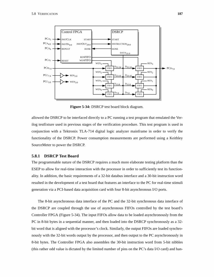
5.8 VERIFICATION 187
allowed the DSRCP to be interfaced directly to a PC running a test program that emulated the Ver-
ilog testfixture used in previous stages of the verification procedure. This test program is used in
conjunction with a Tektronix TLA-714 digital logic analyzer mainframe in order to verify the
functionality of the DSRCP. Power consumption measurements are performed using a Keithley
SourceMeter to power the DSRCP.
5.8.1 DSRCP Test BoardThe programmable nature of the DSRCP requires a much more elaborate testing platform than the
ESEP to allow for real-time interaction with the processor in order to sufficiently test its function-
ality. In addition, the basic requirements of a 32-bit databus interface and a 30-bit instruction word
resulted in the development of a test board that features an interface to the PC for real-time stimuli
generation via a PCI-based data acquisition card with four 8-bit asynchronous I/O ports.
The 8-bit asynchronous data interface of the PC and the 32-bit synchronous data interface of
the DSRCP are coupled through the use of asynchronous FIFOs controlled by the test board’s
Controller FPGA (Figure 5-34). The input FIFOs allow data to be loaded asynchronously from the
PC in 8-bit bytes in a sequential manner, and then loaded into the DSRCP synchronously as a 32-
bit word that is aligned with the processor’s clock. Similarly, the output FIFOs are loaded synchro-
nously with the 32-bit words output by the processor, and then output to the PC asynchronously in
8-bit bytes. The Controller FPGA also assembles the 30-bit instruction word from 5-bit nibbles
(this rather odd value is dictated by the limited number of pins on the PC’s data I/O card) and han-
Figure 5-34: DSRCP test board block diagram.
DSRCP
INSTRUCTION29:0
DATA31:0
START
Control FPGA
DONE
INSTOUT29:0
START
DONE
FIFOD31:24
D23:16
D15:8
D7:0
FIFO
FIFO
FIFO
D31:24
D23:16
D15:8
D7:0
FIFO
FIFO
FIFO
FIFO
REN3
REN2
REN1
REN0
WEN3
WEN2
WEN1
WEN0
WENFIFORENFIFO
INSTIN4:0
INSTCLK
REPEAT
PCA5
PCA4:0
PCA6
RESETPCA7
PCB7:0
PCC7:4
PCC3:0
REN3:0
WEN3:0
PCD7:0
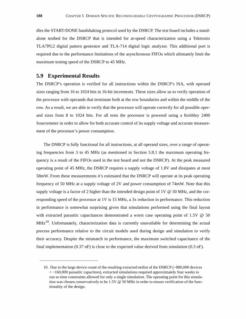
188 CHAPTER 5 DOMAIN SPECIFIC RECONFIGURABLE CRYPTOGRAPHIC PROCESSOR (DSRCP)
dles the START/DONE handshaking protocol used by the DSRCP. The test board includes a stand-
alone testbed for the DSRCP that is intended for at-speed characterization using a Tektronix
TLA7PG2 digital pattern generator and TLA-714 digital logic analyzer. This additional port is
required due to the performance limitations of the asynchronous FIFOs which ultimately limit the
maximum testing speed of the DSRCP to 45 MHz.
5.9 Experimental ResultsThe DSRCP’s operation is verified for all instructions within the DSRCP’s ISA, with operand
sizes ranging from 16 to 1024 bits in 16-bit increments. These sizes allow us to verify operation of
the processor with operands that terminate both at the row boundaries and within the middle of the
row. As a result, we are able to verify that the processor will operate correctly for all possible oper-
and sizes from 8 to 1024 bits. For all tests the processor is powered using a Keithley 2400
Sourcemeter in order to allow for both accurate control of its supply voltage and accurate measure-
ment of the processor’s power consumption.
The DSRCP is fully functional for all instructions, at all operand sizes, over a range of operat-
ing frequencies from 3 to 45 MHz (as mentioned in Section 5.8.1 the maximum operating fre-
quency is a result of the FIFOs used in the test board and not the DSRCP). At the peak measured
operating point of 45 MHz, the DSRCP requires a supply voltage of 1.8V and dissipates at most
58mW. From these measurements it’s estimated that the DSRCP will operate at its peak operating
frequency of 50 MHz at a supply voltage of 2V and power consumption of 74mW. Note that this
supply voltage is a factor of 2 higher than the intended design point of 1V @ 50 MHz, and the cor-
responding speed of the processor at 1V is 15 MHz, a 3x reduction in performance. This reduction
in performance is somewhat surprising given that simulations performed using the final layout
with extracted parasitic capacitances demonstrated a worst case operating point of 1.5V @ 50
MHz10. Unfortunately, characterization data is currently unavailable for determining the actual
process performance relative to the circuit models used during design and simulation to verify
their accuracy. Despite the mismatch in performance, the maximum switched capacitance of the
final implementation (0.37 nF) is close to the expected value derived from simulation (0.3 nF).
10. Due to the large device count of the resulting extracted netlist of the DSRCP (~880,000 devices + ~160,000 parasitic capacitors), extracted simulations required approximately four weeks to run so time constraints allowed for only a single simulation. The operating point for this simula-tion was chosen conservatively to be 1.5V @ 50 MHz in order to ensure verification of the func-tionality of the design.
5.9 EXPERIMENTAL RESULTS 189
The minimum operating voltage of the DSRCP is 0.68V, which is achieved at clock rates up to
3 MHz and a peak power consumption of 525µW. This minimum voltage is dictated by the mini-
mum operating voltage of the level-shifting circuitry used within the DSRCP to interface the lower
core voltage to the 2.5V interface voltage used on the test board.
Table 5-5 shows the performance of the DSRCP instructions whose performance is indepen-
dent of the operand size (with the exception of REG_LOAD and REG_UNLOAD of course). Fig-
ure 5-35 shows the performance of those DSRCP instructions whose execution time is
proportional to the size of the operands. The results are normalized relative to the operand size in
order to better illustrate this proportionality. The resulting performance is as predicted in the ear-
lier design discussions of Section 5.5. The performance of the cryptographic primitives required
for IF, DL, and EC-based cryptography are shown in Figure 5-36. Several important performance
points are highlighted for easy comparison with other reported implementations in Table 5-6. The
DSRCP’s performance compares quite favourably; although several solutions quote higher rates,
they represent dedicated solutions which cannot perform any other functions. From a power con-
Operation Cycle Counts
REG_LOAD, REG_UNLOAD 2 - 32
REG_MOVE, REG_CLEAR 2
ADD/SUB 4
MOD_ADD, MOD_SUB 4 - 10
COMP, GF_ADD 2
Table 5-5: Performance of utility instructions within the DSRCP.
Figure 5-35: Performance of several DSRCP instructions.
Operand Size (bits)
Cyc
les
per
bit
0 256 512 768 10240
2
4
6
8
EC_ADD/DOUBLE
GF_INV/INVMULT
MOD, MOD_MULT
GF_MULT, MONT_REDUCE
~5.5 cycles/bit
~3.3 cycles/bit
~2 cycles/bit
~1 cycles/bit
MOD_INV (not shown, ~14.5)
MONT_REDUCE_A, MONT_MULT

190 CHAPTER 5 DOMAIN SPECIFIC RECONFIGURABLE CRYPTOGRAPHIC PROCESSOR (DSRCP)
sumption perspective, our solution represents a significant reduction in power consumption com-
pared to previous solutions whose power consumption was reported.
Unfortunately, as mentioned in Section 1.2.4, there are few reported implementations of ellip-
tic curve and GF(2n) cryptographic hardware that can be used for comparison. However, for those
that have been reported, the DSRCP performs much better in terms of the time required to perform
DesignPower
Consumption(W)
Operand Size
(bits)
Time per Operation
(ms)
Cycles per Operation(Mcycles)
Clock Rate
(MHz)
Ishii [57] 2W 1024/512 100/25 - 40
Ivey [59] - 512 < 8 - 150
Orup [95] - 512 5 0.125 25
Chen [28] - 512 21 1.05 50
Yang [138] - 512 4.3 0.54 125
Guo [53] - 512 1.8 - 143
Leu [77] - 512 4.6 0.53 115
Royo [110] - 768 10.6 - 50
Satoh [113] 0.33 1024 23 - 45
Vandemeulebroecke [128] 0.5 1024 125 - 25
Shand [121] - 1024/512 6/0.85 - 40
Yuliang [139] - 1024 650 - 20
DSRCP < 75 mW 1024/512 32.1/8.2 - 50
DSRCP w/CRT < 45 mW 1024/512 17/4.5 - 50
Table 5-6: Reported implementations of Modular Exponentiation functions
0 256 512 768 1024
0
5
10
15
20
25
30
35
0 64 128 192 256
Modular Exponentiation
Elliptic Curve
Modular/GF(2n) Exponentiation Operand Size (bits)
Elliptic Curve Point Multiplication Operand Size (bits)
Tim
e pe
r O
pera
tion
(ms)
Point Multiplication
Figure 5-36: Performance of various cryptographic primitives for IF, DL, andEC-based public key cryptography.
Tmodexp = 32.1ms @ 1024b
GF(2n) Exponentiation
Tecmult = 14.5ms @ 256b
Tmodexp = 8.2ms @ 512b

5.9 EXPERIMENTAL RESULTS 191
the required Elliptic Curve point multiplication assuming a randomly chosen point multiplier with
uniform statistics (Table 5-7). Note that both of the previously reported implementations make no
attempts to thwart timing attacks, so they are able to skip over zero-bits in the multiplier leading to
a performance improvement relative to the constant execution time approach of the DSRCP.
Despite this optimization, the DSRCP still outperforms the reported solutions, and in terms of the
underlying elliptic curve addition and doubling operations the DSRCP achieves a much more effi-
cient implementation requiring just 5.5 cycles per bit, as compared to the approximately 20 cycles
per bit of both [6] and [123]. This improved performance is a direct result of the highly optimized
GF(2n) concurrent multiply-and-invert operation used in the DSRCP (Section 5.6.5.3).
5.9.1 Comparison to Conventional Software and FPGA-based Solutions
In a conventional application that requires cryptographic algorithm agility, the two most common
solutions are those based on either software or reprogrammable hardware such as FPGAs. In this
chapter we have proposed the use of domain-specific reconfigurable hardware for performing the
same operations in a much more energy efficient manner that delivers the same flexibility as both
software and FPGA-based solutions. In Chapter 3 we described the development of an energy-effi-
cient software-based implementation of the required cryptographic primitives that are necessary
for implementing IF, DL, and EC-based cryptosystems as defined by IEEE P1363. As a result of
this research, we derived the energy consumption for each primitive, at a variety of operand sizes,
as shown in Table 3-9 and Table 3-11. The energy consumption of an FPGA-based solution is
computed using the implementation specifics given in [20] and [109] and the power consumption
calculation guidelines described in [137]. The corresponding energy consumption of these primi-
tives is measured for the DSRCP under the operating conditions required to deliver the same per-
formance as the software-based solution, which is the slowest of the three solutions, and thus the
limiting case. At this reduced rate of performance, the DSRCP’s clock rate can be reduced and
voltage scaling applied to minimize its energy consumption. Note that this is the same technique
used extensively in the energy scalable implementation described in Chapter 4. Hence, the same
energy scalable techniques can be applied to this application as well.
DesignPower
Consumption(W)
Operand Size
(bits)
Time per Operation
(ms)
Cycles per Operation(Mcycles)
Clock Rate
(MHz)
Agnew [6] - 155 8.1 0.323 40
Sutikno [123], [124] - 155 21.6 0.323 15
DSRCP ~10 mW 155 5.4 - 50
Table 5-7: Reported implementations of Modular Exponentiation functions

192 CHAPTER 5 DOMAIN SPECIFIC RECONFIGURABLE CRYPTOGRAPHIC PROCESSOR (DSRCP)
The resulting comparison of the energy consumption of the various primitives for these three
solutions is shown in both Figure 5-37 and Figure 5-38. Figure 5-37 represents a comparison of the
energy consumption in which the DSRCP utilizes a variable power supply such as that described
in Section 4.3.3, which allows the supply voltage to be reduced as the operand sizes increases. This
reduction is possible due to the fact that the software-based solution’s performance decreases more
rapidly than the DSRCP’s (recall that software-based modular multiplication has complexity
Figure 5-37: Comparison of the energy consumption per operation for software andFPGA-based solutions to the DSRCP using a variable power supply voltage.
512 640 768 896 1024
10-5
10-4
10-3
10-2
10-1
Equivalent IF Security(equivalent modulus bit-length)
Ene
rgy
Con
sum
ptio
n pe
r O
pera
tion
(J) MODEXPFPGA
MODEXPS/W
ECMULTS/W
ECMULTFPGA
MODEXPDSRCPGFEXPDSRCP
ECMULTDSRCP
10-6
Figure 5-38: Comparison of the energy consumption per operation for software andFPGA-based solutions to the DSRCP using a fixed power supply voltage.
512 640 768 896 102410-5
10-4
10-3
10-2
10-1
Ene
rgy
Con
sum
ptio
n pe
r O
pera
tion
(J)
Equivalent IF Security(equivalent modulus bit-length)
MODEXPFPGAMODEXPS/W
ECMULTS/W
ECMULTFPGA
MODEXPDSRCPGFEXPDSRCP
ECMULTDSRCP

5.9 EXPERIMENTAL RESULTS 193
as compared to the hardware’s O(n) complexity). Figure 5-38 represents the case where
the supply voltage is fixed, resulting in no energy reduction at larger operand sizes. Both figures
also utilize the security equivalence of EQ 3-6 in order to normalize the security of the IF, DL, and
EC-based schemes by using an equivalent IF modulus size as the common security reference. The
results show that the DSRCP is approximately two to three orders of magnitude more energy effi-
cient than both the software and FPGA-based implementations. One surprising result of this com-
parison is that the energy efficiency of software-based modular exponentiation appears to be better
than a FPGA-based implementation. This surprising result arises due to the large power consump-
tion of the FPGA-based solution which cannot be overcome by its improved performance to yield
a net reduction in energy efficiency11. However, it is quite likely that if a more modern power-opti-
mized FPGA were used for the comparison, the energy efficiency of the FPGA-based solution
would become better than software. However, the DSRCP will still dominate in terms of energy
efficiency.
A more detailed comparison of the software-based solution and the DSRCP is shown in Figure
5-39 (variable supply voltage) and Figure 5-40 (fixed supply voltage). The resulting ratios demon-
strate the aforementioned two to three orders of magnitude improvement in energy efficiency of
11. Recall that energy is the product of power consumption and execution time, so a reduction in execution time can offset an increase in power consumption.
O n32log
( )
512 640 768 896 1024101
102
103
Figure 5-39: Improvement in energy efficiency achieved by using the DSRCP relativeto a software-based solution using a variable power supply voltage.
Equivalent IF Security(equivalent modulus bit-length)
Ene
rgy
Eff
icie
ncy
Impr
ovem
ent
(ES
/W/E
H/W
)
GF(2n) Exponentiation
Modular Exponentiation
Elliptic CurvePoint Multiplication
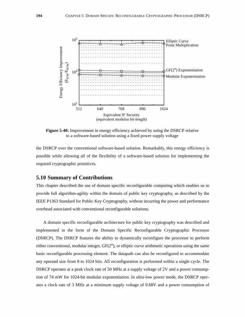
194 CHAPTER 5 DOMAIN SPECIFIC RECONFIGURABLE CRYPTOGRAPHIC PROCESSOR (DSRCP)
the DSRCP over the conventional software-based solution. Remarkably, this energy efficiency is
possible while allowing all of the flexibility of a software-based solution for implementing the
required cryptographic primitives.
5.10 Summary of ContributionsThis chapter described the use of domain specific reconfigurable computing which enables us to
provide full algorithm-agility within the domain of public key cryptography, as described by the
IEEE P1363 Standard for Public Key Cryptography, without incurring the power and performance
overhead associated with conventional reconfigurable solutions.
A domain specific reconfigurable architecture for public key cryptography was described and
implemented in the form of the Domain Specific Reconfigurable Cryptographic Processor
(DSRCP). The DSRCP features the ability to dynamically reconfigure the processor to perform
either conventional, modular integer, GF(2n), or elliptic curve arithmetic operations using the same
basic reconfigurable processing element. The datapath can also be reconfigured to accommodate
any operand size from 8 to 1024 bits. All reconfiguration is performed within a single cycle. The
DSRCP operates at a peak clock rate of 50 MHz at a supply voltage of 2V and a power consump-
tion of 74 mW for 1024-bit modular exponentiation. In ultra-low power mode, the DSRCP oper-
ates a clock rate of 3 MHz at a minimum supply voltage of 0.68V and a power consumption of
512 640 768 896 1024101
102
103
Figure 5-40: Improvement in energy efficiency achieved by using the DSRCP relativeto a software-based solution using a fixed power supply voltage
Ene
rgy
Eff
icie
ncy
Impr
ovem
ent
(ES
/W/E
H/W
)
Equivalent IF Security(equivalent modulus bit-length)
GF(2n) Exponentiation
Modular Exponentiation
Elliptic CurvePoint Multiplication

5.10 SUMMARY OF CONTRIBUTIONS 195
525µW.
The DSRCP validates the thesis of Domain Specific Reconfigurability by demonstrating that
for the chosen domain of public key cryptography, a hardware-based solution with limited recon-
figurability can deliver the algorithm-agility of a software-based solution and the energy efficiency
of a hardware-based solution, without the high overhead costs associated with generic programma-
ble logic implementations. The resulting implementation achieves approximately two to three
orders of magnitude better energy efficiency than comparable software and FPGA-based imple-
mentations, while achieving performance levels that are comparable to previously reported hard-
ware-based implementations.

196 CHAPTER 5 DOMAIN SPECIFIC RECONFIGURABLE CRYPTOGRAPHIC PROCESSOR (DSRCP)
197197197
Chapter 6
ConclusionsThe popularity of wireless networks and the accompanying demand for portable computing sys-
tems requires the development of energy-efficient hardware that is capable of providing a wide
range of functionality in an energy-constrained environment that exhibits time-varying quality
requirements. As a result, adaptive energy-scalable approaches are required in order to minimize
the energy consumption by allowing the system to adapt to the current operating (i.e., quality)
requirements. This energy-scalable approach enables the energy consumption of the system to be
based on the average-case as opposed to the worst-case, leading to substantial improvements in the
system’s operational lifetime. In addition, the lack of a coherent wireless security architecture has
resulted in many different types of cryptographic primitives being used, requiring some form of
algorithm agility in order to maximize the portable systems’ utility. Conventional solutions such as
software provide the required flexibility but are too energy-intensive, whereas dedicated hardware
is energy-efficient but not algorithm agile. A possible compromise exists in the form of domain
specific processing which utilizes limited reconfigurability to provide a range of functionality that
allows an entire domain, in this case asymmetric cryptography, to be implemented in a very effi-
cient manner. By limiting the degree of reconfigurability, the overhead associated with conven-
tional programmable logic (e.g., FPGA’s) is minimized, while still providing the required degree
of algorithm agility. The work described in this dissertation has demonstrated the value of using
both energy-scalable approaches and domain specific processing through two proof of concept
implementations: the Energy Scalable Encryption Processor (ESEP) and the Domain Specific
Reconfigurable Cryptographic Processor (DSRCP).

198 CHAPTER 6 CONCLUSIONS
6.1 Summary of ContributionsThe work described in this dissertation began with the development of an optimized software-
based solution for implementing the required arithmetic functions required by the various public
key algorithms. The resulting implementation was used to characterize the energy efficiency of a
software-based implementation running on the StrongARM SA-1100 low power processor. The
resulting analysis showed that the required primitives consume several mJ of energy per operation;
the equivalent of encrypting 10’s of Mbytes of data using secret key cryptographic algorithms. In
addition, certain operations such as GF(2n) multiplication and exponentiation were found to be
over an order of magnitude less efficient than equivalent integer-based operations running on a
general purpose processor such as the SA-1100. A small modification to the processor’s multipli-
cation unit was proposed which simulation indicated would eliminate this inefficiency with only a
small amount of overhead (<10%) in terms of both performance and area.
The thesis of Energy Scalability was then addressed, motivated by the time-varying quality
and throughput requirements that are inherent in wireless networks, and the overriding desire to
maximize the operational lifetime of the portable computing systems’ used in wireless applica-
tions. Energy scalable computing is most useful where data rates and quality requirements vary
greatly over time. In terms of cryptographic applications this occurs in the data encryption func-
tion which ties secret key ciphers to the wireless data stream. As a result, we proposed the develop-
ment of an energy scalable architecture for providing data encryption. The resulting architecture,
and Energy Scalability thesis, were then verified using a proof-of-concept implementation: the
Energy Scalable Encryption Processor (ESEP). The ESEP utilized a scalable architecture and
novel high-efficiency embedded power converter in order to dynamically adjust both the level of
security that was being provided, and the processor’s supply voltage. Experimental data verified
the thesis of Energy Scalability by demonstrating that the system’s energy consumption can be
reduced by a factor of 7 as a function of throughput, and a factor of 30 as a function of the security
level being provided. Using this energy-scalable implementation, the energy consumption required
to encrypt an example compressed video stream was reduced by a factor of 4. In addition, the
ESEP was found to be over two orders of magnitude more energy efficient than an optimized soft-
ware-based solution.
The embedded power converter used in within the ESEP demonstrated the benefits of utilizing
a hybrid delay-line and PLL-based fixed-frequency PWM architecture for doing low load power
conversion. The hybrid approach used enabled high efficiencies (80-96%) across a wide variety of
6.2 FUTURE WORK 199
loads ranging from 10-100’s mW, and the converter’s control architecture has also demonstrated
the ability to achieve high efficiencies at loads down to 10’s of µW, enabling variable voltage sup-
ply techniques to be used in a variety of portable applications. Variable supply techniques require
us to rethink the conventional view of the power supply in energy-constrained system design as the
supply is no longer a fixed value. Instead, the power supply becomes another system parameter
that can be optimized to satisfy a given set of design constraints, such as performance or energy
consumption, which can change with time. Exposing the power supply in this manner yields a very
powerful tool for developing energy-constrained systems in a variety of applications.
The thesis of Domain Specific Reconfigurability was illustrated using the domain of public
key cryptography as defined by the IEEE P1363 standard. Analysis of the standard yielded an
instruction set that required a variety of arithmetic functions over modular integer fields, binary
Galois Fields, and Elliptic Curves built upon binary Galois Fields. The resulting ISA was then
implemented in the Domain Specific Reconfigurable Cryptographic Processor (DSRCP), which
represented the first reported hardware-based solution capable of implementing such a wide vari-
ety of cryptographic primitives. The DSRCP utilized a datapath that can be dynamically reconfig-
ured in a single cycle to accommodate any operand size from 8 to 1024 bits. The architecture was
fully programmable in the sense that it can accommodate any odd integer modulus, characteristic
polynomial for GF(2n) ( ), or valid Elliptic Curve. The DSRCP validated the thesis of
Domain Specific Reconfigurability by demonstrating that for the chosen domain of public key
cryptography, a hardware-based solution with limited reconfigurability can deliver the algorithm-
agility of a software-based solution and the energy efficiency of a hardware-based solution, with-
out the high overhead costs associated with generic programmable logic implementations. Experi-
mental results indicated that the DSRCP achieves approximately two to three orders of magnitude
better energy efficiency than comparable software- and FPGA-based implementations, while
achieving, and in some instances surpassing, the performance and energy-efficiency of hardware-
based solutions.
6.2 Future WorkThe work described in this dissertation represents only the beginning in terms of issues that need
to be addressed in regards to developing energy scalable solutions and techniques. A great deal of
work remains to be done at all levels of the system design hierarchy in terms of both the hardware
and software. In addition, at a higher level the whole theory of energy scalability needs to be prop-
erly formalized, and a common framework and set of metrics developed in order to properly define
8 n 1024≤ ≤
200 CHAPTER 6 CONCLUSIONS
and characterize the notion of energy scalable computing. This will ultimately enable system
designers to develop formal design methods and evaluation criteria for future energy scalable sys-
tems.
The work described in Section 3.7.2 introduced the notion of energy scalable software as a
means of reducing the energy consumption of conventional software-based solutions during peri-
ods of inactivity on the processor. There remains a great deal of work to be done in regards to aug-
menting these basic results to incorporate energy-scalable algorithmic techniques, such as those
proposed for video compression software. Unfortunately, it is not readily apparent that the same
techniques such as trading off computational accuracy can be applied to cryptographic algorithms.
Cryptographic algorithms by design produce uncorrelated results when the inputs differ in even
the smallest detail (e.g., a single bit change in the input produces seemingly random output). One
alternative in secret key algorithms, which utilize an iterative round-based approach, is to limit the
number of iterations performed. However, work remains to be done in regards to characterizing
how security varies as a function of the number of iterations. Future secret key algorithm designs
could use the variable-iteration approach as a design criteria in the hope of developing an energy-
scalable encryption algorithm. Public key algorithms appear to have no such equivalent inherent
scalability. Instead, public key algorithms appear to require the use of multiple instantiations of the
algorithm with different key sizes and values, though future research might yield energy-scalable
public key algorithms as well.
The development of the DSRCP illustrated how domain specific processing can be used in
public key cryptographic applications. A natural extension of this work is the development of a
secret key analogue of the DSRCP based upon the ongoing Advanced Encryption Standard speci-
fication. The domain of secret key cryptography presents considerably different design challenges
due to the ability to tailor algorithm designs to conventional general purpose processing architec-
tures. The resulting architecture would likely differ considerably from that of the DSRCP, utilizing
a systolic array-based approach, with each processing element providing a reduced set of conven-
tional arithmetic instructions. Future research will enable the evaluation of this approach, as well
as help to determine the optimal implementation parameters in terms of the array size and instruc-
tion set. Ultimately a proof-of-concept implementation could be developed similar to the DSRCP
to allow experimental results to be gathered and conclusions drawn.

201
Recently very powerful implementation-based attacks such as power analysis and fault injec-
tion have been proposed as a means of attacking hardware-based cryptographic applications.
These attacks have yielded extremely good results, breaking many existing systems (such as the
smartcard-based systems commonly used in portable applications) in a matter of minutes once the
initial characterization has been performed. Hence, research needs to be done to develop imple-
mentation techniques to counteract these attacks. Unfortunately, the problem is made considerably
more difficult due to the constraints placed upon the designer by the portable nature of the applica-
tions. As an example, consider the case of power analysis. A straight-forward solution is to utilize
some form of constant-bias, current-steering logic in order to eliminate any tell-tale signatures in
the processor’s power consumption, at the cost of a large degree of static power consumption. In
conventional desktop situations the additional power consumption isn’t a concern and the solution
is acceptable, whereas in an energy-constrained portable application this approach is infeasible.
Future research will enable security system designers to develop both algorithmic and implemen-
tation-specific techniques to address these new attacks in constrained environments
Currently one of the main consumer concerns for the widespread acceptance of wireless net-
works is security. In the past system developers have all but ignored security in commercial wire-
less applications - the wide spread fraud that plagues the cellular phone industry today is a
damning testimonial of this fact. In the future, portable chipset developers will need to consider the
needs of security applications and develop extensions to their processors that facilitate security in
the same manner that DSP’s today feature video and channel/error coding extensions in their
ISA’s. However, work remains to be done to determine what these extensions will be, and how
they will best be integrated into existing architectures. The aforementioned multiplier unit modifi-
cation represents an initial step in this direction.
The work described in this dissertation focuses primarily on low-level algorithmic hardware-
based solutions for cryptographic applications in portable environments. Additional research is
required at a higher level in terms of developing energy-efficient security protocols for wireless
systems. In particular, the question remains to be answered if there are ways to exploit the distribu-
tion of computation and energy resources in the network, such that the most constrained nodes do
the least amount of work. While similar work has been done in regards to video compression
[104], the need for trust and authentication make the problem considerably more difficult in the
case of security.

202
In the past the focus in integrated circuit design has been the Application Specific Integrated
Circuit (ASIC) which typically operated from a fixed power supply to perform a given function in
a very efficient manner. However, the ever increasing demand for functionality and portability has
ushered in the era of the energy-scalable Domain Specific Integrated Circuit (DSIC) (no, we don’t
know what happened to BSIC and CSIC...). DSIC’s provide a much greater array of functionality
than their ASIC counterparts at the cost of only a small amount of overhead in terms of perfor-
mance/area, while yielding significantly better energy-efficiency due to their energy-scalable char-
acteristics. The design methodology utilized in this dissertation represents an example of how to
develop a DSIC and extend it using energy-scalable features such as embedded variable-output
power converters. The resulting research illustrates both the feasibility of this approach and the
advantages over conventional software, hardware, and programmable logic-based solutions.
203
References
[1] M. Abe and H. Morita, “Higher radix nonrestoring modular multiplication algorithm andpublic-key LSI architecture with limited hardware resources,” Advances in Cryptology -ASIACRYPT’94, Springer-Verlag, 1995, pp. 365-375.
[2] L.M. Adleman, “A subexponential algorithm for the discrete logarithm problem with appli-cations to cryptography,” Proceedings of the IEEE 20th Annual Symposium on Foundationsof Computer Science, 1979, pp. 55-60.
[3] L.M. Adleman and J. DeMarrais, “A subexponential algorithm for discrete logarithms overall finite fields,” Advances in Cryptography - CRYPTO’93, Springer-Verlag 1993, pp. 147-158.
[4] Advanced RISC Machines Ltd., ARM Software Development Toolkit v2.11: User guide,May 1997.
[5] G.B. Agnew, R.C. Mullin, I.M. Onyszchuk, and S.A. Vanstone, “An implementation for afast public-key cryptosystem,” Journal of Cryptology, vol. 3, no. 2, pp. 63-79, 1991.
[6] G.B. Agnew, R.C. Mullin, S. A. Vanstone, “An Implementation of Elliptic Curve Crypto-systems over GF(2155),” IEEE J. of Selected Areas in Communications, vol. 11, no. 5, pp.804-813, June 1993.
[7] R. Anderson, E. Biham, and L. Knudsen, “Serpent: a proposal for the Advanced EncryptionStandard,” First Advanced Encryption Standard (AES) Conference, 1998.
[8] R. Anderson and M. Kuhn, “Tamper resistance -- a cautionary note,” in Proc. SecondUSENIX Workshop on Electronic Commerce, 1996.
[9] Altera Corporation, APEX 20K Programmable Logic Device Family Data Sheet v2.06,March 2000.
[10] S. Arno and F.S. Wheeler, “Signed digit representations of minimal Hamming weight,”IEEE Transactions on Computers, vol. 42, no. 8, August 1993, pp. 1007-1010.
[11] E. Bach and J. Shallit, Algorithmic Number Theory, Volume 1: Efficient Algorithms, MITPress, 1996.
[12] D.V. Bailey and C. Paar, “Optimal extension fields for fast arithmetic in public-key algo-rithms,” in Advances in Cryptology - Proceedings of CRYPTO’98, Springer-Verlag 1998, pp.472-485.
[13] T. Barber, P.Carvey, and A. P. Chandrakasan, “Designing for wireless LAN communica-tions,” IEEE Circuits Devices Magazine, vol. 12, no. 4, pp. 29-33, 1996.
204
[14] L.E. Bassham, “Efficiency testing of ANSI C implementations of round 1 candidate algo-rithms for the Advanced Encryption Standard,” Third Advanced Encryption Standard (AES)Conference, 2000, pp. 136-148.
[15] D. Beauregard, Efficient Algorithms for Implementing Elliptic Curve Public-Key Schemes,Master’s Thesis, Worcester Polytechnic Institute, May 1996.
[16] E.R. Berlekamp, “Bit-serial Reed-Solomon encoders,” IEEE Transactions on InformationTheory, vol. IT-28, 1982, pp. 869-874.
[17] T. Beth and D. Gollmann, “Algorithm engineering for public key algorithms,” IEEE Journalon Selected Areas in Communications, vol. 7, no. 4, May 1989, pp. 458-465.
[18] I. Blake, G. Seroussi, and N. Smart, Elliptic Curves in Cryptography, Cambridge UniversityPress, 1999.
[19] L. Blum, M. Blum, and M. Shub, “A simple unpredictable pseudorandom number genera-tor,” SIAM Journal on Computing, vol. 15, no. 2, pp. 364-383, May 1986.
[20] T. Blum and C. Paar, “Montgomery modular exponentiation on reconfigurable hardware,”14th IEEE Symposium on Computer Arithmetic (ARITH-14), 1999.
[21] E.F. Brickell, “A fast modular multiplication algorithm with application in public key cryp-tography,” Advances in Cryptology -- CRYPTO’82, Plenum Press, 1983, pp. 51-60.
[22] C. Burwick, D. Coppersmith, E. D’Avignon, R. Gennaro, S. Halevi, C. Jutla, S.M. Matyas,L. O’Connor, M. Peyravian, D. Safford, and N. Zunic, “Mars - a candidate cipher for AES,”First Advanced Encryption Standard (AES) Conference, 1998.
[23] Certicom, http://www.certicom.com
[24] A. P. Chandrakasan, S. Sheng, and R. W. Brodersen, “Low-power CMOS digital design,”IEEE Journal of Solid-State Circuits, vol. 27, pp. 473-484, April 1992.
[25] A.P. Chandrakasan and R.W. Brodersen, Low Power Digital CMOS Design, Kluwer Aca-demic Publishers, May 1995.
[26] CERT Coordination Center, Advisory CA-99-16 Buffer Overflow in Sun Solstice AdminSuite Daemon sadmind, December 14, 1999.
[27] D. Chaum, “Blind signatures for untraceable payments,” Advances in Cryptology - Proceed-ings of CRYPTO’82, Plenum Press, 1983, pp. 199-203.
[28] P.-S. Chen, S.-A. Hwang, and C.-W. Wu, “A systolic RSA public key cryptosystem,” Pro-ceedings of the IEEE International Symposium on Circuits and Systems (ISCAS’96), 1996,pp. 408-411.
[29] P.G. Comba, “Exponentiation systems on the IBM PC,” IBM Systems Journal, vol. 29, no.4, 1990, pp. 526-538.
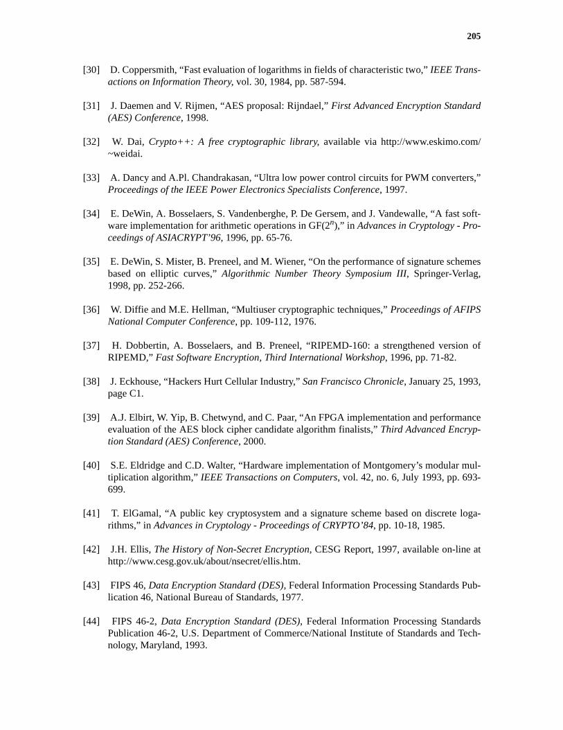
205
[30] D. Coppersmith, “Fast evaluation of logarithms in fields of characteristic two,” IEEE Trans-actions on Information Theory, vol. 30, 1984, pp. 587-594.
[31] J. Daemen and V. Rijmen, “AES proposal: Rijndael,” First Advanced Encryption Standard(AES) Conference, 1998.
[32] W. Dai, Crypto++: A free cryptographic library, available via http://www.eskimo.com/~weidai.
[33] A. Dancy and A.Pl. Chandrakasan, “Ultra low power control circuits for PWM converters,”Proceedings of the IEEE Power Electronics Specialists Conference, 1997.
[34] E. DeWin, A. Bosselaers, S. Vandenberghe, P. De Gersem, and J. Vandewalle, “A fast soft-ware implementation for arithmetic operations in GF(2n),” in Advances in Cryptology - Pro-ceedings of ASIACRYPT’96, 1996, pp. 65-76.
[35] E. DeWin, S. Mister, B. Preneel, and M. Wiener, “On the performance of signature schemesbased on elliptic curves,” Algorithmic Number Theory Symposium III, Springer-Verlag,1998, pp. 252-266.
[36] W. Diffie and M.E. Hellman, “Multiuser cryptographic techniques,” Proceedings of AFIPSNational Computer Conference, pp. 109-112, 1976.
[37] H. Dobbertin, A. Bosselaers, and B. Preneel, “RIPEMD-160: a strengthened version ofRIPEMD,” Fast Software Encryption, Third International Workshop, 1996, pp. 71-82.
[38] J. Eckhouse, “Hackers Hurt Cellular Industry,” San Francisco Chronicle, January 25, 1993,page C1.
[39] A.J. Elbirt, W. Yip, B. Chetwynd, and C. Paar, “An FPGA implementation and performanceevaluation of the AES block cipher candidate algorithm finalists,” Third Advanced Encryp-tion Standard (AES) Conference, 2000.
[40] S.E. Eldridge and C.D. Walter, “Hardware implementation of Montgomery’s modular mul-tiplication algorithm,” IEEE Transactions on Computers, vol. 42, no. 6, July 1993, pp. 693-699.
[41] T. ElGamal, “A public key cryptosystem and a signature scheme based on discrete loga-rithms,” in Advances in Cryptology - Proceedings of CRYPTO’84, pp. 10-18, 1985.
[42] J.H. Ellis, The History of Non-Secret Encryption, CESG Report, 1997, available on-line athttp://www.cesg.gov.uk/about/nsecret/ellis.htm.
[43] FIPS 46, Data Encryption Standard (DES), Federal Information Processing Standards Pub-lication 46, National Bureau of Standards, 1977.
[44] FIPS 46-2, Data Encryption Standard (DES), Federal Information Processing StandardsPublication 46-2, U.S. Department of Commerce/National Institute of Standards and Tech-nology, Maryland, 1993.
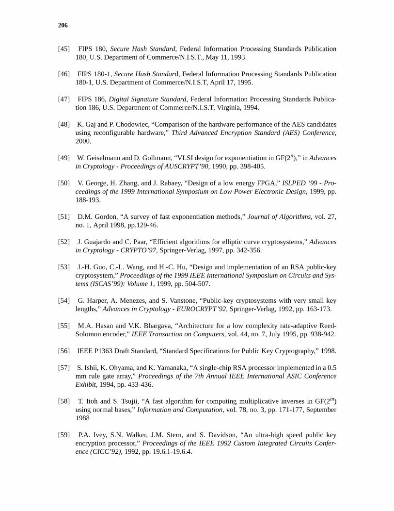
206
[45] FIPS 180, Secure Hash Standard, Federal Information Processing Standards Publication180, U.S. Department of Commerce/N.I.S.T., May 11, 1993.
[46] FIPS 180-1, Secure Hash Standard, Federal Information Processing Standards Publication180-1, U.S. Department of Commerce/N.I.S.T, April 17, 1995.
[47] FIPS 186, Digital Signature Standard, Federal Information Processing Standards Publica-tion 186, U.S. Department of Commerce/N.I.S.T, Virginia, 1994.
[48] K. Gaj and P. Chodowiec, “Comparison of the hardware performance of the AES candidatesusing reconfigurable hardware,” Third Advanced Encryption Standard (AES) Conference,2000.
[49] W. Geiselmann and D. Gollmann, “VLSI design for exponentiation in GF(2n),” in Advancesin Cryptology - Proceedings of AUSCRYPT’90, 1990, pp. 398-405.
[50] V. George, H. Zhang, and J. Rabaey, “Design of a low energy FPGA,” ISLPED ‘99 - Pro-ceedings of the 1999 International Symposium on Low Power Electronic Design, 1999, pp.188-193.
[51] D.M. Gordon, “A survey of fast exponentiation methods,” Journal of Algorithms, vol. 27,no. 1, April 1998, pp.129-46.
[52] J. Guajardo and C. Paar, “Efficient algorithms for elliptic curve cryptosystems,” Advancesin Cryptology - CRYPTO’97, Springer-Verlag, 1997, pp. 342-356.
[53] J.-H. Guo, C.-L. Wang, and H.-C. Hu, “Design and implementation of an RSA public-keycryptosystem,” Proceedings of the 1999 IEEE International Symposium on Circuits and Sys-tems (ISCAS’99): Volume 1, 1999, pp. 504-507.
[54] G. Harper, A. Menezes, and S. Vanstone, “Public-key cryptosystems with very small keylengths,” Advances in Cryptology - EUROCRYPT’92, Springer-Verlag, 1992, pp. 163-173.
[55] M.A. Hasan and V.K. Bhargava, “Architecture for a low complexity rate-adaptive Reed-Solomon encoder,” IEEE Transaction on Computers, vol. 44, no. 7, July 1995, pp. 938-942.
[56] IEEE P1363 Draft Standard, “Standard Specifications for Public Key Cryptography,” 1998.
[57] S. Ishii, K. Ohyama, and K. Yamanaka, “A single-chip RSA processor implemented in a 0.5mm rule gate array,” Proceedings of the 7th Annual IEEE International ASIC ConferenceExhibit, 1994, pp. 433-436.
[58] T. Itoh and S. Tsujii, “A fast algorithm for computing multiplicative inverses in GF(2m)using normal bases,” Information and Computation, vol. 78, no. 3, pp. 171-177, September1988
[59] P.A. Ivey, S.N. Walker, J.M. Stern, and S. Davidson, “An ultra-high speed public keyencryption processor,” Proceedings of the IEEE 1992 Custom Integrated Circuits Confer-ence (CICC’92), 1992, pp. 19.6.1-19.6.4.
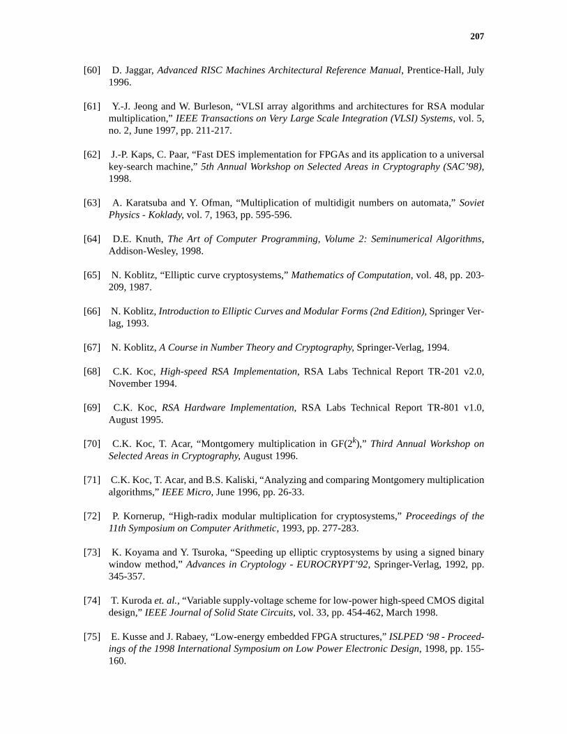
207
[60] D. Jaggar, Advanced RISC Machines Architectural Reference Manual, Prentice-Hall, July1996.
[61] Y.-J. Jeong and W. Burleson, “VLSI array algorithms and architectures for RSA modularmultiplication,” IEEE Transactions on Very Large Scale Integration (VLSI) Systems, vol. 5,no. 2, June 1997, pp. 211-217.
[62] J.-P. Kaps, C. Paar, “Fast DES implementation for FPGAs and its application to a universalkey-search machine,” 5th Annual Workshop on Selected Areas in Cryptography (SAC’98),1998.
[63] A. Karatsuba and Y. Ofman, “Multiplication of multidigit numbers on automata,” SovietPhysics - Koklady, vol. 7, 1963, pp. 595-596.
[64] D.E. Knuth, The Art of Computer Programming, Volume 2: Seminumerical Algorithms,Addison-Wesley, 1998.
[65] N. Koblitz, “Elliptic curve cryptosystems,” Mathematics of Computation, vol. 48, pp. 203-209, 1987.
[66] N. Koblitz, Introduction to Elliptic Curves and Modular Forms (2nd Edition), Springer Ver-lag, 1993.
[67] N. Koblitz, A Course in Number Theory and Cryptography, Springer-Verlag, 1994.
[68] C.K. Koc, High-speed RSA Implementation, RSA Labs Technical Report TR-201 v2.0,November 1994.
[69] C.K. Koc, RSA Hardware Implementation, RSA Labs Technical Report TR-801 v1.0,August 1995.
[70] C.K. Koc, T. Acar, “Montgomery multiplication in GF(2k),” Third Annual Workshop onSelected Areas in Cryptography, August 1996.
[71] C.K. Koc, T. Acar, and B.S. Kaliski, “Analyzing and comparing Montgomery multiplicationalgorithms,” IEEE Micro, June 1996, pp. 26-33.
[72] P. Kornerup, “High-radix modular multiplication for cryptosystems,” Proceedings of the11th Symposium on Computer Arithmetic, 1993, pp. 277-283.
[73] K. Koyama and Y. Tsuroka, “Speeding up elliptic cryptosystems by using a signed binarywindow method,” Advances in Cryptology - EUROCRYPT’92, Springer-Verlag, 1992, pp.345-357.
[74] T. Kuroda et. al., “Variable supply-voltage scheme for low-power high-speed CMOS digitaldesign,” IEEE Journal of Solid State Circuits, vol. 33, pp. 454-462, March 1998.
[75] E. Kusse and J. Rabaey, “Low-energy embedded FPGA structures,” ISLPED ‘98 - Proceed-ings of the 1998 International Symposium on Low Power Electronic Design, 1998, pp. 155-160.
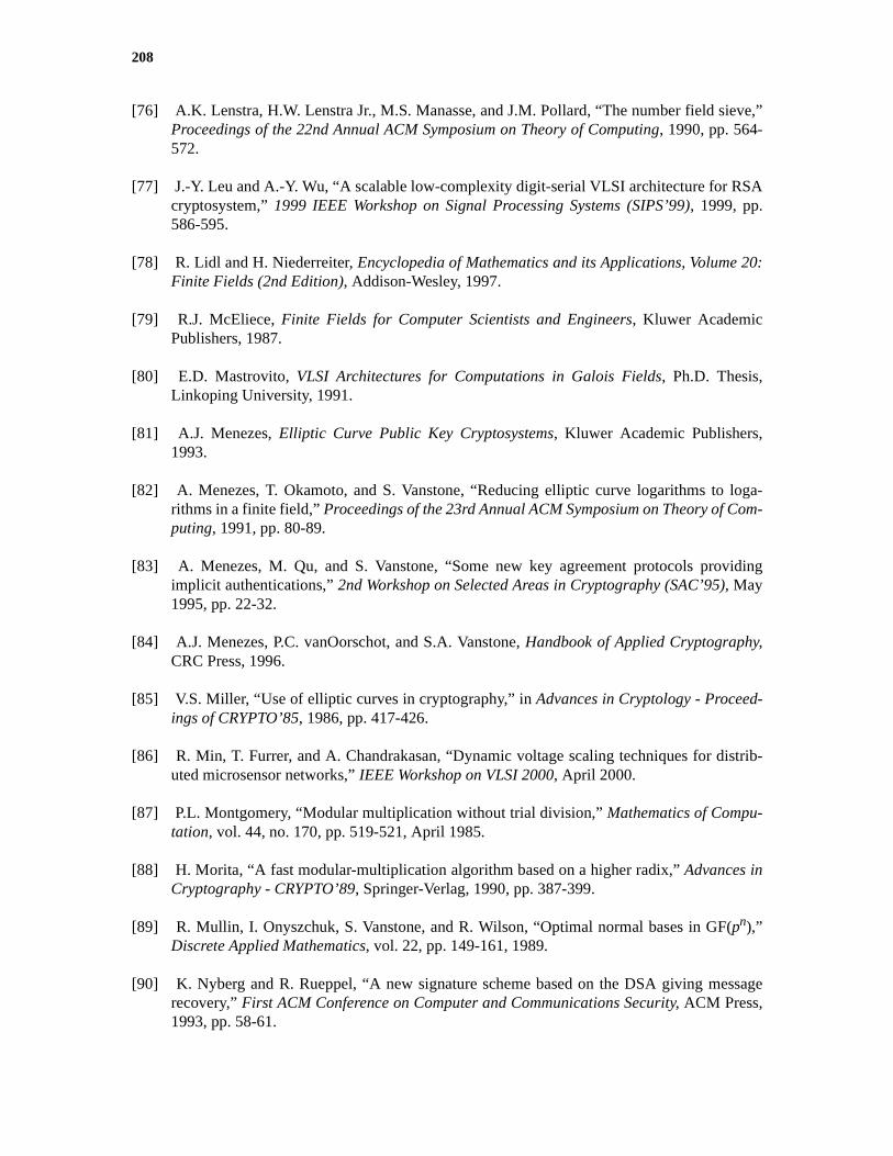
208
[76] A.K. Lenstra, H.W. Lenstra Jr., M.S. Manasse, and J.M. Pollard, “The number field sieve,”Proceedings of the 22nd Annual ACM Symposium on Theory of Computing, 1990, pp. 564-572.
[77] J.-Y. Leu and A.-Y. Wu, “A scalable low-complexity digit-serial VLSI architecture for RSAcryptosystem,” 1999 IEEE Workshop on Signal Processing Systems (SIPS’99), 1999, pp.586-595.
[78] R. Lidl and H. Niederreiter, Encyclopedia of Mathematics and its Applications, Volume 20:Finite Fields (2nd Edition), Addison-Wesley, 1997.
[79] R.J. McEliece, Finite Fields for Computer Scientists and Engineers, Kluwer AcademicPublishers, 1987.
[80] E.D. Mastrovito, VLSI Architectures for Computations in Galois Fields, Ph.D. Thesis,Linkoping University, 1991.
[81] A.J. Menezes, Elliptic Curve Public Key Cryptosystems, Kluwer Academic Publishers,1993.
[82] A. Menezes, T. Okamoto, and S. Vanstone, “Reducing elliptic curve logarithms to loga-rithms in a finite field,” Proceedings of the 23rd Annual ACM Symposium on Theory of Com-puting, 1991, pp. 80-89.
[83] A. Menezes, M. Qu, and S. Vanstone, “Some new key agreement protocols providingimplicit authentications,” 2nd Workshop on Selected Areas in Cryptography (SAC’95), May1995, pp. 22-32.
[84] A.J. Menezes, P.C. vanOorschot, and S.A. Vanstone, Handbook of Applied Cryptography,CRC Press, 1996.
[85] V.S. Miller, “Use of elliptic curves in cryptography,” in Advances in Cryptology - Proceed-ings of CRYPTO’85, 1986, pp. 417-426.
[86] R. Min, T. Furrer, and A. Chandrakasan, “Dynamic voltage scaling techniques for distrib-uted microsensor networks,” IEEE Workshop on VLSI 2000, April 2000.
[87] P.L. Montgomery, “Modular multiplication without trial division,” Mathematics of Compu-tation, vol. 44, no. 170, pp. 519-521, April 1985.
[88] H. Morita, “A fast modular-multiplication algorithm based on a higher radix,” Advances inCryptography - CRYPTO’89, Springer-Verlag, 1990, pp. 387-399.
[89] R. Mullin, I. Onyszchuk, S. Vanstone, and R. Wilson, “Optimal normal bases in GF(pn),”Discrete Applied Mathematics, vol. 22, pp. 149-161, 1989.
[90] K. Nyberg and R. Rueppel, “A new signature scheme based on the DSA giving messagerecovery,” First ACM Conference on Computer and Communications Security, ACM Press,1993, pp. 58-61.
209
[91] J.K. Omura and J.L. Massey, Computational Method and Apparatus for Finite Field Arith-metic, U.S. Patent 4,587,627, 1986.
[92] P.C. van Oorschot and M.J. Wiener, “Parallel collision search with cryptanalytic applica-tions,” Journal of Cryptology, vol. 12, 1999, pp. 1-28.
[93] G. Orlando and C. Paar, “A super-serial Galois Fields multiplier for FPGAs and its applica-tion to public-key algorithms,” Seventh Annual IEEE Symposium on Field-ProgrammableCustom Computing Machines (FCCM’99), 1999.
[94] H. Orup, “Simplifying quotient determination in high-radix modular multiplication,” Pro-ceedings of the 12th Symposium on Computer Arithmetic, 1995, pp.193-199.
[95] H. Orup, E. Svendsen, and E. Andreasen, “VICTOR an efficient RSA hardware implemen-tation,” Advances in Cryptography - EUROCRYPT’90, Springer-Verlag, 1991, pp. 245-252.
[96] C. Paar and P. Soria-Rodriguez, “Fast Arithmetic Architectures for Public-Key Algorithmsover Galois Fields GF((2n)m),” Advances in Cryptology - Proceedings of EUROCRYPT’97,Springer Verlag 1997, pp. 363-378.
[97] J. M. Pollard, “The fast fourier transform in a finite field,” Mathematics of Computation,vol. 25, no. 114, April 1971, pp. 365-374.
[98] J.M. Pollard, “Monte Carlo methods for index computation mod p,” Mathematics of Com-putation, vol. 32, 1978, pp. 918-924.
[99] C. Pomerance, “The quadratic sieve factoring algorithm,” Advances in Cryptology - Pro-ceedings of EUROCRYPT’84, 1985, pp. 169-182.
[100] R.J. Proebsting, “Speed enhancement techniques for CMOS circuits,” U.S. Patent4,985,643.
[101] J.-J. Quisquater and C. Couvreur, “Fast decipherment algorithm for RSA public-key crypto-system,” Electronics Letters, vol. 18, no. 21, pp. 905-907, October 1982.
[102] J. Rabaey et. al., Pleaides Project Home Page, http://bwrc.eecs.berkeley.edu/Research/Configurable_Architectures
[103] M.O. Rabin, “Digitalized signatures and public-key functions as intractable as factoriza-tion,” Massachusetts Institute of Technology Laboratory for computer Science TechnicalReport 212 (MIT/LCS/TR-212), 1979.
[104] W.B. Rabiner and A.P. Chandrakasan, “Network-driven motion estimation for wirelessvideo terminals,” IEEE Transactions on Circuits and Systems for Video Technology, vol. 7,no. 4, August 1997, pp. 644-653.
[105] M. Riaz and H.M. Heys, “The FPGA implementation of the RC6 and CAST-256 encryptionalgorithms,” Proceedings of the 1999 IEEE Canadian Conference on Electrical and Com-puter Engineering Volume 1, 1999.

210
[106] R.L. Rivest, “The MD4 message digest algorithm,” Internet RFC 1320, April 1992.
[107] R.L. Rivest, A. Shamir, and L.M. Adleman, “A method for obtaining digital signatures andpublic-key cryptosystems,” Communications of the ACM, vol. 21, no. 2, pp. 120-126, Febru-ary 1979.
[108] R. Rivest, M. Robshaw, R. Sidney, and Y. Yin, “The RC6 block cipher,” First AdvancedEncryption Standard (AES) Conference, 1998.
[109] M. Rosner, Elliptic Curve Cryptosystems on Reconfigurable Hardware, Master’s Thesis,Worcester Polytechnic Institute, May 1998.
[110] A. Royo, J. Moran, J.C. Lopez, “Design and implementation of a coprocessor for cryptogra-phy applications,” Proceedings of the European Design and Test Conference (ED&TC’97),1997, pp. 213-217.
[111] RSA Security Inc., http://www.rsasecurity.com
[112] T. Sakuta, W. Lee, and P.T. Balsara, “Delay balanced multipliers for low power/low voltageDSRP core,” 1995 IEEE Symposium on Low Power Electronics, 1995, pp. 36-37.
[113] A. Satoh, Y. Kobayashi, H. Niijima, S. Munetoh, and S. Sone, “A high-speed small RSAencryption LSI with low power dissipation,” ISW’97 - Proceedings of First InternationalInformation Security Workshop, 1998.
[114] J. Sauerbrey, “A modular exponentiation unit based on systolic arrays,” Advances in Cryp-tography - AUSCRYPT’92, springer-Verlag, 1993, pp. 505-516.
[115] R. Schoof, “Counting points on elliptic curves over finite fields,” Journal Theorie des Nom-bres de Bordeaux, vol. 7, 1995, pp. 219-254.
[116] B. Schneier, Applied Cryptography Second Edition, John Wiley & Sons, 1996.
[117] B. Schneier, J. Kelsey, D. Whiting, D. Wagner, and C. Hall, “Twofish: a 128-bit blockcipher,” First Advanced Encryption Standard (AES) Conference, 1998.
[118] R. Schroeppel, H. Orman, S. O’Malley, and O. Spatscheck, “Fast key exchange with ellipticcurve systems,” in Advances in Cryptology - Proceedings of CRYPTO’95, 1995, pp. 43-56.
[119] H. Sedlak, “The RSA cryptography processor,” Advances in Cryptology - Proceedings ofEUROCRYPT’87, Springer-Verlag, 1987, pp. 127-142.
[120] G. Seroussi, Table of Low-Weight Binary Irreducible Polynomials, HP Labs TechnicalReport HPL-98-135, August 1998.
[121] M. Shand and J. Vuillemin, 'Fast implementations of RSA cryptography,” Proceedings ofthe 11th IEEE Symposium on Computer Arithmetic, 1993, pp. 252-259.
[122] T. Simon, A Low Power Video Compression Chip for Portable Applications, Ph.D. Thesis,Massachusetts Institute of Technology, 1999.
211
[123] S. Sutikno, A. Surya, and R. Effendi, “An implementation of El Gamal elliptic curves cryp-tosystems,” Proceedings of the 1998 IEEE Asia-Pacific Conference on Circuits and Systems(APCCAS’98), 1998, pp. 483-486.
[124] S. Sutikno, r. Effendi, and A. Surya, “Design and implementation of arithmetic processorGF(2155) for elliptic curve cryptosystems,” Proceedings of the 1998 IEEE Asia-Pacific Con-ference on Circuits and Systems (APCCAS’98), 1998, pp. 647-650.
[125] N. Takagi, “A radix-4 modular multiplication hardware algorithm for modular exponentia-tion,” IEEE Transactions on Computing, vol. 41, pp. 949-956, August 1992.
[126] N. Takagi and S. Yajima, “Modular multiplication hardware algorithms with a redundantrepresentation and their application to RSA cryptosystem,” IEEE Transaction on Comput-ers, vol. 41, July 1992, pp. 887-891.
[127] A. Tiountchik, “Systolic modular exponentiation via Montgomery algorithm,” ElectronicLetters, vol. 34, no. 9, April 1998, pp. 874-875.
[128] A. Vandemeulebroecke, “A single chip 1024 bits RSA processor,” Advances in Cryptology -EUROCRYPT’89, Springer-Verlag, 1990, pp. 219-236.
[129] U. V. Vazirani and V. V. Vazirani, “Efficient and secure pseudo-random number generation,”in Advances in Cryptology - Proceedings of CRYPTO’84, 1985, pp. 193-202.
[130] C.D. Walter, “Systolic modular multiplication,” IEEE Transactions on Computers, vol. 42,no. 3, March 1993, pp. 376-378.
[131] P.A. Wang, W.-C. Tsai, and C.B. Shung, “New VLSI architectures of RSA public-key cryp-tosystem,” Proceedings of the 1997 IEEE International Symposium on Circuits and Systems(ISCAS’97), pp. 2040-2043.
[132] G.-Y. Wei and M. Horowitz, “A low power switching power supply for self-clocked sys-tems,” Proceedings of the 1996 International Symposium on Low Power Electronics andDesign, 1996.
[133] N. Weste and K. Eshraghian, Principles of CMOS VLSI Design 2nd Edition, Addison-Wes-ley, 1993.
[134] H.C. Williams, “A modification of the RSA public-key encryption procedure,” IEEE Trans-actions on Information Theory, vol. 26, 1980, pp. 726-729.
[135] K. Wong, M. Wark, and E. Dawson, “A single-chip FPGA implementation of the dataencryption standard (DES) algorithm,” Proceedings of IEEE GLOBECOM’98 Volume 2,1998.
[136] Xilinx Inc., Virtex-E 1.8V Field Programmable Gate Array Data Sheet v1.3, May 2000.
[137] Xilinx Inc., A Simple Method of Estimating Power in XC4000XL/EX/E FPGAs, ApplicationBrief XBRF 014 v1.0, June 30, 1997.

212
[138] C.-C. Yang, T.-S. Chang, and C.-W. Jen, “A new RSA cryptosystem hardware design basedon Montgomery’s algorithm,” IEEE Transactions on Circuits and Systems - II: Analog andDigital Signal Processing, vol. 45, no. 7, July 1998, pp. 908-913.
[139] D. Yuliang, M. Zhigang, Y. Yizheng, W. Tao, “Implementation of RSA cryptoprocessorbased on Montgomery algorithm,” Proceedings of 5th International Conference Solid-Stateand Integrated Circuit Technology, 1998, pp. 524-526.
[140] K. Yiu and K. Peterson, “A single-chip VLSI implementation of the discrete exponentialpublic key distribution system,” IEEE Global Telecommunications Conference - GLOBE-COM’82, vol. 1, 1982, pp. 173-9.
[141] H. Zhang, V. Prabhu, V. George, M. Wan, M. Benes, A. Abnous, and J. Rabaey, “A 1V Het-erogeneous Reconfigurable Processor IC for Baseband Wireless Applications,” Proceedingsof the 2000 International Solid-State Circuits Conference, 2000, pp. 68-69.
[142] P.R. Zimmerman, The Official PGP User’s Guide, MIT Press, June 1995.
[143] D. Zurax, “On squaring and multiplying large integers,” Proceedings of the 11th Sympo-sium on Computer Arithmetic, 1993, pp. 260-271.
213213213
Appendix A
Energy Scalable Encryption Processor User’s ManualThis appendix serves as a general user’s manual for using the Energy Scalable Encryption Proces-
sor described in Chapter 4.
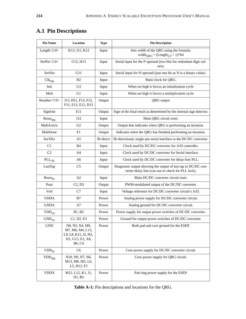
214 APPENDIX A ENERGY SCALABLE ENCRYPTION PROCESSOR USER’S MANUAL
A.1 Pin Descriptions
Pin Name Location Type Pin Description
Length<2:0> K13, J11, K12 Input Sets width of the QRG using the formula:widthQRG = (Length2:0 + 1)*64
SerPin<1:0> G12, H13 Input Serial input for the P operand (two bits for redundant digit val-ues).
SerNin G11 Input Serial input for N operand (just one bit as N is a binary value).
Clkqrg H2 Input Main clock for QRG.
Init G3 Input When set high it forces an initialization cycle
Mult G1 Input When set high it forces a multiplication cycle
Residue<7:0> J13, H11, F13, F12, F11, E13, E12, D13
Output QRG output
SignOut E11 Output Sign of the final result as determined by the internal sign detector.
Resetqrg J12 Input Main QRG circuit reset.
MultActive G2 Output Output that indicates when QRG is performing an iteration.
MultDone F1 Output Indicates when the QRG has finished performing an iteration.
SerXfer A5 Bi-direct Bi-directional, single-pin serial interface to the DC/DC converter.
C1 B4 Input Clock used by DC/DC converter for A/D controller.
C2 A4 Input Clock used by DC/DC converter for Serial interface.
PLLclk A6 Input Clock used by DC/DC converter for delay-line PLL.
LastTap C5 Output Diagnostic output showing the output of last tap in DC/DC con-verter delay line (can use to check for PLL lock).
Resetdc A2 Input Main DC/DC converter circuit reset.
Pout C2, D3 Output PWM-modulated output of the DC/DC converter.
Vref C7 Input Voltage reference for DC/DC converter circuit’s A/D.
VDDA B7 Power Analog power supply for DC/DC converter circuit.
GNDA A7 Power Analog ground for DC/DC converter circuit.
VDDsw B1, B2 Power Power supply for output power switches of DC/DC converter.
GNDsw C1, D2, E3 Power Ground for output power switches of DC/DC converter.
GND N8, N5, N4, M9, M7, M6, M4, L13,
L9, L8, K11, J2, H3, H1, G13, E2, A8,
B6, C4
Power Both pad and core ground for the ESEP.
VDDdc C6 Power Core power supply for DC/DC converter circuit.
VDDqrg N10, N9, N7, N6, M13, M8, M5, L6,
L5, H12, F2
Power Core power supply for QRG circuit.
VDDX M12, L12, K1, J1, D1, B5
Power Pad ring power supply for the ESEP.
Table A-1: Pin descriptions and locations for the QRG.
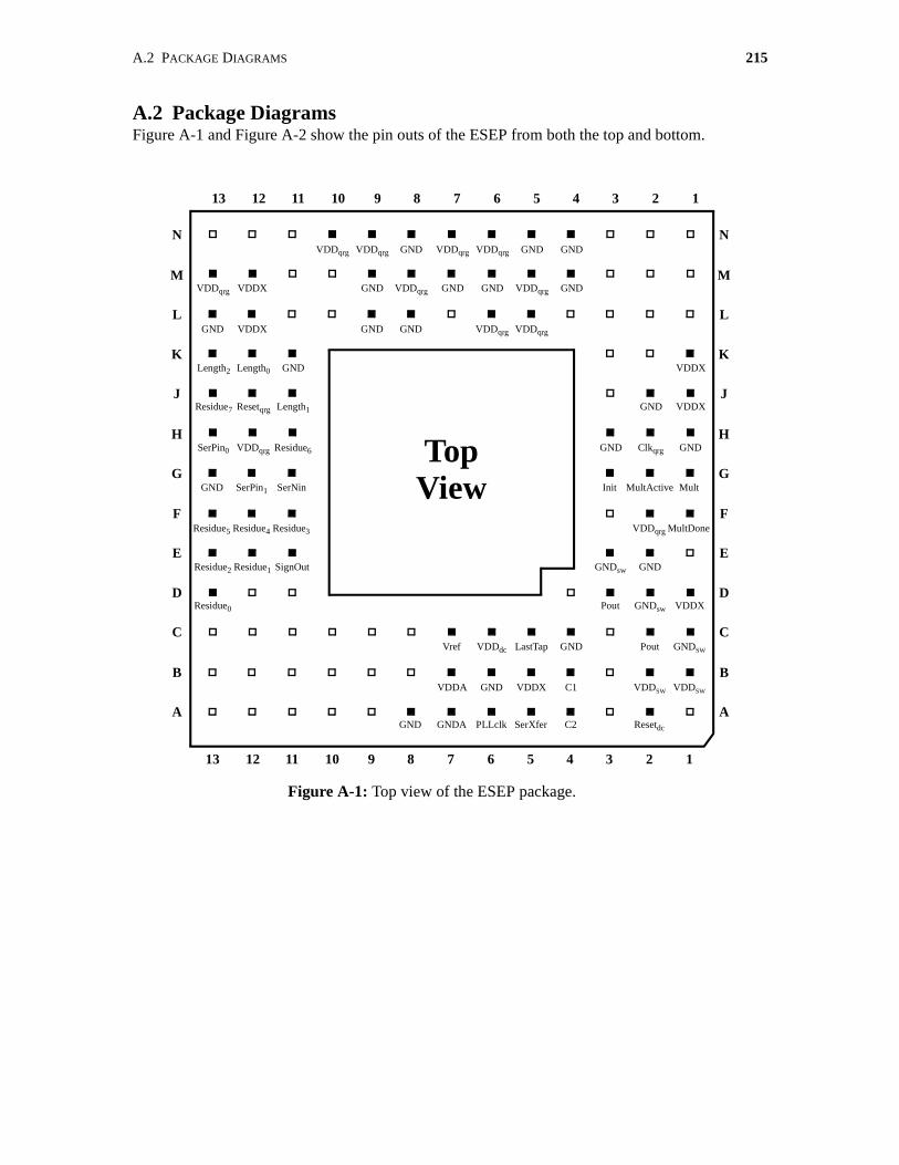
A.2 PACKAGE DIAGRAMS 215
A.2 Package DiagramsFigure A-1 and Figure A-2 show the pin outs of the ESEP from both the top and bottom.
GNDVDDqrg VDDqrg
VDDqrgGNDVDDqrg
GNDGNDVDDXGND
Length0 GNDLength2
Resetqrg Length1Residue7
VDDqrg Residue6SerPin0
SerPin1 SerNinGND
Residue4 Residue3Residue5
Residue1 SignOutResidue2
Residue0
GND
234569 710 8111213 1
B
C
D
E
F
G
H
J
K
L
M
N
TopView
Figure A-1: Top view of the ESEP package.
A
VDDqrg VDDqrg GND GND
GND GND VDDqrg
VDDqrg VDDqrg
VDDX
GND VDDX
GND Clkqrg GND
Init MultActive Mult
VDDqrg MultDone
GNDsw GND
Pout GNDsw VDDX
Vref VDDdc LastTap GND Pout GNDSW
VDDA GND VDDX C1 VDDSW
GNDA PLLclk SerXfer C2 Resetdc
234569 710 8111213 1
B
C
D
E
F
G
H
J
K
L
M
N
A
VDDX
VDDSW
GND

216 APPENDIX A ENERGY SCALABLE ENCRYPTION PROCESSOR USER’S MANUAL
A.3 Determining Clock Rate and Supply VoltageThis section describes methods for determining the required clock rate and supply voltage of the
QRG chip.
The scalable nature of the QRG implies that it will require a variable number of clock cycles in
order to perform an operation. The number of cycles that are required can be computed using the
formula:
(A.1)
Table A-2 provides a sample set of clock rates for the QRG chip assuming a 1 Mbps data rate.
GND VDDqrgVDDqrg
VDDqrg GND VDDqrg
GND GND VDDX GND
Length0GND Length2
ResetqrgLength1 Residue7
VDDqrgResidue6 SerPin0
SerPin1SerNin GND
Residue4Residue3 Residue5
Residue1SignOut Residue2
Residue0
GND
2 3 4 5 6 97 108 11 12 131
B
C
D
E
F
G
H
J
K
L
M
N
BottomView
Figure A-2: Bottom view of the ESEP package.
A
VDDqrgVDDqrgGNDGND
GNDGNDVDDqrg
VDDqrgVDDqrg
VDDX
GNDVDDX
GNDClkqrgGND
InitMultActiveMult
VDDqrgMultDone
GNDswGND
PoutGNDswVDDX
VrefVDDdcLastTapGNDPoutGNDSW
VDDAGNDVDDXC1VDDSW
GNDAPLLclkSerXferC2Resetdc
2 3 4 5 6 97 108 11 12 131
B
C
D
E
F
G
H
J
K
L
M
N
A
VDDX
VDDSW
GND
fCLKdata rate( ) # cycles per operation( )×
# bits per operation( )-----------------------------------------------------------------------------------------
N2log 4+
N2loglog------------------------------ fDATA×= =
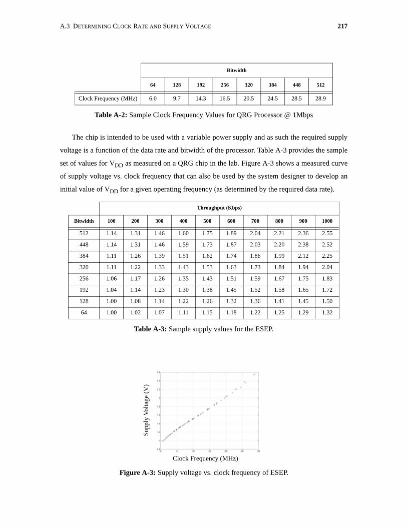
A.3 DETERMINING CLOCK RATE AND SUPPLY VOLTAGE 217
The chip is intended to be used with a variable power supply and as such the required supply
voltage is a function of the data rate and bitwidth of the processor. Table A-3 provides the sample
set of values for VDD as measured on a QRG chip in the lab. Figure A-3 shows a measured curve
of supply voltage vs. clock frequency that can also be used by the system designer to develop an
initial value of VDD for a given operating frequency (as determined by the required data rate).
Bitwidth
64 128 192 256 320 384 448 512
Clock Frequency (MHz) 6.0 9.7 14.3 16.5 20.5 24.5 28.5 28.9
Table A-2: Sample Clock Frequency Values for QRG Processor @ 1Mbps
Throughput (Kbps)
Bitwidth 100 200 300 400 500 600 700 800 900 1000
512 1.14 1.31 1.46 1.60 1.75 1.89 2.04 2.21 2.36 2.55
448 1.14 1.31 1.46 1.59 1.73 1.87 2.03 2.20 2.38 2.52
384 1.11 1.26 1.39 1.51 1.62 1.74 1.86 1.99 2.12 2.25
320 1.11 1.22 1.33 1.43 1.53 1.63 1.73 1.84 1.94 2.04
256 1.06 1.17 1.26 1.35 1.43 1.51 1.59 1.67 1.75 1.83
192 1.04 1.14 1.23 1.30 1.38 1.45 1.52 1.58 1.65 1.72
128 1.00 1.08 1.14 1.22 1.26 1.32 1.36 1.41 1.45 1.50
64 1.00 1.02 1.07 1.11 1.15 1.18 1.22 1.25 1.29 1.32
Table A-3: Sample supply values for the ESEP.
Figure A-3: Supply voltage vs. clock frequency of ESEP.
Clock Frequency (MHz)
Sup
ply
Vol
tage
(V
)
218 APPENDIX A ENERGY SCALABLE ENCRYPTION PROCESSOR USER’S MANUAL
A.4 Basic OperationThis section describes the basic operation of the QRG circuitry, which can perform two basic func-
tions: initialization and multiplication. Initialization is required to setup the modulus and seed
value that are to be used for the QRG. Both the modulus and seed are entered serially via SerNin
and SerPin<1:0> respectively. SerPin uses two pins in order to handle input digits from the
redundant number set {-1, 0, 1}. Note that for binary-valued inputs you can simply ground Ser-
Pin<1> and use SerPin<0> as a binary-valued serial port. Multiplication performs the QRG com-
putation:
(A.1)
where n = floor(log2log2N) is the number of bits that you are capable of extracting from each iter-
ation; it’s up to the system designer to ensure that only the n LSB of each result are used. A simple
way to determine n is to compute n = floor(log2(bitwidth of N)) (e.g., if N is a 512b value then n =
9 bits).
A.4.1 InitializationInitialization is performed to shift in the required operands and preload them into the required
internal registers (X & Y). The entire initialization function is performed via the Init, Ser-
Pin<1:0>, and SerNin inputs. Init is asserted and then after a 1 cycle delay (which enables the Ini-
tialization FSM to enable the appropriate internal circuitry) SerPin and SerNin inputs are applied
serially, starting with the MSB (or MSD in the case of SerPin). The number of values presented to
the SerPin and SerNin inputs depends on the current value of Length<2:0> input (which ulti-
mately defines the width of the QRG’s datapath). A sample timing diagram is shown in Figure A-
4. There’s no magic here... it’s just that simple! Note that all data is clocked on the rising edge of
Clk so data should be setup appropriately (sorry... I don’t have any setup/hold time information at
this time -- I suggest you use the negative edge of Clk to register the SerPin and SerNin data
inputs outside of the chip).
Note that once an “Init” cycle is started it must run to completion -- the QRG will ignore all
other requests until it has finished the process. Once the LSB of P and N have been loaded the user
must wait 3 cycles while the internal control logic resets itself before issuing another “Init” or
“Mult” request (i.e., you can assert Mult a minimum of (m + 4) cycles after asserting Init). The
resulting timing is shown in Figure A-4.
Residue n 1 0,–( ) LSBn P2 mod N( )=
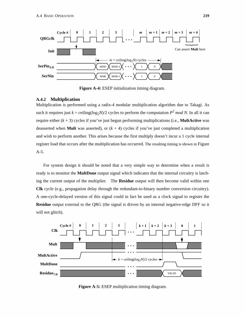
A.4 BASIC OPERATION 219
A.4.2 MultiplicationMultiplication is performed using a radix-4 modular multiplication algorithm due to Takagi. As
such it requires just k = ceiling(log2N)/2 cycles to perform the computation P2 mod N. In all it can
require either (k + 3) cycles if you’ve just begun performing multiplications (i.e., MultActive was
deasserted when Mult was asserted), or (k + 4) cycles if you’ve just completed a multiplication
and wish to perform another. This arises because the first multiply doesn’t incur a 1 cycle internal
register load that occurs after the multiplication has occurred. The resulting timing is shown in Figure
A-5.
For system design it should be noted that a very simple way to determine when a result is
ready is to monitor the MultDone output signal which indicates that the internal circuitry is latch-
ing the current output of the multiplier. The Residue output will then become valid within one
Clk cycle (e.g., propagation delay through the redundant-to-binary number conversion circuitry).
A one-cycle-delayed version of this signal could in fact be used as a clock signal to register the
Residue output external to the QRG (the signal is driven by an internal negative-edge DFF so it
will not glitch).
Figure A-4: ESEP initialization timing diagram.
QRGclk
Init
SerPin1:0
SerNin
MSD MSD-1
MSB MSB-1
1 0
1 0
. . .
. . .
. . .
m = ceiling(log2N) cycles
Cycle # 0 1 2 3 m m + 1 m + 2 m + 3 m + 4
{
Can assert Mult here
Figure A-5: ESEP multiplication timing diagram.
Clk
Mult
MultDone
Residue7:0
. . .
VALID
k = ceiling(log2N)/2 cycles
Cycle # 0 1 2 3 k + 1 k + 2 k + 3
MultActive
. . .
. . .
. . .
. . .
0 1
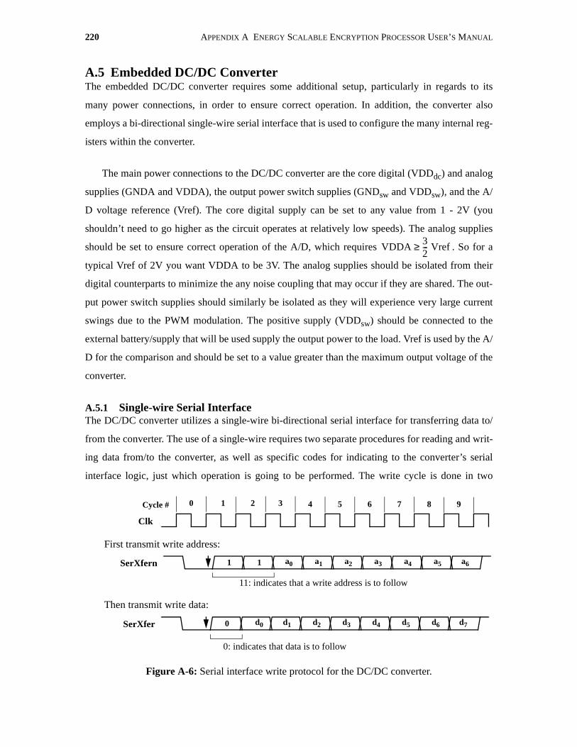
220 APPENDIX A ENERGY SCALABLE ENCRYPTION PROCESSOR USER’S MANUAL
A.5 Embedded DC/DC ConverterThe embedded DC/DC converter requires some additional setup, particularly in regards to its
many power connections, in order to ensure correct operation. In addition, the converter also
employs a bi-directional single-wire serial interface that is used to configure the many internal reg-
isters within the converter.
The main power connections to the DC/DC converter are the core digital (VDDdc) and analog
supplies (GNDA and VDDA), the output power switch supplies (GNDsw and VDDsw), and the A/
D voltage reference (Vref). The core digital supply can be set to any value from 1 - 2V (you
shouldn’t need to go higher as the circuit operates at relatively low speeds). The analog supplies
should be set to ensure correct operation of the A/D, which requires . So for a
typical Vref of 2V you want VDDA to be 3V. The analog supplies should be isolated from their
digital counterparts to minimize the any noise coupling that may occur if they are shared. The out-
put power switch supplies should similarly be isolated as they will experience very large current
swings due to the PWM modulation. The positive supply (VDDsw) should be connected to the
external battery/supply that will be used supply the output power to the load. Vref is used by the A/
D for the comparison and should be set to a value greater than the maximum output voltage of the
converter.
A.5.1 Single-wire Serial InterfaceThe DC/DC converter utilizes a single-wire bi-directional serial interface for transferring data to/
from the converter. The use of a single-wire requires two separate procedures for reading and writ-
ing data from/to the converter, as well as specific codes for indicating to the converter’s serial
interface logic, just which operation is going to be performed. The write cycle is done in two
VDDA32--- Vref≥
Figure A-6: Serial interface write protocol for the DC/DC converter.
Clk
SerXfern
Cycle # 0 1 2 3 4 5 6 7 8 9
1 1 a0 a1 a2 a3 a4 a5 a6
SerXfer 0 d0 d1 d2 d3 d4 d5 d6 d7
First transmit write address:
Then transmit write data:
11: indicates that a write address is to follow
0: indicates that data is to follow
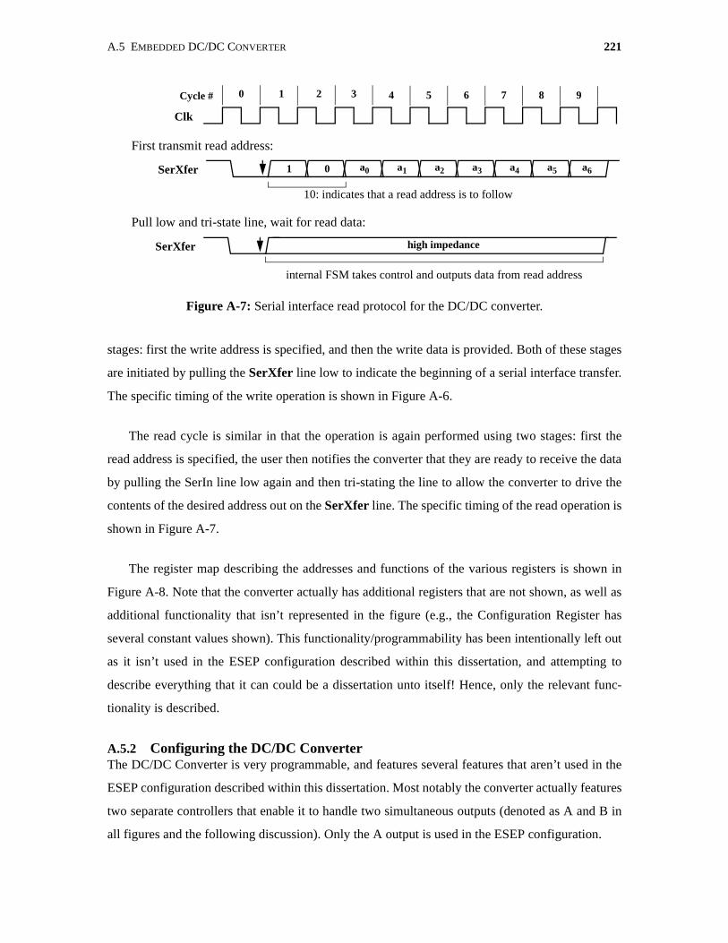
A.5 EMBEDDED DC/DC CONVERTER 221
stages: first the write address is specified, and then the write data is provided. Both of these stages
are initiated by pulling the SerXfer line low to indicate the beginning of a serial interface transfer.
The specific timing of the write operation is shown in Figure A-6.
The read cycle is similar in that the operation is again performed using two stages: first the
read address is specified, the user then notifies the converter that they are ready to receive the data
by pulling the SerIn line low again and then tri-stating the line to allow the converter to drive the
contents of the desired address out on the SerXfer line. The specific timing of the read operation is
shown in Figure A-7.
The register map describing the addresses and functions of the various registers is shown in
Figure A-8. Note that the converter actually has additional registers that are not shown, as well as
additional functionality that isn’t represented in the figure (e.g., the Configuration Register has
several constant values shown). This functionality/programmability has been intentionally left out
as it isn’t used in the ESEP configuration described within this dissertation, and attempting to
describe everything that it can could be a dissertation unto itself! Hence, only the relevant func-
tionality is described.
A.5.2 Configuring the DC/DC ConverterThe DC/DC Converter is very programmable, and features several features that aren’t used in the
ESEP configuration described within this dissertation. Most notably the converter actually features
two separate controllers that enable it to handle two simultaneous outputs (denoted as A and B in
all figures and the following discussion). Only the A output is used in the ESEP configuration.
Figure A-7: Serial interface read protocol for the DC/DC converter.
Clk
SerXfer
Cycle # 0 1 2 3 4 5 6 7 8 9
1 0 a0 a1 a2 a3 a4 a5 a6
SerXfer
First transmit read address:
Pull low and tri-state line, wait for read data:
10: indicates that a read address is to follow
high impedance
internal FSM takes control and outputs data from read address
222 APPENDIX A ENERGY SCALABLE ENCRYPTION PROCESSOR USER’S MANUAL
The basic operation of the DC/DC Converter was described in Section 4.3.3, and shown in
Figure 4-9. The Converter should be configured to gate the A/D converter output into the A con-
troller, which is then used to drive the PWM output. This requires the Configuration Register to be
set with the value 0x33, which enables both C1 and C2 as the core clocks of the converter (these
two signals should be driven from the same source so enabling both won’t cause any problems)
and gates the A/D output into the required controllers (we’re actually driving it into both A and B
but this won’t affect functionality). The key value that needs to be set is that of the ReferenceA and
ReferenceB registers (set both for completeness). The value stored in this register is added to the
output of the A/D to create an offset that is then multiplied by the appropriate scale values (stored
in the Scale Register) to form the resulting duty cycle error signal. The value stored in the Refer-
ence registers should be the 2’s-complement representation of the negative of the expected output
value of the A/D. The expected value will depend on the magnitude of the Vref (as the A/D’s out-
put is scaled from its value). A simple way to compute the required value is to use the formulae:
(A.1)
For example, if we had a Vref of 3V and wanted a 1.5V output we’d compute the value to be:
(A.2)
The other registers can be left at their default values, though if the need arises they can be changed
to improve stability/performance.
As alluded to earlier, the DC/DC Converter can operate using either an automatically updated
output duty cycle (if C1/C are enabled), or via a manual setting of the Duty Cycle registers. Note
that the manual setting will eliminate the voltage feedback regulation (as the feedback loop is
essentially disabled), thereby compromising the system’s ability to respond to variations in the
load. As such, it is recommended that the feedback not be disabled, and the system allowed to
operate using automatic updates of the duty cycle.
ReferenceA<7:0>Vdesired
Vref------------------
0x7F⋅ 1+=
ReferenceA<7:0>1.53
------- 0x7F⋅
1+
01000000 1+ 10111111 1+ 11000000 0xC0
=
= = = =

A.5 EMBEDDED DC/DC CONVERTER 223
0
Figure A-8: DC/DC Converter register map.
EnC2 EnC1 0 0 1 1
RefA: 8-bit value 2’s complement value representing the negative of the digital code representing the
EnC2: enables/disables (1/0) clock C2 as DC/DC converter core clockEnC1: enables/disables (1/0) clock C1 as DC/DC converter core clock
Configuration Register (Address = 0x00, default value = 0x33)07
RefA<7:0>
Reference A Register (Address = 0x01, default value = 0xCD)07
desired output value for the A output.
RefB: 8-bit value 2’s complement value representing the negative of the digital code representing the
RefB<7:0>
Reference B Register (Address = 0x02, default value = 0xCD)07
desired output value for the B output.
FBFreq: 8-bit value used to divide down the core clock into the feedback update clock
FBfreq<7:0>
Feedback Frequency Register (Address = 0x03, default value = 0x1C)07
(i.e., ffeedback = fcore / FBfreq7:0). Smaller value = faster updates in feedback loop.
ScaleB: 4-bit value used to scale the duty-cycle error signal (i.e., provides gain in feedback loop) for
ScaleA<3:0>
Scale Register (Address = 0x04, default value = 0x88)07
ScaleB<3:0>
the B output.
ScaleA: 4-bit value used to scale the duty-cycle error signal (i.e., provides gain in feedback loop) forthe A output.
DutyA: 12-bit value stored in two registers (upper and lower) that corresponds to the duty cycle used in the
DutyA<7:0>
Duty Cycle A Registers (Addresses = 0x09 (upper) and 0x07 (lower), default value = 0x28E)011
output PWM stages. Only the 10 MSB are used (i.e., DutyA<1:0> ignored) to specify the tap to be
8 7DutyA<11:8>
used in the virtual 1024-tap delay line. Note that this register can either be automatically updated if
either C1 or C2 is enabled in the Configuration Register, or manually set if they are both disabled.
DutyB: 12-bit value stored in two registers (upper and lower) that corresponds to the duty cycle used in the
DutyB<7:0>
Duty Cycle B Registers (Addresses = 0x09 (upper) and 0x07 (lower), default value = 0x200)011
output PWM stages. Only the 10 MSB are used (i.e., DutyA<1:0> ignored) to specify the tap to be
8 7DutyB<11:8>
used in the virtual 1024-tap delay line. Note that this register can either be automatically updated if
either C1 or C2 is enabled in the Configuration Register, or manually set if they are both disabled.

224 APPENDIX A ENERGY SCALABLE ENCRYPTION PROCESSOR USER’S MANUAL

225225225
Appendix B
DSRCP Instruction Set DefinitionThis appendix serves to give a detailed description of the DSRCP instruction set that was origi-
nally introduced in Section 5.3.1. The DSRCP ISA contains a total of 24 instructions, each of
which is shown in Table B-1, and then described in detail in the following text.
Opcode Mnemonic Opcode Mnemonic
00000 EC_DOUBLE rd rs0 rs2 10000 EC_MULT length
00001 GF_INV 10001 -reserved-
00010 GF_MULT 10010 MOD_MULT rd rs0 rs1 rs2
00011 MONT_RED 10011 -reserved-
00100 MONT_RED_A 10100 MOD rd rs0 rs1 rs2
00101 MONT_MULT 10101 -reserved-
00110 COMP rs0 rs1 10110 MOD_INV rd rs0
00111 GF_ADD rd rs0 rs1 10111 -reserved-
01000 ADD/SUB rd rs0 rs1 rs2 11000 -reserved-
01001 MOD_ADD rd rs0 rs1 rs2 11001 GF_EXP rd rs0
01010 SET_LENGTH length 11010 -reserved-
01011 MOD_SUB rd rs0 rs1 11011 MOD_EXP rd rs0 rs2 length
01100 -reserved- 11100 REG_CLEAR rd rs0
01101 EC_ADD rd rs0 rs1 rs2 11101 REG_MOVE rd rs0 rs2
01110 GF_INVMULT 11110 REG_LOAD rd
01111 -reserved- 11111 REG_UNLOAD rs1
Table B-1: DSRCP instruction set.
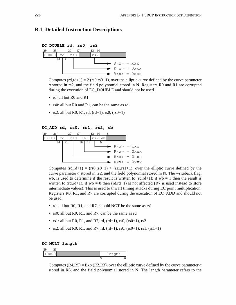
226 APPENDIX B DSRCP INSTRUCTION SET DEFINITION
B.1 Detailed Instruction Descriptions
EC_DOUBLE rd, rs0, rs2
Computes (rd,rd+1) = 2·(rs0,rs0+1), over the elliptic curve defined by the curve parametera stored in rs2, and the field polynomial stored in N. Registers R0 and R1 are corruptedduring the execution of EC_DOUBLE and should not be used.
• rd: all but R0 and R1
• rs0: all but R0 and R1, can be the same as rd
• rs2: all but R0, R1, rd, (rd+1), rs0, (rs0+1)
EC_ADD rd, rs0, rs1, rs2, wb
Computes (rd,rd+1) = (rs0,rs0+1) + (rs1,rs1+1), over the elliptic curve defined by thecurve parameter a stored in rs2, and the field polynomial stored in N. The writeback flag,wb, is used to determine if the result is written to (rd,rd+1): if wb = 1 then the result iswritten to (rd,rd+1), if wb = 0 then (rd,rd+1) is not affected (R7 is used instead to storeintermediate values). This is used to thwart timing attacks during EC point multiplication.Registers R0, R1, and R7 are corrupted during the execution of EC_ADD and should notbe used.
• rd: all but R0, R1, and R7, should NOT be the same as rs1
• rs0: all but R0, R1, and R7, can be the same as rd
• rs1: all but R0, R1, and R7, rd, (rd+1), rs0, (rs0+1), rs2
• rs2: all but R0, R1, and R7, rd, (rd+1), rs0, (rs0+1), rs1, (rs1+1)
EC_MULT length
Computes (R4,R5) = Exp·(R2,R3), over the elliptic curve defined by the curve parameter astored in R6, and the field polynomial stored in N. The length parameter refers to the
00000 rd rs0 rs229 25
24 21
20 17 12 10
R<x> = xxxR<x> = 0xxxR<x> = 0xxx
01101 rd rs1rs0 rs2 wb29 25
24 21
20 17
16 13
12 10
9
8
R<x> = xxxR<x> = 0xxxR<x> = 0xxxR<x> = 0xxx
10000 length29 25
9 0
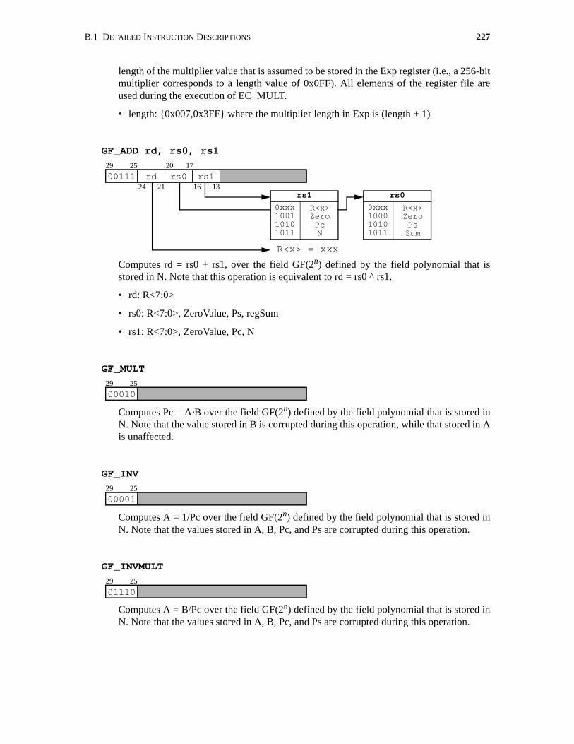
B.1 DETAILED INSTRUCTION DESCRIPTIONS 227
length of the multiplier value that is assumed to be stored in the Exp register (i.e., a 256-bitmultiplier corresponds to a length value of 0x0FF). All elements of the register file areused during the execution of EC_MULT.
• length: {0x007,0x3FF} where the multiplier length in Exp is (length + 1)
GF_ADD rd, rs0, rs1
Computes rd = rs0 + rs1, over the field GF(2n) defined by the field polynomial that isstored in N. Note that this operation is equivalent to rd = rs0 ^ rs1.
• rd: R<7:0>
• rs0: R<7:0>, ZeroValue, Ps, regSum
• rs1: R<7:0>, ZeroValue, Pc, N
GF_MULT
Computes Pc = A·B over the field GF(2n) defined by the field polynomial that is stored inN. Note that the value stored in B is corrupted during this operation, while that stored in Ais unaffected.
GF_INV
Computes A = 1/Pc over the field GF(2n) defined by the field polynomial that is stored inN. Note that the values stored in A, B, Pc, and Ps are corrupted during this operation.
GF_INVMULT
Computes A = B/Pc over the field GF(2n) defined by the field polynomial that is stored inN. Note that the values stored in A, B, Pc, and Ps are corrupted during this operation.
00111 rd rs1rs029 25
24 21
20 17
16 13
R<x> = xxx
0xxx100010101011
R<x>ZeroPsSum
rs0
0xxx100110101011
R<x>ZeroPcN
rs1
0001029 25
0000129 25
0111029 25
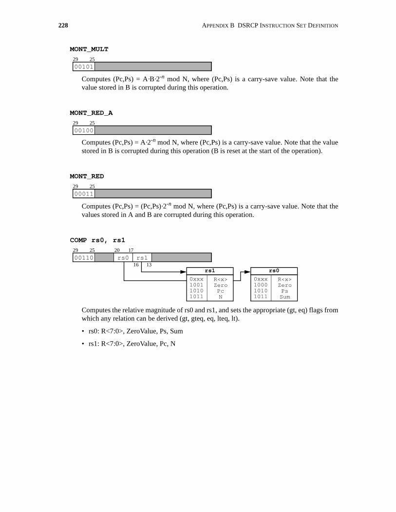
228 APPENDIX B DSRCP INSTRUCTION SET DEFINITION
MONT_MULT
Computes (Pc,Ps) = A·B·2-n mod N, where (Pc,Ps) is a carry-save value. Note that thevalue stored in B is corrupted during this operation.
MONT_RED_A
Computes (Pc,Ps) = A·2-n mod N, where (Pc,Ps) is a carry-save value. Note that the valuestored in B is corrupted during this operation (B is reset at the start of the operation).
MONT_RED
Computes (Pc,Ps) = (Pc,Ps)·2-n mod N, where (Pc,Ps) is a carry-save value. Note that thevalues stored in A and B are corrupted during this operation.
COMP rs0, rs1
Computes the relative magnitude of rs0 and rs1, and sets the appropriate (gt, eq) flags fromwhich any relation can be derived (gt, gteq, eq, lteq, lt).
• rs0: R<7:0>, ZeroValue, Ps, Sum
• rs1: R<7:0>, ZeroValue, Pc, N
0010129 25
0010029 25
0001129 25
00110 rs1rs029 25 20 17
16 13
0xxx100010101011
R<x>ZeroPsSum
rs0
0xxx100110101011
R<x>ZeroPcN
rs1
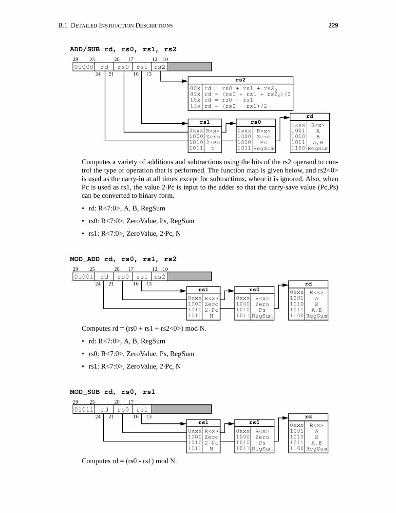
B.1 DETAILED INSTRUCTION DESCRIPTIONS 229
ADD/SUB rd, rs0, rs1, rs2
Computes a variety of additions and subtractions using the bits of the rs2 operand to con-trol the type of operation that is performed. The function map is given below, and rs2<0>is used as the carry-in at all times except for subtractions, where it is ignored. Also, whenPc is used as rs1, the value 2·Pc is input to the adder so that the carry-save value (Pc,Ps)can be converted to binary form.
• rd: R<7:0>, A, B, RegSum
• rs0: R<7:0>, ZeroValue, Ps, RegSum
• rs1: R<7:0>, ZeroValue, 2·Pc, N
MOD_ADD rd, rs0, rs1, rs2
Computes rd = (rs0 + rs1 + rs2<0>) mod N.
• rd: R<7:0>, A, B, RegSum
• rs0: R<7:0>, ZeroValue, Ps, RegSum
• rs1: R<7:0>, ZeroValue, 2·Pc, N
MOD_SUB rd, rs0, rs1
Computes rd = (rs0 - rs1) mod N.
01000 rd rs1rs0 rs229 25
24 21
20 17
16 13
12 10
00x01x10x11x
rd = rs0 + rs1 + rs20
rs2
rd = (rs0 + rs1 + rs20)/2rd = rs0 - rs1rd = (rs0 - rs1)/2
0xxx100010101011
R<x>ZeroPs
RegSum
rs0
0xxx100010101011
R<x>Zero2·PcN
rs1 0xxx100110101011
R<x>ABA,B
rd
1100 RegSum
01001 rd rs1rs0 rs229 25
24 21
20 17
16 13
12 10
0xxx100010101011
R<x>ZeroPs
RegSum
rs0
0xxx100010101011
R<x>Zero2·PcN
rs1 0xxx100110101011
R<x>ABA,B
rd
1100 RegSum
01011 rd rs1rs029 25
24 21
20 17
16 13
0xxx100010101011
R<x>ZeroPs
RegSum
rs0
0xxx100010101011
R<x>Zero2·PcN
rs1 0xxx100110101011
R<x>ABA,B
rd
1100 RegSum

230 APPENDIX B DSRCP INSTRUCTION SET DEFINITION
• rd: R<7:0>, A, B, RegSum
• rs0: R<7:0>, ZeroValue, Ps, RegSum
• rs1: R<7:0>, ZeroValue, 2·Pc, N
SET_LENGTH length
Configures the DSRCP’s length register from which all of the processor functions derivetheir operand sizes. The processor’s width is set equal to (length + 1).
• length: must be in the range {0x007,0x3FFF}
MOD_MULT rd, rs0, rs1, rs2
Computes rd = rs0·rs1 mod N using Montgomery Multiplication (MONT_MULT). TheMontgomery correction factor of 22n mod N is stored in rs2.
• rd: R<7:0>
• rs0: R<7:0>
• rs1: R<7:0>
• rs2: R<7:0>
MOD rd, rs0, rs1, rs2
Computes rd = (rs1·2n + rs0) mod N using Montgomery reduction (MONT_RED). TheMontgomery correction factor of 22n mod N is stored in rs2, and the current width of theprocessor must be a multiple of 32 (i.e., the last invocation of SET_LENGTH(n) must sat-isfy (n+1) mod 32 = 0).
• rd: R<7:0>
• rs0: R<7:0>
01010 length29 25
9 0
10010 rd rs1rs0 rs229 25
24 21
20 17
16 13
12 10
R<x> = xxxR<x> = 0xxxR<x> = 0xxxR<x> = 0xxx
10100 rd rs1rs0 rs229 25
24 21
20 17
16 13
12 10
R<x> = xxxR<x> = 0xxxR<x> = 0xxxR<x> = 0xxx

B.1 DETAILED INSTRUCTION DESCRIPTIONS 231
• rs1: R<7:0>
• rs2: R<7:0>
MOD_INV rd, rs0
Computes rd = (1 / rs0) mod N using a modified form of the binary extended euclideanalgorithm. Although registers R0, R1, R2, and R3 are corrupted during the execution ofMOD_INV they can be used for rd and rs0 so long as the user understands that, in the caseof rs0, its value will no longer be valid at the completion of the operation.
• rd: R<7:0>
• rs0: R<7:0>
MOD_EXP rd, rs0, rs2, length
Computes rd = rs0Exp mod N using Montgomery exponentiation. The Montgomery cor-rection factor of 22n mod N is stored in rs2, and the length input refers to the length of theexponent value that is assumed to be stored in the Exp register (i.e., if it is a 512-bit expo-nent then the length value is 0x1FF). Registers R0, R1, R2, and R3 are corrupted duringthe execution of MOD_EXP so they should not be used for rd and rs2, but R1, R2, and R3could be used for rs0. At the completion of the MOD_EXP operation, R0 = 2n mod N, R1= rs0·2n mod N, R2 = rs02·2n mod N, and R3 = rs03·2n mod N.
• rd: R<7:4>
• rs0: R<7:1>
• rs2: R<7:4>
• length: must be in {0x000,0x3FF} where the exponent length in Exp is (length + 1)
10110 rd rs029 25
24 21
20 17
R<x> = 0xxxR<x> = 0xxx
11011 rd rs0 rs2 length29 25
24 21
20 17 12 10
9 0R<x> = xxxR<x> = 0xxxR<x> = 0xxx
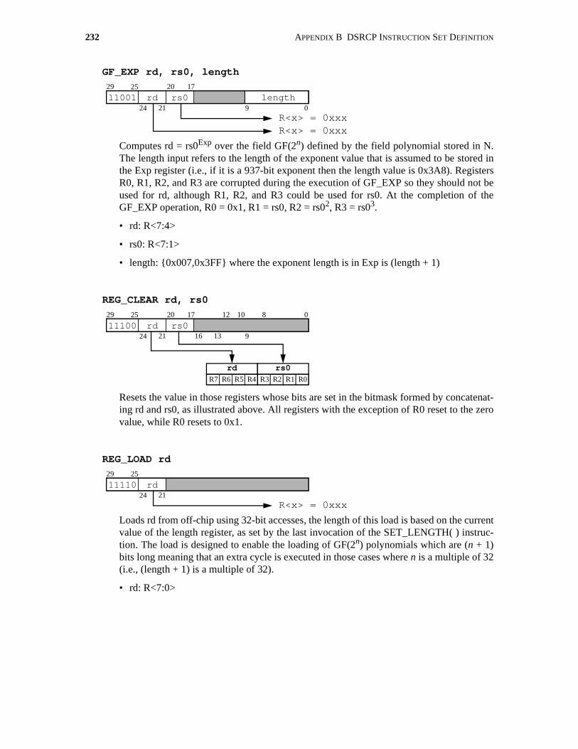
232 APPENDIX B DSRCP INSTRUCTION SET DEFINITION
GF_EXP rd, rs0, length
Computes rd = rs0Exp over the field GF(2n) defined by the field polynomial stored in N.The length input refers to the length of the exponent value that is assumed to be stored inthe Exp register (i.e., if it is a 937-bit exponent then the length value is 0x3A8). RegistersR0, R1, R2, and R3 are corrupted during the execution of GF_EXP so they should not beused for rd, although R1, R2, and R3 could be used for rs0. At the completion of theGF_EXP operation, R0 = 0x1, R1 = rs0, R2 = rs02, R3 = rs03.
• rd: R<7:4>
• rs0: R<7:1>
• length: {0x007,0x3FF} where the exponent length is in Exp is (length + 1)
REG_CLEAR rd, rs0
Resets the value in those registers whose bits are set in the bitmask formed by concatenat-ing rd and rs0, as illustrated above. All registers with the exception of R0 reset to the zerovalue, while R0 resets to 0x1.
REG_LOAD rd
Loads rd from off-chip using 32-bit accesses, the length of this load is based on the currentvalue of the length register, as set by the last invocation of the SET_LENGTH( ) instruc-tion. The load is designed to enable the loading of GF(2n) polynomials which are (n + 1)bits long meaning that an extra cycle is executed in those cases where n is a multiple of 32(i.e., (length + 1) is a multiple of 32).
• rd: R<7:0>
11001 rd rs0 length29 25
24 21
20 17
9 0R<x> = 0xxxR<x> = 0xxx
11100 rd rs029 25
24 21
20 17
16 13
12 10
9
08
R7 R6 R5 R4 R3 R2 R1 R0
rs0rd
11110 rd29 25
24 21R<x> = 0xxx
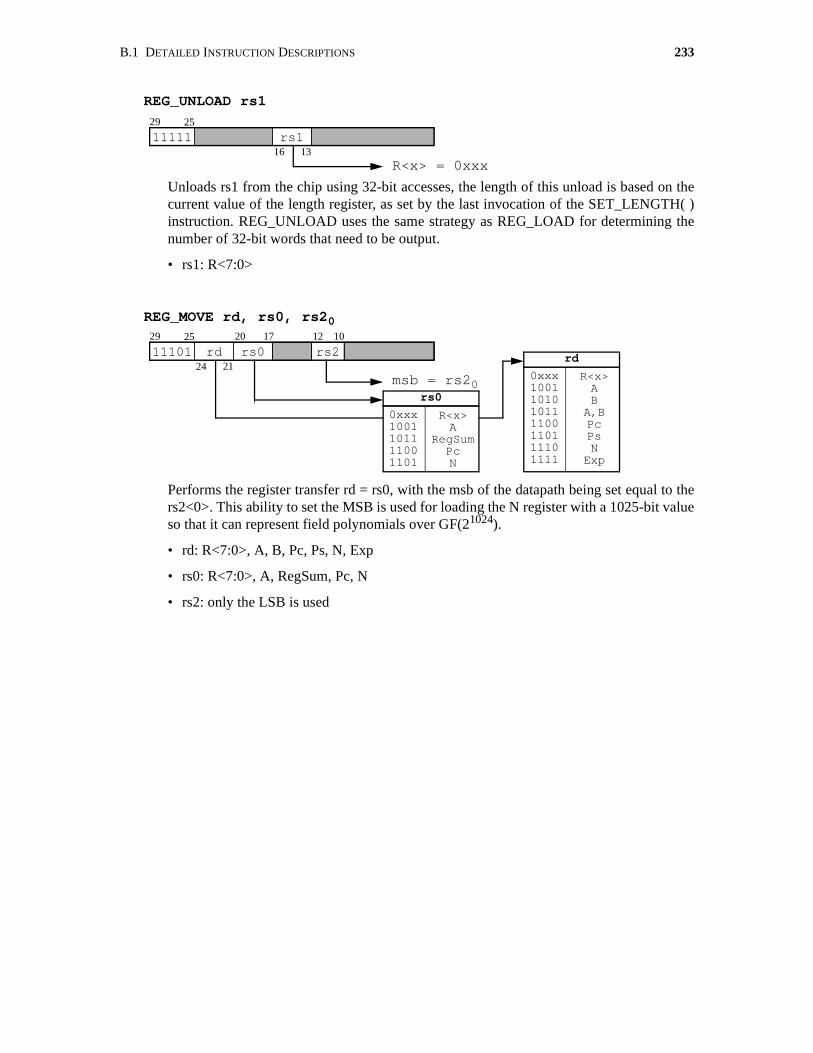
B.1 DETAILED INSTRUCTION DESCRIPTIONS 233
REG_UNLOAD rs1
Unloads rs1 from the chip using 32-bit accesses, the length of this unload is based on thecurrent value of the length register, as set by the last invocation of the SET_LENGTH( )instruction. REG_UNLOAD uses the same strategy as REG_LOAD for determining thenumber of 32-bit words that need to be output.
• rs1: R<7:0>
REG_MOVE rd, rs0, rs20
Performs the register transfer rd = rs0, with the msb of the datapath being set equal to thers2<0>. This ability to set the MSB is used for loading the N register with a 1025-bit valueso that it can represent field polynomials over GF(21024).
• rd: R<7:0>, A, B, Pc, Ps, N, Exp
• rs0: R<7:0>, A, RegSum, Pc, N
• rs2: only the LSB is used
11111 rs129 25
16 13R<x> = 0xxx
11101 rd rs0 rs229 25
24 21
20 17 12 10
msb = rs20
0xxx1001101111001101
R<x>A
RegSumPcN
rs0
0xxx1001101010111100110111101111
R<x>ABA,BPcPsNExp
rd

234 APPENDIX B DSRCP INSTRUCTION SET DEFINITION

235235235
Appendix C
DSRCP User’s ManualThis appendix serves as a general user’s manual for using the Domain Specific Reconfigurable
Processor described in Chapter 5.
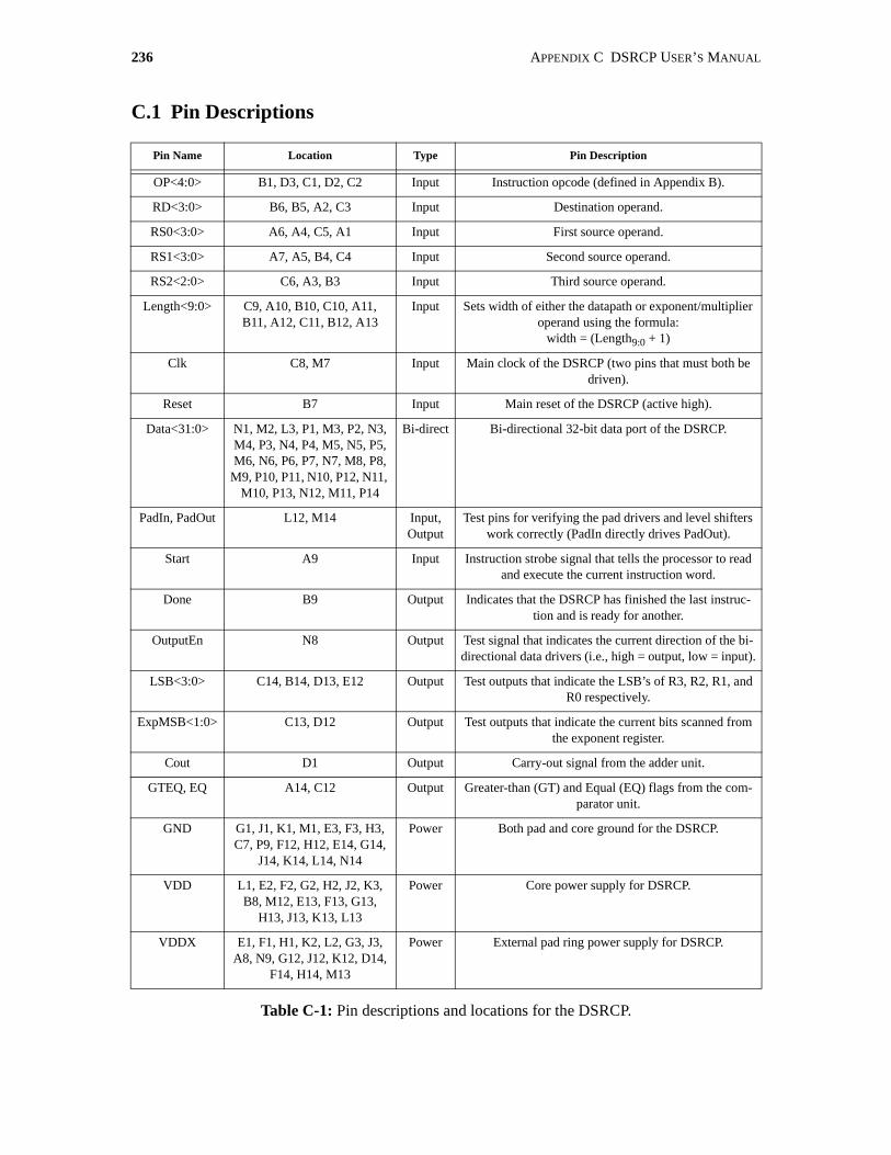
236 APPENDIX C DSRCP USER’S MANUAL
C.1 Pin Descriptions
Pin Name Location Type Pin Description
OP<4:0> B1, D3, C1, D2, C2 Input Instruction opcode (defined in Appendix B).
RD<3:0> B6, B5, A2, C3 Input Destination operand.
RS0<3:0> A6, A4, C5, A1 Input First source operand.
RS1<3:0> A7, A5, B4, C4 Input Second source operand.
RS2<2:0> C6, A3, B3 Input Third source operand.
Length<9:0> C9, A10, B10, C10, A11, B11, A12, C11, B12, A13
Input Sets width of either the datapath or exponent/multiplier operand using the formula:
width = (Length9:0 + 1)
Clk C8, M7 Input Main clock of the DSRCP (two pins that must both be driven).
Reset B7 Input Main reset of the DSRCP (active high).
Data<31:0> N1, M2, L3, P1, M3, P2, N3, M4, P3, N4, P4, M5, N5, P5, M6, N6, P6, P7, N7, M8, P8,
M9, P10, P11, N10, P12, N11, M10, P13, N12, M11, P14
Bi-direct Bi-directional 32-bit data port of the DSRCP.
PadIn, PadOut L12, M14 Input, Output
Test pins for verifying the pad drivers and level shifters work correctly (PadIn directly drives PadOut).
Start A9 Input Instruction strobe signal that tells the processor to read and execute the current instruction word.
Done B9 Output Indicates that the DSRCP has finished the last instruc-tion and is ready for another.
OutputEn N8 Output Test signal that indicates the current direction of the bi-directional data drivers (i.e., high = output, low = input).
LSB<3:0> C14, B14, D13, E12 Output Test outputs that indicate the LSB’s of R3, R2, R1, and R0 respectively.
ExpMSB<1:0> C13, D12 Output Test outputs that indicate the current bits scanned from the exponent register.
Cout D1 Output Carry-out signal from the adder unit.
GTEQ, EQ A14, C12 Output Greater-than (GT) and Equal (EQ) flags from the com-parator unit.
GND G1, J1, K1, M1, E3, F3, H3, C7, P9, F12, H12, E14, G14,
J14, K14, L14, N14
Power Both pad and core ground for the DSRCP.
VDD L1, E2, F2, G2, H2, J2, K3, B8, M12, E13, F13, G13,
H13, J13, K13, L13
Power Core power supply for DSRCP.
VDDX E1, F1, H1, K2, L2, G3, J3, A8, N9, G12, J12, K12, D14,
F14, H14, M13
Power External pad ring power supply for DSRCP.
Table C-1: Pin descriptions and locations for the DSRCP.
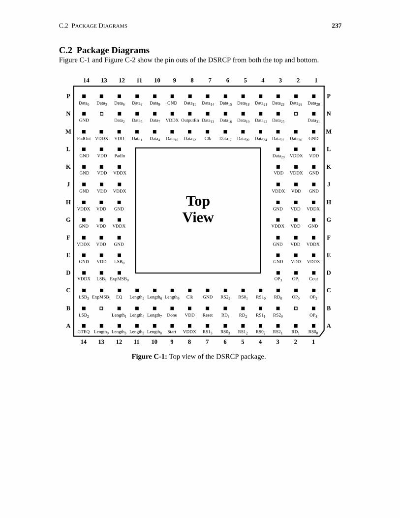
C.2 PACKAGE DIAGRAMS 237
C.2 Package DiagramsFigure C-1 and Figure C-2 show the pin outs of the DSRCP from both the top and bottom.
GND
234569 710 8111213 1
B
C
D
E
F
G
H
J
K
L
M
N
P
TopView
Figure C-1: Top view of the DSRCP package.
14
A
Data11 Data14 Data15 Data18 Data21 Data23 Data26Data8 Data9 Data28Data3 Data6Data0
VDDX OutputEn Data13 Data16 Data19 Data22 Data25Data5 Data7 Data31Data2GND
Data10 Data12 Clk Data17 Data20 Data24 Data27 Data30Data1 Data4 GNDVDDX VDDPadOut
Data29 VDDX VDDVDD PadInGND
VDD VDDX GNDVDD VDDXGND
VDDX VDD GNDVDD VDDXGND
GND VDD VDDXVDD GNDVDDX
VDDX VDD GNDVDD VDDXGND
GND VDD VDDXVDD GNDVDDX
GND VDD VDDXVDD LSB0GND
OP3 OP1 CoutLSB1 ExpMSB0VDDX
Length9 Clk GND RS22 RS01 RS10 RD0 OP0Length2 Length6 OP2ExpMSB1 EQLSB3
Done VDD Reset RD3 RD2 RS11 RS20Length4 Length7 OP4Length1LSB2
Start VDDX RS13 RS03 RS12 RS02 RS21 RD1Length5 Length8 RS00Length0 Length3GTEQ
234569 710 8111213 114
B
C
D
E
F
G
H
J
K
L
M
N
P
A

238 APPENDIX C DSRCP USER’S MANUAL
C.3 Basic OperationThe DSRCP operates using a simple handshaking interface consisting of the Start/Done signals.
This is pseudo-asynchronous in the sense that the delay between the start and finish of the instruc-
tion execution is not fixed, but can vary depending on the operation performed, and operand values
used. However, all signal generation and data latching is done synchronous to the main Clk signal.
The basic operation of the processor is then a simple matter of assembling the appropriate
instruction word (using the assembly guidelines and codings given in Appendix B), asserting the
Start signal, and then waiting for the Done signal to be asserted, indicating that the instruction has
GND
2 3 4 5 6 97 108 11 12 131
B
C
D
E
F
G
H
J
K
L
M
N
P
BottomView
Figure C-2: Bottom view of the DSRCP package.
14
A
Data11Data14Data15Data18Data21Data23Data26 Data8Data9Data28 Data3Data6 Data0
VDDXOutputEnData13Data16Data19Data22Data25 Data5Data7Data31 Data2 GND
Data10Data12ClkData17Data20Data24Data27Data30 Data1Data4GND VDDXVDD PadOut
Data29VDDXVDD VDDPadIn GND
VDDVDDXGND VDDVDDX GND
VDDXVDDGND VDDVDDX GND
GNDVDDVDDX VDDGND VDDX
VDDXVDDGND VDDVDDX GND
GNDVDDVDDX VDDGND VDDX
GNDVDDVDDX VDDLSB0 GND
OP3OP1Cout LSB1ExpMSB0 VDDX
Length9ClkGNDRS22RS01RS10RD0OP0 Length2Length6OP2 ExpMSB1EQ LSB3
DoneVDDResetRD3RD2RS11RS20 Length4Length7OP4 Length1 LSB2
StartVDDXRS13RS03RS12RS02RS21RD1 Length5Length8RS00 Length0Length3 GTEQ
2 3 4 5 6 97 108 11 12 131 14
B
C
D
E
F
G
H
J
K
L
M
N
P
A
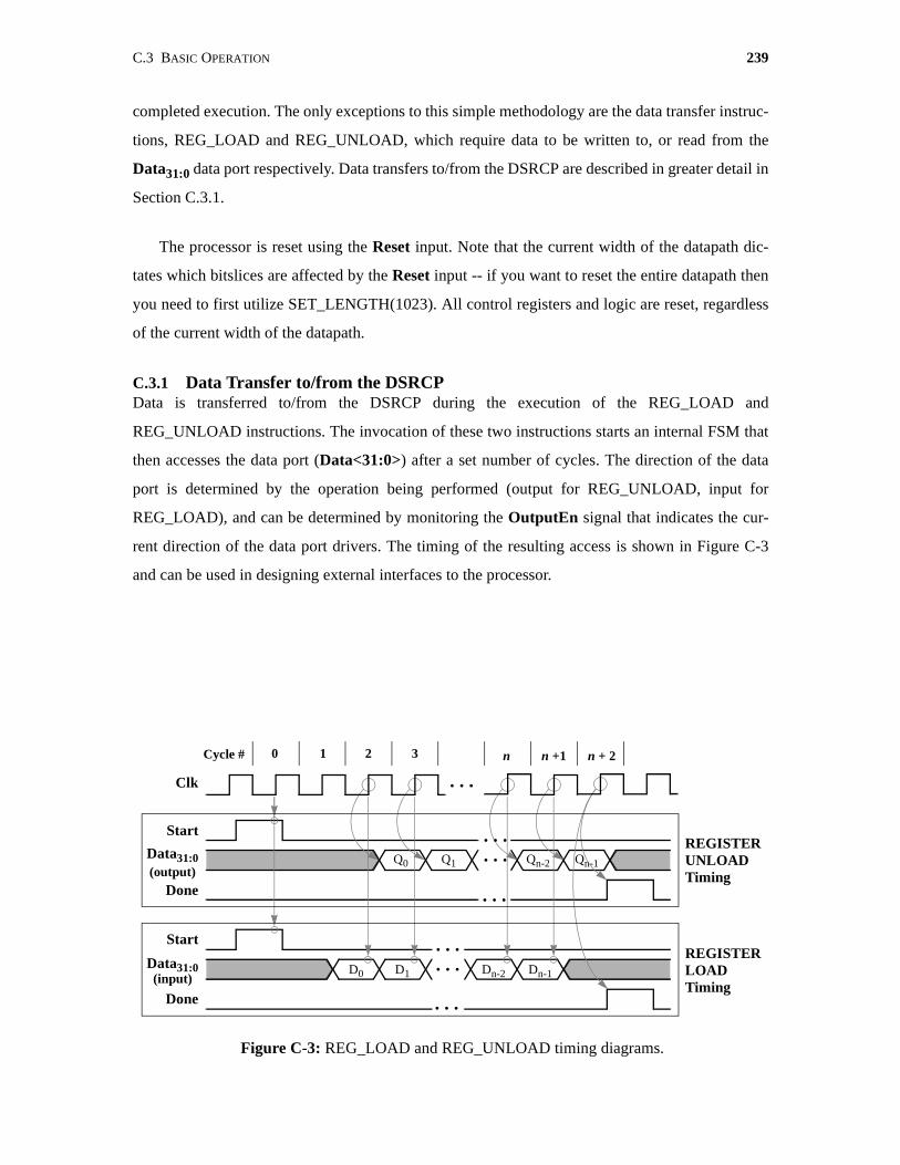
C.3 BASIC OPERATION 239
completed execution. The only exceptions to this simple methodology are the data transfer instruc-
tions, REG_LOAD and REG_UNLOAD, which require data to be written to, or read from the
Data31:0 data port respectively. Data transfers to/from the DSRCP are described in greater detail in
Section C.3.1.
The processor is reset using the Reset input. Note that the current width of the datapath dic-
tates which bitslices are affected by the Reset input -- if you want to reset the entire datapath then
you need to first utilize SET_LENGTH(1023). All control registers and logic are reset, regardless
of the current width of the datapath.
C.3.1 Data Transfer to/from the DSRCPData is transferred to/from the DSRCP during the execution of the REG_LOAD and
REG_UNLOAD instructions. The invocation of these two instructions starts an internal FSM that
then accesses the data port (Data<31:0>) after a set number of cycles. The direction of the data
port is determined by the operation being performed (output for REG_UNLOAD, input for
REG_LOAD), and can be determined by monitoring the OutputEn signal that indicates the cur-
rent direction of the data port drivers. The timing of the resulting access is shown in Figure C-3
and can be used in designing external interfaces to the processor.
Figure C-3: REG_LOAD and REG_UNLOAD timing diagrams.
Clk
Start
Data31:0
Done
Q0
Cycle # 0 1 2 3 n n +1 n + 2
Q1 Qn-2 Qn-1. . .
. . .
. . .
D0 D1 Dn-2 Dn-1. . .
. . .
. . .Start
Data31:0
Done
. . .
REGISTERUNLOADTiming
REGISTERLOADTiming
(output)
(input)

240 APPENDIX C DSRCP USER’S MANUAL
241241241
Appendix D
SHA-1 Circuit SchematicsAs mentioned in Section 5.7.5, the Secure Hash Algorithm (rev. 1) function was designed down to
the transistor level but was not included in the final layout of the DSRCP due to time limitations
imposed by the fabrications schedules and tapeout deadlines. Hence, we’ve provided a complete
set of schematics (down to the basic logical gates) for the SHA-1 Engine so that others interested
in the design have a reference design for their use. We encourage others to utilize this design in
their own work and only ask that some reference to the source of the design be included in the
design documentation.

242 APPENDIX D SHA-1 CIRCUIT SCHEMATICS
D.1 Complete SHA-1 Circuit Schematics
Figure D-1: Top-level SHA-1 engine circuit schematic.
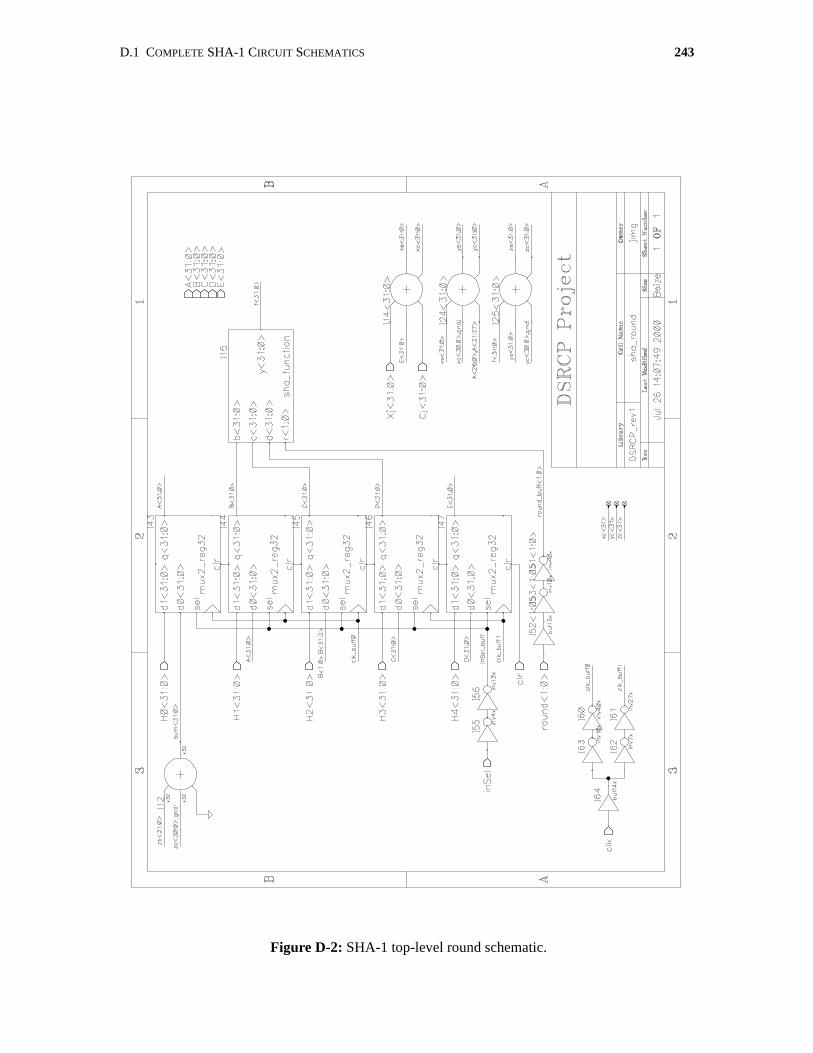
D.1 COMPLETE SHA-1 CIRCUIT SCHEMATICS 243
Figure D-2: SHA-1 top-level round schematic.
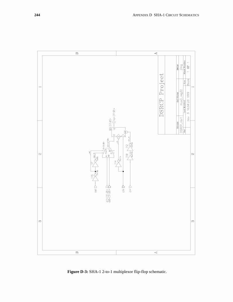
244 APPENDIX D SHA-1 CIRCUIT SCHEMATICS
Figure D-3: SHA-1 2-to-1 multiplexor flip-flop schematic.
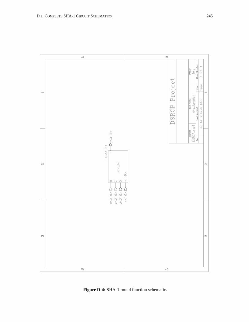
D.1 COMPLETE SHA-1 CIRCUIT SCHEMATICS 245
Figure D-4: SHA-1 round function schematic.

246 APPENDIX D SHA-1 CIRCUIT SCHEMATICS
Figure D-5: SHA-1 round function bitslice schematic.
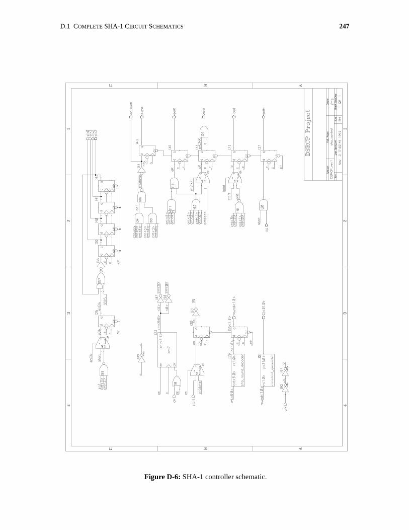
D.1 COMPLETE SHA-1 CIRCUIT SCHEMATICS 247
Figure D-6: SHA-1 controller schematic.
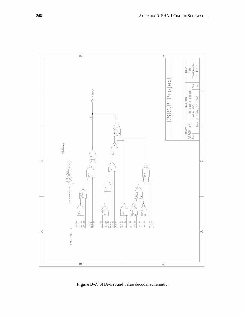
248 APPENDIX D SHA-1 CIRCUIT SCHEMATICS
Figure D-7: SHA-1 round value decoder schematic.

D.1 COMPLETE SHA-1 CIRCUIT SCHEMATICS 249
Figure D-8: SHA-1 yi constant generator schematic.
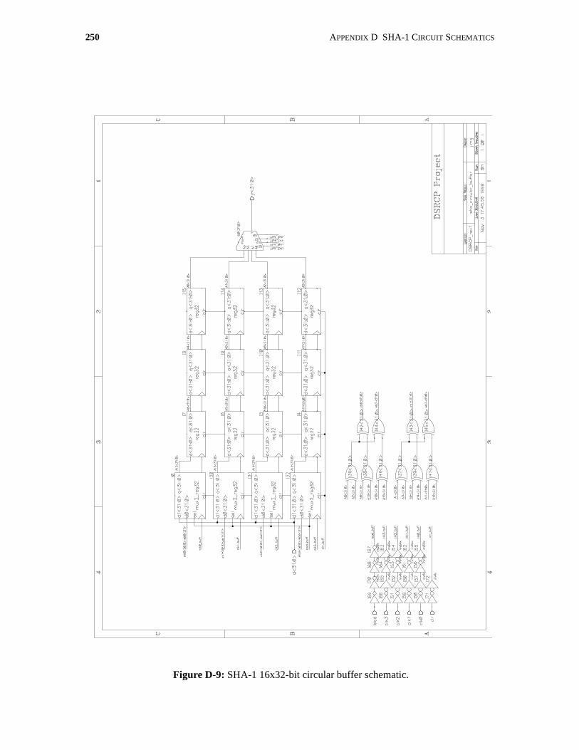
250 APPENDIX D SHA-1 CIRCUIT SCHEMATICS
Figure D-9: SHA-1 16x32-bit circular buffer schematic.
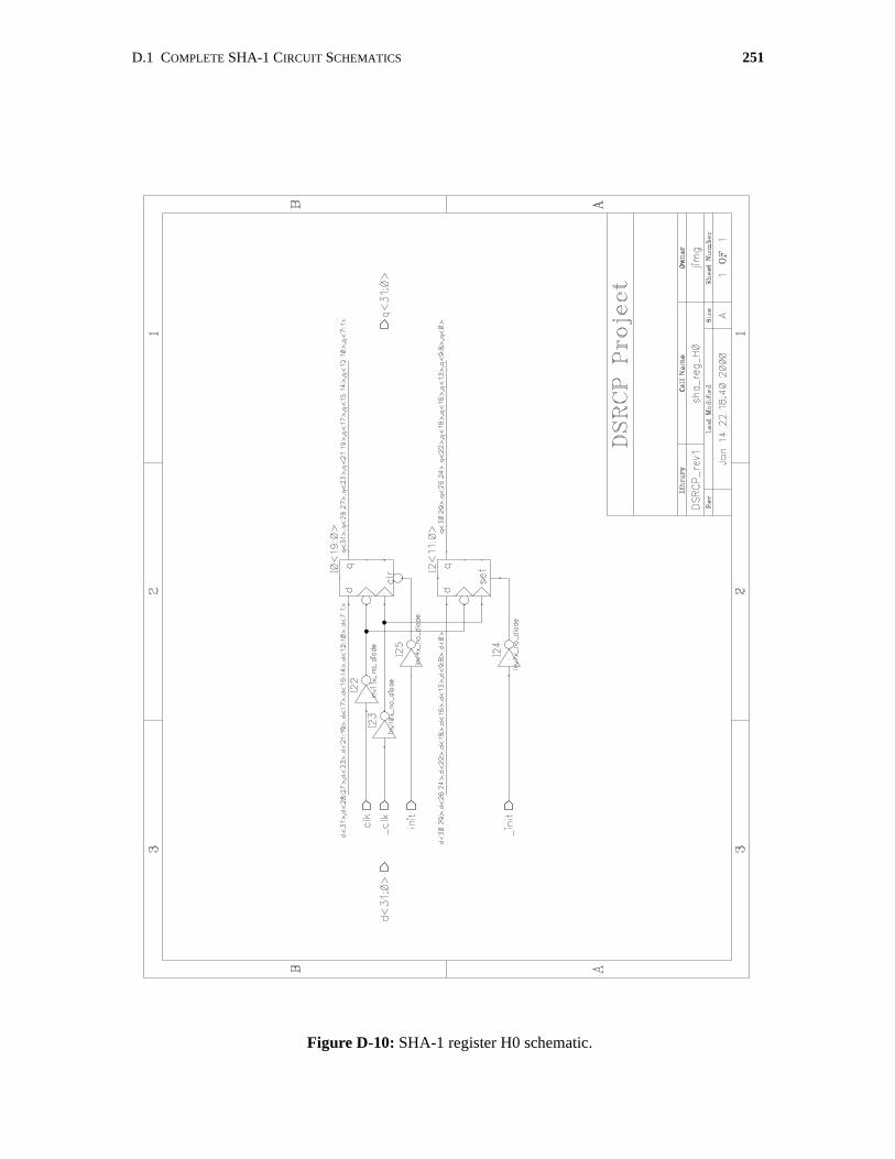
D.1 COMPLETE SHA-1 CIRCUIT SCHEMATICS 251
Figure D-10: SHA-1 register H0 schematic.
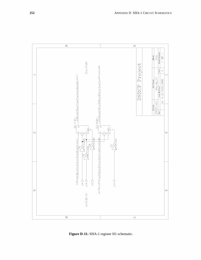
252 APPENDIX D SHA-1 CIRCUIT SCHEMATICS
Figure D-11: SHA-1 register H1 schematic.

D.1 COMPLETE SHA-1 CIRCUIT SCHEMATICS 253
Figure D-12: SHA-1 register H2 schematic.

254 APPENDIX D SHA-1 CIRCUIT SCHEMATICS
Figure D-13: SHA-1 register H3 schematic.

D.1 COMPLETE SHA-1 CIRCUIT SCHEMATICS 255
Figure D-14: SHA-1 register H4 schematic.
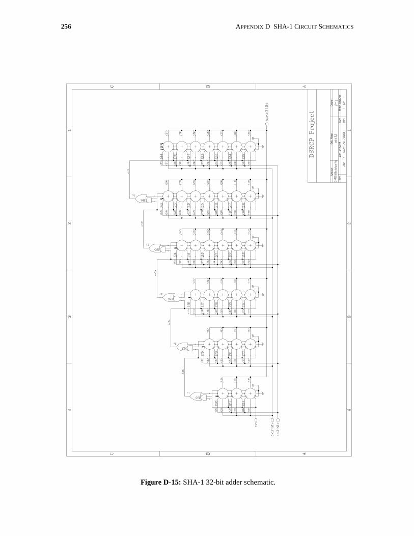
256 APPENDIX D SHA-1 CIRCUIT SCHEMATICS
Figure D-15: SHA-1 32-bit adder schematic.