Embed Size (px)
Citation preview
Engineer-to-Engineer Note EE-178
a
Technical notes on using Analog Devices DSPs, processors and development toolsContact our technical support at [email protected] and at [email protected] visit our on-line resources http://www.analog.com/ee-notes and http://www.analog.com/processors
The ADSP-TS101S TigerSHARC® On-chip SDRAM Controller Contributed by Maikel Kokaly-Bannourah & Robert Hoffmann Rev 2 – December 19, 2003
Copyright 2003, Analog Devices, Inc. All rights reserved. Analog Devices assumes no responsibility for customer product design or the use or application of customers’ products or for any infringements of patents or rights of others which may result from Analog Devices assistance. All trademarks and logos are property of their respective holders. Information furnished by Analog Devices Applications and Development Tools Engineers is believed to be accurate and reliable, however no responsibility is assumed by Analog Devices regarding technical accuracy and topicality of the content provided in Analog Devices’ Engineer-to-Engineer Notes.
1 Introduction In systems where a Digital Signal Processor (DSP) is used to address Synchronous Dynamic Random Access Memory (SDRAM), additional hardware and software is needed to handle the multiplexed row and column addressing, as well as the refresh and precharge requirements of the SDRAM. The ADSP-TS101S TigerSHARC® processor uses a hardware intensive solution, an on-chip SDRAM controller.
This Engineer-to-Engineer Note introduces the ADSP-TS101S on-chip SDRAM controller‘s characteristics. The internal signal chain is shown with the necessary address-mapping scheme. The command truth table gives detailed information about execution in the SDRAM. The important power-up sequence summarizes detail information to start successful designs. A timing overview demonstrates the performance for different access modes. For basic understanding of SDRAM memories, refer to “The ABC of SDRAMemory (EE-126)” [3].
a
2 Table of Contents
1 Introduction ............................................................................................................................................................................1
2 Table of Contents....................................................................................................................................................................2
3 Signal Chain of SDRAM ........................................................................................................................................................4
4 On-Chip Controller Architecture .........................................................................................................................................5 4.1 Controller Command Interface .....................................................................................................................................5 4.2 TigerSHARC Output FIFO...........................................................................................................................................5 4.3 Controller Address Multiplexer ....................................................................................................................................5 4.4 Controller Data Delay Buffer .......................................................................................................................................5 4.5 SDRAM Types .............................................................................................................................................................5
5 Command Coding...................................................................................................................................................................6 5.1 Controller’s Pin Definition ...........................................................................................................................................6 5.2 Controller Command Truth Table ................................................................................................................................6 5.3 Setup and Hold Times ..................................................................................................................................................7 5.4 Simplified State Diagram..............................................................................................................................................7
6 SDRAM Controller Properties..............................................................................................................................................9 6.1 Address Mapping Scheme ............................................................................................................................................9 6.2 TigerSHARC SDRAM Bank Select (~MSSD) ..........................................................................................................10 6.3 Burst Stop (BST) ........................................................................................................................................................10 6.4 Data Mask Function ([H:L]DQM)..............................................................................................................................11 6.5 SDRAM Bank Select ..................................................................................................................................................11 6.6 Controller Address 10 (SDA10) .................................................................................................................................12 6.7 Burst Mode .................................................................................................................................................................12 6.8 Precharge All (PREA) ................................................................................................................................................12 6.9 Circular Access...........................................................................................................................................................12 6.10 Auto-Refresh (REF)..................................................................................................................................................12 6.11 Self-Refresh (SREF).................................................................................................................................................12 6.12 Mode Register Set (MRS).........................................................................................................................................13
7 SDRAM Programming.........................................................................................................................................................14 7.1 SYSCON Register ......................................................................................................................................................14 7.2 SDRCON Register......................................................................................................................................................14 7.3 SDRAM Mode of Operation ......................................................................................................................................16 7.4 ADSP-TS101S EZ-KIT Lite.......................................................................................................................................16 7.5 SDRAM Setting Overview .........................................................................................................................................17
8 Power-up Sequence...............................................................................................................................................................18 8.1 Hardware Initialization ...............................................................................................................................................18 8.2 Software Initialization ................................................................................................................................................18 8.3 SDRAM Initialization Example..................................................................................................................................19 8.4 SDRAM Interface After Reset....................................................................................................................................19
9 DMA Transfers .....................................................................................................................................................................20 9.1 Internal Memory and SDRAM ...................................................................................................................................20 9.2 External Device and SDRAM (FLY-BY) ..................................................................................................................20
10 SDRAM Interface in Host Mode.......................................................................................................................................22
The ADSP-TS101S TigerSHARC® On-chip SDRAM Controller (EE-178) Page 2 of 44
a 11 Multiprocessing...................................................................................................................................................................24
11.1 Command Decoding .................................................................................................................................................24 11.2 MRS Decoding .........................................................................................................................................................24 11.3 REF Decoding ..........................................................................................................................................................24 11.4 SREF Decoding ........................................................................................................................................................24 11.5 Bus Transition Cycle ................................................................................................................................................24
12 SDRAM and Booting..........................................................................................................................................................26 12.1 Loader Kernel ...........................................................................................................................................................26 12.2 Booting Modes .........................................................................................................................................................26
13 SDRAM Interface Throughput .........................................................................................................................................27 13.1 Sequential Reads without Interruption .....................................................................................................................28 13.2 Non Sequential Reads without Interruption..............................................................................................................29 13.3 Sequential Reads with minimum Interruption ..........................................................................................................30 13.4 Sequential Writes without Interruption.....................................................................................................................31 13.5 Non Sequential Writes without Interruption.............................................................................................................32 13.6 Sequential Writes with minimum Interruption .........................................................................................................33 13.7 Reads between Page/Bank........................................................................................................................................34 13.8 Writes between Page/Bank .......................................................................................................................................35 13.9 Minimum Read to Write Interval..............................................................................................................................36 13.10 Minimum Write to Read Interval............................................................................................................................37 13.11 Chained DMA Transfers.........................................................................................................................................38 13.12 Auto-Refresh ..........................................................................................................................................................39 13.13 Self-Refresh and Host Accesses .............................................................................................................................40 13.14 SDRAM Performance Table...................................................................................................................................42
14 Optimizing SDRAM Performance ....................................................................................................................................43 14.1 External Buffering ....................................................................................................................................................43 14.2 Using PC Modules....................................................................................................................................................44
...............................................................................................................44 14.3 General Rules for Optimized Performance
............................................................................................................................................................................44 15 References
...............................................................................................................................................................44 16 Document History
The ADSP-TS101S TigerSHARC® On-chip SDRAM Controller (EE-178) Page 3 of 44
a
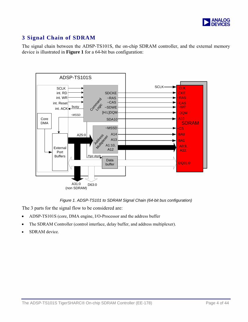
3 Signal Chain of SDRAM The signal chain between the ADSP-TS101S, the on-chip SDRAM controller, and the external memory device is illustrated in Figure 1 for a 64-bit bus configuration:
SDCKE~RAS~CAS
~SDWE[H:L]DQM
SDA10
SCLKint. RDint. WR
int. Resetint. ACK Com
mand
Logic
ADSP-TS101S
Addre
ssMult
iplex
er
A1:10,A12
A13A14
~MSSD
D63:0
ExternalPort
Buffers
CoreDMA
A31:0(non SDRAM)
Databuffer
busy
~MSSD
Pipe depth
A25:0
CLKCKE
~RAS~CAS~WE
DQM
~CS
DQ31:0
BA0
A0:9,A12,
SDRAM
BA1
A10
SCLK
Figure 1. ADSP-TS101 to SDRAM Signal Chain (64-bit bus configuration)
The 3 parts for the signal flow to be considered are:
• ADSP-TS101S (core, DMA engine, I/O-Processor and the address buffer
• The SDRAM Controller (control interface, delay buffer, and address multiplexer).
• SDRAM device.
The ADSP-TS101S TigerSHARC® On-chip SDRAM Controller (EE-178) Page 4 of 44
a
4 On-Chip Controller Architecture The synchronous interface between the ADSP-TS101S and the on-chip controller can be described in 4 basic parts:
4.1 Controller Command Interface
Because of the 2 different timing protocols, the internal TigerSHARC commands are converted to comply with the JEDEC standard for SDRAMs. The external clock, 100 MHz maximum, is used for synchronous operation. The TigerSHARC’s internal request lines or strobes are used to access the SDRAM with pulsed commands. The controller’s internal ACK line inserts variable wait states to the DSP during overhead cycles, caused by DRAM technology.
4.2 TigerSHARC Output FIFO
The TigerSHARC’s output FIFO is active for external port addresses like SDRAM. With the FIFO depth 6, address pipelining for high-speed non-sequential read operations (CAS latency=3) is supported without performance losses.
4.3 Controller Address Multiplexer
Every first read or write action is issued in multiplexed mode. A maximum of 8192 rows (64-bit bus configuration) and 16384 rows (32-bit bus configuration) within 1024 columns can be addressed.
4.4 Controller Data Delay Buffer
If systems incorporate a heavy busload, an additional data buffers is used to decouple the input from the capacitive load. This delay buffer in conjunction with an external buffer for SDRAM control and address lines reduces additional logic to a minimum.
4.5 SDRAM Types
The ADSP-TS101S on-chip SDRAM controller interface supports various LVTTL SDRAM devices depending on size and internal organization (I/O capability, number of rows, and page size). The following table summarizes all the supported types:
Size I/O capability Row x Page Size I/O capability Row x Page 1M x 16 2k x 256 8M x 32 8k x 2562M x 8 2k x 512 16M x 16 8k x 51216 Mbits 4M x 4 2k x 1024
256 Mbits 32M x 8 8k x 1024
2M x 32 2k x 256 8M x 32 8k x 2564M x 16 4k x 256 16M x 16 8k x 5128M x 8 4k x 512
512 Mbits 32M x 8 8k x 1024
64 Mbits
16M x 4 4k x 10244M x 32 4k x 2568M x 16 4k x 512128 Mbits 16M x 8 4k x 1024
The ADSP-TS101S TigerSHARC® On-chip SDRAM Controller (EE-178) Page 5 of 44
a
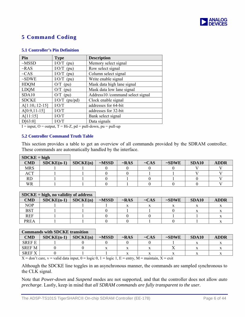
5 Command Coding
5.1 Controller’s Pin Definition
Pin Type Description ~MSSD I/O/T (pu) Memory select signal ~RAS I/O/T (pu) Row select signal ~CAS I/O/T (pu) Column select signal ~SDWE I/O/T (pu) Write enable signal HDQM O/T (pu) Mask data high lane signal LDQM O/T (pu) Mask data low lane signal SDA10 O/T (pu) Address10 /command select signal SDCKE I/O/T (pu/pd) Clock enable signal A[1:10,:12-15] I/O/T addresses for 64-bit A[0:9,11-15] I/O/T addresses for 32-bit A[11:15] I/O/T Bank select signal D[63:0] I/O/T Data signals I = input, O = output, T = Hi-Z, pd = pull-down, pu = pull-up
5.2 Controller Command Truth Table
This section provides a table to get an overview of all commands provided by the SDRAM controller. These commands are automatically handled by the interface.
SDCKE = high CMD SDCKE(n-1) SDCKE(n) ~MSSD ~RAS ~CAS ~SDWE SDA10 ADDR MRS 1 1 0 0 0 0 V V ACT 1 1 0 0 1 1 V V RD 1 1 0 1 0 1 0 V WR 1 1 0 1 0 0 0 V
SDCKE = high, no validity of address
CMD SDCKE(n-1) SDCKE(n) ~MSSD ~RAS ~CAS ~SDWE SDA10 ADDR NOP 1 1 1 x x x x x BST 1 1 0 1 1 0 x x REF 1 1 0 0 0 1 1 x
PREA 1 1 0 0 1 0 1 x Commands with SDCKE transition
CMD SDCKE(n-1) SDCKE(n) ~MSSD ~RAS ~CAS ~SDWE SDA10 ADDR SREF E 1 0 0 0 0 1 x x SREF M 0 0 x x x X x x SREF X 0 1 1 x x x x x X = don’t care, v = valid data input, 0 = logic 0, 1 = logic 1, E = entry, M = maintain, X = exit
Although the SDCKE line toggles in an asynchronous manner, the commands are sampled synchronous to the CLK signal.
Note that Power-down and Suspend modes are not supported, and that the controller does not allow auto precharge. Lastly, keep in mind that all SDRAM commands are fully transparent to the user.
The ADSP-TS101S TigerSHARC® On-chip SDRAM Controller (EE-178) Page 6 of 44
a 5.3 Setup and Hold Times
The synchronous operation uses the external clock as a reference. Commands, addresses, and data are latched at the rising edge of clock. The valid time margin around the rising edge is defined as setup time (time before rising edge) and hold time (time after rising edge) to guarantee that both the controller and the SDRAM are working reliably together. Signal’s slew rates, propagation delays (PCB), and capacitive loads (devices) influence these parameters and should be taken into consideration. The SDRAM interface AC Signal Specifications can be found in the “ADSP-TS101S Data Sheet” [2].
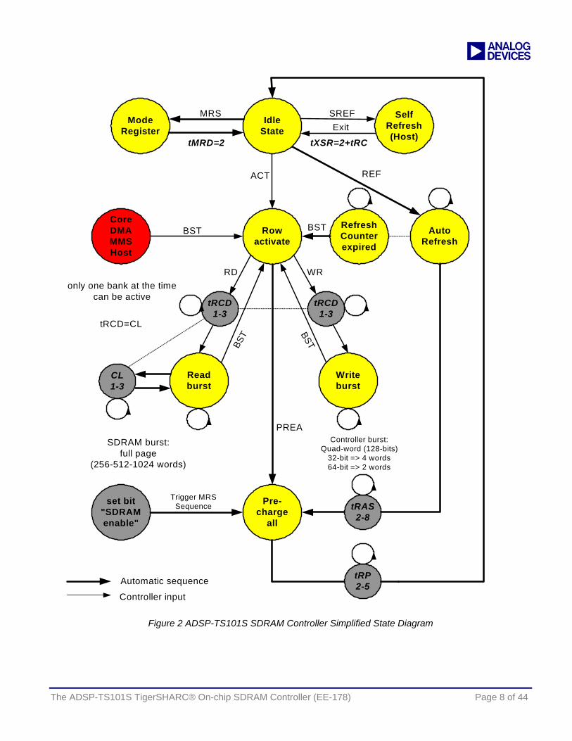
5.4 Simplified State Diagram
The following state diagram (Figure 2) shows all possible SDRAM commands sequences to help analyze the controller’s functionality.
The ADSP-TS101S TigerSHARC® On-chip SDRAM Controller (EE-178) Page 7 of 44
a
Pre-charge
all
Writeburst
Readburst
Rowactivate
IdleState
ModeRegister
SelfRefresh(Host)
AutoRefresh
MRS SREFExit
ACT REF
WR
PREA
Trigger MRSSequence
Automatic sequence
Controller input
tMRD=2 tXSR=2+tRC
BST BST
set bit"SDRAMenable"
BST RefreshCounterexpired
SDRAM burst:full page
(256-512-1024 words)
only one bank at the timecan be active
CoreDMAMMSHost
tRCD1-3
tRCD1-3
tRAS2-8
tRP2-5
RD
CL1-3
BST
tRCD=CL
Controller burst:Quad-word (128-bits)
32-bit => 4 words64-bit => 2 words
Figure 2 ADSP-TS101S SDRAM Controller Simplified State Diagram
The ADSP-TS101S TigerSHARC® On-chip SDRAM Controller (EE-178) Page 8 of 44
a
The ADSP-TS101S TigerSHARC® On-chip SDRAM Controller (EE-178) Page 9 of 44
6 SDRAM Controller Properties Following, the ADSP-TS101S on-chip SDRAM controller properties are examined:
6.1 Address Mapping Scheme
There are various possibilities when accessing the SDRAM. For instance, all rows in a bank can be accessed sequentially, or all banks in a row. PC DIMM modules are accessed in a different manner compared to a typical DSP application. The ADSP-TS101S controller uses a hardware map scheme optimized for digital signal processing.
The address mapping scheme is decoded from the page size and the bus width (both configurable by software in the SDRCON and SYSCON registers respectively; refer to section 7 SDRAM Programming). For more information regarding the address mapping scheme, refer to the SDRAM chapter of the ADSP-TS101 TigerSHARC Processor Hardware Reference [1].
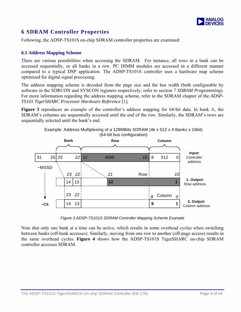
Figure 3 reproduces an example of the controller’s address mapping for 64-bit data. In bank A, the SDRAM’s columns are sequentially accessed until the end of the row. Similarly, the SDRAM’s rows are sequentially selected until the bank’s end.
Column
Row
14 13 12 1
8
9
0
1
Input:Controlleraddress
1. Output:Row address
2. Output:Column address
Example: Address Multiplexing of a 128MBits SDRAM (4k x 512 x 4 Banks x 16bit)(64-bit bus configuration)
4096 5122631
~MSSD
~CS
1021
Row Column
23 22 21 10
23 22
Bank
25 22
14 1308
Figure 3 ADSP-TS101S SDRAM Controller Mapping Scheme Example
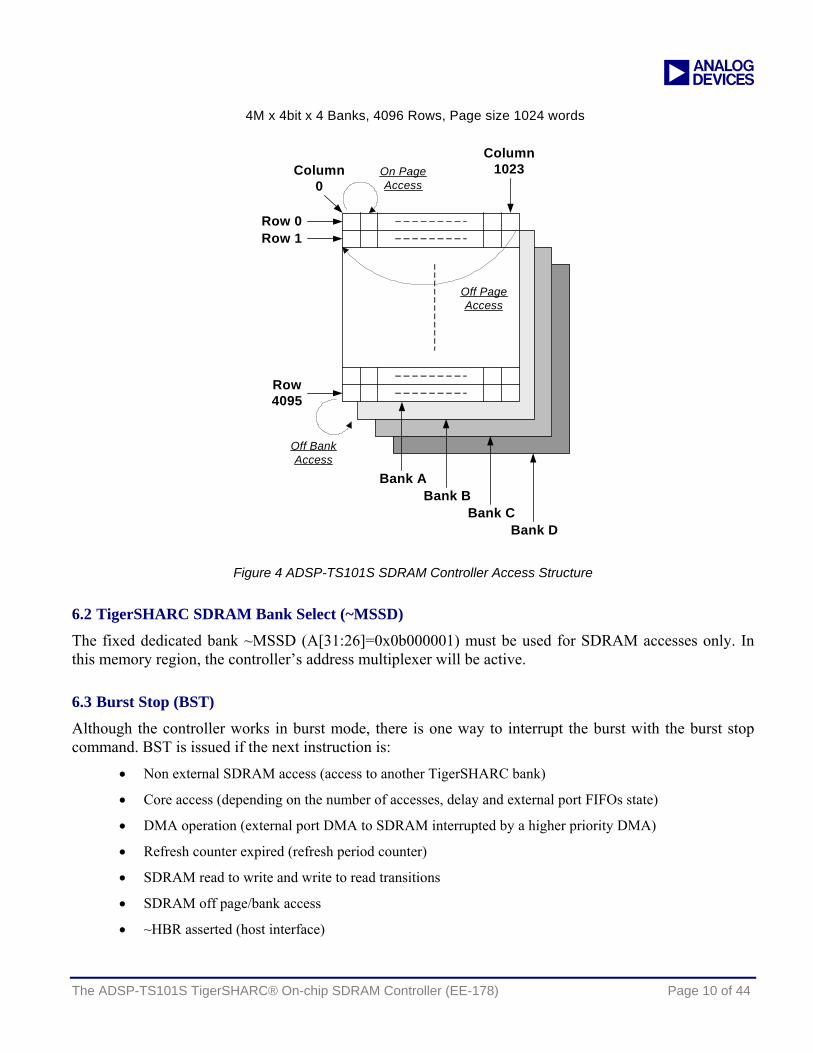
Note that only one bank at a time can be active, which results in some overhead cycles when switching between banks (off-bank accesses). Similarly, moving from one row to another (off-page access) results in the same overhead cycles. Figure 4 shows how the ADSP-TS101S TigerSHARC on-chip SDRAM controller accesses SDRAM.
a
4M x 4bit x 4 Banks, 4096 Rows, Page size 1024 words
Off PageAccess
On PageAccess
Column0
Column1023
Row4095
Row 0Row 1
Bank ABank B
Bank CBank D
Off BankAccess
Figure 4 ADSP-TS101S SDRAM Controller Access Structure
6.2 TigerSHARC SDRAM Bank Select (~MSSD)
The fixed dedicated bank ~MSSD (A[31:26]=0x0b000001) must be used for SDRAM accesses only. In this memory region, the controller’s address multiplexer will be active.
6.3 Burst Stop (BST)
Although the controller works in burst mode, there is one way to interrupt the burst with the burst stop command. BST is issued if the next instruction is:
• Non external SDRAM access (access to another TigerSHARC bank)
• Core access (depending on the number of accesses, delay and external port FIFOs state)
• DMA operation (external port DMA to SDRAM interrupted by a higher priority DMA)
• Refresh counter expired (refresh period counter)
• SDRAM read to write and write to read transitions
• SDRAM off page/bank access
• ~HBR asserted (host interface)
The ADSP-TS101S TigerSHARC® On-chip SDRAM Controller (EE-178) Page 10 of 44
a
The ADSP-TS101S TigerSHARC® On-chip SDRAM Controller (EE-178) Page 11 of 44
• During a Bus Transition Cycle (multiprocessing)
6.4 Data Mask Function ([H:L]DQM)
The [H:L]DQM pins are used by the controller to mask write operations. HDQM masks the SDRAM DQ buffers when performing 32-bit writes to even addresses in a 64-bit bus configuration. LDQM masks the SDRAM DQ buffers when performing writes to odd addresses in a 64-bit bus configuration. This data mask function does not apply for read operations, where the LDQM and HDQM pins are always low (inactive).
This is summarized in the following table:
Bus Width* 64-bit 32-bit
Access type 32-bit Even 32-bit Odd 64-bit 32-bit Even/Odd
HDQM 1 0 0 x
LDQM 0 1 0 0
x = don’t care 0 = logic 0, 1 = logic 1 *Bus Width bit setting in SYSCON
6.5 SDRAM Bank Select
The next tables show the address lines selection for the different banks:
2-banked access
Banks A[11:15] SDA10
Bank_A 0 0
Bank_B 1 0
Banks A/B x 1
x = don’t care, 0 = logic 0, 1 = logic 1 Note: Any address line from address range A[11:15] can be used for bank select as long as they are not driven as a row or column address.
4-banked access
Banks A[11,13,15] A[12,14] SDA10
Bank_A 0 0 0
Bank_B 1 0 0
Bank_C 0 1 0
Bank_D 1 1 0
All Banks X X 1
x = don’t care, 0 = logic 0, 1 = logic 1 Note: Any address line pair from address range A[11:15] can be used for bank select as long as they are not driven as a row- or column address.
a 6.6 Controller Address 10 (SDA10)
This pin provides a special solution to gain control of the SDRAM, even when the DSP operates as a slave (multiprocessing). The SDA10 pin allows access to all banks simultaneously during a refresh and precharge-all command. This pin must be connected to the A10 pin of the SDRAM.
Note that the SDA10 pin replaces the DSP’s A[10] and A[11] pins in a 32-bit and 64-bit bus width configuration, respectively. Also, during access to the ~MSSD space, these pins are inactive.
6.7 Burst Mode
Although the SDRAM device is programmed for full page burst, the controller uses quad-word (128-bits) burst mode. For 32-bit bus width, the burst length is 4 words, and for 64-bit width, the burst length is 2 words. Only the first read or write command is accompanied with an external address, which is driven by the controller until the burst is interrupted by another address.
It’s also important to note that the SDRAM Controller burst mode cannot be changed.
6.8 Precharge All (PREA)
This command precharges all SDRAM banks simultaneously (SDA10 high to select all banks), which brings the banks into idle state.
Although only one bank at a time can be active, the controller does not support a single bank precharge.
6.9 Circular Access
The controller supports circular accesses during sequential read or writes within a page, performing a fixed throughput of 1 cycle/word. At the end of the page (defined in the SDRCON register), the instructions xR3:0=Q[j1+=last_word];; followed by xR7:4=Q[j1+=first_word];; are also executed with a 1 cycle/word throughput.
This functionality is similar to the IALU’s circular buffering mode supported by the TigerSHARC core.
6.10 Auto-Refresh (REF)
After the SDRAM registers the auto-refresh command, it internally asserts CAS and delays RAS to execute a row’s refresh. The row interval is typically tRC=15,625 µs, which is a good compromise between data access time and the refresh reliability. The limit of refresh period is given through the tREFmax spec.
Note that the controller does not support burst refresh.
6.11 Self-Refresh (SREF)
The self-refresh is a very effective way of reducing the application’s power consumption to a minimum. When a host processor gains control of the cluster bus, the TigerSHARC SDRAM controller brings the SDRAM into self-refresh mode before the bus is relinquished to the host. The SDRAM starts refreshing itself triggered by an internal timer. The controller does not allow bringing the SDRAM into self-refresh mode by software, only during host accesses.
The ADSP-TS101S TigerSHARC® On-chip SDRAM Controller (EE-178) Page 12 of 44
a 6.12 Mode Register Set (MRS)
During the MRS command, the SDRAM controller initializes the SDRAM with the following fixed settings:
• Burst length is hardwired to full page burst • Burst type is hardwired to sequential burst • Read Latency (CL) is user specified (1-3 cycles)
The ADSP-TS101S TigerSHARC® On-chip SDRAM Controller (EE-178) Page 13 of 44
a
7 SDRAM Programming Before external bus transactions to SDRAM start, the system and SDRAM control registers must be configured accordingly.
7.1 SYSCON Register
The SYSCON register is the system configuration register and must be configured after hardware reset at the beginning of the source code. This register may only be configured once, and additional write to SYSCON after the first are ignored.
This register is composed of different fields, although only the following applies for SDRAM:
Bus Width: For proper operation, ensure that the dedicated bus width bits settings is:
• 0: 32-bit bus
• 1: 64-bit bus
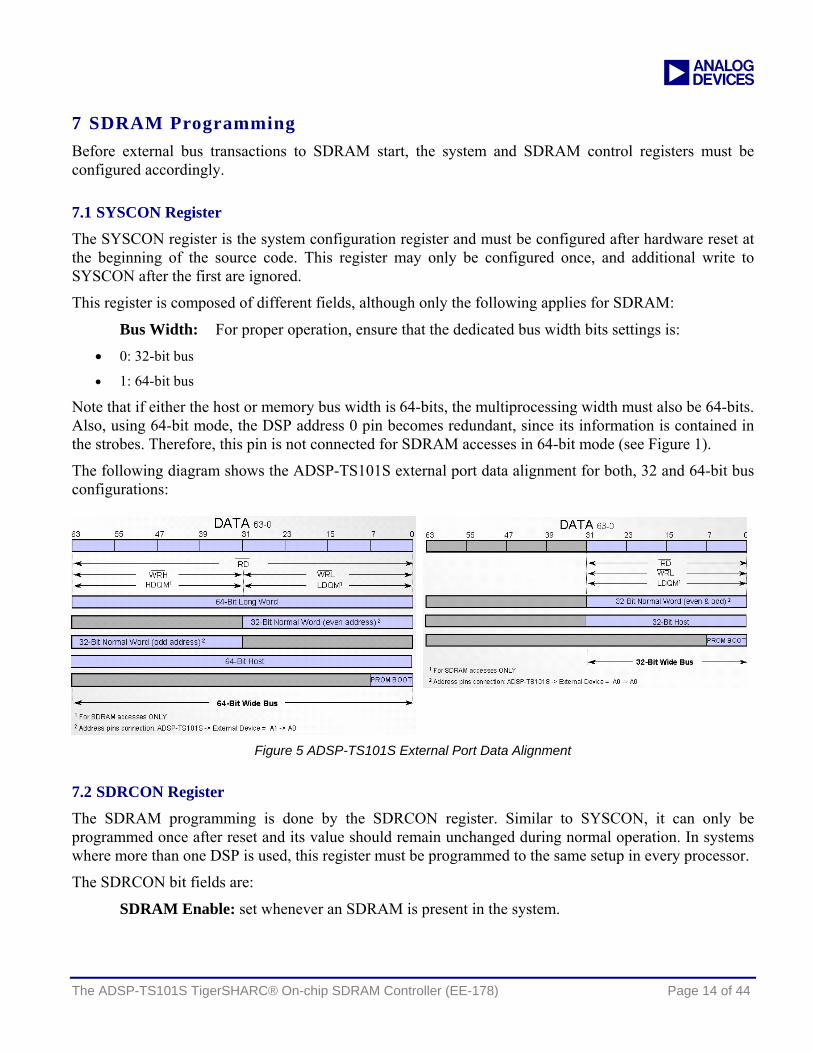
Note that if either the host or memory bus width is 64-bits, the multiprocessing width must also be 64-bits. Also, using 64-bit mode, the DSP address 0 pin becomes redundant, since its information is contained in the strobes. Therefore, this pin is not connected for SDRAM accesses in 64-bit mode (see Figure 1).
The following diagram shows the ADSP-TS101S external port data alignment for both, 32 and 64-bit bus configurations:
Figure 5 ADSP-TS101S External Port Data Alignment
7.2 SDRCON Register
The SDRAM programming is done by the SDRCON register. Similar to SYSCON, it can only be programmed once after reset and its value should remain unchanged during normal operation. In systems where more than one DSP is used, this register must be programmed to the same setup in every processor.
The SDRCON bit fields are:
SDRAM Enable: set whenever an SDRAM is present in the system.
The ADSP-TS101S TigerSHARC® On-chip SDRAM Controller (EE-178) Page 14 of 44

a CAS Latency: this bit is used to define the read latency (CLmin) related to the vendor’s device. This value can be set from 1 to 3 cycles, depending on the SDRAM characteristics and the clock frequency.
Pipe depth: this bit allows the SDRAM address and control lines to be pipelined. Setting this bit introduces a one-cycle delay during read and write accesses.
Page Boundary: this bit determines the page size of the SDRAM, which can be set to 256, 512, or 1024 words.
Refresh Counters: these bits enable coordination of the clock rate with the SDRAM’s required refresh rate. It is used to select between 4 different refresh rates calculated with the following equation:
( )raterefreshClockRowstREFClockCycles _⋅=⎟
⎠⎞
⎜⎝⎛ ⋅=
The ADSP-TS101S supports refresh rates of 600, 900, 1200 or 2400 cycles. The following table illustrates how to select between the different rates based on the formula above.
Clock frequency (MHz) Refresh rate (cycles) SDRCON Bits [8:7]
f <60 600 00
60≤ f <80 900 01
80≤ f <150* 1200 10
f ≥150* 2400 11
* Note that the maximum external port frequency supported by the ADSP-TS101S is 100 MHz.
Precharge to RAS delay (tRP): this bit defines the precharge time (tRPmin) related to the vendor’s device. This value can be set from 2 to 5 cycles. Note that this parameter is defined in most SDRAMs in nanoseconds delay rather than number of cycles.
RAS to precharge delay (tRAS): this bit is used to define the row active time (tRASmin) related to the vendor’s device. This value can be programmed from 2 to 8 cycles. Note that this parameter is also defined in nanoseconds rather than number of cycles.
Initialization Sequence: this bit determines the order of the MRS (Mode Register set) and refresh sequences. When set, MRS follows refresh in the SDRAM initialization sequence. Otherwise, the MRS precedes refresh:
Init Sequence = 0 • PREA command - brings the SDRAM in the defined idle state.
• 8 REF commands - charges SDRAM’s internal nodes.
• MRS command - initializes the SDRAM’s working mode.
Init Sequence = 1 • PREA command - brings the SDRAM in the defined idle state.
• MRS command - initializes the SDRAM’s working mode.
The ADSP-TS101S TigerSHARC® On-chip SDRAM Controller (EE-178) Page 15 of 44
a • 8 REF commands - charges SDRAM’s internal nodes.
tRAS and tRP are used for the refresh cycle, which can be expressed as: tRFC=tRAS+tRP. Also, the specification requires that tRASmin, tRPmin, and CLmin are defined as a integer fraction of the SCLK period.
7.3 SDRAM Mode of Operation
During the MRS, address bits ADDR[13:0] of the SDRAM are used to program the device. The MRS is executed during power-up only and it is always issued by the TigerSHARC with ID=000. MRS initializes the following parameters:
• A[2:0] - Burst length is hardwired to full page burst. • A[3] - Burst type is hardwired to sequential burst. • A[6:4] - Latency mode set according to the CAS latency programmed in SDRCON (1-3 cycles). • A[13:7]- hardwired to zero (reserved mode of operation for future needs).
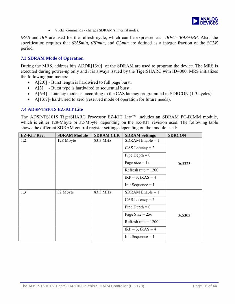
7.4 ADSP-TS101S EZ-KIT Lite
The ADSP-TS101S TigerSHARC Processor EZ-KIT Lite™ includes an SDRAM PC-DIMM module, which is either 128-Mbyte or 32-Mbyte, depending on the EZ-KIT revision used. The following table shows the different SDRAM control register settings depending on the module used:
EZ-KIT Rev. SDRAM Module SDRAM CLK SDRAM Settings SDRCON SDRAM Enable = 1
CAS Latency = 2
Pipe Depth = 0
Page size = 1k
Refresh rate = 1200
tRP = 3, tRAS = 4
1.2 128 Mbyte 83.3 MHz
Init Sequence = 1
0x5323
SDRAM Enable = 1
CAS Latency = 2
Pipe Depth = 0
Page Size = 256
Refresh rate = 1200
tRP = 3, tRAS = 4
1.3 32 Mbyte 83.3 MHz
Init Sequence = 1
0x5303
The ADSP-TS101S TigerSHARC® On-chip SDRAM Controller (EE-178) Page 16 of 44
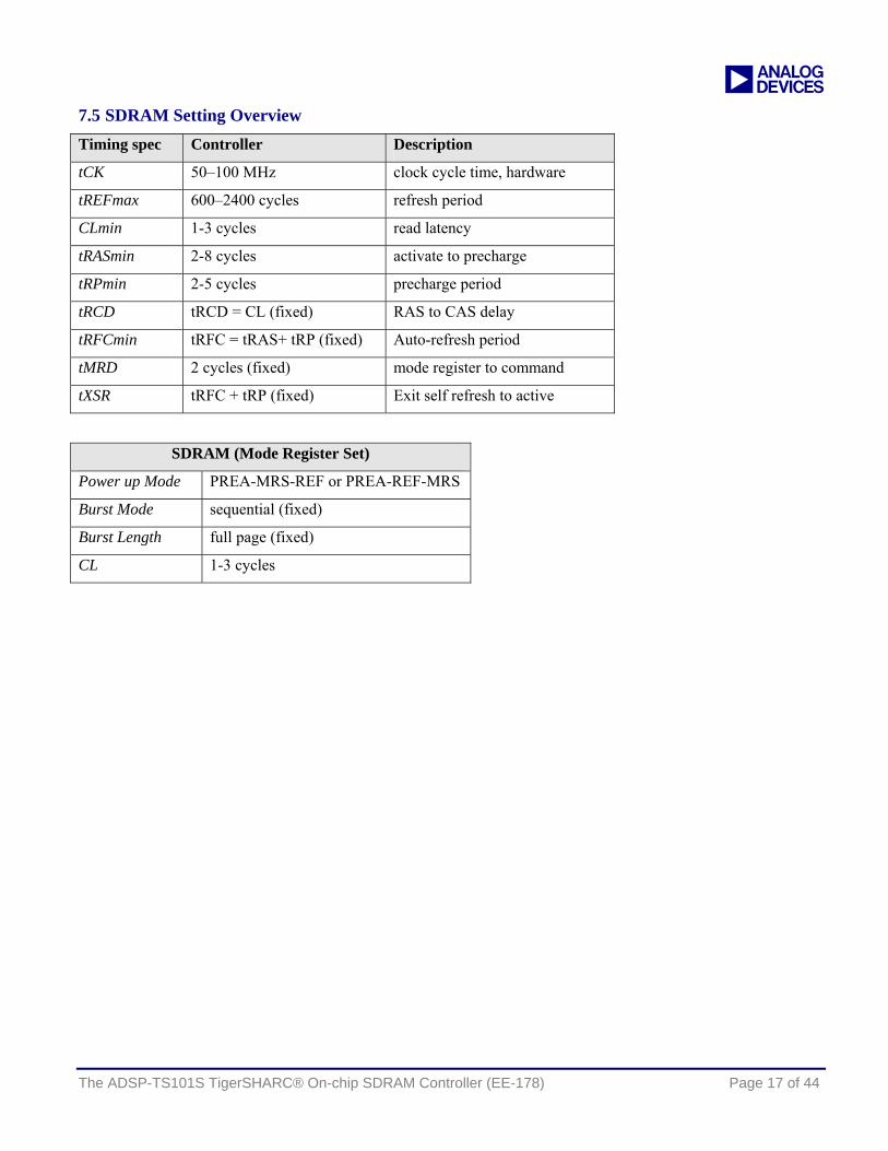
a 7.5 SDRAM Setting Overview Timing spec Controller Description
tCK 50–100 MHz clock cycle time, hardware
tREFmax 600–2400 cycles refresh period
CLmin 1-3 cycles read latency
tRASmin 2-8 cycles activate to precharge
tRPmin 2-5 cycles precharge period
tRCD tRCD = CL (fixed) RAS to CAS delay
tRFCmin tRFC = tRAS+ tRP (fixed) Auto-refresh period
tMRD 2 cycles (fixed) mode register to command
tXSR tRFC + tRP (fixed) Exit self refresh to active
SDRAM (Mode Register Set)
Power up Mode PREA-MRS-REF or PREA-REF-MRS
Burst Mode sequential (fixed)
Burst Length full page (fixed)
CL 1-3 cycles
The ADSP-TS101S TigerSHARC® On-chip SDRAM Controller (EE-178) Page 17 of 44
a
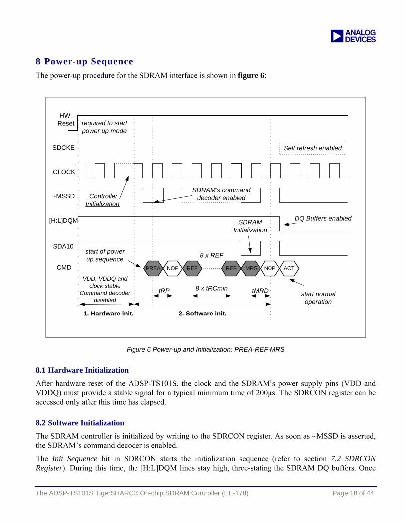
8 Power-up Sequence The power-up procedure for the SDRAM interface is shown in figure 6:
HW-Reset
CMD REF
[H:L]DQM
REFPREA NOP MRS NOP ACT
VDD, VDDQ andclock stable
Command decoderdisabled
CLOCK
~MSSD
1. Hardware init.
ControllerInitialization
SDRAM's commanddecoder enabled
DQ Buffers enabled
start of powerup sequence
SDRAMInitialization
8 x tRCmin
SDA10
tRP tMRD
SDCKE Self refresh enabled
required to startpower up mode
8 x REF
start normaloperation
2. Software init.
Figure 6 Power-up and Initialization: PREA-REF-MRS
8.1 Hardware Initialization
After hardware reset of the ADSP-TS101S, the clock and the SDRAM’s power supply pins (VDD and VDDQ) must provide a stable signal for a typical minimum time of 200µs. The SDRCON register can be accessed only after this time has elapsed.
8.2 Software Initialization
The SDRAM controller is initialized by writing to the SDRCON register. As soon as ~MSSD is asserted, the SDRAM’s command decoder is enabled.
The Init Sequence bit in SDRCON starts the initialization sequence (refer to section 7.2 SDRCON Register). During this time, the [H:L]DQM lines stay high, three-stating the SDRAM DQ buffers. Once
The ADSP-TS101S TigerSHARC® On-chip SDRAM Controller (EE-178) Page 18 of 44
a the initialization sequence is completed, the buffers are enabled and the SDRAM is ready for normal operation.
The time elapsed before the first access to SDRAM can be represented as:
taccess ≈ tRP + 8(tRAS + tRP) + tMRD (SCLK cycles)
Note that in order to properly initialize the SDRAM, the first access is delayed with the internal acknowledge until the power up sequence has finished.
8.3 SDRAM Initialization Example
This section shows how to initialize the SDRCON register according to the following device specifications.
• 2M x 32 bit SDRAM: • 4 banks, page size: 256 words • SDRAM Clock: 60 MHz • Speed grade: 70 • Refresh cycles: 4096/64ms • Power-up mode: PRE - MRS - REF • CLmin=2 @60MHz, tRASmin=42 ns, tRPmin=20 ns • No self refresh • No buffering
Therefore, the SDRAM initialization code would look as follows: j1 = j31 + 0x00004883;; // ENA=1, CL=2, pipedepth=0, page=256w
SDRCON = j1;; // refresh rate=900, trp=2, tras=3, init=1
Note that the minimum timing specifications for tRAS, tRP, and CL must be guaranteed. Setting these values larger than the minimum required causes a loss of performance. (e.g. longer delay cycles or unnecessary refresh cycles).
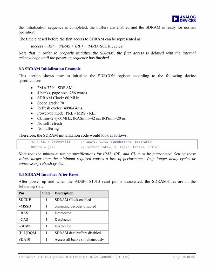
8.4 SDRAM Interface After Reset
After power up and when the ADSP-TS101S reset pin is deasserted, the SDRAM-lines are in the following state: Pin State Description
SDCKE 1 SDRAM Clock enabled
~MSSD 1 command decoder disabled
~RAS 1 Deselected
~CAS 1 Deselected
~SDWE 1 Deselected
[H:L]DQM 1 SDRAM data buffers disabled
SDA10 1 Access all banks simultaneously
The ADSP-TS101S TigerSHARC® On-chip SDRAM Controller (EE-178) Page 19 of 44
a
9 DMA Transfers Direct Memory Access (DMA) is a mechanism for transferring data without core involvement. Transfers can be between internal and external memory, or between external memory and an external peripheral.
9.1 Internal Memory and SDRAM
The TigerSHARC DMA controller can be used to transfer data from the DSP’s internal memory to external SDRAM. Similarly, the SDRAM can be used as the source and the internal memory as the destination.
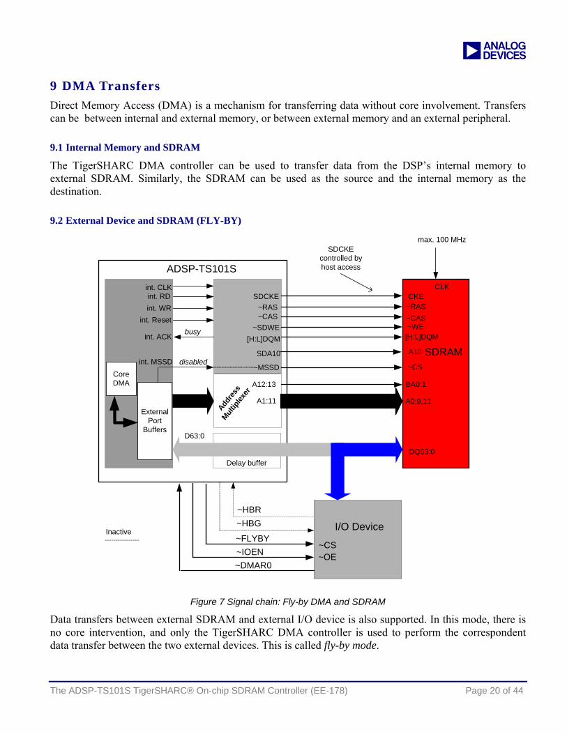
9.2 External Device and SDRAM (FLY-BY)
CLKCKE
~RAS~CAS~WE
[H:L]DQM
~CS
SDCKE~RAS~CAS
~SDWE[H:L]DQM
SDA10
DQ63:0
BA0:1
int. CLKint. RDint. WR
int. Reset
int. ACK
D63:0
SDRAM
ADSP-TS101S
A0:9,11
~MSSD
max. 100 MHz
A10
Delay buffer
disabled
busy
SDCKEcontrolled byhost access
A12:13
I/O Device
~HBR~HBG
int. MSSD
~FLYBY~IOEN~DMAR0
A1:11
Addre
ssMult
iplex
er
Inactive
CoreDMA
ExternalPort
Buffers
~OE~CS
Figure 7 Signal chain: Fly-by DMA and SDRAM
Data transfers between external SDRAM and external I/O device is also supported. In this mode, there is no core intervention, and only the TigerSHARC DMA controller is used to perform the correspondent data transfer between the two external devices. This is called fly-by mode.
The ADSP-TS101S TigerSHARC® On-chip SDRAM Controller (EE-178) Page 20 of 44
a When the I/O-device wants to transfer data, it asserts the ~DMAR0 pin – only DMA channel 0 can be used for fly-by transactions. Note that the ~DMAR0 is edge sensitive. Each assertion (falling edge) of the ~DMAR0 signal represents one transaction. The ~FLBY is used as a chip select for the I/O device and ~IOEN allows read transaction (output enable) from the I/O.
For more details on the TigerSHARC DMA controller and Fly-by Mode, refer to the “Direct Memory Access” and the “Cluster Bus” chapters of the ADSPTS101 TigerSHARC Processor Hardware Reference Manual [1]. Also, “Understanding DMA on the ADSP-TS101S (EE-143)” [4] is available.
The ADSP-TS101S TigerSHARC® On-chip SDRAM Controller (EE-178) Page 21 of 44

a
10 SDRAM Interface in Host Mode Figure 8 shows a possible signal chain between the ADSP-TS101S, SDRAM, and a host processor.
CLKCKE
~RAS~CAS~WE
[H:L]DQM
~CS
SDCKE~RAS~CAS
~SDWE[H:L]DQM
SDA10
DQ63:0
BA0:1
int. CLKint. RDint. WR
int. Reset
int. ACK
D63:0
SDRAM
ADSP-TS101S
A0:9, 11
~MSSD
max. 100 MHz
A10
Delay buffer
disabled
busy
SDCKEcontrolled byhost access
A12:13
Host
int. MSSD
A31:0
Inactive
CoreDMA
ExternalPort
Buffers
I/O Device
~HBR~HBG
~FLYBY~IOEN~DMAR0
~OE~CS
Figure 8 Signal Chain: Host to ADSP-TS101S
Host accesses are initiated by having the host assert ~HBR to request the external bus to the TigerSHARC. Thereafter, the TigerSHARC responds to this request by asserting ~HBG, granting the bus to the host. The host becomes bus master and can now access the internal TigerSHARC resources through its multiprocessor memory space.
Note that during ~HBG low, the SDRAM is in self-refresh mode. This limits the host device to not being able to access the SDRAM using the TigerSHARC’s SDRAM controller (fly-by mode). Thus, during host transactions, the SDRAM can only be accessed by a host using its own SDRAM controller.
The ADSP-TS101S TigerSHARC® On-chip SDRAM Controller (EE-178) Page 22 of 44
a However, a workaround for this may be possible if the host follows the given sequence:
1. Initially, the TigerSHARC is current bus master. To gain control of the bus, the host asserts ~HBR and waits for the TigerSHARC to grant the bus (~HBG)
2. The host becomes bus master and is now able to access the internal resources of the TigerSHARC. 3. The host sets up a DMA transfer to have the TigerSHARC transfer data to SDRAM upon host
requests (DMA request line ~DMAR0). 4. The host relinquishes the bus (de-asserts ~HBR), which brings the SDRAM out of self-refresh
mode 5. Finally, the host starts toggling ~DMAR0, indicating to the TigerSHARC to start transmitting data
to the SDRAM.
The ADSP-TS101S TigerSHARC® On-chip SDRAM Controller (EE-178) Page 23 of 44
a
11 Multiprocessing This section covers the arbitration logic used to guarantee multiprocessing systems.
11.1 Command Decoding
The ADSP-TS101S can be connected to a multiprocessor cluster of eight DSPs. Only one TigerSHARC can drive the bus at the time. To build a glueless hardware, the interface works in slave mode as well to detect commands. These commands are MRS, REF, and SREF. Following pins are necessary for detection:
Pin Type Description
SDCKE I/O/T SDRAM Clock Enable
~MSSD I/O/T Memory Select SDRAM (command input)
~RAS I/O/T Row Address Select (command input)
~CAS I/O/T Column Address Select (command input)
~SDWE I/O/T SDRAM Write Enable (command input) I=input, O=output, T=three-state
11.2 MRS Decoding
In TigerSHARC multiprocessor systems where SDRAM is used, the Mode Register Set sequence is only issued by the DSP with ID=000. Therefore, a DSP with ID=000 must be present in every multiprocessor system. The MRS sequence is only issued once before accessing the SDRAM for the first time. It is also important to note that the set-up value initialized in the SDRCON register must be identical for all DSPs in the cluster.
11.3 REF Decoding
This detection helps to synchronize all eight refresh counters. The slave’s refresh counter will be decremented each time the interface detects a refresh. This feature guarantees a periodic refresh and, similarly to the MRS sequence, it requires the exact same settings of SDRCON registers.
11.4 SREF Decoding
This detection helps to synchronize the self-refresh base. When a host requests the bus, the system master brings the SDRAM into self-refresh mode. The slave DSPs recognize the SREF freezing the refresh counters until the self-refresh mode is exited.
11.5 Bus Transition Cycle
The bus transition or turn-over cycle is issued when bus mastership changes between the different TigerSHARCs sharing the cluster bus. This also implies a mastership transition between the SDRAM controllers. Since the new bus master is not able to determine which row in the SDRAM is currently open, the current bus master automatically issues a precharge-all command (PREA) before the bus is
The ADSP-TS101S TigerSHARC® On-chip SDRAM Controller (EE-178) Page 24 of 44
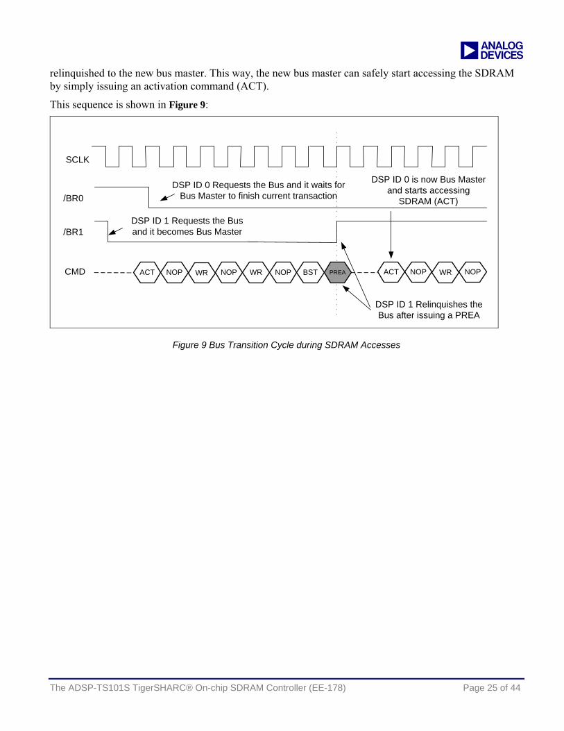
a relinquished to the new bus master. This way, the new bus master can safely start accessing the SDRAM by simply issuing an activation command (ACT).
This sequence is shown in Figure 9:
CMD WR NOP BST
SCLK
/BR0
/BR1
ACT NOP WRNOP PREA WRACT NOP NOP
DSP ID 1 Requests the Busand it becomes Bus Master
DSP ID 0 Requests the Bus and it waits forBus Master to finish current transaction
DSP ID 1 Relinquishes theBus after issuing a PREA
DSP ID 0 is now Bus Masterand starts accessing
SDRAM (ACT)
Figure 9 Bus Transition Cycle during SDRAM Accesses
The ADSP-TS101S TigerSHARC® On-chip SDRAM Controller (EE-178) Page 25 of 44
a
12 SDRAM and Booting
12.1 Loader Kernel
Data must be loaded in SDRAM before runtime. This requires an initialized SDRAM before downloading the data during the boot scenario. The VisualDSP++® loader utility provides this capability.
Three standard loader executables are available for booting either an EPROM (via link ports) or a host processor. Note that independently from the selected boot mode, the SDRAM control register (SDRCON) must be initialized before the user’s application starts writing data to it. This must be done during the first 256-loader kernel words; otherwise the data placed in the SDRAM will get corrupted.
The steps are:
1. ~RESET must be deasserted, ~BMS is sampled 2. Kernel (256 x 32 bit) is transmitted via DMA into the DSP (0x00-0xFF) (~BMS or ~HBG
continuously asserted) 3. Interrupt generation starts kernel execution, SDRAM and controller is initialized (~MSSD asserted for
SDRAM setup) 4. User’s data is loaded into the DSP/SDRAM (~BMS, ~HBG and ~MSSD are toggling requesting the
bus) 5. Kernel is now overwritten with user’s code (~BMS or ~HBG continuously asserted) 6. DSP starts code execution at start address 0x00000000
12.2 Booting Modes
The boot mode is selected at the end of reset by sampling the ~BMS pin. At this stage, four options for beginning operation can be selected:
Mode ~BMS DMA channel
EPROM 0 (Default) Hardwired DMA Channel 0
Link Port 1 Link Port DMA Channels 8-11
Host 1 AutoDMA Channels 0-1
No boot 1 -
If ~BMS is sampled low during reset, EPROM boot is selected. However, if ~BMS is sampled high during reset, the DSP will go into an IDLE state, waiting for host or link boot. Refer to “ADSP-TS101S TigerSHARC Processor Boot Loader Kernels Operation (EE-174)” [5], which describes each mode of operation in more detail.
The ADSP-TS101S TigerSHARC® On-chip SDRAM Controller (EE-178) Page 26 of 44
a
13 SDRAM Interface Throughput This section investigates the SDRAM controller’s performance during data transfers, where the SDRAM is used as either a source or destination. The following settings will be used:
• Silicon = ADSP-TS101S Rev0.0 • SCLK = 60 MHz (external port and SDRAM clock) • LCLK = 180 MHz (core clock) • SYSCON = 0x3A79E7, for 64-bit bus configuration • SDRCON = 0x4883, where Page Boundary = 256 words,
Refresh rate = 900 cycles, tRAS=3 cycles,
tRP=2 cycle, CL=2 cycles,
The following diagrams correspond to the different types of core/IOP accesses to SDRAM. Additionally, a listing of the instructions and SDRAM commands executed during each memory access are listed.
Note that the external bus is configured to 64-bits wide. Therefore, every data word read/written from/to the SDRAM will be 64-bits (i.e. DA1, DA2, DB1, etc.).
The ADSP-TS101S TigerSHARC® On-chip SDRAM Controller (EE-178) Page 27 of 44

a
13.1 Sequential Reads without Interruption
As shown below, uninterrupted sequential reads have a throughput of 1 word per cycle after the first word is read.
SCLK
4 Quad-word Sequential Uninterrupted on Page Reads
ADDR
CMD ACT RDNOP NOP
Row Col
DATA DA1
SDA10
tRCD CL
RD NOP RD NOP RD NOP
DA2 DB1 DB2 DC1 DC2 DD1 DD2
Col Col Col
Burst
Nr. Cycles Core Controller Data 1 xr3:0=q[j1+=j4];; ACT 2 int. ACK NOP 3 int. ACK RD 4 int. ACK NOP 5 xr7:4=q[j1+=j4];; RD DA1 6 int. ACK NOP DA2 7 xr11:8=q[j1+=j4];; RD DB1 8 int. ACK NOP DB2 9 xr15:12=q[j1+=j4];; RD DC1 10 int. ACK NOP DC2 11 int. ACK … DD1 12 int. ACK … DD2
The ADSP-TS101S TigerSHARC® On-chip SDRAM Controller (EE-178) Page 28 of 44
a
13.2 Non Sequential Reads without Interruption
Similar to uninterrupted sequential reads, non-sequential reads also give a 1 word/cycle throughput.
SCLK
4 Quad-word Non-sequential Uninterrupted on Page Reads
ADDR
CMD ACT RDNOP NOP
Row Col
DATA DA1
tRCD CL
RD NOP RD NOP RD NOP
DA2 DB1 DB2 DC1 DC2 DD1 DD2
Col Col Col
Burst
SDA10
Nr. Cycles Core Controller Data 1 xr3:0=q[j1+=j4];; ACT 2 int. ACK NOP 3 int. ACK RD 4 int. ACK NOP 5 xr7:4=q[j1+=j4];; RD DA1 6 int. ACK NOP DA2 7 xr11:8=q[j1+=j4];; RD DB1 8 int. ACK NOP DB2 9 xr15:12=q[j1+=j4];; RD DC1 10 int. ACK NOP DC2 11 int. ACK … DD1 12 int. ACK … DD2
The ADSP-TS101S TigerSHARC® On-chip SDRAM Controller (EE-178) Page 29 of 44
a
13.3 Sequential Reads with minimum Interruption
In this case, an additional core access is performed during a core read from SDRAM, interrupting the data transfer. Similarly, an IOP read is interrupted by a higher priority request to IOP. In this case, the throughput is 1 word every 8 cycles.
SCLK
3 Quad-word Sequential Interrupted on Page Reads
ADDR
CMD ACT RDNOP NOP
Row Col
DATA DA1
SDA10
tRCD CL
RD NOP RD NOP
DA2 DB1 DB2 DC1
Col Col
Burst
BST NOP
6 NOPs Burst
CL
NOP
Nr. Cycles Core Controller Data 1 xr3:0=q[j1+=j4];; ACT 2 int. ACK NOP 3 int. ACK RD 4 int. ACK NOP 5 xr0=r1+r2;; BST DA1 6 int. ACK NOP DA2 7 int. ACK NOP 8 int. ACK NOP 9 int. ACK NOP 10 int. ACK NOP 11 int. ACK NOP 12 xr7:4=q[j1+=j4];; RD 13 int. ACK NOP 14 xr15:12=q[j1+=j4];; RD DB1 15 int. ACK NOP DB2 16 int. ACK NOP DC1 17 int. ACK NOP DC2
The ADSP-TS101S TigerSHARC® On-chip SDRAM Controller (EE-178) Page 30 of 44
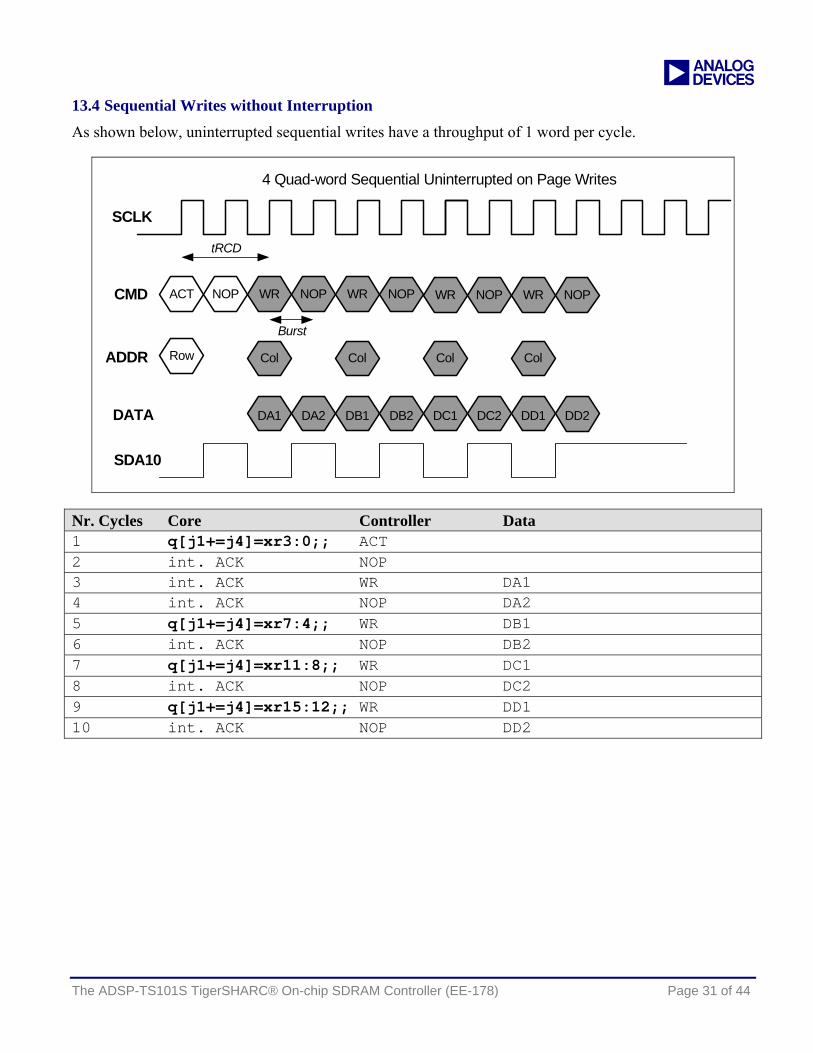
a 13.4 Sequential Writes without Interruption
As shown below, uninterrupted sequential writes have a throughput of 1 word per cycle.
SCLK
4 Quad-word Sequential Uninterrupted on Page Writes
ADDR
CMD ACT WRNOP NOP WR
Row
DATA
NOP
tRCD
WR NOP WR NOP
Col Col ColCol
DB2DB1DA2DA1 DD2DD1DC2DC1
Burst
SDA10
Nr. Cycles Core Controller Data 1 q[j1+=j4]=xr3:0;; ACT 2 int. ACK NOP 3 int. ACK WR DA1 4 int. ACK NOP DA2 5 q[j1+=j4]=xr7:4;; WR DB1 6 int. ACK NOP DB2 7 q[j1+=j4]=xr11:8;; WR DC1 8 int. ACK NOP DC2 9 q[j1+=j4]=xr15:12;; WR DD1 10 int. ACK NOP DD2
The ADSP-TS101S TigerSHARC® On-chip SDRAM Controller (EE-178) Page 31 of 44
a
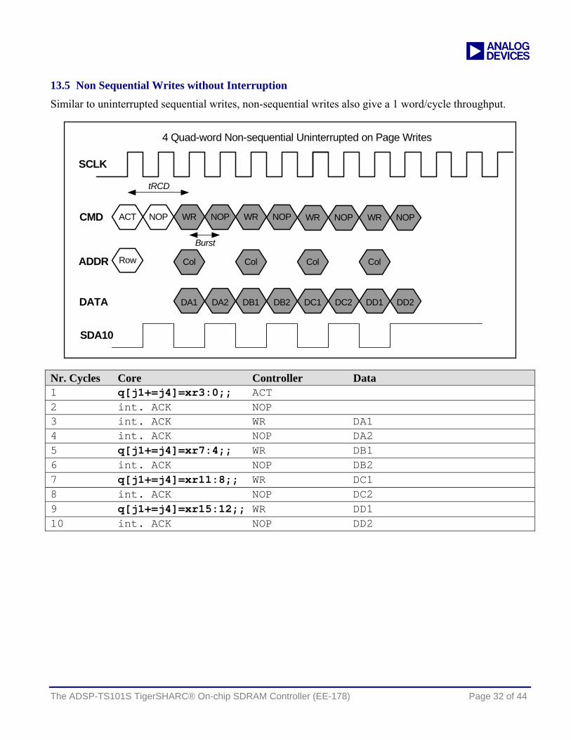
13.5 Non Sequential Writes without Interruption
Similar to uninterrupted sequential writes, non-sequential writes also give a 1 word/cycle throughput.
SCLK
4 Quad-word Non-sequential Uninterrupted on Page Writes
ADDR
CMD ACT WRNOP NOP WR
Row
DATA
NOP
tRCD
WR NOP WR NOP
Col Col ColCol
DB2DB1DA2DA1 DD2DD1DC2DC1
Burst
SDA10
Nr. Cycles Core Controller Data 1 q[j1+=j4]=xr3:0;; ACT 2 int. ACK NOP 3 int. ACK WR DA1 4 int. ACK NOP DA2 5 q[j1+=j4]=xr7:4;; WR DB1 6 int. ACK NOP DB2 7 q[j1+=j4]=xr11:8;; WR DC1 8 int. ACK NOP DC2 9 q[j1+=j4]=xr15:12;; WR DD1 10 int. ACK NOP DD2
The ADSP-TS101S TigerSHARC® On-chip SDRAM Controller (EE-178) Page 32 of 44
a
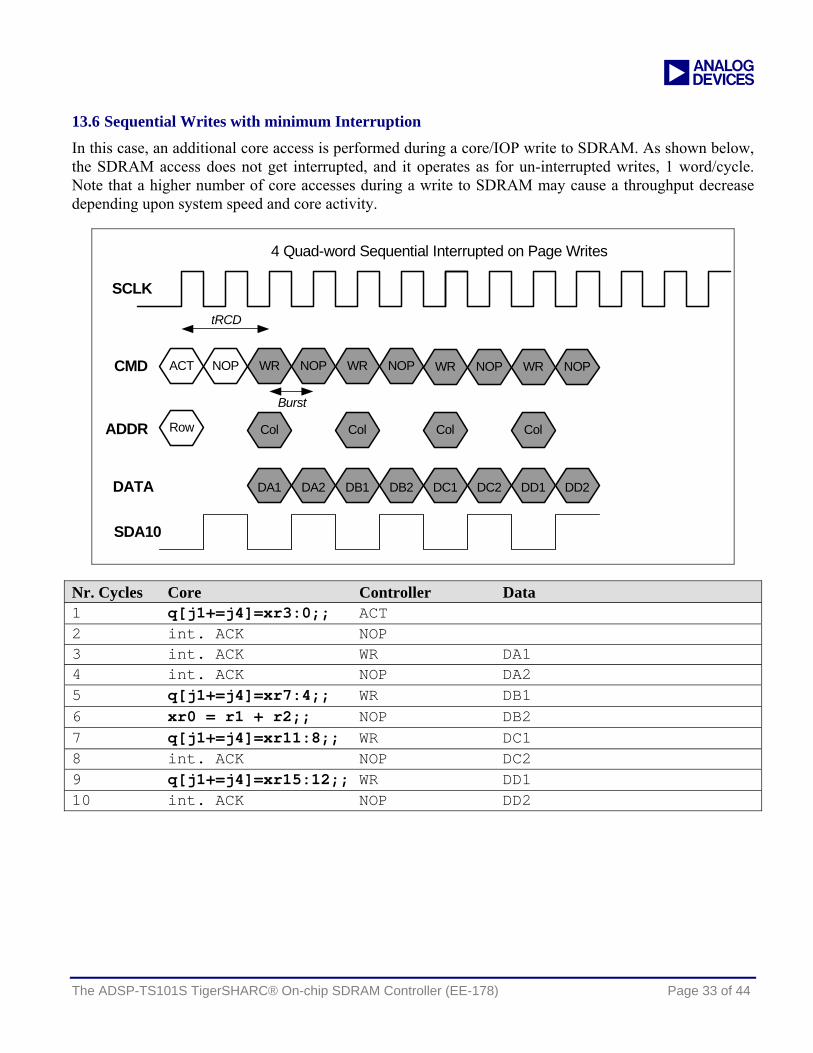
13.6 Sequential Writes with minimum Interruption
In this case, an additional core access is performed during a core/IOP write to SDRAM. As shown below, the SDRAM access does not get interrupted, and it operates as for un-interrupted writes, 1 word/cycle. Note that a higher number of core accesses during a write to SDRAM may cause a throughput decrease depending upon system speed and core activity.
SCLK
4 Quad-word Sequential Interrupted on Page Writes
ADDR
CMD ACT WRNOP NOP WR
Row
DATA
NOP
tRCD
WR NOP WR NOP
Col Col ColCol
DB2DB1DA2DA1 DD2DD1DC2DC1
Burst
SDA10
Nr. Cycles Core Controller Data 1 q[j1+=j4]=xr3:0;; ACT 2 int. ACK NOP 3 int. ACK WR DA1 4 int. ACK NOP DA2 5 q[j1+=j4]=xr7:4;; WR DB1 6 xr0 = r1 + r2;; NOP DB2 7 q[j1+=j4]=xr11:8;; WR DC1 8 int. ACK NOP DC2 9 q[j1+=j4]=xr15:12;; WR DD1 10 int. ACK NOP DD2
The ADSP-TS101S TigerSHARC® On-chip SDRAM Controller (EE-178) Page 33 of 44
a
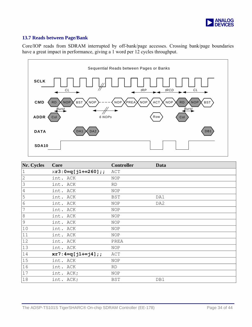
13.7 Reads between Page/Bank
Core/IOP reads from SDRAM interrupted by off-bank/page accesses. Crossing bank/page boundaries have a great impact in performance, giving a 1 word per 12 cycles throughput.
SCLK
Sequential Reads between Pages or Banks
ADDR
CMD RD NOPPREA ACT NOPNOP
DATA DA1
RDNOP
Row
NOP NOP
DB1
Col Col
CL tRP tRCD
BST
DA2
BST
6 NOPs
CL
SDA10
Burst Burst
Nr. Cycles Core Controller Data 1 xr3:0=q[j1+=260];; ACT 2 int. ACK NOP 3 int. ACK RD 4 int. ACK NOP 5 int. ACK BST DA1 6 int. ACK NOP DA2 7 int. ACK NOP 8 int. ACK NOP 9 int. ACK NOP 10 int. ACK NOP 11 int. ACK NOP 12 int. ACK PREA 13 int. ACK NOP 14 xr7:4=q[j1+=j4];; ACT 15 int. ACK NOP 16 int. ACK RD 17 int. ACK; NOP 18 int. ACK; BST DB1
The ADSP-TS101S TigerSHARC® On-chip SDRAM Controller (EE-178) Page 34 of 44

a 13.8 Writes between Page/Bank
Core/IOP writes to SDRAM interrupted by off-bank/page accesses. Like for read accesses, although smaller, crossing bank/page boundaries have a great impact in performance, giving a 1 word per 6 cycles throughput.
SCLK
Sequential Writes between Pages or Banks
ADDR
CMD WR NOPPREA ACT NOP
DATA DA1
WR
Row
NOP NOP
DB1
Col Col
tRP tRCD
BST
DA2
SDA10
Burst Burst
DB2
Nr. Cycles Core Controller Data 1 q[j1+=260]=xr3:0;; ACT 2 int. ACK NOP 3 int. ACK WR DA1 4 int. ACK NOP DA2 5 int. ACK BST 6 int. ACK PREA 7 int. ACK NOP 8 q[j1+=j4]=xr7:4;; ACT 9 int. ACK NOP 10 int. ACK WR DB1 11 int. ACK NOP DB2
The ADSP-TS101S TigerSHARC® On-chip SDRAM Controller (EE-178) Page 35 of 44
a
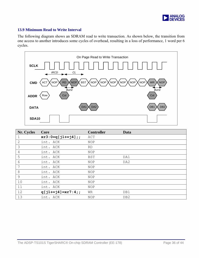
13.9 Minimum Read to Write Interval
The following diagram shows an SDRAM read to write transaction. As shown below, the transition from one access to another introduces some cycles of overhead, resulting in a loss of performance, 1 word per 6 cycles.
SCLK
On Page Read to Write Transaction
ADDR
NOP NOPCMD ACT NOPRDNOP NOP NOP WR
Row Col Col
DATA DA1 DB2
NOP NOP NOP
CLtRCD
Burst
DA2
Burst
DB1
BST
SDA10
Nr. Cycles Core Controller Data 1 xr3:0=q[j1+=j4];; ACT 2 int. ACK NOP 3 int. ACK RD 4 int. ACK NOP 5 int. ACK BST DA1 6 int. ACK NOP DA2 7 int. ACK NOP 8 int. ACK NOP 9 int. ACK NOP 10 int. ACK NOP 11 int. ACK NOP 12 q[j1+=j4]=xr7:4;; WR DB1 13 int. ACK NOP DB2
The ADSP-TS101S TigerSHARC® On-chip SDRAM Controller (EE-178) Page 36 of 44
a
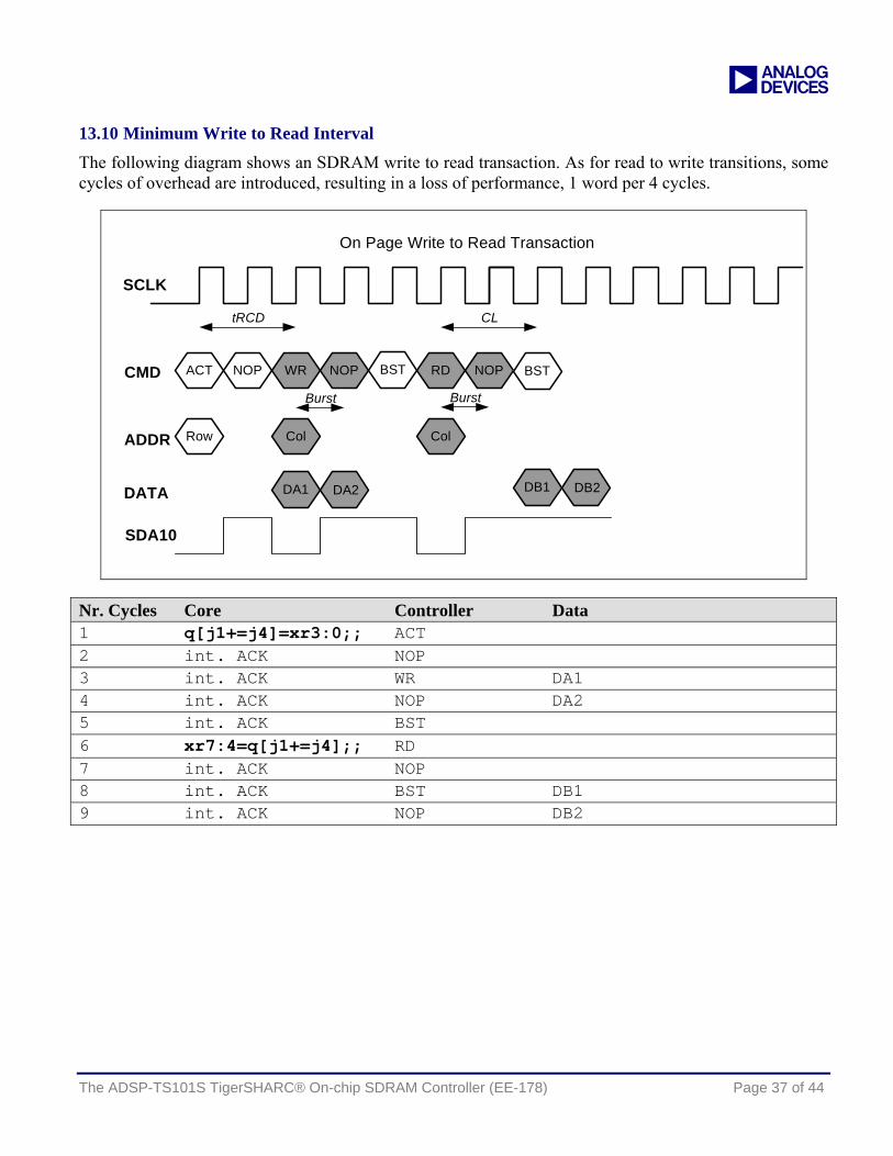
13.10 Minimum Write to Read Interval
The following diagram shows an SDRAM write to read transaction. As for read to write transitions, some cycles of overhead are introduced, resulting in a loss of performance, 1 word per 4 cycles.
SCLK
On Page Write to Read Transaction
ADDR
NOPCMD ACT WRNOP NOP RD
Row Col Col
DATA DA1
CLtRCD
Burst
DA2 DB1 DB2
BSTBST
SDA10
Burst
Nr. Cycles Core Controller Data 1 q[j1+=j4]=xr3:0;; ACT 2 int. ACK NOP 3 int. ACK WR DA1 4 int. ACK NOP DA2 5 int. ACK BST 6 xr7:4=q[j1+=j4];; RD 7 int. ACK NOP 8 int. ACK BST DB1 9 int. ACK NOP DB2
The ADSP-TS101S TigerSHARC® On-chip SDRAM Controller (EE-178) Page 37 of 44
a
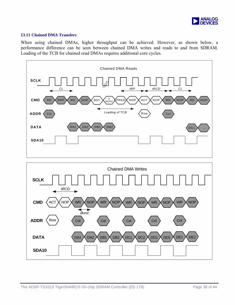
13.11 Chained DMA Transfers
When using chained DMAs, higher throughput can be achieved. However, as shown below, a performance difference can be seen between chained DMA writes and reads to and from SDRAM. Loading of the TCB for chained read DMAs requires additional core cycles.
SCLK
Chained DMA Reads
ADDR
CMD RD NOPPREA ACT NOP
DATA DA1
RD6NOPS
Row
NOP NOP
Col Col
CL tRP tRCD
BST
DA2
Loading of TCB
CL
SDA10
RD NOP
DB1 DB2 DC1 ...
RD NOP
SCLK
Chained DMA Writes
ADDR
CMD ACT WRNOP NOP WR
Row
DATA
NOP
tRCD
WR NOP WR NOP
Col Col ColCol
DB2DB1DA2DA1 DD2DD1DC2DC1
Burst
SDA10
WR NOP
Col
DE2DE1
The ADSP-TS101S TigerSHARC® On-chip SDRAM Controller (EE-178) Page 38 of 44
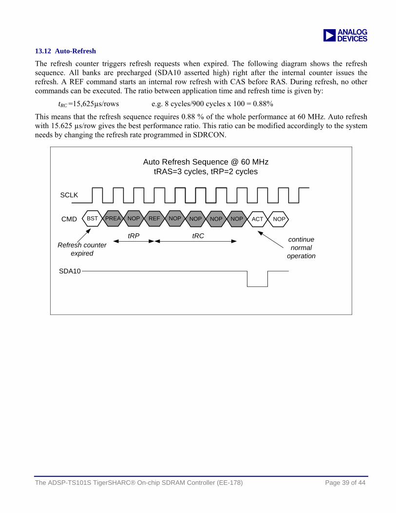
a 13.12 Auto-Refresh
The refresh counter triggers refresh requests when expired. The following diagram shows the refresh sequence. All banks are precharged (SDA10 asserted high) right after the internal counter issues the refresh. A REF command starts an internal row refresh with CAS before RAS. During refresh, no other commands can be executed. The ratio between application time and refresh time is given by:
tRC =15,625µs/rows e.g. 8 cycles/900 cycles x 100 = 0.88%
This means that the refresh sequence requires 0.88 % of the whole performance at 60 MHz. Auto refresh with 15.625 µs/row gives the best performance ratio. This ratio can be modified accordingly to the system needs by changing the refresh rate programmed in SDRCON.
SCLK
Auto Refresh Sequence @ 60 MHztRAS=3 cycles, tRP=2 cycles
Refresh counterexpired
continuenormal
operation
CMD BST NOPPREA NOP ACT NOPREF
tRP
NOP NOPNOP
tRC
SDA10
The ADSP-TS101S TigerSHARC® On-chip SDRAM Controller (EE-178) Page 39 of 44
a
13.13 Self-Refresh and Host Accesses
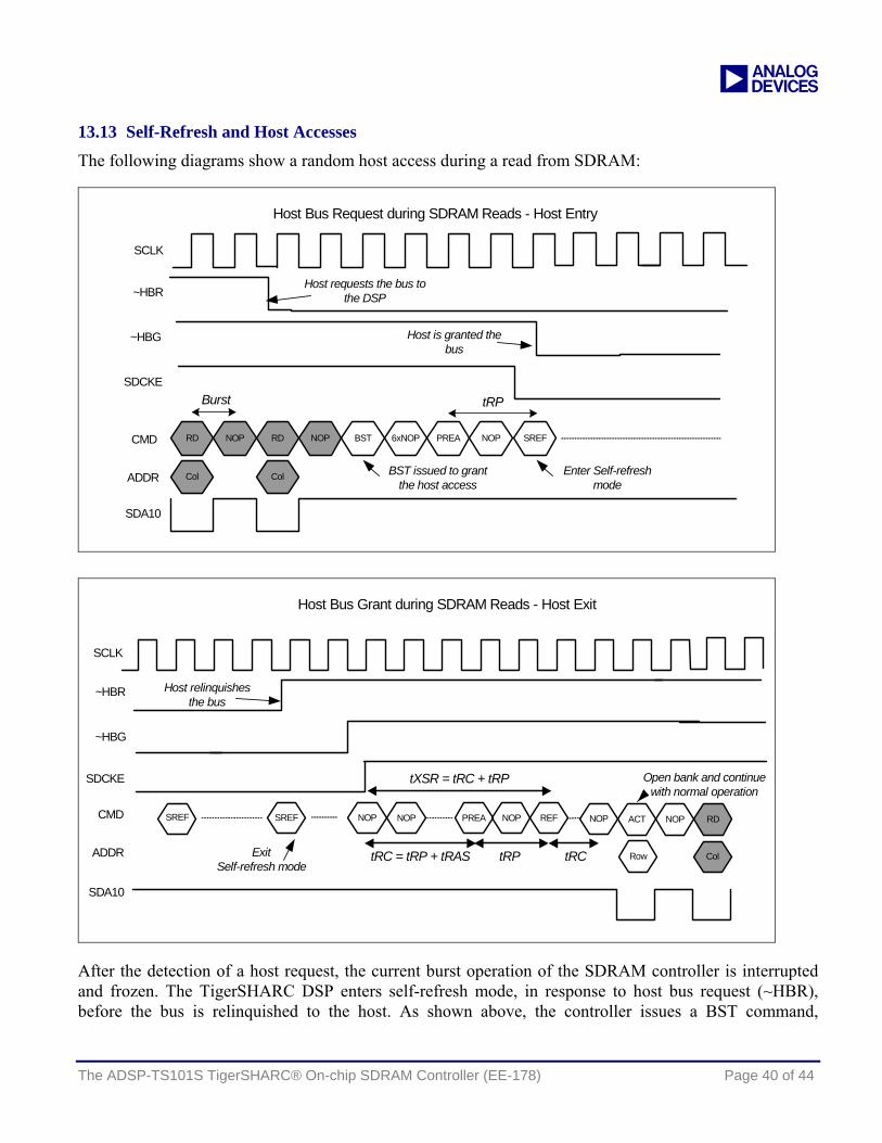
The following diagrams show a random host access during a read from SDRAM:
SCLK
Host Bus Request during SDRAM Reads - Host Entry
~HBR
ADDR
CMD
~HBG
SDA10
SDCKE
RD PREA
Col
BST 6xNOP
BST issued to grantthe host access
NOPNOP NOP SREF
Enter Self-refreshmode
RD
Col
Host requests the bus tothe DSP
Host is granted thebus
Burst tRP
SCLK
Host Bus Grant during SDRAM Reads - Host Exit
ADDR
CMD
~HBR
~HBG
SDA10
SDCKE
RD
Col
NOPSREF ACT NOP
ExitSelf-refresh mode
Row
Open bank and continuewith normal operation
Host relinquishesthe bus
SREF NOP
tRC = tRP + tRAS
PREA NOP REF
tRP
NOP
tRC
tXSR = tRC + tRP
After the detection of a host request, the current burst operation of the SDRAM controller is interrupted and frozen. The TigerSHARC DSP enters self-refresh mode, in response to host bus request (~HBR), before the bus is relinquished to the host. As shown above, the controller issues a BST command,
The ADSP-TS101S TigerSHARC® On-chip SDRAM Controller (EE-178) Page 40 of 44
a stopping the current action. In order to provide current information, all banks are precharged. During the PREA and the SREF command, the SDCKE pin transitions from high to low, thus enabling the self-refresh mode.
After deassertion of ~HBG, the controller ends the self refresh function and the SDCKE line transits high. Following, the controller issues a refresh sequence. The bank is then activated and it continues with normal operation, reading data from where it left off.
Note that only the SDCKE pin keeps control of the device in self-refresh mode.
The ADSP-TS101S TigerSHARC® On-chip SDRAM Controller (EE-178) Page 41 of 44
a
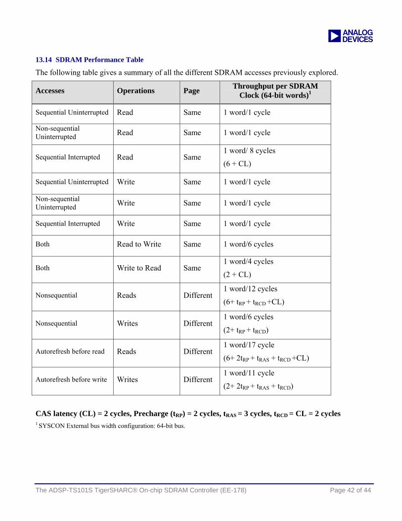
13.14 SDRAM Performance Table
The following table gives a summary of all the different SDRAM accesses previously explored.
Accesses Operations Page Throughput per SDRAM Clock (64-bit words)1
Sequential Uninterrupted Read Same 1 word/1 cycle
Non-sequential Uninterrupted Read Same 1 word/1 cycle
Sequential Interrupted Read Same 1 word/ 8 cycles
(6 + CL)
Sequential Uninterrupted Write Same 1 word/1 cycle
Non-sequential Uninterrupted Write Same 1 word/1 cycle
Sequential Interrupted Write Same 1 word/1 cycle
Both Read to Write Same 1 word/6 cycles
Both Write to Read Same 1 word/4 cycles
(2 + CL)
Nonsequential Reads Different 1 word/12 cycles
(6+ tRP + tRCD +CL)
Nonsequential Writes Different 1 word/6 cycles
(2+ tRP + tRCD)
Autorefresh before read Reads Different 1 word/17 cycle
(6+ 2tRP + tRAS + tRCD +CL)
Autorefresh before write Writes Different 1 word/11 cycle
(2+ 2tRP + tRAS + tRCD)
CAS latency (CL) = 2 cycles, Precharge (tRP) = 2 cycles, tRAS = 3 cycles, tRCD = CL = 2 cycles 1 SYSCON External bus width configuration: 64-bit bus.
The ADSP-TS101S TigerSHARC® On-chip SDRAM Controller (EE-178) Page 42 of 44
a
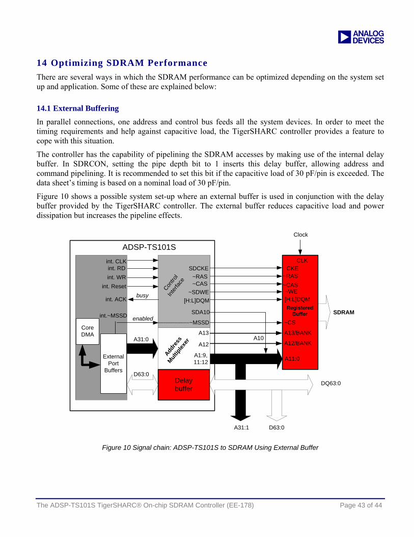
14 Optimizing SDRAM Performance There are several ways in which the SDRAM performance can be optimized depending on the system set up and application. Some of these are explained below:
14.1 External Buffering
In parallel connections, one address and control bus feeds all the system devices. In order to meet the timing requirements and help against capacitive load, the TigerSHARC controller provides a feature to cope with this situation.
The controller has the capability of pipelining the SDRAM accesses by making use of the internal delay buffer. In SDRCON, setting the pipe depth bit to 1 inserts this delay buffer, allowing address and command pipelining. It is recommended to set this bit if the capacitive load of 30 pF/pin is exceeded. The data sheet’s timing is based on a nominal load of 30 pF/pin.
Figure 10 shows a possible system set-up where an external buffer is used in conjunction with the delay buffer provided by the TigerSHARC controller. The external buffer reduces capacitive load and power dissipation but increases the pipeline effects.
SDCKE~RAS~CAS
~SDWE[H:L]DQM
SDA10
DQ63:0
int. CLKint. RDint. WR
int. Reset
int. ACK
int.~MSSD
Contro
lInt
erfac
e
ADSP-TS101S
Addre
ssMult
iplex
er
A1:9,11:12
A12
A13
~MSSD
D63:0A31:1
A31:0
enabled
busy
Delaybuffer
Clock
CLKCKE
~RAS~CAS~WE[H:L]DQM
~CS
A13/BANK
A11:0
RegisteredBuffer
A10A12/BANK
D63:0
SDRAM
CoreDMA
ExternalPort
Buffers
Figure 10 Signal chain: ADSP-TS101S to SDRAM Using External Buffer
The ADSP-TS101S TigerSHARC® On-chip SDRAM Controller (EE-178) Page 43 of 44
a 14.2 Using PC Modules
The maximum addressable size is 64Mx32-bit or 32Mx64-bit. The use of unbuffered PC DIMM modules (typical I/O sizes x32, x64, or x72 bits) is efficient, because most vendors offer a size of x64 bits, which is commonly used for PCs. Moreover, depending on the size, the need for external address- and control buffers (pipelining) is required.
14.3 General Rules for Optimized Performance
Depending on the SDRAM’s page size and number of banks, place your data segments to minimize off page and off bank accesses.
Use parallel connection for SDRAMs with big page size in order to obtain 32-bit or 64-bit I/O (SDRAM: the bigger the page size, the smaller the I/O structure).
Use the optimized settings for the controller’s state machine (tRAS, tRP, CL) depending on the speed grade and on the application’s speed
15 References [1] ADSP-TS101S TigerSHARC Processor Hardware Reference Manual. Revision 1.0, April 2003. Analog Devices Inc.
[2] ADSP-TS101S Data Sheet. Rev. A, February 2003. Analog Devices Inc
[3] The ABC of SDRAMemory (EE-126). Rev 1, March 2002. Analog Devices Inc.
[4] Understanding DMA on the ADSP-TS101S TigerSHARC (EE-143). October 2001. Analog Devices Inc.
[5] ADSP-TS101S TigerSHARC Processor Boot Loader Kernels Operation (EE-174). April 2003. Analog Devices Inc.
16 Document History
Revision Description
Rev 2 – December 19, 2003 by Maikel Kokaly-Bannourah and Robert Hoffmann
General Update and modified Address Mapping Scheme
Rev 1 – December 6, 2002 by Maikel Kokaly-Bannourah and Robert Hoffmann
Initial Release
The ADSP-TS101S TigerSHARC® On-chip SDRAM Controller (EE-178) Page 44 of 44