Embed Size (px)
Citation preview
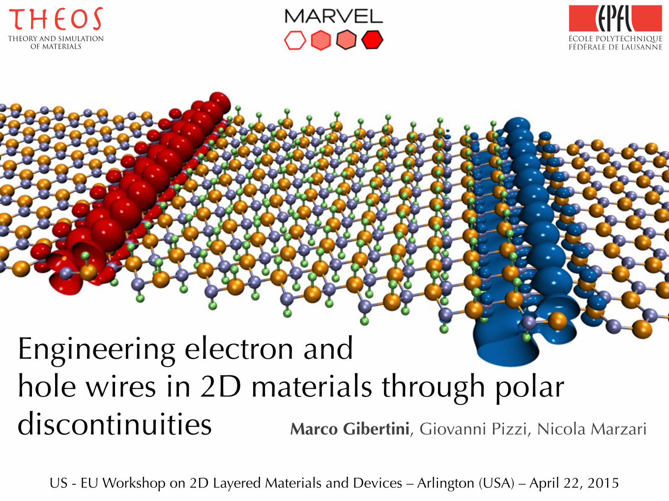
Engineering electron and hole wires in 2D materials through polar discontinuities
US - EU Workshop on 2D Layered Materials and Devices – Arlington (USA) – April 22, 2015
Marco Gibertini, Giovanni Pizzi, Nicola Marzari
THEORY AND SIMULATIONOF MATERIALS

Who are we?
(Theory and Simulation of Materials)
Swiss Federal Institute of Technology
(Lausanne, Switzerland)
Prof Nicola MarzariDr Matteo CococcioniDr Oliviero AndreussiDr Giovanni BorghiDr Marco GibertiniDr Ngoc Linh NguyenDr Giovanni Pizzi
Dr Nicolas MounetDr Ivano CastelliDr Nicola ColonnaDr Aris MarcolongoDr Martin UhrinDr James Moraes de AlmeidaDr Nicola Varini
Andrea CepellottiAnand ChandrasekaranDaniele DragoniGianluca Prandini

SWISS CENTER FOR COMPUTATIONAL DESIGN AND DISCOVERY OF NOVEL MATERIALS
Nicola Marzari, IMX, EPFLEPFL-ETHZ-UNIBAS-UNIFR-UNIGE-USI-UZH-IBM-CSCS-EMPA-PSI
The goal: Accelerated design and discovery of novel materials via a materials’ informatics platform of high-throughput quantum simulations
12-year timespan (2014-2026), and 11 Swiss Institutions: 2 Federal, 5 Cantonal, 1 Industrial, 1 Supercomputing Centre, 2 Experimental LabsFirst phase (2014-2018): 25 PIs, 34.4M CHF (18M SNSF, 6.6M EPFL, 9.8M others)
What about MARVEL?

What do we do @ ?
UNDERSTAND-PREDICT-DESIGNnovel materials and devices
from first-principles quantum simulations
•Examples for 2D materials: thermal and electrical transport
C.-H. Park, N. Bonini et al., Nano Letters 14, 1113 (2014)T. Sohier et al., Phys. Rev. B 90, 125414 (2014)
6
0 100 200 300 400T (K)
n (1013 cm−2)
Experiment(Efetov & Kim)
1.362.864.656.8510.8
0
25
50
75
100
125
150
0 100 200 300 400
! e−p
h (")
T (K)
n (1013 cm−2)
Theory
1.362.864.656.8510.8
0.1
1
10
100
10 100
! e−p
h (")
T (K)
n (1013 cm−2)
Theory
1.362.864.656.8510.8
0.1
1
10
100
10 100T (K)
n (1013 cm−2)
Experiment(Efetov & Kim)
1.362.864.656.8510.8
(b)(a)
(c) (d)
FIG. 3: Electrical resistivity of n-doped graphene arisingfrom e-ph interactions versus temperature calculated from themodel (Tab. I) incorporating e-e interaction e!ects [(a) and(c)] and the corresponding experimental data from Ref. [3][(b) and (d)]. Quantities are plotted in linear scale in (a) and(b) and in logarithmic scale in (c) and (d).
temperatures higher than those accessed in current ex-periments [3], suggesting the importance of higher tem-perature tests.
As mentioned earlier, previous theoretical studies [21,22] based on ab initio results underestimated !e-ph fromexperiments [3, 7] by ! 4 times [21] and ! 13 times [22],respectively. We attribute these discrepancies partly tothe di!erence in the calculated e-ph coupling matrix el-ements, and partly to the inclusion of e-e interaction ef-fects beyond LDA (e.g., in Ref. [22], although the velocityenhancement due to e-e interactions in the denominatorof Eq. (3) was considered, the enhancement of the e-phcoupling matrix elements and the renormalization of theA!
1 phonon frequencies [36, 37] were not considered, lead-ing to an underestimation of !e-ph).
Our main findings can thus be summarized as fol-lows: (i) The acoustic-phonon contribution to !e-ph ofthe gauge field is much more important than that ofthe deformation potential. (ii) The resistivity !e-ph aris-ing from the TA phonon modes is 2.5 times larger thanthat arising from the LA phonon modes. (iii) The high-energy optical and zone-boundary phonons in graphene("!
q " 0.150 eV) are responsible for 50% of !e-ph even atroom temperature and become dominant at higher tem-
peratures.
In conclusion, we have shown that state-of-the-art first-principles calculations employing ultra-dense Brillouinzone sampling accurately explain the charge-density andtemperature dependence of the intrinsic electrical resis-tivity of graphene and provide a detailed microscopic un-derstanding of the relative role of the di!erent phononmodes. Moreover, we have shown that it is possible tobuild an analytical model for the e-ph interactions thatretains the accuracy of ab initio calculations: this modelrepresents a useful reference for fundamental studies ofcarrier dynamics in low-dimensional graphitic systems aswell as a tool for graphene-based electronic devices sim-ulations.
! Electronic address: [email protected]† Electronic address: [email protected]
[1] M. S. Fuhrer, Physics 3, 106 (2010).[2] E. H. Hwang and S. Das Sarma, Phys. Rev. B 77, 115449
(2008).[3] D. K. Efetov and P. Kim, Phys. Rev. Lett. 105, 256805
(2010).[4] L. Pietronero, S. Strassler, H. R. Zeller, and M. J. Rice,
Phys. Rev. B 22, 904 (1980).[5] Y.-W. Tan, Y. Zhang, H. L. Stormer, and P. Kim, Eur.
Phys. J. Special Topics 148, 15 (2007).[6] S. V. Morozov, K. S. Novoselov, M. I. Katsnelson, F.
Schedin, D. C. Elias, J. A. Jaszczak, and A. K. Geim,Phys. Rev. Lett. 100, 016602 (2008).
[7] J.-H. Chen, C. Jang, S. Xiao, M. Ishigami, and M. S.Fuhrer, Nat. Nanotechnol. 3, 206 (2008).
[8] K. I. Bolotin, K. J. Sikes, J. Hone, H. L. Stormer, and P.Kim, Phys. Rev. Lett. 101, 096802 (2008).
[9] A. M. DaSilva, K. Zou, J. K. Jain, and J. Zhu, Phys.Rev. Lett. 104, 236601 (2010).
[10] E. V. Castro, H. Ochoa, M. I. Katsnelson, R. V. Gor-bachev, D. C. Elias, K. S. Novoselov, A. K. Geim, andF. Guinea, Phys. Rev. Lett. 105, 266601 (2010).
[11] E. H. Hwang and S. Das Sarma, Phys. Rev. B 79, 165404(2009).
[12] S. Fratini and F. Guinea, Phys. Rev. B 77, 195415 (2008).[13] E. Mariani and F. von Oppen, Phys. Rev. Lett. 100,
076801 (2008).[14] E. Mariani and F. von Oppen, Phys. Rev. B 82, 195403
(2010).[15] L. M. Woods and G. D. Mahan, Phys. Rev. B 61, 10651
(2000).[16] H. Suzuura and T. Ando, Phys. Rev. B 65, 235412
(2002).[17] J. L. Manes, Phys. Rev. B 76, 045430 (2007).[18] V. Perebeinos and P. Avouris, Phys. Rev. B 81, 195442
(2010).[19] F. von Oppen, F. Guinea, and E. Mariani, Phys. Rev. B
80, 075420 (2009).[20] T. Stauber, N. M. R. Peres, and F. Guinea, Phys. Rev.
B 76, 205423 (2007).[21] K. M. Borysenko, J. T. Mullen, E. A. Barry, S. Paul,
Y. G. Semenov, J. M. Zavada, M. B. Nardelli, and K. W.
•Examples for 2D materials: thermal and electrical transport•Examples for 2D materials: thermal and electrical transport
G. Fugallo, A. Cepellotti et al., Nano Letters 14, 6109 (2014)A. Cepellotti et al., Nat. Commun. 6, 6400 (2015)
0.01 0.1 1 10 100 1000L (µm)
0
1000
2000
3000
4000
k (W
/ m
K)
0% 13C1.1% 13C
T = 300 K

Design: novel devices for energy harvesting and microelectronics

Engineering polar discontinuities in 2D
Polar discontinuity across interfaces that naturally arise out of a single parent crystal using experimentally well established 2D materials
• Functionalizations
• Nanoribbons
• Grain/phase boundaries
MG, G. Pizzi, N. Marzari, Nature Communications 5, 5157 (2014)N.C. Bristowe et al., Phys. Rev. B 88, 161411 (2013)
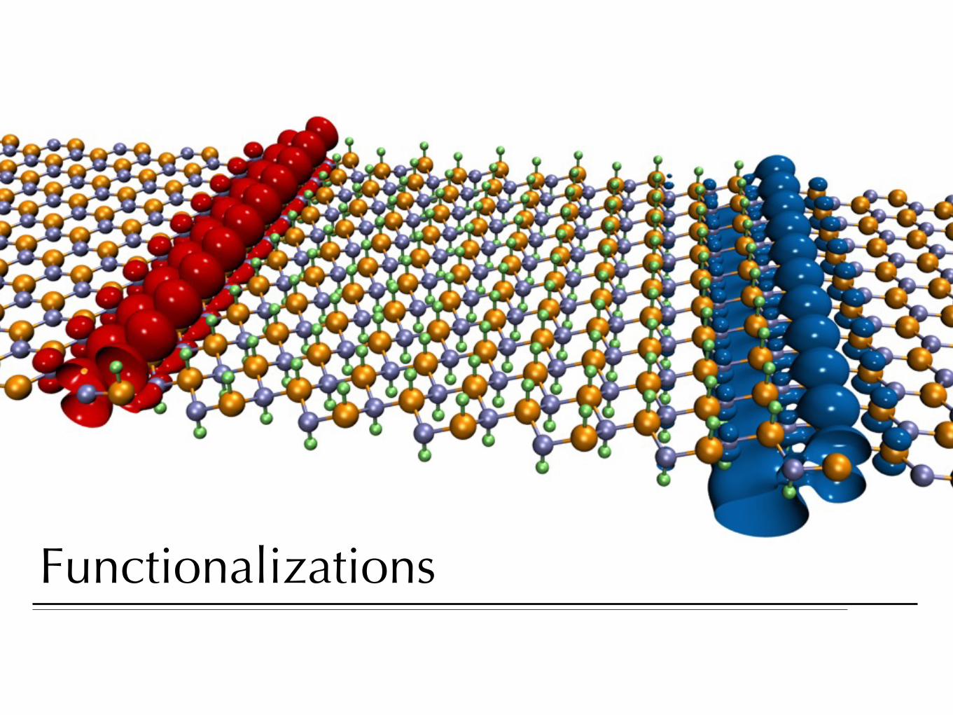
Functionalizations

Selective functionalization
Covalent functionalization with H or F changes bulk polarization
By selective functionalization we introduce a polar discontinuity
BN
BNH2
PBN = −e
a
PBNH2 = −2e
3a
BN
PBN = −e
a
–––––––
λpol = −e
3aλpol =
e
3a
+++++++

Zigzag interfaces - LDOS
0 10 20 30 40 50
Position (A)
−6
−4
−2
0
2
Energy(eV)
0.00
0.05
0.10
0.15
0.20
0.25
0.30
0.35
•The system becomes metallic
•Charge transfer from top VB to bottom CB
•Electrons and holes are localized on different interfaces
•Electric fields are present on both sides
MG, G. Pizzi, N. Marzari, Nature Communications 5, 5157 (2014)

0 50 100 150
Total width (A)
0.00
0.05
0.10
0.15
0.20
0.25
0.30
0.35
0.40
Chargedensity(e/a)
•The total free charge λF (per unit length) increases with size
λF
Zigzag interfaces - Free charge
Integrate the LDOS to get the charge density of free carriers
•Asymptotic perfect screening of polarization charge
λP = P0
BNH2− P 0
BN
λP
•Total charge at the interface
λtot = �0(|EBN|+ |EBNH2 |)
λtot

Functionalization of Graphene/BN
• Planar graphene/boron nitride heterostructures recently realized experimentally
P. Sutter et al., Nano Letters 12, 4869 (2012)Z. Liu et al., Nat. Nanotechnol. 8, 119 (2013)L. Liu et al., Science 343, 163 (2014)Y. Gong et al., Nat. Commun. 5, 4193 (2014)
• Both functionalized materials are insulating
• Polar discontinuity at the interface
• Full (instead of selective) functionalization
• Free electrons/holes appear at the interfaces
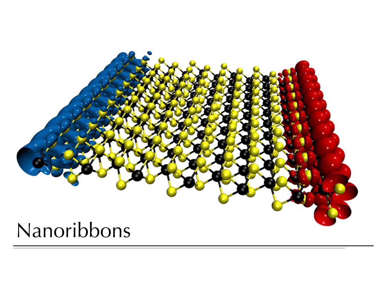
Nanoribbons

Discontinuity with vacuum: nanoribbons
Vacuum can be considered as an insulator with zero polarization
Cutting a polar 2D material into a nanoribbon creates a polar discontinuity
An electric field appears inside the nanoribbon...
...and drives an insulator-to-metal transition
free e
lectro
ns free holes
Completely different origin with respect to edge states in graphene
F. Güller,et al., Phys. Rev. B 87, 205423 (2013) MG and N. Marzari, to be submitted (2015)
10 20 30 40
Position (A)
−4
−2
0
2
4
Potentialenergy(eV)
MoS2
Possible materials: BN, MoS2 and all group-VI TMDs, etc.
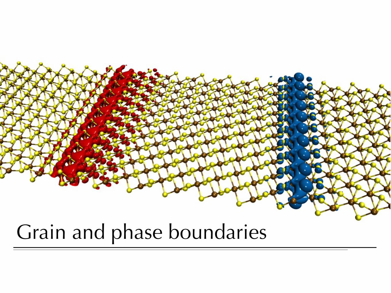
Grain and phase boundaries
X. Zou et al., Nano Lett. 13, 253 (2013) MG and N. Marzari, to be submitted
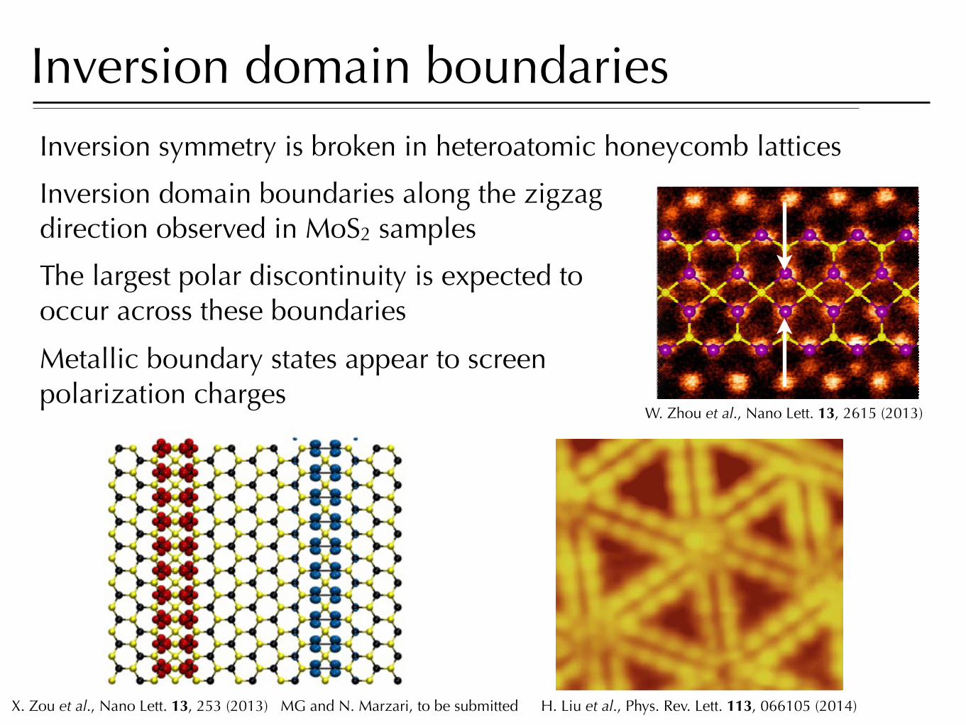
Inversion domain boundaries
Metallic boundary states appear to screen polarization charges
Inversion domain boundaries along the zigzag direction observed in MoS2 samples
W. Zhou et al., Nano Lett. 13, 2615 (2013)
10
!"#$%& '()$#*+&"', '- .$&+//"% 01) ", 2'34
!"#$ !" #$% !"#$ %&''&() 56% &'() *&+(,-
The largest polar discontinuity is expected to occur across these boundaries
Inversion symmetry is broken in heteroatomic honeycomb lattices
with the rim, i.e., along the zigzag or h1120i direction of theMoSe2 lattice.By comparing Figs. 1(a) and 1(b), we suggest that the
bright contrasts of the wagon-wheel rims in the STMimages are not topographic in origin but represent addi-tional DOS confined in 1D, as their contrasts show STMbias dependence and can sometimes disappear undercertain conditions. To elucidate this further, we performedSTS measurements, and Fig. 2(a) shows the STS spectrataken (i) far from or (ii) in the vicinity of a rim. Comparingthe two, one clearly observes extra peaks in (ii). Figure 2(b)shows a STS map (more are found in the SupplementalMaterial, Sec. 5), revealing the electronic modes confinedin 1D and interconnected into the triangular network.Intensity undulations are also apparent. As will be dis-cussed later, these metallic 1D modes are similar to theedge states of MoS2 nanoclusters [20–25], and so they canbe utilized for HDS and HER similar to nanoclusters.
In passing, we remark that spectrum (i) shows semicon-ductor characteristics ofMLMoSe2 with the energy band gapof!2.1 eV [47,48]. The opticallymeasured exciton energy inML MoSe2 was !1.6 eV [11,49,50], so our measurementwould imply an exciton binding energy of !0.5 eV, whichis consistent with the first principles calculations [51–53].To uncover the structural identity of the wagon-
wheel pattern, we performed HRTEM experiments, andFig. 3(a) shows a Fourier-filtered HRTEM image [cf. theSupplemental Material, Sec. 2] of a sample grown underthe same condition as Fig. 1 but at a smaller coverage of!1 ML. The wagon-wheel structure is again discerned inthe HRTEM micrograph. The bright rims in STM imagesnow manifest as the darker boundaries separating domains
FIG. 2 (color online). STS spectra and calculated DOS of theIDB defect. (a) STS spectra of ML MoSe2 at the points as markedby the crosses in (b), i.e., (i) away from or (ii) in the vicinityof a defect. (b) A STS map (size: 8.6 ! 8.6 nm2) obtained atVsample ! !0.42 eV, showing the 1D defect modes and theirintensity undulations along the lengths of the defects. (c),(d) Cal-culated DOS and the band structure. The red and green dots in (d)represent states from Mo and Se atoms at the core of the defect,respectively, and the dotted blue states are from Mo next to thecore. In (c), the red-shaded regions are the valence and conductionbands of bulk ML MoSe2 and the black line is the DOS from thedefect. (e),(f) STS maps obtained at Vsample ! !1.85 and 0.72 eV,respectively, superimposed with the calculated DOS maps andthe ball model of the structure [refer to Fig. 3(d) below] at thecorresponding energies. The calculated maps represent the centralregion of a larger ribbon model (cf. the Supplemental Material,Sec. 3), showing the DOS of the defect.
FIG. 1 (color online). STM micrographs of MoSe2 on HOPG.(a) Topographic image (size: 80 ! 80 nm2, sample biasVsample ! 2.0 V) of a 1.4 MLMoSe2 film. The white arrows pointto the exposed substrate (1) and the second (2) and third (3) layerMoSe2 islands, respectively. The inset is the reflection high-energyelectron diffraction pattern taken along [1120]. (b) Topographicimage of the same area as (a) but at Vsample ! !1.0 V. (c),(d) Close-up STM images [size: 35 ! 35 nm2, Vsample ! !1.0Vfor (c); 13 ! 13 nm2 and Vsample ! !1.46 V for (d)], revealingthe wagon-wheel patterns and the intensity undulations. (e) STMimage (size: 9.2 ! 9.2 nm2, Vsample ! !1.78 V) showing themoiré pattern, e.g., in the upper-left corner of the micrograph.The inset is the intensity profile along the white line, showing theperiod of the moiré pattern to be of !1 nm.
PRL 113, 066105 (2014) P HY S I CA L R EV I EW LE T T ER Sweek ending
8 AUGUST 2014
066105-2
H. Liu et al., Phys. Rev. Lett. 113, 066105 (2014)
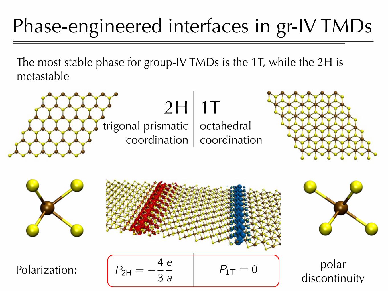
Phase-engineered interfaces in gr-IV TMDs
The most stable phase for group-IV TMDs is the 1T, while the 2H is metastable
Polarization:
2Htrigonal prismatic
coordination
1Toctahedral coordination
P2H = −4
3
e
aP1T = 0
insulatinginsulating
TiS2 ✓ ✓ TiS2
TiSe2 ! ! TiSe2
ZrS2 ✓ ✓ ZrS2
ZrSe2 ✓ ✓ ZrSe2
HfS2 ✓ ✓ HfS2
HfSe2 ✓ ✓ HfSe2
polar discontinuity
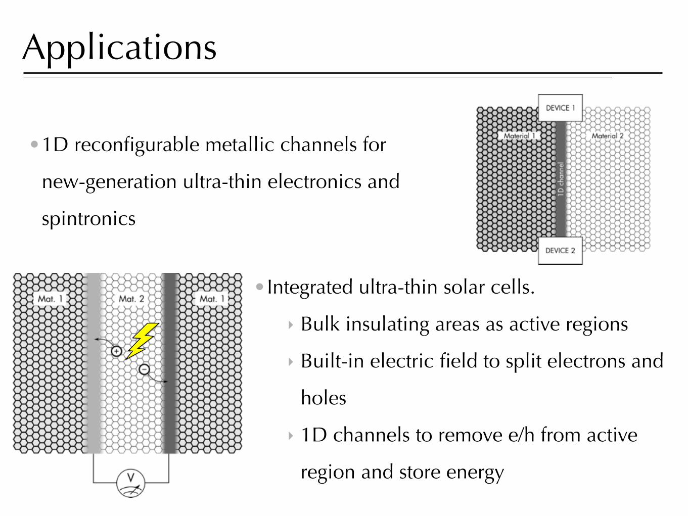
Applications
•1D reconfigurable metallic channels for
new-generation ultra-thin electronics and
spintronics
•Integrated ultra-thin solar cells.
‣ Bulk insulating areas as active regions
‣ Built-in electric field to split electrons and
holes
‣ 1D channels to remove e/h from active
region and store energy
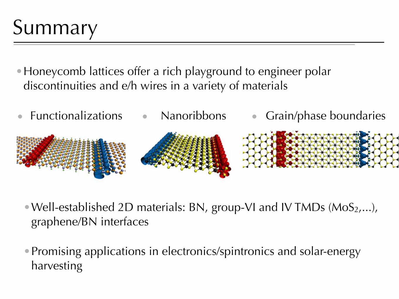
Summary
•Honeycomb lattices offer a rich playground to engineer polar discontinuities and e/h wires in a variety of materials
•Promising applications in electronics/spintronics and solar-energy harvesting
• Functionalizations • Nanoribbons • Grain/phase boundaries
•Well-established 2D materials: BN, group-VI and IV TMDs (MoS2,...), graphene/BN interfaces