Embed Size (px)
Citation preview
Engr 241/ Fall 2017Advanced Micro- & Nano- Fabrication Laboratory
Stanford Nanofabrication Facility
Your presenters for today
Jon Fan – Faculty Director of ExFab and instructor for E241Eric Wu – Grad student, Howe group, E241/Fall ‘16 alumnusKaren Dowling – Grad student, Senesky group, E241/Fall ’16 alumnusSNF Staff: Swaroop Kommera
Carsen KlineXiaoqing XuMichelle RinconUsha RaghuramMary Tang
2
Outline
• What is ExFab? • What is E241?• ExFab equipment and capabilities
3
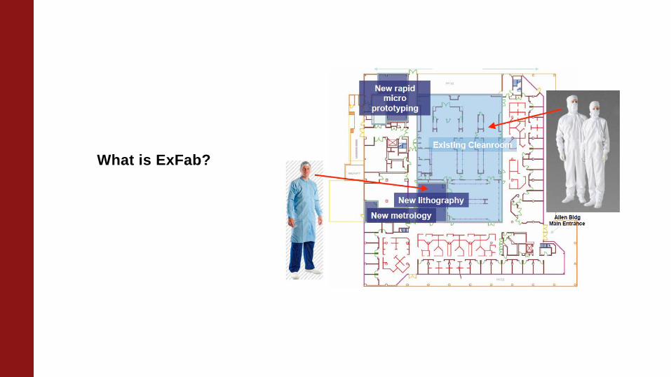
What is ExFab?
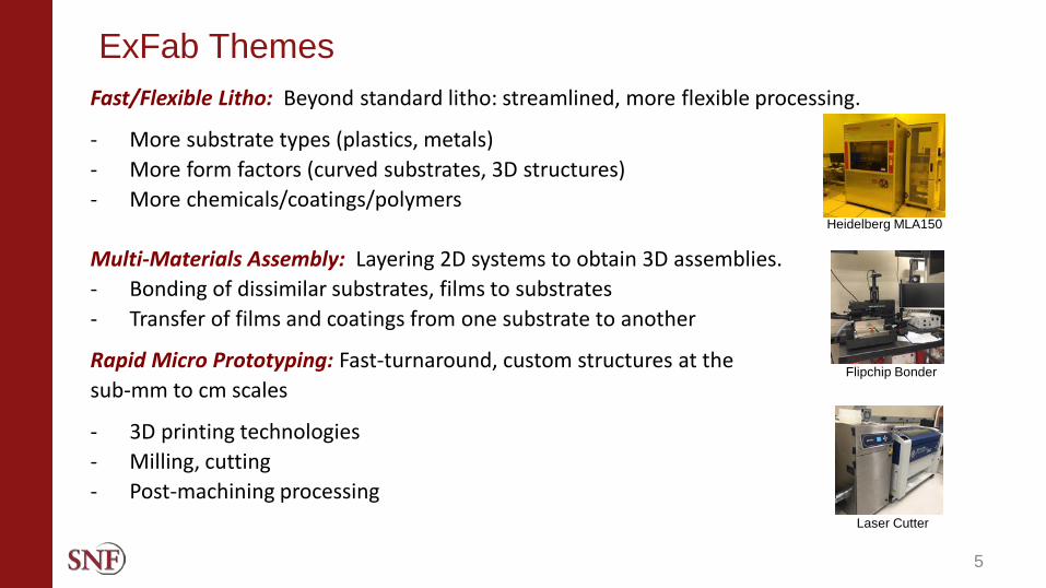
ExFab Themes
5
Fast/Flexible Litho: Beyond standard litho: streamlined, more flexible processing.
- More substrate types (plastics, metals)- More form factors (curved substrates, 3D structures)- More chemicals/coatings/polymers
Multi-Materials Assembly: Layering 2D systems to obtain 3D assemblies.- Bonding of dissimilar substrates, films to substrates- Transfer of films and coatings from one substrate to another
Rapid Micro Prototyping: Fast-turnaround, custom structures at the sub-mm to cm scales
- 3D printing technologies- Milling, cutting- Post-machining processing
Heidelberg MLA150
Flipchip Bonder
Laser Cutter
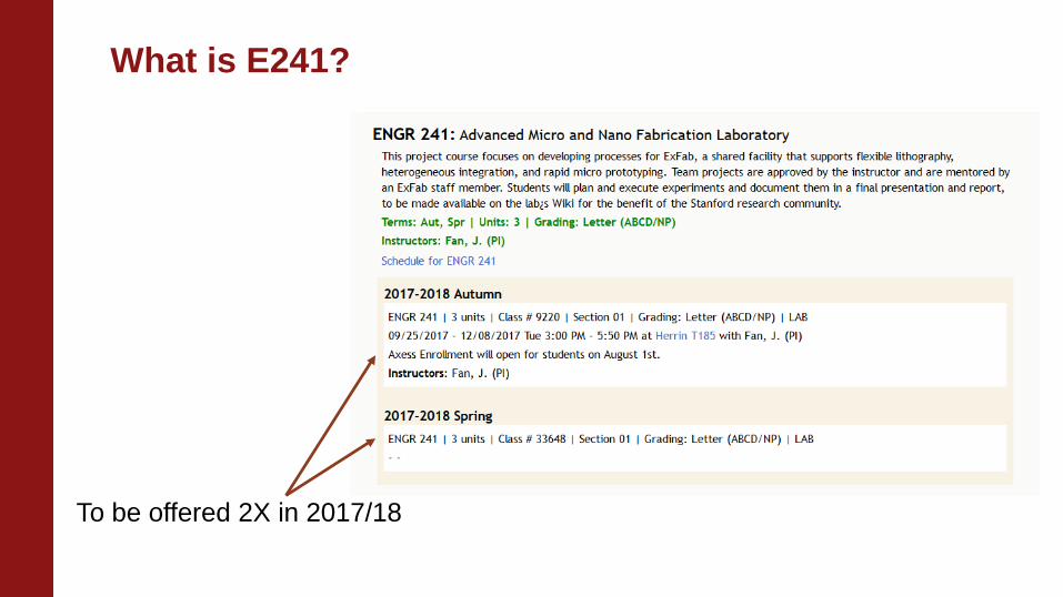
What is E241?
To be offered 2X in 2017/18
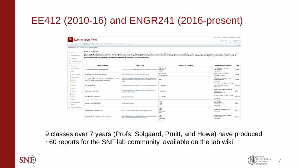
EE412 (2010-16) and ENGR241 (2016-present)
7
9 classes over 7 years (Profs. Solgaard, Pruitt, and Howe) have produced ~60 reports for the SNF lab community, available on the lab wiki.
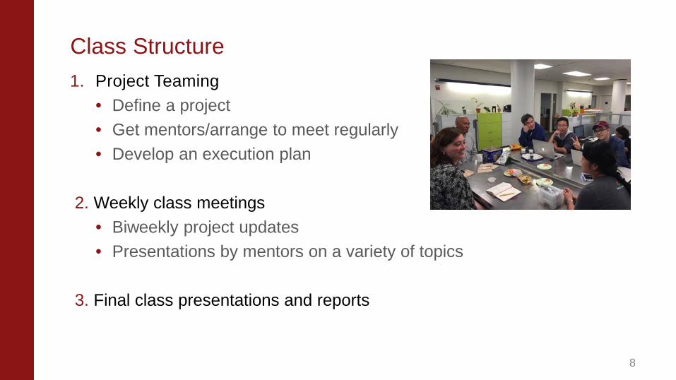
Class Structure1. Project Teaming
• Define a project• Get mentors/arrange to meet regularly• Develop an execution plan
2. Weekly class meetings• Biweekly project updates• Presentations by mentors on a variety of topics
3. Final class presentations and reports
8
Ground rules
9
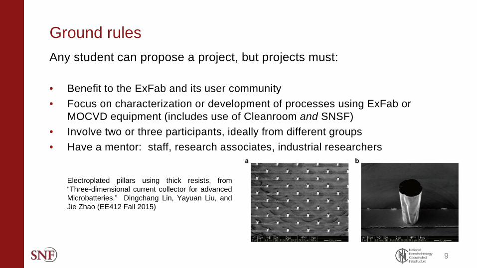
Electroplated pillars using thick resists, from“Three-dimensional current collector for advancedMicrobatteries.” Dingchang Lin, Yayuan Liu, andJie Zhao (EE412 Fall 2015)
Any student can propose a project, but projects must:
• Benefit to the ExFab and its user community• Focus on characterization or development of processes using ExFab or
MOCVD equipment (includes use of Cleanroom and SNSF)• Involve two or three participants, ideally from different groups• Have a mentor: staff, research associates, industrial researchers
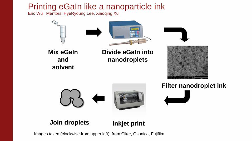
Divide eGaIn into nanodroplets
Mix eGaInand
solvent
Inkjet printJoin droplets Images taken (clockwise from upper left) from Clker, Qsonica, Fujifilm
Printing eGaIn like a nanoparticle inkEric Wu Mentors: HyeRyoung Lee, Xiaoqing Xu
Filter nanodroplet ink
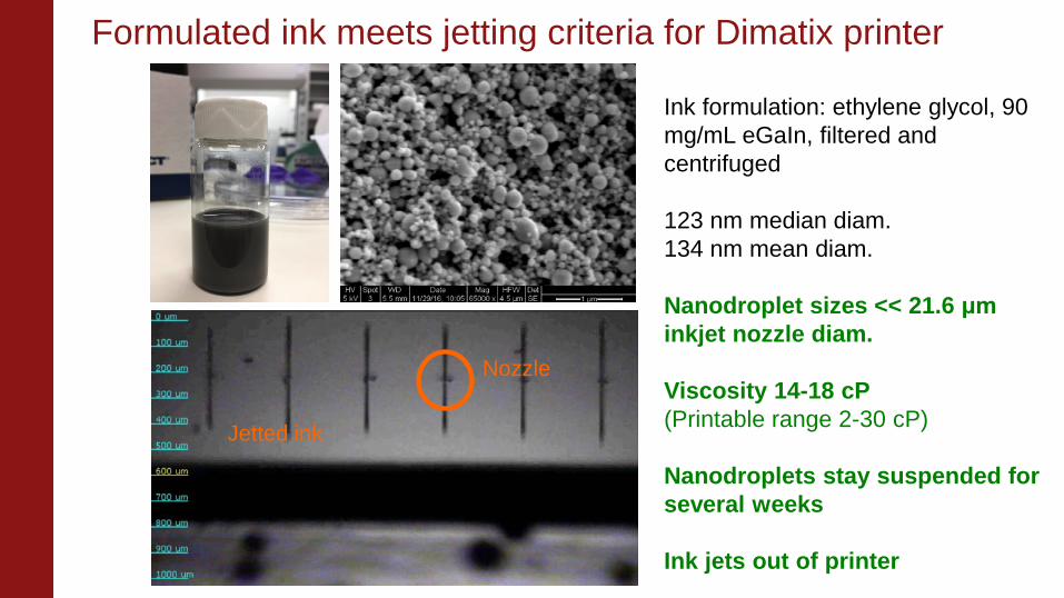
Formulated ink meets jetting criteria for Dimatix printer
Ink formulation: ethylene glycol, 90 mg/mL eGaIn, filtered and centrifuged
123 nm median diam.134 nm mean diam.
Nanodroplet sizes << 21.6 μminkjet nozzle diam.
Viscosity 14-18 cP(Printable range 2-30 cP)
Nanodroplets stay suspended for several weeks
Ink jets out of printer
Nozzle
Jetted ink
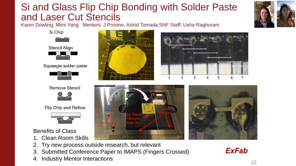
Si and Glass Flip Chip Bonding with Solder Paste and Laser Cut StencilsKaren Dowling, Mimi Yang Mentors: J Provine, Astrid Tomada SNF Staff: Usha Raghuram
12
Benefits of Class1. Clean Room Skills2. Try new process outside research, but relevant3. Submitted Conference Paper to IMAPS (Fingers Crossed)4. Industry Mentor Interactions
E241 Mentors 2017
13
Illustrious mentors 2017 (many returning from 2016)!
Tony Ricco – Chief Technologist at NASA Ames, on leave from StanfordKim Harrison – Researcher/Consultant Dave Huber – Senior Research Engineer, SRIRoozbeh Parsa – General Manager at TIVijay Narashimhan – Researcher at IntermolecularHye Ryoung Lee – Research Associate, Yi Cui labJ Provine – Researcher/ConsultantChristian Gutierrez – Researcher at GoogleXMark Zdeblick – CTO/Co-Founder of Proteus Digital HealthMike Robles – Researcher at Calico Labs
… plus the SNF and SNSF Staff (Shiva, Swaroop, Usha, Xiaoqing, Carsen, Michelle, Maurice)
If you would like to be a mentor or know someone who might be interested in being one, contact Mary, Jon, or other staff member.
Benefits of participation: Why should you join E241?
You get:
• to focus on a project that will benefit YOUR research ... and that of others
• equipment use at no cost to your research project• access to the collective expertise of mentors,
instructors, staff, and equipment providers.• CLASS CREDIT• the satisfaction of supporting the Fab community
14
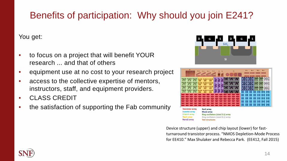
Device structure (upper) and chip layout (lower) for fast-turnaround transistor process. “NMOS Depletion-Mode Process for EE410.” Max Shulaker and Rebecca Park. (EE412, Fall 2015)
How to participate in E241
15
• Enroll! • Enrollment is capped at 20• Instructor-selected project teams
of 2 or 3 each 8-10 projects
• Mentor!!• With instructor approval, ANYONE
can be a mentor (post-doc, grad, visiting scholar, industry, etc.)
• Support your lab mates!• Come to the final presentations
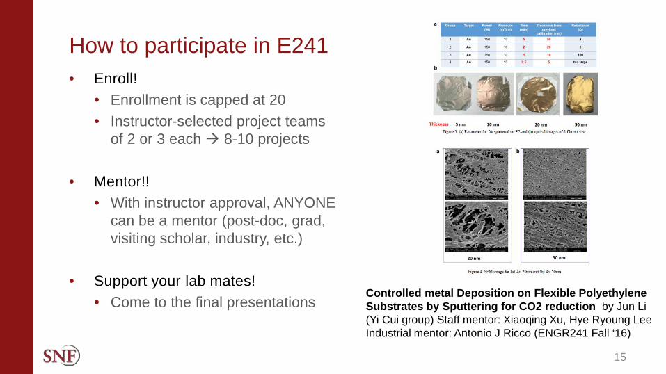
Controlled metal Deposition on Flexible Polyethylene Substrates by Sputtering for CO2 reduction by Jun Li (Yi Cui group) Staff mentor: Xiaoqing Xu, Hye Ryoung Lee Industrial mentor: Antonio J Ricco (ENGR241 Fall ‘16)
E X FA B E Q U I P M E N T
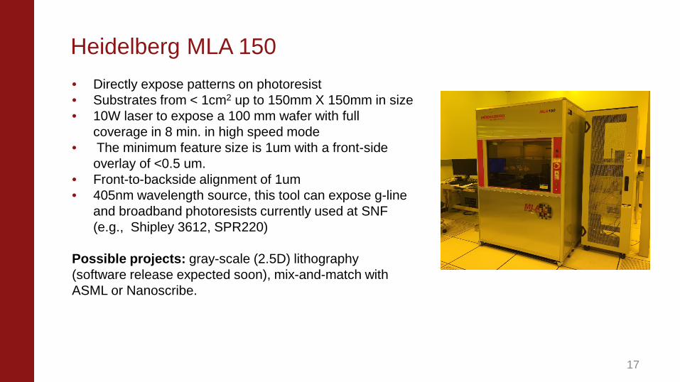
Heidelberg MLA 150
17
• Directly expose patterns on photoresist • Substrates from < 1cm2 up to 150mm X 150mm in size• 10W laser to expose a 100 mm wafer with full
coverage in 8 min. in high speed mode• The minimum feature size is 1um with a front-side
overlay of <0.5 um. • Front-to-backside alignment of 1um • 405nm wavelength source, this tool can expose g-line
and broadband photoresists currently used at SNF (e.g., Shipley 3612, SPR220)
Possible projects: gray-scale (2.5D) lithography (software release expected soon), mix-and-match with ASML or Nanoscribe.
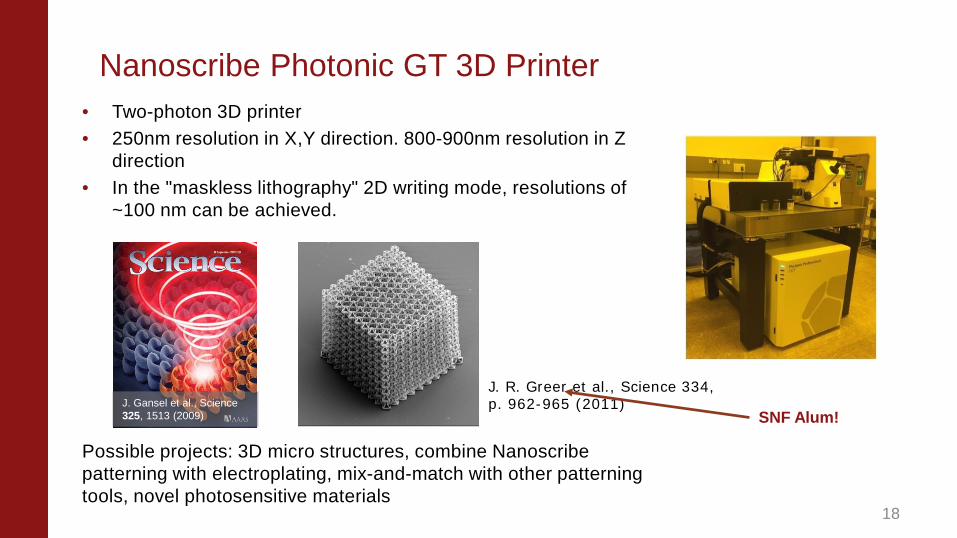
Nanoscribe Photonic GT 3D Printer
18
• Two-photon 3D printer • 250nm resolution in X,Y direction. 800-900nm resolution in Z
direction• In the "maskless lithography" 2D writing mode, resolutions of
~100 nm can be achieved.
Possible projects: 3D micro structures, combine Nanoscribe patterning with electroplating, mix-and-match with other patterning tools, novel photosensitive materials
J. R. Greer et al., Science 334, p. 962-965 (2011)
SNF Alum!J. Gansel et al., Science 325, 1513 (2009)
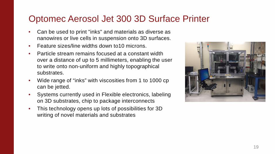
Optomec Aerosol Jet 300 3D Surface Printer
19
• Can be used to print "inks" and materials as diverse as nanowires or live cells in suspension onto 3D surfaces.
• Feature sizes/line widths down to10 microns. • Particle stream remains focused at a constant width
over a distance of up to 5 millimeters, enabling the user to write onto non-uniform and highly topographical substrates.
• Wide range of “inks” with viscosities from 1 to 1000 cpcan be jetted.
• Systems currently used in Flexible electronics, labeling on 3D substrates, chip to package interconnects
• This technology opens up lots of possibilities for 3D writing of novel materials and substrates
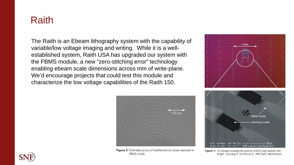
Raith
The Raith is an Ebeam lithography system with the capability of variable/low voltage imaging and writing. While it is a well-established system, Raith USA has upgraded our system with the FBMS module, a new “zero-stitching error” technology enabling ebeam scale dimensions across mm of write-plane. We’d encourage projects that could test this module and characterize the low voltage capabilities of the Raith 150.
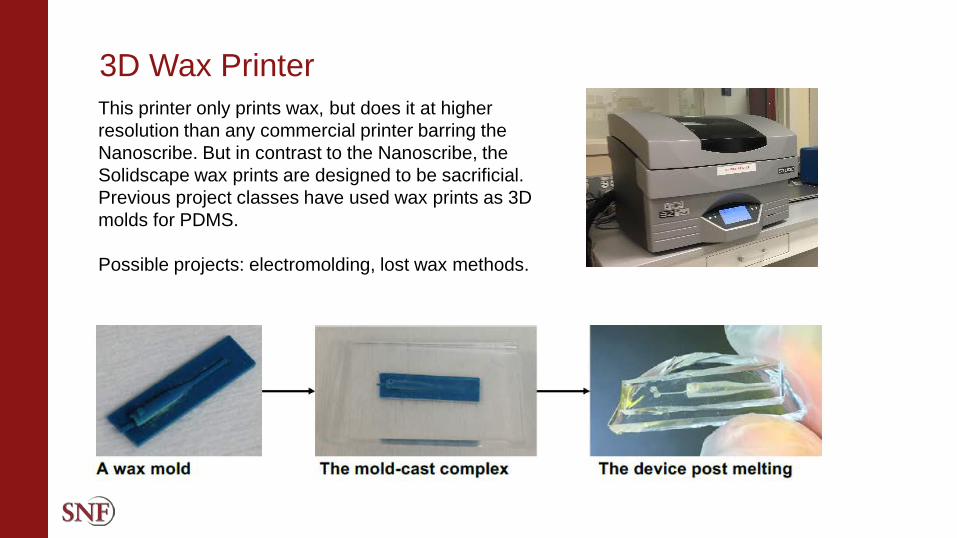
3D Wax PrinterThis printer only prints wax, but does it at higher resolution than any commercial printer barring the Nanoscribe. But in contrast to the Nanoscribe, the Solidscape wax prints are designed to be sacrificial. Previous project classes have used wax prints as 3D molds for PDMS.
Possible projects: electromolding, lost wax methods.
Lesker-sputter
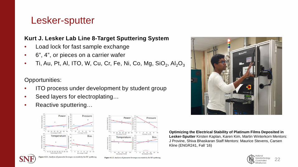
Kurt J. Lesker Lab Line 8-Target Sputtering System• Load lock for fast sample exchange• 6”, 4”, or pieces on a carrier wafer• Ti, Au, Pt, Al, ITO, W, Cu, Cr, Fe, Ni, Co, Mg, SiO2, Al2O3
Opportunities:• ITO process under development by student group• Seed layers for electroplating… • Reactive sputtering…
22
Optimizing the Electrical Stability of Platinum Films Deposited in Lesker-Sputter Kirsten Kaplan, Karen Kim, Martin Winterkorn Mentors: J Provine, Shiva Bhaskaran Staff Mentors: Maurice Stevens, Carsen Kline (ENGR241, Fall ‘16)
Aix-CCS GaN MOCVD
23
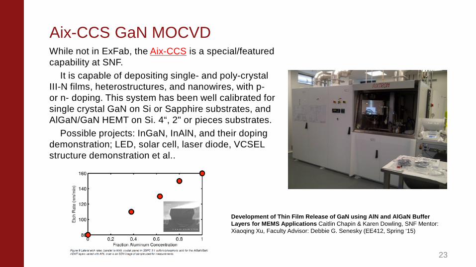
While not in ExFab, the Aix-CCS is a special/featured capability at SNF.
It is capable of depositing single- and poly-crystal III-N films, heterostructures, and nanowires, with p-or n- doping. This system has been well calibrated for single crystal GaN on Si or Sapphire substrates, and AlGaN/GaN HEMT on Si. 4“, 2" or pieces substrates.
Possible projects: InGaN, InAlN, and their doping demonstration; LED, solar cell, laser diode, VCSEL structure demonstration et al..
Development of Thin Film Release of GaN using AlN and AlGaN Buffer Layers for MEMS Applications Caitlin Chapin & Karen Dowling, SNF Mentor: Xiaoqing Xu, Faculty Advisor: Debbie G. Senesky (EE412, Spring ‘15)
CNT Furnace
24
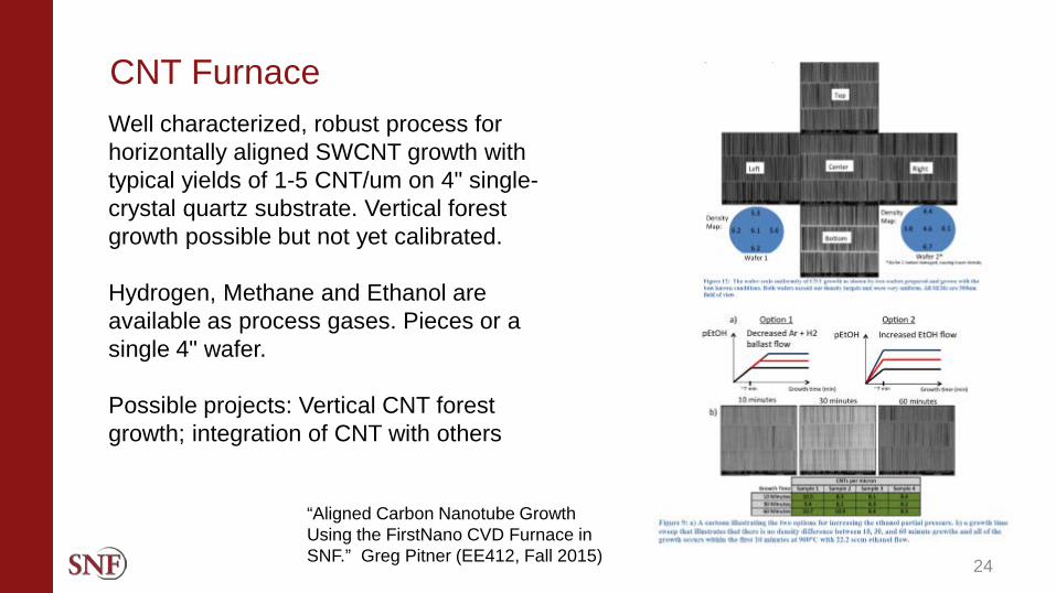
Well characterized, robust process for horizontally aligned SWCNT growth with typical yields of 1-5 CNT/um on 4" single-crystal quartz substrate. Vertical forest growth possible but not yet calibrated.
Hydrogen, Methane and Ethanol are available as process gases. Pieces or a single 4" wafer.
Possible projects: Vertical CNT forest growth; integration of CNT with others
“Aligned Carbon Nanotube Growth Using the FirstNano CVD Furnace in SNF.” Greg Pitner (EE412, Fall 2015)
Graphene Furnace
25
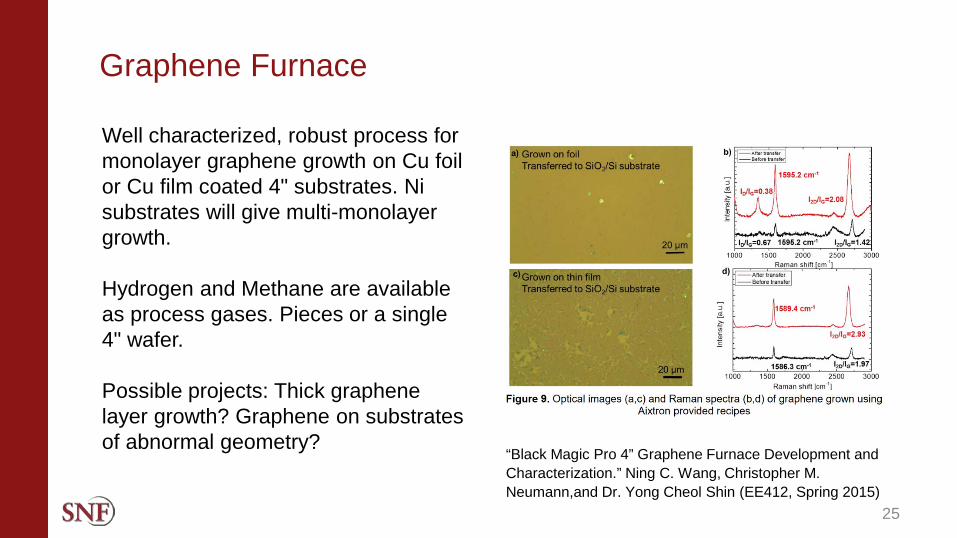
Well characterized, robust process for monolayer graphene growth on Cu foil or Cu film coated 4" substrates. Ni substrates will give multi-monolayer growth.
Hydrogen and Methane are available as process gases. Pieces or a single 4" wafer.
Possible projects: Thick graphene layer growth? Graphene on substrates of abnormal geometry?
“Black Magic Pro 4” Graphene Furnace Development and Characterization.” Ning C. Wang, Christopher M. Neumann,and Dr. Yong Cheol Shin (EE412, Spring 2015)
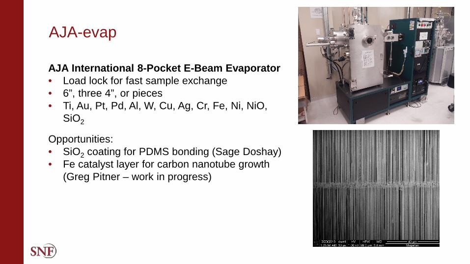
AJA-evap
AJA International 8-Pocket E-Beam Evaporator• Load lock for fast sample exchange• 6”, three 4”, or pieces• Ti, Au, Pt, Pd, Al, W, Cu, Ag, Cr, Fe, Ni, NiO,
SiO2
Opportunities:• SiO2 coating for PDMS bonding (Sage Doshay)• Fe catalyst layer for carbon nanotube growth
(Greg Pitner – work in progress)
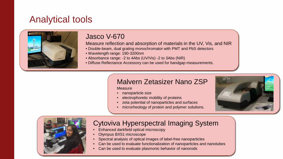
Analytical tools
Jasco V-670Measure reflection and absorption of materials in the UV, Vis, and NIR• Double-beam, dual grating monochromator with PMT and PbS detectors• Wavelength range: 190-3200nm• Absorbance range: -2 to 4Abs (UV/Vis) -2 to 3Abs (NIR)• Diffuse Reflectance Accessory can be used for bandgap measurements.
Malvern Zetasizer Nano ZSPMeasure • nanoparticle size• electrophoretic mobility of proteins• zeta potential of nanoparticles and surfaces• microrheology of protein and polymer solutions.
Cytoviva Hyperspectral Imaging System• Enhanced darkfield optical microscopy• Olympus BX51 microscope• Spectral analysis of optical images of label-free nanoparticles• Can be used to evaluate functionalization of nanoparticles and nanotubes• Can be used to evaluate plasmonic behavior of nanorods
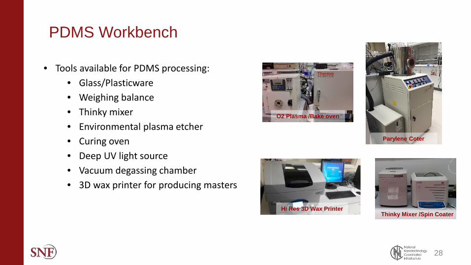
PDMS Workbench
28
• Tools available for PDMS processing:• Glass/Plasticware• Weighing balance • Thinky mixer• Environmental plasma etcher• Curing oven• Deep UV light source• Vacuum degassing chamber • 3D wax printer for producing masters
Thinky Mixer /Spin Coater
O2 Plasma /Bake oven
Parylene Coter
Hi Res 3D Wax Printer
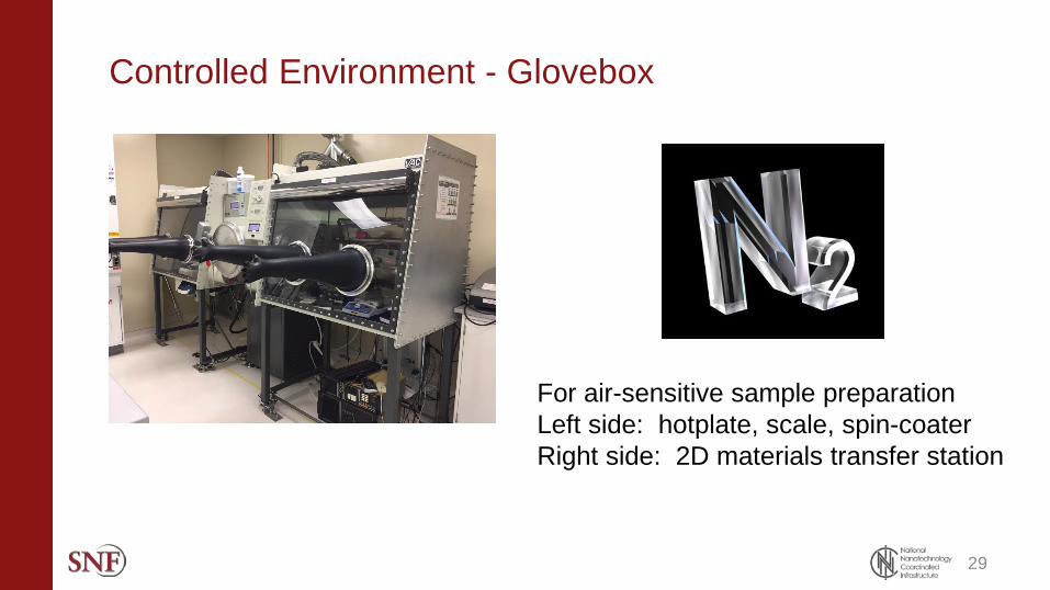
Controlled Environment - Glovebox
29
For air-sensitive sample preparationLeft side: hotplate, scale, spin-coaterRight side: 2D materials transfer station
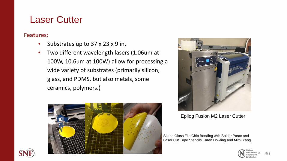
Laser Cutter
30
Features:• Substrates up to 37 x 23 x 9 in.• Two different wavelength lasers (1.06um at
100W, 10.6um at 100W) allow for processing a wide variety of substrates (primarily silicon, glass, and PDMS, but also metals, some ceramics, polymers.)
Epilog Fusion M2 Laser Cutter
Si and Glass Flip Chip Bonding with Solder Paste and Laser Cut Tape Stencils Karen Dowling and Mimi Yang
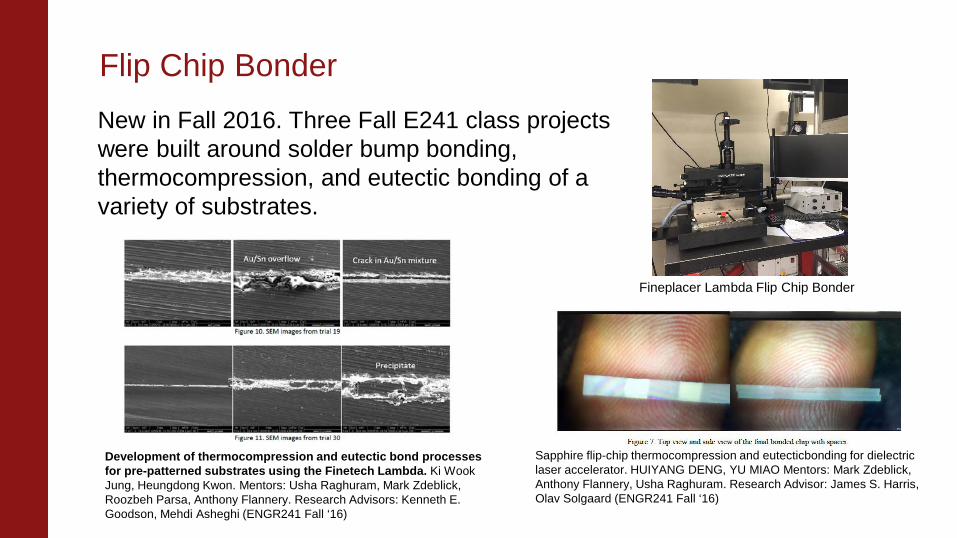
Flip Chip BonderNew in Fall 2016. Three Fall E241 class projects were built around solder bump bonding, thermocompression, and eutectic bonding of a variety of substrates.
Fineplacer Lambda Flip Chip Bonder
Sapphire flip-chip thermocompression and eutecticbonding for dielectric laser accelerator. HUIYANG DENG, YU MIAO Mentors: Mark Zdeblick, Anthony Flannery, Usha Raghuram. Research Advisor: James S. Harris, Olav Solgaard (ENGR241 Fall ‘16)
Development of thermocompression and eutectic bond processes for pre-patterned substrates using the Finetech Lambda. Ki WookJung, Heungdong Kwon. Mentors: Usha Raghuram, Mark Zdeblick, Roozbeh Parsa, Anthony Flannery. Research Advisors: Kenneth E. Goodson, Mehdi Asheghi (ENGR241 Fall ‘16)
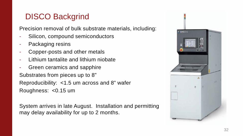
DISCO BackgrindPrecision removal of bulk substrate materials, including:- Silicon, compound semiconductors- Packaging resins- Copper-posts and other metals- Lithium tantalite and lithium niobate- Green ceramics and sapphireSubstrates from pieces up to 8”Reproducibility: <1.5 um across and 8” waferRoughness: <0.15 um
System arrives in late August. Installation and permitting may delay availability for up to 2 months.
32
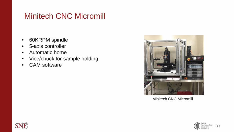
Minitech CNC Micromill
33
• 60KRPM spindle• 5-axis controller• Automatic home• Vice/chuck for sample holding• CAM software
Minitech CNC Micromill
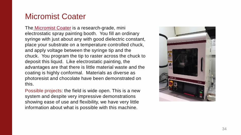
Micromist CoaterThe Micromist Coater is a research-grade, mini electrostatic spray painting booth. You fill an ordinary syringe with just about any with good dielectric constant, place your substrate on a temperature controlled chuck, and apply voltage between the syringe tip and the chuck. You program the tip to raster across the chuck to deposit this liquid. Like electrostatic painting, the advantages are that there is little material waste and the coating is highly conformal. Materials as diverse as photoresist and chocolate have been demonstrated on this. Possible projects: the field is wide open. This is a new system and despite very impressive demonstrations showing ease of use and flexibility, we have very little information about what is possible with this machine.
34
35
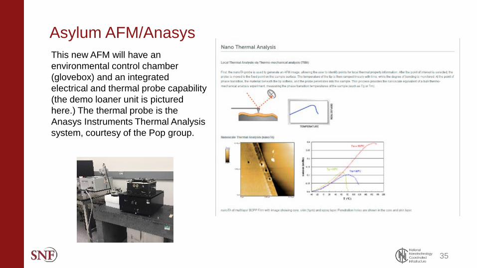
This new AFM will have an environmental control chamber (glovebox) and an integrated electrical and thermal probe capability (the demo loaner unit is pictured here.) The thermal probe is the Anasys Instruments Thermal Analysis system, courtesy of the Pop group.
Asylum AFM/Anasys
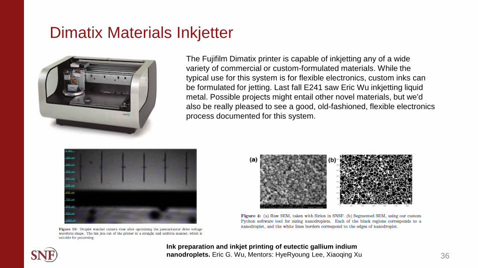
Dimatix Materials Inkjetter
36
The Fujifilm Dimatix printer is capable of inkjetting any of a wide variety of commercial or custom-formulated materials. While the typical use for this system is for flexible electronics, custom inks can be formulated for jetting. Last fall E241 saw Eric Wu inkjetting liquid metal. Possible projects might entail other novel materials, but we'd also be really pleased to see a good, old-fashioned, flexible electronics process documented for this system.
Ink preparation and inkjet printing of eutectic gallium indium nanodroplets. Eric G. Wu, Mentors: HyeRyoung Lee, Xiaoqing Xu