Embed Size (px)
Citation preview

MSP430™
Value Line MCUs
Enhance simple analog and digital functions for $0.25
SWAB003B

Texa
s In
stru
men
ts
2
Table of contents
Introduction . . . . . . . . . . . . . . . . . . . . . . . . . . . . . . . . . . . . . . . . . . 3
Communication functions
Single-wire communication host . . . . . . . . . . . . . . . . . . . . . . . . . . . 6
UART-to-UART bridge . . . . . . . . . . . . . . . . . . . . . . . . . . . . . . . . . . . 8
UART-to-SPI bridge . . . . . . . . . . . . . . . . . . . . . . . . . . . . . . . . . . . . 10
SPI IO expander . . . . . . . . . . . . . . . . . . . . . . . . . . . . . . . . . . . . . . . 12
Pulse width modulation (PWM) functions
UART software-controlled RGB LED color mixing . . . . . . . . . . . . . 14
Servo motor control . . . . . . . . . . . . . . . . . . . . . . . . . . . . . . . . . . . . 16
Stepper motor control . . . . . . . . . . . . . . . . . . . . . . . . . . . . . . . . . . 18
Dual output, 8-Bit PWM DAC . . . . . . . . . . . . . . . . . . . . . . . . . . . . . 20
Analog input to PWM output . . . . . . . . . . . . . . . . . . . . . . . . . . . . . 24
System and housekeeping functions
EEPROM emulation . . . . . . . . . . . . . . . . . . . . . . . . . . . . . . . . . . . . 26
Low power hex keypad . . . . . . . . . . . . . . . . . . . . . . . . . . . . . . . . . 28
Multi-function reset controller . . . . . . . . . . . . . . . . . . . . . . . . . . . . 30
Quadrature encoder position counter . . . . . . . . . . . . . . . . . . . . . . 32
Single slope analog-to-digital conversion technique . . . . . . . . . . 36
ADC Wake and Transmit on Threshold . . . . . . . . . . . . . . . . . . . . . 38
Hysteresis comparator with UART . . . . . . . . . . . . . . . . . . . . . . . . . 40
Tamper detection . . . . . . . . . . . . . . . . . . . . . . . . . . . . . . . . . . . . . . 42
Programmable frequency locked loop . . . . . . . . . . . . . . . . . . . . . 46
Programmable clock source . . . . . . . . . . . . . . . . . . . . . . . . . . . . . 50
Timer functions
External RTC with backup memory . . . . . . . . . . . . . . . . . . . . . . . . 52
Programmable system wake-up controller . . . . . . . . . . . . . . . . . . 54
External programmable watchdog timer . . . . . . . . . . . . . . . . . . . . 56
Simple RTC-based system wake-up controller . . . . . . . . . . . . . . . 58
7-Segment LED stopwatch . . . . . . . . . . . . . . . . . . . . . . . . . . . . . . 60
Voltage monitor with a time stamp . . . . . . . . . . . . . . . . . . . . . . . . . 62
Code Porting from MSP430FR2000
to MSP430FR2311 Guide . . . . . . . . . . . . . . . . . . . . . . . . . . . . . 64
Tips and tricks for optimizing C Code for size
with MSP430 MCUs . . . . . . . . . . . . . . . . . . . . . . . . . . . . . . . 70
MSP430 FRAM portfolio overview . . . . . . . . . . . . . . . . . . . . . 82

3
Tips and tricks to enhance simple analog and digital functions
IntroductionSimple functions like timer replacement, input/output expanders, system
reset controllers and stand-alone electrically erasable programmable
read-only memory (EEPROM) are common functions on printed circuit
boards (PCBs). Many of these functions may not seem mission-critical,
so developers typically rely on fixed-function ICs when there are other
alternatives offering programmability and other enhancements.
Low-cost, ultra-low-power MSP430™ value line sensing microcontrollers
(MCUs) offer cost savings when replacing digital and analog functions in
a system. For example, a designer could replace five function-specific
devices from different manufacturers on their board layout with five low-
cost MSP430FR2000 MCUs. An increased volume of MSP430FR2000
MCUs means a lower price point per MCU and simpler purchasing and
procurement of the devices for the board by using one device multiple
times instead of separate devices from potentially separate vendors.
In addition to cost savings, MSP430 value line sensing MCUs are
programmable, making them extremely flexible. Developers can alter
control settings or operational parameters easily in software rather than
triggering a hardware redesign. Plus, they can reuse a particular MCU
device in other designs with either the same software, slightly altered
software or completely different software. The development tools are
identical, so there is no steep learning curve.
Arranged in four different categories of functions, this e-book includes a
collection of 25 brief application notes. Each application note explains
how to implement a certain function using a low-memory MSP430FR2xxx
MCU, with links to code and project examples to get started quickly.
The functions are categorized as follows:
• Communications
• Pulse-width modulation (PWM)
• System and housekeeping
• Timers
Although there are over 100 devices in the MSP430 value line sensing
MCU family, the functions in this e-book focus on four of the lowest-cost
and lowest-memory devices, which have a range of capabilities and
resources (Table 1).

Texa
s In
stru
men
ts
4
Part Number Key Features
MSP430FR2000 0.5KB FRAM, 0.5KB RAM, Enhanced Comparator
MSP430FR21001KB FRAM, 0.5KB RAM, 10-bit analog-to-digital converter (ADC), enhanced comparator
MSP430FR2110 2KB FRAM, 1KB RAM, 10-bit ADC, enhanced comparator
MSP430FR2111 3.75KB FRAM, 1KB RAM, 10-bit ADC, enhanced comparator
MSP430FR2xxx devices are 16-bit MCUs with ultra-low-power
consumption that benefit power-sensitive systems such as battery-
powered portable applications. Additionally, the use of nonvolatile
ferroelectric random access memory (FRAM) offers higher endurance, is
faster and consumes less power than flash memory.
MSP430 value line sensing MCUs are supported by an ecosystem of
hardware and software development tools that speed development. The
provided function code examples can be modified using Code Composer
Studio™ software or the IAR Embedded Workbench integrated
development environments (IDEs). TI tested the code examples using the
MSP-TS430PW20 target development board and MSP-FET programmer
and debugger board. However, developers can easily modify and port the
code examples to the MSP-EXP430FR2311 LaunchPad™ development
kit, a lower-cost evaluation platform than the target development
board. This e-book includes an application note highlighting the key
considerations for porting code examples to the MSP-EXP430FR2311
LaunchPad kit, as well as an application note on optimizing application
code to fit in a device’s memory.

5
Tips and tricks to enhance simple analog and digital functions
The MSP430 value line sensing family
MSP430 value line sensing MCUs offer 1,000-unit suggested resale
prices starting at 29 cents (in U.S. dollars) and as low as 25 cents
in higher volumes. With this complete portfolio of MCUs (Table 2),
designers who might otherwise have selected an 8-bit MCU in the
past no longer face the trade-off of 16-bit performance vs. 8-bit cost.
Moreover, MSP430 MCUs are code-compatible across the entire
portfolio. When market conditions or the demands of an application
change, designers can easily migrate code to devices with greater
memory and additional features. See www.ti.com/msp430 for an
overview of the entire MSP430 MCU portfolio.
MSP430FR2x MSP430FR4x
Memory Up to 16KB
1015 write cycles
Flexible memory partitioning
Up to 16KB
1015 write cycles
Flexible memory partitioning
Package
options
16- to 64-pin TSSOP,
VQFN, LQFP and DSBGA
packages
48 to 64 pin TSSOP and
LQFP packages
Peripheral
integration
• 10-bit ADC
• Comparator
• Transimpedance amplifier
• Operational amplifier
• IR modulation logic
• I2C, SPI, UART
• 10-bit ADC
• 256-segment LCD driver
• IR modulation logic
• I2C, SPI, UART
Power • Shutdown: 15nA
• Standby: 700nA
• Active: 120µA/MHz
• Shutdown: 15nA
• Standby: 700nA
• Active: 120µA/MHz
User’s guide Download Download
Development
tools
MSP-EXP430FR2433
MSP-EXP430FR2311
MSP-EXP430FR4133
Find Products > Find Products >

Texa
s In
stru
men
ts
6
INTRODUCTION
Several features commonly used in microcontroller
(MCU) designs, such as external EEPROMs, SHA-1
authenticators, temperature sensors, digital switches,
and battery system monitors, use a single bidirectional
line to transfer data between itself and a master device .
Commonly referred to as 1-wire or SDQ™ single-wire
serial interfaces, this communication peripheral reduces
the number of physical hardware connections required
while adhering to a protocol that can be easily achieved
with MSP430™ MCUs acting as the function’s master .
Commands can be basic enough to operate with the
MSP430FR2000 MCU, which contains 512 bytes of main
memory, or expanded to service a multitude of operations
and slave devices . A code example that demonstrates the
initialization of such an interface is below . To get started,
download project files and a code example demonstrating
this functionality .
IMPLEMENTATION
Most single-wire devices operate using parasitic power:
they supply the required power from the I/O line in
which they also communicate bidirectionally . This is
accomplished through a pullup resistor whose value
depends on the single-wire device being used .
The data sheet should be referenced as some devices
require a dedicated VCC connection . The MSP430 MCU
uses bit-banging to achieve communication on the single
line and can therefore use any available GPIO pin . Figure 1
shows a typical wiring diagram .
Figure 1. Single-Wire Block Diagram
Single-wire communication follows a widely adopted
protocol that is publicly available . Three basic types of
operations are allowed on the single line: reset, write,
and read . All single-wire devices also follow a transaction
sequence which dictates how these devices should be
accessed through initialization, identification, functional
commands, and additional data transfers . Identification
usually involves a 64-bit identification number unique to
each device which, much like an I2C slave address, allows
for multiple single wire devices on a bus and lets the
master device identify the number of slaves present and
select between them . Please refer to the specific device
datasheet for a list of functional commands .
The purpose of the code example provided with this
document is to simply detect the presence of a single
wire slave device and receive its identification number .
Cycle delays or a Timer B peripheral can used to control
the timing requirements, but no other modules are
incorporated . The function starts by sending a reset
pulse, after which a presence pulse is sent by the slave
to confirm its existence . The MSP430 MCU then follows
to issue a Send ROM command so that it may receive
the 64-bit identification number (consisting of the family
number, ROM code, and CRC) that shortly follows . A new
sequence begins when a reset pulse is issued on the
communication line . Further functionality is intended to be
designed by the user for their end application, and to this
extent functions have been created in the code for issuing
resets as well as byte writes and reads . Figure 2 and
Figure 3 show this transaction .
Single-Wire Communication Host With MSP430™ MCUs

7
Tips and tricks to enhance simple analog and digital functions
Figure 2. Single-Wire Reset Pulse, Presence Pulse,
and Send ROM Command
Figure 3. Single-Wire Reception of 64-bit Identification
Number
PERFORMANCE
Most of the code examples main memory consumption is
due to the software implementation of the singlewire bus .
Further read and write commands do not require much
more space since the functions have already been defined,
so it is possible to create basic applications to use with the
MSP430FR2000 MCU . It may become difficult to encapsulate
all necessary commands and other peripheral actions into 512
bytes . In these cases the code can easily be transferred to a
larger MSP430 MCU such as the MSP430FR2111 device .
A system frequency of 4 MHz or greater is needed to maintain
the required communication protocol . Cycle delays must be
used to save memory space on the MSP430FR2000 MCU,
but for other devices where Timer B can be utilized then low-
power mode 0 (LPM0) is used during an active sequence .
LPM3 and LPM4 cannot be used because their wake-up time
exceeds the minimum response time required . But once idle,
the device can enter these modes . Active mode and LPMx
current consumption varies due to system requirements
(system frequency, clocks available, SVS usage, and so on)
and are documented in the device data sheet .
The example provided, which SDQ, MSP430 are trademarks
of Texas Instruments . All other trademarks are the property
of their respective owners . operates at 8 MHz when active,
consumes an average of 1 .2 mA at 3 V while communicating
and 18 μA when idle [LPM3 sourced by the internal trimmed
lowfrequency reference oscillator (REFO)] . For information on
using MSP430 FRAM devices to emulate single-wire slave
applications, see the TIDM-1WIREEEPROM .

Texa
s In
stru
men
ts
8
INTRODUCTION
The universal asynchronous receiver transmitter (UART)
interface enables serial communication between the
MSP430™ microcontroller (MCU) and another device, such
as a personal computer (PC), host MCU, or host processor .
Both devices must operate at the same baud rate to
communicate . Common baud rates range from 1200 baud
to 115200 baud but can reach up to 921600 baud . Basically,
a higher baud rate means that the data is sent and received
faster . Some designs may require connecting two devices
with different baud rates . If these baud rates are fixed,
a UART-to-UART bridge is needed to translate the baud
rates . The MSP430FR2000 MCU can be used as a low-cost
UART-to-UART bridge by using its enhanced universal serial
communication interface (eUSCI) UART module and its
Timer module . To get started, download project files and a
code example demonstrating this functionality .
IMPLEMENTATION
Figure 1 shows the block diagram for the UART-to-
UART bridge . The MSP-TS430PW20 target development
board was used for connecting the peripherals to the
MSP430FR2000 MCU . First, ensure that jumpers JP14
and JP15 are populated (leave JP13 unpopulated), that
jumper J16 is set to UART, and that jumpers JP11, JP17,
and JP18 are all removed . These jumper settings allow the
backchannel UART interface on the MSP-FET programmer
tool to svimulate the target device, which has the lower baud
rate . Using jumper wires, connect J4 .14 (P2 .0) to JP11 .3,
and connect J4 .13 (P2 .1) to JP11 .4 . To simulate the host
device, which has the higher baud rate, use a USB serial
adapter that features USB-to-TTL-level conversion and a
maximum baud rate greater than 1 Mbaud . Connect the TX
signal to J4 .16 (P1 .6), connect the RX signal to J4 .15 (P1 .7),
and connect the GND signal to J2 .2 (GND) .
Figure 1. UART-to-UART Bridge Block Diagram
Using a PC, open a new serial connection with a terminal
program like Tera Term, and connect to the back-channel
UART interface on the MSP-FET by selecting the COM
port called MSP Application UART1 . In the first terminal
window, change the baud rate to 9600 . Next, open another
serial connection, and connect to the UART interface on the
USB serial adapter by selecting the appropriate COM port .
In the second terminal window, change the baud rate to
921600 . These two terminal windows will simulate the host
and target devices . To demonstrate the functionality of the
UART-to-UART bridge, enter a character in either terminal,
press Enter, and it will be displayed in the other terminal .
In the firmware, the main code initializes the digitally
controlled oscillator (DCO), the hardware UART pins and
eUSCI UART module, and the software UART pins and
Timer module . Then, the central processing unit (CPU) goes
to sleep by entering low-power mode 0 (LPM0) . When the
MCU receives hardware or software UART interrupts, the
CPU wakes up, enters active mode, captures the UART
data, and then transmits the received data as quickly as
possible before going back to sleep .
Figure 2 shows the flowchart for the hardware and
software UART code .
UART-to-UART Bridge Using Low-Memory MSP430™ MCUs

9
Tips and tricks to enhance simple analog and digital functions
Figure 2. Hardware and Software UART RX
and TX Code Flow
PERFORMANCE
The firmware supports half-duplex UART communication only, which means one direction at a time . It also supports UART packets with 8 data bits, least significant bit (LSB) first, no parity bit, and one stop bit . To maximize the performance of the MSP430FR2000 MCU, always connect the hardware UART interface to the device with the higher baud rate .
When two consecutive UART packets are received by the hardware UART interface, the first packet is processed while the next packet is stored in UCRXBUF . For more than two consecutive packets, these will be skipped because there is only one receive buffer . This limitation does not affect the software UART interface .
To change the baud rate of the hardware UART interface, see the MSP430FR4xx and MSP430FR2xx Family User’s Guide for the proper configuration . To change the baud rate of the software UART interface, change the WHOLE_BIT definition in the code, which equals the subsystem master clock (SMCLK) divided by the baud rate . The HALF_BIT definition is just half this value . Figure 3 shows these bit length delays . In this example, SMCLK operates at 16 MHz . After changing these definitions, rebuild the code . Table 1 lists the maximum baud rates
supported by both interfaces in this example .
Table 1. Maximum Baud Rates
UART Interface Maximum Baud RateHardware 921600Software 38400
Table 2 lists the delay between receiving and sending the UART packets . To reduce code size, the same Timer
initialization function is used by the software UART receive and transmit code, which delays by half bit length .
Lower baud rates increase the delay .
Table 2. Delay Between UART Packets
UART Packet FlowRX Baud
RateTX Baud
RateDelay(μs)
AverageDelay (μs)
HW RX to SW TX 921600 38400 2122
SW RX to HW TX 38400 921600 23HW RX to SW TX 921600 9600 60
58 .5SW RX to HW TX 9600 921600 57
LPM0 reduces power consumption while the MCU is not receiving or transmitting data . Other LPMs may achieve
lower power consumption, but they may require an external crystal oscillator and may limit the maximum baud
rate due to increased wake-up times . To implement more advanced features such as adding support for flow
control, multi-byte receive buffers, odd or even parity bits, multiple stop bits, and CRC error detection, it may be
necessary to upgrade to the 1KB MSP430FR2100 MCU .
UART-to-UART Bridge Using Low-Memory MSP430™ MCUs
Figure 3. UART Packet and Timings for Reading Software UART Data

Texa
s In
stru
men
ts
10
INTRODUCTION
The universal asynchronous receiver transmitter (UART)
interface and the serial peripheral interface (SPI) both enable
serial communication between the MSP430™ microcontroller
(MCU) and another device, such as a personal computer
(PC) or another MCU or processor . UART is asynchronous,
and SPI is synchronous, so many devices may only be able
to communicate by one or the other . Some designs require
communication between devices with these different serial
protocols . This can be done using a bridge to convert packets
from one protocol to the other .
The MSP430FR2000 MCU can be used as a low-cost
UART-to-SPI bridge (configured as a SPI master) by using
its enhanced Universal Serial Communication Interface
(eUSCI) SPI module and its Timer module . To get started,
download project files and a code example demonstrating
this functionality .
IMPLEMENTATION
Figure 1 shows the block diagram for the UART-to-
SPI bridge . The MSP-TS430PW20 target development
board was used for connecting the peripherals to the
MSP430FR2000 MCU . Ensure that jumpers JP14 and JP15
are populated (leave JP13 unpopulated), jumper J16 is set to
UART, and jumpers JP11, JP17, and JP18 are all removed .
These jumper settings allow the backchannel UART interface
on the MSP-FET programmer and debugger to simulate the
UART device that will be communicating with the bridge .
Using jumper wires, connect J4 .14 (P2 .0) to JP11 .3, and
connect J4 .13 (P2 .1) to JP11 .4 . To connect to a SPI device,
connect the SPI device’s clock pin to J4 .17 (P1 .5), the
MOSI pin to J4 .16 (P1 .6), the MOSI pin to J4 .15 (P1 .7), and
GND to J2 .2 . A simple SPI slave project was implemented
on an MSP430FR2311 LaunchPad™ development kit to
demonstrate the functionality of the UART-to-SPI bridge .
The UART-to- SPI bridge functions as a SPI master in 3-wire
mode . Low polarity is used, and the phase is 0 (TX data is
shifted out on the rising clock edge) .
Figure 1. UART-to-SPI Bridge Block Diagram
Using a PC, open a new serial connection with a terminal
program, and connect to the back-channel UART interface
on the MSP-FET by selecting the COM port called MSP
Application UART1 . In the terminal window, change the
baud rate to 9600 bps . To demonstrate the functionality of
the UART-to-SPI bridge, enter a single byte into the terminal
window and send it (see documentation on the terminal
program you are using for specific instructions) . It will be
sent to the SPI slave device, and whatever value was in
the TX buffer of the SPI slave device will be displayed in
the serial terminal . Communication must be initiated by the
UART device because the UART-to-SPI bridge is configured
as a SPI master . This could be changed by configuring the
bridge as a SPI slave and connecting it to a SPI master,
which could then initiate the communication .
For the firmware implementation, the main code initializes
the digitally controlled oscillator (DCO), the hardware and
software UART pins, the eUSCI SPI module, and the Timer
module . Then, the central processing unit (CPU) goes to
sleep by entering lowpower mode 0 (LPM0) . When the MCU
receives UART or SPI interrupts, the CPU wakes up, enters
active mode, and transmits the received data as quickly as
possible before going back to sleep .
Figure 2 shows the flowchart for the SPI and UART code .
When a SPI packet is received on the MOSI pin (P1 .6), the
UCRXIFG interrupt flag is set, and the data bits are read
from the SPI RX buffer . Next, the Timer module is started
and delayed repeatedly to send the start bit, then each of
the eight data bits, and then the stop bit over the software
UART transmit pin (P2 .0) .
The software UART receive pin (P2 .1) is initially configured
as a general purpose input-output (GPIO) that provides an
interrupt on the falling edge of an input signal .
When a UART packet is received by P2 .1, the falling edge
of the start bit triggers this interrupt flag . Next, the Timer
module is started and delayed repeatedly to read each of
the eight data bits (see Figure 3) . The data bits are placed in
the SPI TX buffer and sent over the SPI MOSI pin (P1 .7) .
UART-to-SPI Bridge Using Low-Memory MSP430™ MCUs

11
Tips and tricks to enhance simple analog and digital functions
Figure 2. UART and SPI RX and TX Code Flow
PERFORMANCE
The firmware supports half-duplex UART communication
only, which means one direction at a time . It also supports
UART packets with eight data bits, least significant bit (LSB)
first, no parity bit, and one stop bit . Because two serial
interfaces are required, and the MSP430FR2000 MCU has
one eUSCI module, the UART interface is implemented in
software using the Timer module .
When two consecutive SPI packets are received by the SPI
interface, the first packet is processed while the next packet
is stored in UCRXBUF until it can be processed . If more than
two consecutive packets are received before the software
UART interface has finished sending the first packet, only
the last packet received will be transmitted . This is not a
concern with the current implementation as a second SPI
packet will not be received by the bridge until it has received
another UART packet (because it is a SPI master and
determines when the SPI slave should send the next SPI
packet), which will not happen because it is still sending out
the previous UART packet . This limitation does not affect the
software UART interface when consecutive UART packets
are received .
To change the baud rate of the software UART interface,
change the WHOLE_BIT definition in the code, which equals
the subsystem master clock (SMCLK) divided by the baud
rate . The HALF_BIT definition is just half this value . Note that
SMCLK operates at 16 MHz . The SPI interface is operating
with a bit clock equal to half of SMCLK . To change this,
see the MSP430FR4xx and MSP430FR2xx Family User’s
Guide for the proper configuration and the MSP430FR21xx,
MSP430FR2000 Mixed-Signal Microcontrollers data
sheet for the maximum SPI clock value . After making
these changes, close the serial terminal, rebuild the code,
reprogram and reset the MCU, and then reopen the
terminal with the new baud rate . Table 1 lists the maximum
rates supported by both interfaces . Note that this is the
maximum rate for the SPI master on the MSP430FR2000
MCU, and the maximum rate for the SPI device needs to
be taken into account when setting the bit clock rate on
the UART-to-SPI bridge .
Table 1. Maximum Rates
Interface Maximum RateSPI SPI 8-MHz bit clock
Software UART 38400-bps baud rate
To reduce power consumption while the MCU is not
receiving or transmitting data, LPM0 is used . Other low-
power modes may achieve lower power consumption, but
they may require an external crystal oscillator and may limit
the maximum baud rate due to increased wake-up times .
Due to limited code space on the MSP430FR2000 MCU,
to implement more advanced features such as enabling
the SPI interface to receive more than two consecutive SPI
packets and adding UART support for odd or even parity
bits, multiple stop bits, and CRC error detection, it may be
necessary to upgrade to the 1KB MSP430FR2100 MCU .
Code space could be reduced by using hardware SPI
as well as hardware UART, though, depending on the
application and implementation, this could also increase
the delay between packets being sent and received . This
is due to the fact that the eUSCI module would have to
be switched between being configure for SPI and being
configured for UART .Figure 3. UART Packet and Read Timings
for Software UART RX

Texa
s In
stru
men
ts
12
INTRODUCTION
Many applications require simple I/Os functions such as
blinking multiple LEDs; however, there may be not enough
general-purpose I/O pins for the host microcontroller (MCU)
or processor to perform these tasks . The synchronous
peripheral interface (SPI) enables serial communication
between the MSP430™ microcontroller and host, which
can be acting as an I/O expander with SPI communication .
The MSP430FR2000 MCU can be a SPI slave using the
eUSCI_A0 to receive commands from the host and control
the 8 general-purpose I/O pins . The following functions can
be expanded:
• SPI interface to expand with 8 simple I/O pins
• Set I/O direction
• Set I/O output value
• Read I/O input value
To get started, download project files and a code example
demonstrating this functionality .
IMPLEMENTATION
A host processor acting as the master should be
connected so it can write or read data from the eUSCI_A0
of MSP430FR2000 MCU through the 4- wire SPI bus
[SPI clock (SCLK), MOSI, MISO, and CS/STE] . There are
8 pins being expanded from the SPI commands . Figure
1 shows the SPI IO EXPANDER block diagram interface .
Figure 1. SPI I/O Expander Block Diagram
The host processor SPI configuration is as follows:
• 4-pin SPI with STE/CS active low
• Clock polarity inactive state high
• Data is changed on the first UCLK edge and captured on the following edge
• Most significant bit (MSB) first, 8-bit character length
The slave transmit enable (STE) pin determines if the SPI
is enabled and is active low by default . Communication is
achieved by sending a 16-bit message, in which the first
byte is the command and the second is the data . Then the
MSP430FR2000 device sets the PxDIR or PxOUT registers
to control the pin direction and output value if setting for
output pin . If the host requests the input state of the 8 pins,
the MSP430FR2000 MCU sends 8-bit data to the host,
indicating the pin input state from the PxIN register . The
16-bit message sent out by the host is transmitted with two
bytes data on the SPI interface . The first byte is the master
command, which tells the slave what operation should be
done for the pins . Command options are Read, Write-DIR,
and Write-OUT . Table 1 lists the 8-bit master command . The
Read command instructs the slave to read the input value
of all 8 pins and to send those values back to the host . The
Write-DIR command instructs the slave to set the direction
of all 8 pins with the following master data . The Write-OUT
command instructs the slave to set the output value of all 8
pins with the master data in Table 1 .
Table 1. Master Command: 8 Bits
D7 D6 D5 D4 D3 D2 D1 D0Read 1 0 0 0 0 0 0 0
Write-DIR 0 0 0 0 0 0 0 0
Write-OUT 0 0 1 0 0 0 0 0
The 8-bit master data (see Table 2) must follow the master
command transmitted to the slave . For the Read command,
all bits of the master data must be 0 . For the Write-DIR
command, the value of each bit is set in the PxDIR register
bit of the mapped GPIO to set the direction of the pins . For
the Write-OUT command, each bit in the PxOUT register bit
of the mapped GPIO is set for output low or high .
Table 2. Master Data: 8 Bits
D7 D6 D5 D4 D3 D2 D1 D0Read 0 0 0 0 0 0 0 0
Write-DIR Pin7 to Pin0: 0 = input, 1 = output
Write-OUT Pin7 to Pin0: 0 = output low, 1 = output high
SPI I/O Expander Using Low-Memory MSP430™ MCUs
13
Tips and tricks to enhance simple analog and digital functions
The 8-bit slave data (see Table 3) is sent back to the host
to indicate the input values of all 8 pins . These values are
read from the PxIN register from the mapped GPIO port of
MSP430FR2000 MCU .
Table 3. Slave Data: 8 Bits
D7 D6 D5 D4 D3 D2 D1 D0Read Pin7 to Pin0: 0 = input low, 1 = input high
PERFORMANCE
The host processor sends the master command and data
to the MSP430FR2000 MCU using a specified bit rate . The
bit rate in the following test results is approximately 1 MHz .
The time between the STE start of master command and
the STE stop of master data depends on the SPI master
configuration of host processor . In the following test results,
the delay is approximately 0 .136 ms . The time for action of
MSP430FR2000 MCU depends on the CPU clock frequency
and the low-power mode (LPM) setting of the device . The
following test results used the default 1-MHz CPU clock
frequency and LPM3 for standby . The action time can be
optimized by using a higher CPU clock frequency, which
may increase code size to configure the CPU clock, as well
as a lower low-power mode to let the CPU wake up from
LPM mode more quickly .
Write-OUT action time
The testing for Write-OUT action time uses the host
processor to set Pin0 to high . The time between the STE
start of master command and the Pin0 low-tohigh edge is
measured as Figure 2 . Approximately 0 .295 ms elapsed
from when the host starts to send the command to when the
slave has acted on it, which is the Write-OUT action time .
Figure 2. Write-OUT Action Time
Write-DIR action time
The Write-DIR action time is the same as the Write- OUT
action time, because the MSP430FR2000 MCU performs
the same action for both .
Read action time
The testing of the Read action time used the host processor
to read the pin input values . For illustrative purposes
only, the low-to-high edge on P1 .1 (only for testing) of the
MSP430FR2000 MCU was used to indicate that the slave
data was loaded into the slave transmit buffer register
UCA0TXBUF and was ready for reading by the host
processor . The time between the STE start of the master
command and the P1 .1 low-to-high edge was measured as
shown in Figure 3 . Approximately 0 .359 ms elapsed from
when the host started to send the master command to when
the slave was ready to respond . The master device can send
a dummy byte (such as 0xFF) to read the slave data stored
in the transmit buffer (UCA0TXBUF) .
Figure 3. Read Action Time

Texa
s In
stru
men
ts
14
INTRODUCTION
Red, green, and blue (RGB) light emitting diodes (LEDs)
are used in many applications such as user interfaces
and lighting . These LEDs work on the principle of color
mixing by varying the relative intensity of the red, green,
and blue LED to produce different colors . Color-mixing
using a microcontroller (MCU) is achieved by controlling
the LED with PWM (pulse width modulated) signals,
where the frequency stays above approximately 60 Hz to
prevent flicker visible to the human eye . By varying the
duty cycle of the red, green, and blue LED different colors
can be achieved . The implementation presented here is a
UART-controlled RGB color mixing solution . It has been
optimized for lowest code size, fitting in a lowcost 0 .5KB
MSP430FR2000 MCU, and with limited timer resources (one
Timer B with 3 CCR capture compare registers), yet still
provides 12 different color options, selectable with a UART
command . To get started, download project files and a code
example demonstrating this functionality .
IMPLEMENTATION
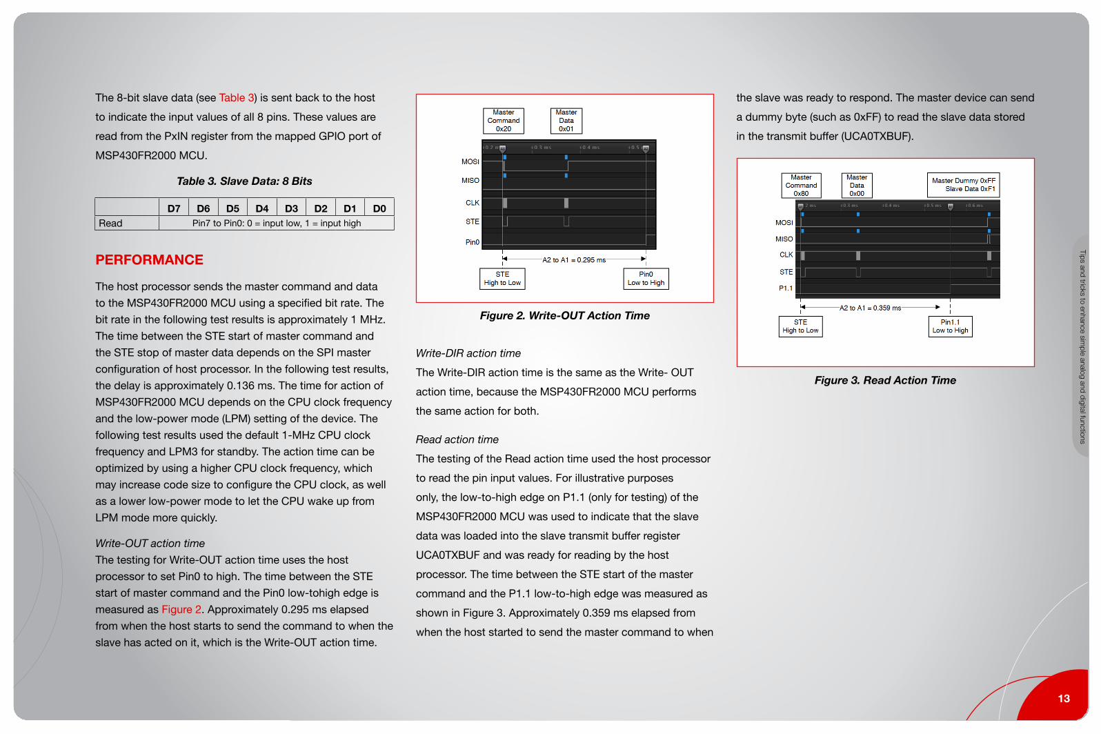
The solution uses an MSP430FR2000 MCU and an external
RGB LED with a current limiting resistor and P-FET for each
of the three LED colors . This allows the LED to be controlled
by the MSP430™ MCU, but driven by more current than
should be supplied directly from an MSP430 device output
pin . The LED BoosterPack™ plug-in module used comes
from the TIDM-G2XXSWRGBLED TI Design – schematics
and additional information can be found there . The
MSP430FR2000 MCU was used with the MSPTS430PW20
target socket board and connected with wires to the
BoosterPack module as shown in Figure 1 . The backchannel
UART of the MSP-FET programmer and debugger or eZ-FET
on an MSP430™ LaunchPad™ development kit was used
for the UART communication with a terminal program on the
PC to send the commands for selecting each color .
Figure 1. RGB LED Controller Block Diagram
The theory of RGB color mixing using PWMs is further
elaborated on in the MSP430 Software RGB LED Control
Design Guide Section 3 .1, RGB Color Mixing, and Section
3 .2, LED Control . However, to save code space a different
methodology is used to create the PWMs . The PWMs
are controlled by the TB0CCR0 (Blue), TB0CCR1 (Red),
and TB0CCR2 (Green) registers in the Timer B0 module .
Typically, when generating PWMs with the timer module the
timer is used in Up Mode and TB0CCR0 sets the period .
With that method only (Number of CCRs – 1) PWMs can
be generated on a single timer module – with the Timer B0
with 3 CCRs on the MSP430FR2000 device, only 2 PWMs
would be possible . Therefore, a different method is used to
create the PWMs using continuous mode . The theory behind
this hardware timer plus software ISR handling approach
is explained further in Multiple Time Bases on a Single
MSP430 Timer Module .
Because the frequency only needs to be approximately 60
Hz to prevent visible flicker, the master clock (MCLK) can
remain at the default 1 .048 MHz without running into the
limitations presented in Multiple Time Bases on a Single
MSP430 Timer Module . The PWMs are generated from the
auxiliary clock (ACLK) sourced from the internal trimmed
low-frequency reference oscillator (REFO) at 32768 Hz . The
clock is divided by 4 to produce 8192 Hz as the timer clock
– this makes it so that the period of 60 Hz can be generated
with TB0CCRx values totaling 135 for the period value .
Because 135 is less than 255 (FFh) the lookup tables for the
timer periods for different RGB values can be made up of
8- bit values, saving additional program memory space on
UART Software Controlled RGB LED Color Mixing With MSP430™ MCUs
15
Tips and tricks to enhance simple analog and digital functions
small devices . Note that the LEDs are turned on during the
low phase of the PWM, so colorsLow[] contains the values
for the LED on period and colorsHigh[] contains the values
for the LED off period .
PERFORMANCE
To run the demo, connect the hardware as previously
described, load the code into the device, allow the
device to run and end the debug session . Note that
the MSP-TS430PW20 target board already includes
the correct connections for the UART TXD and RXD
on the MSP-FET connector as long as JP14 and JP15
are populated (leave JP13 unconnected) . At startup,
the LED will appear white as the device initialization
occurs (because the P-FETs controlling the LED are
active low) . Once the initialization is complete the LED
will default to red . Using the backchannel UART on the
MSP-FET or the eZ-FET, use a terminal program on
the PC set to 9600 baud none parity 1 stop bit to
select the colors . There are 12 colors, selectable by
sending a single hex byte of 0 to Bh . Any invalid value
defaults to red .
Figure 2. Write-OUT Action Time
The demo produces 12 colors tuned to the LED on the
BoosterPack module . If a larger MSP430 MCU were used,
then many more colors could be added . For this RGB LED,
the red LED has a lower intensity than the green or blue
LEDs . Therefore, the values in colorsHigh[] and colorsLow[]
were tuned to have less green and blue when mixing with
red to produce the desired colors . For best viewing, use
a diffuser so that the three LEDs can fully blend into the
resultant color . This solution provides RGB LED control with
minimal external components and optimized software that
fits in code-limited devices down to 0 .5KB .

Texa
s In
stru
men
ts
16
INTRODUCTION
Used in several industrial applications such as robotics,
factory automation, and device positioning, servo
motors allow for precise control of either angular or
linear positioning and as such have become necessary
components of several sophisticated systems . By
integrating a motor, driver, encoder, and electronics into a
single unit, the motor can be controlled by a microcontroller
(MCU) using Pulse Width Modulation (PWM) signals . This
modulation technique varies the duty cycle of a known
frequency which correlates with the motors position .
Typically, this is provided in the form of 1- to 2-ms pulses
of a 20-ms waveform (or 50 Hz at 5% to 10% duty cycle)
for a total 180˚ of motor movement . See Figure 1 for further
signal conditioning and device connection details, but note
that these can differ based on the motor used and, as such,
always consult the data sheet of the servo .
Figure 1. Servo Motor Connections and Waveform
The example code included with this documentation
provides basic control of a servo motor though UART
hexadecimal commands to a MSP430FR2000 device . This
MCU provides a cost-effective solution, which is achieved
while keeping the code size below the available 512 bytes of
main memory . To get started, download project files and a
code example demonstrating this functionality .
IMPLEMENTATION
MSP430™ device GPIO pins allow for a maximum output
of 3 .6 V, depending on its VCC level . However, most servo
motors operate on a 5-V rail and therefore require some form
of voltage level translation to be driven by the microcontroller .
It is possible to use an N-channel MOSFET as a logic
switch, as shown in Figure 2 with the CSD18537NKCS, or
a unidirectional voltage translation device (such as from the
SN74LV1Txx family) to accomplish this task .
Figure 2. Servo Motor Circuit Diagram
PWM signals can be generated through the use of a timer
peripheral, in this case Timer_B0 . The default ACLK supply
from internal trimmed low-frequency reference oscillator
(REFO) (approximately 32 kHz) is used to source the timer,
which operates in up mode . The TB0CCR0 register is set to
produce a 20-ms period . Likewise, the TB0CCR1 register
establishes the duty cycle, or amount of time during the
period for which a signal is driven high, and controls the
output to the P2 .0/CCR1 pin of the MSP430FR2000 MCU .
The duty cycle should remain between 1 and 2 ms to
effectively control the servo motor .
In this example, a terminal program is used to provide a
straightforward method for controlling servo motor position .
The eUSCI_A0 peripheral is used in UART mode, enabling
commands to be received on P1 .6/UCA0RXD . An MSP-FET
programmer and debugger and a MSP-TS430PW20 target
development board is used for evaluation . A baud rate of
4800 must be selected with one stop bit and no parity . A
hexadecimal input from 0x00 to 0x0F selects the motor
position, from its starting position to the maximum rotation
allowed, in incremental steps . CCR1 register values are
determined through the use of a lookup table (see Table 1),
which provides the predefined duty cycle value .
Servo Motor Controller Using MSP430™ MCUs

17
Tips and tricks to enhance simple analog and digital functions
Table 1. Hex to Duty Cycle Lookup
Received Byte TB0CCR1 Value Output Duty cycle
0x00 33 1 .00 ms (5 .0%)
0x01 36 1 .10 ms (5 .5%)
0x02 38 1 .16 ms (5 .8%)
0x03 40 1 .22 ms (6 .1%)
0x04 42 1 .28 ms (6 .4%)
0x05 44 1 .34 ms (6 .7%)
0x06 46 1 .41 ms (7 .1%)
0x07 48 1 .46 ms (7 .3%)
0x08 50 1 .53 ms (7 .7%)
0x09 52 1 .59 ms (8 .0%)
0x0A 54 1 .65 ms (8 .3%)
0x0B 56 1 .71 ms (8 .6%)
0x0C 58 1 .77 ms (8 .9%)
0x0D 60 1 .83 ms (9 .2%)
0x0E 62 1 .89 ms (9 .5%)
0x0F 65 1 .98 ms (9 .9%)
PERFORMANCE
Figure 3 shows three examples of PWM waveforms
generated from hexadecimal terminal entries (in red) . The
1-ms pulse refers to 0˚ rotation of the servo motor, whereas
a 2-ms pulse turns the motor to 180˚ . 1 .5 ms therefore sets
the position near 90˚, and so forth .
Figure 3. Duty Cycle Modulation
The code example uses approximately 200 bytes of main
memory . This leaves more space for additional application
code, detailed position sequences, or dual servo motor
control by employing the TB0CCR2 register on P2 .1 .
MSP430 MCUs with larger memory footprints can be
substituted to further increase functionality . If the eUSCI
peripheral is not required then PWM outputs can also be
accessed through the P1 .6 and P1 .7 pins .
A FRAM variable is used to save the position of the servo
motor . In instances where the device is reset, for example by
pulling the RST line low or through an unintentional power
cycle, then CCR1 retains the duty cycle output necessary to
keep the servo motor in its former position . This functionality
can be removed or disabled if the application does not
require the motor to reposition itself any time a reset occurs .
Although REFO supplies a 32-kHz frequency to ACLK for
the UART baud-rate source, an external crystal can be
substituted as it is more stable over temperature changes .
During inactivity, the code utilizes low-power mode 3 (LPM3)
to achieve power consumption currents of 17 μA as realized
through LPM3, but using a LFXT instead reduces this power
consumption to 1 μA .

Texa
s In
stru
men
ts
18
INTRODUCTION
Stepper motors are a form of brushless DC electric motor
that convert input pulses into specifically defined increments
as each pulse creates rotation toward a fixed angle . By
dividing full rotation into equal steps, the motor’s position
can then be controlled with advanced precision . Offering
several advantages including high reliability, excellent
response times, and a wide range of torque and speed
options, stepper motors are used in consumer electronics,
industrial systems, and factory automation .
Stepper motor drivers, such as the DRV8825 used for
the purposes of this document, employ a simple step
and direction interface to allow easy interfacing to
microcontrollers (MCUs) . By simply adjusting a timer pulse
width modulation (PWM) output frequency and incorporating
an additional general-purpose output pin, it is possible for
a MSP430™ MCU to regulate the speed and direction at
which a stepper motor is driven . Commands are also simple
enough such that a stepper motor can be controlled by the
MSP430FR2000 MCU, a cost-effective MCU with 512 bytes
of main memory . To get started, download project files and a
code example demonstrating this functionality .
IMPLEMENTATION
The DRV8825 manages all protection features necessary
when interfacing with a brushless DC motor, and therefore,
all that is required from the MSP430 device are the step,
direction, and ground connections . The RESET and SLEEP
pins are pulled high, because they do not need to be directly
controlled, and the M2 pin is also pulled high so that 1/16th
microstepping mode is used . Operating supply voltage
ranges, maximum drive currents, timing requirements, and
allowed modes vary between stepper motor drivers, so see
the device-specific data sheet . A DRV8825-based breakout
board is used for the purpose of this demonstration,
and Figure 1 shows the connections for this board . The
DRV8886AT is a suitable alternative that includes updated
features like autotune and internal current sensing .
Figure 1. Stepper Motor Circuit Diagram
Timer_B0 is used to generate the PWM output to the
DRV8825 STEP pin through P2 .0 . MCLK is initialized at
16 MHz then divided by two to avoid ferroelectric random
access memory (FRAM) wait states, The resulting 8-MHz
frequency shared with SMCLK is used to source the timer
operating in up mode . TB0CCR0, which controls the
output frequency, varies depending on the desired stepper
motor speed . TB0CCR1 maintains a 50% duty cycle as is
expected by the DRV8825 .
A UART host interface must connect to P1 .6/UCA0RXD
to send commands to the eUSCI_A0 peripheral of the
MSP430FR2000 device . An MSPFET programmer and
debugger and MSPTS430PW20 target development board
are used for evaluation . A baud rate of 9600 with one stop
bit and no parity is provided as the default . However, this
can be easily altered to meet application requirements . A
hexadecimal input value of 0x00 stops the motor movement .
An input value of 0x0A inverses the polarity of the P2 .1
output connected to the DIR pin, which causes the motor to
change direction . Other values from 0x01 to 0x09 change
the motor speed from slowest to fastest, respectively . Valid
frequency and timing requirements depend on the specific
stepper motor driver being used . Table 1 lists the default
frequencies used in the example .
Stepper Motor Control Using MSP430™ MCUs

19
Tips and tricks to enhance simple analog and digital functions
Table 1. Hexadecimal to Frequency Mapping
Received TB0CCR0 Frequency (kHz)
0x00 0 0
0x01 8000 1
0x02 4000 2
0x03 2000 4
0x04 1000 8
0x05 500 16
0x06 250 32
0x07 125 64
0x08 64 125
0x09 32 250
PERFORMANCE
Figure 2 shows three examples of PWM waveforms
generated from hexadecimal terminal entries (in red),
validating the entries provided in Table 1 . Faster entries were
not tested with a physical stepper motor setup, as it w as
limited by the power supply’s maximum current draw .
Figure 2. Frequency Modulation
The code example uses approximately 250 bytes of main
memory . This leaves more space for additional application
code, detailed movement sequences, or dual motor control
through P2 .1/CCR2 . An increase in code development might
require migrating to MSP430 MCUs with larger memory
footprints . If the eUSCI MSP430 is a trademark of Texas
Instruments . All other trademarks are the property of their
respective owners . peripheral is not required, more timer
outputs can be generated through the P1 .6 and P1 .7 pins .
However, one timer (Timer_B0) and two capture/compare
registers (CCR1 and CCR2) limit the number of distinct
frequencies that can be generated at any time .
Because the subsystem master clock (SMCLK) is required
as the timer clock source, low-power mode 0 (LPM0) can
be accessed during inactivity and consumes 300 μA on
average . If only using frequencies of 8 kHz or below, then
auxiliary clock (ACLK) can supply the timer instead, and
LPM3 mode can be used to achieve power consumption of
1 μA (LFXT) or 17 μA (REFO) .

Texa
s In
stru
men
ts
20
INTRODUCTION
Many applications, such as toys, musical tuners, function
generators, and others require the generation of reference
analog waveforms and signals . This is often done using
a digital-to-analog converter, however with a few passive
components, this can be achieved by utilizing pulse width
modulation (PWM) signals . This report demonstrates how
to generate time-variant and DC signals; however, it can
be adapted to construct many other arbitrary signals using
tables or counters, multiple programmable DC levels,
or a combination . For supplemental reading, see Using
PWM Timer_B as a DAC Microcontrollers . To get started,
download project files and a code example demonstrating
this functionality .
This example realizes an 8-bit DAC generating a 250-Hz
sine wave, oversampled at 16x, and a DC signal . The sine
wave is achieved by storing the sine samples in a lookup
table, and updating the PWM duty cycle duration with the
next sample after each PWM cycle . The PWM is output
to an RC filter, which removes the higher-frequency signal
components and reconstructs the sine wave . For this
reason, it is best for the PWM frequency to be much higher
than the desired sine frequency . To generate the DC, a
constant duty cycle is maintained .
The target device, the MSP430F R2000 MCU, is a cost-
effective device with 512 bytes of main memory . Larger
MSP430™ devices can be substituted for more data storage
or added functionality .
Figure 1. PWMs and Output
In Figure 1, the sine PWM duty cycle can be seen changing
after each PWM period, whereas the DC duty cycle is not . The
sine and DC waves are seen at the output of the RC filters .
IMPLEMENTATION
The resolution of the DAC is determined by the timer count
length (28 = 256) . The sampling rate, or PWM frequency, can
be found by multiplying the sine frequency by the number of
samples per sine cycle, which gives 8 kHz .
32Samples × 250 Hz = 8 kHz (1)
An easy way to think about this relationship is that the
capacitor is essentially averaging the output samples over
time . So the sampling rate is the output sample speed
required to construct a 250Hz periodic signal with 32
samples per cycle .
The PWM clock frequency is then found by multiplying the
sampling frequency by the number of timer counts, which
gives 2 .048 MHz . To achieve this, the digitally controlled
oscillator (DCO) has been set to 16 MHz, with a master
clock (MCLK) divider of 4, and a subsystem master clock
(SMCLK) divider of 2, (16 MHz / 4 / 2 = 2 MHz) . SMCLK then
sources Timer_B, which has CCR0 = 256 .
Dual-Output 8-Bit PWM DAC Using Low-Memory MSP430™ MCUs

21
Tips and tricks to enhance simple analog and digital functions
Resolution, PWM frequency, and PWM clock frequency can
also be shown in the relation:
fclock= fPWM × 2nBits
where: nBits = the bit resolution of the DAC (2)
The CCR0 interrupt is enabled and, each time it fires, the
ISR updates the PWM duty cycle, stored in CCR1 . This is
done by incrementing the counter variable to point within
a 32-element sine wave array . CCR2 is loaded with a
constant PWM duty cycle to generate the DC signal . CCR1
and CCR2 are configured for pins P1 .6/TB0 .1 and P1 .7/
TB0 .2 . Alternatively, P2 .0 and P2 .1 could be used . Both
CCR output modes are set to reset/set . In this mode, each
output is reset when the counter reaches the respective
CCRx value and is set when the counter reaches the CCR0
value . This provides positive pulses equivalent to the value
in CCRx on each respective output .
By outputting the sine PWM to a 2-pole stacked RC filter,
the sine wave is reconstructed and the PWM switching
is filtered out . The R and C values can be determined by
Equation 3 .
fc= 1
where: R1C1 = R2C2 = RC (3)
The filter cutoff (here 795 Hz) is chosen to be sufficiently
higher than the bandwidth edge to reduce attenuation, but
lower than the frequency of the PWM signal to filter out its
switching . This filter gives better response when R2>>R1,
due to the effect of the voltage divider that is present .
The second order passive filter topology was chosen for
its simplicity, however necessitates a higher sampling
frequency than if a higher order filter was used .
The filter for the DC signal is simply used for charge storage;
thus, a single-pole filter is implemented .
This solution uses an MSP430FR2000 MCU and external
resistors and capacitors to build the RC filter . The
MSP430FR2000 device was used with the MSPTS430PW20
target development board and connected as shown in
Figure 2 .
Figure 2. Output Filter Diagram
PERFORMANCE
To run the demo, connect the hardware as previously
described, load the code into the device, allow the device
to run and end the debug session . Connect P1 .6, P1 .7, and
the filter outputs to an oscilloscope or analog-capable logic
analyzer to observe the signals (see Figure 3) .
Figure 3. C2 = 220 pF, 1.64 VDC, 50% PWM
2πRC

Texa
s In
stru
men
ts
22
The output can be cleaned up by increasing the order of the
filter, where the attenuation at the cutoff point of an nth-order
filter can be found by Equation 4 .
(4)
or, by tuning the cutoff point further away from the PWM
frequency, achieved here by increasing C2 to 420 pF (see
Figure 4) . However, the criterion for the previous fC relation
is violated; therefore the frequency (549 Hz in this example)
is now obtained by Equation 5 .
fc= (5)
Additionally, the DC level can be changed by adjusting
the duty cycle of the DC PWM (see Figure 3 and Figure 4) .
These values are directly proportional (attenuation may need
to be accounted for depending on filter design) and follow
the relationship:
where: D = PWM duty cycle (6)
Figure 4. C2 = 420 pF, 3.32 VDC, 100% PWM
Furthermore, the DC and time-variant signals can be
summed using a summing amplifier to achieve an offset .
A simple up or up-down counter can be implemented to
generate a ramp or triangle wave (see code and Figure 5) .
These topics are covered further in Using PWM Timer_B as
a DAC Microcontrollers; however, the ISR to achieve a ramp
and the resulting waveform are included below .
/** * TimerB0 Interrupt Service Routine **/#pragma vector=TIMER0_B0_VECTOR__interrupt void TIMER0_B0_ISR( void){
//Increment PWM duty cycle in steps of 8//To adjust frequency, change step sizedutyCycle+=8;// Set CCR1 using a 256 count bit maskTB0CCR1 = dutyCycle & 0x0FF;
}
Figure 5. Output Ramp (Top Zoomed)
Presumably, many other arbitrary waveforms can be
reconstructed using the methods above, provided an
oversampled table of the signal has been constructed . If the
sample table exceeds 500 bytes, other MSP430 MCUs are
available with larger memory sizes .
VDC = D x VCC
Vout
Vin = √2
1( )n
√1
R1C1R2C2

23
Tips and tricks to enhance simple analog and digital functions
MSP-EXP430FR2433
LaunchPad Development Kit
Features:
• Ultra-low-power MSP430FR2433 16-bit MCU with 16KB FRAM
• 8 channel 10-bit ADC
• 32 x 32 multiplier
• EnergyTrace++ Technology available for ultra-low-power debugging
• 20-pin LaunchPad kit standard leveraging the BoosterPack ecosystem
• On-board eZ-FET debug probe
• 2 buttons and 2 LEDs for user interaction
Learn more
Texa
s In
stru
men
ts
24
INTRODUCTION
An analog-to-digital converter (ADC) is a system that
converts an analog signal, such as analog voltage or
current to a digital number proportional to the magnitude
of the voltage or current . In some applications such as
lighting or DC electric motor control, the output will be a
pulse width modulation (PWM) signal . The MSP430FR2000
microcontroller (MCU) does not include an ADC module . In
this example, the enhanced comparator (eCOMP) is used to
implement a 6-bit ADC function .
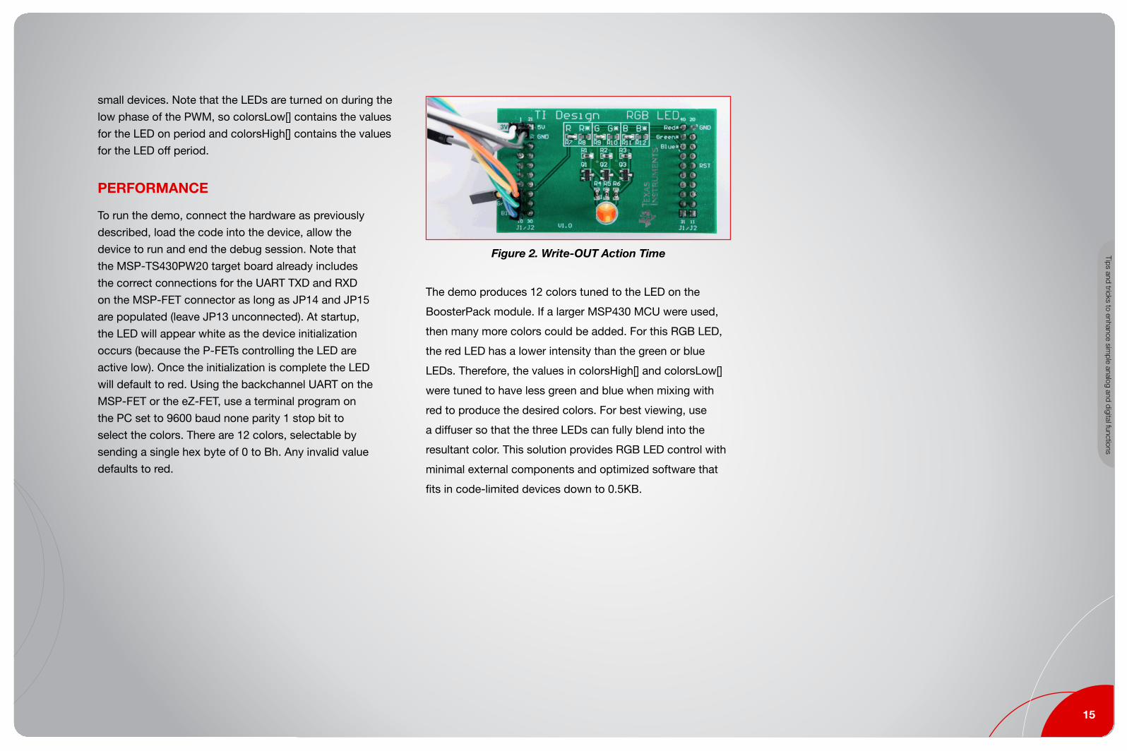
The implementation presented here demonstrates how
to use the MSP430™ on-chip analog voltage comparator
with an internal reference digital-to-analog converter
(DAC) to measure the voltage then output PWM signals .
This has been optimized for lowest code size, fitting in
MSP430FR2000 MCU, which contains 512 bytes of main
memory . To get started, download project files and a code
example demonstrating this functionality .
IMPLEMENTATION
The eCOMP module compares the analog voltages at
the positive (V+) and negative (V–) input terminals . In this
solution the external voltage is connected to the positive
input terminal and the eCOMP’s built-in 6-bit DAC is
connected to the negative terminal .
A GPIO (P1 .3) interrupt is used for mechanical button input
detection . This is used to trigger an ADC conversion and
output a PWM signal from the MSP430FR2000 device
output pin . A capacitor is connected to P1 .3 for debouncing .
The MSP430FR2000 was used with the MSP-TS430PW20
target development board and connected with wires to the
mechanical buttons and voltage input as shown in Figure 1 .
Figure 1. eCOMP ADC And PWM Output Block Diagram
This demo uses the on-chip 1 .5-V VREF as the reference
voltage for the DAC . The input voltage is measured by
finding the correct setting for CPDACDATA . The buffer data
is initialized as 0x20 which is 32 of 64 steps . If the result
of the compare is positive then the buffer data needs to
be increased and compared again . If the result is negative
then the buffer data needs to be decreased and compared
again . With this iterative process the correct buffer data
value should be found after several iterations . The buffer
data value is then used to generate different PWM signals
to indicate the input voltage . Timer_B0 is used to generate
the PWM output on P2 .0, and the PWM frequency and duty
cycle are set by TB0CCR0 and TB0CCR1 .
To run the demo, connect the hardware as previously
described, load the code into the device, allow the device
to run and end the debug session . Note that the MSP-
TS430PW20 target board already includes the correct
connections for the MSP-FET programmer and debugger . At
startup, connect Vinput to the external voltage that needs to
be measured . Pressing the button will start the measurement
and output the PWM .
Analog Input to PWM Output Using the MSP430™ MCU Enhanced Comparator
25
Tips and tricks to enhance simple analog and digital functions
The 6-bit DAC can be set to 64 levels, which gives an effective
resolution for this ADC of 6 bits . In the example code, the
expected PWM frequency can be translated from Vinput .
fpwm = 1 / (Buffer Data × 128) (1)
The duty cycle is always 50% . The frequency and duty cycle
could be changed based on application requirements . Table 1
lists some PWM frequency examples with the Vinput .
Table 1. Voltage to PWM
Vinput (V) Buffer Data Frequency (kHz)
0 1 8000
0 .5 23 340
1 43 181
1 .5 63 124
PERFORMANCE
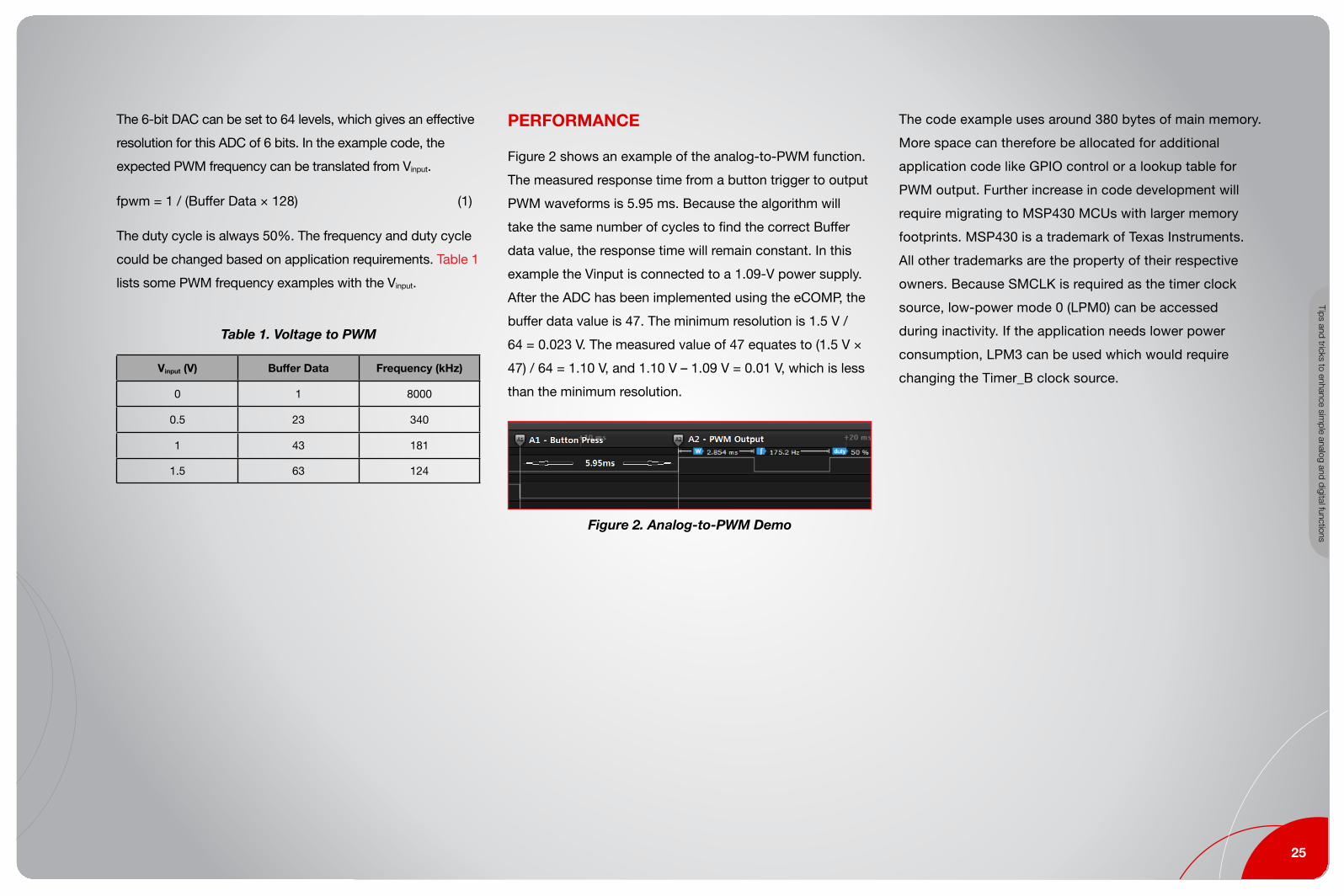
Figure 2 shows an example of the analog-to-PWM function .
The measured response time from a button trigger to output
PWM waveforms is 5 .95 ms . Because the algorithm will
take the same number of cycles to find the correct Buffer
data value, the response time will remain constant . In this
example the Vinput is connected to a 1 .09-V power supply .
After the ADC has been implemented using the eCOMP, the
buffer data value is 47 . The minimum resolution is 1 .5 V /
64 = 0 .023 V . The measured value of 47 equates to (1 .5 V ×
47) / 64 = 1 .10 V, and 1 .10 V – 1 .09 V = 0 .01 V, which is less
than the minimum resolution .
Figure 2. Analog-to-PWM Demo
The code example uses around 380 bytes of main memory .
More space can therefore be allocated for additional
application code like GPIO control or a lookup table for
PWM output . Further increase in code development will
require migrating to MSP430 MCUs with larger memory
footprints . MSP430 is a trademark of Texas Instruments .
All other trademarks are the property of their respective
owners . Because SMCLK is required as the timer clock
source, low-power mode 0 (LPM0) can be accessed
during inactivity . If the application needs lower power
consumption, LPM3 can be used which would require
changing the Timer_B clock source .

Texa
s In
stru
men
ts
26
INTRODUCTION
Electrically Erasable Programmable Read-Only Memory
(EEPROM) devices are often used by end applications to
store relatively small amounts of data which are retained
when power is not supplied to the system . This type of
data storage is valuable to applications requiring calibration
data, unit identification, or backup information . Such an
operation can be emulated by using ferroelectric random
access memory (FRAM) available on select MSP430™
microcontrollers (MCUs) . The ultra-lowpower nature of
FRAM makes it a great option for EEPROM emulation
enabling nonvolatile writes for a fraction of the power used
by conventional memories . Furthermore, FRAM offers
practically unlimited write cycles and is not stressed from
constantly logging data or saving system information . 48
bytes of FRAM are allocated to EEPROM functionality on the
MSP430FR2000 MCU, a cost-effective FRAM device that
has only 512 bytes of main memory, but larger devices can
be substituted for more data storage or added functionality .
To get started, download project files and a code example
demonstrating this functionality .
IMPLEMENTATIOM
EEPROM emulation is configured to use SPI protocol in
slave mode . A host processor acting as the master should
be connected so that it can write or read data from the
MSP430 MCU . Beyond the typical SPI bus (SCLK, MOSI,
MISO, and CS) a write protect (WP) line is also used . Figure 1
shows the SPI block diagram interface .
Figure 1. EEPROM SPI Block Diagram
The CS pin determines if the SPI is enabled and is active low
by default . Communication is achieved by sending an op
code followed by an 8-bit address, after which the EEPROM
can be written to or read from until the memory space
allocation has been exceeded or the CS line resets the SPI .
The two op-code values are 0x02 (write) and 0x03 (read) but
can be changed to the user’s preference . Up to 256 bytes
of EEPROM memory can be utilized on FRAM devices that
exceed 512 bytes of total memory, but additional space
will require changes to the code, because it accounts for
only 8-bit addressing . The EEPROM page is protected from
write commands until the WP line is driven low but read
commands can be performed at any time . Figure 2 and
Figure 3 show an interface example between a host device
and MSP430 FRAM EEPROM emulator, in which a word is
written starting at 0x0F and then read from 0x10 .
Figure 2. EEPROM Write Word Sequence
EEPROM Emulation Using Low-Memory MSP430™ FRAM MCUs

27
Tips and tricks to enhance simple analog and digital functions
Figure 3. EEPROM Read Word Sequence
As seen in Figure 2, the “write” op-code (0x02) is followed
by the desired address (0x0F), after which the word 0xCEB4
is supplied . A “read” op code (0x03) quickly follows with
the address 0x10, and the MSP430 MCU responds with the
0xB4 value that was previously given as well as the preset
value (0x11) stored at the memory address 0x11 . Further
investigation reveals that 0xCE has been properly written
to address 0x0F as well . After the op code and address
are given, writes or reads can continue repeatedly until the
end of the memory page has been reached, at which point
further instructions are ignored .
PERFORMANCE
Using the MSP430FR2000 MCU has certain restrictions due
to the 0 .5KB of memory . For example, Figure 3 shows that a
75 μs delay is required between the high-to-low transition of
the CS/EN pin and the start of the system clock (SCLK) . 150
μs must also pass between the read address and reading
from the EEPROM memory, and the CS/EN pin must remain
high for at least 100 μs between SPI sequences .
Upgrading to one kilobyte of memory with the
MSP430FR2100 MCU or reducing the necessary EEPROM
page size allows enough additional memory space for
increasing the operating frequency for faster response
times . For a fuller featured and larger EEPROM memory,
other MSP430 FRAM MCUs can be used with the TIDM-
FRAM-EEPROM reference design, which uses the 256KB
MSP430FR5994 device .
The firmware operates in low-power mode 3 (LPM3) when
the SPI is not active but consumes 20 μA of current at 3 V,
some of which is due to the internal pullup resistance on
the CS pin . 15 μA is required to drive the internal trimmed
low-frequency reference oscillator (REFO), but less than
2 μA is achievable by populating an external crystal and
sourcing to the auxiliary clock (ACLK) . Overall current
consumption averages from active SPI communication
depend on the number of bytes written to the FRAM during
each transaction and the frequency to which the EEPROM is
accessed . Use cases therefore need to be further evaluated
by the user .

Texa
s In
stru
men
ts
28
INTRODUCTION
Keypads are used in many applications but implementations
often struggle to achieve a design that is simple, low cost,
and low power . The MSP430FR2000 microcontroller (MCU)
is an ultra-lowpower device that provides a cost-effective
solution using only 512 bytes of nonvolatile ferroelectric
random access memory (FRAM) . The device’s extensive low-
power modes enable extended battery life . A keypad design
utilizing this MCU can implement a completely interrupt-
driven approach that requires no polling and uses minimal
external components . While waiting for a keypress, this
design consumes only 0 .58 μA, and it draws a maximum of
only 2 .6 μA at 3 V if all keys are pressed simultaneously . The
design also takes advantage of the eUSCI peripheral within
the MSP430™ MCU to provide a 4800-baud UART interface
that reports the button pressed to any connected device .
To get started, download project files and a code example
demonstrating this functionality . Additionally, the infrared
BoosterPack™ plug-in module was used to develop and test
this example code with added external pulldown resistors .
IMPLEMENTATION
This keypad design uses the strategy outlined in
Implementing An Ultralow-Power Keypad Interface with
MSP430 MCUs . This approach takes advantage of port 1’s
interrupt capability to wake the device from a low-power
mode . The columns of the keypad are connected to P2 .0,
P2 .1, P2 .6, and P2 .7, and the rows are connected to port
pins P1 .0 to P1 .3 . Figure 1 shows these keypad connections
to the MSP430 MCU and the associated key numbers .
Figure 1. Keypad MSP430 MCU Connections
While the MSP430 device is waiting for a key press, it enters
a wait-for-press mode where the keypad columns are driven
high . Simultaneously the P1 .x rows are configured as inputs
and pulled low using 4 .7-MΩ external pulldown resistors .
The device is then put into low-power mode 4, where the
current consumption is approximately 0 .58 μA, and remains
there until a key is pressed .
When a key is pressed, a physical connection is made
between a column and one of the P1 .x pins . This causes
the P1 .x pin to interrupt on a rising edge and wake the CPU
from low-power mode 4 to continue program execution .
First, the key is debounced using the watchdog timer (WDT)
for an interval of approximately 15 ms . During this time,
the device enters low-power mode 3 to conserve as much
energy as possible .
Upon WDT expiration, the device once again wakes from
low-power mode and performs a key-scanning algorithm
to determine which key is pressed . If a key is pressed,
the MSP430 MCU reports the key number using the
UART interface .
Low-Power Hex Keypad Using MSP430™ MCUs
29
Tips and tricks to enhance simple analog and digital functions
The device then enters a wait-for-release mode where only
one column is driven high . Simultaneously the P1 .x rows are
reconfigured to interrupt on a falling edge associated with
the key being released . This allows the MCU to enter low-
power mode 4 while the key is being held and also limits the
maximum current consumption to the condition in which all
4 keys on a single column are held down .
When the key is released, it is first debounced using the
WDT, and then the key scanning algorithm is executed to
ensure no keys are being held . If any keys remain held,
the wait-for-release mode continues and the device enters
low-power mode 4 . Finally, when all keys are released, the
MSP430 MCU returns to waitfor- press mode .
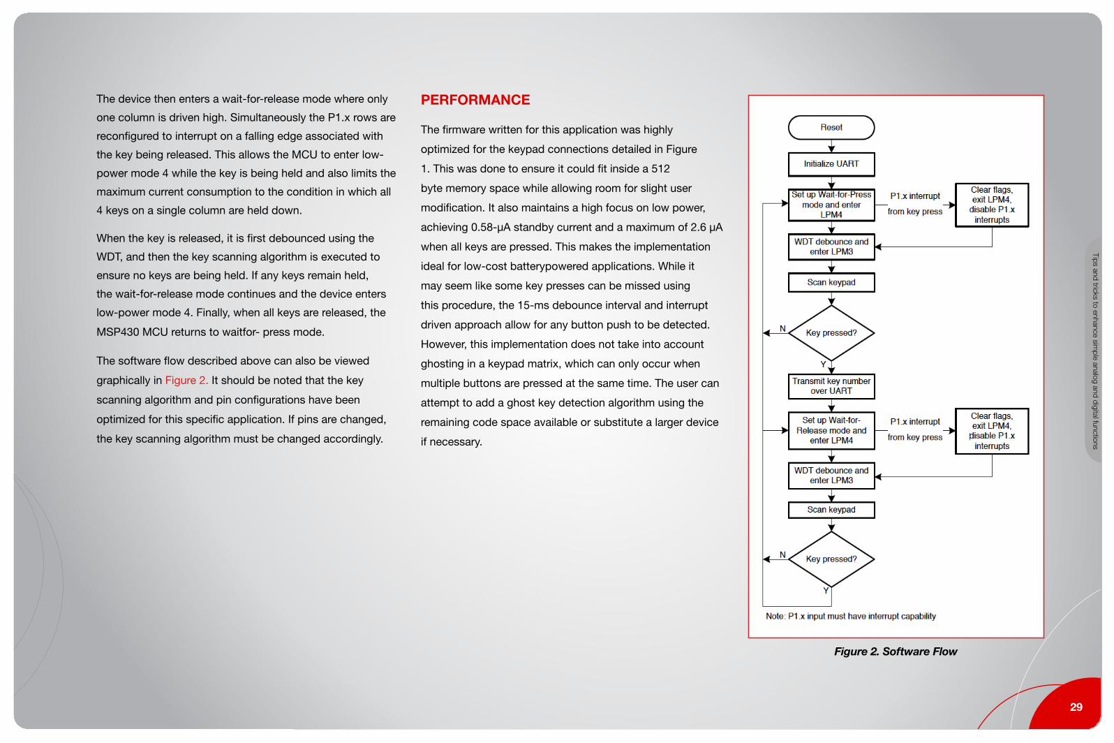
The software flow described above can also be viewed
graphically in Figure 2 . It should be noted that the key
scanning algorithm and pin configurations have been
optimized for this specific application . If pins are changed,
the key scanning algorithm must be changed accordingly .
PERFORMANCE
The firmware written for this application was highly
optimized for the keypad connections detailed in Figure
1 . This was done to ensure it could fit inside a 512
byte memory space while allowing room for slight user
modification . It also maintains a high focus on low power,
achieving 0 .58-μA standby current and a maximum of 2 .6 μA
when all keys are pressed . This makes the implementation
ideal for low-cost batterypowered applications . While it
may seem like some key presses can be missed using
this procedure, the 15-ms debounce interval and interrupt
driven approach allow for any button push to be detected .
However, this implementation does not take into account
ghosting in a keypad matrix, which can only occur when
multiple buttons are pressed at the same time . The user can
attempt to add a ghost key detection algorithm using the
remaining code space available or substitute a larger device
if necessary .
Figure 2. Software Flow
Texa
s In
stru
men
ts
30
INTRODUCTION
Reset controllers are widely used in complex systems in
which the processor is prone to lock-up . The lock-up or
error state can be caused by anything from a software bug
to electromagnetic interference . Using an external reset
controller to do hard or soft reset to the processor can get
the system back to proper state .
The MSP430FR2000 microcontroller (MCU) can be used as
a low-cost solution for reset controller by making use of the
internal Watchdog Timer, interrupt IO, and Timer_B modules .
In this reset controller implementation, a button is used to
initiate a manual reset . A single button or dual buttons can
be detected by an MSP430 MCU in low-power standby
mode . By using the watchdog timer in interval mode, short
and long button presses can be detected . Timer_B using
the internal reference oscillator (REFO) as the clock source
can be used to generate an accurate time delay for the reset
pulse . Button debounce is also implemented in the firmware
to avoid false triggers .
This solution uses the MSP430™ MCU’s low-power mode 4
(LPM4) when not executing a reset operation to save power .
To get started, download project files and a code example
demonstrating this functionality .
IMPLEMENTATION
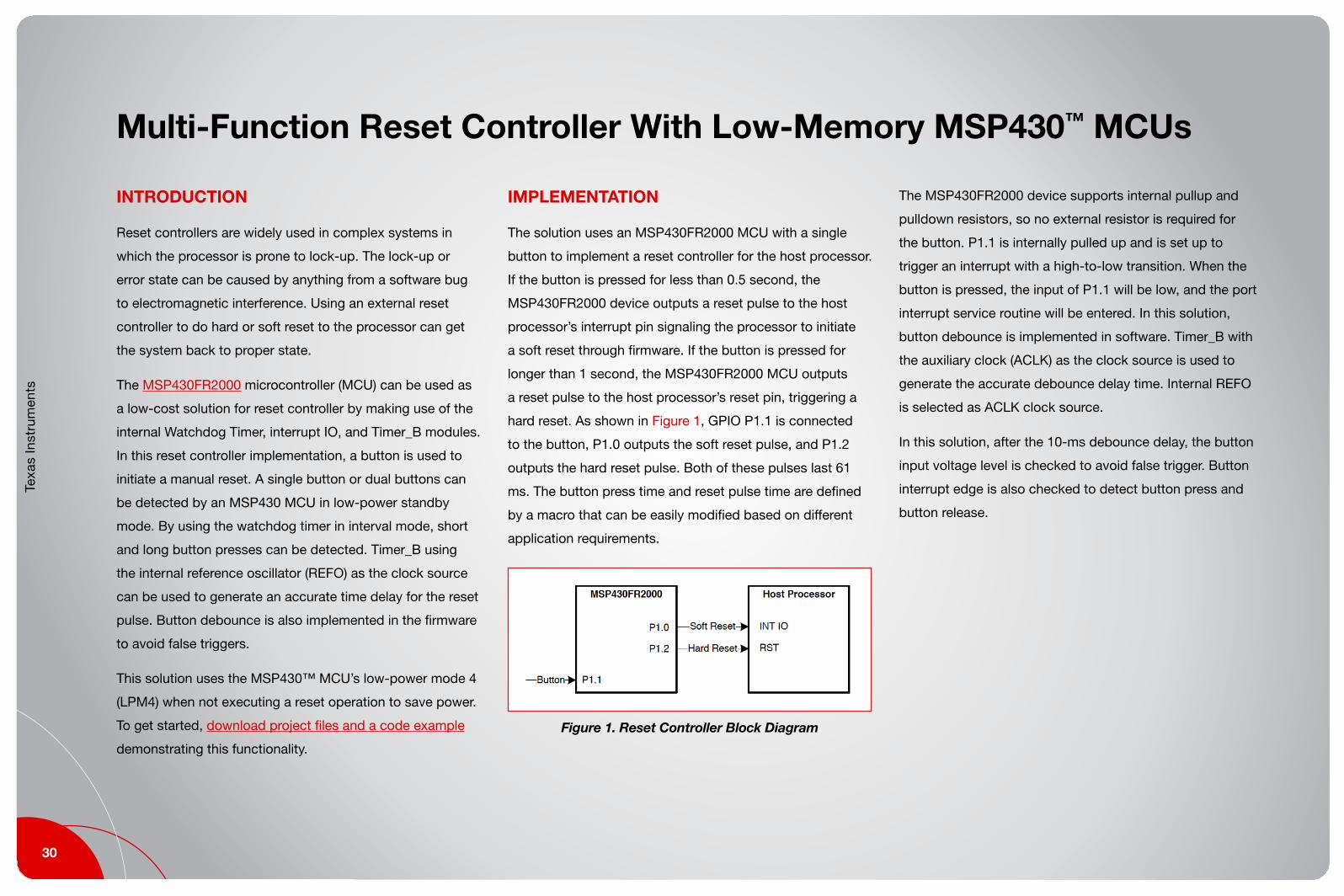
The solution uses an MSP430FR2000 MCU with a single
button to implement a reset controller for the host processor .
If the button is pressed for less than 0 .5 second, the
MSP430FR2000 device outputs a reset pulse to the host
processor’s interrupt pin signaling the processor to initiate
a soft reset through firmware . If the button is pressed for
longer than 1 second, the MSP430FR2000 MCU outputs
a reset pulse to the host processor’s reset pin, triggering a
hard reset . As shown in Figure 1, GPIO P1 .1 is connected
to the button, P1 .0 outputs the soft reset pulse, and P1 .2
outputs the hard reset pulse . Both of these pulses last 61
ms . The button press time and reset pulse time are defined
by a macro that can be easily modified based on different
application requirements .
Figure 1. Reset Controller Block Diagram
The MSP430FR2000 device supports internal pullup and
pulldown resistors, so no external resistor is required for
the button . P1 .1 is internally pulled up and is set up to
trigger an interrupt with a high-to-low transition . When the
button is pressed, the input of P1 .1 will be low, and the port
interrupt service routine will be entered . In this solution,
button debounce is implemented in software . Timer_B with
the auxiliary clock (ACLK) as the clock source is used to
generate the accurate debounce delay time . Internal REFO
is selected as ACLK clock source .
In this solution, after the 10-ms debounce delay, the button
input voltage level is checked to avoid false trigger . Button
interrupt edge is also checked to detect button press and
button release .
Multi-Function Reset Controller With Low-Memory MSP430™ MCUs

31
Tips and tricks to enhance simple analog and digital functions
The MSP430FR2000 MCU goes into LPM4 to wait for an
IO interrupt . When the button is pressed, the MCU wakes
up and starts the watchdog timer to detect the button hold
time . Then the P1 .1 interrupt edge setting is changed from
high-to-low to low-to-high to detect the button release .
The watchdog timer is set to interval timer mode, causing
a watchdog interrupt to be triggered every 250 ms . The
watchdog clock source is also ACLK so that the watchdog
can operate in LPM3 to save power . In the watchdog
interrupt service routine, counter WDT_cnt is used to count
how many times the interrupt is triggered . Based on the
WDT_cnt value, the button press time can be obtained .
When the button is released, if WDT_cnt is smaller than
the short time threshold, a soft reset pulse is generated . If
WDT_cnt is larger than the long time threshold, a hard reset
is triggered . After generating a reset pulse, the MCU enters
LPM4 to wait for next button press . Figure 2 shows the soft
reset pulse where the button is pressed for less than 0 .5
second, and Figure 3 shows the hard reset pulse where the
button is pressed for longer than 1 second .
Figure 2. Soft Reset Pulse (SW_RST)
Figure 3. Hard Reset Pulse (HW_RST)
PERFORMANCE
The MSP430FR2000 MCU was used with the
MSPTS430PW20 target development board to implement this
reset controller solution . The firmware operates in LPM4 when
there is no reset initiated . A standby current consumption of
0 .6 μA was measured using the target development board .
The MCU transitions from standby to active mode, which
only lasts approximately 10 ms, when the button is pressed .
During a long button press, the MCU operates in LPM3 with
approximately 15-μA current consumption .
The reset pulse time is calculated based on REFO clock
with ±3 .5% absolute calibrated tolerance . The minimal
adjustment step size for reset pulse time is one REFO clock
cycle (30 .5 μs) . If higher pulse time accuracy is required,
using the FLL to lock the DCO at high frequency with an
external crystal can achieve higher accuracy with small
time adjustment step size . More performance specifications
can be found in the clock specifications section of the
MSP430FR2100 MCU data sheet .

Texa
s In
stru
men
ts
32
INTRODUCTION
Quadrature encoders are used to keep track of the angular
position of knobs and motors in many applications including
volume control, robotics and factory automation systems .
As a quadrature encoder device rotates, it outputs square
waves on two wires (Line A and Line B), which are tracked by
an interpreter device to determine the device’s position . By
looking at which square wave leads the other, it is possible to
know which direction the device is rotating . If Line B’s square
wave leads Line A’s square wave, the device is rotating
clockwise, and if Line A’s square wave leads Line B’s square
wave, the device is rotating counter-clockwise, as shown in
Figure 1 and Figure 2 . The actual name of the square wave
signals may be different based on the selected quadrature
encoder hardware and manufacturer notation standards .
Figure 1. Quadrature Encoder Clockwise
Rotation Waveforms
Figure 2. Quadrature Encoder Counter-Clockwise
Rotation Waveforms
The values of A and B can be tracked in a state machine
to determine whether the device angle is increasing or
decreasing as shown in Figure 3 . Each time a rising or falling
edge occurs on Line A or B, the device changes states and
the position counter is changed accordingly .
Figure 3. Quadrature Encoder State Machine
The MSP430FR2000 microcontroller (MCU) can hold a
program implementing this state machine to take in the
quadrature encoder input from a device and output the
change in position through UART . Additionally, the internal
real-time clock (RTC) can be used to provide rotational
velocity information by outputting timestamps each time
the position changes . This project has been optimized for
smallest code size and robust handling of human interface
device (HID) inputs . To get started, download project files
and a code example demonstrating this functionality .
Quadrature Encoder Position Counter With MSP430™ MCUs

33
Tips and tricks to enhance simple analog and digital functions
IMPLEMENTATION
This application uses the MSP430FR2000 MCU along with
the MSP-TS430PW20 target development board . As shown
in Figure 4, the MCU pins P1 .1 and P1 .0 are connected to
channels A and B of a quadrature encoder device to track its
position . UART communication occurs on P1 .7 (the MSP-
FET or eZ-FET backchannel UART can be used to connect
to a host processor at 9600 baud to transmit position and
time data) . Note that the MSP-TS430PW20 target board
already includes the correct connections for the UART TXD
and RXD on the MSP-FET connector as long as JP14 and
JP15 are populated (leave JP13 unconnected) .
Figure 4. Hardware Connection Diagram
The firmware implements the state machine shown in
Figure 3 and tracks the change in position of the connected
quadrature encoder device, from the time that the MCU is
powered-on, starting at a value of 0 . The MCU transmits an
unsigned 8-bit integer representing the device’s position,
followed immediately by a 16-bit integer representing the
timestamp through UART each time an edge occurs on Line
A or B as the quadrature encoder hardware is rotated . When
the position counter is at 0 and is decremented, it wraps
around to a value of 255 and vice versa . This number can be
interpreted as a two’s complement number if desired . The
16-bit timestamp is transmitted as two 8-bit integers, with
the high byte transmitted first, and the low byte transmitted
second . Figure 5 shows the data packet structure .
Figure 5. UART TX Data Packet Structure
If only the position data is desired to be transmitted through
UART, the timestamp transmit code in the main while loop
may be commented out as shown in Figure 6 .
Figure 6. Removal of Timestamp Data
The physical angular change can be calculated from the
MCU count using Equation 1 . Units are shown in square
brackets .
∆O [°] = (1)
The angular velocity of the device can be calculated using
the change in the angle, the RTC frequency, and the
difference of consecutive timestamps .
ω [°/s] = (2)
These calculations can be performed in the host processor
program that receives the position and time values through
UART to save code space on the MSP430FR2000 MCU .
PERFORMANCE
The solution uses an MSP430FR2000 MCU and a
quadrature encoder knob . Testing was performed with
the TT Electronics EN11-HSM1AF15 knob, which has 20
positional latch locations, or detents, per revolution .
To run the demo, connect the hardware as previously
described, load the code into the device, allow the device
to run and end the debug session . Using the backchannel
UART on the MSP-FET or the eZ-FET, use a host processor
with UART communication set to 9600 baud none parity 1
stop bit to receive the quadrature encoder knob position and
time data .
(Countnew-Countold) [#]Encoder Resolution [#/°]
∆O [°]*RTC Freq [HzTimestampnew-Timestampold

Texa
s In
stru
men
ts
34
As specified by the knob data sheet, two edges occur on
each of Line A and Line B every time the knob is turned to
a different detent, causing the position counter to change
by four . In many data sheets, the number of detents per
revolution is given as pulses per revolution (ppr), which is
used in the following calculations . The encoder resolution
can then be calculated avs follows:
Encoder Resolution (3)
Encoder Resolution [#/°] = 4 counts per pulse (4)
Encoder Resolution [#/ °]=0 .2222 #/° (5)
The solution configures the RTC to a frequency of 2048 Hz .
The following example demonstrates how to calculate the
angular velocity from real data when the knob is turned from
one detent to the next .
Figure 7. UART Received Position and Time Data
∆O[°] = 2-1 (6)
Time Stampnew=0x1A1F=6687 (7)
Time Stampold=0x19E4=6628 (8)
ω [°/s] = 4 .5°×2048 Hz =156 .2°/s (9)
If Timestampnew–Timestampold is a negative number, 216
(65536) must be added to the value to make it positive . For
the angular velocity calculation to be accurate, the position
counter must change at least once in the time it takes for the
RTC counter to overflow (32 s) .
The firmware can respond to changes in encoder position
at a frequency of at most 200 kHz . Therefore, the maximum
angular velocity that the firmware can track is given by
Equation 10 .
ωmax [°/s] = Interrupt Freq [#/s] (10)
For the knob chosen for testing, the maximum angular
velocity that can be handled by the firmware (150000 RPM)
is well above the maximum hardware operating speed given
in the device data sheet (100 RPM) .
ωmax [°/s] = 200000 #/s = 900000°/s (11)
ωmax = 150000 RPM (12)
∆Count [#]∆O[°]
[#/°] =
360°/ 20 ppr
0 .2222 #/°=4 .5°
6687–6628
Encoder Resolution [#/°]
0 .2222 #/°

35
Tips and tricks to enhance simple analog and digital functions
MSP-EXP430FR4133
LaunchPad Development Kit
Features:
• Ultra-low-power MSP430FR4133 16-bit MCU with 16KB FRAM
• 10 channel 10-bit ADC
• 8 x 32 segment LCD driver with integrated charge pump
• EnergyTrace technology available for ultra-low-power debugging
• 20 pin LaunchPad standard leveraging the BoosterPack ecosystem
• Onboard eZ-FET emulation
• 2 buttons and 2 LEDs for user interaction
• Low-power alphanumeric segmented LCD
Learn more
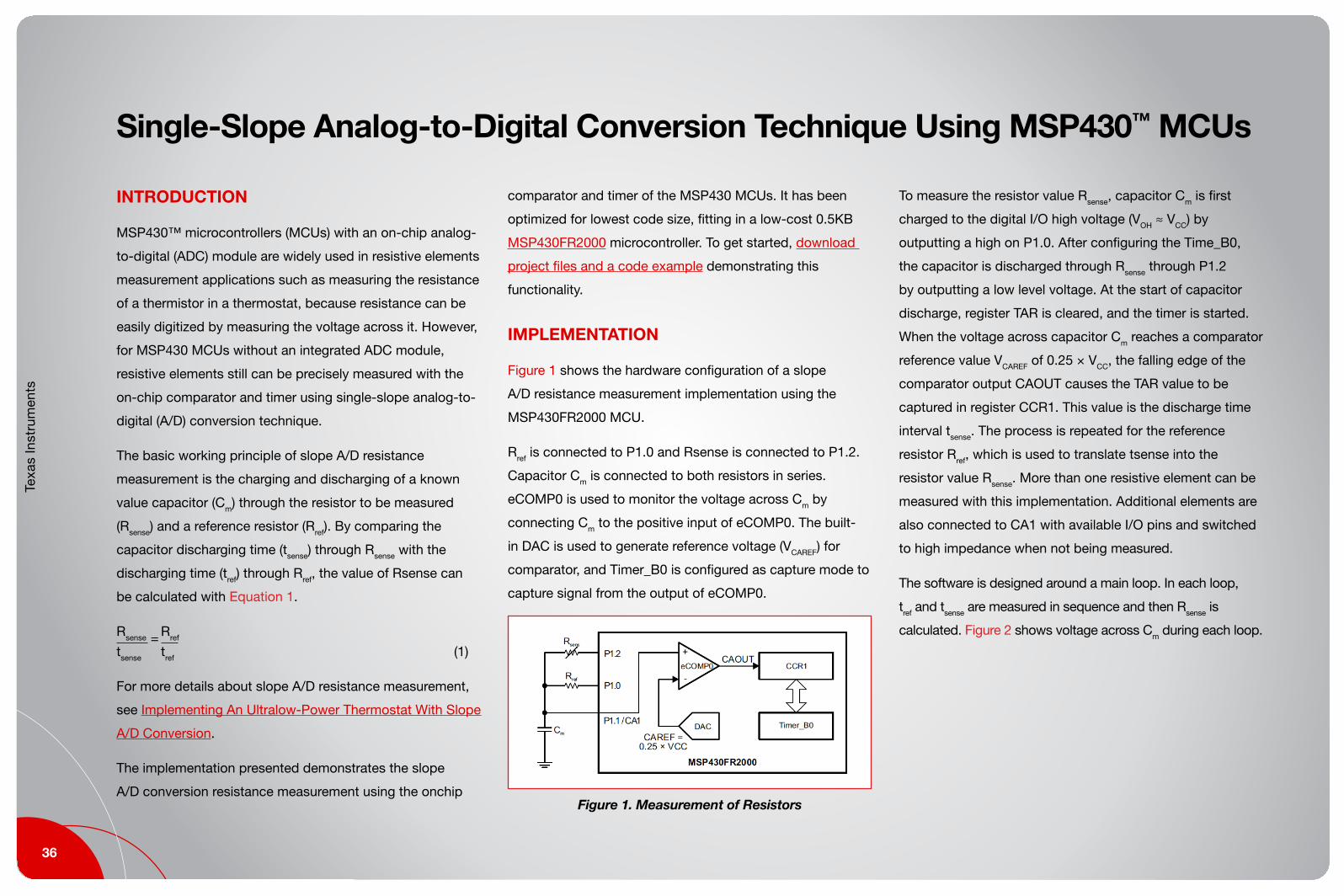
Texa
s In
stru
men
ts
36
INTRODUCTION
MSP430™ microcontrollers (MCUs) with an on-chip analog-
to-digital (ADC) module are widely used in resistive elements
measurement applications such as measuring the resistance
of a thermistor in a thermostat, because resistance can be
easily digitized by measuring the voltage across it . However,
for MSP430 MCUs without an integrated ADC module,
resistive elements still can be precisely measured with the
on-chip comparator and timer using single-slope analog-to-
digital (A/D) conversion technique .
The basic working principle of slope A/D resistance
measurement is the charging and discharging of a known
value capacitor (Cm) through the resistor to be measured
(Rsense) and a reference resistor (Rref) . By comparing the
capacitor discharging time (tsense) through Rsense with the
discharging time (tref) through Rref, the value of Rsense can
be calculated with Equation 1 .
Rsense = Rref
tsense tref (1)
For more details about slope A/D resistance measurement,
see Implementing An Ultralow-Power Thermostat With Slope
A/D Conversion .
The implementation presented demonstrates the slope
A/D conversion resistance measurement using the onchip
comparator and timer of the MSP430 MCUs . It has been
optimized for lowest code size, fitting in a low-cost 0 .5KB
MSP430FR2000 microcontroller . To get started, download
project files and a code example demonstrating this
functionality .
IMPLEMENTATION
Figure 1 shows the hardware configuration of a slope
A/D resistance measurement implementation using the
MSP430FR2000 MCU .
Rref is connected to P1 .0 and Rsense is connected to P1 .2 .
Capacitor Cm is connected to both resistors in series .
eCOMP0 is used to monitor the voltage across Cm by
connecting Cm to the positive input of eCOMP0 . The built-
in DAC is used to generate reference voltage (VCAREF) for
comparator, and Timer_B0 is configured as capture mode to
capture signal from the output of eCOMP0 .
Figure 1. Measurement of Resistors
To measure the resistor value Rsense, capacitor Cm is first
charged to the digital I/O high voltage (VOH ≈ VCC) by
outputting a high on P1 .0 . After configuring the Time_B0,
the capacitor is discharged through Rsense through P1 .2
by outputting a low level voltage . At the start of capacitor
discharge, register TAR is cleared, and the timer is started .
When the voltage across capacitor Cm reaches a comparator
reference value VCAREF of 0 .25 × VCC, the falling edge of the
comparator output CAOUT causes the TAR value to be
captured in register CCR1 . This value is the discharge time
interval tsense . The process is repeated for the reference
resistor Rref, which is used to translate tsense into the
resistor value Rsense . More than one resistive element can be
measured with this implementation . Additional elements are
also connected to CA1 with available I/O pins and switched
to high impedance when not being measured .
The software is designed around a main loop . In each loop,
tref and tsense are measured in sequence and then Rsense is
calculated . Figure 2 shows voltage across Cm during each loop .
Single-Slope Analog-to-Digital Conversion Technique Using MSP430™ MCUs
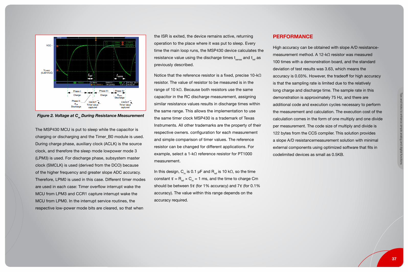
37
Tips and tricks to enhance simple analog and digital functions
Figure 2. Voltage at Cm During Resistance Measurement
The MSP430 MCU is put to sleep while the capacitor is
charging or discharging and the Timer_B0 module is used .
During charge phase, auxiliary clock (ACLK) is the source
clock, and therefore the sleep mode lowpower mode 3
(LPM3) is used . For discharge phase, subsystem master
clock (SMCLK) is used (derived from the DCO) because
of the higher frequency and greater slope ADC accuracy .
Therefore, LPM0 is used in this case . Different timer modes
are used in each case: Timer overflow interrupt wake the
MCU from LPM3 and CCR1 capture interrupt wake the
MCU from LPM0 . In the interrupt service routines, the
respective low-power mode bits are cleared, so that when
the ISR is exited, the device remains active, returning
operation to the place where it was put to sleep . Every
time the main loop runs, the MSP430 device calculates the
resistance value using the discharge times tsense and tref as
previously described .
Notice that the reference resistor is a fixed, precise 10-kΩ
resistor . The value of resistor to be measured is in the
range of 10 kΩ . Because both resistors use the same
capacitor in the RC discharge measurement, assigning
similar resistance values results in discharge times within
the same range . This allows the implementation to use
the same timer clock MSP430 is a trademark of Texas
Instruments . All other trademarks are the property of their
respective owners . configuration for each measurement
and simple comparison of timer values . The reference
resistor can be changed for different applications . For
example, select a 1-kΩ reference resistor for PT1000
measurement .
In this design, Cm is 0 .1 μF and Rref is 10 kΩ, so the time
constant τ = Rref × Cm = 1 ms, and the time to charge Cm
should be between 5τ (for 1% accuracy) and 7τ (for 0 .1%
accuracy) . The value within this range depends on the
accuracy required .
PERFORMANCE
High accuracy can be obtained with slope A/D resistance-
measurement method . A 12-kΩ resistor was measured
100 times with a demonstration board, and the standard
deviation of test results was 3 .63, which means the
accuracy is 0 .03% . However, the tradeoff for high accuracy
is that the sampling rate is limited due to the relatively
long charge and discharge time . The sample rate in this
demonstration is approximately 75 Hz, and there are
additional code and execution cycles necessary to perform
the measurement and calculation . The execution cost of the
calculation comes in the form of one multiply and one divide
per measurement . The code size of multiply and divide is
122 bytes from the CCS compiler . This solution provides
a slope A/D resistancemeasurement solution with minimal
external components using optimized software that fits in
codelimited devices as small as 0 .5KB .
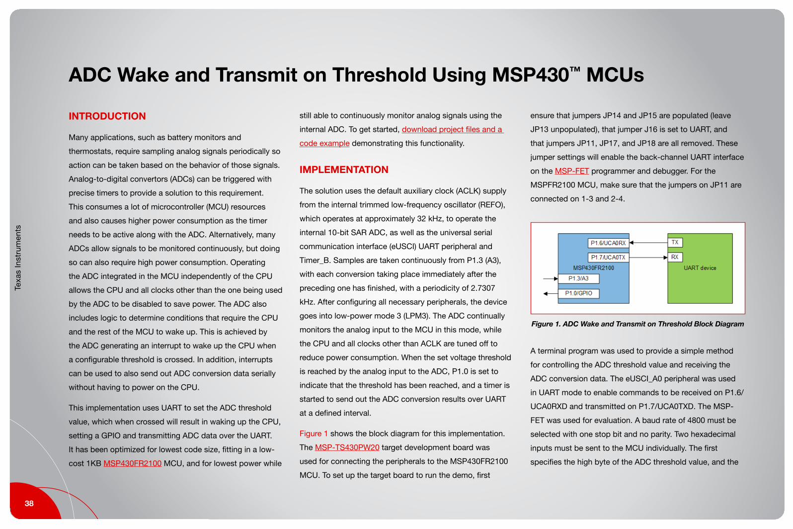
Texa
s In
stru
men
ts
38
INTRODUCTION
Many applications, such as battery monitors and
thermostats, require sampling analog signals periodically so
action can be taken based on the behavior of those signals .
Analog-to-digital convertors (ADCs) can be triggered with
precise timers to provide a solution to this requirement .
This consumes a lot of microcontroller (MCU) resources
and also causes higher power consumption as the timer
needs to be active along with the ADC . Alternatively, many
ADCs allow signals to be monitored continuously, but doing
so can also require high power consumption . Operating
the ADC integrated in the MCU independently of the CPU
allows the CPU and all clocks other than the one being used
by the ADC to be disabled to save power . The ADC also
includes logic to determine conditions that require the CPU
and the rest of the MCU to wake up . This is achieved by
the ADC generating an interrupt to wake up the CPU when
a configurable threshold is crossed . In addition, interrupts
can be used to also send out ADC conversion data serially
without having to power on the CPU .
This implementation uses UART to set the ADC threshold
value, which when crossed will result in waking up the CPU,
setting a GPIO and transmitting ADC data over the UART .
It has been optimized for lowest code size, fitting in a low-
cost 1KB MSP430FR2100 MCU, and for lowest power while
still able to continuously monitor analog signals using the
internal ADC . To get started, download project files and a
code example demonstrating this functionality .
IMPLEMENTATION
The solution uses the default auxiliary clock (ACLK) supply
from the internal trimmed low-frequency oscillator (REFO),
which operates at approximately 32 kHz, to operate the
internal 10-bit SAR ADC, as well as the universal serial
communication interface (eUSCI) UART peripheral and
Timer_B . Samples are taken continuously from P1 .3 (A3),
with each conversion taking place immediately after the
preceding one has finished, with a periodicity of 2 .7307
kHz . After configuring all necessary peripherals, the device
goes into low-power mode 3 (LPM3) . The ADC continually
monitors the analog input to the MCU in this mode, while
the CPU and all clocks other than ACLK are tuned off to
reduce power consumption . When the set voltage threshold
is reached by the analog input to the ADC, P1 .0 is set to
indicate that the threshold has been reached, and a timer is
started to send out the ADC conversion results over UART
at a defined interval .
Figure 1 shows the block diagram for this implementation .
The MSP-TS430PW20 target development board was
used for connecting the peripherals to the MSP430FR2100
MCU . To set up the target board to run the demo, first
ensure that jumpers JP14 and JP15 are populated (leave
JP13 unpopulated), that jumper J16 is set to UART, and
that jumpers JP11, JP17, and JP18 are all removed . These
jumper settings will enable the back-channel UART interface
on the MSP-FET programmer and debugger . For the
MSPFR2100 MCU, make sure that the jumpers on JP11 are
connected on 1-3 and 2-4 .
Figure 1. ADC Wake and Transmit on Threshold Block Diagram
A terminal program was used to provide a simple method
for controlling the ADC threshold value and receiving the
ADC conversion data . The eUSCI_A0 peripheral was used
in UART mode to enable commands to be received on P1 .6/
UCA0RXD and transmitted on P1 .7/UCA0TXD . The MSP-
FET was used for evaluation . A baud rate of 4800 must be
selected with one stop bit and no parity . Two hexadecimal
inputs must be sent to the MCU individually . The first
specifies the high byte of the ADC threshold value, and the
ADC Wake and Transmit on Threshold Using MSP430™ MCUs

39
Tips and tricks to enhance simple analog and digital functions
second specifies the low byte . The maximum value that can
be represented by the ADC is 0x03FF, and the minimum is
0x0000 . All ADC values are represented by unsigned 16-bit
integers . The high threshold value is stored in FRAM, so it
is retained on reset of the device . When the ADC threshold
value is reached, ADC conversion values are sent over UART
with a period that is set by default to 1 second . To change
this, modify the value of the TB0CCR0 register, keeping
in mind that the timer is using a clock of 32768 Hz . So,
for example, a TB0CCR0 value of 32768 results in a timer
period of 1 second . Because the ADC produces a 10-bit
unsigned integer, the data is sent over UART in two bytes,
with the high byte first . This is illustrated in Figure 2 . Two
UART transmissions are shown . The red boxes show the
high bytes, and the green boxes show the low bytes . These
UART transmissions occurred after a threshold of 0x01FF
was reached .
Figure 2. Two Sample UART Transmissions
PERFORMANCE
The operation of the demo can be run as described in
the implementation section regarding the use of UART to
control the threshold value and receive ADC conversion
values . P1 .3 (A3) is used for the analog input to the ADC,
and a voltage can be applied to this pin to trigger the high
threshold value of the ADC . Figure 3 shows an oscilloscope
shot that illustrates this . Channel 1 shows a triangular wave
input to A3 on the MSP430FR2100 MCU, and channel 3
shows the output of P1 .0 (GPIO) . That GPIO gets set high
when the triangular wave input hits a voltage equivalent to
0x01FF (the set threshold) for the ADC conversion value .
This point is represented by the dashed red line .
Figure 3. Oscilloscope View
An important metric in measuring the performance of this
implementation is power consumption . Power numbers were
taken using the Keysight Technologies N6705B DC Power
Analyzer . A 3 V supply was used, and the average current
consumption of operating the ADC continuously in LPM3
was compared to that of operating in active mode (with the
CPU and all clocks powered on) . Table 1 lists the results .
Table 1. Current Consumption in Active Mode andLPM3
Power ModeAverage Current
Consumption at 3 V (μA)
Active 97
LPM3 25
It can be seen that operating the ADC while in LPM3 and
waiting for an interrupt from the ADC reduces the power
consumption significantly . Another low power alternative
would be to put the device into low-power mode 3 .5
(LPM3 .5), which also shuts down ACLK, and use the real
time clock (RTC) to wake up the CPU and ADC at specified
intervals to take a sample, and then go back to LPM3 .5 .
This would require relatively large wakeup intervals
in order to get the power as low as it is in the LPM3
implementation, which would not be ideal for applications
that need high sampling rates .

Texa
s In
stru
men
ts
40
INTRODUCTION
Comparators are used to differentiate between two different
signal levels, like between overtemperature and normal
temperature conditions . Because signal variation at the
comparison threshold can cause multiple transitions,
hysteresis upper and lower limits are applied to minimize
the effects of noise . Hysteresis comparators can be crucial
in applications that require window detectors or relaxed
oscillators, including analog sensors, switching power
supplies, level detectors, and function generators . This
application uses the internal comparator of a microcontroller
(MCU) to implement a hysteresis comparator with a UART
interface . By using the UART, the host can set different
hysteresis values and interrogate the MSP430™ MCU over
the UART to provide the current hysteresis values in the
same format . The MSP430FR2000 MCU can be used as a
low-cost solution for this example . To get started, download
project files and a code example demonstrating this
functionality .
IMPLEMENTATION
For this application, the MSP430FR2000 MCU in the MSP-
TS430PW20 target development board was used . The
demonstration code requires an external 32768-Hz crystal
with appropriate loading capacitors populated and UART
connections to P1 .6 and P1 .7 (the MSP-FET or eZ-FET
backchannel UART can be used to connect to a PC terminal
program at 9600 baud for testing) . The MSP-TS430PW20
target board already includes the correct connections for
the UART TXD and RXD on the MSP-FET connector as long
as JP14 and JP15 are populated (leave JP13 unconnected) .
If system communication is not required for the end
application, the external crystal and UART connections can
be removed . See Figure 1 for a simple block diagram .
Figure 1. Hysteresis Comparator Block Diagram
The firmware implements the following communications
protocol over UART:
Where READ = 00h, WRITE = 01h, and D0 and D1 are the
data bytes to be written or requested as a response from
the MSP430 MCU on the appropriate commands . D0 and
D1 correspond to the CPDACBUF2 and CPDACBUF1 bits
of the CPDACDATA register . Only the least significant six
bits (0 to 63) of each byte are considered, and the two most
significant bits are ignored .
01h CPDACDATA_H CPDACDATA_L
WRITE Hysteresis Command
00h CPDACDATA_H CPDACDATA_L
READ Hysteresis Command
For setting the hysteresis comparator, first select P1 .1 (C1)
as the input for the V+ terminal and the built-in 6- bit DAC
as the input for the V– terminal . Then enable these pins
accordingly in the CPCTL0 register .
The DAC is configured by setting CPDACCTL and
CPDACDATA . Enable DAC output, choose VDD as the
DAC reference voltage, and use the eCOMP output as the
DAC buffer control source . This configuration realizes the
hysteresis function, because the built-in DAC has a dual
buffer . The buffer is controlled by the comparator output
(P2 .0) in this application . When the output is high, the input
signal is compared to CPDACBUF2 . When the output turns
to low, the input signal is then compared to CPDACBUF1 .
Hysteresis Comparator With UART Using Low-Memory MSP430™ FRAM MCUs

41
Tips and tricks to enhance simple analog and digital functions
Figure 2 shows how CPDACBUF1 and CPDACBUF2
influence the comparator result .
Figure 2. How CPDACBUF1 and CPDACBUF2
Influence the Result
The UART can be used to set different CPDACDATA values
to change the hysteresis of the comparator .
After setting the built-in DAC, enable the comparator
(CPCTL1) and set the MCU to low-power mode 3 (LPM3) .
CPCTL1 can also configure the output lowpass filter
function if required .
There is another way to set up a hysteresis comparator with
the MSP430 MCU . That is by setting the CPHSEL bits of
CPCTL1 . Three optional hysteresis settings are available for
designers to choose among: 10 mV, 20 mV, and 30 mV . If
these hysteresis settings can meet your requirements, this
method is easier than setting the CPDACDATA .
For more hysteresis comparator information or references,
see the Comparator With Hysteresis Reference Design .
PERFORMANCE
The current consumption of this hysteresis comparatoris
is approximately 7 μA, because of ultralow- power
performance of MSP430 MCU . Figure 3 and Figure 4 show
the results of different hysteresis values, where the yellow
square wave is the input to P1 .1/C1 and the blue square
wave is the output generated by P2 .0/COUT .
Figure 3. Scope of Input and Hysteresis
Comparator Output (CADACDATA = 0x1030)
In Figure 3, CPDACBUF1 (0x30) is configured as ¾ DVCC
and CPDACBUF2 (0x10) is configured as ¼ DVCC . Use
Equation 1 to calculate the hysteresis voltage .
Hysteresis voltage = Reference voltage × CPDACBUFx / 64 (1)
In this application, the reference voltage is 3 .3 V,
CPDACBUF1 is 48 (0x30), and CPDACBUF2 is 16 (0x10) .
This results in two hysteresis voltages of 2 .475 V and 0 .825 V .
These data are consistent with the measured results .
Figure 4. Scope of Input and Hysteresis
Comparator Output (CADACDATA = 0x0838)
Using the MSP430FR2000 MCU is the best choice for this kind
of application, because 0 .5KB of memory is enough for the
code needs, and the MCU has a functional built-in comparator .

Texa
s In
stru
men
ts
42
INTRODUCTION
Security threats come in many forms and vary widely in
their goals . They may include attempting to trick a sensor
into collecting incorrect data such as for electronic meters
or trying to open a secure location to gain access to
proprietary hardware or information . This tampering can take
many forms including applying heat or magnetic fields from
the outside of a system to alter measurements or physically
opening an enclosed container .
Properly enabled physical tamper detection can trigger
defensive measures when an attacker is attempting to
obtain or modify secure assets for unintended purposes .
Some defensive measures after tamper detection include
sounding an alarm, deleting sensitive data, or making a unit
inoperable until a trusted source can repair it .
This document focuses on detecting when a secured
enclosure is opened . The described system provides tamper
detection and evidence, and typically is used as the first line
of defense in system applications . Use cases could include
detecting if a product (for example, meters, thermostats,
or e-locks) was opened, and tamper evidence could be
used for warranty voidance or further investigation . More
information on security threats, physical attacks, and typical
measures can be found in System-Level Tamper Protection
Using MSP MCUs .
Open/close tamper detection has been implemented using
different strategies in the past . Buttons may be placed along
the edge of a box opening that are held pressed when the
box is closed . However, due to the mechanical nature of the
buttons, they may become stuck and fail to trigger when a
box is opened .
Inductive sensors placed along the hinge next to a magnet
or metal object, can measure a changing inductance when
the box is opened, triggering detection . Externally applying a
magnetic field may be able to fool the sensor when the box
is opened to avoid detection .
The method outlined in this document implements open/
close tamper detection by outputting a clock signal from a
microcontroller (MCU) pin, reading the outputted signal into
a separate input pin of the MCU, and counting the number
of edges on the incoming signal over a consistent period
of time . A real-time clock (RTC) can be used to set the time
interval over which the number of edges is counted . If the
signal is disconnected for any extended period of time,
tampering has occurred, and the count at the end of a
time interval will be incorrect . The value on a separate pin
can then be toggled to signal the host processor to take
defensive action . Because code does not always execute at
the same speed, there will be a small variation to the actual
counted value over the time interval that is unrelated to
tampering . Therefore, a tolerance should be added when the
value is checked to avoid indicating a false tampering event .
The RTC and outputted signal should be clocked from the
same source so clock inconsistencies will affect both in the
same way and reduce the amount of tolerance needed .
The MSP430FR2000 MCU contains an RTC that can be
sourced by an auxiliary clock (ACLK) and is able to output
the ACLK on a pin . Additionally, the MCU has GPIOs
available to count the edges of the clock signal and raise
an alert signal to a host processor . The MCU is also able to
overwrite persistent variables in FRAM to delete sensitive
data in response to a tampering event . This project has been
optimized to minimize the likelihood of missing a tampering
event or triggering a false warning for the method described
as well as fit within the 0 .5 KB of memory in the MCU . To
get started, download project files and a code example
demonstrating this functionality .
More information about MSP security features can be found
in Understanding MSP430 MCU Security Features Overview
and MSP Code Protection Features .
Tamper Detection Using Low-Memory MSP430™ MCUs

43
Tips and tricks to enhance simple analog and digital functions
IMPLEMENTATION
This application uses the MSP430FR2000 MCU with
the MSP-TS430PW20 target development board . The
MCU firmware implements the tamper detection strategy
described in the introduction . It is possible to customize
the clock source and count time interval to better suit the
system according to the designer’s needs .
Pin P1 .1 outputs the ACLK signal and pin P1 .0 counts the
number of edges . Pin P2 .0 is initially set to 0 when the
MCU is powered on and, if a tamper event is detected,
pin P2 .0 is raised from 0 to 1 . The value of P2 .0 is set to
1 only during the time period after an interval in which the
count was incorrect . If the count is correct in a following
time period after an incorrect interval count, the value
of P2 .0 will toggle back from 1 to 0 . External oscillator
circuitry may be added to P2 .6 and P2 .7 to improve clock
accuracy . Figure 1 shows an example of how the tamper
detection hardware could be implemented in a system .
The ACLK signal runs to the edge of the hatch and
crosses the boundary with interlaced copper fingers or a
similar mechanism . When the box is opened, the copper
separates, and the ACLK signal disconnects, triggering
detection . Care should be taken when designing the
system to ensure the external oscillator and ACLK lines are
not easily accessible from the outside of the box .
Figure 1. Hardware Connection Diagram
The MCU RTC is timed by ACLK which is clocked by reference
oscillator (REFO) (32 .768 kHz) by default . Additionally, an
external crystal oscillator can be used by configuring the
macros at the top of the source code . If an external oscillator
is used, EXT_OSC should be changed to 1 and ACLK_FREQ
should equal the external oscillator frequency .
There are also macros defining the time period (in seconds)
for which the count is checked . The time interval should
be entered as a multiple of a minimum fraction of whole
numbers next to CHECK_TIME (for example, 1/2048, 1/8,
3/16, 1, or 75/32) . The minimum fraction value is dependent
on the RTC prescaler defined in RTC_DIV and RTCCTL .
RTC_DIV and the RTC prescaler value should always match
each other . RTC_DIV is set at the top of the code in a
macro, and the RTC prescaler is set in RTCCTL in the main
program . Figure 2 shows where the macros are located at
the top of the code, and Figure 3 shows how to set RTCCTL
in the main program .
Figure 2. Macro Configuration

Texa
s In
stru
men
ts
44
Figure 3. RTCCTL Configuration
CHECK_CYCLES is the calculated number of clock cycles
the RTC should count down to match the time period set in
CHECK_TIME . CHECK_COUNT is the ideal value that the
count for each time interval should match and depends on
ACLK_FREQ and CHECK_TIME .
Table 1 summarizes the macro values for each RTC
prescaler choice . System designers interested in responding
quickly to a tamper event can choose to set the macros to
correspond to the values in the row for RTCPS__16 .
Table 1. Standard Macro Values for
Different RTC Prescalers
RTCCTL RTC_DIVCHECK_TIME
Minimum TimeIntervalFraction
Maximum TimeInterval
RTCPS__1024 10241/32 s
(31 .25 ms)2048 s
(≈34 minutes)
RTCPS__256 2561/128 s
(7 .81 ms)512 s
(≈8 .5 minutes)
RTCPS__64 641/512 s
(1 .95 ms)128 s
(≈2 minutes)
RTCPS__16 161/2048 s(0 .49 ms)
32 s
The value of UPPER_TOL and LOWER_TOL sets how much
the count may differ from the ideal value and can also be
adjusted, as needed, to avoid triggering false tamper warnings .
The system clock is set to 16 MHz so that the firmware can
respond to the RTC and port interrupts as quickly as possible .
When the firmware is loaded onto the MCU, the persistent
variable called secureData is loaded with value 0xC0DE4B1D
into FRAM to act as sensitive data . The first time a tamper
warning occurs, the firmware erases the stored value, and the
value remains erased even after device reset until the firmware
is reloaded onto the MCU . Figure 4 and Figure 5 show the
MCU memory before and after the erase occurs .
Figure 4. Protected Data Stored in FRAM
Figure 5. Protected Data Erased From FRAM
45
Tips and tricks to enhance simple analog and digital functions
PERFORMANCE
The feature uses an MSP430FR2000 MCU . To run the
demo, connect the hardware as previously described, load
the code into the device, allow the device to run, and end
the debug session . For demonstration purposes, the Warn
signal was connected to an LED so that it would light up
when a tamper event is detected .
For the host processor to respond quickly to a tamper
event, the RTC prescaler was set to 16 and the time interval
was set to 1/2048 s . During testing, it was discovered that
the count variable was very consistent except for the first
time interval . This is reasonable behavior because during
initialization the RTC and GPIO input interrupts must be
enabled in different commands, making the count differ from
subsequent time intervals after both are enabled . Therefore,
a flag variable was created to ignore the first time interval .
The subsequent time intervals had the following range:
CHECK_COUNT – 1 ≤ count ≤ CHECK_COUNT + 1
UPPER_TOL and LOWER_TOL were set to 1 and the
above inequality was implemented in the firmware count
check . Because the count signal is sourced by a clock with
a frequency of 32 .768 kHz and the tolerance allows for a
discrepancy of up to 3 counts, the firmware is able to detect
if the signal is disconnected for more than 46 μs and alert
the host processor with a delay of no more than 490 μs .
The maximum delay to the host processor will match the
CHECK_TIME interval .
Tamper detection can be further improved by outputting
randomly generated sequence on P1 .1, instead of the ACLK .
Additionally, the outputted signal could be read on more
pins than P1 .0 to allow for more crossings along the box
hatch . Testing should be performed by system designers
to ensure that the interrupts can respond quickly enough
to changing input on multiple pins and no false tampering
events are triggered . Using the RTC, timestamps could be
generated and written to FRAM each time a tampering event
is detected to indicate when they occurred .

Texa
s In
stru
men
ts
46
INTRODUCTION
The programmable frequency-locked loop (FLL) function
uses the MSP430FR2100 microcontroller (MCU) to offer a
simple way to generate multiple frequencies from 1 MHz
to 16 MHz with or without an external crystal oscillator .
These frequencies are achieved using the internal digitally
controlled oscillator (DCO) stabilized with an internal FLL .
A fixed 32 .768- kHz frequency is also output for use with
real-time applications . The MSP430™ MCU can receive
commands over a SPI or 4800-baud UART interface, and
the ferroelectric random access memory (FRAM) allows the
device to recover to the last programmed frequency after
reset . This type of functionality is useful for systems that
need to generate multiple frequencies using a minimum
number of components . To get started, download project
files and a code example demonstrating this functionality .
IMPLEMENTATION
The clock system in the MSP430FR2100 device features
an FLL that can be used to stabilize the internal DCO
and achieve clock frequencies up to 16 MHz . Equation 1
calculates the output frequency of the programmable FLL .
foutput = (FLLN + 1) × (32768 Hz / outputDiv)
where: FLLN ≤ 1023 (1)
The FLL requires a reference clock that can be sourced from
either an internal 32 .768-kHz reference oscillator (REFO)
or an external crystal of the same frequency . However, TI
recommends using a highaccuracy external 32 .768-kHz
crystal for best performance . Figure 1 shows the inputs and
outputs of the programmable clock source .
Figure 1. Programmable Clock Source I/Os
The programmable FLL features either a UART interface
or SPI, depending on how the user configures the
accompanying example code . The UART interface uses
P1 .6 and P1 .7 as receive and transmit, respectively . The SPI
uses P1 .4 to P1 .7, and Table 1 shows the phase and polarity
settings required for proper communication .
Additionally, when the programmable FLL needs to alert the
host of an event, the INT pin (P1 .2) is asserted . Reading from
the devices status register described in Table 1 using a get
status command shown in Table 2 then deassert the INT pin .
Table 1. 4-Wire SPI Settings
Slave or Master
CLK PhaseCLK
PolarityCS
Polarity
SlaveData changed on
first clock edge and captured on second
Inactive state is low
Active low
Either communication interface allows a host processor to
set up the FLL using the commands listed in Table 2 . To
properly set up the FLL, the following commands must be
supplied to the MCU:
1 . Set the DCO range .
2 . Set the FLLN .
3 . Set the output divider .
4 . Apply the settings .
When programming the FLL, the settings do not take effect
until the apply settings command is sent with the exception
of the output divider . When an output divider command is
sent, its effects are seen immediately at the output . Also,
if the user attempts to set a frequency that the FLL cannot
achieve using the settings provided, the device reverts to
the last known lockable settings .
Programmable Frequency Locked Loop using MSP430™ MCUs

47
Tips and tricks to enhance simple analog and digital functions
Table 2. Programmable FLL Command Protocol
Command Description
Command Byte
First Data Byte
Second Data Byte
Apply FLL Settings 0x00 X X
Set DCO Range 0x01 Data_L Data_H
Set FLLN 0x02 Data_L Data_H
Set Output Divider 0x03 Data_L Data_H
Get Status 0x04 X X
Table 2 lists two types of commands . The commands that
contain X for both data bytes are single-byte commands that
require only the first byte be sent . The others are multiple-
byte commands, and the first byte is the command and the
second and third contain data . These two bytes combine to
create a 16-bit number with the second byte containing the
lower 8 bits (Data_L) and the third byte containing the upper
8 bits (Data_H) .
For example, if the user is attempting to set the DCO range
to 8 MHz according to Table 3, the following must be sent to
the programmable FLL:
1 . Command Byte: 0x01
2 . Data_L: 0x06
3 . Data_H: 0x00
Table 3. DCO Range Settings
Description Data_L Data_H
1 MHz 0x00 0x00
2 MHz 0x02 0x00
4 MHz 0x04 0x00
8 MHz 0x06 0x00
12 MHz 0x08 0x00
16 MHz 0x0A 0x00
Additionally, the output divider has a limited number of
settings similar to the DCO range . Table 4 lists the available
output divider settings and the corresponding data bytes .
Table 4. Output Divider Settings
Description Data_L Data_H
Divide by 1 0x00 0x00
Divide by 2 0x01 0x00
Divide by 4 0x02 0x00
Divide by 8 0x03 0x00
Divide by 16 0x04 0x00
Divide by 32 0x05 0x00
Divide by 64 0x06 0x00
Divide by 128 0x07 0x00
For both the output divider and DCO range settings, the
Data_H byte is always 0x00 . This is so that the FLLN, DCO
range, and output divider commands are all 3 bytes in
length . This removes the need to process different length
commands and reduces code size .
The programmable FLL contains a status register (see
Table 2) that can be read using the get status command .
This register can be used to monitor several important
parameters including the execution status of the last
command, if the external crystal is oscillating, and if the FLL
is locked .
The status register also signals if the user tried to set
a frequency outside the selected DCO range and if a
command not specified in Table 2 was sent to the device .
Each bit in the register is active high, meaning if the FLL
is currently unlocked, BIT4 is 1 . Additionally, the invalid
command and DCO range error bits are cleared only when
the status register is read using a get status command .
The programmable FLL can achieve frequencies in the range
of 1 MHz to 16 MHz with ±2% accuracy using the internal
REFO or ±0 .5% accuracy using an external crystal . More
detailed performance specifications can be found in the
clock specifications section of the MSP430FR2100 MCU
data sheet . Overall, the accuracy and power consumption is
improved when using an external crystal oscillator .
After a device reset, the MSP430 MCU applies the FLL
settings stored in FRAM from the last known output
frequency before device reset . This frequency is output on
P1 .0, and the FLL reference is output on P1 .1 .

Texa
s In
stru
men
ts
48
The provided code detects both an FLL unlock and an
external crystal fault . If an FLL unlock is detected, the
device attempts to relock four times before alerting the host
processor by asserting the INT pin . If an external crystal fault
occurs, the FLL reference switches to REFO, and the INT
pin is asserted to alert the host . The device then attempts to
use the external crystal only at device reset . The device then
times out and uses REFO after 4 seconds if the crystal is still
not oscillating correctly .
Finally, to ensure the FLL is always active, the deepest low-
power mode (LPM) the MSP430 MCU can enter is LPM0 .
The current consumption is dependent on the frequency
being output and can range anywhere from 157 μA at 1
MHz to 402 μA at 16 MHz . For more information on current
consumption, see the MSP430FR2100 MCU data sheet .
X (BIT7)INVALID
COMMAND(BIT6)
DCO RANGEERROR (BIT5)
FLLUNLOCKED
(BIT4)
LFXT FAULT(BIT3)
PROCESSING(BIT2)
FAIL (BIT1)SUCCESS
(BIT0)
Don’t care
An invalidcommand wasreceived since
the statusregister was
last read .
The user triedto set an invalid
DCO rangesince the status
register waslast read .
The FLL is
currently
unlocked .
The LFXT isnot oscillating
properly and/or REFO is
sourcing theFLL reference .
The device iscurrently
processing acommand .
The lastcommand
failedto executeproperly .
The lastcommandexecuted
successfully .

49
Tips and tricks to enhance simple analog and digital functions
MSP-EXP430FR2311
LaunchPad Development Kit
Features:
• Ultra-low-power MSP430FR2311 16-bit MCU with 4KB FRAM
• 8 channel 10-bit ADC
• Transimpedance amplifier
• General purpose amplifier
• EnergyTrace technology available for ultra-low-power debugging
• 20-pin LaunchPad standard to leverage the BoosterPack ecosystem
• Onboard eZ-FET emulation
• 1 button and 2 LEDs for user interaction
• Back-channel UART via USB to PC
• Optical light sensing circuit
Learn more
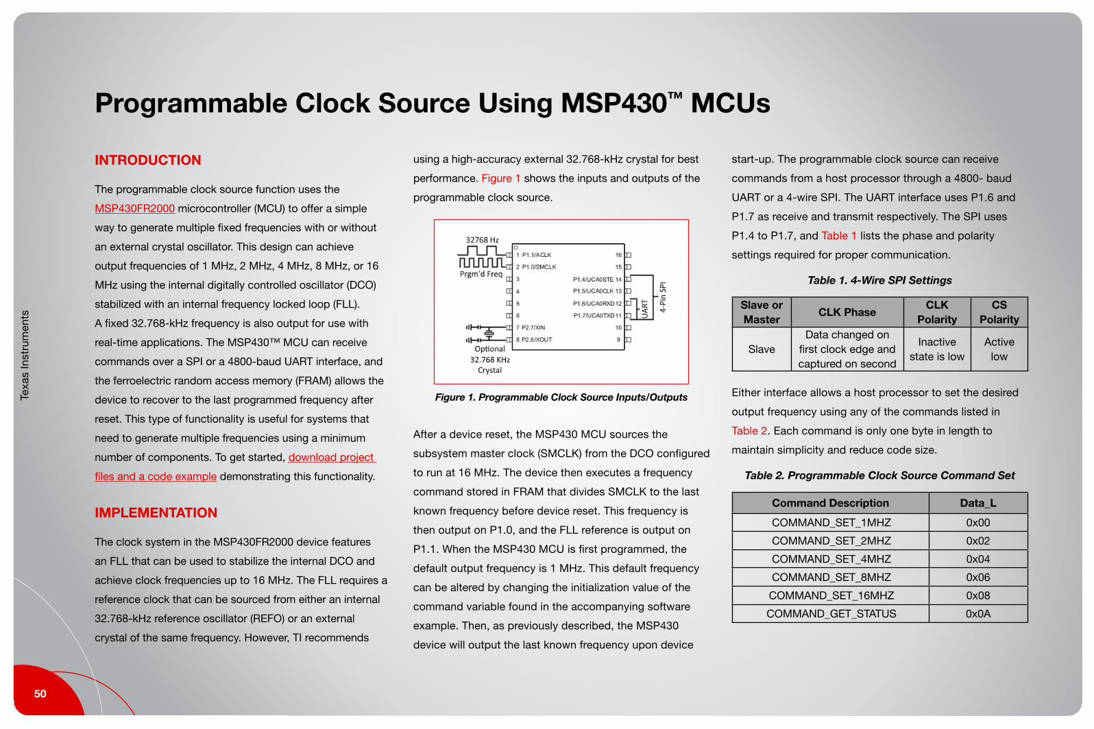
Texa
s In
stru
men
ts
50
INTRODUCTION
The programmable clock source function uses the
MSP430FR2000 microcontroller (MCU) to offer a simple
way to generate multiple fixed frequencies with or without
an external crystal oscillator . This design can achieve
output frequencies of 1 MHz, 2 MHz, 4 MHz, 8 MHz, or 16
MHz using the internal digitally controlled oscillator (DCO)
stabilized with an internal frequency locked loop (FLL) .
A fixed 32 .768-kHz frequency is also output for use with
real-time applications . The MSP430™ MCU can receive
commands over a SPI or a 4800-baud UART interface, and
the ferroelectric random access memory (FRAM) allows the
device to recover to the last programmed frequency after
reset . This type of functionality is useful for systems that
need to generate multiple frequencies using a minimum
number of components . To get started, download project
files and a code example demonstrating this functionality .
IMPLEMENTATION
The clock system in the MSP430FR2000 device features
an FLL that can be used to stabilize the internal DCO and
achieve clock frequencies up to 16 MHz . The FLL requires a
reference clock that can be sourced from either an internal
32 .768-kHz reference oscillator (REFO) or an external
crystal of the same frequency . However, TI recommends
using a high-accuracy external 32 .768-kHz crystal for best
performance . Figure 1 shows the inputs and outputs of the
programmable clock source .
Figure 1. Programmable Clock Source Inputs/Outputs
After a device reset, the MSP430 MCU sources the
subsystem master clock (SMCLK) from the DCO configured
to run at 16 MHz . The device then executes a frequency
command stored in FRAM that divides SMCLK to the last
known frequency before device reset . This frequency is
then output on P1 .0, and the FLL reference is output on
P1 .1 . When the MSP430 MCU is first programmed, the
default output frequency is 1 MHz . This default frequency
can be altered by changing the initialization value of the
command variable found in the accompanying software
example . Then, as previously described, the MSP430
device will output the last known frequency upon device
start-up . The programmable clock source can receive
commands from a host processor through a 4800- baud
UART or a 4-wire SPI . The UART interface uses P1 .6 and
P1 .7 as receive and transmit respectively . The SPI uses
P1 .4 to P1 .7, and Table 1 lists the phase and polarity
settings required for proper communication .
Table 1. 4-Wire SPI Settings
Slave or Master
CLK PhaseCLK
PolarityCS
Polarity
SlaveData changed on
first clock edge and captured on second
Inactive state is low
Active low
Either interface allows a host processor to set the desired
output frequency using any of the commands listed in
Table 2 . Each command is only one byte in length to
maintain simplicity and reduce code size .
Table 2. Programmable Clock Source Command Set
Command Description Data_L
COMMAND_SET_1MHZ 0x00
COMMAND_SET_2MHZ 0x02
COMMAND_SET_4MHZ 0x04
COMMAND_SET_8MHZ 0x06
COMMAND_SET_16MHZ 0x08
COMMAND_GET_STATUS 0x0A
Programmable Clock Source Using MSP430™ MCUs

51
Tips and tricks to enhance simple analog and digital functions
When using the UART interface, the MSP430 MCU will
respond with a single byte when a command has completed
execution . When using a SPI interface, the host processor
must use COMMAND_GET_STATUS to query the execution
status of the last command . Table 3 lists the three responses
that can be issued from the programmable clock source .
Table 3. Programmable Clock Source Responses
ResponseDescription Data_L
Command executed successfully 0x00
Incorrect command 0x01
Command is still being processed 0x02
PERFORMANCE
The programmable clock source can achieve 1-MHz,
2-MHz, 4-MHz, 8-MHz, or 16-MHz frequency output at
±2% accuracy using the internal REFO or ±0 .5% accuracy
using an external crystal . More detailed performance
specifications can be found in the clock specifications
section of the MSP430FR2000 MCU data sheet . Overall, the
accuracy and power consumption is improved when using
an external crystal oscillator .
Several design decisions were made to ensure the code
could fit into the limited 512-byte memory space of the
MSP430FR2000 device . Of these decisions, the 4800 baud
rate has the most affect .
In this application, the UART module receives its source
clock from either REFO or the 32 .678-kHz external crystal .
This was done so the baud rate registers did not need to
be altered when the user changed the device’s frequency .
Consequently, this greatly reduced the amount of code
required to implement UART communication . Finally, a baud
rate of 4800 was chosen because of the relatively low error
when compared to a 9600-baud rate source from a 32 .678-
kHz clock . There are no such limitations when using SPI
communication .
To ensure the clock source is always active, the deepest
low-power mode (LPM) the MSP430 MCU can enter is
LPM0 . Therefore the programmable clock source typically
consumes 402 μA of current at 3 V, regardless of the
selected output frequency .
Finally, the code has two infinite loops that have the
potential to keep the device from outputting the correct
frequency at startup . The first is a loop checking for the
external crystal stability . The second is a loop checking
for the FLL locking to a frequency of 16 MHz . When the
device is stuck in either loop, the response to sending a
COMMAND_GET_STATUS is always 0x02, as described in
Table 3 . If this problem occurs, reset the MSP430 MCU .
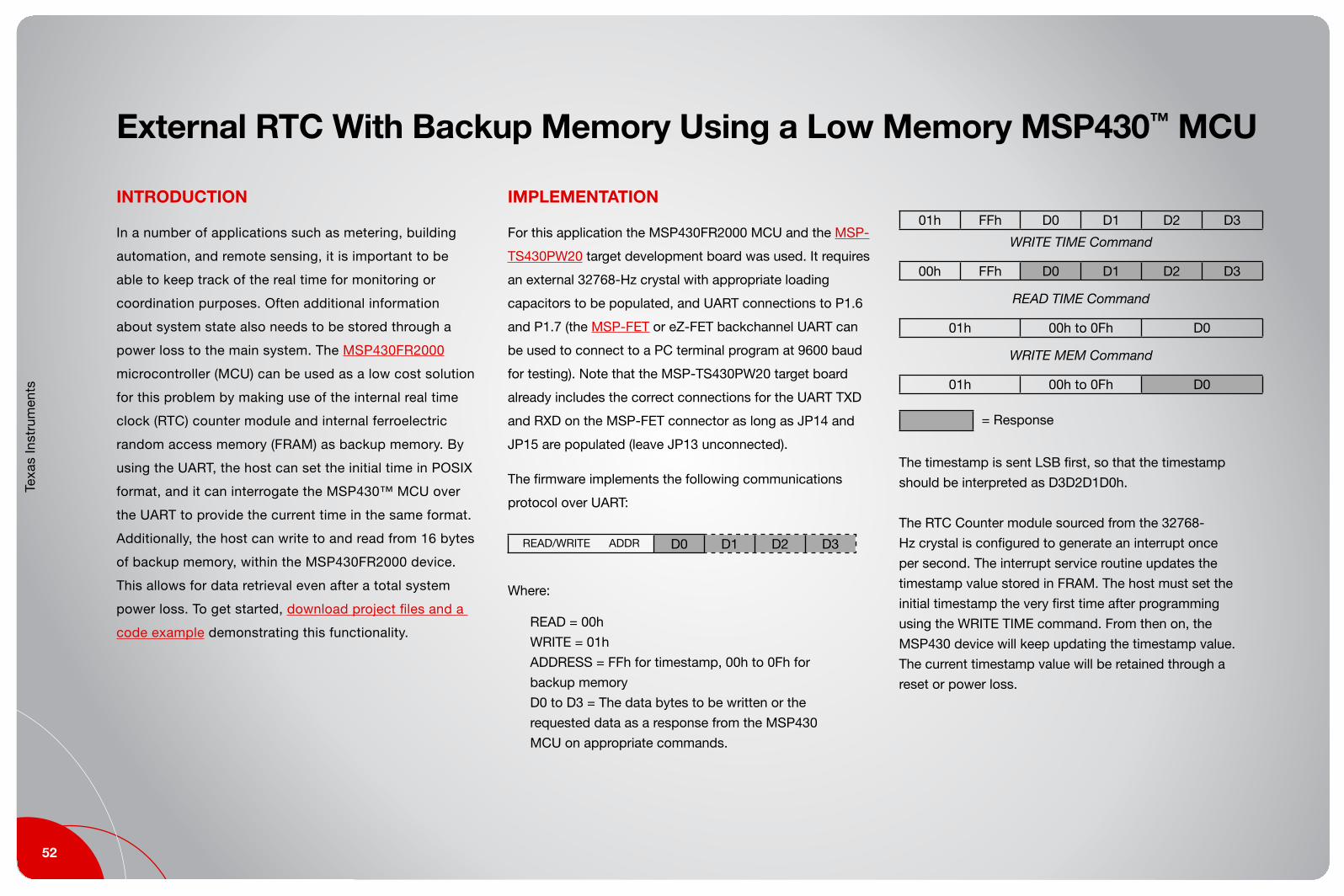
Texa
s In
stru
men
ts
52
INTRODUCTION
In a number of applications such as metering, building
automation, and remote sensing, it is important to be
able to keep track of the real time for monitoring or
coordination purposes . Often additional information
about system state also needs to be stored through a
power loss to the main system . The MSP430FR2000
microcontroller (MCU) can be used as a low cost solution
for this problem by making use of the internal real time
clock (RTC) counter module and internal ferroelectric
random access memory (FRAM) as backup memory . By
using the UART, the host can set the initial time in POSIX
format, and it can interrogate the MSP430™ MCU over
the UART to provide the current time in the same format .
Additionally, the host can write to and read from 16 bytes
of backup memory, within the MSP430FR2000 device .
This allows for data retrieval even after a total system
power loss . To get started, download project files and a
code example demonstrating this functionality .
IMPLEMENTATION
For this application the MSP430FR2000 MCU and the MSP-
TS430PW20 target development board was used . It requires
an external 32768-Hz crystal with appropriate loading
capacitors to be populated, and UART connections to P1 .6
and P1 .7 (the MSP-FET or eZ-FET backchannel UART can
be used to connect to a PC terminal program at 9600 baud
for testing) . Note that the MSP-TS430PW20 target board
already includes the correct connections for the UART TXD
and RXD on the MSP-FET connector as long as JP14 and
JP15 are populated (leave JP13 unconnected) .
The firmware implements the following communications
protocol over UART:
READ/WRITE ADDR D0 D1 D2 D3
Where:
READ = 00h
WRITE = 01h
ADDRESS = FFh for timestamp, 00h to 0Fh for
backup memory
D0 to D3 = The data bytes to be written or the
requested data as a response from the MSP430
MCU on appropriate commands .
01h FFh D0 D1 D2 D3
WRITE TIME Command
00h FFh D0 D1 D2 D3
READ TIME Command
01h 00h to 0Fh D0
WRITE MEM Command
01h 00h to 0Fh D0
= Response
The timestamp is sent LSB first, so that the timestamp
should be interpreted as D3D2D1D0h .
The RTC Counter module sourced from the 32768-
Hz crystal is configured to generate an interrupt once
per second . The interrupt service routine updates the
timestamp value stored in FRAM . The host must set the
initial timestamp the very first time after programming
using the WRITE TIME command . From then on, the
MSP430 device will keep updating the timestamp value .
The current timestamp value will be retained through a
reset or power loss .
External RTC With Backup Memory Using a Low Memory MSP430™ MCU
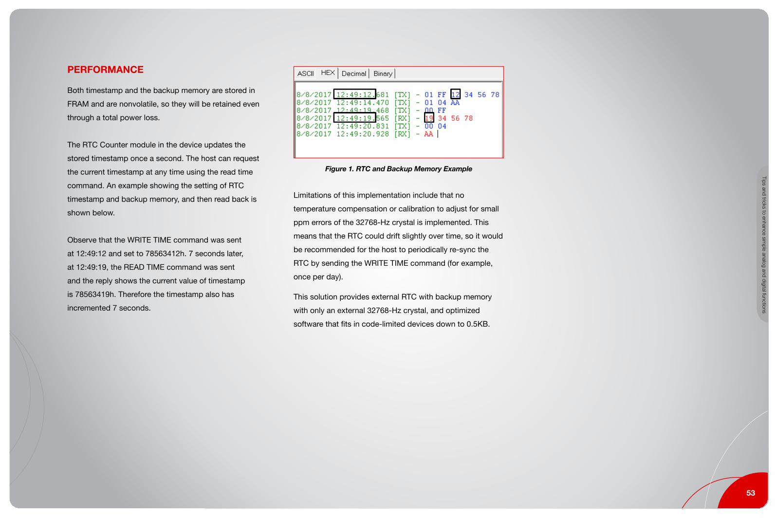
53
Tips and tricks to enhance simple analog and digital functions
PERFORMANCE
Both timestamp and the backup memory are stored in
FRAM and are nonvolatile, so they will be retained even
through a total power loss .
The RTC Counter module in the device updates the
stored timestamp once a second . The host can request
the current timestamp at any time using the read time
command . An example showing the setting of RTC
timestamp and backup memory, and then read back is
shown below .
Observe that the WRITE TIME command was sent
at 12:49:12 and set to 78563412h . 7 seconds later,
at 12:49:19, the READ TIME command was sent
and the reply shows the current value of timestamp
is 78563419h . Therefore the timestamp also has
incremented 7 seconds .
Figure 1. RTC and Backup Memory Example
Limitations of this implementation include that no
temperature compensation or calibration to adjust for small
ppm errors of the 32768-Hz crystal is implemented . This
means that the RTC could drift slightly over time, so it would
be recommended for the host to periodically re-sync the
RTC by sending the WRITE TIME command (for example,
once per day) .
This solution provides external RTC with backup memory
with only an external 32768-Hz crystal, and optimized
software that fits in code-limited devices down to 0 .5KB .

Texa
s In
stru
men
ts
54
Programmable System Wake-up Controller Using MSP430™ MCUs
INTRODUCTION
The programmable system wake-up controller function of
the MSP430FR2000 microcontroller (MCU) offers a simple
way to add an external, real-time, and lowpower wake-up
controller to an existing system . This type of system wake-
up controller is useful to applications that need to stay in
low-power modes for variable extended periods of time .
To get started, download project files and a code example
demonstrating this functionality . For a similar application,
but with consistent wake-up time, see Simple RTC-Based
System Wake-up Controller Using MSP430™ MCUs .
IMPLEMENTATION
A low-frequency 32 .768-kHz crystal is required for
this application . Alternatively, the internal trimmed
lowfrequency reference oscillator (REFO) can be used at
the cost of extra current . See the device-specific data
sheet for specifications . The wake-up time is sent to
the MSP430FR2000 MCU through SPI in the following
order: software counter (increment), RTCMOD high byte,
and RTCMOD low byte (see Table 1) . Table 2 lists the
SPI settings . At this point, the host should go into a low-
power or sleep mode as the real-time clock (RTC) starts
immediately after reception of the third byte . The line from
the MSP430 MCU to the host is used to communicate to the
host to wake-up from its low-power or sleep mode . This line
should be connected to an interruptible or wake-up capable
source pin on the host (see Figure 1) .
Figure 1. Programmable System Wake-up Controller Block Diagram
The wake-up time is a function of the RTC Counter
peripheral and software scaling factors . The RTC
Counter module in this application is clocked by XT1 at
approximately 32 .768 kHz . The largest predivider for the
module is 1024 . By using this divider value, every 32 counts
of the RTC Counter is 1 second . The RTCMOD register
holds a count value that gives an interrupt when the RTC
Counter counts to it . The RTCMOD register of the RTC
Counter is 16 bits wide so the maximum that time the RTC
Counter can count before overflow is approximately 34
minutes . For example, if a host wanted to setup a wake-
up time of 1 hour, it would send a value of 0x01E0FF over
SPI (see Table 1) . This means the host has set a counting
interval of one, with an RTCMOD value of 0xE0FF, which
corresponds to 30 minutes with the clock settings previously
discussed . Equation 1 and Equation 2 can be used to
calculate wake-up time in seconds in both a general case
and for the parameters described above .
RTCMOD ClockSource ClockPredivider
( )x increment = WakeUpTimeSeconds (1)
RTCMOD 32
x increment = WakeUpTimeSeconds (2)

55
Tips and tricks to enhance simple analog and digital functions
Figure 2 shows the code flow for the application . The
programmable wake-up controller is design to stay in low-
power mode 3 (LPM3) to conserve power . When the host
controller sends the 3 wake-up time bytes, the RTC starts
counting to the time value sent to the device . The RTC
interrupt manages the total wake-up time and sends a low-
to-high pulse to the host controller after the time value has
been reached . The host cannot start a new count or restart
the current count until the previous one has ended . To start
a new count, the host must send another set of wake-up
time bytes to the MSP430FR2000 MCU before going to
sleep again .
Table 2. 4-Wire SPI Connections
Slave or Master
CLK PhaseCLK
PolarityCS
Polarity
SlaveData changed on
first clock edge and captured on second
Inactive state is low
Active high,
idle low
Table 3. Average Power Consumption
Wake-up Time:
1 s 10 s 1 m* 1 h* 24 h*
Average Current:
1 .36 μA 1 .33 μA 1 .32 μA 1 .32 μA 1 .32 μA
*Estimated
Figure 2. Software Flow Diagram

Texa
s In
stru
men
ts
56
INTRODUCTION
Watchdog timers (WDTs) are particularly useful because
they detect if a microcontroller is in an invalid software
state and initiate a reset if needed . These invalid software
states can be caused by anything from a software bug to
electromagnetic interference . In general, a WDT resets the
system when it does not receive a regular pulsed signal from
the host processor .
In critical systems, such as smoke detectors and other
industrial applications, an invalid software state could be
catastrophic . In these instances, an external WDT would be
imperative . The external WDT has a separate clock source
providing redundancy and making the system more robust .
This solution presents a configurable external watchdog
timer that accepts watchdog time-out values ranging from
1 to 2 seconds, in increments of 200 ms . A shorter time-
out interval could be achieved, if needed, by changing
the values in the timeout array to match the application
specifications . This example has been optimized for lowest
code size, fitting in a lowcost 0 .5KB MSP430FR2000
microcontroller (MCU) . It also utilizes the MSP430™ ultra-
low-power operating states by going into low-power mode
3 (LPM3) when not executing a WDT-specific operation .
To get started, download project files and a code example
demonstrating this functionality .
IMPLEMENTATION
This solution uses an MSP430FR2000 MCU and any
external host processor with UART, reset, and GPIO
capability . This allows the reset line of the host processor
to be controlled by the low-cost MSP430FR2000 MCU with
0 .5KB of memory .
The reset pulse duration, initialized to 1 ms, is user
configurable inside of the source code by changing the
Reset_Cycles value . The watchdog interrupt (WDI) input
is a signal generated by the host processor to notify the
external WDT that it is working properly . A high-to-low
transition within every n seconds (specified by the timeout
selection value) keeps the external WDT from resetting the
host processor . As a typical default, the time-out value is
initialized to 1 .6 seconds .
The backchannel UART of the MSP-FET or eZ-FET on an
MSP430 LaunchPad™ development kit is used for the UART
communication with a terminal program on the PC to send
the commands for selecting each timeout value . Figure 1
shows how the MSP430FR2000 MCU can be connected to
an MCU to act as an external WDT .
Figure 1. External Watchdog Timer Hardware Block Diagram
The external WDT uses interrupts to wake up from low-
power mode to execute specific functions . Figure 2 shows
how the software works with the hardware to reliably
monitor a host processor .
External Programmable Watchdog Timer Using MSP430™ MCUs

57
Tips and tricks to enhance simple analog and digital functions
Figure 2. External Watchdog Timer Software Flow Chart
To run the demo on a PC, connect the LaunchPad kit or
target development board to the PC, load the code into the
device, allow the device to run, and end the debug session .
The MSP-TS430PW20 target development board already
includes the correct connections for the UART TXD and RXD
on the MSPFET connector as long as JP14 and JP15 are
populated (leave JP13 unconnected) .
At start-up, the code continues to send reset pulse signals
from P1 .3 unless it sees the watchdog being addressed by
the WDI pin . Figure 3 shows the logic analyzer output from
P1 .3 when the WDT is and is not being addressed .
Figure 3. Logic Analyzer Output When Addressing
and Not Addressing the WDT
In the top screenshot in Figure 3, the WDI input toggles
every 500 ms, thus meeting the default timeout requirement
and not causing the reset to be sent . In the bottom
screenshot in Figure 3, the WDI input is held low, thus
breaking the timing requirement and causing the reset line to
pulse low for the default time of 1 ms .
To take advantage of the backchannel UART on the MSP-FET
or the eZ-FET, use a terminal program on the PC set to 9600
baud, no parity, and 1 stop bit to select the time-out values .
There are six acceptable values, selectable by sending hex
values from 0 to 5 . Table 1 lists the valid UART commands .
Table 1. Valid UART Watchdog Time-out Values
UART Command (Hex) Time-out Value (Seconds)
0 11 1 .22 1 .43 1 .64 1 .85 2
An invalid UART command results in no change of the time-
out value .
PERFORMANCE
If a larger MSP430 microcontroller were used, then more
features could be added to the solution . The current
solution uses the internal reference oscillator running at
32768 Hz as the source for Timer_B, but an external crystal
could be used to improve timing accuracy and decrease
power consumption . More memory could allow a specific
sequence or UART communication protocol to address the
external WDT . Additional memory would also allow the user
to program more time-out values into the external WDT, in
addition to the six programmed in the provided example .
Using only the low-cost 0 .5KB MSP430FR2000 MCU, this
solution reliably monitors the state of a host processor and
works to protect it from hanging up in an invalid loop .

Texa
s In
stru
men
ts
58
INTRODUCTION
The simple system wake-up controller function of the
MSP430FR2000 microcontroller (MCU) offers a simple
way to add an external, real-time, and low-power wake-up
controller to an existing system . This type of system wake-
up controller is useful to applications that need to stay in
low-power modes for regular extended periods of time . One
example is battery-operated wireless sensing applications
that need to check in with central servers periodically while
otherwise staying in low-power modes . To get started,
download project files and a code example demonstrating
this functionality . For a similar application but with variable
wake-up time, see Programmable System Wake-up
Controller Using MSP430™ MCUs .
IMPLEMENTATION
A low-frequency 32 .768-kHz crystal is required for this
application . Alternatively, the internal trimmed lowfrequency
reference oscillator (REFO) can be used at the cost of
extra current . See the MSP430FR2000 MCU data sheet for
specifics . The wake-up time is decided at compile time for
the MSP430FR2000 device and cannot be changed when
in system . The interface for this function is two GPIO lines
(see Figure 1) . The host-to-MSP430 line is used to tell the
MSP430FR2000 device to start its real-time clock (RTC)
counting function . At this time, the host should go into
a low-power or sleep mode . The MSP430-tohost line is
used to communicate to the host to wake up from its low-
power or sleep mode . This line should be connected to an
interruptible or wake-up capable source pin on the host .
Figure 1. Simple System Wake-up Controller Block Diagram
The wake-up time is a function of the RTC Counter
peripheral and software scaling factors . The RTC
Counter module in this application is clocked by XT1 at
approximately 32 .768 kHz . The largest predivider for the
module is 1024 . By using this divider value, every 32 counts
of the RTC Counter is 1 second . The RTCMOD register
holds a count value that gives an interrupt when the RTC
Counter counts to it . The RTCMOD register of the RTC
Counter is 16 bits wide, so the maximum time the RTC
Counter can count before overflow is approximately 34
minutes . The example code uses a timing of 1 second and
provides an alternate value of 0xE0FF, which gives a period
of 30 minutes . In addition to the RTC Counter registers,
the code uses a software overflow counter to scale the
RTC Counter time to longer periods . The example code
defines the software overflow counter to be 1, and thus the
1-second (alternate: 30-minute) wake-up time is extended
to 2 seconds (alternate: 1 hour) . The user can change the
#define INCREMENT to increase the software overflow
counter interval . Equation 1 and Equation 2 can be used to
calculate wake-up time in seconds in both a general case
and for the parameters described above .
RTCMOD ClockSource ClockPredivider
( )x increment = WakeUpTimeSeconds (1)
RTCMOD 32
x increment = WakeUpTimeSeconds (2)
Simple RTC-Based System Wake-up Controller Using MSP430™ MCUs

59
Tips and tricks to enhance simple analog and digital functions
Figure 2 shows the code flow for the application . The simple
wake-up controller is design to stay in lowpower mode 3
(LPM3) to conserve power . When the host controller sends
a low-to-high transition pulse to the MSP430FR2000 MCU,
the RTC starts counting to the time value programmed into
the device . The RTC interrupt manages the total wake-up
time and sends a low-to-high pulse to the host controller
after the time value has been reached . When the host sends
the RTC start signal to the MSP430FR2000 device, this
GPIO interrupt is disabled until the programmed time value
has elapsed . The host cannot start a new count or restart
the current count until the previous one has ended . To
start a new count, the host must send another low-to-high
transition to the MSP430FR2000 MCU .
PERFORMANCE
Example code size is less than 200 bytes . Table 1 lists
the power consumption of the simple system wake-
up controller . The average current of the application
is dominated by the LPM3 current of the device and
approaches this level as the the wake-up time period
is extended . Table 1 lists measured values for 1- and
10-second wake-up intervals and calculated values for
longer time periods .
Table 1. Average Power Consumption
Wake-up Time:
1 s 10 s 1 m* 1 h* 24 h*
Average Current:
1 .5 μA 1 .06 μA 1 .00 μA<1 .00
μA
<1 .00
μA
*Estimated
Figure 2. Code Flow Diagram

Texa
s In
stru
men
ts
60
INTRODUCTION
Segment LED displays provide information to users in a wide
variety of applications from simple timers to smart meters
and more . This application uses three 7-segment LEDs to
display the time of a stopwatch . The demonstration uses
the MSP430FR2000 microcontroller (MCU) to implement the
stopwatch, because it is inexpensive and the code size less
than 512 bytes . To get started, download project files and a
code example demonstrating this functionality .
IMPLEMENTATION
This application uses a 4-digit 7-segment LED to display
the stopwatch time . The MCU measures the time using
the real-time clock (RTC) peripheral and utilizes general-
purpose output pins to drive the LEDs so that it displays
the time . There are two buttons to control the time . One is
to start and stop the stopwatch, and the other is to reset
the timer . The LEDs and the buttons are connected to the
MSP430FR2000 using digital I/O pins . Figure 1 shows the
stopwatch block diagram .
Figure 1. Stopwatch Block Diagram
P1 .0 to P1 .6 control the number displayed by setting
the voltage high to light the LEDs . P1 .7, P2 .0, and P2 .1
select which digit is shown by setting the voltage high to
make sure the right segments light up . In this design, the
current that is required by the LEDs is too large for the
MSP430FR2000 MCU . Therefore, P1 .7, P2 .0, and P2 .1 drive
external transistors to supply the current .
Figure 2 shows the outputs of P1 .7, P2 .0, and P2 .1 . To avoid
visible flickering, the frequency of refresh timing should
greater than 10 Hz . In this application, the refresh frequency
is approximately 3 .3 kHz .
Figure 1. Refresh Timing Diagram
First the desired digit is selected using P1 .7, P2 .0, and P2 .1,
then the number to be shown is controlled by P1 .0 to P1 .6 .
After that, change to a different LED to display the number
and repeat these steps . This design can show from 0 .1
second up to 99 .9 seconds . The unit can rescaled from 1
second to 999 seconds based on the application .
P2 .6 determines the start and stop function of the
stopwatch and detects the rising edge to trigger the start or
stop interrupt . The timer is stopped by default . Pressing the
P2 .6 button for the first time starts the timer, and pressing
the button a second time stops the timer .
7-Segment LED Stopwatch Using Low-Memory MSP430™ MCUs

61
Tips and tricks to enhance simple analog and digital functions
P2 .7 is used to control the restart function of the stopwatch
and detects the rising edge to trigger the restart interrupt . If
the restart interrupt is triggered, the timer resets to zero and
stops counting immediately .
Software or hardware methods can be used to avoid the
debounce on the push buttons . In this application, a low-
frequency hardware filter is used to avoid the issue .
This application uses the built-in RTC function of the
MSP430FR2000 MCU to calculate the time . The RTC is
sourced from the auxiliary clock (ACLK) source by the
reference oscillator (REFO, 32 .768 kHz) . This allows a
0 .1-second interrupt by dividing the ACLK by 64 and then
setting the RTC count as 51 (see Equation 1) .
0 .1 s ≈ (64 / 32768) × 51 (1)
Figure 3 shows the LED display of the stopwatch . Figure 3(a)
shows the initial state of the stopwatch, and Figure 3(b)
shows the operation of the stopwatch .
Figure 3. LED Display
PERFORMANCE
Using the MSP430FR2000 MCU has certain limitations
due to number of GPIO pins . The RTC Counter module in
the device uses the REFO instead of an external crystal
as the clock resource . The absolute calibrated tolerance
of the REFO based on the datasheet is –3 .5% to +3 .5%
when the temperature changes from –40°C to 85°C and the
supply voltage changes from 1 .8 V to 3 .6 V . Therefore, the
tolerance of this stopwatch is ±35 μs/s . If a better accuracy
is required, an external crystal can be used to supply the
clock for the system . If more GPIO pins or more memory are
needed to support additional digits or other functionality,
other MSP430™ MCUs can be used .
The design can be easily modified to create a countdown
timer by changing the RTC interrupt function to the
countdown mode .

Texa
s In
stru
men
ts
62
INTRODUCTION
Voltage monitoring is essential for battery- and buspowered
applications to save the system state through a power loss
event . Often the real time should be saved as a timestamp
to track the power loss event . The MSP430FR2000
microcontroller (MCU) can be used as a low-cost solution
for this problem by making use of the internal enhanced
comparator (eCOMP), real-time clock (RTC) counter, and
internal ferroelectric random access memory (FRAM) . By
using the UART, the host can set the initial time in POSIX
format, and it can interrogate the MSP430™ MCU over
the UART to provide the current time in the same format .
Additionally, the real time is saved as a timestamp in FRAM
during the power loss . To get started, download project files
and a code example demonstrating this functionality .
IMPLEMENTATION
This solution uses the internal comparator of the
MSP430FR2000 MCU and external resistors to monitor the
supply voltage . As the block diagram in Figure 1 shows, the
supply voltage is divided by resistors R1 and R2, and the
divided voltage (Vin) is connected to the comparator positive
input channel . The voltage is calculated by Equation 1 .
Vin = R1+R2
= 3
Vsupply x R1 Vsupply
(1)
The negative input of the comparator is connected to the
6-bit built-in digital-to-analog converter (DAC) . The internal
1 .5-V reference is selected as the DAC reference voltage .
The DAC output voltage is defined by the macro COMPTHR
in the firmware . Vth is the voltage threshold and is calculated
from Equation 2 .
Vth = 64
= 64
= 1VCOMPTHR x 1 .5V 43X1 .5V
(2)
The RTC module is used as an external RTC to provide
the current real time in POSIX format . The host can set the
initial time and then read the current time through a UART
interface . An external 32768-Hz crystal is used as the clock
source for the RTC and UART modules .
If the supply voltage falls below 3 V, Vin falls below 1 V, which
is lower than Vth, and a comparator interrupt is triggered .
In the comparator interrupt service routine, the current
timestamp is stored in FRAM to record the power loss event .
The eCOMP module supports programmable hysteresis
settings, and this demo uses the 30-mV hysteresis mode to
avoid false triggers . By changing the divider resistor and the
macro COMPTHR, different voltage levels can be monitored
based on application requirements .
Figure 1. Voltage Monitor Block Diagram
The comparator input voltage (Vin) is set by the ratio of the
two resistors in the divider . Keeping the ratio constant, there
are tradeoffs to consider for selecting the actual resistor
values . With higher resistances, the leakage current at
the comparator input can affect the Vin voltage accuracy .
With lower resistances, the current through the divider is
increased . For information on how to select optimally-sized
resistors, see Optimizing Resistor Dividers at a Comparator .
Another scenario is having one MCU GPIO instead of
ground connected to the R1 resistor . Setting the GPIO
output low can replace the ground connected to the R1
resistor, and setting the GPIO output high can reduce the
power consumption of the voltage divider .
Voltage Monitor With a Timestamp Using a Low-Memory MSP430™ MCU
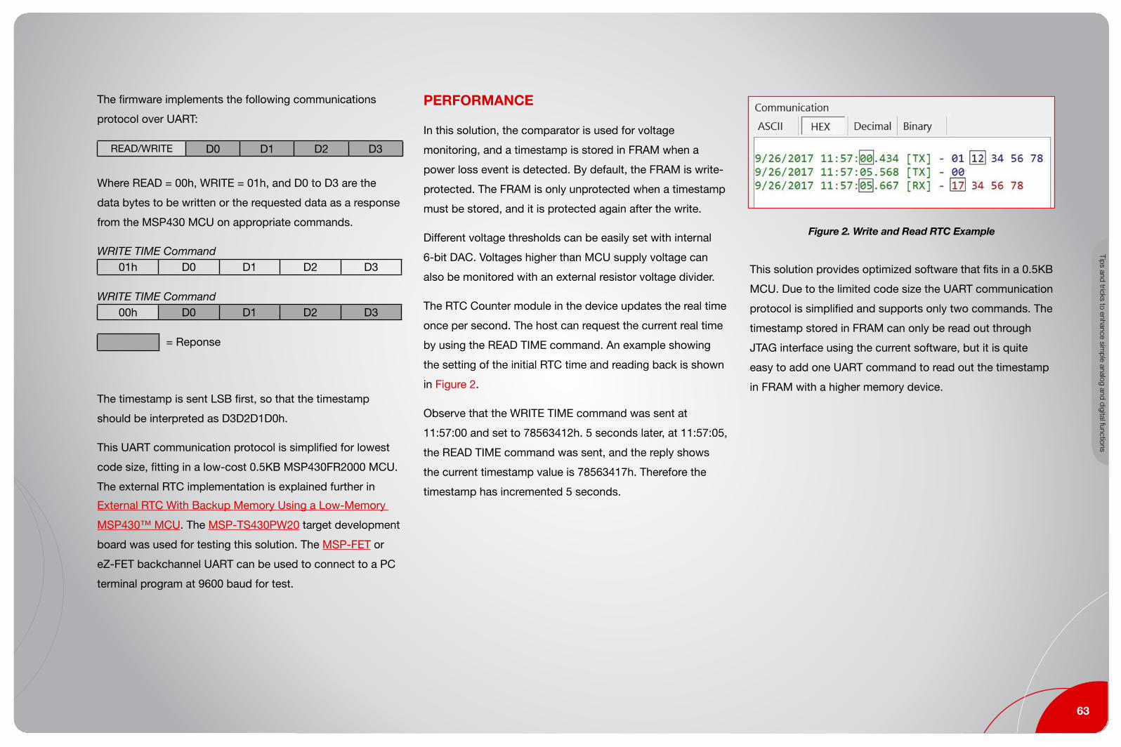
63
Tips and tricks to enhance simple analog and digital functions
The firmware implements the following communications
protocol over UART:
READ/WRITE D0 D1 D2 D3
Where READ = 00h, WRITE = 01h, and D0 to D3 are the
data bytes to be written or the requested data as a response
from the MSP430 MCU on appropriate commands .
WRITE TIME Command01h D0 D1 D2 D3
WRITE TIME Command00h D0 D1 D2 D3
= Reponse
The timestamp is sent LSB first, so that the timestamp
should be interpreted as D3D2D1D0h .
This UART communication protocol is simplified for lowest
code size, fitting in a low-cost 0 .5KB MSP430FR2000 MCU .
The external RTC implementation is explained further in
External RTC With Backup Memory Using a Low-Memory
MSP430™ MCU . The MSP-TS430PW20 target development
board was used for testing this solution . The MSP-FET or
eZ-FET backchannel UART can be used to connect to a PC
terminal program at 9600 baud for test .
PERFORMANCE
In this solution, the comparator is used for voltage
monitoring, and a timestamp is stored in FRAM when a
power loss event is detected . By default, the FRAM is write-
protected . The FRAM is only unprotected when a timestamp
must be stored, and it is protected again after the write .
Different voltage thresholds can be easily set with internal
6-bit DAC . Voltages higher than MCU supply voltage can
also be monitored with an external resistor voltage divider .
The RTC Counter module in the device updates the real time
once per second . The host can request the current real time
by using the READ TIME command . An example showing
the setting of the initial RTC time and reading back is shown
in Figure 2 .
Observe that the WRITE TIME command was sent at
11:57:00 and set to 78563412h . 5 seconds later, at 11:57:05,
the READ TIME command was sent, and the reply shows
the current timestamp value is 78563417h . Therefore the
timestamp has incremented 5 seconds .
Figure 2. Write and Read RTC Example
This solution provides optimized software that fits in a 0 .5KB
MCU . Due to the limited code size the UART communication
protocol is simplified and supports only two commands . The
timestamp stored in FRAM can only be read out through
JTAG interface using the current software, but it is quite
easy to add one UART command to read out the timestamp
in FRAM with a higher memory device .

Texa
s In
stru
men
ts
64
ABSTRACT
This guide is intended to help developers who are interested in testing code written
for the MSP430FR2000 MCU by loading it onto the MSP430FR2311 MCU . Running
the code on the MSP430FR2311 LaunchPad™ Development Kit may help to reduce
test costs, because the LaunchPad development kit with built-in eZ-FET emulation is
less expensive than purchasing the MSP-TS430PW20 Target Development Board and
MSP-FET Flash Emulation Tool .
Key differences between the two MCUs are outlined in this guide . These differences
may require a change in code when porting from the MSP430FR2000 MCU to the
MSP430FR2311 MCU .
CONTENTS
1 GPIO Multiplexing . . . . . . . . . . . . . . . . . . . . . . . . . . . . . . . . . . . . . . . . . . . . . . . . . . . . . . 65
1 .1 eUSCI_A0 UART and SPI Communication . . . . . . . . . . . . . . . . . . . . . . . . . . . . 65
1 .2 Timer0_B3 . . . . . . . . . . . . . . . . . . . . . . . . . . . . . . . . . . . . . . . . . . . . . . . . . . . . . 65
1 .3 Comparator . . . . . . . . . . . . . . . . . . . . . . . . . . . . . . . . . . . . . . . . . . . . . . . . . . . . 67
2 Porting from MSP430FR2311 to MSP430FR2000 . . . . . . . . . . . . . . . . . . . . . . . . . . . . . 68
LIST OF FIGURES
1 UART and SPI Signals . . . . . . . . . . . . . . . . . . . . . . . . . . . . . . . . . . . . . . . . . . . . . . . . . . . 65
2 Timer0_B3 Signals . . . . . . . . . . . . . . . . . . . . . . . . . . . . . . . . . . . . . . . . . . . . . . . . . . . . . 66
3 Comparator Signals . . . . . . . . . . . . . . . . . . . . . . . . . . . . . . . . . . . . . . . . . . . . . . . . . . . . 68
LIST OF TABLES
1 Comparison of MSP430FR2311 and MSP430FR2000 Features . . . . . . . . . . . . . . . 66-68
2 MSP430FR2311 Peripherals Not Available on MSP430FR2000 . . . . . . . . . . . . . . . . . . . 69
Code Porting From MSP430FR2000 to MSP430FR2311 MCUs

65
Tips and tricks to enhance simple analog and digital functions
1 GPIO MULTIPLEXING
1.1 eUSCI_A0 UART and SPI Communication
If the MSP430FR2000 code configures P1 .0, P1 .1, P1 .2, or P1 .3 for UART or SPI
communication, the code must be changed to instead use P1 .4, P1 .5, P1 .6, or P1 .7,
respectively (see Figure 1) . This is achieved by removing SYSCFG3 code and changing the
selection bits .
Figure 1. UART and SPI Signals
MSP430FR2000 MSP430FR2311
All Serial Communication
SYSCFG3 |= USCIARMP_1; ➝ //SYSCFG3 |= USCIARMP_1;
UART
P1SEL0 |= BIT2 | BIT3; ➝ P1SEL0 |= BIT6 | BIT7;
3-Wire SPI
P1SEL0 |= BIT1 | BIT2 | BIT3; ➝ P1SEL0 |= BIT5 | BIT6 | BIT7;
4-Wire SPI
P1SEL0 |= BIT0 | BIT1 | BIT2 | BIT3; ➝ P1SEL0 |= BIT4 | BIT5 | BIT6 | BIT7;
See Chapter 21 and Chapter 22 of the MSP430FR4xx and MSP430FR2xx Family User’s
Guide for more details about the Enhanced Universal Serial Communication Interface (eUSCI)
UART and SPI modes .
1.2 Timer0_B3
If the MSP430FR2000 code sets Timer0_B3 to use the capture input functionality on P2 .0 or
P2 .1 (CCIS in TB0CCTL0 is set to 00b or 01b and TBRMP in SYSCFG3 is set to 1), the input
pins must be changed to P1 .6 or P1 .7 .
Additionally, if the MSP430FR2000 code sets Timer0_B3 to output a PWM on P2 .0 or P2 .1 (P2 .0
or P2 .1 set to output and P2SEL set to 01b), the outputs must be changed to P1 .6 or P1 .7 .
Alternatively, to keep P2 .0 and P2 .1 as GPIOs when using the MSP430FR2311, the code can
be changed to use Timer1_B3 instead of Timer0_B3 (see Figure 2) . This involves changing
the register assignments from those for Timer0_B3 to Timer1_B3 . In most cases, it is
sufficient to perform a find and replace search of “TB0” to “TB1” and to update the interrupt
service routine, if present .

Texa
s In
stru
men
ts
66
Figure 2. Timer0_B3 Signals
The following comparison summarizes how to update the code to change from using P2 .0
and P2 .1 to P1 .6 and P1 .7 .
MSP430FR2000 MSP430FR2311
P2.0 set to TB0.CCI1A P1.6 set to TB0.CCI1A
SYSCFG3 |= TBRMP_1; //SYSCFG3 |= TBRMP_1;
TB0CCTL0 |= CCIS_0; ➝ TB0CCTL0 |= CCIS_0;
P2DIR &= ~BIT0 P1DIR &= ~BIT6
P2SEL0 |= BIT0; P1SEL1 |= BIT6;
P2.1 set to TB0.CCI2A P1.7 set to TB0.CCI2A
SYSCFG3 |= TBRMP_1; //SYSCFG3 |= TBRMP_1;
TB0CCTL0 |= CCIS_0; TB0CCTL0 |= CCIS_0;
P2DIR &= ~BIT1 ➝ P1DIR &= ~BIT7
P2SEL0 |= BIT1; P1SEL1 |= BIT7;
P2.0 set to TB0.1 P1.6 set to TB0.1
P2DIR |= BIT0; ➝ P1DIR |= BIT6;
P2SEL0 |= BIT0; P1SEL1 |= BIT6;
P2.1 set to TB0.2 P1.7 set to TB0.2
P2DIR |= BIT1; ➝ P1DIR |= BIT7;
P2SEL0 |= BIT1; P1SEL1 |= BIT7;

67
Tips and tricks to enhance simple analog and digital functions
The following comparison summarizes how to update the code to change from using Timer0_B3 to Timer1_B3 .
MSP430FR2000 MSP430FR2311
P2.0 set to TB0.CCI1A P2.0 set to TB1.CCI1ASYSCFG3 |= TBRMP_1; //SYSCFG3 |= TBRMP_1; TB0CCTL0 |= CCIS_0; TB1CCTL0 |= CCIS_0; P2DIR &= ~BIT0 ➝ P2DIR &= ~BIT0 P2SEL0 |= BIT0; P2SEL0 |= BIT0;
P2.1 set to TB0.CCI2A P2.1 set to TB1.CCI2ASYSCFG3 |= TBRMP_1; //SYSCFG3 |= TBRMP_1; TB0CCTL0 |= CCIS_1; TB1CCTL0 |= CCIS_1; P2DIR &= ~BIT1 ➝ P2DIR &= ~BIT1 P2SEL0 |= BIT1; P2SEL0 |= BIT1;
Outputting PWM on P2.0 and P2.1 P2DIR |= BIT0 | BIT1; P2DIR |= BIT0 | BIT1; P2SEL0 |= BIT0 | BIT1; P2SEL0 |= BIT0 | BIT1; // Setup Timer0_B // Setup Timer1_B TB0CCR0 = 100-1; TB1CCR0 = 100-1; TB0CCTL1 = OUTMOD_7; ➝ TB1CCTL1 = OUTMOD_7; TB0CCR1 = 75; TB1CCR1 = 75; TB0CCTL2 = OUTMOD_7; TB1CCTL2 = OUTMOD_7;TB0CCR2 = 25; TB1CCR2 = 25;TB0CTL = TBSSEL_1 | MC_1 | TBCLR; TB1CTL = TBSSEL_1 | MC_1 | TBCLR;
Timer Interrupt Service Routine #if defined(__TI_COMPILER_VERSION__) || #if defined(__TI_COMPILER_VERSION__) || defined(__IAR_SYSTEMS_ICC__) defined(__IAR_SYSTEMS_ICC__) #pragma vector = TIMER0_B1_VECTOR #pragma vector = TIMER1_B1_VECTOR __interrupt void Timer0_B1_ISR(void) __interrupt void Timer1_B1_ISR(void) #elif defined(__GNUC__) #elif defined(__GNUC__) void __attribute__ void __attribute__ ((interrupt(TIMER0_B1_VECTOR))) ((interrupt(TIMER1_B1_VECTOR))) Timer0_B1_ISR (void) Timer1_B1_ISR (void) #endif ➝ #endif { { switch(__even_in_range(TB0IV,TB0IV_TBIFG)) switch(__even_in_range(TB1IV,TB1IV_TBIFG)) { { case TB0IV_NONE: break; case TB0IV_TBCCR1: break; case TB0IV_TBCCR2: break; case TB0IV_TBIFG: break; default: break; } } } }
See Chapter 12 and Chapter 13 of the MSP430FR4xx and MSP430FR2xx Family User’s
Guide for more details about Timer_A and Timer_B .
1.3 Comparator
If the MSP430FR2000 code selects P1 .2 or P1 .3 as an input to the comparator, these pins
should be changed to P1 .0 or P1 .1 (see Figure 3) .
MSP430FR2000 MSP430FR2311
P1.2 set to C2 for CPPSEL P1.0 set to C0 as CPPSEL P1SEL0 |= BIT2; ➝ P1SEL0 |= BIT0; P1SEL1 |= BIT2; P1SEL1 |= BIT0; CPCTL0 |= CPPSEL_2; CPCTL0 |= CPPSEL_0;
P1.3 set to C3 for CPNSEL P1.1 set to C1 for CPNSEL P1SEL0 |= BIT3; P1SEL0 |= BIT1; P1SEL1 |= BIT3; ➝ P1SEL1 |= BIT1; CPCTL0 |= CPNSEL_3; CPCTL0 |= CPNSEL_1;
case TB1IV_NONE: break;case TB1IV_TBCCR1: break;case TB1IV_TBCCR2: break;case TB1IV_TBIFG: break;default: break;

Texa
s In
stru
men
ts
68
Figure 3. Comparator Signals
See Section 6 .11 .12 eCOMP0 of the MSP430FR231x Mixed-Signal Microcontrollers data
sheet and Chapter 17 of the MSP430FR4xx and MSP430FR2xx Family User’s Guide
for more details about using the comparator .
2 PORTING FROM MSP430FR2311 TO MSP430FR2000
The MSP430FR2311 MCU has features not available on the MSP430FR2000, so care should
be taken if code is developed on the MSP430FR2311 for the MSP430FR2000 . Table 1
summarizes differences between the two MCUs .
Table 1. Comparison of MSP430FR2311 and MSP430FR2000 Features
Feature MSP430FR2311 MSP430FR2000
Nonvolatile memory (KB) 4 0 .5 4 0 .5
RAM (KB) 1 0 .5
GPIO pins 16 12
I2C 1 0
SPI 2 1
ADC10-bit ADC(8 channels)
Slope
Comparators 2 4
Timers (16-bit) 2 1
Active power (μA/MHz) 126 120
Approximate price (US$) 0 .56 | 1ku 0 .29 | 1ku
For more comparisons between these and other MCU architectures, visit MSP430™ ultra-
low-power MCUs . Table 2 summarizes peripherals of the MSP430FR2311 that are not
present on the MSP430FR2000 .

69
Tips and tricks to enhance simple analog and digital functions
Table 2. MSP430FR2311 Peripherals Not Available on MSP430FR2000
Function Signal Name Pin Name PxDIR.x PxSELx Description
ADC
A0 P1 .0 X 11 Analog input A0
A1 P1 .1 X 11 Analog input A1
A2 P1 .2 X 11 Analog input A2
A3 P1 .3 X 11 Analog input A3
A4 P1 .4 X 11 Analog input A4
A5 P1 .5 X 11 Analog input A5
A6 P1 .6 X 11 Analog input A6
A7 P1 .7 X 11 Analog input A7
Veref+ P1 .0 X 11 ADC positive reference
Veref- P1 .2 X 11 ADC negative reference
TIA0
TRI0+ P1 .7 X 11 TIA0 positive input
TRI0- P1 .6 X 11 TIA0 negative input
TRI0O P1 .5 X 11 TIA0 output
SAC0
OA0+ P1 .4 X 11 SAC0, OA positive input
OA0- P1 .2 X 11 SAC0, OA negative input
OA0O P1 .3 X 11 SAC0, OA output
GPIO
P1 .4 P1 .4 I: 0; O: 1 00GPIO that can be configured for edge-selectable interrupt and for LPM3 .5, LPM4, and LPM4 .5 wake-up input capability
P1 .5 P1 .5 I: 0; O: 1 00
P1 .6 P1 .6 I: 0; O: 1 00
P1 .7 P1 .7 I: 0; O: 1 00
P2 .2 P2 .2 I: 0; O: 1 00 General-purpose I/O
P2 .3 P2 .3 I: 0; O: 1 00 General-purpose I/O
P2 .4 P2 .4 I: 0; O: 1 00 General-purpose I/O
P2 .5 P2 .5 I: 0; O: 1 00 General-purpose I/O
Function Signal Name Pin Name PxDIR.x PxSELx Description
I2CUCB0SCL P1 .3, P2 .5(1) X 01 eUSCI_B0 I2C clock
UCB0SDA P1 .2, P2 .4(1) X 01 eUSCI_B0 I2C data
SPI
UCB0STE P1 .0, P2 .2(1) X 01 eUSCI_B0 slave transmit enable
UCB0CLK P1 .1, P2 .3(1) X 01 eUSCI_B0 clock input/output
UCB0SIMO P1 .2, P2 .4(1) X 01 eUSCI_B0 SPI slave in/master out
UCB0SOMI P1 .3, P2 .5(1) X 01 eUSCI_B0 SPI slave out/master in
Timer_B
TB1 .CCI1AP2 .0
001
Timer TB1 CCR1 capture: CCI1A input, compare: Out1 outputTB1 .1 1
TB1 .CCI2AP2 .1
001
Timer TB1 CCR2 capture: CCI2A input, compare: Out2 outputTB1 .2 1
TB1CLK P2 .2 0 10 Timer clock input TBCLK for TB1
TB1TRG P2 .3 0 10TB1 external trigger input for TB1OUTH
1 This is the remapped functionality controlled by the USCIBRMP bit of the SYSCFG2 register. Only one selected port is valid at any time.
Table 2. MSP430FR2311 Peripherals Not Available on MSP430FR2000 (cont)

Texa
s In
stru
men
ts
70
ABSTRACT
When choosing a microcontroller (MCU), the amount of code space or nonvolatile
memory in the device is often a key consideration . To efficiently fit as much
functionality as possible into a device, there are considerations that can be given
when writing and building code to get the most optimized code size . This application
note outlines a number of optimization settings for Code Composer Studio™ (CCS)
and IAR Embedded Workbench® (IAR EW430) compilers that can make a big impact
on code size, as well as coding techniques for user code to build with optimal size .
CONTENTS
1 Introduction . . . . . . . . . . . . . . . . . . . . . . . . . . . . . . . . . . . . . . . . . . . . . . . . . . . . . . . . . . . 71
2 C Compiler Optimization . . . . . . . . . . . . . . . . . . . . . . . . . . . . . . . . . . . . . . . . . . . . . . . . . 71
2 .1 CCS . . . . . . . . . . . . . . . . . . . . . . . . . . . . . . . . . . . . . . . . . . . . . . . . . . . . . . . . . . 71
2 .2 IAR . . . . . . . . . . . . . . . . . . . . . . . . . . . . . . . . . . . . . . . . . . . . . . . . . . . . . . . . . . . 75
3 Coding Techniques . . . . . . . . . . . . . . . . . . . . . . . . . . . . . . . . . . . . . . . . . . . . . . . . . . . . . 78
3 .1 Use Smallest Possible Types for Variables and Constants . . . . . . . . . . . . . . . . 78
3 .2 Avoid Multiply and Divide . . . . . . . . . . . . . . . . . . . . . . . . . . . . . . . . . . . . . . . . . 78
3 .3 Use Lookup Tables Instead of Calculating . . . . . . . . . . . . . . . . . . . . . . . . . . . . 79
3 .4 Use Word Accesses to Registers . . . . . . . . . . . . . . . . . . . . . . . . . . . . . . . . . . . . 79
3 .5 Write to Registers Only Once (Where Possible) . . . . . . . . . . . . . . . . . . . . . . . . . 80
3 .6 Use the __even_in_range() Intrinsic . . . . . . . . . . . . . . . . . . . . . . . . . . . . . . . . . . 80
3 .7 Use Functions Judiciously and Write for Reuse and Commonality . . . . . . . . . . 81
4 Summary . . . . . . . . . . . . . . . . . . . . . . . . . . . . . . . . . . . . . . . . . . . . . . . . . . . . . . . . . . . . . 81
5 References . . . . . . . . . . . . . . . . . . . . . . . . . . . . . . . . . . . . . . . . . . . . . . . . . . . . . . . . . . . 81
Optimizing C Code for Size With MSP430™ MCUs: Tips and Tricks
Code Composer Studio, MSP430 are trademarks of Texas Instruments . IAR Embedded Workbench is a registered trademark of IAR Systems . All other trademarks are the property of their respective owners .

71
Tips and tricks to enhance simple analog and digital functions
1 INTRODUCTION
Changing just a few key lines of code and a few compiler settings can make a big difference
when it comes to code size . The code sizes used as an example in this application report
are using the code example Msp430fr211x_euscia0_uart_03 .c, which can be built for the
MSP430FR2000 MCU, which contains only 0 .5KB of FRAM . Code sizes listed were built with
CCS version 7 .3 with compiler 16 .9 .4 .LTS or IAR EW430 version 7 .10 .4 .
2 C COMPILER OPTIMIZATION
While working in C is typically preferred over assembly for its easy readability, writing in C
can add some overhead that starts to become non-trivial when using a device with limited
code space . However, through careful usage of compiler settings and features like global
variables, programming in C can become close to assembly programming in efficiency (and
still allowing for the compiler to do the heavy code optimization work rather than hand-
optimizing assembly code) .
No matter which IDE is used, the compiler already includes many tools for optimizing C code .
Understanding the settings available and what they mean allows the user to work with the
compiler to get the best code optimization results .
2.1 CCS
2.1.1 OPTIMIZATION SETTINGS
The main control of the compiler optimization is through the optimization settings accessible
within the IDE . The settings allow the user to select how aggressive they want the compiler to
apply optimization (which kinds of optimizations it is allowed to use) and the desired balance
of optimizing for code size vs execution speed .
In CCS, the optimization settings are found in Project > Properties > Build > MSP430
Compiler > Optimization . There are two main optimization settings: Optimization level, and
Speed vs size trade-offs (see Figure 1) .
Figure 1. CCS Optimization Settings
The optimization level determines what types of optimizations the compiler is allowed to make . Speed
vs size setting tells the compiler if trade-offs should be made more in the favor of size or speed, with
0 being optimizing with the most focus on size, and level 5 being the most focus on speed . Settings
between 0 and 5 instruct the compiler to take a more balanced approach . For more information, see the
MSP430 Optimizing C/C++ Compiler User’s Guide .
CCS provides a tool called the Optimizer Assistant (View > Optimizer Assistant) that can be
used to decide the optimal set of compiler settings for a particular project to fit in its target
device (see Figure 2) .

Texa
s In
stru
men
ts
72
Figure 2. Optimizer Assistant
After clicking Start Analysis, select which build option to vary: speed vs size trade-offs or
optimization level . The analysis then runs, varying the selected build option accordingly . The
other build option uses whatever is currently in the project settings and remains constant
through the test . For example, if the tool varies size vs speed setting, it uses whichever
optimization level is currently selected in the project settings for all of the builds (see Figure 3) .
Figure 3. Varying Size vs Speed in Optimizer Assistant
The Optimizer Assistant displays the code size for the different settings . Red indicates if the
code cannot fit in the selected device for the project, yellow indicates that the code fits the
device but a better option is available, and green indicates the recommended option for best
execution speed performance while still fitting into the target device memory . The check
mark indicates the current selection in the project settings . For more information about using
Optimizer Assistant, see http://processors .wiki .ti .com/index .php/Optimizer_Assistant
NOTE: After running the Optimizer Assistant, set the desired optimization settings in Project > Properties > Build > MSP430 Compiler > Optimization to apply them in subsequent builds .
2.1.2 CODE AND DATA MODEL
MSP430™ microcontrollers have a 16-bit architecture . However, larger MSP430 devices have
code space that extends to addresses 10000h and beyond, requiring 20 bits to store the full
address . The MSP430X CPU architecture featured on these devices includes an extended
instruction set to support operations on these 20-bit addresses . These extended instructions
can take additional CPU cycles and increased program space due to requiring an extension
word for double-operand instructions (see the appropriate family user’s guide chapter on
CPUX for more information on the extended instruction set) . Therefore, on small memory
devices where no addresses above 10000h exist in the device, it is important to ensure that
only the base 16-bit instruction set is used to build with the smallest possible code size . This
can be controlled by selecting the correct code and data model in the IDE project settings .
In CCS, go to Project > Properties > Build > MSP430 Compiler > Processor Options . Then
select Small Code Memory Model and Small Data Memory Model (see Figure 4) .
Figure 4. Code and Data Memory Model in CCS

73
Tips and tricks to enhance simple analog and digital functions
The build takes several minutes the very first time after changing the code and data model,
because the runtime support (RTS) library is built . Subsequent builds are much faster,
because the library is not rebuilt . Changing code and data model can have a huge effect on
the code size . Building the msp430fr211x_euscia0_uart_03 .c with large code model and full
optimization for code size builds to 928 bytes (see Figure 5) .
Figure 5. msp430fr211x_euscia0_uart_03.c With Large Memory Model
After changing the code and data model to small, the code size builds to 572 bytes - a 38% reduction
(see Figure 6) .
Figure 6. msp430fr211x_euscia0_uart_03.c With Small Memory Model
2.1.3 GLOBAL VARIABLES AND INITIALIZATION SETTINGS
The C-compiler inserts some initialization code from the runtime support (RTS) library
that runs every time the device starts up . This code does prepares the C environment by
setting up the stack and initializing variables in RAM . The initialization routines used by the
C-compiler by default use a compressed table of global variable initialization data, which
makes sense for large projects with large numbers of global variables, large arrays, and other
data that need to be initialized in the RAM at device start-up . However, for small devices that
contain simple code containing a small number of global variables, this code is no longer
space efficient . The crossover point is where the C-initialization code takes up more space
than directly initializing the variables with user code (not using compression) .
To understand how much space the C-start-up code is taking up in the part, look at the .map
file (found in the Debug folder after building) . Under the Section Allocation Map portion of the
linker file, find “ .text” . Here, you can see the start address and length for all functions in your
project, including functions inserted by the compiler from the RTS library . Functions from the
RTS library are all marked as from rts430x_xx_xx_eabi .lib (the xx differs depending on code
and data memory model selection) . The boxed functions in Figure 7 are all used for global
variable initialization – copy tables and decompression code including multiplication functions .
These functions require significant code space if working with a very code-limited part, such as
the MSP430FR2000 or MSP430G2001 MCU with only 512 bytes of FRAM or flash .
Figure 7. Default Global Variable Initialization in CCS
Therefore, for small devices in which code size is a concern, the following methods should
be employed to control the initialization of global variables . Option 1: If it is possible in the
application, simply eliminate use of global variables . This eliminates the overhead for initializing
global variables at start-up . Option 2: Use a limited number of global variables . Set up these
variables such that they are not preinitialized by the RTS library, using compiler settings .
Instead, initialize the global variables in main() with user code . Section 2 .1 .3 .1 includes steps to
address this .
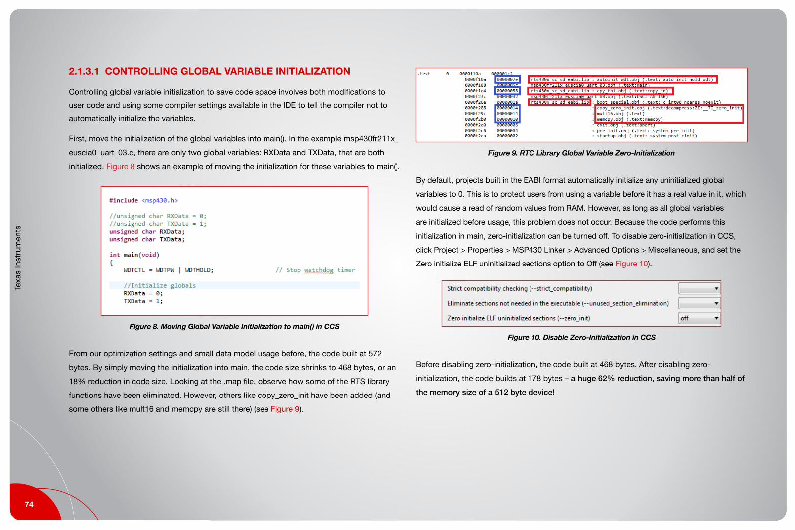
Texa
s In
stru
men
ts
74
2.1.3.1 CONTROLLING GLOBAL VARIABLE INITIALIZATION
Controlling global variable initialization to save code space involves both modifications to
user code and using some compiler settings available in the IDE to tell the compiler not to
automatically initialize the variables .
First, move the initialization of the global variables into main() . In the example msp430fr211x_
euscia0_uart_03 .c, there are only two global variables: RXData and TXData, that are both
initialized . Figure 8 shows an example of moving the initialization for these variables to main() .
Figure 8. Moving Global Variable Initialization to main() in CCS
From our optimization settings and small data model usage before, the code built at 572
bytes . By simply moving the initialization into main, the code size shrinks to 468 bytes, or an
18% reduction in code size . Looking at the .map file, observe how some of the RTS library
functions have been eliminated . However, others like copy_zero_init have been added (and
some others like mult16 and memcpy are still there) (see Figure 9) .
Figure 9. RTC Library Global Variable Zero-Initialization
By default, projects built in the EABI format automatically initialize any uninitialized global
variables to 0 . This is to protect users from using a variable before it has a real value in it, which
would cause a read of random values from RAM . However, as long as all global variables
are initialized before usage, this problem does not occur . Because the code performs this
initialization in main, zero-initialization can be turned off . To disable zero-initialization in CCS,
click Project > Properties > MSP430 Linker > Advanced Options > Miscellaneous, and set the
Zero initialize ELF uninitialized sections option to Off (see Figure 10) .
Figure 10. Disable Zero-Initialization in CCS
Before disabling zero-initialization, the code built at 468 bytes . After disabling zero-
initialization, the code builds at 178 bytes – a huge 62% reduction, saving more than half of
the memory size of a 512 byte device!

75
Tips and tricks to enhance simple analog and digital functions
2.2 IAR
2.2.1 OPTIMIZATION SETTINGS
The main control of the compiler optimization is through the optimization settings accessible
within the IDE . The settings allow the user to select how aggressively the compiler should
apply optimization (which kinds of optimizations it is allowed to use) and the desired balance
of optimizing for code size vs execution speed .
In IAR, the optimization settings are found in the Project > Options > C/C++ Compiler >
Optimizations tab . There are two main optimization settings: optimization level, and speed vs
size trade-offs (see Figure 11) .
Figure 11. Optimization Settings in IAR
The optimization level determines what types of optimizations the compiler is allowed to make . Speed
vs size setting tells the compiler if trade-offs should be made more in the favor of size or speed, with
speed, size, and balanced options . There are also options for what types of optimizations to allow under
enabled transformations . For more information, see the IAR C/C++ Compiler User’s Guide included with
IAR under Help .
2.2.2 CODE AND DATA MODEL
MSP430 microcontrollers have a 16-bit architecture . However, larger MSP430 devices have
code space that extends to addresses 10000h and beyond, requiring 20 bits to store the full
address . The MSP430X CPU architecture featured on these devices includes an extended
instruction set to support operations on these 20-bit addresses . These extended instructions
can take additional CPU cycles and increased program space due to requiring and extension
word for double-operand instructions (see the appropriate family user’s guide chapter on
CPUX for more information on the extended instruction set) . Therefore, on small memory
devices where no addresses above 10000h exist in the device, it is important to ensure that
only the base 16-bit instruction set is used to build with the smallest possible code size . This
can be controlled by selecting the correct code and data model in the IDE project settings .
In IAR, go to Project > Options > General Options > Target tab . Then select Small for Code
Model and Small for Data Model (see Figure 12) .
Figure 12. Small Code Model in IAR

Texa
s In
stru
men
ts
76
Changing code and data model can have an effect on the code size in some cases . Often,
the IAR compiler already accounts for this, but it is still good practice if no upper memory is
available or needed . The example msp430fr211x_euscia0_uart_03 .c builds to 239 bytes in IAR
for both large or small code model, but for some devices or code there can be a difference .
2.2.3 GLOBAL VARIABLES AND INITIALIZATION SETTINGS
The C-compiler inserts initialization code from the support library that runs every time the
device starts up . This code prepares the C environment by setting up the stack and initializing
variables in RAM . The initialization routines used by the C-compiler by default use initialization
methods that make sense for large projects or for the general case . However, for very small
devices that contain simple code containing a small number of global variables, this code is not
always the most space efficient . The crossover point is where the C-initialization code takes up
more space than directly initializing the variables with user code .
To understand how much space the C-start-up code uses, look at the .map file (found in
the Output folder after building) . Open Project > Options > Linker > List and check Module
Summary . Then in the .map file, under the Module Summary portion near the end of the linker
file, see the modules listed . This section lists he start address and length for the code and the
functions inserted by the compiler from the library . Functions from the library are all marked
starting with ? . The boxed functions in Figure 13 are all used for global variable initialization –
memcpy, zero-initialization of memory, C-start-up environment initialization, and exit routines .
These functions require significant code space if working with a very code-limited part, such
as the MSP430FR2000 or MSP430G2001 MCU with only 512 bytes of FRAM or flash .
Figure 13. Default Global Variable Initialization in IAR
Therefore, for small devices where code size is a concern, the following methods should be
employed to control the initialization of global variables .
Option 1: If it is possible in the application, simply eliminate use of global variables . This
eliminates the overhead for initializing global variables at start-up .
Option 2: Use a limited number of global variables . Set up these variables such that they are
not preinitialized by the library, using compiler settings . Instead, initialize the global variables
in main() with user code . Section 2 .2 .3 .1 includes steps to address this .

77
Tips and tricks to enhance simple analog and digital functions
2.2.3.1 CONTROLLING GLOBAL VARIABLE INITIALIZATION
Controlling global variable initialization to save code space involves both modifications to
user code, as well as using some compiler settings available in the IDE to tell the compiler
not to automatically initialize the variables .
First, move the initialization of the global variables into main() . In the example msp430fr211x_
euscia0_uart_03 .c, there are only two global variables: RXData and TXData, that are both
initialized . Figure 14 shows an example of moving the initialization for these variables to main() .
Figure 14. Moving Global Variable Initialization to main() in IAR
From the optimization settings and small data model usage before, the code built at 240
bytes . By simply moving the initialization into main, the code size shrinks to 210 bytes, or
12 .5% reduction in code size .
In the .map file (see Figure 15), observe how some of the library functions (for example,
memcpy) have been eliminated . However, others like memzero are still there . Further, the
cstart module has become smaller .
Figure 15. Global Variable Zero-initialization in IAR
By default, projects built in the EABI format automatically initialize any uninitialized global
variables to 0 . This is to protect users from using a variable before it has a real value in
it, which would read random values from RAM . However, as long as all global variables
are initialized before usage, this problem does not occur . Because the code performs this
initialization in main, zero-initialization can be turned off . In IAR, this is done by using the __
no_init keyword when declaring global variables (see Figure 16) .
Figure 16. Setting Global Variables as No-Init in IAR
Before disabling zero-initialization, the code built at 210 bytes . After disabling zero-
initialization, the code builds at 182 bytes – a further 13% reduction in code size .

Texa
s In
stru
men
ts
78
3 CODING TECHNIQUES
While the C compiler can do a lot to optimize code for size, there are also things the user
can do when writing code to help ensure smaller build size . Some things are essentially hand
optimizations, while others provide hints to the compiler about properties of the code and
ways that it is then further allowed to safely optimize .
3.1 USE SMALLEST POSSIBLE TYPES FOR VARIABLES AND CONSTANTS
Constants are stored in nonvolatile memory, just like code . Therefore, using the smallest
possible type when defining constants helps to reduce wasted code space . For example,
if a lookup table contains only values between 0 and 255, using an unsigned 8-bit type
when declaring the constant table reduces the space by half compared to a 16-bit int type .
This concept also applies to variables stored in FRAM using the PERSISTENT keyword . If a
variable is stored in FRAM instead of RAM, it uses FRAM space that could otherwise be used
as code . Therefore, using the smallest type is important in this case as well .
Code can even be written such that smaller numbers are used for the lookup table, provided
that the precision is still sufficient for the application . One example is a constant array
containing values for timer PWM output . If the timer is sourced from 32768 Hz, but the timer
output is only 60 Hz, the highest count for the timer period or duty cycle could be only 32768 /
60 = 545 . This value cannot be stored in an 8-bit variable . But if the timer source is divided by
4 using the internal clock dividers in the clock module or in the timer, the highest count for duty
cycle would now be 8192 / 60 = 136, which is small enough to store in an 8-bit value . Providing
that this still provides for enough precision in setting duty cycle, making this simple change
halves the size of a const lookup table containing timer count settings . Intelligently choosing
how values are stored can make a big difference in the size of arrays and lookup tables .
3.2 AVOID MULTIPLY AND DIVIDE
Multiply and divide operations take many cycles to perform and and require more code to
enable these operations . Therefore, finding ways to remove unnecessary multiplication or
division from code can be a great way to save on both code space and execution time .
For multiplication or division by powers of 2 (for example, 2, 4, 8, 16, …), bit shifts can be
used instead . To do a bit shift in C, use >> to right shift and << to left shift, then the number of
bits to shift . This is much more efficient than a multiply or divide because there are assembly
instructions and hardware in the CPU for bit shifts .
Another option is to determine if multiplications or divisions truly need to occur at runtime
or not . For example, if multiplication is used on two constants with no variable, then this
calculation could be done ahead and the result used instead of having multiplication or division
code that runs on the device every time, wasting space and execution time .
Even if a variable is part of the multiplication so it cannot all be calculated ahead, if that
variable has a known range of values, a lookup table could be created to contain the possible
results . A lookup table does not always build smaller, because the table must also reside in the
nonvolatile memory of the device, so code should be built both ways to analyze which is the
best for code size .

79
Tips and tricks to enhance simple analog and digital functions
3.3 USE LOOKUP TABLES INSTEAD OF CALCULATING
If a complex calculation must be repeatedly performed for different values, consider whether
a lookup table may be a better alternative – this can be especially true for floating point
calculations . If the variable input to the calculation has a known range of values, a lookup
table can be created to contain the possible results . A lookup table does not always build
smaller than using MSPMATHLIB, because the table must also reside in the nonvolatile
memory of the device, so code should be built both ways to analyze which is the best for
code size .
3.4 USE WORD ACCESSES TO REGISTERS
Some registers in MSP430 devices have both byte and word versions . If the setting is
allowed to be set at the same time instead of sequentially (that is, if the second write does
not require the first write to happen first), then write both bytes at the same time by using the
word form of the register .
A good example is port initialization . Instead of writing:
P1OUT = BIT0;
P2OUT = BIT7;
The following code can be used:
PAOUT = BIT15 | BIT0;
This sets both P1OUT and P2OUT at once instead of generating separate code for two
separate sequential writes . This can save both code space and execution time .
Note how the BITx used for the upper byte needs to be adjusted so make sure to use the
mnemonic for the 16-bit version of any bits for the upper byte of the word . For most registers
that have both byte or word versions, byte-access versions of bits are denoted with _H or _L
at the end, versus word-access versions of bit mnemonics not having this . Other common
examples of using word instead of byte registers is using UCAxBRW instead of UCAxBR0
and UCAxBR1, or RTCCTL13 instead of RTCCTL1 and RTCCTL3 .

Texa
s In
stru
men
ts
80
3.5 WRITE TO REGISTERS ONLY ONCE (WHERE POSSIBLE)
Similarly to using word accesses to registers, combine multiple writes to the same register
into a single instruction when possible . Identifying multiple writes to a register (especially
when initializing a module) and combining them into one write can reduce the number of
instructions for the application . Some code and some modules require certain bits to be
set or cleared before they can (or should) be modified – for example, ADC12CTL0 bits that
require ADC12ENC to be cleared before modification . However, in many cases, all of the bits
of a register can be written at once without any logical problem .
Sometimes code clears bits and then sets different bits in the same register using two
separate bit-wise register accesses:
TA0CCTL2 &= ~OUTMOD_7;
TA0CCTL2 |= OUTMOD_4;
But instead these could potentially be done as a single write with a full register write instead:
TA0CCTL2 = OUTMOD_4 | CCIE;
When using =, any other bits in the register that need to remain set should also be written; for
example in this case, CCIE . Careful consideration should always be taken for what bits could
be inadvertently cleared or changed when using = instead of bit-wise operations . Consult the
device family user’s guide for default register settings and be mindful of their reset state .
3.6 USE THE __EVEN_IN_RANGE() INTRINSIC
The __even_in_range(x,NUM) intrinsic provides a hint to the compiler for switch statements
that the value x will always be an even value in the range 0 to NUM inclusive . This allows
the compiler to make more assumptions about the value of x and optimize further than it
normally could . This is typically used for interrupt service routines (ISRs) because interrupt
vectors always have a fixed range of values and are always even (see Figure 17) .
Figure 17. Example ISR Using the __even_in_range() Intrinsic

81
Tips and tricks to enhance simple analog and digital functions
__even_in_range() is not limited to ISRs, however . The intrinsic could also be used on other switch
statements in code, as long as the code ensures that the control variable for the switch is always even
and has an upper limit on its value . An example could be a byte counter variable that increments by 2
instead of by 1, and has a maximum value controlled by code so that it rolls over to 0 or 2 .
For more information on the __even_in_range() intrinsic, see MSP430 Optimizing C/C++ Compiler
User’s Guide .
However, there are also cases where something needs to be done several times in the
code . In this case, a function can make for a more code-size efficient solution, because it
allows the same code to be reused in several different places . Writing code intentionally for
reusability can make a big difference on code size as well .
4 SUMMARY
Experimentation is often the best method of determining the most optimized coding solution .
Using version control software and creating different branches or versions, or making
copies or variants of a project, allows code to be built with different optimization strategies
as outlined in this report . The results can then be compared against each other to find the
optimal solution .
5 REFERENCES
1 . MSP430 Optimizing C/C++ Compiler User’s Guide
2 . MSP430FR21xx, MSP430FR2000 Code Examples

Texa
s In
stru
men
ts
82
TI’s ultra-low-power MCU portfolio features embedded nonvolatile FRAM
and different sets of peripherals for various sensing and measurement
applications. FRAM is a nonvolatile memory technology that combines
the speed, flexibility, and endurance of SRAM with the stability and
reliability of flash at lower total power consumption. The architecture,
FRAM, and peripherals, combined with extensive low-power modes, are
optimized to achieve extended battery life in portable applications.
The FRAM MCU portfolio is segmented into three families to offer
specific features and peripherals for different segments of the market:,
value line sensing for cost-sensitive applications, capacitive sensing and
ultrasonic and advanced sensing for applications requiring increased
performance and peripheral sets.
Learn more about the MSP430 MCU family at www.ti.com/MSP.
Value Line Sensing MCUs
The MSP430 Value Line Sensing MCU portfolio adds intelligence and
sensing to discrete functions with cost effective MCUs that minimize the
impact on the bill of materials. The portfolio offers options to migrate
8-bit MCU designs to gain additional performance and capabilities with
a range of memory options from .5KB to 56KB. The MSP430FR2x and
MSP430FR4x families have advanced analog integration options to
support additional sensing functionality including a 10-bit analog-to-
digital converter, transimpedance amplifier or operational amplifier as
well as LCD support. Learn more at ti.com/MSP430ValueLine.
• Featured device: MSP430FR2000, MSP430FR2100,
MSP430FR2111, MSP430FR2311
• Featured development kits: MSP-EXP430FR2433,
MSP-EXP430FR2311 and MSP-EXP430FR4133 LaunchPad
development kits
• Search all Value Line MCUs
MSP430 FRAM microcontrollers overview

83
Tips and tricks to enhance simple analog and digital functions
Capacitive Sensing MCUs
MSP430 MCUs with CapTIvate touch technology provide the industry’s
lowest power and most noise immune capacitive sensing solutions. The
MCUs can support capacitive sliders, wheels, up to 64 buttons, and
proximity implementations—all of which can operate through operate
through thick glass, plastic and metal overlays, and in moist, dirty or
greasy conditions. Learn more at ti.com/captivate.
• Featured devices: MSP430FR2633, MSP430FR2533
• Featured development kits: MSP-CAPT-FR2633 and
CAPTIVATE-METAL
• Search all Capacitive Sensing MCUs
Ultrasonic and Advanced Sensing MCUs
The MSP430 Ultrasonic and Advanced Sensing MCU portfolio delivers
a range of devices developed for applications requiring higher precision
and more memory without sacrificing power. The portfolio features MCUs
with an integrated ultrasonic analog front end or an energy efficient
low energy accelerator for signal processing applications among other
features. The four MSP430 Ultrasonic and Advanced Sensing MCU
families include unified memory options with infinite data logging and
scalability to 512KB. Learn more at ti.com/UltrasonicMCUs.
• Featured device: MSP430FR5994, MSP430FR6047
• Featured development kit: MSP-EXP430FR5994 and
EVM430-FR6047
• Search all Ultrasonic and Advanced MCUs

Copyright © 2017, Texas Instruments Incorporated

IMPORTANT NOTICE AND DISCLAIMER
TI PROVIDES TECHNICAL AND RELIABILITY DATA (INCLUDING DATASHEETS), DESIGN RESOURCES (INCLUDING REFERENCE DESIGNS), APPLICATION OR OTHER DESIGN ADVICE, WEB TOOLS, SAFETY INFORMATION, AND OTHER RESOURCES “AS IS” AND WITH ALL FAULTS, AND DISCLAIMS ALL WARRANTIES, EXPRESS AND IMPLIED, INCLUDING WITHOUT LIMITATION ANY IMPLIED WARRANTIES OF MERCHANTABILITY, FITNESS FOR A PARTICULAR PURPOSE OR NON-INFRINGEMENT OF THIRD PARTY INTELLECTUAL PROPERTY RIGHTS.These resources are intended for skilled developers designing with TI products. You are solely responsible for (1) selecting the appropriate TI products for your application, (2) designing, validating and testing your application, and (3) ensuring your application meets applicable standards, and any other safety, security, or other requirements. These resources are subject to change without notice. TI grants you permission to use these resources only for development of an application that uses the TI products described in the resource. Other reproduction and display of these resources is prohibited. No license is granted to any other TI intellectual property right or to any third party intellectual property right. TI disclaims responsibility for, and you will fully indemnify TI and its representatives against, any claims, damages, costs, losses, and liabilities arising out of your use of these resources.TI’s products are provided subject to TI’s Terms of Sale (www.ti.com/legal/termsofsale.html) or other applicable terms available either on ti.com or provided in conjunction with such TI products. TI’s provision of these resources does not expand or otherwise alter TI’s applicable warranties or warranty disclaimers for TI products.
Mailing Address: Texas Instruments, Post Office Box 655303, Dallas, Texas 75265Copyright © 2020, Texas Instruments Incorporated


![R R 34 0.25 0.25 0.25 0.25 0.25 0.25 0.25 0.25 0.25 u 0 25 1 2 3 4 12000C 63kbar 5 k bar ) RR34 0.25 Ö0.25 0.25 0.25 0.25 ú0.75 Q] 0.5 Ö0.5 Ó0.5 Ù0.25 0.25 Ö0](https://img.pdfslide.net/doc/110x75/5e7e08fd2ef2a45bbd70f7b6/r-r-34-025-025-025-025-025-025-025-025-025-u-0-25-1-2-3-4-12000c-63kbar.jpg)


![1.5 RR 36 (d' 0.25) . (13 0.25) . (ù 0.25) - 2015 - — — — — .ÿ =2495000/5600 85888392.86/5600= 123.8 [i -5 = 321,74 cg ; i +6 = 569,34cg]](https://img.pdfslide.net/doc/110x75/5e7e08f72ef2a45bbd70f794/15-rr-36-d-025-13-025-025-2015-a-a-a-a-24950005600.jpg)