Embed Size (px)
Citation preview
HAL Id: hal-02180574https://hal.archives-ouvertes.fr/hal-02180574
Submitted on 11 Jul 2019
HAL is a multi-disciplinary open accessarchive for the deposit and dissemination of sci-entific research documents, whether they are pub-lished or not. The documents may come fromteaching and research institutions in France orabroad, or from public or private research centers.
L’archive ouverte pluridisciplinaire HAL, estdestinée au dépôt et à la diffusion de documentsscientifiques de niveau recherche, publiés ou non,émanant des établissements d’enseignement et derecherche français ou étrangers, des laboratoirespublics ou privés.
Ensure an original and safe “fail-to-open” mode inplanar and trench power SiC MOSFET devices in
extreme short-circuit operationFrançois Boige, Frédéric Richardeau, Stéphane Lefebvre, Jean-Marc Blaquière,
Gerard Guibaud, Abdelhakim Bourennane
To cite this version:François Boige, Frédéric Richardeau, Stéphane Lefebvre, Jean-Marc Blaquière, Gerard Guibaud, etal.. Ensure an original and safe “fail-to-open” mode in planar and trench power SiC MOSFET de-vices in extreme short-circuit operation. 29th European Symposium on Reliability of Electron De-vices, Failure Physics and Analysis ( ESREF 2018 ), Oct 2018, Aalborg, Denmark. pp.598-603,10.1016/j.microrel.2018.07.026. hal-02180574
Ensure an original and safe “Fail-to-Open” mode in planar and trench
power SiC MOSFET devices in extreme short-circuit operation
F. Boige a, *, F. Richardeau
a, S. Lefebvre
b, J.-M. Blaquière
a, G. Guibaud
c, A. Bourennane
d
a LAPLACE, University of Toulouse, CNRS, INPT, UPS, France.
b SATIE, CNAM, CNRS, ENS Paris-Saclay, Cachan, France.
c THALES Communications & Security, ITEC Lab, CNES, Toulouse, France.
dLAAS-CNRS, University of Toulouse, CNRS, Toulouse, France.
Abstract
The purpose of this paper is to present a complete experimentation of the two failure modes in competition that
can appear during short-circuit (SC) fault operation of single-chip 1,2kV SiC MOSFETs from different
manufacturers including planar and trench-gate structures, well-known or recent devices. Ruggedness and
selective failure modes are identified in relation with the power density dissipated by the chip and the simulated
1D-thermal junction. Finally, the chips of the devices which failed in a “fail-to-open” mode have been studied in
order to find the physical reasons of this original and unusual fail-safe mode.
Preferred presentation:
[X] Oral
[ ] Poster
[ ] No preference
Preferred track (please, tick one or number 1 to 3 tracks in order of preference: 1 = most suiting, 3 = least suiting)
[ ] A - Quality and Reliability Assessment Techniques and Methods for Devices and Systems
[ ] B1 - Si Technologies & Nanoelectronics: Hot Carriers, High K, Gate Materials
[ ] B2 - Si Technologies & Nanoelectronics: Low K, Cu Interconnects
[ ] B3 - Si Technologies & Nanoelectronics: ESD, Latch-up
[2] C - Progress in Failure Analysis: Defect Detection and Analysis
[ ] D - Reliability of Microwave and Compound Semiconductors Devices
[ ] E1 - Power Devices Reliability: Silicon and Passive
[1] E2 - Power Devices Reliability: Wide Bandgap Devices
[3] F - Packaging and Assembly Reliability
[ ] G - MEMS, Sensors and Organic Electronics Reliability
[ ] H - Photonics Reliability
[ ] I - Extreme Environments and Radiation
[ ] K - Renewable Energies Reliability
[ ] L - Modeling for Reliability
[ ] SS1 (Special Session) - Reliability in Traction Applications
Corresponding author. [email protected]
Tel: +33 534 32 24 07
Ensure an original and safe “Fail-to-Open” mode in planar and trench
power SiC MOSFET devices in extreme short-circuit operation
F. Boige a, *, F. Richardeau
a, S. Lefebvre
b, J.-M. Blaquière
a, G. Guibaud
c, A. Bourennane
d
1. Introduction
Recently, several research efforts demonstrate
that ruggedness of SiC power MOSFETs during
short-circuit (SC) is, for most of devices, much lower
than silicon (Si) devices, with similar rating [1].
Moreover, in SiC MOSFET, two different chip
failure modes that may appear have been pointed out
[1], [2]. The first one is the classical “fail-to-short”
(FTS) mode which means that the device present a
permanent small residual resistance between the
drain and the source electrodes of the chip after the
short-circuit operation [3]. This failure mode is the
only one observed today with silicon devices. The
second one, is a permanent short-circuit between the
gate and the source electrodes of the chip leading to
the turn off of the channel which means that the
device is still holding the bus voltage and cannot be
turned on again in extreme operation. This mode is
called “fail-to-open” (FTO). The FTO is clearly
promising for safety application: the device is
automatically protected permitting the freewheeling
of the load current through its body diode. However,
depending on the SiC MOSFET technology and/or
the conditions of use, only one failure mode can
prevail upon the other [2]. Authors have divided this
article into three main parts. In section 2 are
presented the experimental setup and the
measurement methodology. Section 3 investigates
the validity domain of the FTS and FTO failure
modes. In particular, using a previously developed
transient thermal model [4] this section links the
temperature estimation to the dissipated power
density into the device but also presents physical
analysis of the chips after failure. In section 4, a
better physical understanding of the FTO
consolidation mode is proposed in order to inhibit
the FTS concurrent mode.
2. Experimental setup and measurement protocol
Type 1 short-circuit tests were performed on
nine discrete-types SiC MOSFETS in TO247 case
from five different manufacturers (noted A to E)
including different generation-type of devices (noted
1 for the oldest to 3 for the most recent). Main
electrical characteristics are summarised in Table 1.
I. Electrical characteristics of the tested devices and their
chip surface.
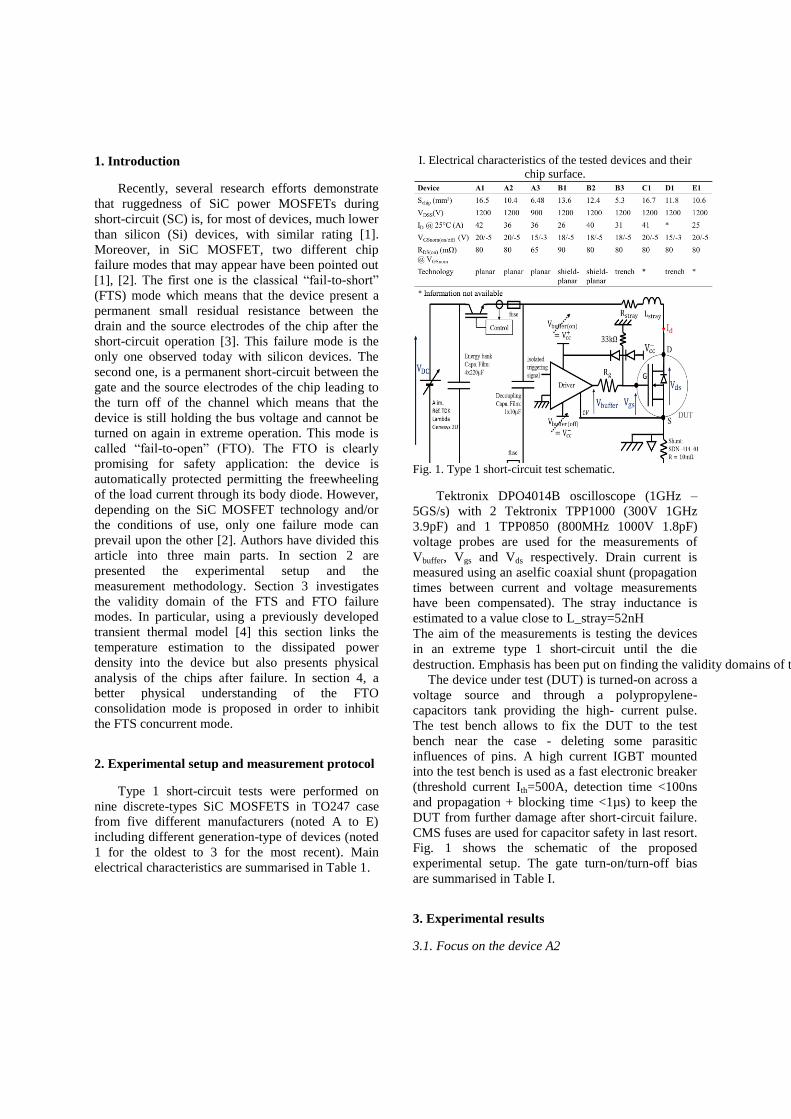
Fig. 1. Type 1 short-circuit test schematic.
Tektronix DPO4014B oscilloscope (1GHz –
5GS/s) with 2 Tektronix TPP1000 (300V 1GHz
3.9pF) and 1 TPP0850 (800MHz 1000V 1.8pF)
voltage probes are used for the measurements of
Vbuffer, Vgs and Vds respectively. Drain current is
measured using an aselfic coaxial shunt (propagation
times between current and voltage measurements
have been compensated). The stray inductance is
estimated to a value close to L_stray=52nH
The aim of the measurements is testing the devices
in an extreme type 1 short-circuit until the die
destruction. Emphasis has been put on finding the validity domains of the devices failure modes. In these objectives, destructive tests have been performed by slowly increasing the power density dissipated by the chip by incrementing drain-source voltage ( ) (0V– 600V).
The device under test (DUT) is turned-on across a
voltage source and through a polypropylene-
capacitors tank providing the high- current pulse. The test bench allows to fix the DUT to the test
bench near the case - deleting some parasitic
influences of pins. A high current IGBT mounted
into the test bench is used as a fast electronic breaker
(threshold current Ith=500A, detection time <100ns
and propagation + blocking time <1µs) to keep the
DUT from further damage after short-circuit failure.
CMS fuses are used for capacitor safety in last resort.
Fig. 1 shows the schematic of the proposed
experimental setup. The gate turn-on/turn-off bias
are summarised in Table I.
3. Experimental results
3.1. Focus on the device A2
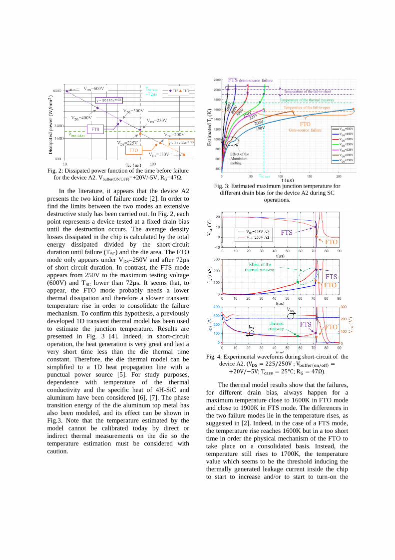
Fig. 2: Dissipated power function of the time before failure
for the device A2. Vbuffer(ON/OFF)=+20V/-5V, RG=47Ω.
In the literature, it appears that the device A2
presents the two kind of failure mode [2]. In order to
find the limits between the two modes an extensive
destructive study has been carried out. In Fig. 2, each
point represents a device tested at a fixed drain bias
until the destruction occurs. The average density
losses dissipated in the chip is calculated by the total
energy dissipated divided by the short-circuit
duration until failure (TSC) and the die area. The FTO
mode only appears under VDS=250V and after 72µs
of short-circuit duration. In contrast, the FTS mode
appears from 250V to the maximum testing voltage
(600V) and TSC lower than 72µs. It seems that, to
appear, the FTO mode probably needs a lower
thermal dissipation and therefore a slower transient
temperature rise in order to consolidate the failure
mechanism. To confirm this hypothesis, a previously
developed 1D transient thermal model has been used
to estimate the junction temperature. Results are
presented in Fig. 3 [4]. Indeed, in short-circuit
operation, the heat generation is very great and last a
very short time less than the die thermal time
constant. Therefore, the die thermal model can be
simplified to a 1D heat propagation line with a
punctual power source [5]. For study purposes,
dependence with temperature of the thermal
conductivity and the specific heat of 4H-SiC and
aluminum have been considered [6], [7]. The phase
transition energy of the die aluminum top metal has
also been modeled, and its effect can be shown in
Fig.3. Note that the temperature estimated by the
model cannot be calibrated today by direct or
indirect thermal measurements on the die so the
temperature estimation must be considered with
caution.
Fig. 3: Estimated maximum junction temperature for
different drain bias for the device A2 during SC
operations.
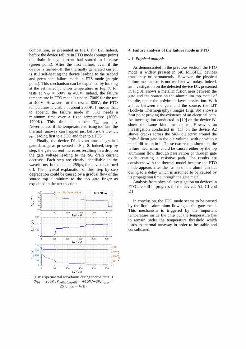
Fig. 4: Experimental waveforms during short-circuit of the
device A2. ( ;
; ; ).
The thermal model results show that the failures,
for different drain bias, always happen for a
maximum temperature close to 1600K in FTO mode
and close to 1900K in FTS mode. The differences in
the two failure modes lie in the temperature rises, as
suggested in [2]. Indeed, in the case of a FTS mode,
the temperature rise reaches 1600K but in a too short
time in order the physical mechanism of the FTO to
take place on a consolidated basis. Instead, the
temperature still rises to 1700K, the temperature
value which seems to be the threshold inducing the
thermally generated leakage current inside the chip
to start to increase and/or to start to turn-on the
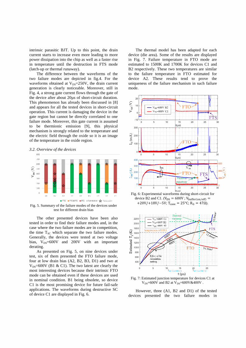
intrinsic parasitic BJT. Up to this point, the drain
current starts to increase even more leading to more
power dissipation into the chip as well as a faster rise
in temperature until the destruction in FTS mode
(latch-up or thermal runaway).
The difference between the waveforms of the
two failure modes are depicted in fig.4. For the
waveforms obtained at VDS=250V, the drain current
generation is clearly noticeable. Moreover, still in
Fig. 4, a strong gate current flows through the gate of
the device after about 20µs of short-circuit duration.
This phenomenon has already been discussed in [8]
and appears for all the tested devices in short-circuit
operation. This current is damaging the device in the
gate region but cannot be directly correlated to one
failure mode. Moreover, this gate current is assumed
to be thermionic emission [9], this physical
mechanism is strongly related to the temperature and
the electric field through the oxide so it is an image
of the temperature in the oxide region.
3.2. Overview of the devices
Fig. 5. Summary of the failure modes of the devices under
test for different drain bias
The other presented devices have been also
tested in order to find their failure modes and, in the
case where the two failure modes are in competition,
the time TSC which separate the two failure modes.
Generally, the devices were tested at two voltage
bias, VDS=600V and 200V with an important
derating.
As presented on Fig. 5, on nine devices under
test, six of them presented the FTO failure mode,
four at low drain bias (A2, B2, B3, D1) and two at
VDS=600V (B1 & C1). The two latest are clearly the
most interesting devices because their intrinsic FTO
mode can be obtained even if these devices are used
in nominal condition. B1 being obsolete, so device
C1 is the most promising device for future fail-safe
applications. The waveforms during destructive SC
of device C1 are displayed in Fig. 6.
The thermal model has been adapted for each
device (die area). Some of the results are displayed
in Fig. 7. Failure temperature in FTO mode are
estimated to 1500K and 1700K for devices C1 and
B2 respectively. These two temperatures are similar
to the failure temperature in FTO estimated for
device A2. These results tend to prove the
uniqueness of the failure mechanism in such failure
mode.
Fig. 6: Experimental waveforms during short-circuit for
device B2 and C1. ( ;
; ; ).
Fig. 7: Estimated junction temperature for devices C1 at
VDS=600V and B2 at VDS=600V&400V .
However, three (A1, B2 and D1) of the tested
devices presented the two failure modes in
competition, as presented in Fig 6 for B2. Indeed,
before the device failure in FTO mode (orange point)
the drain leakage current had started to increase
(green point). After the first failure, even if the
device is turned-off, the thermally generated current
is still self-heating the device leading to the second
and permanent failure mode in FTS mode (purple
point). This mechanism can be explained by looking
at the estimated junction temperature in Fig. 7, for
tests at VDS = 600V & 400V. Indeed, the failure
temperature in FTO mode is under 1700K for the test
at 400V. However, for the test at 600V, the FTO
temperature is visible at about 2000K. It means that,
to append, the failure mode in FTO needs a
minimum time over a fixed temperature (1600-
1700K). This time is named TSC limit FTO.
Nevertheless, if the temperature is rising too fast, the
thermal runaway can happen just before the TSC limit
FTO leading first to a FTO and then to a FTS.
Finally, the device D1 has an unusual gradual
gate damage as presented in Fig. 8. Indeed, step by
step, the gate current increases resulting in a drop on
the gate voltage leading to the SC drain current
decrease. Each step are clearly identifiable in the
waveforms. In the end, at 255µs, the device is turned
off. The physical explanation of this, step by step
degradation could be caused by a gradual flow of the
source top aluminium to the top gate finger as
explained in the next section.
Fig. 8: Experimental waveforms during short-circuit D1.
( ; ;
; ).
4. Failure analysis of the failure mode in FTO
4.1. Physical analysis
As demonstrated in the previous section, the FTO
mode is widely present in SiC MOSFET devices
transiently or permanently. However, the physical
failure mechanism is not well known today. Indeed,
an investigation on the defected device D1, presented
in Fig.8a, shows a metallic fusion area between the
gate and the source on the aluminium top metal of
the die, under the polyimide layer passivation. With
a bias between the gate and the source, the LIT
(Lock-In Thermography) images (Fig. 9b) shows a
heat point proving the existence of an electrical path.
An investigation conducted in [10] on the device B1
show the same kind mechanism. However, an
investigation conducted in [11] on the device A2
shows cracks across the SiO2 dielectric around the
Poly-Silicon gate in the die volume, with or without
metal diffusion in it. These two results show that the
failure mechanism could be caused either by the top
aluminum flow through passivation or through gate
oxide creating a resistive path. The results are
consistent with the thermal model because the FTO
mode appears after the fusion of the aluminum but
owing to a delay which is assumed to be caused by
its propagation time through the gate metal.
Analysis from physical investigation on devices in
FTO are still in progress for the devices A2, C1 and
D1.
In conclusion, the FTO mode seems to be caused
by the liquid aluminium flowing to the gate metal.
This mechanism is triggered by the important
temperature inside the chip but the temperature has
to remain under the temperature threshold which
leads to thermal runaway in order to be stable and
consolidated.
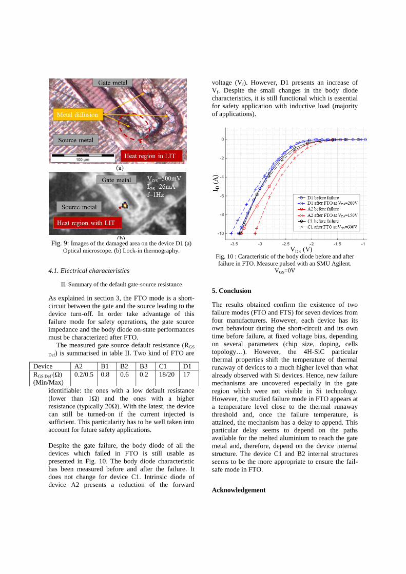
Fig. 9: Images of the damaged area on the device D1 (a)
Optical microscope. (b) Lock-in thermography.
4.1. Electrical characteristics
II. Summary of the default gate-source resistance
As explained in section 3, the FTO mode is a short-
circuit between the gate and the source leading to the
device turn-off. In order take advantage of this
failure mode for safety operations, the gate source
impedance and the body diode on-state performances
must be characterized after FTO.
The measured gate source default resistance (RGS
Def) is summarised in table II. Two kind of FTO are
identifiable: the ones with a low default resistance
(lower than 1Ω) and the ones with a higher
resistance (typically 20Ω). With the latest, the device
can still be turned-on if the current injected is
sufficient. This particularity has to be well taken into
account for future safety applications.
Despite the gate failure, the body diode of all the
devices which failed in FTO is still usable as
presented in Fig. 10. The body diode characteristic
has been measured before and after the failure. It
does not change for device C1. Intrinsic diode of
device A2 presents a reduction of the forward
voltage (Vf). However, D1 presents an increase of
Vf. Despite the small changes in the body diode
characteristics, it is still functional which is essential
for safety application with inductive load (majority
of applications).
Fig. 10 : Caracteristic of the body diode before and after
failure in FTO. Measure pulsed with an SMU Agilent.
VGS=0V
5. Conclusion
The results obtained confirm the existence of two
failure modes (FTO and FTS) for seven devices from
four manufacturers. However, each device has its
own behaviour during the short-circuit and its own
time before failure, at fixed voltage bias, depending
on several parameters (chip size, doping, cells
topology…). However, the 4H-SiC particular
thermal properties shift the temperature of thermal
runaway of devices to a much higher level than what
already observed with Si devices. Hence, new failure
mechanisms are uncovered especially in the gate
region which were not visible in Si technology.
However, the studied failure mode in FTO appears at
a temperature level close to the thermal runaway
threshold and, once the failure temperature, is
attained, the mechanism has a delay to append. This
particular delay seems to depend on the paths
available for the melted aluminium to reach the gate
metal and, therefore, depend on the device internal
structure. The device C1 and B2 internal structures
seems to be the more appropriate to ensure the fail-
safe mode in FTO.
Acknowledgement
Device A2 B1 B2 B3 C1 D1
RGS Def (Ω)
(Min/Max)
0.2/0.5 0.8 0.6 0.2 18/20 17
This research work received financial support from
the French National Research Agency (ANR).
Project name: HIT-TEMS managed by CNAM Paris
and Satie lab.
References
[1]C. Chen et al., Microelectron. Reliab., vol. 55, no. 9–10, pp.
1708–1713, 2015.
[2]G. Romano et al., IEEE J. Emerg. Sel. Top. Power Electron.,
vol. 4, no. 3, pp. 978–987, 2016.
[3]Z. Dou, Thesis, Toulouse, INPT, 2011.
[4]F. Boige et al., ElectrIMACS, May 2017.
[5]S. Clemente, IEEE Trans. Power Electron., vol. 8, no. 4, pp. 337–341, 1993.
[6]J. E. Hatch, Aluminum: Properties and Physical Metallurgy.
ASM International, 1984.
[7]L. L. Snead et al., J. Nucl. Mater., vol. 371, no. 1, pp. 329–
377, Sep. 2007.
[8]F. Boige et al., Microelectron. Reliab., vol. 76–77, no.
Supplement C, pp. 532–538, Sep. 2017.
[9]F.-C. Chiu, Advances in Materials Science and Engineering,
vol. 2014, Article ID 578168 [10]D. Othman, Thesis, Paris Saclay, 2015.
[11]F. Boige et al., Microelectron. Reliab., vol. 76–77, no.
Supplement C, pp. 500–506, Sep. 2017.