Embed Size (px)
Citation preview
NPL LeadNPL Lead--Free Master Classes 2003Free Master Classes 2003
Visit NPL www.Visit NPL www.nplnpl.co..co.ukuk//eiei
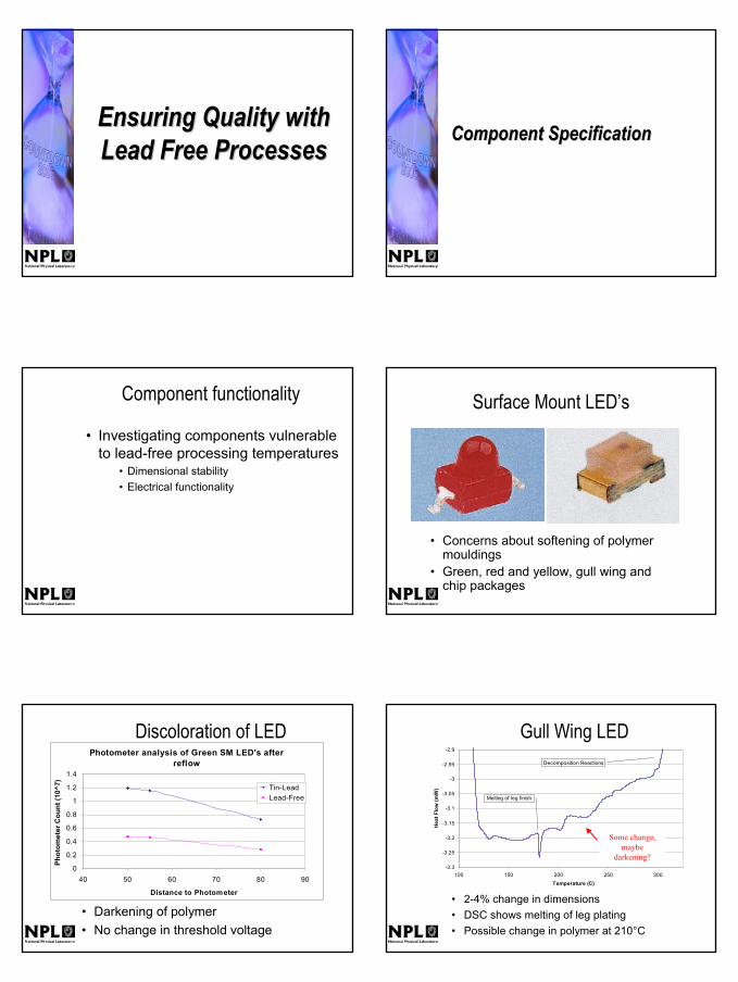
Ensuring Quality with Ensuring Quality with Lead Free ProcessesLead Free Processes Component SpecificationComponent Specification
Component functionality
• Investigating components vulnerable to lead-free processing temperatures
• Dimensional stability• Electrical functionality
Surface Mount LED’s
• Concerns about softening of polymer mouldings
• Green, red and yellow, gull wing and chip packages
Discoloration of LED
• Darkening of polymer• No change in threshold voltage
Photometer analysis of Green SM LED's after reflow
0
0.2
0.4
0.6
0.8
1
1.2
1.4
40 50 60 70 80 90
Distance to Photometer
Phot
omet
er C
ount
(10^
7) Tin-LeadLead-Free
Gull Wing LED
• 2-4% change in dimensions• DSC shows melting of leg plating• Possible change in polymer at 210°C
-3.3
-3.25
-3.2
-3.15
-3.1
-3.05
-3
-2.95
-2.9
100 150 200 250 300Temperature (C)
Hea
t Flo
w (m
W)
Melting of leg finish
Decomposition Reactions
Some change, maybe
darkening?
NPL LeadNPL Lead--Free Master Classes 2003Free Master Classes 2003
Visit NPL www.Visit NPL www.nplnpl.co..co.ukuk//eiei
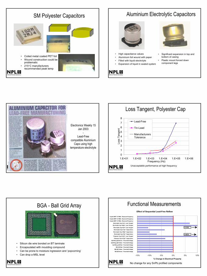
SM Polyester Capacitors
• Coiled metal coated PET foil• Wound construction could be
problematic• 215°C manufacturers
recommended peak temp
Aluminium Electrolytic Capacitors
• High capacitance values• Aluminium foil wound with paper• Filled with liquid electrolyte• Expansion of liquid in sealed system
• Significant expansion in top and bottom of casing
• Plastic mount forced down component legs
Electronics Weekly 15 Jan 2003
-Lead-Free
compatible Aluminium Caps using high
temperature electrolyte
Loss Tangent, Polyester Cap
Unacceptable performance at high frequency
0
1
2
3
4
5
6
7
8
1.E+01 1.E+02 1.E+03 1.E+04 1.E+05 1.E+06Frequency (Hz)
Loss
Tan
gent
Lead-Free
Tin-Lead
ManufacturersTolerance
BGA - Ball Grid Array
• Silicon die wire bonded on BT laminate• Encapsulated with moulding compound• Can be prone to moisture ingression and ‘popcorning’• Can drop a MSL level
Functional MeasurementsEffect of Sequential Lead-Free Reflow
-15% -10% -5% 0% 5% 10%
SM LED Green - Threshold Voltage
SM LED Yellow - Threshold Voltage
SM LED Red - Threshold Voltage
Gull Wing LED Red - Threshold Voltage
Gull Wing LED Yellow - Threshold Voltage
Gull Wing LED Green - Threshold Voltage
Polyester Cap 0.47µF - Capacitance
Polyester Cap 0.47µF - Loss Tangent
Electrolytic Cap 47µF - Capacitance
Electrolytic Cap 100µF - Capacitance
Electrolytic Cap 4.7µF - Capacitance
Electrolytic Cap 47µF - Loss Tangent
Electrolytic Cap 100µF - Loss Tangent
Electrolytic Cap 4.7µF - Loss Tangent
Crystal SMT 14.7MHz - Resonant Frequency
Crystal SMT 14.7MHz - Resonant Frequency
Crystal SMT 14.7MHz - Resonant Frequency
% Change in Electrical Property
+119%
+182%
No change for any SnPb profiled components
NPL LeadNPL Lead--Free Master Classes 2003Free Master Classes 2003
Visit NPL www.Visit NPL www.nplnpl.co..co.ukuk//eiei
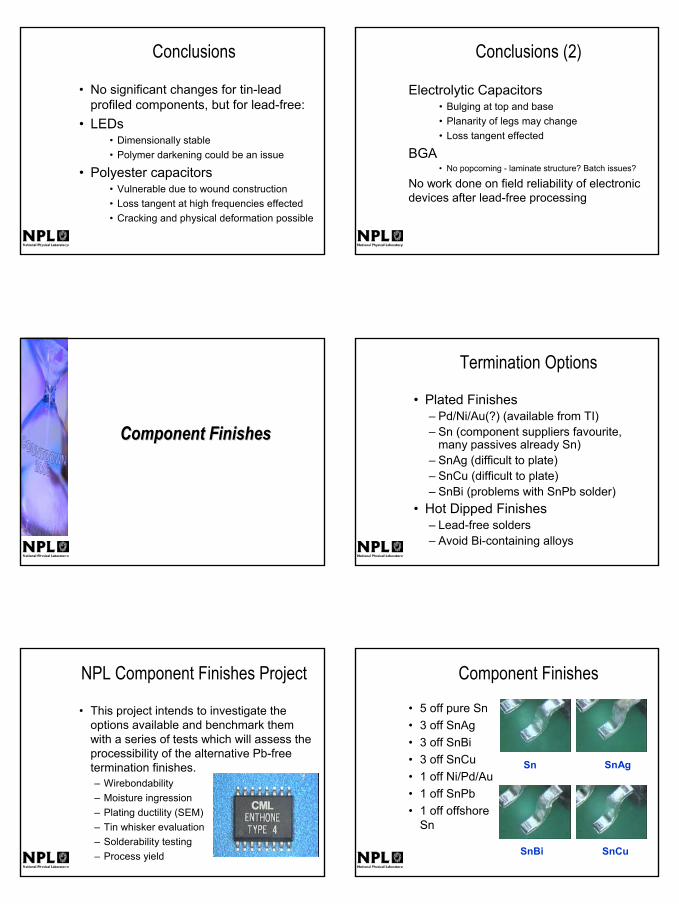
Conclusions
• No significant changes for tin-lead profiled components, but for lead-free:
• LEDs• Dimensionally stable• Polymer darkening could be an issue
• Polyester capacitors• Vulnerable due to wound construction• Loss tangent at high frequencies effected• Cracking and physical deformation possible
Conclusions (2)
Electrolytic Capacitors• Bulging at top and base• Planarity of legs may change• Loss tangent effected
BGA• No popcorning - laminate structure? Batch issues?
No work done on field reliability of electronic devices after lead-free processing
Component FinishesComponent Finishes
Termination Options
• Plated Finishes– Pd/Ni/Au(?) (available from TI)– Sn (component suppliers favourite,
many passives already Sn)– SnAg (difficult to plate)– SnCu (difficult to plate)– SnBi (problems with SnPb solder)
• Hot Dipped Finishes– Lead-free solders– Avoid Bi-containing alloys
NPL Component Finishes Project
• This project intends to investigate the options available and benchmark them with a series of tests which will assess the processibility of the alternative Pb-free termination finishes.– Wirebondability– Moisture ingression– Plating ductility (SEM)– Tin whisker evaluation– Solderability testing– Process yield
Component Finishes
• 5 off pure Sn• 3 off SnAg• 3 off SnBi• 3 off SnCu• 1 off Ni/Pd/Au • 1 off SnPb• 1 off offshore
Sn
Sn SnAg
SnBi SnCu
NPL LeadNPL Lead--Free Master Classes 2003Free Master Classes 2003
Visit NPL www.Visit NPL www.nplnpl.co..co.ukuk//eiei
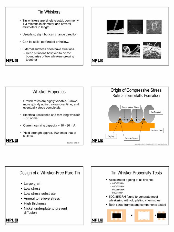
Tin Whiskers• Tin whiskers are single crystal, commonly
1-3 microns in diameter and several millimeters in length.
• Usually straight but can change direction
• Can be solid, perforated or hollow.
• External surfaces often have striations.– Deep striations believed to be the
boundaries of two whiskers growing together
• Growth rates are highly variable. Grows more quickly at first, slows over time, and eventually stops completely.
• Electrical resistance of 3 mm long whisker ~ 50 ohms.
• Current carrying capacity ~ 10 - 30 mA.
• Yield strength approx. 100 times that of bulk tin.
Whisker Properties
Source: Shipley
Origin of Compressive StressRole of Intermetallic Formation
Compressive Stress
Adapted from Lee B.Z, and Lee, D.N.1998 Acta Metallurgica
Cu Substrate
Sn Deposit
Cu6Sn5Tensile Stress
Design of a Whisker-Free Pure Tin
• Large grain• Low stress• Low stress substrate• Anneal to relieve stress• High thickness• Nickel underplate to prevent
diffusion
Tin Whisker Propensity Tests• Accelerated ageing of all finishes
– 85C/85%RH– 40C/90%RH– 50C/85%RH– 50C/lowRH
• 50C/85%RH found to generate most whiskering with old plating chemistries
• Both scrap frames and components tested
+
NPL LeadNPL Lead--Free Master Classes 2003Free Master Classes 2003
Visit NPL www.Visit NPL www.nplnpl.co..co.ukuk//eiei
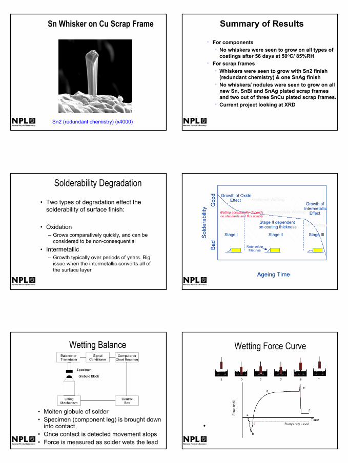
Sn Whisker on Cu Scrap Frame
Sn2 (redundant chemistry) (x4000)
Summary of Results
• For components• No whiskers were seen to grow on all types of
coatings after 56 days at 50oC/ 85%RH• For scrap frames
• Whiskers were seen to grow with Sn2 finish (redundant chemistry) & one SnAg finish
• No whiskers/ nodules were seen to grow on all new Sn, SnBi and SnAg plated scrap frames and two out of three SnCu plated scrap frames.
• Current project looking at XRD
Solderability Degradation
• Two types of degradation effect the solderability of surface finish:
• Oxidation– Grows comparatively quickly, and can be
considered to be non-consequential• Intermetallic
– Growth typically over periods of years. Big issue when the intermetallic converts all of the surface layer
Ageing Time
Bad
Goo
dSo
lder
abilit
y
Stage I Stage II Stage III
Growth of OxideEffect
Growth ofIntermetallic
Effect
Stage II dependenton coating thickness
Intermediate Wetting
Non Wetting
Preferred Wetting
Note solderfillet rise
Wetting acceptability depends on standards and flux activity
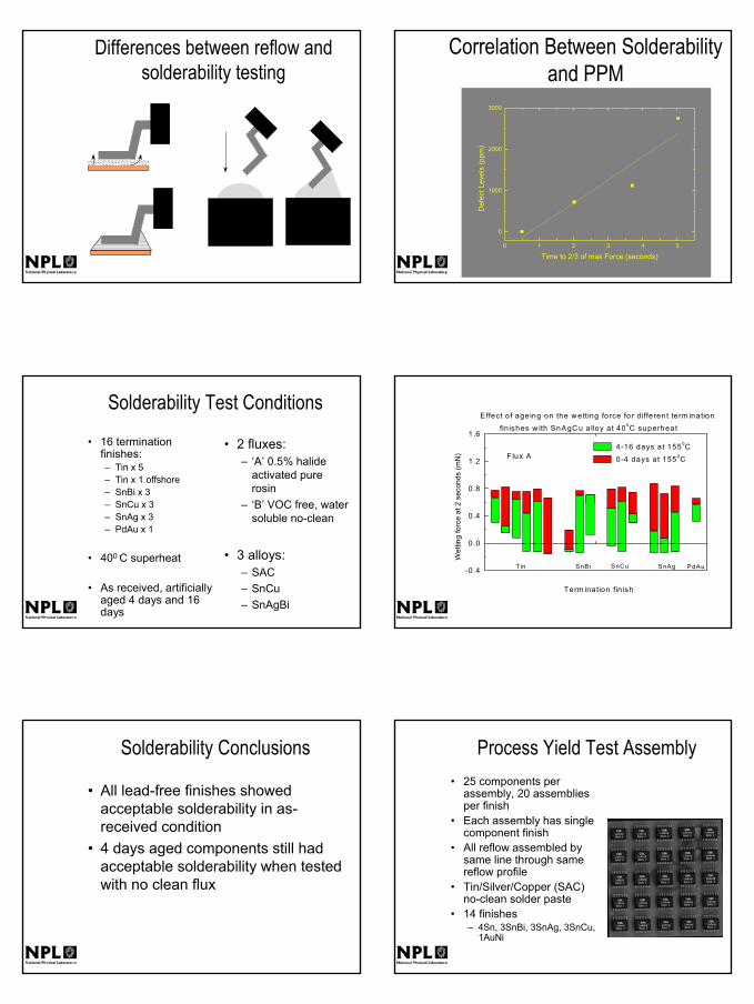
Wetting Balance
• Molten globule of solder• Specimen (component leg) is brought down
into contact• Once contact is detected movement stops• Force is measured as solder wets the lead
Wetting Force Curve
• Investigating component
NPL LeadNPL Lead--Free Master Classes 2003Free Master Classes 2003
Visit NPL www.Visit NPL www.nplnpl.co..co.ukuk//eiei
Differences between reflow and solderability testing
Correlation Between Solderability and PPM
0 1 2 3 4 5
0
1000
2000
3000
Def
ect L
evel
s (p
pm)
Time to 2/3 of max Force (seconds)
Solderability Test Conditions
• 16 termination finishes:– Tin x 5– Tin x 1 offshore– SnBi x 3– SnCu x 3– SnAg x 3– PdAu x 1
• 400 C superheat
• As received, artificially aged 4 days and 16 days
• 2 fluxes:– ‘A’ 0.5% halide
activated pure rosin
– ‘B’ VOC free, water soluble no-clean
• 3 alloys:– SAC– SnCu– SnAgBi
0 21
-0.4
0.0
0.4
0.8
1.2
1.6
E ffect o f age ing on the w etting force for d ifferent term ination fin ishes w ith SnAgC u a lloy a t 40 0C superheat
F lux A
PdAuSnAgSnCuSnBiT in
Wet
ting
forc
e at
2 s
econ
ds (m
N)
Term ination fin ish
4-16 days at 1550C 0-4 days at 155 0C
Solderability Conclusions
• All lead-free finishes showed acceptable solderability in as-received condition
• 4 days aged components still had acceptable solderability when tested with no clean flux
Process Yield Test Assembly• 25 components per
assembly, 20 assemblies per finish
• Each assembly has single component finish
• All reflow assembled by same line through same reflow profile
• Tin/Silver/Copper (SAC) no-clean solder paste
• 14 finishes– 4Sn, 3SnBi, 3SnAg, 3SnCu,
1AuNi
NPL LeadNPL Lead--Free Master Classes 2003Free Master Classes 2003
Visit NPL www.Visit NPL www.nplnpl.co..co.ukuk//eiei
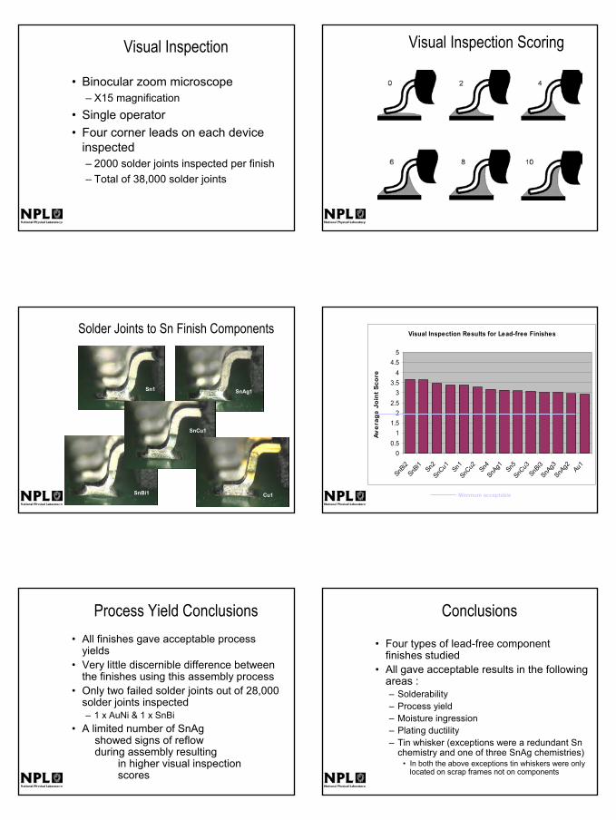
Visual Inspection
• Binocular zoom microscope– X15 magnification
• Single operator• Four corner leads on each device
inspected– 2000 solder joints inspected per finish– Total of 38,000 solder joints
Visual Inspection Scoring
Solder Joints to Sn Finish Components
Sn2
Sn1
Sn4 Sn5
SnAg1
SnBi1
SnCu1
Cu1
Visual Inspection Results for Lead-free Finishes
00.5
11.5
22.5
33.5
44.5
5
SnBi2
SnBi1
Sn2
SnCu1 Sn1
SnCu2 Sn4
SnAg1 Sn5
SnCu3
SnBi3
SnAg3
SnAg2 Au1
Aver
age
Join
t Sco
re
Minimum acceptable
Process Yield Conclusions• All finishes gave acceptable process
yields• Very little discernible difference between
the finishes using this assembly process• Only two failed solder joints out of 28,000
solder joints inspected– 1 x AuNi & 1 x SnBi
• A limited number of SnAg showed signs of reflow during assembly resulting
in higher visual inspection scores
Conclusions
• Four types of lead-free component finishes studied
• All gave acceptable results in the following areas :– Solderability– Process yield– Moisture ingression– Plating ductility– Tin whisker (exceptions were a redundant Sn
chemistry and one of three SnAg chemistries)• In both the above exceptions tin whiskers were only
located on scrap frames not on components
NPL LeadNPL Lead--Free Master Classes 2003Free Master Classes 2003
Visit NPL www.Visit NPL www.nplnpl.co..co.ukuk//eiei
Inspection RequirementsInspection Requirements
LF Inspection Standards
• IPC-A-610 has been reviewed for lead-free inspection
• Lead-Free Cookbook has examples• SAC joints
– Slightly duller surface– Copper halo more likely
• Re-education of inspectors
AOI and LF• NPL Study included the following defects:
– Missing components.– Misaligned components (x and y directions).– Wrong components (correct size but different
value).– Poor quality solder joints (insufficient or
excess solder).– Wrong polarity components.– Solder bridges (shorts).– Poor lead or component planarity including
tombstones (component on end) and components on edge.
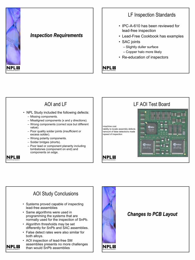
LF AOI Test Board
•machine cost•ability to locate assembly defects•amount of false detections made•speed of inspection
AOI Study Conclusions
• Systems proved capable of inspecting lead-free assemblies
• Same algorithms were used in programming the systems that are normally used for the inspection of SnPb.
• Algorithm thresholds may be set differently for SnPb and SAC assemblies.
• False detect rates were also similar for both alloys.
• AOI inspection of lead-free SM assemblies presents no more challenges than would SnPb assemblies
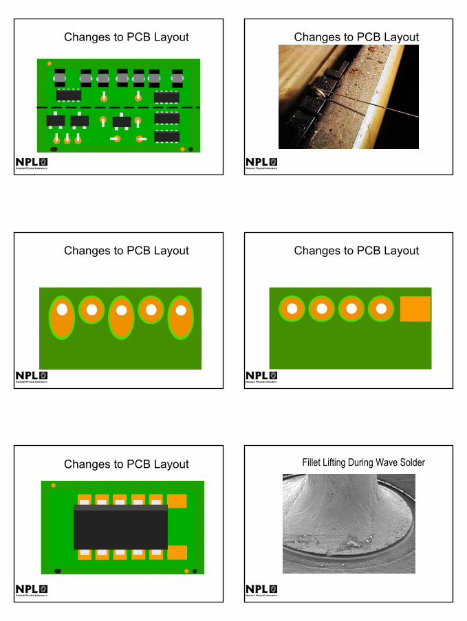
Changes to PCB LayoutChanges to PCB Layout
NPL LeadNPL Lead--Free Master Classes 2003Free Master Classes 2003
Visit NPL www.Visit NPL www.nplnpl.co..co.ukuk//eiei
Changes to PCB Layout Changes to PCB Layout
Changes to PCB Layout Changes to PCB Layout
Changes to PCB Layout Fillet Lifting During Wave Solder
NPL LeadNPL Lead--Free Master Classes 2003Free Master Classes 2003
Visit NPL www.Visit NPL www.nplnpl.co..co.ukuk//eiei
Pad Lifting During Wave Solder
Wave Soldering IssuesWave Soldering Issues
Lead-Free Wave Soldering Lead-Free Wave Soldering
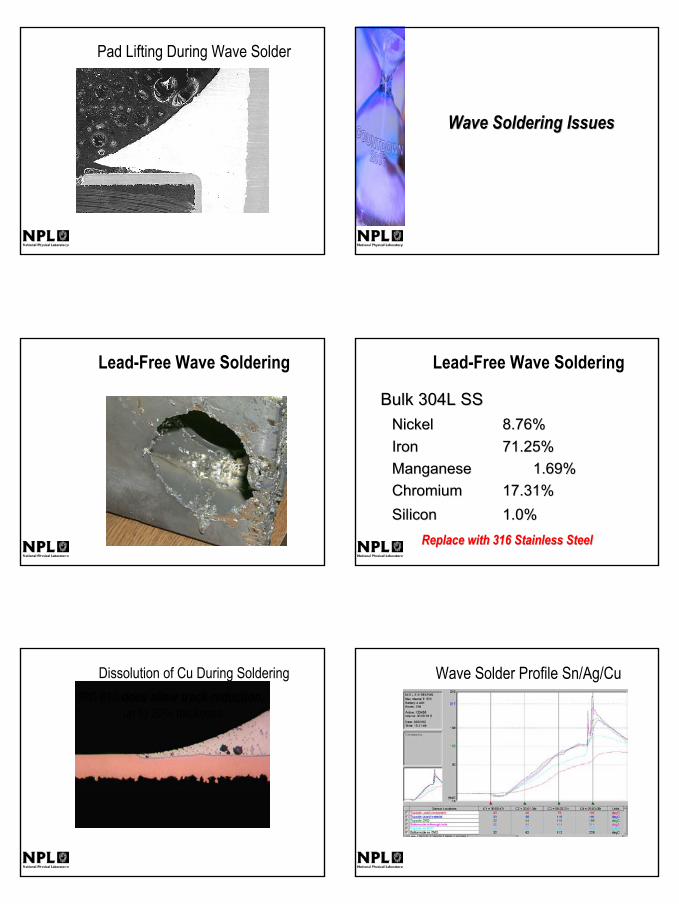
Bulk 304L SSBulk 304L SSNickel Nickel 8.76%8.76%Iron Iron 71.25%71.25%Manganese Manganese 1.69%1.69%ChromiumChromium 17.31%17.31%SiliconSilicon 1.0%1.0%
Replace with 316 Stainless SteelReplace with 316 Stainless Steel
Dissolution of Cu During SolderingIPC 610 does allow track reduction,
up to 20% thickness
Wave Solder Profile Sn/Ag/Cu
NPL LeadNPL Lead--Free Master Classes 2003Free Master Classes 2003
Visit NPL www.Visit NPL www.nplnpl.co..co.ukuk//eiei
Wave Solder Bath Analysis Wave Solder Bath Analysis
Reflow Soldering IssuesReflow Soldering Issues
BW Reflow Deluxe 7
Reflow Soldering
Temperature Profiling
0123456789
10
Solder Al Tape Kapton Tape Epoxy
AverageRangeStan Dev
NPL LeadNPL Lead--Free Master Classes 2003Free Master Classes 2003
Visit NPL www.Visit NPL www.nplnpl.co..co.ukuk//eiei
NEC Lead-Free Assembly Thank you for your attentionThank you for your attention
www.npl.co.uk/npl/ei