Embed Size (px)
Citation preview

Enterprise and Datacenter SSD Formfactor Connector Specification 0.9 Draft
1
Enterprise and Datacenter
SSD Form Factor
Connector Specification
Revision 0.9 Draft
August 2, 2017
Enterprise and Datacenter SSD Form Factor Working Group
Enterprise and Datacenter SSD Formfactor Connector Specification 0.9 Draft
2
INTELLECTUAL PROPERTY DISCLAIMER THIS DRAFT VERSION OF THE SPECIFICATION IS PROVIDED “AS IS” WITH NO WARRANTIES WHATSOEVER INCLUDING ANY WARRANTY OF MERCHANTABILITY, FITNESS FOR ANY PARTICULAR PURPOSE, OR ANY WARRANTY OTHERWISE ARISING OUT OF ANY PROPOSAL, SPECIFICATION, OR SAMPLE.
THIS DRAFT VERSION OF THE SPECIFICATION IS PROVIDED FOR INFORMATIONAL PURPOSES ONLY AND NO LICENSE, EXPRESS OR IMPLIED, BY ESTOPPEL OR OTHERWISE, TO ANY INTELLECTUAL PROPERTY RIGHTS IS GRANTED OR INTENDED HEREBY.
THE ENTERPRISE AND DATACENTER SSD FORM FACTOR WORKGROUP AND EACH INDIVIDUAL MEMBER THEREOF DISCLAIMS ALL LIABILITY, INCLUDING LIABILITY FOR INFRINGEMENT OF PROPRIETARY RIGHTS, RELATING TO IMPLEMENTATION OF INFORMATION IN THIS SPECIFICATION. THE ENTERPRISE AND DATACENTER SSD FORM FACTOR WORKGROUP DOES NOT WARRANT OR REPRESENT THAT SUCH IMPLEMENTATION(S) WILL NOT INFRINGE SUCH RIGHTS.

Enterprise and Datacenter SSD Formfactor Connector Specification 0.9 Draft
3
Revision History
Rev History Date
0.9 Draft spec 8/2/2017

Enterprise and Datacenter SSD Formfactor Connector Specification 0.9 Draft
4
Table of Contents
1 INTRODUCTION........................................................................................................... 5
1.1 Overview .................................................................................................................................................... 5
1.2 Goals ......................................................................................................................................................... 5
1.3 Scope ......................................................................................................................................................... 5
1.4 Outside of Scope ....................................................................................................................................... 5
1.5 Features..................................................................................................................................................... 5
1.6 Terms and Definitions ................................................................................................................................ 5
1.7 Keywords ................................................................................................................................................... 6
1.8 Specification References ........................................................................................................................... 6
2 SIGNAL LIST .............................................................................................................. 7
2.1 Power and Grounds ................................................................................................................................... 8
2.2 PCIe Signals .............................................................................................................................................. 8
2.3 Side Band Signals ................................................................................................................................... 10
2.4 Connector pinout definitions .................................................................................................................... 11
3 CARD EDGE AND CONNECTOR SPECIFICATION .............................................................. 16

Enterprise and Datacenter SSD Formfactor Connector Specification 0.9 Draft
5
1 Introduction
1.1 Overview
The following specification defines the terminology, electrical, and mechanical requirements for a Card edge plug and connector receptacle that is defined for use in Enterprise and Datacenter applications supporting PCIe-based Solid-State Storage Devices (SSDs).
1.2 Goals
The following goals were established when defining this specification.
High-Level Tenets:
PCIe is the interface for the specification.
Cost optimal: Avoid the use of exotic (and costly) approaches
Thermal/Power Efficient
1.3 Scope
This specification defines the following:
The pin list and pin placement
Function of the pins
1.4 Outside of Scope
The implementation or use of other published specifications referred to in this specification, even if required for compliance with the specification, are outside the scope of this specification (for example, PCI Express).
How the connector connects physically and electrically to the host is outside of scope. There are informative examples to show possible implementations
1.5 Features
PCIe support for today and future specifications
o Supports 3.1a specification (up to 8GTs signaling) with no restrictions to support 16GT/s and 32GT/s.
o Single port operation: One (1), x4 or x8 or x16 PCIe port supported
o Dual port: Two (2) x2 or two (2) x4 or two (2) x8 PCIe ports supported
3 connector types
o A 56 pin receptacle supporting Four (4) Tx and Rx PCIe lanes.
o A 84 pin receptacle supporting Eight (8) Tx and Rx PCIe lanes.
o A 140 pin receptacle supporting Sixteen (16) Tx and Rx PCIe lanes.
Hot-plug Support
1.6 Terms and Definitions

Enterprise and Datacenter SSD Formfactor Connector Specification 0.9 Draft
6
1.6.1 Host: Refers to the interface source or master
1.6.2 Device: Refers to the interface slave
1.6.3 Card: Refers to the device plugged into a connector
1.6.4 NVM: Acronym for Non-Volatile Memory
1.6.5 SSD: Acronym for Solid State Drive
1.6.6 SRIS: Acronym for Separate Reference clock Independent Spread spectrum clocking. This is a PCI Express feature that allows independent reference clocks for host and device. In this implementation, the host does not need to provide the reference clock. Each Independent source supports Spread Spectrum Clocking (SSC).
1.6.7 SRNS: Acronym for Separate Reference clock with No Spread spectrum clocking. This is a PCI Express feature that allows independent reference clocks for host and device. In this implementation, the host does not need to provide the reference clock. Spread Spectrum Clocking (SSC) is not supported by either source.
1.7 Keywords
1.7.1 Mandatory: Indicates items to be implemented as defined by this specification
1.7.2 May: Indicates flexibility of choice with no implied preference
1.7.3 Optional: Describes features that are not required by this specification. However, if any optional feature defined by the specification is implemented, the feature shall be implemented in the way defined by the specification.
1.7.4 Reserved: Refers to bits, bytes, words, fields, and opcode values that are set-aside for future standardization. Their use and interpretation may be specified by future extensions to this or other specifications. A reserved bit, byte, word, field, or register shall be cleared to zero, or in accordance with a future extension to this specification. The recipient is not required to check reserved bits, bytes, words, or fields. Receipt of reserved coded values in defined fields in commands shall be reported as an error. Writing a reserved coded value into a controller register field produces undefined results.
1.7.5 Shall: Indicates a mandatory requirement. Designers are required to implement all such mandatory requirements to ensure interoperability with other products that conform to the specification.
1.7.6 Should: Indicates flexibility of choice with a strongly preferred alternative. Equivalent to the phrase “it is recommended”.
1.8 Specification References
PCI Express® (PCIe) Specifications are available from http://www.pcisig.com.
PCI Express Base Specification, revision 3.1a
PCI Express Mini Card Electromechanical Specification Revision 2.1
System Management Bus (SMBus) Specification, Version 2.0, August 3, 2000, available from http://smbus.org
SNIA SFF-TA-1002 Protocol Agnostic Multi-Lane High Speed Connector specification available at http://www.snia.org.

Enterprise and Datacenter SSD Formfactor Connector Specification 0.9 Draft
7
2 Signal List
This chapter covers the signal summary, definitions, and signal placement for the EDSFF connectors. All signals listed are looking from the device and are mandatory unless otherwise specified.
Table 1: EDSFF Connector pin list
Interface Signal Name Card I/O
Function
Power and Grounds
12 V I +12 V source
3.3 Vaux I +3.3 V Source
GND I Return current path
PCIe
PERp0, PERn0, PETp0, PETn0
I/O
PCIe TX/RX Differential signals defined by the PCI Express Card Electromechanical Specification. PERp/n[0..3] and PETp/n[0..3] are supported in both the x4 and x8 connectors. PERp/n[4..7] and PETp/n[4..7] are supported only with the x8 connector. PERp/n[8..15] and PETp/n[8..15] are supported only with the x16 connector.
PERp1, PERn1, PETp1, PETn1
PERp2, PERn2, PETp2, PETn2
PERp3, PERn3, PETp3, PETn3
PERp4, PERn4, PETp4, PETn4
PERp5, PERn5, PETp5, PETn5
PERp6, PERn6, PETp6, PETn6
PERp7, PERn7, PETp7, PETn7
PERp8, PERn8, PETp8, PETn8
PERp9, PERn9, PETp9, PETn9
PERp10, PERn10, PETp10, PETn10
PERp11, PERn11, PETp11, PETn11
PERp12, PERn12, PETp12, PETn12
PERp13, PERn13, PETp13, PETn13
PERp14, PERn14, PETp14, PETn14
PERp15, PERn15, PETp15, PETn15
REFCLKp0, REFCLKn0 I
PCIe Reference Clock signals (100 MHz) defined by the PCI Express Card Electromechanical Specification. Note: This reference clock is the common ref clock that shall be used with PCIe.
PERST0_n I PE-Reset is a functional reset to the card as defined as PERST# by the PCI Express Mini Card Electromechanical Specification.
REFCLKp1, REFCLKn1 I
PCIe Reference Clock signals (100 MHz) defined by the PCI Express Card Electromechanical Specification. This clock is for dual port mode only and will only be used if DualPortEn_n is low. Note: This reference clock is the common ref clock that shall be used with PCIe.
PERST1_n/CLKREQ_n I/O
PERST1_n: PE-Reset is a functional reset to the card as defined as PERST# by the PCI Express Mini Card Electromechanical Specification. If dual port mode is supported by the card, PERST1_n will only be used if DualPortEn_n is low. CLKREQ_n: Clock Request is a reference clock request signal as defined as CLKREQ# by the PCI Express Mini CEM Specification. It is only supported in single port mode. If CLKREQ_n is

Enterprise and Datacenter SSD Formfactor Connector Specification 0.9 Draft
8
supported by the card, the signal is Open Drain with a pull up on host. CLKREQ_n is active low and used by L1 PM Substates.
Sideband Signals
PRSNT0_n O Active low signal. This signal indicates to the host that the card is electrically attached.
PRSNT1_n O
PRSNT1_n: Active low signal. This signal is in the x8 connector as a 2nd presence signal to indicate to the host that the card is electrically attached.
PRSNT2_n O PRSNT2_n: Active low signal. This signal is in the x16 connector as a 3rd presence signal to indicate to the host that the card is electrically attached.
SMBCLK I SMBus Clock, Open Drain with pull-up on host.
SMBDATA I/O SMBus Data, Open Drain with pull-up on host.
SMBRST_n I Active low signal: SMBRST_n is a reset for the management interface. It is expected to operate independently of PERST[0..1]_n.
DualPortEn_n I Active low signal. This signal indicates if dual port mode is supported by the host.
LED/Activity I or O
LED: Active high input signal. This signal is used to pass the LED state from the host to the device. Activity: Active high output signal. This allows the device to provide status of data transfer to the host.
PWRDIS I Power Disable. Active high. This signal notifies the device to turn off all systems connected to 12 V power.
MFG I Manufacturing Mode for device. Host should not use/connect.
RFU Reserved for Future Use
2.1 Power and Grounds
The EDSFF connector supports a 12 V power source to power the majority of the card with a smaller 3.3 Vaux power source to provide power to manage sideband communication. Both rails are expected to be powered while the card is in the system.
2.2 PCIe Signals
2.2.1 High Speed Signals (PERp/n, PETp/n)
The PCIe interface supports a minimum of one (1) lane. A lane consists of an input and output differential pair. Refer to the PCI Express Base Specification for more details on the functional requirements of the interface signals.

Enterprise and Datacenter SSD Formfactor Connector Specification 0.9 Draft
9
PET on the card shall be connected to PER on the host. PER on the card shall be connected to PET on the host.
Lane polarity reversal shall be supported to simplify host and card PCB trace routing constraints.
Table 2 shows the connectivity in both single and dual port systems. Dual Port usage is indicated with DualPortEn_n assertion.
Table 2: PCIe lanes connectivity in single and dual port implementations
PCIe lanes x4 Single Port
(1 port x4) x4 Dual Port (2 ports x2)
X8 Single Port (1 port x8)
x8 Dual Port (2 ports x4)
x16 Single Port (1 port x16)
x16 Dual Port (2 ports x8)
PERp0, PERn0, PETp0, PETn0 Port A, lane 0 Port A, lane 0 Port A, lane 0 Port A, lane 0 Port A, lane 0 Port A, lane 0 PERp1, PERn1, PETp1, PETn1 Port A, lane 1 Port A, lane 1 Port A, lane 1 Port A, lane 1 Port A, lane 1 Port A, lane 1 PERp2, PERn2, PETp2, PETn2 Port A, lane 2 Port B, lane 0 Port A, lane 2 Port B, lane 0 Port A, lane 2 Port B, lane 0 PERp3, PERn3, PETp3, PETn3 Port A, lane 3 Port B, lane 1 Port A, lane 3 Port B, lane 1 Port A, lane 3 Port B, lane 1 PERp4, PERn4, PETp4, PETn4 No connect No connect Port A, lane 4 Port A, lane 2 Port A, lane 4 Port A, lane 2 PERp5, PERn5, PETp5, PETn5 No connect No connect Port A, lane 5 Port A, lane 3 Port A, lane 5 Port A, lane 3 PERp6, PERn6, PETp6, PETn6 No connect No connect Port A, lane 6 Port B, lane 2 Port A, lane 6 Port B, lane 2 PERp7, PERn7, PETp7, PETn7 No connect No connect Port A, lane 7 Port B, lane 3 Port A, lane 7 Port B, lane 3 PERp8, PERn8, PETp8, PETn8 No connect No connect No connect No connect Port A, lane 8 Port A, lane 4 PERp9, PERn9, PETp9, PETn9 No connect No connect No connect No connect Port A, lane 9 Port A, lane 5
PERp10, PERn10, PETp10, PETn10 No connect No connect No connect No connect Port A, lane 10 Port B, lane 4 PERp11, PERn11, PETp11, PETn11 No connect No connect No connect No connect Port A, lane 11 Port B, lane 5 PERp12, PERn12, PETp12, PETn12 No connect No connect No connect No connect Port A, lane12 Port A, lane 6 PERp13, PERn13, PETp13, PETn13 No connect No connect No connect No connect Port A, lane 13 Port A, lane 7 PERp14, PERn14, PETp14, PETn14 No connect No connect No connect No connect Port A, lane 14 Port B, lane 6 PERp15, PERn15, PETp15, PETn15 No connect No connect No connect No connect Port A, lane 15 Port B, lane 7
2.2.2 Reference Clock
The REFCLKp/REFCLKn signals are used to assist the synchronization of the device’s PCI Express interface timing circuits. Refer to the PCI Express Card Electromechanical Specification for more details on the functional and tolerance requirements for the reference clock signals.
There are two sets of clock pairs. In a single port implementation (indicated by DualPortEn_n de-asserted), only REFCLKp0 and REFCLKn0 are used. In a dual port system (indicated by DualPortEn_n asserted), REFCLKp0 and REFCLKn0 connects to Port A while REFCLKp1 and REFCLKn1 connects to port B.

Enterprise and Datacenter SSD Formfactor Connector Specification 0.9 Draft
10
If SRIS or SRNS is supported by both the system and the device then these signals may not be connected.
2.2.3 PERST_n
The PERST_n signal operates as a Link reset for PCI Express. Refer to the PCI Express Card Electromechanical Specification for more details on the functional requirements of the interface signals.
In a single port implementation (indicated by DualPortEn_n de-asserted), only PERST0_n is used. In this situation, PERST1_n is not used; however, the CLKREQ_n function can still be used. If neither function is supported by the host, the signal should be tied to ground.
In a dual port system (indicated by DualPortEn_n asserted), PERST0_n connects to Port A and PERST1_n connects to port B.
2.2.4 CLKREQ_n
The CLKREQ_n signal is used by the L1 PM Substates mechanism. In this case, CLKREQ_n can be asserted by either the system or the device to initiate an L1 exit. See the PCI Express Base Specification for details on the functional requirements for the CLKREQ_n signal when implementing L1 PM Substates.
If dualporten_n is asserted, CLKREQ_n shall not be used.
2.3 Side Band Signals
2.3.1 PRSNT[0..2]_n
The PRSNT_n signals are used to indicate physical presence of a card plugged into the connector. The x4 connector utilizes only one signal (PRSNT0_n). The x8 connector utilizes a second signal (PRSNT1_n). The x16 connector utilizes a third signal (PRSNT2_n).
2.3.2 SMBus Interface
The SMBus interface is intended as a side band management interface. SMBus is a two-wire interface through which various system component chips can communicate with each other and with rest of the system. It is based on I2C principles of operation. Refer to the SMBus Specification for details of the operation
The SMBCLK signal provides the clock signaling from the SMBus master to the SMBus slave device to be able to decode the data on the SMBDATA line.
The SMBDATA signal is used to transfer the data packets between the host and the device according to the SMBus protocol.
2.3.3 SMBRST_n
The SMBRST_n signal is intended to place the portion of the SSD that brings the management of the SSD back to an initial state without interrupting the PCIe link or losing NVMe controller data. Details of what is reset as well as the implementation on the device is not defined in this specification.
There are usages where the host may have SMBus connected to multiple devices. If the host holds SMBRST_n low, the device shall keep the SMBCLK and SMBDATA in a high impedance state and ignore any communication on SMBCLK and SMBDATA.

Enterprise and Datacenter SSD Formfactor Connector Specification 0.9 Draft
11
2.3.4 DualPortEn_n
The SSD can be configured by the host as a single port or dual port device using the DualPortEn_n signal. . See Table 3 for expected functionality.
Table 3: SSD configuration for single port vs. dual port.
System DualPortEn_n state x4 SSD x8 SSD X16 SSD
x4 De-asserted Single Port x4 Single Port x4 Single Port x4
Asserted Dual Port x2 Dual Port x2 Dual Port x2
x8 De-asserted Single Port x4 Single Port x8 Single Port x8
Asserted Dual Port x2 Dual Port x4 Dual Port x4
X16 De-asserted Single Port x4 Single Port x8 Single Port x16
Asserted Dual Port x2 Dual Port x4 Dual Port x8
2.3.5 LED/Activity
The LED signal is asserted by the host to drive an LED on the card. The host use of the LED signal is optional. Details of the usage of LED is beyond the scope of this specification.
The Activity signal is asserted by the card to indicate SSD activity. The host use of the Activity signal is optional. The blink patterns are beyond the scope of this specification.
To prevent contention, either LED or Activity will be supported but not both. It is up to the system implementation to set the correct function. The default function shall be LED which is an input to the device.
2.3.6 PWRDIS
The PWRDIS signal is asserted to tell the card to shut off power to all circuitry connected to the 12 V power supply.
2.3.7 MFG
The MFG signal is used for device manufacturing only. This signal shall be electrically no-connect on the host.
Post device manufacturing, the device manufacturer shall ensure that the pin is disabled.
2.3.8 RFU
Signals documented as RFU are reserved for future use. These pins shall be electrically no-connect on the host and the card. These pins are reserved for future assignment as a functional signal.
2.4 Connector pinout definitions
The following tables show the signal pinouts for the Card edge connector. These pinouts are shown from the card point of view.
Table 4 lists the pinout for the x4 connector
Table 5 lists the pinout for the x8 connector

Enterprise and Datacenter SSD Formfactor Connector Specification 0.9 Draft
12
Table 6 lists the pinout for the x16 connector
Table 4: EDSFF x4 card edge pinout
Pin Signal Signal Pin
A28 GND GND B28
A27 PETp3 PERp3 B27
A26 PETn3 PERn3 B26
A25 GND GND B25
A24 PETp2 PERp2 B24
A23 PETn2 PERn2 B23
A22 GND GND B22
A21 PETp1 PERp1 B21
A20 PETn1 PERn1 B20
A19 GND GND B19
A18 PETp0 PERp0 B18
A17 PETn0 PERn0 B17
A16 GND GND B16
A15 REFCLKp1 REFCLKp0 B15
A14 REFCLKn1 REFCLKn0 B14
A13 GND GND B13
A12 PRSNT0_n PWRDIS B12
A11 PERST1_n/CLKREQ_n 3.3 Vaux B11
A10 LED/Activity PERST0_n B10
A9 SMBRST_n DualPortEn_n B9
A8 SMBDAT RFU B8
A7 SMBCLK MFG B7
A6 GND 12 V B6
A5 GND 12 V B5
A4 GND 12 V B4
A3 GND 12 V B3
A2 GND 12 V B2
A1 GND 12 V B1
Table 5: EDSFF x8 card edge pinout
Pin Signal Signal Pin
A42 RFU PRSNT1_n B42
A41 GND GND B41

Enterprise and Datacenter SSD Formfactor Connector Specification 0.9 Draft
13
A40 PETp7 PERp7 B40
A39 PETn7 PERn7 B39
A38 GND GND B38
A37 PETp6 PERp6 B37
A36 PETn6 PERn6 B36
A35 GND GND B35
A34 PETp5 PERp5 B34
A33 PETn5 PERn5 B33
A32 GND GND B32
A31 PETp4 PERp4 B31
A30 PETn4 PERn4 B30
A29 GND GND B29
Key Key
A28 GND GND B28
A27 PETp3 PERp3 B27
A26 PETn3 PERn3 B26
A25 GND GND B25
A24 PETp2 PERp2 B24
A23 PETn2 PERn2 B23
A22 GND GND B22
A21 PETp1 PERp1 B21
A20 PETn1 PERn1 B20
A19 GND GND B19
A18 PETp0 PERp0 B18
A17 PETn0 PERn0 B17
A16 GND GND B16
A15 REFCLKp1 REFCLKp0 B15
A14 REFCLKn1 REFCLKn0 B14
A13 GND GND B13
A12 PRSNT0_n PWRDIS B12
A11 PERST1_n/CLKREQ_n 3.3 Vaux B11
A10 LED/Activity PERST0_n B10
A9 SMBRST_n DualPortEn_n B9
A8 SMBDAT RFU B8
A7 SMBCLK MFG B7
A6 GND 12 V B6
A5 GND 12 V B5
A4 GND 12 V B4
A3 GND 12 V B3
A2 GND 12 V B2

Enterprise and Datacenter SSD Formfactor Connector Specification 0.9 Draft
14
A1 GND 12 V B1
Table 6: EDSFF x16 card edge pinout
Pin Signal Signal Pin
A70 RFU PRSNT2_n B70
A69 RFU RFU B69
A68 RFU RFU B68
A67 GND GND B67
A66 PETp15 PERp15 B66
A65 PETn15 PERn15 B65
A64 GND GND B64
A63 PETp14 PERp14 B63
A62 PETn14 PERn14 B62
A61 GND GND B61
A60 PETp13 PERp13 B60
A59 PETn13 PERn13 B59
A58 GND GND B58
A57 PETp12 PERp12 B57
A56 PETn12 PERn12 B56
A55 GND GND B55
A54 PETp11 PERp11 B54
A53 PETn11 PERn11 B53
A52 GND GND B52
A51 PETp10 PERp10 B51
A50 PETn10 PERn10 B50
A49 GND GND B49
A48 PETp9 PERp9 B48
A47 PETn9 PERn9 B47
A46 GND GND B46
A45 PETp8 PERp8 B45
A44 PETn8 PERn8 B44
A43 GND GND B43
Key Key
A42 RFU PRSNT1_n B42
A41 GND GND B41
A40 PETp7 PERp7 B40
A39 PETn7 PERn7 B39
A38 GND GND B38
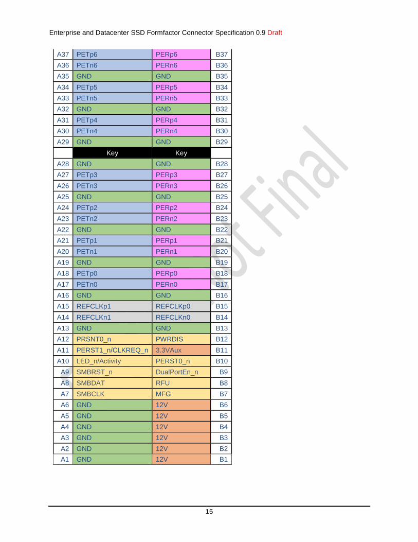
Enterprise and Datacenter SSD Formfactor Connector Specification 0.9 Draft
15
A37 PETp6 PERp6 B37
A36 PETn6 PERn6 B36
A35 GND GND B35
A34 PETp5 PERp5 B34
A33 PETn5 PERn5 B33
A32 GND GND B32
A31 PETp4 PERp4 B31
A30 PETn4 PERn4 B30
A29 GND GND B29
Key Key
A28 GND GND B28
A27 PETp3 PERp3 B27
A26 PETn3 PERn3 B26
A25 GND GND B25
A24 PETp2 PERp2 B24
A23 PETn2 PERn2 B23
A22 GND GND B22
A21 PETp1 PERp1 B21
A20 PETn1 PERn1 B20
A19 GND GND B19
A18 PETp0 PERp0 B18
A17 PETn0 PERn0 B17
A16 GND GND B16
A15 REFCLKp1 REFCLKp0 B15
A14 REFCLKn1 REFCLKn0 B14
A13 GND GND B13
A12 PRSNT0_n PWRDIS B12
A11 PERST1_n/CLKREQ_n 3.3VAux B11
A10 LED_n/Activity PERST0_n B10
A9 SMBRST_n DualPortEn_n B9
A8 SMBDAT RFU B8
A7 SMBCLK MFG B7
A6 GND 12V B6
A5 GND 12V B5
A4 GND 12V B4
A3 GND 12V B3
A2 GND 12V B2
A1 GND 12V B1

Enterprise and Datacenter SSD Formfactor Connector Specification 0.9 Draft
16
3 Card Edge and Connector Specification
For details of the card edge mechanicals, connector mechanicals, and connector performance requirements, please refer to the Protocol Agnostic Multi-Lane High Speed Connector specification (SFF-TA-1002).