Embed Size (px)
Citation preview

EQUALIZERS. HOW DO?BY: ANKIT JAIN

AGENDA
• DFE (Decision Feedback Equalizer) Basics
• FFE (Feed-Forward Equalizer) Basics
• CTLE (Continuous-Time Linear Equalizer) Basics
• More Complex Equalization

UNDERSTANDING THE DFE
• Continuous-Time Transfer Function of Channel (s-domain):
• Low Pass Filter
UNDERSTANDING THE DFE
• Discrete-Time Transfer Function of the Channel (z-domain):
H1(z) = 1 + a1z-1 + a2z-2 + a3z-3x[n] x[n] + a1x[n-1] + a2x[n-2] + a3x[n-3]

UNDERSTANDING THE DFE
• Pulse Response of Channel:• Top = Continuous Time Plot
• Bottom = Sampled Plot

PULSE RESPONSE (TESTBENCH)

NORMALIZED PULSE RESPONSE
• Next, normalize the pulse response:
• Set time of peak = n*T
• Post cursors = Response(T*(n+1)), Response(T*(n+2)), Response(T*(n+3)), …

POST CURSOR CALCULATIONS
• Calculated Postcursors:

UNDERSTANDING THE DFE
• Objective: Negate the effects of the post-cursors (a1, a2, a3…) through feedback FIR filter and accurate sampling (decision circuit)
• Pros:
• No amplification of noise+crosstalk
• Can make feedback filter adaptive
• Cons:
• Can only account for post-cursors (no pre-cursors)
• Critical feedback timing path

DFE TAP COEFFICIENTS
• If channel causes postcursorsa1, a2, a3, etc., …
• DFE tap coefficients must negate postcursors
• Thus, DFE tap coefficients = negative postcursors

ACTUAL IMPLEMENTATION OF DFE• Verilog code from HW shown to
right:
• READ THROUGH THIS CODE PROPERLY (it will help you significantly in the final project)

EFFECTS OF DFE (EYE DIAGRAM)
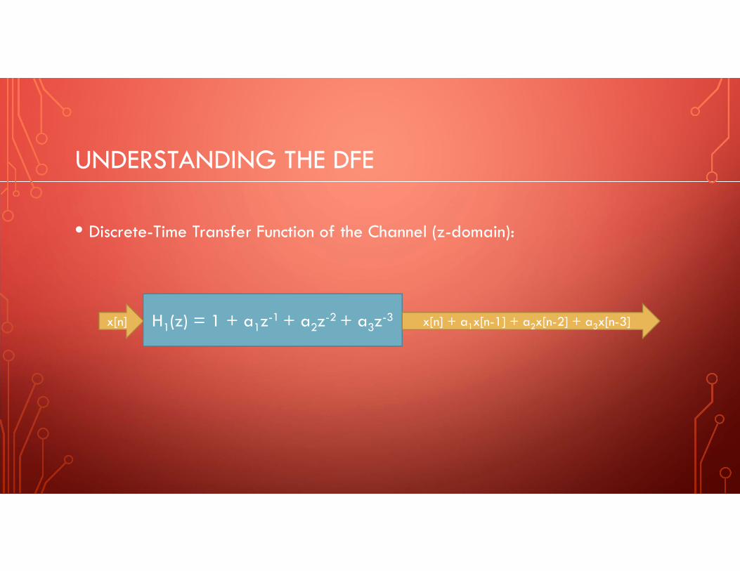
UNDERSTANDING FFE
• Pros• Simple to implement• Doesn’t amplify noise• Easily cancels precursors
• Cons• Signal Attuenated due to peak-power
limitation (output swing limit)• Hard to tune taps

FFE COEFFICIENT CALCULATION
• Need to calculate FFE coefficients such that convolution with channel results in solely the main cursor
• A = channel coefficients
• b = FFE coefficients
• c = equalized response

FFE COEFFICIENT CALCULATION (ONLY PRECURSOR)
• When solely eliminating precursor, matrix becomes:• Only b-1 and b0 matter to eliminate precursor
• Appending an extra zero at beginning in order to properly account for full sampled response
• A-matrix goes down to n amount of postcursors• Can match number with number of FFE coefficients
• However, more postcursors more ISI eliminated

EFFECTS OF FFEFull FFE Precursor Only

ACTUAL FFE DESIGN: NORMALIZE COEFFICIENTS
• Why?• Output swing is limited by headroom of
design
• Extra taps reduction of cursor’s tap weight
• In order to account for limitations, currents must add up to equal output termination current, meaning that:

CONTINUOUS TIME LINEAR EQUALIZATION
• Goal: To counteract the effects of the channel’s transfer function (s-domain)
• Accomplished via amplification• More amplification at operating frequency
• Less amplification at << operating frequency (DC Gain)
• Reduce higher frequency noise
DRAWBACKS OF CTLE DESIGN
• Drawbacks of RX CT Equalization:• Amplifying signal also amplifies noise + crosstalk (SNR stays same)
• Trade-off: High Gain + Output Swing vs. Small Size + Low Power Consumption
• When designing CTLE, need to iterate in order to optimize on all of these ends
• Still need to utilize filtering for noise and crosstalk
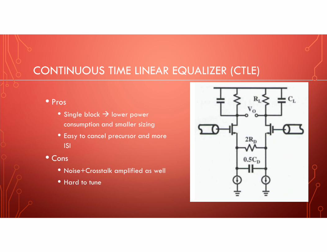
CONTINUOUS TIME LINEAR EQUALIZER (CTLE)
• Pros• Single block lower power
consumption and smaller sizing
• Easy to cancel precursor and more ISI
• Cons• Noise+Crosstalk amplified as well
• Hard to tune

CONTINUOUS TIME LINEAR EQUALIZER (CTLE)
• Active equalizer topology shown to right
• Differential amplifier with degeneration• Introduces an extra pole and zero
• Total: One zero, two poles
• Transfer Function = Peaking Amplifier

EQUATIONS FOR CTLE (DERIVED FROM CIRCUIT)

CTLE DESIGN PROCESS
1) Choose DC Gain and Peaking Gain (use insertion loss curve)
2) Decide optimal poles and zero frequency placements
3) Determine load capacitance from next stage (CDR input)
4) Determine equalizer output swing
5) Calculate component parameters to meet above specs
6) Test and optimize as necessary (iterative process)

CTLE TRANSFER FUNCTION (BODE PLOT)

EFFECTS OF CTLE (EYE DIAGRAM)
• Eyes• Yellow = TX end
• Green = Post-Channel
• Red = Post-EQ

MORE COMPLEX EQUALIZATION (SETUP)
• Full equalization setup with FFE + CTLE + DFE (in SERDES)

COMPLEX EQUALIZATION DESIGN PROCESS
1) Design CTLE to account for as much loss @ operating frequency
2) Design RX Driver Amp to account for remaining loss (~5-10 dB)
3) Analyze pulse response of channel+CTLE+RX Driver to calculate FFE coefficients (solely precursor) and test FFE behaviorally
4) Analyze pulse response again (no precursor this time) to determine postcursors for DFE coefficients and test DFE behaviorally