Embed Size (px)
Citation preview

Error Correction Code Protected Data Processing Units
N. Cucu Laurenciu*, T. Guptat, V. Savint, and S.D. Cotofana* * Computer Engineering Laboratory, Delft University of Technology, The Netherlands.
t CEA-LETI, MINATEC, Grenoble, France. {N .CucuLaurenciu, S.D.Cotofana }@tudelft.nl, {tushar.gupta, valentin.savin }@cea.fr
ABSTRACT
The significant uncertainty associated with current nanodevices fabrication and operation, calls for a circuit design paradigm change, which ought to actively embrace the inherently nanodevice unreliability to generate overall circuit architectures able to perform reliable computation. While for data storage units viable solutions exist, Data Processing Units (DPUs) are not amenable to a similar line of reasoning. The typical approach undertaken for fault-tolerant DPUs relies on modular redundancy (e.g., spatial, temporal), which while being effective from an error tolerance perspective, generally involves high area and/or performance impairments. This paper proposes a generic methodology to obtain reliable DPU implementations built with unreliable components by intimately intertwining Error Correcting Codes (ECCs) codecs with the DPU functionality. The ECC protected DPU architecture is derived cluster-wise with area and reliability constraints, by exploiting dependence relations (logical and w.r.t. shared area) between internal signals pertaining to the DPU and the ECC codec. To evaluate the error rate and performance implications, a multitude of test corners were considered (e.g., gate criticality, ECC type and structure, faulty and low complexity decoder, time-space redundancy) for an ECC protected 6-bit adder architecture. Simulation results reveal that the ECC embedding approach can be effective from both error rate and area perspective, for the Pareto designs with performance figures of merit situated in-between consecutive modular redundancy based design corresponding curves. The proposed approach is generic from the coding point of view, scalable, and enables a fine grained control of the DPU desired reliability degree and area overhead.
Keywords
reliable computing; unreliable devices; ECC; reliable nmctional units
1. INTRODUCTION
Permission to make digital or hard copies of all or part of this work for personal or classroom use is granted without fee provided that copies are not made or distributed for profit or commercial advantage and that copies bear this notice and the full citation on the first page. Copyrights for components of this work owned by others than ACM must be honored. Abstracting with credit is permitted. To copy otherwise, or republish, to post on servers or to redistribute to lists, requires prior specific permission and/or a fee. Request permissions from [email protected].
Nanoarch '16, July 18-20,2016, Beijing, China © 2016 ACM. ISBN 978-1-4503-4330-5/ 16/ 07 ... $15.00
DOl: http://dx.doi.org/1O.1l45/2950067.2950093
37
As CMOS technology down scaling is approaching fundamental limitations (e.g., photolitographic manufacturing, physical as transistor feature reaches the size of a few atoms and economical with diminishing returns) the nanodevice� physical and electrical parameters variability is greatly increased [1]. As a result, devices no longer function deterministically but, their de facto operation is rather governed by a stochastic process, which in turn significantly impacts their reliability. Furthermore, even when operating correctly, the nanodevices exhibit an increased susceptibility to transient and permanent errors. On the other hand, nascent technologies, e.g., single electron tunneling, carbon nanotubes, molecular devices, while holding promise as alternatives to silicon semiconductors, are still in their infancy and deficitary in mass production means [2]. Therefore, a seemingly natural avenue for the CMOS technology scaling is to perform reliable nanoscale computing with unreliable devices, which reiterates once again the early vacuum tubes challenge.
To this effect, in the case of nanoscale memories, ErrorCorrecting Codes (ECCs) are traditionally used, proving to be a viable solution [3], [4]. The data are encoded with an ECC prior to their storage and afterwards transient bit flipping faults can be periodically detected and corrected. For digital logic however a similar line of reasoning is not applicable any longer, as in this case it is not the ECC protected memory content that is directly affected by errors, but the hardware (the logic gates) whose correlated and cumulated errors effect is reflected in the DPU ECC protected outputs. Thus while for memories ECC redundancy is generated only as a function of the data to be protected, prior to its storage, for DPUs ECC redundancy has to be generated during the computation of the to be protected data. The conventional solution for logic is to employ some form of von Neumann style modular redundancy, which can be implemented in either time (e.g., repeat the same computation on the same hardware) , or space (e.g., execute the same computation in parallel on hardware replicas) [5]. From an information theory point of view, modular redundancy (in both space and time) rely on repetition coding. For modular redundancy the output is expected to be the same even if it undergoes different computation conditions (i.e., (i) for temporal redundancy different environmental conditions, and (ii) for spatial redundancy different hardware replicas, which may be implemented in different technologies, logic styles etc.) . This is similar to transmitting the same data over different channels. While benefiting from implementation simplicity,
the modular redundancy approach is rather inefficient from the coding point of view. Thus arises the natural question of whether an ECC with a better error correction capability, which requires only a small constant overhead in order to protect a circuit logic against random bit-flip faults can be employed.
The main research question that we address in this paper can be formulated as follows: Given a fabrication technology able to provide basic circuit components, i.e., logic gates, with an error rate of lO-x in certain environmental conditions, can we systematically derive a circuit topology able to implement a given Boolean function F such that the circuit output Word Error Rate (WER) is lO-y with y > x
(noting that y can be significantly smaller than x if no fault tolerance technique is used), while abiding to a set of design constraints in terms of area, delay, and power consumption? To this end, we propose to augment the traditional Boolean algebra design avenue with information theory concepts, i.e., to make use of ECCs in order to improve the reliability of circuits built out of unreliable devices. The key element behind this approach is the realization of an intimate intertwining between the original circuit whose Primary Outputs (POs) should be ECC protected, and the afferent codec hardware. Specifically, the ECC protected circuit (whose outputs may or may not include the original circuit POs, depending on the ECC type) is synthesized in independent clusters based on certain criteria (i.e., logical dependencies and shared area amount) while targeting a Word Error Rate (WER) after decoding smaller than the fabrication technology determined gate error rate.
The detailed methodology for deriving the ECC protected circuit architecture is presented in Section 2. We employ as discussion vehicle a 6-bit Brent-Kung parallel prefix adder and investigate the influence of several codes and design strategies upon the protected adder WER/area merits. As described in Section 3, we evaluate a multitude of test corners by: (i) varying ECC parameters (error correction capacity) and structure (ECC type, modularized ECC), (ii) varying gate criticality (w.r.t. circuit POs inflicted damage) to identify an optimum WER/area design point, and (iii) considering different architectural optimizations for both encoder and decoder (gate criticality aware synthesis for the encoder, low complexity architecture for the decoder). Simulation results reveal that the proposed approach can be effective from both WER and area perspective for the Pareto designs with performance figures of merit situated in-between consecutive modular redundancy based design counterparts. Section 4 concludes the paper with a summary of the main points and results.
2. GENERAL FRAMEWORK AND SIMU
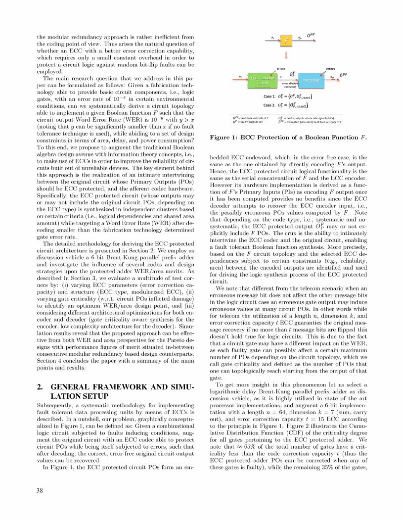
LATION SETUP Subsequently, a systematic methodology for implementing fault tolerant data processing units by means of ECCs is described. In a nutshell, our problem, graphically conceptualized in Figure 1, can be defined as: Given a combinational logic circuit subjected to faults inducing conditions, augment the original circuit with an ECC codec able to protect circuit POs while being itself subjected to errors, such that after decoding, the correct, error-free original circuit output values can be recovered.
In Figure 1, the ECC protected circuit POs form an em-
38
Figure 1: ECC Protection of a Boolean Function F.
bedded ECC codeword, which, in the error free case, is the same as the one obtained by directly encoding F's output. Hence, the ECC protected circuit logical functionality is the same as the serial concatenation of F and the ECC encoder. However its hardware implementation is derived as a function of F's Primary Inputs (PIs) as encoding F output once it has been computed provides no benefits since the ECC decoder attempts to recover the ECC encoder input, i.e., the possibly erroneous POs values computed by F. Note that depending on the code type, i.e., systematic and nosystematic, the ECC protected output O� may or not explicitly include F POs. The crux is the ability to intimately intertwine the ECC codec and the original circuit, enabling a fault tolerant Boolean function synthesis. More precisely, based on the F circuit topology and the selected ECC dependencies subject to certain constraints (e.g., reliability, area) between the encoded outputs are identified and used for driving the logic synthesis process of the ECC protected circuit.
We note that different from the telecom scenario when an erroneous message bit does not affect the other message bits in the logic circuit case an erroneous gate output may induce erroneous values at many circuit POs. In other words while for telecom the utilization of a length n, dimension k, and error correction capacity t ECC guaranties the original message recovery if no more than t message bits are flipped this doesn't hold true for logic circuits. This is due to the fact that a circuit gate may have a different impact on the WER, as each faulty gate can possibly affect a certain maximum number of POs depending on the circuit topology, which we call gate criticality and defined as the number of POs that one can topologically reach starting from the output of that gate.
To get more insight in this phenomenon let us select a logarithmic delay Brent-Kung parallel prefix adder as discussion vehicle, as it is highly utilized in state of the art processor implementations, and augment a 6-bit implementation with a length n = 64, dimension k = 7 (sum, carry out), and error correction capacity t = 15 ECC according to the principle in Figure 1. Figure 2 illustrates the Cumulative Distribution Function (CDF) of the criticality degree for all gates pertaining to the ECC protected adder. We note that :::::; 65% of the total number of gates have a criticality less than the code correction capacity t (thus the ECC protected adder POs can be corrected when any of these gates is faulty), while the remaining 35% of the gates,
FF
ECC Protected CC ProtecteCircuit
E DECODER
errors errors
Case 1. = ,,, ___
Case 2. = ___
= fault-free outputs of F= faulty outputs of F
= faulty outputs of encoder (parity bits)= estimated (decoded) fault-free outputs of F
error affected error affecteddcodeword

0.9 0.8 0.7 0.6
LL
80.5 r the number of erroneous outputs exceeds the code correction capacity t
0.4 0.3 0.2 34 gates topologically
22 gates, 80% of the time 0.1
oU---���----�--�--�----�--� o 10 t 20 30 40 so 60 70
Criticality Degree
Figure 2: Gate Criticality Statistics.
topologically speaking, can induce more than t errors to the ECC protected circuit outputs (and thus diminish the ECC efficiency). Furthermore, multiple gates may be faulty concomitantly, even if individually each faulty gate has a criticality < t. Hence for an effective ECC protection it is highly desirable that the augmented circuit is built with gates that exhibit a criticality as small as possible w.r.t. the threshold t. On the other hand, one may note that the gate criticality is merely a topological upper bound, as in practice, due to fault masking and preponderant workload patterns, the maximum number of outputs that can actually be affected by a faulty gate is less. Indeed, when subjecting the ECC protected adder to a random 10000 13-bit workload, from a total of 34 gates with a topological (maximal) criticality > t, only 22 gates actually affect 80% of the time more than t outputs. While this suggests that a reduced number of gates (22) should be targeted by the circuit redesign in view of criticality reduction below threshold t (e.g., via gate replication), it still remains a prohibitively complex process to impose constraints on individual gates, while maintaining the error resiliency characteristic of the remaining circuit structure, and at the same time keeping the overall area footprint within reasonable limits.
In view of this, a more judicious architectural solution would be to consider a higher level of granularity, i.e., an output clustering approach. Specifically, to derive the ECC protected circuit architecture, we propose the following methodology:
• Step 1. The ECC protected circuit outputs O� are first aggregated in groups of x, the desired maximum gate criticality, based on affinity w.r.t. the area shared between them.
• Step 2. RTL synthesis is then performed with area / timing / power constraints for each group of outputs. Thus each O� group is synthesized as a function of all the original circuit PIs, and has its own cone of logic, independent of the other group cones. In this way, within each logic cone, the reliability constraints (i.e., gate criticality::; the number of group outputs), are always satisfied.
For evaluation purpose, we select based on decoding complexity and code performance rationale the following block linear codes [6]: (i) Reed-MUller codes, and (ii) linear codes optimal w.r.t. the code length, for given error correction
Generate Input Bits
Compare primary output
bits
Figure 3: Reliability Evaluation Framework.
capacity and information size. To maintain the simulation time within reasonable limits and allows for the evaluation of a large number of codes and design strategies we limit the investigation to a 6-bit Brent-Kung parallel prefix adder but we note that the proposed approach is general and can be applied to any Boolean circuit. To assess the merit of the ECC enhanced designs we consider the following two metrics: (i) total number of 2-input gates, as preliminary area indicator, and (ii) WER as reliability monitor. The logic synthesis is performed using Cadence RTL Compiler [7] for a commercial 40nm LP CMOS technology node and for a fair comparison, only 2-input basic gates are employed. The reliability evaluation flow follows the block scheme depicted in Figure 3. A statistically relevant batch of 10 million circuit input vectors are generated via a maximum period 31-bit shift register pseudo-random number generator. The original circuit without any codec, assumed error-free in this case (no errors injected), is then simulated and the obtained PO values are saved to provide the reference for subsequently deriving the WER statistics. For the ECC codec enhanced circuit reliability simulation, we consider homogeneous (identical) gate failure probability. We concern ourselves with transient and permanent faults manifested for logic gates as single bit-flips of their outputs. For bit-flip inflicting on a gate output with a given probability of failure, the xorshift128+ generator [8] is employed. Once the original, error-free circuit and the ECC codec enhanced error-prone one are both simulated, their POs are compared to each other in order to derive the WER statistics of interest.
3. DESIGN SPACE EXPLORATION Having presented the methodology to derive the ECC protected circuit architecture, we are now in position to investigate the implications of various architectural and ECC related strategies, from WER and area standpoints. Subsequently, we adhere to the notation MR-z for a modular redundancy scheme and ECC[n, k, t]_Cx-yy, where (i) ECC can be RM for Reed-Mi.iller codes, or Opt for optimal codes; (ii) [n, k, t] denote the ECC parameters - code length (encoded bits) n, info size (bits to be protected) k, and error correction capacity t; (iii) Cx denotes the maximum gate criticality; and (iv) vy is used for architecture versioning.
3.1 Gate Criticality To explore the gate criticality influence on WER, we consider an optimal systematic code Opt[58, 7, 13] and vary the ECC protected adder gate criticality from 2 to 14. Figure 4 illustrates the WER and area overhead of the ECC protected adder relative to the baseline design and the MR protected counterparts. The figure reveals that the area overhead is increasing as the gate criticality decreases. This is obvious since the outputs are divided in more groups and as a result the amount of area shared gets smaller. Conversely
39

Figure 4: WER/ Area vs. Gate Criticality.
Figure 5: WER/ Area for Code Correction Capacity t=l1.
the WER curves improve with the gate criticality decrease. The reason is twofold: (i) there is a smaller probability that faulty gates will corrupt multiple outputs (as there is less area shared between the group outputs), and (ii) there is a higher probability of fault masking occurrence (up to a certain design inflexion point after which the bigger area facilitates less and less fault masking). Summarizing, when varying the gate criticality, efficient design points can be identified between the MR curves, with effective WER/area trade-offs. For instance the design Opt [58, 7, 13]_C9_vl has an area penalty of 4.3x baseline (which is 14% less than the MR-5 area and 43% more than the MR-3 area) and a WER curve that lies approximately in the middle between the MR-3 and the MR-5 WER curves.
3.2 Code Correction Capacity For this test corner, 8 codes optimal w.r.t. the codeword length n for fixed information size k (i.e., 7) and an error correction capacity t spanning from 5 to 17 were investigated ([n, k, t] E { [26, 7, 5]' [31, 7, 6], [34, 7, 7]' [42, 7, 9]' [49, 7, 11]' [58, 7, 13]' [63, 7, 15], [74, 7, 17] }). Figure 5 illustrates the WER and area figures obtained for the Opt[49, 7, 11] code. One can observe: (i) the design Opt[49; 7; l1]_GLvl exhibits a WER that is very close to the MR-5 one, while area wise it requires 10% less area, (ii) the design Opt[49; 7; 11]_G8_vl has a WER curve that is situated approximately in the middle between the MR-3 and
40
MR-5 curves, with an area overhead of 33% relative to the MR-3 area, but with 20% less area when compared to the MR-5 area, and (iii) the design Opt[49; 7; 11]_G9_vl shows a WER curve that is slightly better than the MR-3 one, while requiring 33% more area, trade-off which is not justified as in the (i) and (ii) cases. In the figure we plotted for the Opt[49; 7; 11] code, the merits of only a few designs which correspond to a gate criticality of 5 to 9 and certain c1usterization optimization points. However, several design architectures were obtained with WER in-between two consecutive MR WER curves (e.g., between the MR-3 and MR-5 WER curves). Thus, from the previous results it can be concluded that the coding approach offers a much higher flexibility and achievable WER range granularity when compared to the MR approach. Even though for the design points with WER curves approaching the MR ones, the area penalty is higher which renders the coding approach rather inefficient, in-between the MR curves, the EGG approach enables WER curves and area figures which are bounded by two consecutive modular redundancy figures. For instance between the MR-3 and MR-5 WER curves, several intermediary curves can be obtained via EGG, at the expense of an area whose value is lower bounded by the MR-3 area and upper bounded by the MR-5 area. This indicate that, as a function of the gate criticality degree and the check bits clustering policy efficiency, such an EGG embedding design with good performance (WER as well as area) relative to two consecutive modular redundancy designs, can always be found.
3.3 ECC Type Both systematic and non-systematic block linear codes were considered. The systematic code has the advantage that the original circuit POs are part of the codeword. This implies that the check bits c1usterization can either exclude those bits identical with the original circuit POs (in which case the original circuit architecture is preserved as it is in a single cluster - encoding non-intrusiveness which is most often desirable) or include all codeword check bits. For the nonsystematic code, only the latter situation is applicable as the original circuit POs are not part of the codeword but, are obtained indirectly via decoding. For evaluation we considered Reed-MUller codes as the same decoder architecture can be employed for both the systematic and non-systematic forms. It was observed that the systematic RM code behaves better than the non-systematic counterpart from both the WER and area standpoints. Next we considered optimal length codes for fixed error capacity and information size [9] [10]. When compared to RM codes with similar codeword length, the RM codes enabled better WER and area figures. However, when the code correction capacity and its length are varied, the optimal codes provide a slightly better alternative to shortening and puncturing of the Reed-Muller codes. From the point of view of the decoder architectural complexity, the Reed-Muller EGGs have a significant advantage over the optimal codes, as they can be decoded efficiently using majority logic. Summarizing, as simulation results (omitted herein due to space limitations) indicate, systematic ReedMUller codes seem to present the greatest potential among the linear block codes, with respect to the codec architectural complexity, as well as with induced WER figures.
3.4 Time-Space Redundancy As a functional unit (e.g., an adder) workload is usually not
1.00E-07
1.00E-06
1.00E-05
1.00E-04
1.00E-03
1.00E-02
1.00E-01
1.00E+00
MR_3 MR_5 MR_7
MR_11 Opt[58,7,13]_C5_v1 Opt[58,7,13]_C6_v1
Opt[58,7,13]_C9_v1 Opt[58,7,13]_C10_v1 Opt[58,7,13]_C12_v1
adderOrig
MR_9
Opt[58,7,13]_C7_v1
Opt[58,7,13]_C14_v1 Opt[58,7,13]_C4_v1 Opt[58,7,13]_C3_v1 Opt[58,7,13]_C2_v1
Design#
gates×
increase
AdderOrig (baseline)
Opt[58,7,13]_C2_v1 835 12.8
Opt[58,7,13]_C3_v1 613 9.4
Opt[58,7,13]_C4_v1 500 7.8
Opt[58,7,13]_C5_v1 415 6.4
Opt[58,7,13]_C6_v1 361 5.6
Opt[58,7,13]_C7_v1 329 5.1
Opt[58,7,13]_C9_v1 283 4.3
Opt[58,7,13]_C10_v1 247 3.8
Opt[58,7,13]_C12_v1 220 3.4
Opt[58,7,13]_C14_v1 209 3.2
MR_3 195 3.0
MR_5 325 5.0
MR_7 455 7.0
MR_9 585 9.0
MR_11 715 11.0
1.00E-07
1.00E-06
1.00E-05
1.00E-04
1.00E-03
1.00E-02
1.00E-01
1.00E+00
MR_3 MR_5 MR_7
Opt[49,7,11]_C6_v1 Opt[49,7,11]_C7_v2 Opt[49,7,11]_C7_v1
adderOrig
Opt[49,7,11]_C5_v1
Opt[49,7,11]_C8_v1 Opt[49,7,11]_C9_v1
Design#
gates×
increase
AdderOrig (baseline)
Opt[49,7,11]_C5_v1 387 6.0
Opt[49,7,11]_C6_v1 359 5.5
Opt[49,7,11]_C7_v2 330 5.1
Opt[49,7,11]_C7_v1 291 4.5
Opt[49,7,11]_C8_v1 262 4.0
Opt[49,7,11]_C9_v1 259 4.0
MR_3 195 3.0
MR_5 325 5.0
MR_7 455 7.0

�adderOrig
....,a.-MR 3
�RM[64,7,15LCB_vl_BC
....... RM[64,7,15LCB_vl_LCdec_BC
�adderOrig
_MR_3_WC
-RM[64,7,lSLCB_vl_WC
-roRM[64,7,15LCB_vl_LCdec_WC
PDEC = PCIRC
�adderOrjg
_MR_3_1E-3rel
_RM[64,7,lSLCB_vl_1E-3rel
�adderOrig
....... MR_3_1E-2rel
-roRM[64,7,15LCB_vl_lE-2rel
PDEC = 10-2 • PCIRC I
CIRC - ECC Protected Circuit
Figure 6: WER for Non-Ideal Decoding.
SET,
5IT, 5IT,
t,-f""L
c:::::::::�> Time Redundancy
forF
Figure 7: Time- Space Redundancy.
sporadic in time, but rather consists in batches of multiple consecutive operations, we investigated whether a spatial redundancy approach could be taken advantage of, en route to WER improvement. Specifically, a single code could be employed to protect not only the result of one addition, but the results of p consecutive additions altogether. We continue the discussion subsequently assuming a systematic code, however a similar rationale holds true for nonsystematic codes. A straight forward approach is a spatialonly approach, i.e., to make use of p adder replicas, as illustrated in Figure 7, each with its own different set of inputs. The codeword consists of (i) p x no bits provided by each adder replica F and (ii) the remaining m parity bits which are derived by the subcircuit P as a function of all p adders primary inputs. This perspective incurs however a high area penalty, which is not justified by its corresponding WER improvement. To alleviate the area overhead, a compound spatio-temporal redundancy is sought. Concretely, this translates to: (i) instead of replicating p times the adder, a single instance is used and subjected to p consecutive workloads to generate the first p x no codeword bits, and (ii) the remaining m codeword bits are computed as in the previous spatial-only redundancy approach, as a function of all the p adders PI values. For practical evaluation, we first explored a time redundancy factor of 4, which translates to 28 bits to be protected via ECC (RM[128, 28, 15]). We obtained a WER curve which lies between the MR-3 and MR-5 WER curves, while area-wise is 31.8x baseline, as compared to 3 x and 5 x baseline for the MR-3 and MR-5 designs, respectively. The high area is a direct consequence of the high codeword size (128), as the encoded bits are a function of all 8 6-bit adder operands and 4 carry-in bits. A rela-
tively high criticality degree (7) was employed to diminish the area overhead but its further increase would result in a WER worse than the MR-3 one. In an effort to reduce the number of ECC bits, and thus the total area footprint, we considered next a time redundancy factor of 2, which translates to 14 bits that necessitate ECC protection, resulting in a 55-bit codeword ((RM[55, 14, 7]) code). As expected, the area decreased substantially by more than 3x w.r.t. the previous analyzed cases, to yield 9.7x baseline. While the WER curve is slightly better than the MR-3, this comes at a still high area penalty increase (i.e., � 3 x MR-3).
3.5 Non-Ideal Decoding Thus far we assumed an ideal error-free decoding but in practice the decoder is also subject to the environmental aggresion even though it can be designed with tighter margins and reliability constraints, such that in-field it exhibits a much lower error rate than the ECC protected circuit. In view of this, we considered different non-systematic ReedMUller codes, and evaluated the after decoding WER. We split the design into two gate failure probability islands, which realistically can be realized by over-design or by making use of two fabrication technology nodes, i.e., an advanced one for the ECC protected adder and an older more reliable one for the decoder. For simulations, a one-step parameterizable Reed-Muller majority logic decoder was employed. To grasp the WER bias an ideal decoder can induce we plotted in Figure 6 the WER curves for ideal vs. faulty Reed-MUller decoder, for different decoders gate probability of failure: (i) WC - worst case, i.e., the decoder gates probability of failure is equal to the ECC protected circuit gates probability of failure, (ii) BC - best case, i.e., the decoder is error-free, (iii) 1E-3rel - the decoder gates probability of failure is 103 x less than the ECC protected circuit counterpart, and (iv) 1E-2rel - the decoder gates probability of failure is 102 x less than the ECC protected circuit counterpart. As depicted in Figure 6 the MR-3 and RM designs exhibit similar WER curves (slightly better for the MR-3). When compared to the original adder WER, Figure 6 reveals slightly better WER curves for the MR-3 and RM designs, when both the ECC protected circuit and decoder operate under the same gate failure probability. The 1E-3rel case gives almost identical WER as the BC case, while the WER curves for the 1E-2rel case lie approximately in the middle of the BC and WC case. As intuited, the decoder probability of failure has a big impact on the system WER, and hence shouldn't be disregarded. From
41
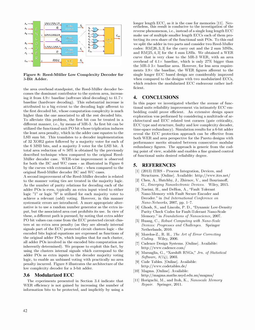
Figure 8: Reed-Muller Low Complexity Decoder for 3-Bit Adder.
the area overhead standpoint, the Reed-Muller decoder becomes the dominant contributor to the system area, increasing it from 4.9x baseline (software ideal decoding) to 41.7x baseline (hardware decoding). This substantial increase is attributed to a big extent to the decoding logic afferent to the first decoded bit, whose computation complexity is much higher than the one associated to all the rest decoded bits. To alleviate this problem, the first bit can be treated in a different manner, i.e., by means of MR-3. As first bit can be utilized the functional unit PO bit whose triplication induces the least area penalty, which in the adder case equates to the LSB sum bit. This translates to a decoder implementation of 32 XOR2 gates followed by a majority voter for each of the 6 MSB bits, and a majority 3 voter for the LSB bit. A total area reduction of :::::; 50% is obtained by the previously described technique when compared to the original ReedMuller decoder case. WER-wise improvement is observed for both the BC and WC cases - as illustrated in Figure 6 by the curves with extension LCdec - when compared to the original Reed-Muller decoder BC and WC cases. A second improvement of the Reed-Muller decoder is related to the manner voting ties are treated in the majority logic. As the number of parity relations for decoding each of the adder POs is even, typically an extra input wired to either logic "1" or logic "0" is utilized for each majority voter to achieve a relevant (odd) voting. However, in this manner systematic errors are introduced. A more appropriate alternative is to use a random number generator as the extra input, but the associated area cost prohibits its use. In view of these, a different path is pursued, by noting that extra adder PO bit values can come from the ECC protected circuit clusters at no extra area penalty (as they are already internal signals part of the ECC protected circuit clusters logic - the encoded bits logical equations are expressed as functions of the original adder POs, which implies that for each cluster, all adder POs involved in the encoded bits computation are inherently determined). We propose to exploit this fact, by using the clusters internal signals which correspond to the adder POs as extra inputs to the decoder majority voting logic, to enable an unbiased voting with practically no area penalty incurred. Figure 8 illustrates the architecture of the low complexity decoder for a 3-bit adder.
3.6 Modularized ECC The experiments presented in Section 3.4 indicate that
WER efficiency is not gained by increasing the number of information bits to be protected, and implicitly by using a
42
longer length ECC as it is the case for memories [11]. Nevertneless, this result is conducive to the investigatIOn of the reverse phenomenon, i.e., instead of a single long length ECC make use of multiple smaller length ECCs each of them protecting its own share of the functional unit POs. To this end we split the adder in two parts and consider two Reed-Muller codes: RM[26, 3, 3] for the carry out and the 2 sum MSBs, and RM[25, 4, 3] for the 4 sum LSBs. We obtained a WER curve that is very close to the MR-3 WER, with an area overhead of 4.1 x baseline, which is only 27% bigger than the MR-3 3x baseline area. However, for less area requirements 3.9x the baseline, the WER figures afferent to the single longer ECC based design are considerably improved when compared to the designs with two modularized ECCs, which renders the modularized ECC endeavour rather inefficient.
4. CONCLUSIONS In this paper we investigated whether the avenue of functional units reliability improvement via intimately ECC embedding could prove efficient. An extensive design space exploration was performed by considering a multitude of architectural and ECC related test corners (gate criticality, ECC type and structure, faulty and low complexity decoder, time-space redundancy). Simulation results for a 6-bit adder reveal the ECC protection approach can be effective from both WER and area perspective for the Pareto designs with performance merits situated between consecutive modular redundancy figures. The approach is generic from the coding point of view, scalable and enables a fine grained control of functional units desired reliability degree.
5. REFERENCES [1] (2013) ITRS - Process Integration, Devices, and
Structures. [Online]. Available: http://www.itrs.net/ [2] Chen, A., Hutchby, J., Zhirnov, V., and Bourianoff,
G., Emerging Nanoelectronic Devices. Wiley, 2015. [3] Naeimi, H., and DeHon, A., "Fault Tolerant
Nano-Memory with Fault Secure Encoder and Decoder." in 2nd International Conference on
Nano-Networks, 2007, pp. 1-7. [4] Ghosh, S., and Lincoln, P. D., "Dynamic Low-Density
Parity Check Codes for Fault-Tolerant Nano-Scale Memory." in Foundations of Nanoscience, 2007.
[5] Huang, C., Robust Computing with Nano-Scale
Devices: Progresses and Challenges. Springer Netherlands, 2010.
[6] Morelos-Z., R. H., The Art of Error Correcting
Coding. Wiley, 2006. [7] Cadence Design Systems. [Online]. Available:
http://www.cadence.com/ [8] Marsaglia, G., "Xorshift RNGs," 1m. of Statistical
Software, 8(14), 2003. [9] Code Tables. [Online]. Available:
http://www.codetables.de/ [10] Magma. [Online]. Available:
http://magma.maths.usyd.edu.au / magma/ [11] Horiguchi, M., and Itoh, K., Nanoscale Memory
Repair. Springer, 2011.