Embed Size (px)
Citation preview

ESP-12F WiFi module
Specifications
Version 1.0
August 23, 2015
Disclaimer and Copyright Notice
Information in this document, including URL address for reference, subject to change without notice.
Document "AS IS", WITHOUT ANY WARRANTY, including merchantability, fitness for any particular
purpose or non-infringement guarantee in any guarantees and any proposal, specification or sample
mentioned in his place. This document assumes no liability, including liability for infringement of any
patent behavior of the use of this information within the document produced. The documents in this
not confer any intellectual property rights to prohibit estoppel or otherwise Use license, either
express or implied license.
Wi-Fi Alliance members logos are owned by all the Wi-Fi Alliance.
All trade names mentioned in the text, trademarks and registered trademarks are the property of
their respective owners, and are hereby acknowledged.

CAUTION
Since the product version upgrade or other reasons, the contents of this manual are subject to
change. Shenzhen Shun Technology Co., Ltd. can be claimed without any notice or prompt
information in this manual is subject to change reservations. This manual only as a guide, Shenzhen
Shun Technology Co., Ltd. can make every effort to provide accurate information in this manual, but
Shenzhen Shun Technology Co., Ltd. can not ensure the manual is no error, all statements in this
manual, information and suggestions do not constitute any kind, express or implied.
Table of Contents
1. Product Overview …………………………………………………………………….....2
1.1 Features …………………………………………………………………………3
1.2. The main parameters ……………………………………………..…....4
2. Interface Definition ……………………………………………………………..……….5
3. The shape and size………………………………………………………………………..7
4. Functional Description …………………………………………………………….……9
4.1. MCU ……………………………………………………………………………..9
4.2 Storage Description ……………………………………………………….9
4.3. Crystal ………………………………………………………………………….9
4.4 Interface Description ……………………………………………………10
4.5. Maximum Ratings ……………………………………………………….11
4.6. The recommendations of the working environment ….11
4.7 Digital Port Characteristics ……………………………………….….11
5. RF parameters …………………………………………………………………….………12
6. Power ………………………………………………………………………………….……..13
7. tilt warming………………………………………………………………………….……..14
8. Schematic ……………………………………………………………………………………15

9. Product Trial…………………………………………………………………………………16
1. Product Overview
ESP-12F WiFi module is a security technology developed by the Letter to the module integrated core
processor ESP8266 smaller package size Tensilica L106 industry-leading ultra-low power 32-bit micro
MCU, with 16 compact mode frequency support 80 MHz and 160 MHz, supports RTOS, integrated
Wi-Fi MAC / BB / RF / PA / LNA, on-board antenna.
The module supports standard IEEE802.11 b / g / n protocol, a complete TCP / IP protocol stack. Users
can use the module for the existing equipment to add networking capabilities, you can build a
separate network controller.
ESP8266 is a high performance wireless SOC, at the lowest cost to provide maximum practicality, the
WiFi functionality into other systems offer endless possibilities.
Figure 1 ESP8266EX Chart
ESP8266EX is a complete and self-contained WiFi network solution that can run independently, it can
also be mounted as a slave to another host MCU operation. ESP8266EX when the device is mounted
as the only application should 一 Use processor can boot directly from the external flash memory.
Built-in cache system is conducive to mention high- performance and reduce memory requirements.
Also 一 species case, ESP8266EX responsible for wireless Internet access WiFi adapter undertake the
task, you can add it to any microcontroller-based design, the connection is simple and easy YES,
simply by SPI / SDIO interface or I2C / UART port can.

ESP8266EX powerful processing chip and the memory can be subjected to, it can be integrated
through the GPIO port sensors and other application-specific equipment to achieve the lowest
pre-development and operation occupy minimal system resources.
Within a highly integrated chip ESP8266EX, including the antenna switch balun, power management
converter, thus with minimal external circuitry, and the entire solution including front-end modules,
including in the design of the PCB occupied space to a minimum.
There ESP8266EX system manifested leading features are: energy in the sleep / wake quickly switch
between modes, with low-power operation of the adaptive radio bias, front-end signal processing
functions, troubleshooting and radio systems coexist characteristic for the elimination of cellular /
Bluetooth / DDR / LVDS / LCD interference.
1.1 Features
• 802.11 b / g / n
• Built Tensilica L106 ultra-low power 32-bit micro MCU, clocked at 80 MHz and supports 160 MHz,
support for RTOS
• Built-in 10 bit precision ADC
• Built-in TCP / IP protocol stack
• Built TR switch, balun, LNA, power amplifier and matching network
• Built-in PLL, voltage regulator and power management components, 802.11b mode +20 dBm output
power
The guard interval • A-MPDU, A-MSDU aggregation and 0.4 s of
• WiFi @ 2.4 GHz, supports WPA / WPA2 security mode
• Supports remote upgrade and cloud AT OTA upgrade
• Support STA / AP / STA + AP mode
• Support Smart Config function (including Android and iOS devices)
• HSPI, UART, I2C, I2S, IR Remote Control, PWM, GPIO
• Deep sleep holding current 10 uA, shutdown current of less than 5 uA
• Within 2 ms of wake-up, connect and transfer data packets
• Standby power consumption is less than 1.0 mW (DTIM3)
• Operating temperature range: -40 - 125

1.2. The main parameters
Table 1 describes the main parameters of the module.
Table 1 Parameters Table
Category Parameters Explanation
Radio parameters
Standards Certification FCC/CE/TELEC
Wireless Standard 802.11 b/g/n
Frequency Range 2.4GHz2.5GHz (2400M2483.5M)
Hardware parameters
Data access UART/HSPI/I2C/I2S/Ir Remote Contorl
GPIO/PWM
Operating Voltage 3.0~3.6V(Suggested 3.3V)
Working current Mean: 80mA
Operating temperature 40°~125°
Storage temperature At room temperature
Package Size 16mm*24mm *3mm
External Connector N/A
Software parameters
Wireless Network Mode station/softAP/SoftAP+station
Security Mechanism WPA/WPA2
Encryption Type WEP/TKIP/AES
Upgrading firmware Local serial programming / Cloud Upgrade / Host Download Burn
Software Development Supports customerdefined server
To provide secondary development SDK
Network protocol IPv4, TCP/UDP/HTTP/FTP
User Profiles AT + instruction set, cloud server, Android/iOS APP
2. Interface Definition
ESP-12F received a total of 18 interfaces, Table 2 is the interface definition.

Figure 2 ESP-12F pin map
Table 2 ESP-12F pin function definitions
No. Pin Name Function Description
1 RST Reset Module
2 ADC A / D conversion result. Input voltage range of 0 ~ 1V, in the range: 0 to 1024
3 EN Chip Enable end, high effective
4 IO16 GPIO16; do wake deep sleep when receiving RST pin。
5 IO14 GPIO14; HSPI_CLK
6 IO12 GPIO12; HSPI_MISO

7 IO13 GPIO13; HSPI_MOSI; UART0_CTS
8 VCC powered by 3.3V
9 CS0 Chip Select
10 MISO Slave Master Input Output
11 IO9 GPIO9
12 IO10 GBIO10
13 MOSI Master Out Slave
14 SCLK Clock
15 GND GND
16 IO15 GPIO15; MTDO; HSPICS; UART0_RTS
17 IO2 GPIO2; UART1_TXD
18 IO0 GPIO0
19 IO4 GPIO4
20 IO5 GPIO5
21 RXD UART0_RXD; GPIO3
22 TXD UART0_TXD; GPIO1
Mode GPIO15 GPIO0 GPIO2
UART Download mode Low Low High
Flash Boot Mode Low High High
Parameters Smallest value
Typical values
Maximum Unit
Input Frequency 2412 2484 MHz
Input resistance 50 Ω
Input reflection 10 dB
72.2 Mbps down, PA output power 14 15 16 dBm
Under 11b mode, PA output power 17.5 18.5 19.5 dBm

Sensitivity
DSSS, 1 Mbps 98 dBm
CCK, 11 Mbps 91 dBm
6 Mbps (1/2 BPSK) 93 dBm
54 Mbps (3/4 64QAM) 75 dBm
HT20, MCS7 (65 Mbps, 72.2 Mbps) 72 dBm
Adjacent suppression
OFDM, 6 Mbps 37 dB
OFDM, 54 Mbps 21 dB
HT20, MCS0 37 dB
HT20, MCS7 20 dB
3. The shape and dimensions
ESP-12F SMD module appearance Size inch of 16mm * 24mm * 3mm (Figure 3). The module uses a
capacity of 4MB, packaged as SOP-210 mil of SPI Flash. Modules using a 3 DBi of PCB-board antenna.

Figure 3 ESP-12F module appearances

Figure 4 ESP-12F module size view of a smooth surface
Table 5 ESP-12F Module Size Chart

Long Width Height Size PAD (bottom) Pin Foot spacing
16 mm 24 mm 3 mm 0.9 mm x 1.7 mm 2 mm
4. Functional Description
4.1. MCU
ESP8266EX built Tensilica L106 ultra-low power 32-bit micro MCU, with 16 compact mode, clocked at
80 MHz and supports 160 MHz, is compatible with the RTOS. Using the WiFi protocol stack is currently
only 20% of MIPS, the other can be used for application development. MCU chip through the
following interfaces and other parts of synergies 工 as:
1. Connect the memory controller can also be used to access external memory encoding RAM /
ROM interfaces (iBus)
2. The same connection data RAM memory controller interfaces (dBus)
3. Access register AHB interface
4.2 Storage Description
4.2.1. Built-in SRAM and ROM
Auto body built ESP8266EX chip memory controller, comprising ROM and SRAM. MCU can access the
storage controller iBus, dBus and AHB interface. These interfaces are accessible ROM or RAM unit,
memory arbiter to determine the running order in the order of arrival. Based on the current Division I
Demo SDK use SRAM, the user can remaining SRAM space: (next station mode, even after routed,
heap + data area generally available around 36KB) RAM size <36kB not programmable ROM on
ESP8266EX sheet Currently, users the program stored in the SPI Flash.
4.2.2. SPI Flash
Current ESP8266EX chip SPI interface supports external Flash, a theoretical maximum support to 16
MB of SPI flash. At present, the module is 4MB of external SPI Flash.
Recommendations Flash Capacity: 1 MB-16MB.
Supported SPI mode: Standard SPI, Dual SPI, DIO SPI, QIO SPI, and Quad SPI. Note that you need to
select the corresponding mode in the download tool when downloading firmware, or after
downloading the program will not be run correctly.
4.3. Crystal
Currently crystal 40M, 26M and 24M support, please pay attention to selecting the corresponding
type of crystals in the download tool use. Crystal input and output of the applied determination of
adjusted capacitors C1, C2 may be set to a fixed value, the value range in 6pF ~ 22pF, specific values
need to be adjusted after the system test. Based on the current market situation in the mainstream of
the crystal, the crystal 26Mhz General points added input and output capacitors C1, C2 in less than
10pF; General points 40MHz crystal input and output capacitance added 10pF <C1, C2 <22pF.
Optional precision crystal itself need to ± 10PPM. Crystal operating temperature -20 ° C- 85 ° C.
Crystal position as close to the chip XTAL Pins (traces not too long), while crystal alignment to be
wrapped up well shielded land.
Crystal input and output traces can not punch alignment, that can not cross-layer. Crystal input and
output traces can not cross, cross-layer cross too.
Crystal input and output bypass capacitors placed left and right side close to the chip, please, try not
to put 走 line.
4 layers beneath the crystal can not take the high-frequency digital signal, the best situation is below
the crystal does not go any signal lines, paved TOP crystal surface area the better. Crystal sensitive
devices around the crystal can not have magnetic induction devices, such as large inductors.
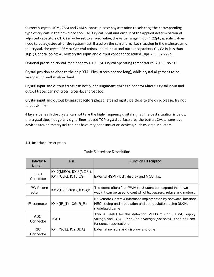
4.4. Interface Description
Table 6 Interface Description
Interface Name
Pin Function Description
HSPI Connector
IO12(MISO), IO13(MOSI), IO14(CLK), IO15(CS) External 4SPI Flash, display and MCU like.
PWMconnector IO12(R), IO15(G),IO13(B) The demo offers four PWM (to 8 users can expand their own
way), it can be used to control lights, buzzers, relays and motors.
IRconnector IO14(IR_T), IO5(IR_R) IR Remote Control4 interfaces implemented by software, interface NEC coding and modulation and demodulation, using 38KHz modulated carrier.
ADC Connector TOUT
This is useful for the detection VDD3P3 (Pin3, Pin4) supply voltage and TOUT (Pin6) input voltage (not both). It can be used for sensor applications.
I2C Connector
IO14(SCL), IO2(SDA) External sensors and displays and other

UART Connector
UART0: TXD(U0TXD),
RXD(U0RXD), IO15(RTS), IO13(CTS)
UART1: IO2(TXD)
May be devices, external UART interface.
Download: U0TXD + U0RXD or GPIO2 + U0RXD
Communication (UART0): U0TXD, U0RXD, MTDO (U0RTS), MTCK (U0CTS) Debug: UART1_TXD (GPIO2) can be used as a print debug information. UART0 default on ESP8266EX power output will be some printed information. This sensitive applications, you can use the internal UART pin swapping function in initialization time, will U0TXD, U0RXD were exchanged with U0RTS, U0CTS. Admiral MTDO MTCK hardware connected to the corresponding external MCU serialconnector to communicate.
I2S接口
I2S Enter:
IO12 (I2SI_DATA) ;
IO13 (I2SI_BCK );
IO14 (I2SI_WS); Use main audio capture, processing and transmission. I2S Export:
IO15 (I2SO_BCK );
IO3 (I2SO_DATA);
IO2 (I2SO_WS ).
4.5. Maximum Ratings
RATINGS Condition Value Unit
Storage temperature 40 to 125
Maximum soldering temperature 260
Supply voltage IPC/JEDEC JSTD020
+3.0 to +3.6 V

4.6. The recommendations of the working environment
Working environment Name Min Average Maximum Unit
Operating temperature 40 20 125
Supply voltage VDD 3.0 3.3 3.6 V
4.7 Digital Port Characteristics
Endconnector Typical values Min Average Maximum Unit
Input logic level low VIL 0.3 0.25VDD V
Input logic level ADVANCED
VIH 0.75VDD VDD+0.3 V
Output logic level low VOL N 0.1VDD V
Output Logic Level ADVANCED VOH 0.8VDD N V
Note: Unless otherwise specified, the test conditions: VDD = 3.3 V, temperature is 20 .
5. RF parameters
Description Min Average Maximum Unit
Input Frequency 2400 2483.5 MHz
Input impedance value 50 ohm
Enter the reflectance values 10 dB
PA output power of 72.2 Mbps 15.5 16.5 17.5 dBm
11b mode at PA output power 19.5 20.5 21.5 dBm

Receiver sensitivity
CCK, 1 Mbps 98 dBm
CCK, 11 Mbps 91 dBm
6 Mbps (1/2 BPSK) 93 dBm
54 Mbps (3/4 64QAM) 75 dBm
HT20, MCS7 (65 Mbps, 72.2 Mbps) 72 dBm
Adjacent suppression
OFDM, 6 Mbps 37 dB
OFDM, 54 Mbps 21 dB
HT20, MCS0 37 dB
HT20, MCS7 20 dB
6. Power
The following data is based on a 3.3V power supply, ambient temperature of 25 ° C, and measured
using the internal regulator.
[1] All measurements were carried out at no SAW filter, the antenna interface is complete.
[2] all transmit data based on a 90% duty cycle, continuous transmission mode at measured.
Table 11 Power
Mode Min Average Maximum Unit
Transfer 802.11b, CCK 11Mbps, POUT=+17dBm
170 mA
Transfer 802.11g, OFDM 54Mbps, POUT =+15dBm
140 mA
Transfer 802.11n, MCS7, POUT =+13dBm 120 mA
Receiving 802.11b, packet length of 1024 bytes, 80dBm
50 mA
Receiving 802.11g, packet length of 1024 bytes, 70dBm
56 mA

Receiving 802.11n, packet length of 1024 bytes, 65dBm
56 mA
ModemSleep① 15 mA
LightSleep② 0.9 mA
DeepSleep③ 10 uA
Power Off 0.5 uA
Note ①: Modem-Sleep Use to require CPU has been in working condition, such as PWM or I2S should
use, etc. In keeping WiFi connection, if no data transmission, according to the 802.11 standard (such
as U-APSD), turn off WiFi Modem circuit power. For example, in DTIM3, each sleep 300mS, wake 3mS
received the Beacon AP packages, etc., the overall average current of about 15mA.
Note ②: Light-Sleep may be suspended for the CPU applications such as WiFi switch. In keeping WiFi
connection, if no data transmission, according to the 802.11 standard (such as U-APSD), closed circuit
and pause WiFi Modem CPU to save power. For example, in DTIM3, each sleep 300 ms, wake 3ms
received the Beacon AP packages, etc., the overall average current of approximately 0.9 mA.
Note ③: Deep-Sleep has remained without a WiFi connection, long time to send a packet of
applications, such as 一 second temperature sensor measurements every 100 seconds. For example,
every 300 s after waking need 0.3s - 1s even send data on AP, the overall average current can be far
less than 1mA.
7. tilt warming
Table 12 tilt warming
Tilt the maximum temperature TS TL Preheat Maximum of 3 / sec
The minimum temperature value (TS Min.) Typical temperatures (TS Typ.) Temperature value is largest (TS Max.) Time (TS)
150 175 200 60~180秒
Tilt temperature (TL to TP) Maximum of 3 / sec
Duration / temperature (TL) / time (TL) 217/60~150秒
Peak temperature (TP) Maximum temperature 260 , sustained 10 seconds

Target temperature peak (TP target) 260+0/5
Actual peak (tP) 5 Duration 20~40秒
Tilt cooling Maximum 6 / sec
Time (t) from the desired peak temperature was adjusted to 25 Maximum 8 minutes
8. Schematic
Figure 5 ESP-12F Schematic

9. Product Trial
(1) Taobao shop: Shenzhen Shun Technology Co., Ltd. may
(2) micro-channel public number
(3) Technical Support E-mail: [email protected]