Embed Size (px)
Citation preview

ESP32-WROVER Datasheet
Espressif Systems
September 8, 2017

About This Guide
This document provides the specifications for the ESP32-WROVER module.
The document structure is as follows:
Chapter Title Subject
Chapter 1 Preface An overview of ESP32-WROVER
Chapter 2 Pin Definitions Device pinout and pin descriptions
Chapter 3 Functional Description Description of major functional modules
Chapter 4 Peripherals and Sensors Description of peripherals.
Chapter 5 Electrical Characteristics Electrical characteristics and specifications of ESP32-WROVER
Chapter 6 Schematics The schematics of ESP32-WROVER
Chapter 7 Peripheral Schematics The peripheral schematics of ESP32-WROVER
Chapter 8 Dimensions The dimensions of ESP32-WROVER
Chapter 8 Learning Resources ESP32-related must-read materials and must-have resources
Release Notes
Date Version Release notes
2017.08 V1.0 First release
2017.09 V1.1
Updated Section 2.1Pin Layout;
Updated the ESP32-WROVER Schematics and dded a note in Chapter 7;
Added Chapter 8 Dimensions.
Documentation Change Notification
Espressif provides email notifications to keep customers updated on changes to technical documentation.
Please subscribe here.
Certificates
Download certificates for Espressif products from here.
Disclaimer and Copyright Notice
Information in this document, including URL references, is subject to change without notice. THIS DOCUMENT IS
PROVIDED AS IS WITH NO WARRANTIES WHATSOEVER, INCLUDING ANY WARRANTY OF MERCHANTABIL-
ITY, NON-INFRINGEMENT, FITNESS FOR ANY PARTICULAR PURPOSE, OR ANY WARRANTY OTHERWISE
ARISING OUT OF ANY PROPOSAL, SPECIFICATION OR SAMPLE.
All liability, including liability for infringement of any proprietary rights, relating to use of information in this docu-
ment is disclaimed. No licenses express or implied, by estoppel or otherwise, to any intellectual property rights
are granted herein. The Wi-Fi Alliance Member logo is a trademark of the Wi-Fi Alliance. The Bluetooth logo is a
registered trademark of Bluetooth SIG.
All trade names, trademarks and registered trademarks mentioned in this document are property of their respective
owners, and are hereby acknowledged.
Copyright © 2017 Espressif Inc. All rights reserved.

Contents
1 Overview 1
2 Pin Definitions 3
2.1 Pin Layout 3
2.2 Pin Description 4
2.3 Strapping Pins 5
3 Functional Description 7
3.1 CPU and Internal Memory 7
3.2 External Flash and SRAM 7
3.3 Crystal Oscillators 7
3.4 RTC and Low-Power Management 8
4 Peripherals and Sensors 10
4.1 Peripherals and Sensors Description 10
5 Electrical Characteristics 15
5.1 Absolute Maximum Ratings 15
5.2 Wi-Fi Radio 15
5.3 BLE Radio 16
5.3.1 Receiver 16
5.3.2 Transmitter 16
5.4 Reflow Profile 17
6 Schematics 18
7 Peripheral Schematics 19
8 Dimensions 20
9 Learning Resources 21
9.1 Must-Read Documents 21
9.2 Must-Have Resources 21

List of Tables1 ESP32-WROVER Specifications 1
2 Pin Definitions 4
3 Strapping Pins 5
4 Functionalities Depending on the Power Modes 8
5 Power Consumption by Power Modes 8
6 Description of Peripherals and Sensors 10
7 Absolute Maximum Ratings 15
8 Wi-Fi Radio Characteristics 15
9 Receiver Characteristics — BLE 16
10 Transmitter Characteristics — BLE 16

List of Figures1 ESP32-WROVER Pin Layout 3
2 Reflow Profile 17
3 ESP32-WROVER Schematics 18
4 ESP32-WROVER Peripheral Schematics 19
5 ESP32-WROVER Dimensions 20

1. OVERVIEW
1. Overview
ESP32-WROVER is a powerful, generic WiFi-BT-BLE MCU module that targets a wide variety of applications,
ranging from low-power sensor networks to the most demanding tasks, such as voice encoding, music streaming
and MP3 decoding.
At the core of this module is the ESP32-D0WDQ6 chip*, same as ESP-WROOM-32 module. Compared to ESP-
WROOM-32, ESP32-WROVER has an additional SPI Pseudo static RAM (PSRAM) of 32 Mbits. As such, ESP32-
WROVER features both 4 MB external SPI flash and 4 MB external PSRAM.
The ESP32-WROVER module has a PCB antenna, while the ESP32-WROVER-I uses an IPEX antenna. The
information in this datasheet is applicable to both of the two modules.
The chip embedded is designed to be scalable and adaptive. There are two CPU cores that can be individually
controlled, and the clock frequency is adjustable from 80 MHz to 240 MHz. The user may also power off the
CPU and make use of the low-power co-processor to constantly monitor the peripherals for changes or crossing
of thresholds. ESP32 integrates a rich set of peripherals, ranging from capacitive touch sensors, Hall sensors,
low-noise sense amplifiers, SD card interface, Ethernet, high-speed SPI, UART, I2S and I2C.
Note:
* For details on the part number of the ESP32 series, please refer to the document ESP32 Datasheet.
The integration of Bluetooth, Bluetooth LE and Wi-Fi ensures that a wide range of applications can be targeted,
and that the module is future proof: using Wi-Fi allows a large physical range and direct connection to the internet
through a Wi-Fi router, while using Bluetooth allows the user to conveniently connect to the phone or broadcast
low energy beacons for its detection. The sleep current of the ESP32 chip is less than 5 µA, making it suitable
for battery powered and wearable electronics applications. ESP32 supports a data rate of up to 150 Mbps,
and 20.5 dBm output power at the antenna to ensure the widest physical range. As such the chip does offer
industry-leading specifications and the best performance for electronic integration, range, power consumption,
and connectivity.
The operating system chosen for ESP32 is freeRTOS with LwIP; TLS 1.2 with hardware acceleration is built in as
well. Secure (encrypted) over the air (OTA) upgrade is also supported, so that developers can continually upgrade
their products even after their release.
Table 1 provides the specifications of ESP32-WROVER.
Table 1: ESP32-WROVER Specifications
Categories Items Specifications
Wi-Fi
RF certification FCC/CE-RED/SRRC
Protocols
802.11 b/g/n/e/i (802.11n up to 150 Mbps)
A-MPDU and A-MSDU aggregation and 0.4 µs guard in-
terval support
Frequency range 2.4 GHz ~ 2.5 GHz
Espressif Systems 1 ESP32-WROVER Datasheet V1.1

1. OVERVIEW
Categories Items Specifications
Bluetooth
Protocols Bluetooth v4.2 BR/EDR and BLE specification
Radio
NZIF receiver with -97 dBm sensitivity
Class-1, class-2 and class-3 transmitter
AFH
Audio CVSD and SBC
Hardware
Module interface
SD card, UART, SPI, SDIO, I2C, LED PWM, Motor PWM,
I2S, IR
GPIO, capacitive touch sensor, ADC, DAC, LNA pre-
amplier
On-chip sensor Hall sensor, temperature sensor
On-board clock 40 MHz crystal
Operating voltage/Power supply 2.3 ~ 3.6V
Operating current Average: 80 mA
Minimum current delivered by
power supply500 mA
Operating temperature range -40°C ~ 85°C
Ambient temperature range Normal temperature
Package size 18±0.2 mm x 31.4±0.2 mm x 3.3±0.15 mm
Software
Wi-Fi mode Station/SoftAP/SoftAP+Station/P2P
Security WPA/WPA2/WPA2-Enterprise/WPS
Encryption AES/RSA/ECC/SHA
Firmware upgradeUART Download / OTA (via network) / download and write
firmware via host
Software developmentSupports Cloud Server Development / SDK for custom
firmware development
Network protocols IPv4, IPv6, SSL, TCP/UDP/HTTP/FTP/MQTT
User configuration AT instruction set, cloud server, Android/iOS app
Espressif Systems 2 ESP32-WROVER Datasheet V1.1

2. PIN DEFINITIONS
2. Pin Definitions
2.1 Pin Layout
Keepout Zone
VDD33
EN
IO14
IO12
IO33
IO25
IO26
IO27
GND
IO32
IO35
IO34
SENSOR_VN
SENSOR_VP
37
36
26
25
30
29
28
27
38
31
32
33
34
35
IO23
IO22
IO4
IO0
IO18
IO5
NC
NC
GND
IO19
NC
IO21
RXD0
TXD0
39:GND
3
13
14
9
10
11
12
8
7
6
5
4
15
16
17
18
IO13
GND
CMD
SD3
SD2
IO2
SD1
SD0
CLK
IO15
1
2
19
24
23
22
21
20
Figure 1: ESP32-WROVER Pin Layout
Espressif Systems 3 ESP32-WROVER Datasheet V1.1

2. PIN DEFINITIONS
2.2 Pin Description
ESP32-WROVER has 38 pins. See pin definitions in Table 2.
Table 2: Pin Definitions
Name No. Type Function
GND 1 P Ground
3V3 2 P Power supply.
EN 3 I Chip-enable signal. Active high.
SENSOR_VP 4 I GPIO36, SENSOR_VP, ADC_H, ADC1_CH0, RTC_GPIO0
SENSOR_VN 5 I GPIO39, SENSOR_VN, ADC1_CH3, ADC_H, RTC_GPIO3
IO34 6 I GPIO34, ADC1_CH6, RTC_GPIO4
IO35 7 I GPIO35, ADC1_CH7, RTC_GPIO5
IO32 8 I/OGPIO32, XTAL_32K_P (32.768 kHz crystal oscillator input), ADC1_CH4,
TOUCH9, RTC_GPIO9
IO33 9 I/OGPIO33, XTAL_32K_N (32.768 kHz crystal oscillator output), ADC1_CH5,
TOUCH8, RTC_GPIO8
IO25 10 I/O GPIO25, DAC_1, ADC2_CH8, RTC_GPIO6, EMAC_RXD0
IO26 11 I/O GPIO26, DAC_2, ADC2_CH9, RTC_GPIO7, EMAC_RXD1
IO27 12 I/O GPIO27, ADC2_CH7, TOUCH7, RTC_GPIO17, EMAC_RX_DV
IO14 13 I/OGPIO14, ADC2_CH6, TOUCH6, RTC_GPIO16, MTMS, HSPICLK,
HS2_CLK, SD_CLK, EMAC_TXD2
IO12 14 I/OGPIO12, ADC2_CH5, TOUCH5, RTC_GPIO15, MTDI, HSPIQ,
HS2_DATA2, SD_DATA2, EMAC_TXD3
GND 15 P Ground
IO13 16 I/OGPIO13, ADC2_CH4, TOUCH4, RTC_GPIO14, MTCK, HSPID,
HS2_DATA3, SD_DATA3, EMAC_RX_ER
SHD/SD2* 17 I/O GPIO9, SD_DATA2, SPIHD, HS1_DATA2, U1RXD
SWP/SD3* 18 I/O GPIO10, SD_DATA3, SPIWP, HS1_DATA3, U1TXD
SCS/CMD* 19 I/O GPIO11, SD_CMD, SPICS0, HS1_CMD, U1RTS
SCK/CLK* 20 I/O GPIO6, SD_CLK, SPICLK, HS1_CLK, U1CTS
SDO/SD0* 21 I/O GPIO7, SD_DATA0, SPIQ, HS1_DATA0, U2RTS
SDI/SD1* 22 I/O GPIO8, SD_DATA1, SPID, HS1_DATA1, U2CTS
IO15 23 I/OGPIO15, ADC2_CH3, TOUCH3, MTDO, HSPICS0, RTC_GPIO13,
HS2_CMD, SD_CMD, EMAC_RXD3
IO2 24 I/OGPIO2, ADC2_CH2, TOUCH2, RTC_GPIO12, HSPIWP, HS2_DATA0,
SD_DATA0
IO0 25 I/OGPIO0, ADC2_CH1, TOUCH1, RTC_GPIO11, CLK_OUT1,
EMAC_TX_CLK
IO4 26 I/OGPIO4, ADC2_CH0, TOUCH0, RTC_GPIO10, HSPIHD, HS2_DATA1,
SD_DATA1, EMAC_TX_ER
IO16 27 I/O GPIO16, HS1_DATA4, U2RXD, EMAC_CLK_OUT
IO17 28 I/O GPIO17, HS1_DATA5, U2TXD, EMAC_CLK_OUT_180
IO5 29 I/O GPIO5, VSPICS0, HS1_DATA6, EMAC_RX_CLK
IO18 30 I/O GPIO18, VSPICLK, HS1_DATA7
IO19 31 I/O GPIO19, VSPIQ, U0CTS, EMAC_TXD0
Espressif Systems 4 ESP32-WROVER Datasheet V1.1

2. PIN DEFINITIONS
Name No. Type Function
NC 32 - -
IO21 33 I/O GPIO21, VSPIHD, EMAC_TX_EN
RXD0 34 I/O GPIO3, U0RXD, CLK_OUT2
TXD0 35 I/O GPIO1, U0TXD, CLK_OUT3, EMAC_RXD2
IO22 36 I/O GPIO22, VSPIWP, U0RTS, EMAC_TXD1
IO23 37 I/O GPIO23, VSPID, HS1_STROBE
GND 38 P Ground
2.3 Strapping Pins
Please refer to Chapter 6 ESP32-WROVER schematics. ESP32 has five strapping pins, which can be seen in
Section 6 Schematics:
• MTDI
• GPIO0
• GPIO2
• MTDO
• GPIO5
Software can read the value of these five bits from the register ”GPIO_STRAPPING”.
During the chip power-on reset, the latches of the strapping pins sample the voltage level as strapping bits of ”0”
or ”1”, and hold these bits until the chip is powered down or shut down. The strapping bits configure the device
boot mode, the operating voltage of VDD_SDIO and other system initial settings.
Each strapping pin is connected with its internal pull-up/pull-down during the chip reset. Consequently, if a strap-
ping pin is unconnected or the connected external circuit is high-impendence, the internal weak pull-up/pull-down
will determine the default input level of the strapping pins.
To change the strapping bit values, users can apply the external pull-down/pull-up resistances, or apply the host
MCU’s GPIOs to control the voltage level of these pins when powering on ESP32.
After reset, the strapping pins work as the normal functions pins.
Refer to Table 3 for detailed boot modes’ configuration by strapping pins.
Table 3: Strapping Pins
Voltage of Internal LDO (VDD_SDIO)
Pin Default 3.3V 1.8V
MTDI Pull-down 0 1
Booting Mode
Pin Default SPI Boot Download Boot
GPIO0 Pull-up 1 0
GPIO2 Pull-down Don’t-care 0
Debugging Log on U0TXD During Booting
Pin Default U0TXD Toggling U0TXD Silent
MTDO Pull-up 1 0
Espressif Systems 5 ESP32-WROVER Datasheet V1.1

2. PIN DEFINITIONS
Timing of SDIO Slave
Pin DefaultFalling-edge Input
Falling-edge Output
Falling-edge Input
Rising-edge Output
Rising-edge Input
Falling-edge Output
Rising-edge Input
Rising-edge Output
MTDO Pull-up 0 0 1 1
GPIO5 Pull-up 0 1 0 1
Note:
• Firmware can configure register bits to change the settings of ”Voltage of Internal LDO (VDD_SDIO)” and ”Timing
of SDIO Slave” after booting.
• The MTDI is internally pulled high in the module, as the flash and SRAM in ESP32-WROVER only support a power
voltage of 1.8V (output by VDD_SDIO).
Espressif Systems 6 ESP32-WROVER Datasheet V1.1

3. FUNCTIONAL DESCRIPTION
3. Functional Description
This chapter describes the modules and functions integrated in ESP32-WROVER.
3.1 CPU and Internal Memory
ESP32-D0WDQ6 contains two low-power Xtensa® 32-bit LX6 microprocessors. The internal memory includes:
• 448 KB of ROM for booting and core functions.
• 520 KB (8 KB RTC FAST Memory included) of on-chip SRAM for data and instruction.
– 8 KB of SRAM in RTC, which is called RTC FAST Memory and can be used for data storage; it is
accessed by the main CPU during RTC Boot from the Deep-sleep mode.
• 8 KB of SRAM in RTC, which is called RTC SLOW Memory and can be accessed by the co-processor during
the Deep-sleep mode.
• 1 kbit of eFuse, of which 256 bits are used for the system (MAC address and chip configuration) and the
remaining 768 bits are reserved for customer applications, including Flash-Encryption and Chip-ID.
3.2 External Flash and SRAM
ESP32 supports up to four 16-MB of external QSPI flash and SRAM with hardware encryption based on AES to
protect developers’ programs and data.
ESP32 can access the external QSPI flash and SRAM through high-speed caches.
• Up to 16 MB of external flash are memory-mapped onto the CPU code space, supporting 8, 16 and 32-bit
access. Code execution is supported.
• Up to 8 MB of external flash/SRAM are memory-mapped onto the CPU data space, supporting 8, 16 and
32-bit access. Data-read is supported on the flash and SRAM. Data-write is supported on the SRAM.
ESP32-WROVER integrates 4 MB of external SPI flash. The 4-MB SPI flash can be memory-mapped onto the
CPU code space, supporting 8, 16 and 32-bit access. Code execution is supported.
In addition to the 4 MB SPI flash, ESP32-WROVER also integrates 4 MB PSRAM for more memory space.
3.3 Crystal Oscillators
The ESP32 Wi-Fi/BT firmware can only support 40 MHz crystal oscillator for now.
Espressif Systems 7 ESP32-WROVER Datasheet V1.1

3. FUNCTIONAL DESCRIPTION
3.4 RTC and Low-Power Management
With the use of advanced power management technologies, ESP32 can switch between different power modes
(see Table 4).
• Power modes
– Active mode: The chip radio is powered on. The chip can receive, transmit, or listen.
– Modem-sleep mode: The CPU is operational and the clock is configurable. The Wi-Fi/Bluetooth base-
band and radio are disabled.
– Light-sleep mode: The CPU is paused. The RTC memory and RTC peripherals, as well as the ULP
co-processor are running. Any wake-up events (MAC, host, RTC timer, or external interrupts) will wake
up the chip.
– Deep-sleep mode: Only the RTC memory and RTC peripherals are powered on. Wi-Fi and Bluetooth
connection data are stored in the RTC memory. The ULP co-processor can work.
– Hibernation mode: The internal 8-MHz oscillator and ULP co-processor are disabled. The RTC recovery
memory is powered down. Only one RTC timer on the slow clock and some RTC GPIOs are active.
The RTC timer or the RTC GPIOs can wake up the chip from the Hibernation mode.
• Sleep Patterns
– Association sleep pattern: The power mode switches between the Active mode, Modem- and Light-
sleep mode during this sleep pattern. The CPU, Wi-Fi, Bluetooth, and radio are woken up at predeter-
mined intervals to keep Wi-Fi/BT connections alive.
– ULP sensor-monitored pattern: The main CPU is in the Deep-sleep mode. The ULP co-processor takes
sensor measurements and wakes up the main system, based on the data collected from sensors.
Table 4: Functionalities Depending on the Power Modes
Power mode Active Modem-sleep Light-sleep Deep-sleep Hibernation
Sleep pattern Association sleep patternULP sensor-
monitored pattern-
CPU ON ON PAUSE OFF OFF
Wi-Fi/BT baseband and radio ON OFF OFF OFF OFF
RTC memory and RTC pe-
ripheralsON ON ON ON OFF
ULP co-processor ON ON ON ON/OFF OFF
The power consumption varies with different power modes/sleep patterns and work statuses of functional modules.
Please see Table 5 for details.
Table 5: Power Consumption by Power Modes
Power mode Description Power consumption
Active (RF working)
Wi-Fi Tx packet 14 dBm ~ 19.5 dBm
Please refer to ESP32 Datasheet.Wi-Fi / BT Tx packet 0 dBm
Wi-Fi / BT Rx and listening
Association sleep pattern (by Light-sleep) 1 mA ~ 4 mA @DTIM3
Espressif Systems 8 ESP32-WROVER Datasheet V1.1

3. FUNCTIONAL DESCRIPTION
Power mode Description Power consumption
Modem-sleep The CPU is powered on.
Max speed 240 MHz: 30 mA ~ 50 mA
Normal speed 80 MHz: 20 mA ~ 25 mA
Slow speed 2 MHz: 2 mA ~ 4 mA
Light-sleep - 0.8 mA
Deep-sleep
The ULP co-processor is powered on. 150 µA
ULP sensor-monitored pattern 100 µA @1% duty
RTC timer + RTC memory 10 µA
Hibernation RTC timer only 5 µA
Power off CHIP_PU is set to low level, the chip is powered off 0.1 µA
Note:
• During Deep-sleep, when the ULP co-processor is powered on, peripherals such as GPIO and I2C are able to
work.
• When the system works in the ULP sensor-monitored pattern, the ULP co-processor works with the ULP sensor
periodically; ADC works with a duty cycle of 1%, so the power consumption is 100 µA.
Espressif Systems 9 ESP32-WROVER Datasheet V1.1

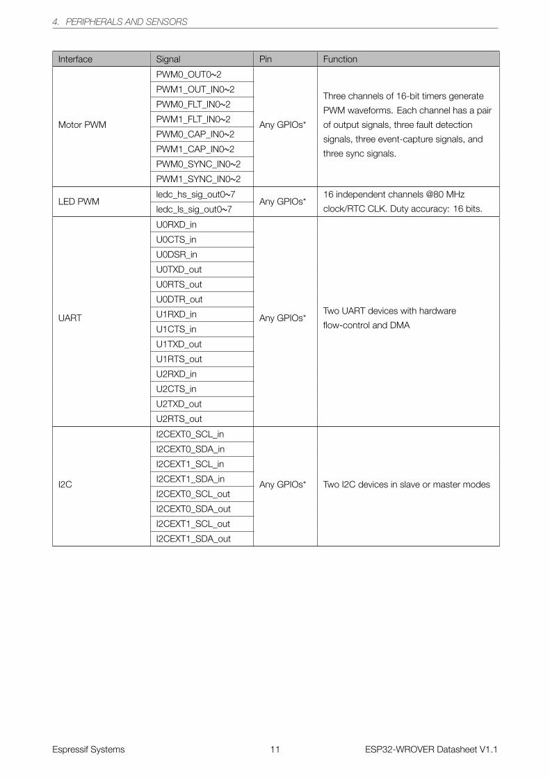
4. PERIPHERALS AND SENSORS
4. Peripherals and Sensors
4.1 Peripherals and Sensors Description
Table 6: Description of Peripherals and Sensors
Interface Signal Pin Function
ADC
ADC1_CH0 SENSOR_VP
Two 12-bit SAR ADCs
ADC1_CH3 SENSOR_VN
ADC1_CH4 IO32
ADC1_CH5 IO33
ADC1_CH6 IO34
ADC1_CH7 IO35
ADC2_CH0 IO4
ADC2_CH1 IO0
ADC2_CH2 IO2
ADC2_CH3 IO15
ADC2_CH4 IO13
ADC2_CH5 IO12
ADC2_CH6 IO14
ADC2_CH7 IO27
ADC2_CH8 IO25
ADC2_CH9 IO26
Ultra-Low Noise
Analog Pre-Amplifier
SENSOR_VP IO36 Provides about 60 dB gain by using larger
capacitors on PCBSENSOR_VN IO39
DACDAC_1 IO25
Two 8-bit DACsDAC_2 IO26
Touch Sensor
TOUCH0 IO4
Capacitive touch sensors
TOUCH1 IO0
TOUCH2 IO2
TOUCH3 IO15
TOUCH4 IO13
TOUCH5 IO12
TOUCH6 IO14
TOUCH7 IO27
TOUCH8 IO33
TOUCH9 IO32
SD/SDIO/MMC Host
Controller
HS2_CLK MTMS
Supports SD memory card V3.01 standard
HS2_CMD MTDO
HS2_DATA0 IO2
HS2_DATA1 IO4
HS2_DATA2 MTDI
HS2_DATA3 MTCK
Espressif Systems 10 ESP32-WROVER Datasheet V1.1
4. PERIPHERALS AND SENSORS
Interface Signal Pin Function
Motor PWM
PWM0_OUT0~2
Any GPIOs*
Three channels of 16-bit timers generate
PWM waveforms. Each channel has a pair
of output signals, three fault detection
signals, three event-capture signals, and
three sync signals.
PWM1_OUT_IN0~2
PWM0_FLT_IN0~2
PWM1_FLT_IN0~2
PWM0_CAP_IN0~2
PWM1_CAP_IN0~2
PWM0_SYNC_IN0~2
PWM1_SYNC_IN0~2
LED PWMledc_hs_sig_out0~7
Any GPIOs*16 independent channels @80 MHz
clock/RTC CLK. Duty accuracy: 16 bits.ledc_ls_sig_out0~7
UART
U0RXD_in
Any GPIOs*Two UART devices with hardware
flow-control and DMA
U0CTS_in
U0DSR_in
U0TXD_out
U0RTS_out
U0DTR_out
U1RXD_in
U1CTS_in
U1TXD_out
U1RTS_out
U2RXD_in
U2CTS_in
U2TXD_out
U2RTS_out
I2C
I2CEXT0_SCL_in
Any GPIOs* Two I2C devices in slave or master modes
I2CEXT0_SDA_in
I2CEXT1_SCL_in
I2CEXT1_SDA_in
I2CEXT0_SCL_out
I2CEXT0_SDA_out
I2CEXT1_SCL_out
I2CEXT1_SDA_out
Espressif Systems 11 ESP32-WROVER Datasheet V1.1

4. PERIPHERALS AND SENSORS
Interface Signal Pin Function
I2S
I2S0I_DATA_in0~15
Any GPIOs*Stereo input and output from/to the audio
codec, and parallel LCD data output
I2S0O_BCK_in
I2S0O_WS_in
I2S0I_BCK_in
I2S0I_WS_in
I2S0I_H_SYNC
I2S0I_V_SYNC
I2S0I_H_ENABLE
I2S0O_BCK_out
I2S0O_WS_out
I2S0I_BCK_out
I2S0I_WS_out
I2S0O_DATA_out0~23
I2S1I_DATA_in0~15
I2S1O_BCK_in
I2S1O_WS_in
I2S1I_BCK_in
I2S1I_WS_in
I2S1I_H_SYNC
I2S1I_V_SYNC
I2S1I_H_ENABLE
I2S1O_BCK_out
I2S1O_WS_out
I2S1I_BCK_out
I2S1I_WS_out
I2S1O_DATA_out0~23
Remote ControllerRMT_SIG_IN0~7
Any GPIOs*Eight channels of IR transmitter and
receiver for various waveformsRMT_SIG_OUT0~7
Espressif Systems 12 ESP32-WROVER Datasheet V1.1

4. PERIPHERALS AND SENSORS
Interface Signal Pin Function
Parallel QSPI
SPIHD SHD/SD2
Supports Standard SPI, Dual SPI, and
Quad SPI that can be connected to the
external flash and SRAM
SPIWP SWP/SD3
SPICS0 SCS/CMD
SPICLK SCK/CLK
SPIQ SDO/SD0
SPID SDI/SD1
HSPICLK IO14
HSPICS0 IO15
HSPIQ IO12
HSPID IO13
HSPIHD IO4
HSPIWP IO2
VSPICLK IO18
VSPICS0 IO5
VSPIQ IO19
VSPID IO23
VSPIHD IO21
VSPIWP IO22
General Purpose
SPI
HSPIQ_in/_out
Any GPIOs*
Standard SPI consists of clock,
chip-select, MOSI and MISO. These SPIs
can be connected to LCD and other
external devices. They support the
following features:
• both master and slave modes;
• 4 sub-modes of the SPI format
transfer that depend on the clock
phase (CPHA) and clock polarity
(CPOL) control;
• configurable SPI frequency;
• up to 64 bytes of FIFO and DMA.
HSPID_in/_out
HSPICLK_in/_out
HSPI_CS0_in/_out
HSPI_CS1_out
HSPI_CS2_out
VSPIQ_in/_out
VSPID_in/_out
VSPICLK_in/_out
VSPI_CS0_in/_out
VSPI_CS1_out
VSPI_CS2_out
JTAG
MTDI IO12
JTAG for software debuggingMTCK IO13
MTMS IO14
MTDO IO15
Espressif Systems 13 ESP32-WROVER Datasheet V1.1

4. PERIPHERALS AND SENSORS
Interface Signal Pin Function
SDIO Slave
SD_CLK IO6
SDIO interface that conforms to the
industry standard SDIO 2.0 card
specification.
SD_CMD IO11
SD_DATA0 IO7
SD_DATA1 IO8
SD_DATA2 IO9
SD_DATA3 IO10
EMAC
EMAC_TX_CLK IO0
Ethernet MAC with MII/RMII interface
EMAC_RX_CLK IO5
EMAC_TX_EN IO21
EMAC_TXD0 IO19
EMAC_TXD1 IO22
EMAC_TXD2 IO14
EMAC_TXD3 IO12
EMAC_RX_ER IO13
EMAC_RX_DV IO27
EMAC_RXD0 IO25
EMAC_RXD1 IO26
EMAC_RXD2 TXD0
EMAC_RXD3 IO15
EMAC_CLK_OUT IO16
EMAC_CLK_OUT_180 IO17
EMAC_TX_ER IO4
EMAC_MDC_out Any GPIOs*
EMAC_MDI_in Any GPIOs*
EMAC_MDO_out Any GPIOs*
EMAC_CRS_out Any GPIOs*
EMAC_COL_out Any GPIOs*
Note:
Functions of Motor PWM, LED PWM, UART, I2C, I2S, general purpose SPI and Remote Controller can be configured to
any GPIO.
Espressif Systems 14 ESP32-WROVER Datasheet V1.1

5. ELECTRICAL CHARACTERISTICS
5. Electrical Characteristics
Note:
The specifications in this chapter have been tested under the following general condition: VDD = 3.3V, TA = 27°C, unless
otherwise specified.
5.1 Absolute Maximum Ratings
Table 7: Absolute Maximum Ratings
Parameter Symbol Min Typ Max Unit
Power supply VDD 2.3 3.3 3.6 V
Minimum current delivered by
power supplyIV DD 0.5 - - A
Input low voltage VIL -0.3 - 0.25×VIO1 V
Input high voltage VIH 0.75×VIO1 - VIO
1+0.3 V
Input leakage current IIL - - 50 nA
Input pin capacitance Cpad - - 2 pF
Output low voltage VOL - - 0.1×VIO1 V
Output high voltage VOH 0.8×VIO1 - - V
Maximum output drive capability IMAX - - 40 mA
Storage temperature range TSTR -40 - 85 °C
Operating temperature range TOPR -40 - 85 °C
1. VIO is the power supply for a specific pad. More details can be found in the ESP32 Datasheet, Appendix IO_MUX. Forexample, the power supply for SD_CLK is the VDD_SDIO.
5.2 Wi-Fi Radio
Table 8: Wi-Fi Radio Characteristics
Description Min Typical Max Unit
Input frequency 2412 - 2484 MHz
Output impedance - 30+j10 - Ω
Input reflection - - -10 dB
Tx power
Output power of PA for 72.2 Mbps 13 14 15 dBm
Output power of PA for 11b mode 19.5 20 20.5 dBm
Sensitivity
DSSS, 1 Mbps - -98 - dBm
CCK, 11 Mbps - -91 - dBm
OFDM, 6 Mbps - -93 - dBm
OFDM, 54 Mbps - -75 - dBm
HT20, MCS0 - -93 - dBm
Espressif Systems 15 ESP32-WROVER Datasheet V1.1

5. ELECTRICAL CHARACTERISTICS
Description Min Typical Max Unit
HT20, MCS7 - -73 - dBm
HT40, MCS0 - -90 - dBm
HT40, MCS7 - -70 - dBm
MCS32 - -89 - dBm
Adjacent channel rejection
OFDM, 6 Mbps - 37 - dB
OFDM, 54 Mbps - 21 - dB
HT20, MCS0 - 37 - dB
HT20, MCS7 - 20 - dB
5.3 BLE Radio
5.3.1 Receiver
Table 9: Receiver Characteristics — BLE
Parameter Conditions Min Typ Max Unit
Sensitivity @30.8% PER - - -97 - dBm
Maximum received signal @30.8% PER - 0 - - dBm
Co-channel C/I - - +10 - dB
Adjacent channel selectivity C/I
F = F0 + 1 MHz - -5 - dB
F = F0 - 1 MHz - -5 - dB
F = F0 + 2 MHz - -25 - dB
F = F0 - 2 MHz - -35 - dB
F = F0 + 3 MHz - -25 - dB
F = F0 - 3 MHz - -45 - dB
Out-of-band blocking performance
30 MHz ~ 2000 MHz -10 - - dBm
2000 MHz ~ 2400 MHz -27 - - dBm
2500 MHz ~ 3000 MHz -27 - - dBm
3000 MHz ~ 12.5 GHz -10 - - dBm
Intermodulation - -36 - - dBm
5.3.2 Transmitter
Table 10: Transmitter Characteristics — BLE
Parameter Conditions Min Typ Max Unit
RF transmit power - - 0 - dBm
Gain control step - - ±3 - dBm
RF power control range - -12 - +12 dBm
Espressif Systems 16 ESP32-WROVER Datasheet V1.1

5. ELECTRICAL CHARACTERISTICS
Parameter Conditions Min Typ Max Unit
Adjacent channel transmit power
F = F0 + 1 MHz - -14.6 - dBm
F = F0 - 1 MHz - -12.7 - dBm
F = F0 + 2 MHz - -44.3 - dBm
F = F0 - 2 MHz - -38.7 - dBm
F = F0 + 3 MHz - -49.2 - dBm
F = F0 - 3 MHz - -44.7 - dBm
F = F0 + > 3 MHz - -50 - dBm
F = F0 - > 3 MHz - -50 - dBm
∆ f1avg - - - 265 kHz
∆ f2max - 247 - - kHz
∆ f2avg/∆ f1avg - - -0.92 - -
ICFT - - -10 - kHz
Drift rate - - 0.7 - kHz/50 µs
Drift - - 2 - kHz
5.4 Reflow Profile
Tem
pera
ture
()
Soldering time> 30s
Ramp-up zone
Time (sec.)
50 150
0
25
1 ~ 3/s
0
200
250
200
Peak Temp. 235 ~ 250
3 ~ 5/sCooling down zonePreheating zone
150 ~ 200 60 ~ 120s
100
217
50
100 250
Ramp-up zone — Temp.: <150 Time: 60 ~ 90s Ramp-up rate: 1 ~ 3/sPreheating zone — Temp.: 150 ~ 200 Time: 60 ~ 120s Ramp-up rate: 0.3 ~ 0.8/sReflow soldering zone — Peak Temp.: 235 ~ 250 (<245 recommended) Time: 30 ~ 70sCooling down zone — Temp.: 217 ~ 170 Ramp-down rate: 3 ~ 5/sSolder — Sn&Ag&Cu Lead-free solder (SAC305)
Figure 2: Reflow Profile
Espressif Systems 17 ESP32-WROVER Datasheet V1.1

6.SCHEM
ATIC
S
6. Schematics
GPIO16
SRAM_CLK
SENSOR_VP
SENSOR_VN
GPIO32
GPIO33 GPIO18
GPIO2
U0TXD
U0RXD
GPIO22
GPIO21
GPIO19
SHD/SD2
SWP/SD3
SCS/CMD
FLASH_CLK
SDO/SD0
SDI/SD1
GPIO23
CHIP_PU
GPIO34
GPIO35
GPIO25
GPIO26
GPIO27
GPIO14
GPIO12
GPIO13
GPIO0
GPIO15
GPIO4
GPIO5
FLASH_CLK
SCS/CMD
SHD/SD2 SWP/SD3
SDI/SD1
SDO/SD0
SCK/CLK
GPIO17
FLASH_CLK
SRAM_CLK
SDO/SD0SWP/SD3
SHD/SD2
SDI/SD1
CHIP_PU
GPIO35
SENSOR_VP
SENSOR_VN
GPIO34
GPIO25
GPIO26
GPIO27
GPIO14
GPIO12
GPIO16
SDI/SD1SDO/SD0SCK/CLKSCS/CMDSWP/SD3SHD/SD2
GPIO5GPIO18GPIO23
GPIO17
GPIO15
GPIO13
GPIO2
GPIO0
GPIO4
GPIO32
GPIO33
U0RXDGPIO22
GPIO21
GPIO19
U0TXD
GND
VDD_SDIO
GND GND
VDD33
GND
GND
VDD_SDIO
VDD33
VDD_SDIO
GND
VDD33
GND
GND
VDD_SDIO
GND
GND
VDD33
GND
GND
GND
GND
GNDGND
VDD33
GND
GND
GND
VDD33
VDD33
GND
GND
GND GND
GND
ESP32 Module:with 1.8V Flash & SRAMThe operating voltage for signals marked in blue is 1.8V.
Pin.1GND
Pin.15GND
Pin.38GND
Pin.23V3
Pin.3CHIP_PU/EN
Pin.4SENSOR_VP
Pin.5SENSOR_VN
Pin.6IO34
Pin.7IO35
Pin.8IO32
Pin.9IO33
Pin.10IO25
Pin.11IO26
Pin.12IO27
Pin.13IO14
Pin.16IO13
Pin.14IO12
Pin.17SD2
Pin.18SD3
Pin.19CMD
Pin.20CLK
Pin.21SD0
Pin.22SD1
Pin.23IO15
Pin.24IO2
Pin.25IO0
Pin.26IO4
Pin.28NC
Pin.27NC
Pin.30IO18
Pin.29IO5
Pin.32NC
Pin.31IO19
Pin.34RXD0
Pin.33IO21
Pin.35TXD0
Pin.37IO23
Pin.36IO22
Pin.39GND
C14 3.9pF/50V(5%)R15 0(1%)
C9
0.1uF/6.3V(10%)
C15
2.4pF/50V(±0.25pF)
U4
PN18S32
CS#1
SO/SIO12
SIO23
VSS4
SI/SIO05SCLK6SIO37VDD8
R13 0(1%)
R12 0(1%)
C17
270pF/6.3V(10%)
R11
0(1%)(NC)
C16
270pF/6.3V(10%)
C10
0.1uF/6.3V(10%)
C2
22pF/6.3V(10%)
C12
10uF/16V(10%)
U2ESP32
VDDA1
LNA_IN2
VDD3P33
VDD3P34
SENSOR_VP5
SENSOR_CAPP6
SENSOR_CAPN7
SENSOR_VN8
CHIP_PU9
VDET_110
VDET_211
32K_XP12
32K_XN
13
GPIO25
14
GPIO26
15
GPIO27
16
MTMS
17
MTDI
18
VDD3P3_RTC
19
MTCK
20
MTDO
21
GPIO2
22
GPIO0
23
GPIO4
24
VDD_SDIO26
GPIO1625
GPIO1727SD_DATA_228SD_DATA_329SD_CMD30SD_CLK31SD_DATA_032
GND
49
SD_DATA_133GPIO534GPIO1835
GPIO19
38
CAP2
47
VDDA
43XTAL_N
44XTAL_P
45
GPIO2336
U0TXD
41
GPIO22
39
GPIO21
42
VDD3P3_CPU
37
CAP1
48
VDDA
46
U0RXD
40
R1 20K(1%)
D1
ESD3.3V88D-C
C11
1uF/16V(10%)
R10
10K(1%)
C1
22pF/6.3V(10%)
C5 3.3nF/6.3V(10%)
C19
0.1uF/6.3V(10%)
C40.1uF/6.3V(10%)
L4
2.7nH(±0.1nH)
ANT1
PCB ANT
12
C6
10nF/6.3V(10%)
C24
0.1uF/6.3V(10%)
R9
10K(1%)
R140(1%)/NC
C13
10uF/16V(10%)
J39IPEX
1
2 3
U3
FLASH
/CS1
DO2
/WP3
GND
4
DI5
CLK6
/HOLD7
VCC
8
C3
100pF/6.3V(10%)
C18
1uF/16V(10%)
U1
40MHz+/-10ppm
XIN
1
GND
2XOUT
3
GND
4
Figure 3: ESP32-WROVER Schematics
EspressifS
ystems
18E
SP
32-WR
OV
ER
DatasheetV
1.1

7. PERIPHERAL SCHEMATICS
7. Peripheral Schematics
NC3
GPIO12GPIO14
GND
ENSENSOR_VPGPI36SENSOR_VNGPI39
GPI34GPI35GPIO32GPIO33GPIO25GPIO26GPIO27
GPIO13GND
SD2SD3CMD
GPIO23GPIO22TXD0RXD0GPIO21
GPIO19GPIO18
GPIO4GPIO0
GPIO5
CLKSD0SD1GPIO15GPIO2
GND
GPIO14GPIO12GPIO13GPIO15
EN
VDD33
GND GND
GND
GND
VDD33
GND
MTMSMTDIMTCKMTDO
Reset Button
JP2
Boot Option
11
22
C3
0.1
uF
/50
V(1
0%
)
U1
ESP32_WROVER
GND11
3V32
EN3
SENSOR_VP4
SENSOR_VN5
IO346
IO357
IO328
IO339
IO2510
IO2611
IO2712
IO1413
IO1214
GND215
IO1316
SD217
SD318
CMD19
CLK20SD021SD122IO1523IO224IO025IO426NC127NC228IO529IO1830IO1931NC32IO2133RXD034TXD035IO2236IO2337GND338P_GND39
R2 0R(5%)
SW1
C4 0.1uF/50V(10%)
JP1
UART
11
22
33
44C2
0.1
uF
/50
V(1
0%
)
C1
22
uF
/25
V(1
0%
)
JP3
JTAG
11
22
33
44
R1
10K(5%)
Figure 4: ESP32-WROVER Peripheral Schematics
Note:
It is recommended that users do not solder Pad 39 to the base board.
Espressif Systems 19 ESP32-WROVER Datasheet V1.1

8. DIMENSIONS
8. Dimensions
唀渀洀愀爀欀攀搀
Figure 5: ESP32-WROVER Dimensions
Espressif Systems 20 ESP32-WROVER Datasheet V1.1

9. LEARNING RESOURCES
9. Learning Resources
9.1 Must-Read Documents
The following link provides documents related to ESP32.
• ESP32 Datasheet
This document provides an introduction to the specifications of the ESP32 hardware, including overview, pin
definitions, functional description, peripheral interface, electrical characteristics, etc.
• ESP32 Technical Reference Manual
The manual provides detailed information on how to use the ESP32 memory and peripherals.
• ESP32 Hardware Resources
The zip files include the schematics, PCB layout, Gerber and BOM list of ESP32 modules and development
boards.
• ESP32 Hardware Design Guidelines
The guidelines outline recommended design practices when developing standalone or add-on systems
based on the ESP32 series of products, including ESP32, the ESP-WROOM-32 module, and ESP32-
DevKitC—the development board.
• ESP32 AT Instruction Set and Examples
This document introduces the ESP32 AT commands, explains how to use them, and provides examples of
several common AT commands.
9.2 Must-Have Resources
Here are the ESP32-related must-have resources.
• ESP32 BBS
This is an Engineer-to-Engineer (E2E) Community for ESP32 where you can post questions, share knowledge,
explore ideas, and help solve problems with fellow engineers.
• ESP32 Github
ESP32 development projects are freely distributed under Espressif’s MIT license on Github. It is established
to help developers get started with ESP32 and foster innovation and the growth of general knowledge about
the hardware and software surrounding ESP32 devices.
• ESP32 Tools
This is a webpage where users can download ESP32 Flash Download Tools and the zip file ”ESP32 Certifi-
cation and Test”.
• ESP32 IDF
This webpage links users to the official IoT development framework for ESP32.
• ESP32 Resources
This webpage provides the links to all available ESP32 documents, SDK and tools.
Espressif Systems 21 ESP32-WROVER Datasheet V1.1