Embed Size (px)
Citation preview
ESTIMATION OF FUTURE MANUFACTURING COSTS
FOR NANOELECTRONICS TECHNOLOGY
by
Michael D. Smith
Report submitted to the Faculty of the
Virginia Polytechnic Institute and State University
in partial fulfillment of the requirements for the degree of
MASTER OF ENGINEERING
IN
INDUSTRIAL AND SYSTEMS ENGINEERING
APPROVED:
Dr. William G. Sullivan, Chairman
Dr. John P. Shewchuk
Dr. George Ioannou
May 1996Blacksburg, Virginia
ESTIMATION OF FUTURE MANUFACTURING COSTS
FOR NANOELECTRONICS TECHNOLOGY
by
Michael D. Smith
Committee Chairman: Dr. William G. Sullivan
Industrial and Systems Engineering
(ABSTRACT)
In this report, a future scenario concerning the economic direction of the computing
industry has been presented. This future scenario was based on past developments within the
computing industry. The continued miniaturization of semiconductor components was
discussed based on observed trends for transistors. The physical limitations for transistor
devices were also addressed. The use of x-ray lithography for the construction of devices on
a “nano-scale” was considered. Next, cost trends within the microelectronics industry were
explored. Although the cost per transistor has been observed to decrease, total equipment
costs and facilities costs were observed to rise.
Trend extrapolation was next used to predict the future cost per transistor and the
number of transistors per chip. By taking the product of these two predicted quantities, an
equation for the future manufacturing cost per chip was determined. A parametric cost
estimation model (VHSIC Model) for the prediction of avionics computer system costs was
modified to reflect the future performance parameters of nanoelectronics. Using data from
the x86 design of Intel Microprocessor Chips, undetermined parameters of the Modified
iii
VHSIC Model were calculated. Next, future performance parameters were used in the model
to predict the initial selling price of future chips. The resulting predictions from this model
indicated that chip prices are expected to increase while the price per electronic function will
decrease. Finally, profit-time models for semiconductor chips and transistors were derived.
These models were used to predict the future profit for a chip or transistor.
Keywords: Semiconductor economics, trend extrapolation, parametric cost models, nanoelectronics, nanotechnology, technology forecasting

iv
DEDICATION
To my dedicated mother and the memory of my departed father.
I owe all of my success to them.
To my loyal and patient friends, most especially Aarti Khanna.
All of your support is greatly appreciated.
v
ACKNOWLEDGMENTS
I would first like to thank my Project Advisor and Committee Chairman, Dr. William G.
Sullivan, of the Virginia Tech Department of Industrial and Systems Engineering, for all of
his help and support with this project. If not for his appreciation of the technology being
investigated, this project may not have been carried forth to its conclusion.
Thanks are also extended to the other members of my Master’s Project Committee, Virginia
Tech Assistant Professors Dr. John Shewchuk and Dr. George Ioannou for their guidance and
cooperation.
This research investigation was initiated at the MITRE Corporation in McLean, Virginia,
where I worked for three months during the Summer of 1995. At MITRE, I am thankful to
Dr. William Hutzler, Director of the Economic and Decision Analysis Center, for his early
appreciation of the importance of the economic aspects of nanoelectronics and his financial
support of the early research effort. I am also thankful to Dr. James Ellenbogen, Lead
Scientist of the MITRE Nanosystems Group for valuable discussions and guidance.
I also benefited from the assistance of other members of the MITRE Nanosystems Group.
Daniel Mumzhiu assisted me with early library research. Group members Michael
Montemerlo, Chris Love, and Johann Schleier-Smith shared their ideas and the research
materials they had collected for a forthcoming MITRE review article on the technical aspects
of next-generation, nanometer-scale electronics. I would like to thank the group for providing
me with an unpublished manuscript of the forthcoming MITRE review article [Monte95].
This manuscript and other input from the Nanosystems Group [Nanos95] were used as a basis
for the technical background featured in Chapter 1 and Appendix A of this report.
vi
I would like to thank Rita Sallam and W. Allen Dogget, Members of the Technical Staff at
MITRE. Their support at MITRE was helpful in the development of the ideas that form the
backbone of this project.
The help from the Statistical Consulting Center at Virginia Tech was instrumental in the
statistical analysis of the data for this report. Dr. Jerry Mann was helpful in the analysis of the
regression models and Dr. Bob Foutz was insightful in the complete analysis of time-series
data.
I would like to thank all of the people that helped me in the search for the data and articles
that are used in this project. I never could have finished this project without their help. Most
especially, I would like to thank the Intel Corporation, John Chen of VLSI Research, and
Chris Mack of FINLE Technologies.
vii
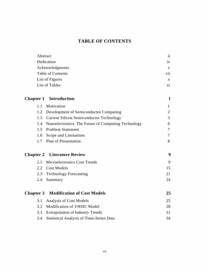
TABLE OF CONTENTS
Abstract iiDedication ivAcknowledgments vTable of Contents viiList of Figures xList of Tables xi
Chapter 1 Introduction 1
1.1 Motivation 11.2 Development of Semiconductor Computing 21.3 Current Silicon Semiconductor Technology 31.4 Nanoelectronics: The Future of Computing Technology 61.5 Problem Statement 71.6 Scope and Limitations 71.7 Plan of Presentation 8
Chapter 2 Literature Review 9
2.1 Microelectronics Cost Trends 92.2 Cost Models 152.3 Technology Forecasting 212.4 Summary 24
Chapter 3 Modification of Cost Models 25
3.1 Analysis of Cost Models 253.2 Modification of VHSIC Model 283.3 Extrapolation of Industry Trends 313.4 Statistical Analysis of Time-Series Data 34
viii
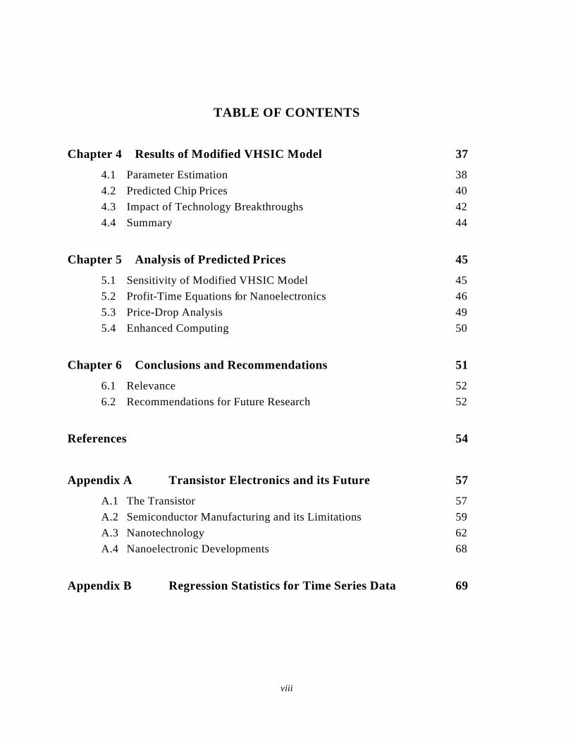
TABLE OF CONTENTS
Chapter 4 Results of Modified VHSIC Model 37
4.1 Parameter Estimation 384.2 Predicted Chip Prices 404.3 Impact of Technology Breakthroughs 424.4 Summary 44
Chapter 5 Analysis of Predicted Prices 45
5.1 Sensitivity of Modified VHSIC Model 455.2 Profit-Time Equations for Nanoelectronics 465.3 Price-Drop Analysis 495.4 Enhanced Computing 50
Chapter 6 Conclusions and Recommendations 51
6.1 Relevance 526.2 Recommendations for Future Research 52
References 54
Appendix A Transistor Electronics and its Future 57
A.1 The Transistor 57A.2 Semiconductor Manufacturing and its Limitations 59A.3 Nanotechnology 62A.4 Nanoelectronic Developments 68
Appendix B Regression Statistics for Time Series Data 69
ix
TABLE OF CONTENTS
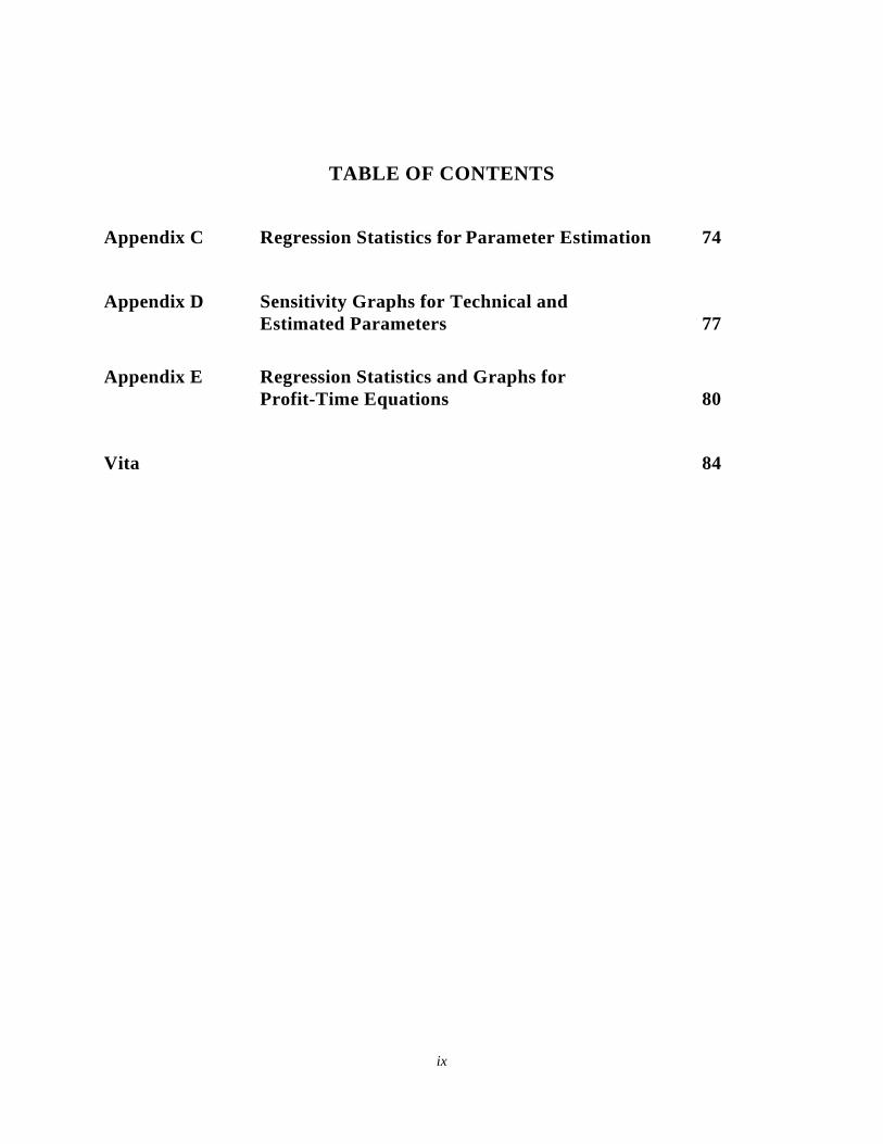
Appendix C Regression Statistics for Parameter Estimation 74
Appendix D Sensitivity Graphs for Technical andEstimated Parameters 77
Appendix E Regression Statistics and Graphs forProfit-Time Equations 80
Vita 84
x
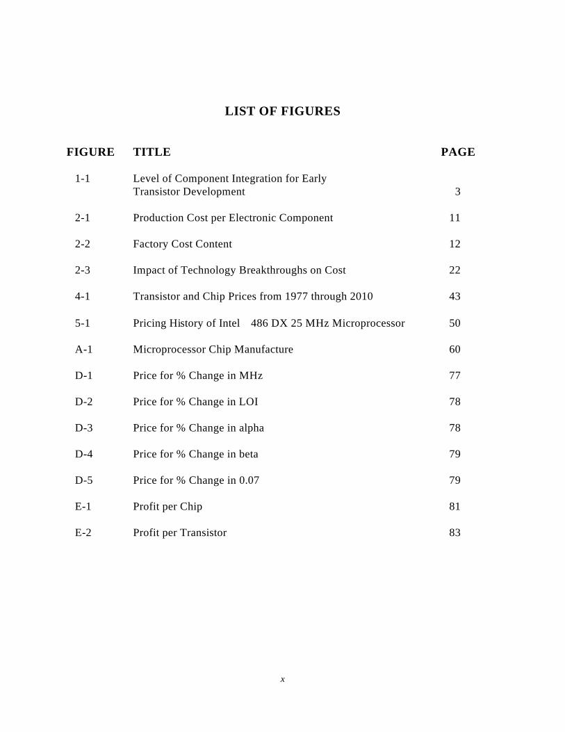
LIST OF FIGURES
FIGURE TITLE PAGE
1-1 Level of Component Integration for EarlyTransistor Development 3
2-1 Production Cost per Electronic Component 11
2-2 Factory Cost Content 12
2-3 Impact of Technology Breakthroughs on Cost 22
4-1 Transistor and Chip Prices from 1977 through 2010 43
5-1 Pricing History of Intel 486 DX 25 MHz Microprocessor 50
A-1 Microprocessor Chip Manufacture 60
D-1 Price for % Change in MHz 77
D-2 Price for % Change in LOI 78
D-3 Price for % Change in alpha 78
D-4 Price for % Change in beta 79
D-5 Price for % Change in 0.07 79
E-1 Profit per Chip 81
E-2 Profit per Transistor 83
11
LIST OF TABLES
TABLE TITLE PAGE
2-1 Initial Investment and Ownership Costs forPhotolithography Systems 13
2-2 Logic Transistor Cost from 1977 to 1992 20
3-1 High Performance On-Chip Clock Frequency 29
3-2 Prediction of Future Chip Cost Based on Trend Extrapolation 33
4-1 Historic Performance and Initial Prices of IntelSemiconductor Chips 39
4-2 Predicted Chip Price from Modified VHSIC Model 41
B-1 Regression of Transistor Cost Data 70
B-2 Regression of Transistor Content Data 71
C-1 Historical Intel Chips: Performance and Price 74
C-2 Data for the Calculation of the Durbin-Watson Statistic 75
E-1 MHz Data for Regression Analysis 80
E-2 Price per Transistor Data for Regression Analysis 82
Chapter 1: Introduction 1
CHAPTER 1
INTRODUCTION
1.1 Motivation
In today’s computing environment, the transistor is the fundamental element of the
microprocessor. As a device capable of processing much information quickly and efficiently,
microprocessors have proliferated because of the adoption of desktop computers all over the
world. The miniaturization of this fundamental component has proven to be among the most
important development toward processing more information more quickly. In order to
continue at the current rate of miniaturization, and to continue to increase the computing
capability of electronic computers, fundamental new technologies for nano-meter scale
electronics must be introduced. The subject of this report is an analysis of the economic
prospects of these new technologies for nanoelectronics. In order to make these economic
projections, it is first necessary to review some of the technical developments that provide the
background for the introduction of nanoelectronics [Monte95, Nanos95].
Computer users and researchers continue to demand more power and the ability to
process more complex information. To satisfy this demand in the next century, the
microelectronics industry must explore fundamental changes in the design and manufacture of
computing elements. This necessity has given birth to the field of nanoelectronics. Because
nanoelectronics deals with the construction of transistors and electronic devices on a scale
much smaller than current fabrication methods allow, new or modified manufacturing
processes must be developed. Several fabrication processes have been proposed. However,
the commercialization of such a process possibly lies up to 10 years in the future.
In this chapter, the ongoing efforts toward semiconductor device miniaturization will
be summarized. The photolithographic fabrication process and the physical limitations to
Chapter 1: Introduction 2
continued miniaturization will be described. The development of x-ray lithography and
electron-beam lithography as viable technologies for the future of electronics device
fabrication will be described. The impact that the experimental field of nanoelectronics may
have on the future of electronics computing will be highlighted. A more detailed description
of the technical concepts presented in this chapter is included in Appendix A. The problem
statement and the scope and limitations for this project will be stated. The plan of
presentation for this report will conclude the chapter.
1.2 Development of Semiconductor Computing
The “state-of-the-art” in the late 1940s before the advent of solid-state transistor
devices was the renowned ENIAC computer developed at the University of Pennsylvania.
ENIAC contained 19,000 vacuum tubes and was housed in a very large room that needed
constant cooling because of the large power consumption of the tubes [Noyce77].
Subsequently, vacuum tubes were replaced by solid-state devices based on the transistor.
This not only improved the reliability of electronic computers, but it also substantially
reduced the power required and associated heating problems. However, even more dramatic
improvements in computer performance appeared as a result of the miniaturization of such
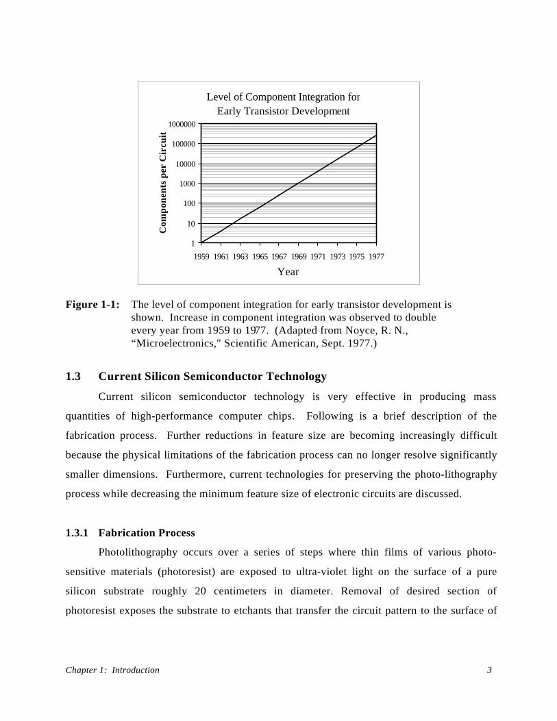
solid-state electronic devices over the next 45 years. The increase in the density of transistors
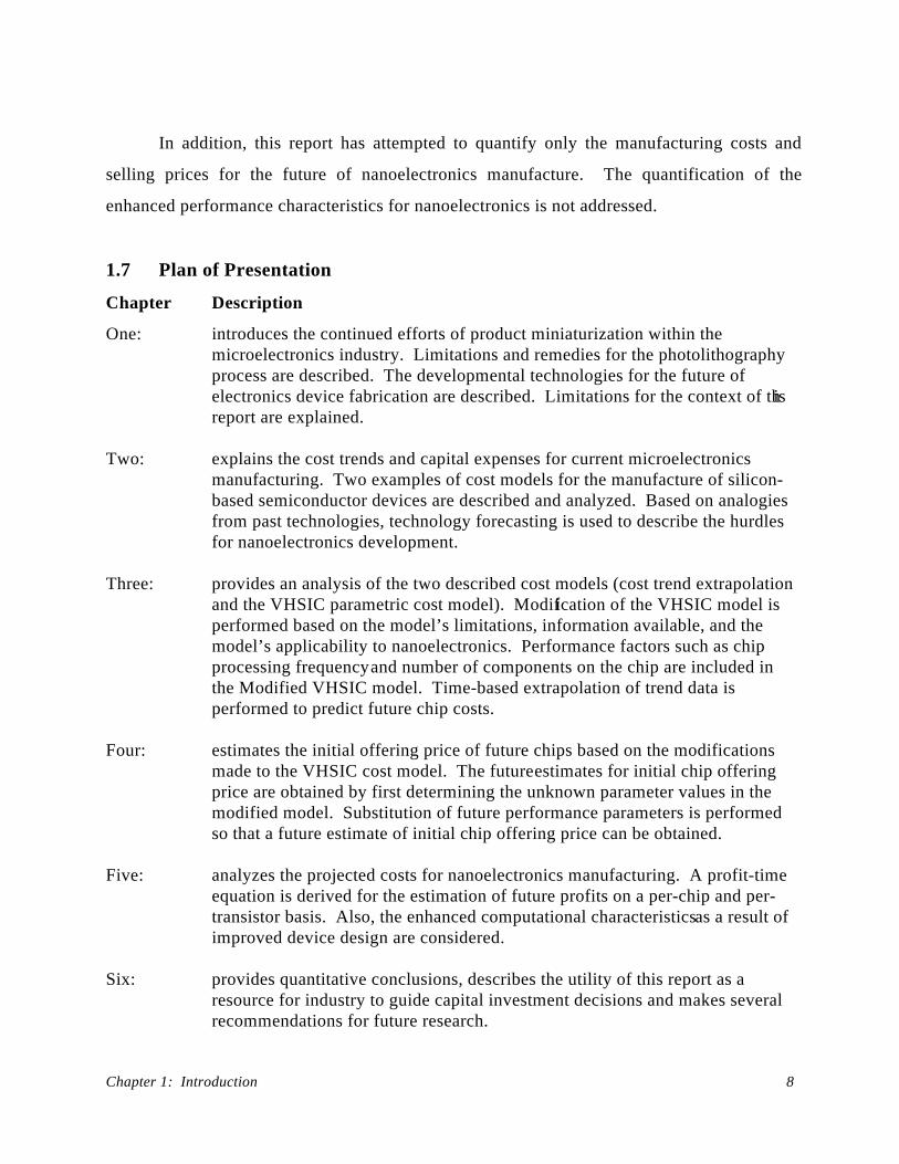
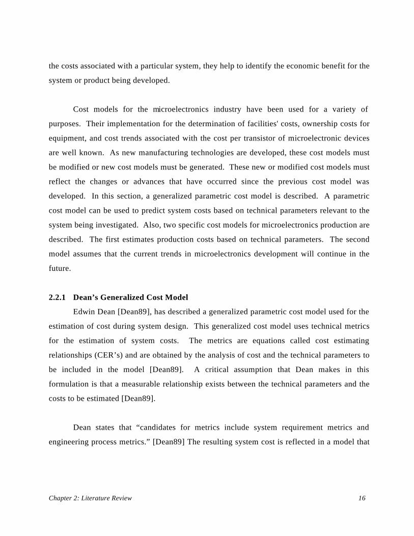
within electronic devices is plotted versus time for a portion of that period in Figure 1-1.
In the late 1970s the trend slowed to roughly a four-fold increase in transistor density
every three years. This trend, known as Moore’s Law [Hutch96] has been observed to
continue from 1977 through 1996.
Chapter 1: Introduction 3
Level of Component Integration for Early Transistor Development
1
10
100
1000
10000
100000
1000000
1959 1961 1963 1965 1967 1969 1971 1973 1975 1977
Year
Com
pone
nts
per
Cir
cuit
Figure 1-1: The level of component integration for early transistor development is shown. Increase in component integration was observed to double every year from 1959 to 1977. (Adapted from Noyce, R. N., “Microelectronics," Scientific American, Sept. 1977.)
1.3 Current Silicon Semiconductor Technology
Current silicon semiconductor technology is very effective in producing mass
quantities of high-performance computer chips. Following is a brief description of the
fabrication process. Further reductions in feature size are becoming increasingly difficult
because the physical limitations of the fabrication process can no longer resolve significantly
smaller dimensions. Furthermore, current technologies for preserving the photo-lithography
process while decreasing the minimum feature size of electronic circuits are discussed.
1.3.1 Fabrication Process
Photolithography occurs over a series of steps where thin films of various photo-
sensitive materials (photoresist) are exposed to ultra-violet light on the surface of a pure
silicon substrate roughly 20 centimeters in diameter. Removal of desired section of
photoresist exposes the substrate to etchants that transfer the circuit pattern to the surface of
Chapter 1: Introduction 4
the wafer. Doping of the wafer exposes the substrate to impurities such as boron or arsenic.
These impurities alter the electrical conductivity of circuit elements that are components of
the transistors that comprise the microprocessor [Stix95]. The finished wafer is then cut up
into individual chips that can number up to 200 for the 20 centimeter wafer [Hutch96].
A pictorial description of the chip fabrication process is shown in Appendix A of this report.
1.3.2 Physical Limitations
Transistors fabricated using photolithography have been remarkably easy to scale
down. As minimum feature sizes for transistors continue to decrease, their operational
characteristics will become affected. In addition, the manufacturing technology necessary to
obtain such small dimensions will become more complex, and obviously more expensive.
Current manufacturing technology has the capability to produce transistors with a
minimum feature size of 0.35 microns (350 nanometers) [SIA94]. The ability to continue to
produce devices with smaller feature sizes is dependent on various factors in the
manufacturing equipment and physical limitations of the transistor elements. Some of these
factors are listed below [Stix95].
1. Wavelength of Emitted Light2. Lens Focus on Photoresist3. Heat Dissipation4. Tunneling
A full description of these limitations is included in Appendix A of this report.
1.3.3 Lithography Solutions
With the limitations that are being slowly realized in the semiconductor industry,
manufacturers are attempting to circumvent those limitations while trying to maintain the
lithographic technologies of the past. Two of the more prominent proposals are the use of x-
Chapter 1: Introduction 5
ray lithography and electron beam lithography. A brief description for both of these
technologies as well as their advantages and disadvantages are presented below.
1.3.3.1 X-Ray Lithography
Fine resolution images have been achieved through the use of x-ray lithography. At
roughly one nanometer, the wavelength of x-rays are about three hundred times smaller than
the light used in today’s commercial systems. While conventional lithography systems can
use the radiation emitted from advanced lasers for production, x-ray lithography equipment
must use the radiation generated from a synchrotron as a source of radiation [Stix95]. A
synchrotron is an energy source that consists of two superconducting magnets whose electric
field confines electrons within a closed orbit. The electrons that circulate within the storage
ring emit x-rays that are used in the lithography process [Stix95].
Although synchrotrons are available in only a few of the most advanced universities,
IBM has developed the only commercial synchrotron storage ring in the United States
[Stix95]. IBM’s synchrotron system still remains a developmental project. A primary
technical obstacle to the commercial development of x-ray lithography is the lack of a feasible
way to focus x-rays. Also, x-ray lithography lacks the ability to demagnify the image. As a
result, the masks must outline the circuit image at the same small size as the image created on
the chip. The development of masks that can absorb the generated x-rays also poses a
problem. Since x-rays are high energy electromagnetic waves, masks must be made very
thick in relation to circuit features so that x-rays will not penetrate the mask [Stix95]. For
successful development of x-ray lithography the technical obstacles mentioned above must be
overcome.
1.3.3.2 Electron Beam Lithography
The use of electron beam lithography has a tremendous capability to produce high-
resolution features on silicon wafers. Resolution as small as tens of nanometers can be
Chapter 1: Introduction 6
achieved as a result of two factors: (1) electron beams have much shorter wavelengths than
current photolithographic light sources and (2) the electric fields that control the beams can be
focused very accurately [Gent94]. Electron beam lithography writes like a fine writing
instrument since the focus of the beam is computer-controlled. Slow production rates, in
comparison to conventional photolithographic techniques, make electron beam lithography
both time and cost inhibitive [Gent94].
1.4 Nanoelectronics: The Future of Computing Technology
The term nanotechnology has been used to describe a field of research that deals with
the manipulation of matter on an atomic scale. A nanometer, one-billionth of a meter (10-9
meters), is only about 10 atomic diameters. The fabrication of a computer based on nano-
scale components would realize a density of up to 10,000 times more than today’s most
advanced computers [Monte95].
The large microelectronics infrastructure currently in place will be an advantage for
the emergence of nano-scale computers based on electronic characteristics. Considering the
obstacles to continued miniaturization within semiconductor manufacturing technologies, the
operating principles that govern the devices within these “nanocomputers” must take
advantage of the limitations that are currently being experienced [Hans91]. Fabrication
techniques will eventually determine how small the devices can be built in practice.
The proposed nanoelectronics solutions to the obstacles of the microelectronics
industry come from diverse fields of interest. Researchers from the fields of biology,
chemistry, physics, and mechanics have proposed computational devices from their respective
fields [Monte95]. The true test of these systems will ultimately be whether their enhanced
performance characteristics will justify increased manufacturing costs when compared to
today’s most advanced computing systems.
Chapter 1: Introduction 7
Because smaller device sizes will allow semiconductor manufacturers to place a larger
number of logic gates within a chip, more computational power will be achieved. The
application of nanoelectronics manufacturing will also be applied to memory systems. The
development of nano-scale devices will not only provide the computer user with more power
and information storage capacity, but it may benefit society in the solution of previously
insoluble problems [Rola91]. For more information on the technologies, devices and
fabrication techniques for nanoelectronics see Appendix A for a detailed explanation.
1.5 Problem Statement
The problem under investigation is the estimation of selling prices and manufacturing
costs for nanoelectronics technology. Projections of current trends will indicate the future
manufacturing costs of semiconductor chips. Price estimates will be calculated by modifying
technical parameters of previous cost models for microelectronics. From these two
projections, the profit per chip and transistor can be obtained.
1.6 Scope and Limitations
Despite the comprehensive description of this research, there are several limitations.
This report estimates the future manufacturing costs of nanoelectronics technology based on
trend extrapolation and model modification. Because of the proprietary nature of the models
that some industry experts use, those models were not available to be included in this
research.
Only the silicon-based semiconductor electronics industry is examined in this report.
It is realized that the development of nano-computing may emerge within fields other than
electronics. Much effort has been expended to create nano-computing systems in quantum,
mechanical, and chemical fields. A more comprehensive description of these fields is
included in Appendix A of this report.
Chapter 1: Introduction 8
In addition, this report has attempted to quantify only the manufacturing costs and
selling prices for the future of nanoelectronics manufacture. The quantification of the
enhanced performance characteristics for nanoelectronics is not addressed.
1.7 Plan of Presentation
Chapter Description
One: introduces the continued efforts of product miniaturization within the microelectronics industry. Limitations and remedies for the photolithography process are described. The developmental technologies for the future of electronics device fabrication are described. Limitations for the context of this report are explained.
Two: explains the cost trends and capital expenses for current microelectronics manufacturing. Two examples of cost models for the manufacture of silicon-based semiconductor devices are described and analyzed. Based on analogies from past technologies, technology forecasting is used to describe the hurdles for nanoelectronics development.
Three: provides an analysis of the two described cost models (cost trend extrapolation and the VHSIC parametric cost model). Modification of the VHSIC model is performed based on the model’s limitations, information available, and the model’s applicability to nanoelectronics. Performance factors such as chip processing frequencyand number of components on the chip are included in the Modified VHSIC model. Time-based extrapolation of trend data is performed to predict future chip costs.
Four: estimates the initial offering price of future chips based on the modifications made to the VHSIC cost model. The future estimates for initial chip offering price are obtained by first determining the unknown parameter values in the modified model. Substitution of future performance parameters is performed so that a future estimate of initial chip offering price can be obtained.
Five: analyzes the projected costs for nanoelectronics manufacturing. A profit-time equation is derived for the estimation of future profits on a per-chip and per-transistor basis. Also, the enhanced computational characteristics as a result of improved device design are considered.
Six: provides quantitative conclusions, describes the utility of this report as a resource for industry to guide capital investment decisions and makes several recommendations for future research.
Chapter 2: Literature Review 9
CHAPTER 2
LITERATURE REVIEW
In this chapter, the cost trends for current microelectronics manufacturing will be
outlined. These cost trends will describe some of the unit production costs as well as the
facilities costs for the production of microelectronics circuits. The available cost data for the
development of x-ray lithography will also be included. A general form of a parametric cost
model will be given. Finally, cost trends and models for silicon-based semiconductor
manufacture will be described and analyzed.
Technology forecasting will be examined as a framework for the estimation of the
impact of innovative technologies. The impact of new manufacturing technologies for
electronics will be examined from analogies based on past technologies. By using this
approach, a prediction can be made for the future performance characteristics of electronics.
The limitations and cost factors for the previous technology will be discussed and analyzed
within the context of technology forecasting.
2.1 Microelectronics Cost Trends
One of the primary advantages for the development and production of
microelectronics circuits is the ability for those circuits to be manufactured in large batches at
low cost. Advances in manufacturing technology have allowed for the production of
microelectronics circuits with smaller features. These smaller features have allowed a greater
density of components to be placed on a chip and have reduced the cost per component within
these chips. The cost per component has decreased primarily because the technology for
placing more components on a chip has advanced more quickly than the capital costs for such
equipment. As manufacturers face technological limits for the processing of microelectronics
circuits, the ability to produce these circuits at such low unit costs may be weakened. This
Chapter 2: Literature Review 10
section of Chapter 2 will describe some of the cost considerations for the microelectronics
industry. Some of the unit cost trends will be discussed as well as the capital investments for
the facilities will be addressed.
2.1.1 Unit Cost Trends
The cost trends that will be addressed in this section primarily deal with the cost per
electronic function or cost per electronic component within a microelectronics circuit chip.
Such costs are usually computed by dividing the manufacturing cost per chip by the number
of components (transistors) within the chip. As shown in Figure 1-1, the number of
transistors on a chip has been shown to exponentially increase since the advent of solid-state
transistor electronics in the late 1950s. This exponential increase for the number of transistors
within a device has been met with an exponential decrease in the cost per transistor [Hess92].
This is not to say that the costs for the manufacturing technologies used to produce these
circuits has decreased. The capital investments for these technologies have increased,
however, technology advancements have allowed manufacturers to place more transistors on
a computer chip at a lower cost per transistor.
One example of the cost trends discussed in the previous paragraph is shown
pictorially in Figure 2-1. The production cost per electronic component for the production
year of a microelectronics chip is shown. The data for this figure was adapted from the 1994
National Technology Roadmap for Semiconductors. Although the Roadmap included
production costs for several areas of semiconductor manufacture (logic transistors and
memory transistors), the production costs shown are for the logic transistors used in
microprocessor chips [SIA94].
This figure clearly shows that there is an exponential relationship for the production
cost of transistors and the year in which the transistor was produced. As stated earlier, the
primary reason for this significant decrease in cost is that technology advances allow
Chapter 2: Literature Review 11
manufacturers to increase transistor density at a faster rate than the increases in capital
equipment costs. Only the production costs for solid-state production techniques are included
in this figure. No significant deviations for the unit cost trends were observed throughout the
years included in this figure.
Production Cost per Electronic Component
1
10
100
1000
1977 1980 1983 1986 1989 1992
Year
Cos
t (m
illic
ents
)
Figure 2-1: The production cost per electronic component in a microelectronicschip is shown. Production cost was observed to half every three years.
Adapted from SIA, “The National Technology Roadmap for Semiconductors,” 1994.)
2.1.2 Production Costs
Despite the lowered costs for the production of transistors on a unit basis, the actual
production costs per chip (and wafer) have been observed to increase with each generation of
processing equipment. These increases are described in the following section. The increasing
contribution of equipment for the Factory Cost Content is described. Factory Cost Content is
the contribution of resources (equipment, building, land, and improvement) to the total
production cost. Costs for the equipment similar to the ones used in today’s fabrication
facilities are listed in this section. As well, the estimated overall facilities costs are included
for some of the leading semiconductor manufacturers.
Chapter 2: Literature Review 12
2.1.2.1 Equipment and Factory Cost Content
As the equipment used in microelectronics factories becomes more complex and
expensive, the equipment’s contribution to the total cost of the factory is rising. With each
successive generation of equipment, the resolution for microelectronics chip production
becomes more precise. This resolution is largely dependent on the overlay of the processing
equipment. Overlay defines the precision with which an image can be placed on the chip
[SIA94]. Overlay is the determining factor in the complexity and accuracy for the
development of more advanced manufacturing equipment. As such, the cost for each
successive generation is affected by that complexity.
The contribution of the factory cost as a result of equipment expenditures can be seen
in Figure 2-2. This figure shows the percentage of Factory Cost Content from three
categories: Equipment, Improvements, and Building and Land. As shown in this figure, the
contribution that equipment has to the Factory Cost Content was observed to rise from 40% in
the Mid-1970s to approximately 70% in the Mid-1990s.
Factory Cost Content
55%
40%
70%
0%
20%
40%
60%
80%
Mid-70s Mid-80s Mid-90s
Fac
tory
Cos
t (%
)
EquipmentImprovementsBuilding and Land
Figure 2-2: The Factory Cost Content is shown for three categories: Equipment, Improvements, and Building and Land. In the past two decades, contributions from equipment have been observed to rise sharply[SIA94].
Chapter 2: Literature Review 13
2.1.2.2 Equipment Costs
Figure 2-2 shows that a critical cost component for semiconductor manufacturers is
equipment. The largest component of this cost is photolithography equipment (steppers).
Two important considerations for any long-term ownership are the initial cost of the stepper
and the long-term costs of ownership [Rub90]. The initial cost of the stepper sometimes
dictates the decision to purchase one stepper system over another. However, the costs of
ownership can often dictate the contribution that the stepper system will have to the overall
manufacturing cost of the product.
Several primary factors in the cost of ownership for photolithography equipment are
the annual depreciation, processing materials (resists and masks), the space required within a
cleanroom, and the spare parts requirements as a result of machine reliability. As stepper
systems become more advanced, both the initial investment cost and the cost of ownership
are expected to rise. Some of the initial investment and ownership costs are included for
several photolithography stepper systems in Table 2-1. The data for the following table were
taken from an article by Daniel Rubin, that appeared in Microelectronic Manufacturing and
Testing [Rub90].
Table 2-1: Initial Investment and Ownership Costs for Photolithography Systems
Lithography Equipment 1X 5X 5X Stepper
List Price $750,000 $1,500,00 $1,800,000Wafer Production/Year 19,106 18,876 23,348
Direct Labor/Wafer $17.99 $26.40 $26.40
Stepper Cost/Wafer $43.92 $71.30 $69.87
An important observation from the data given above is that although the initial
investment cost for the new 5X stepper is $300,000 higher than the traditional 5X stepper, the
new stepper has a higher throughput. This additional investment should be considered for
Chapter 2: Literature Review 14
those manufacturers who desire a high throughput of similar or identical products. The higher
throughput may justify the additional investment in the new stepper for some manufacturers.
Continued technological progress in photolithography has shifted the light used in the
fabrication process to lower and lower wavelengths. The photolithography equipment
described above exposes wafers in the visible portion of the electromagnetic spectrum
(approximately 380 nm). Low wavelength ultra-violet light (still in the visible portion of the
spectrum) is still being used to expose wafers. Preliminary research for the use of x-rays to
expose wafers has been undertaken by IBM. X-Ray sources emit electromagnetic waves that
are not in the visible portion of the electromagnetic spectrum (approximately 10 to 30 nm).
Many researchers feel that the research for x-ray lithography techniques was performed much
too early [Stix95]. However, processing limitations in the visible portion of the spectrum are
becoming more evident with each new generation of conventional lithography equipment.
Following is a description of the costs incurred by IBM from their preliminary research of x-
ray lithography.
According to Stix [Stix95], IBM has performed initial research for the use of x-rays as
an exposure source for the processing of silicon wafers. This research primarily consisted of
designing a synchrotron to produce x-rays that could supply multiple steppers with the ‘light’
to expose the wafers [Stix95]. The price tag for the development of a synchrotron was
estimated at $20 to $50 million. An advantage for such a system is that a single synchrotron
could supply up to 16 steppers simultaneously. At present, each stepper has an independent
exposure source. Other technical obstacles that prevent IBM from fully developing this x-ray
system include: focusing the x-rays, reduction of the image, fabrication of the masks and
development of resists. In total, IBM spent several hundred million dollars on the research
[Stix95]. Stix mentions that in late 1995 an alliance within the semiconductor industry would
decide whether such a system should be prepared for production. Information regarding any
decision from the alliance has not been identified.
Chapter 2: Literature Review 15
2.1.2.3 Facilities Costs
Another key piece of evidence that the technological and economic limits to
semiconductor manufacture are close is the sharp rise in facility costs. The primary cost
driver for the sharp rise in facility costs is the clean rooms within which processing of the
silicon wafers occurs. Processing rooms must be nearly particle-free. The clean room
requirements for such facilities drive initial costs to over five thousand dollars ($5,000) per
square foot [Cast94]. This price only includes the construction cost, the specialty equipment
cost, and hookup costs for the equipment. Excluded from this estimate are the costs for the
actual processing equipment used in the wafer fabrication processes [Cast94].
Despite these large costs, semiconductor manufacturers continue to heavily invest in
the construction of these facilities. Intel is spending $1.1 billion for a factory in Oregon and
$1.3 billion for a facility in Chandler, Arizona. Samsung and Siemens are building plants that
are each estimated to cost $1.5 billion. Motorola, IBM, and Toshiba also have plans for the
construction of facilities costing over one billion dollars each [Hutch96]. A direct
consequence of the rise in facility costs is the formation of alliances between the
semiconductor manufacturers to share technological advances and development costs. Such
alliances will be instrumental in the development of a commercial x-ray lithography system.
2.2 Cost Models
For a system that has yet to be developed, the generation and analysis of a cost model
is not only desired, but necessary to justify the development costs for production. As new
manufacturing processes for microelectronics are developed, the economic success of such
systems are determined by their cost effectiveness and the benefit generated for a particular
cost. The economic benefit is directly measured by the market selling price of the products
developed by the particular system. Systems whose economic benefit exceeds the costs
generated by that system are economically desired provided that the margin of excess benefit
exceeds an expected hurdle or percentage rate. Accurate cost models not only help to predict
Chapter 2: Literature Review 16
the costs associated with a particular system, they help to identify the economic benefit for the
system or product being developed.
Cost models for the microelectronics industry have been used for a variety of
purposes. Their implementation for the determination of facilities' costs, ownership costs for
equipment, and cost trends associated with the cost per transistor of microelectronic devices
are well known. As new manufacturing technologies are developed, these cost models must
be modified or new cost models must be generated. These new or modified cost models must
reflect the changes or advances that have occurred since the previous cost model was
developed. In this section, a generalized parametric cost model is described. A parametric
cost model can be used to predict system costs based on technical parameters relevant to the
system being investigated. Also, two specific cost models for microelectronics production are
described. The first estimates production costs based on technical parameters. The second
model assumes that the current trends in microelectronics development will continue in the
future.
2.2.1 Dean’s Generalized Cost Model
Edwin Dean [Dean89], has described a generalized parametric cost model used for the
estimation of cost during system design. This generalized cost model uses technical metrics
for the estimation of system costs. The metrics are equations called cost estimating
relationships (CER’s) and are obtained by the analysis of cost and the technical parameters to
be included in the model [Dean89]. A critical assumption that Dean makes in this
formulation is that a measurable relationship exists between the technical parameters and the
costs to be estimated [Dean89].
Dean states that “candidates for metrics include system requirement metrics and
engineering process metrics.” [Dean89] The resulting system cost is reflected in a model that
Chapter 2: Literature Review 17
provides a mathematical relationship to the system cost being estimated. Dean’s Generalized
Cost Model is stated below:
c e e xa a xja
j r
s
i
ro i i j=
= +=∏∏
11
Dean states that the exponential factors of the model are useful for normalizing cost of
temporal effects of technology escalation and binary categories [Dean89]. The power law
factors are useful for normalizing cost for economic quantities of production units. This
generalized model is advantageous over simple models because the “combination of these
factors usually improves accuracy over the use of either separately.” [Dean89]
2.2.2 Advanced Technology Models for VHSIC
Efforts to determine costs for Air Force Avionics have produced a cost model that
estimates the costs for the implementation of VHSIC (Very High-Speed Integrated Circuits)
in avionics systems. VHSIC was initiated by the Defense Department to skip an entire
generation of microelectronic technology and move military electronics into the era of
commercial and consumer electronics [Hess92]. This analysis is presented in a report
entitled: “Estimating the Cost of Advanced Technology,” by the RAND Corporation. In the
report, the cost implications of VHSIC are discussed. Also, an approach to performing cost
estimates for such systems is presented. Although the cost estimates performed by RAND do
not directly deal with cost estimation for the fabrication of microelectronics circuits, the
methods applied for estimation of cost are of primary interest.
The VHSIC Cost Estimation Model specifically addresses the costs for the
development of avionics computer systems. The VHSIC Model is similar to the generalized
model described in Dean’s report. This similarity shows that the RAND Corporation used an
standard and accepted format for the development of their cost model. The challenge for the
Chapter 2: Literature Review 18
development of these estimates is that the development of such a system is unlike any systems
that appeared in historical cost databases. The significance of making such cost estimates was
that the electronics within avionics systems was found to contribute up to 50% of the total
cost of the aircraft [Hess92]. Therefore, accurate cost estimates were desired early in the
design/manufacturing process.
A technology forecasting approach was used to estimate costs in the VHSIC model.
The cost trends described earlier in Figures 1-1 and 2-1 were used to approximate a
relationship between the level of integration on the circuit chip and the cost per component on
the chip. The authors asserted that if such a relationship could be projected, it could be used
to help forecast the cost of future systems [Hess92]. For the specific application developed by
the RAND Corporation, the researchers chose to select specific cost drivers that reflect the
established cost trends for microelectronics development. After considering a number of
candidates to be included in the theoretical cost model, three cost drivers were selected.
These three drivers are the number of gates on the chip, the weight for the system, and a
binary variable to reflect the maturity of the technology being utilized [Hess92]. This binary
variable was chosen to reflect the utilization of a product before or after two years from its
initial availability. If the technology was implemented during the first two years of its
availability, the variable is given a value of 1, otherwise the value is 0.
The researchers at the RAND Corporation expected the relationships between the
parameters specified within the model and the system cost to be non-linear. As such, the
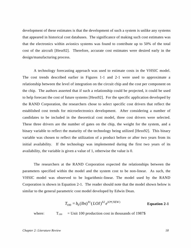
VHSIC model was observed to be logarithmic-linear. The model used by the RAND
Corporation is shown in Equation 2-1. The reader should note that the model shown below is
similar to the general parametric cost model developed by Edwin Dean.
T b lbs LOI eb b b NEW100 0
1 2 3= ( ) ( ) *( ) Equation 2-1
where: T100 = Unit 100 production cost in thousands of 1987$
Chapter 2: Literature Review 19
LBS = System weight (in pounds)
LOI = Level of integration (number of transistors/chip)
NEW = 0 mature technology, 1 new technology
bi = numerical constants (no units)
Since RAND expected costs to increase at a decreasing rate with weight and level of
integration, the values of b1 and b2 were specified to be less than one.
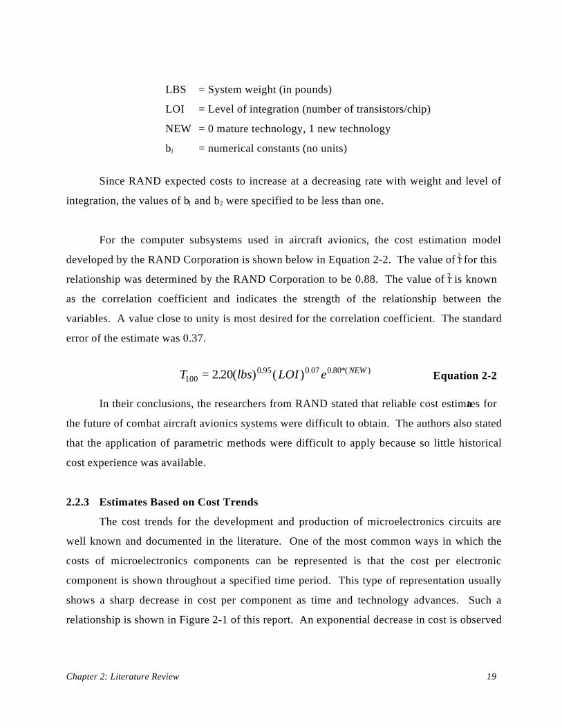
For the computer subsystems used in aircraft avionics, the cost estimation model
developed by the RAND Corporation is shown below in Equation 2-2. The value of r2 for this
relationship was determined by the RAND Corporation to be 0.88. The value of r2 is known
as the correlation coefficient and indicates the strength of the relationship between the
variables. A value close to unity is most desired for the correlation coefficient. The standard
error of the estimate was 0.37.
T lbs LOI e NEW100
0 95 0 07 0 802 20= . ( ) ( ). . . *( ) Equation 2-2
In their conclusions, the researchers from RAND stated that reliable cost estimates for
the future of combat aircraft avionics systems were difficult to obtain. The authors also stated
that the application of parametric methods were difficult to apply because so little historical
cost experience was available.
2.2.3 Estimates Based on Cost Trends
The cost trends for the development and production of microelectronics circuits are
well known and documented in the literature. One of the most common ways in which the
costs of microelectronics components can be represented is that the cost per electronic
component is shown throughout a specified time period. This type of representation usually
shows a sharp decrease in cost per component as time and technology advances. Such a
relationship is shown in Figure 2-1 of this report. An exponential decrease in cost is observed
Chapter 2: Literature Review 20
primarily because technology advances have been implemented faster than increases in
processing costs.
The cost trends represented can exist for any component of the microelectronics
fabrication. In Figure 2-1, the trends are represented for logic transistors fabricated for
microprocessors. These microprocessors are typically used in desktop computer applications.
The trends developed in Figure 2-1 were adapted from data given by the Semiconductor
Industry Association (SIA). This data showed the historical relationship between the cost per
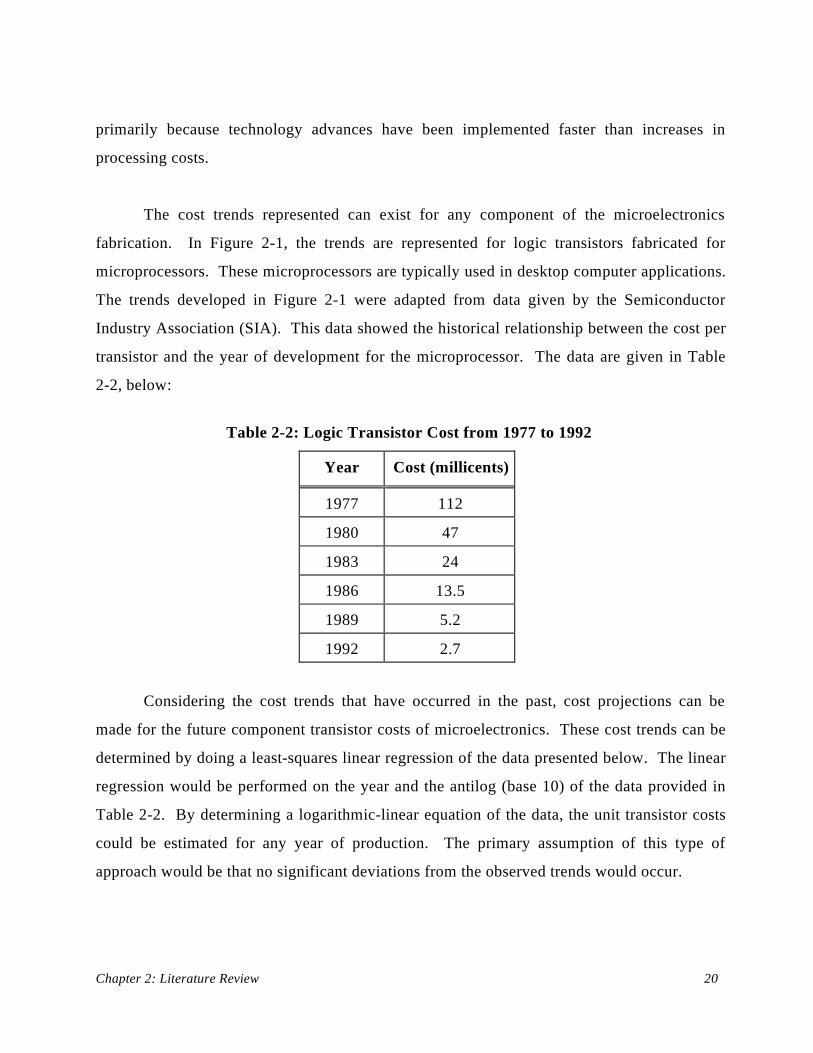
transistor and the year of development for the microprocessor. The data are given in Table
2-2, below:
Table 2-2: Logic Transistor Cost from 1977 to 1992
Year Cost (millicents)
1977 112
1980 47
1983 24
1986 13.5
1989 5.2
1992 2.7
Considering the cost trends that have occurred in the past, cost projections can be
made for the future component transistor costs of microelectronics. These cost trends can be
determined by doing a least-squares linear regression of the data presented below. The linear
regression would be performed on the year and the antilog (base 10) of the data provided in
Table 2-2. By determining a logarithmic-linear equation of the data, the unit transistor costs
could be estimated for any year of production. The primary assumption of this type of
approach would be that no significant deviations from the observed trends would occur.
Chapter 2: Literature Review 21
2.3 Technology Forecasting
Technology forecasting describes a field that is interested in the logical analysis of
systems that leads to a performance objective or hurdles for the development and
implementation of a particular technology. Such conclusions assist and identify the economic
potentials and impact of technological progress [Lan69]. This field differs from opinion-
based conclusions in that technological forecasts rest upon an explicit set of quantitative
relationships and assumptions [Brig68]. Three primary groups that are interested in the
outcome of these forecasts are business economists, managers of corporate technology, and
government agencies such as the military. Such organizations may use these forecasts to
predict future business trends, to decide future product strategy, or to determine future
systems capabilities [Brig68].
A common approach for the implementation of technological forecasts is the
observation of performance or cost trends within the industry of interest. By identifying the
trends that characterize the industry, extrapolation of those trends can predict the future
performance characteristics for the parameter of interest. The use of technology forecasting
through the use of trend extrapolation avoids the problem of making detailed predictions
about the development of specific devices. A disadvantage, however, is that trend
extrapolation merely states that a certain level will be achieved. It does not indicate whether
existing devices can be improved or whether a new device will be invented [Mart72]. By
using several parameters to identify the advancement of the industry, the performance or cost
of a future system can be predicted. Such a method is called parametric cost estimating based
on technological forecasting.
As technological forecasting can predict the enhanced performance of a new or
revolutionary technology, some attention must be given to the effects of technology
breakthroughs. Figure 2-3 shows the effect of technological progress on the manufacturing
cost of a product. The technological barriers T1 and T2 are where improvements in product
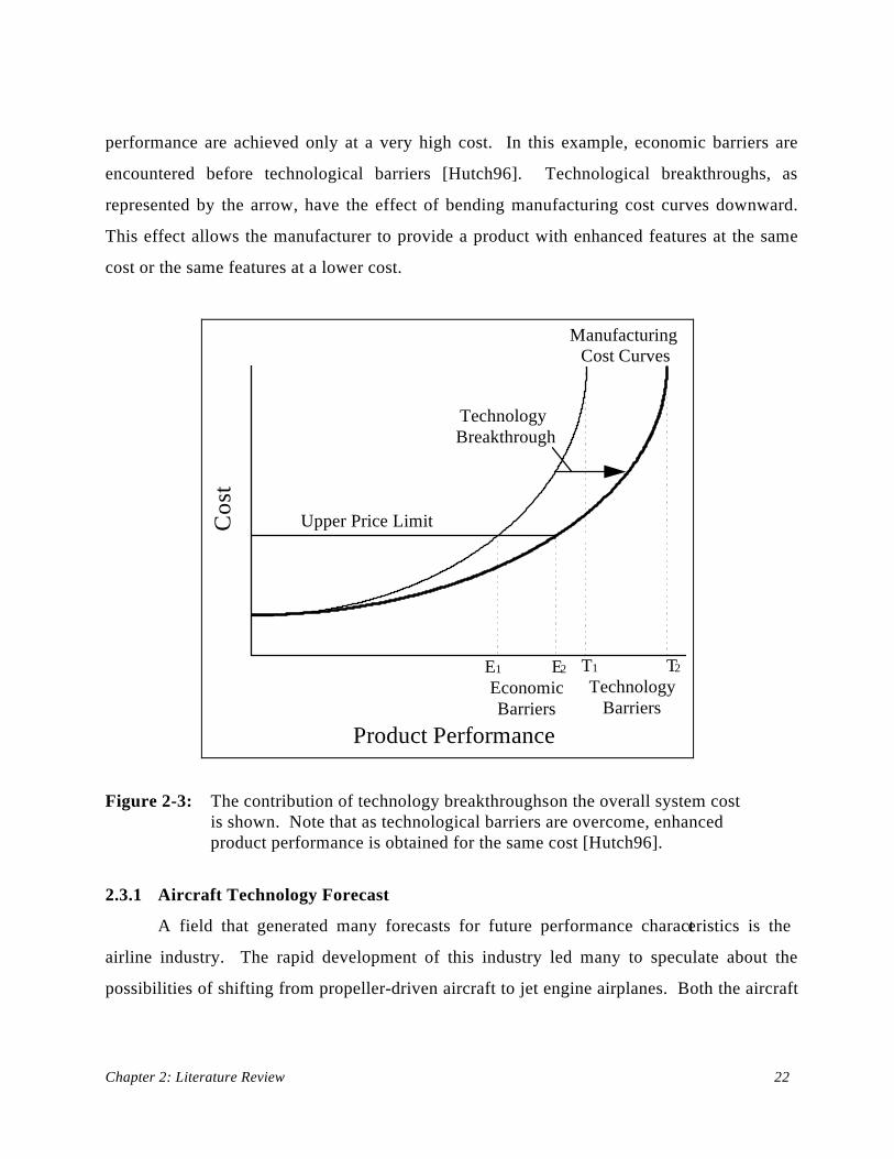
Chapter 2: Literature Review 22
performance are achieved only at a very high cost. In this example, economic barriers are
encountered before technological barriers [Hutch96]. Technological breakthroughs, as
represented by the arrow, have the effect of bending manufacturing cost curves downward.
This effect allows the manufacturer to provide a product with enhanced features at the same
cost or the same features at a lower cost.
Manufacturing Cost Curves
Technology Breakthrough
Cos
t
Product Performance
Upper Price Limit
E1 E2
EconomicBarriers
T1 T2
TechnologyBarriers
Figure 2-3: The contribution of technology breakthroughs on the overall system cost is shown. Note that as technological barriers are overcome, enhanced product performance is obtained for the same cost [Hutch96].
2.3.1 Aircraft Technology Forecast
A field that generated many forecasts for future performance characteristics is the
airline industry. The rapid development of this industry led many to speculate about the
possibilities of shifting from propeller-driven aircraft to jet engine airplanes. Both the aircraft
Chapter 2: Literature Review 23
and semiconductor industries were originally driven by military demand for their product
[Hutch96]. For aviation, the shift from military application to a consumer product was driven
by the reduction in cost per mile traveled, while also reducing the flight time. For
semiconductor electronics, consumers have benefited from the efforts of industry to increase
component densities (also increasing performance), while lowering chip costs [Hutch96].
A primary indicator of performance in the aviation industry is maximum speed. As
aviation development grew, the speculation for advanced performance led some industry
experts to predict supersonic travel. These predictions were later verified with the invention
of the Concorde. This invention, and its application for supersonic trans-oceanic travel, is still
a subject of much debate. Although the increase in speed was a natural extension of past
trends, Concorde travel is still not economically feasible for most travelers. A major pitfall
for the adoption of widespread use of Concorde travel was the noise pollution generated from
the sonic boom of deceleration [Hutch96]. Despite the limitations for advancement, the
airline industry did not falter. Instead, a greater diversity of smaller aircraft were designed
and built for more specific markets [Hutch96]. The focus of development shifted from size
and speed to efficiency, quality, and comfort [Hutch96].
2.3.2 Hurdles for Nanoelectronics
Similar to the development of the Concorde, nanoelectronics is expected to be a
natural extension of an observed trend. That trend, the level of integration for components on
a microprocessor chip, has been observed to increase exponentially for the past three decades.
Although the obstacles for continued development appear insurmountable, semiconductor
industry researchers have previously overcome similar obstacles [Stix95]. The continued
demand for semiconductor electronics will fuel the research for more innovative solutions for
the ongoing miniaturization of the transistor.
Chapter 2: Literature Review 24
Among the obstacles that must be overcome, the most prominent is the search for a
lithography system that can resolve smaller images [Stix95]. For much smaller wavelengths,
the application of x-ray lithography appears to be an alternative with several major hurdles for
full commercial development [Stix95]. Also necessary is a circuit design that will take
advantage of the quantum effects experienced for such small circuit features [Bate88]. The
immediate solution to these obstacles is not clear. However, technology forecasting can be
used as a tool to determine the future performance level of semiconductor devices.
2.4 Summary
This chapter has described some preliminary considerations for cost trends associated
with the continued development of the semiconductor industry. One of the primary
advantages for the continued decrease in semiconductor costs is that technological
advancements have outpaced the increased cost of manufacturing computer chips. However,
increases in the total cost of processing equipment have been observed to rise over the past
two decades. As manufacturers seek to develop more advanced manufacturing hardware, the
facilities costs have also risen. Facilities currently under construction may cost in excess of
one billion dollars. The primary contribution for the large cost of these facilities is the
equipment for processing and the preparation of the clean-room environments.
Two methods for the estimation of future costs have also been discussed in Chapter 2.
These costing methods use industry trends to extrapolate a future industry parameter. As
observed from the generation of the VHSIC Cost Model, the application of technology
forecasting is possible for the prediction of future performance parameters. These parameters
can then be used in a cost model to estimate the future manufacturing costs of an industry. A
similar study is to be performed for the commercialization of x-ray lithography manufacturing
systems.
Chapter 3: Modification of Cost Models 25
CHAPTER 3
MODIFICATION OF COST MODELS
The VHSIC Model and the cost trends described in the previous chapter were shown
to address some of the past and current production costs for microelectronics. Although the
models discussed may accurately describe the manufacturing costs for past or current
microelectronics systems, their application to future systems is limited. The primary purpose
of this report is to estimate the future manufacturing costs of nanoelectronics. Therefore, the
cost models previously identified must be modified to reflect the future properties or
performance characteristics of nanoelectronics.
In this chapter, the advantages, disadvantages and complexity of the previously
described cost models are addressed. Considering the technology forecasting analogy,
predictions for future performance factors will be made for nanoelectronics. These
predictions will be extrapolations of currently observed industry trends. It is realized that the
cost models analyzed may not reflect future manufacturing costs based on the specified
performance characteristics or the available data. In that case, the models will be modified to
reflect the performance characteristics or manufacturing technology of the next generation of
electronics. Such performance characteristics include, but are not limited to number of
components on the chip, product yield, minimum feature size of the devices on the chip, and
processing frequency of the integrated circuit chip.
3.1 Analysis of Cost Models
The primary advantage for the development of a cost model is to obtain a macroscopic
view of costs by using several measurable parameters. These parameters should exist within
the system or process that is being examined. The two models discussed in Chapter 2 are a
Chapter 3: Modification of Cost Models 26
parameter-based model for the estimation of microelectronics costs and a cost trend model for
the estimation of per transistor costs. In this section of Chapter 3, the advantages,
disadvantages, and complexity of each of these models is discussed. The relevance and
applicability of these models is also addressed. The generic model specified by Dean will be
used as a basis for the development of a parametric-price model for nanoelectronics. Portions
of the VHSIC model will be used to generate a Modified VHSIC Model. Later, chip costs
will be estimated by extrapolating chip transistor content and transistor costs.
3.1.1 VHSIC Model
The VHSIC Model developed by the RAND Corporation for cost estimation of
avionics computer systems is identical in form to the general model specified by Dean.
Although future nanoelectronics technology will not be identical to the computer system
technology examined by RAND, some modifications of the VHSIC Model can be performed
to suit the purposes of this report. Following is a brief analysis of the VHSIC model. Later,
adjustments to this model will be made based on this analysis and the technology forecasting
analogy described in Section 2.3 of this report.
The VHSIC model predicts costs based on perceived relationships of technical
parameters to costs. Such a model is typically referred to as a parametric-cost model. A
primary advantage of parametric-cost models is that the relationship of technical parameters
to the cost is easy to understand. Such models have been used frequently for the evaluation of
system costs early in the development of the product life cycle. Some difficulties arise in the
number of technical parameters that can be used in parametric cost estimating. Often, model
complexity prohibits all possible parameters from being included. Also, accuracy of the cost
model depends on the parameters and the data that are available.
The application of the VHSIC model for the estimation of avionics system costs was
made relevant because of the data available for the statistical analysis of the model. The
Chapter 3: Modification of Cost Models 27
investigators from RAND found that the model developed for avionics computer systems had
an r2 value of 0.88 and a standard error of 0.37. The availability of current data will also play
a significant role for the cost estimation of future semiconductor manufacturing. The quantity
of data available for the present research does not match up well to the data available to the
RAND Corporation. A modified version of a statistically significant model is to be used in
this project. By using such a model, it is believed that reliable estimates can be achieved for
the future selling price of semiconductor chips.
3.1.2 Cost Trends
Analysis of the business cycle for any industry is likely to produce some type of trend
in the cost or demand of the product. In the semiconductor industry, an interesting trend is
the exponential decrease in transistor cost. As shown in Figure 2-1, the present cost per
transistor on a microprocessor chip has fallen to a couple of millicents. In this analysis, we
assume that no major cost trend shifts will occur. For such clearly defined trends, the
assumption of continuation for the trend is usually valid. An additional advantage for the use
of cost trends is that the extrapolation of consistent, well-defined trends is easy to perform.
A limited view of the manufacturing cost is sometimes obtained, however, when only
one parameter is used to predict manufacturing cost. Without other data, the increasing
contribution of equipment for the total cost of the factory would not have been known. The
inclusion of as many factors as possible is usually desired for more accurate cost estimates.
However, model complexity often limits the number of parameters that can be estimated
reasonably well. For a more complete picture of industry costs, cost trend data should be
used in conjunction with other semiconductor industry parameters such as manufacturing
complexity and product performance.
Chapter 3: Modification of Cost Models 28
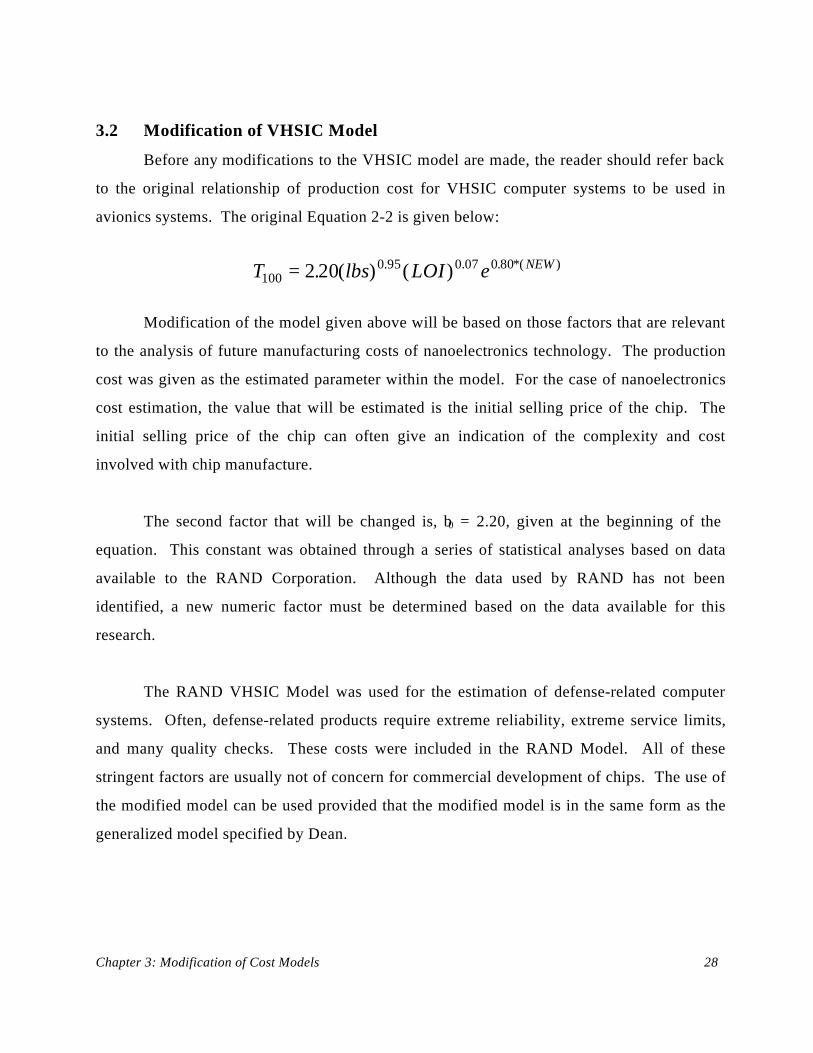
3.2 Modification of VHSIC Model
Before any modifications to the VHSIC model are made, the reader should refer back
to the original relationship of production cost for VHSIC computer systems to be used in
avionics systems. The original Equation 2-2 is given below:
T lbs LOI e NEW100
0 95 0 07 0 802 20= . ( ) ( ). . . *( )
Modification of the model given above will be based on those factors that are relevant
to the analysis of future manufacturing costs of nanoelectronics technology. The production
cost was given as the estimated parameter within the model. For the case of nanoelectronics
cost estimation, the value that will be estimated is the initial selling price of the chip. The
initial selling price of the chip can often give an indication of the complexity and cost
involved with chip manufacture.
The second factor that will be changed is, b0 = 2.20, given at the beginning of the
equation. This constant was obtained through a series of statistical analyses based on data
available to the RAND Corporation. Although the data used by RAND has not been
identified, a new numeric factor must be determined based on the data available for this
research.
The RAND VHSIC Model was used for the estimation of defense-related computer
systems. Often, defense-related products require extreme reliability, extreme service limits,
and many quality checks. These costs were included in the RAND Model. All of these
stringent factors are usually not of concern for commercial development of chips. The use of
the modified model can be used provided that the modified model is in the same form as the
generalized model specified by Dean.
Chapter 3: Modification of Cost Models 29
A significant consideration in the development of any system used in an aircraft is the
weight contribution for that system. The researchers at RAND recognized this important
factor and included it in the model that they developed. For the development of future
computing processors used in conventional computer systems, weight is not a significant
consideration. As such, its inclusion in the model to estimate future manufacturing prices of
nanoelectronics technology is not appropriate. Because the exponent for the weight factor
was based solely on the contribution of weight to aircraft subsystem costs, its inclusion in the
modified cost model is also not appropriate.
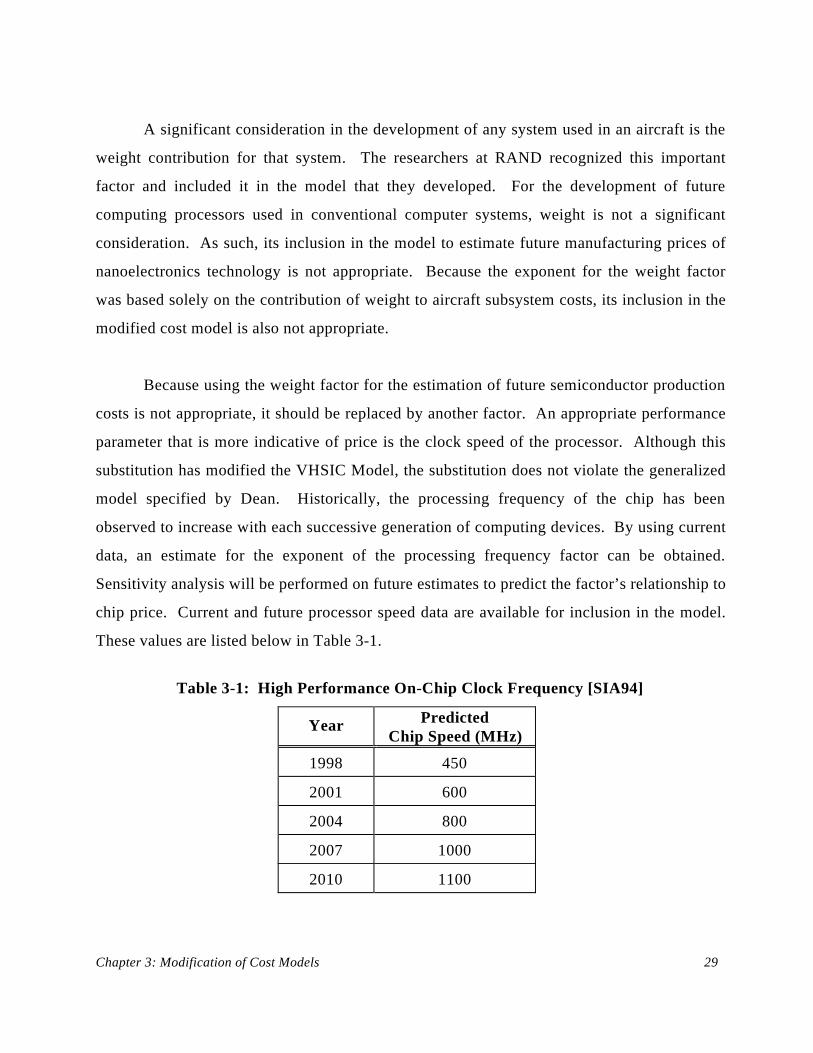
Because using the weight factor for the estimation of future semiconductor production
costs is not appropriate, it should be replaced by another factor. An appropriate performance
parameter that is more indicative of price is the clock speed of the processor. Although this
substitution has modified the VHSIC Model, the substitution does not violate the generalized
model specified by Dean. Historically, the processing frequency of the chip has been
observed to increase with each successive generation of computing devices. By using current
data, an estimate for the exponent of the processing frequency factor can be obtained.
Sensitivity analysis will be performed on future estimates to predict the factor’s relationship to
chip price. Current and future processor speed data are available for inclusion in the model.
These values are listed below in Table 3-1.
Table 3-1: High Performance On-Chip Clock Frequency [SIA94]
Year PredictedChip Speed (MHz)
1998 450
2001 600
2004 800
2007 1000
2010 1100
Chapter 3: Modification of Cost Models 30
A significant factor in the model developed by RAND was the level of integration
factor (LOI). This factor was used to predict system costs based on the number of transistors
used on a chip. For the purpose of this research, the inclusion of the LOI factor is desired and
its inclusion in the modified model is appropriate. As the exponent for the LOI factor has
been determined from multiple analyses of computer system costs, the exponent will remain
unchanged in the modified model. A critical assumption made in this project is that the LOI
factor will affect commercial system prices in the same way as defense system costs.
Sensitivity analysis will be performed on future estimates to predict the exponent’s
relationship to chip price.
The last factor of the model, e NEW0 80. *( ) was used as a parameter to increase the
estimated cost depending on the date of technology implementation. The estimated cost
would increase by a factor of e0 80. , or 2.23, if the technology within the avionics system was
implemented within two years of its first commercial introduction. Otherwise, the estimated
cost would only depend on the previous factors included in the model. This binary factor
merely provides a constant multiplier for the estimation of the avionics computer system costs
examined by RAND. The first factor in the modified model is also a constant. In the
modified model, the first factor will compensate for the binary factor given as the last
parameter of the original model.
Some critical assumptions have been made for the modification of the VHSIC cost
model. First, it is assumed that the replacement of the weight parameter by a clock speed
factor does not significantly affect the integrity of the cost estimating relationship. Also, it is
assumed that the exponential parameter of the LOI term reflects semiconductor technology
advances and not aircraft avionics advances. The constant exponent for the LOI factor is also
assumed to remain unaffected by significant technological changes in semiconductor
technology. Reusing the exponent for the LOI factor also assumes that commercial system
prices will be affected in the same manner as defense-related costs. Finally, it is assumed that
Chapter 3: Modification of Cost Models 31
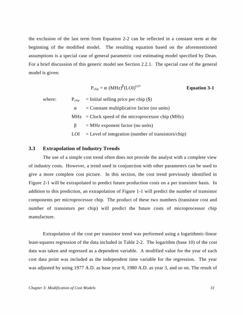
the exclusion of the last term from Equation 2-2 can be reflected in a constant term at the
beginning of the modified model. The resulting equation based on the aforementioned
assumptions is a special case of general parametric cost estimating model specified by Dean.
For a brief discussion of this generic model see Section 2.2.1. The special case of the general
model is given:
Pchip = α (MHz)β(LOI)0.07 Equation 3-1
where: Pchip = Initial selling price per chip ($)
α = Constant multiplicative factor (no units)
MHz = Clock speed of the microprocessor chip (MHz)
β = MHz exponent factor (no units)
LOI = Level of integration (number of transistors/chip)
3.3 Extrapolation of Industry Trends
The use of a simple cost trend often does not provide the analyst with a complete view
of industry costs. However, a trend used in conjunction with other parameters can be used to
give a more complete cost picture. In this section, the cost trend previously identified in
Figure 2-1 will be extrapolated to predict future production costs on a per transistor basis. In
addition to this prediction, an extrapolation of Figure 1-1 will predict the number of transistor
components per microprocessor chip. The product of these two numbers (transistor cost and
number of transistors per chip) will predict the future costs of microprocessor chip
manufacture.
Extrapolation of the cost per transistor trend was performed using a logarithmic-linear
least-squares regression of the data included in Table 2-2. The logarithm (base 10) of the cost
data was taken and regressed as a dependent variable. A modified value for the year of each
cost data point was included as the independent time variable for the regression. The year
was adjusted by using 1977 A.D. as base year 0, 1980 A.D. as year 3, and so on. The result of
Chapter 3: Modification of Cost Models 32
this regression provides the cost per transistor for any modified year value. This expression is
given by Equation 3-2. The predicted future costs per transistor (Ctrans) are given in Table 3-2,
below. Regression output for this data is included in Appendix B of this report.
log ( ) . . * (mod )10 2 0304 01067C yeartrans = − Equation 3-2
The expression above is remarkably similar to a regression equation based on the
Chow Price Index. This index consists of three measures of computing power (multiplication
time, memory size, and access time) [Bro75]. The price index used 1960 as a base year and
computes the 1960 rental value computing power in thousands of dollars [Bro75]. All
estimates made by the Chow Price Index assume that the rate of price change over time
represents the rate of technological progress [Bro75]. The regression of the Chow Price Index
on time for the years 1956 to 1965 is shown below:
log . . *10 154 0 237price time= − r2 = 0.99 Equation 3-3
A logarithmic least-squares regression was also performed for the number of transistor
components on a computing chip. The data for this regression was taken from historical
transistor content of Intel microprocessor chips used for desktop computing applications.
The observed data are included in Appendix B of this report. The logarithm (base 10) of the
number of transistors was taken and regressed as a dependent variable. A modified value for
the year of each cost data point was included as the independent variable for the regression.
The result of this regression is Equation 3-4 and it provides the number of transistors per chip
(Ntrans) for any modified year value. A summary of the predictions made by this equation is
summarized in Table 3-2. Later, the projections for Ntrans will be used in the Modified VHSIC
Model. Regression output for this data is included in Appendix B of this report.
log ( ) .3407 . * (mod )10 4 0 1332N yeartrans = + Equation 3-4
From the regression analyses performed, a prediction for the future chip cost (Cchip)
has been calculated. This calculation was performed by taking the product of the predicted
Chapter 3: Modification of Cost Models 33
cost per transistor (Ctrans) and predicted number of transistors per chip (Ntrans). The result of
this calculation is shown below in Table 3-2. The costs shown predict an increase in chip cost
mainly because the pace of increase for transistor content is greater than the ability of
manufacturers to reduce costs.
By taking the product of Equations 3-2 and 3-4 a generalized form of the predicted
chip cost (Cchip) produced Equation 3-5:
log ( ) .3711 . * (mod )10 1 0 0265C yearchip = + Equation 3-5
The cost equation given above provides the chip cost in dollars for the production year
of the chip. The multiplicative logarithmic relationship was used to generate Equation 3-5.
This relationship states that the product of two terms in logarithmic form is the addition of
their respective expressions. In this case, the simple addition yields the cost per chip in
millicents. The cost in dollars was obtained by subtracting five orders of magnitude from the
resulting expression.
Table 3-2: Prediction of Future Chip Cost Based on Trend Extrapolation
Year Cost/Transistor(millicents)
Transistorsper Chip (106)
Chip ManufacturingCost ($)
1995 1.286 5.8991 75.86
1998 0.615 13.7076 84.30
2001 0.294 34.3897 101.11
2004 0.141 86.2771 121.65
2007 0.067 216.4526 145.02
2010 0.032 543.0379 173.77
Chapter 3: Modification of Cost Models 34
3.4 Statistical Analysis of Time-Series Data
The relevance of any analysis depends to a large extent on the statistical relevance of
the results. The data analyzed in this chapter are the historical transistor cost and observed
transistor content for semiconductor computer chips. The accuracy of the estimates for the
future manufacturing cost of chips depends on the data and/or the model used to generate the
estimate. In this section, two methods for statistically analyzing the data are described. In the
first part, output from the regression statistics will be used to describe the linearity and the
confidence of the regressed time-series data. The second method of statistical analysis
involves testing the data for autocorrelation. Both analyses show that the data and results of
the model (i.e., the estimates) are statistically significant with little or no autocorrelation.
3.4.1 Regression of the Time Series Data
The time-series data for the transistor cost provided a estimate for the transistor cost as
a function of time. This estimate was found to be a logarithmic-linear equation. The r2 for
this analysis was found to be 0.996 with a standard error of 0.04. The close value of r2 to
unity indicates that the independent variable and the dependent variable are functionally
related. A more telling statistic may be the confidence interval of the coefficients. This
accuracy is determined by a statistical measure known as the t-statistic, also known as the
Student’s t-distribution and ratio. This statistic is the ratio of the estimated coefficient to the
computed standard error. The t-statistics for the intercept and the slope of Equation 3-2 are
68.6 and -32.7, respectively. These values of the t-statistic are relevant for six degrees of
freedom and a 95% confidence interval. These statistics can be found in Appendix B of this
report.
The regressed time-series data for the transistor content also provided a logarithmic-
linear equation for the transistor content as a function of time. The value of r2 for this analysis
was found to be 0.991 with a standard error of 0.09. Again, the independent variable and the
dependent variable are functionally related. The t-statistics for the intercept and the slope of
Chapter 3: Modification of Cost Models 35
Equation 3-4 are 58.5 and -21.4, respectively. These values of the t-statistic are relevant for
six degrees of freedom and a 95% confidence interval. These statistics can be found in
Appendix B of this report.
3.4.2 Autocorrelation for Time Series Data
According to Frank [Fra71], a critical assumption is made with respect to each data
point when regressing time-series data. This assumption is that the sample values of the error
terms ei for i = 1, 2, ... , n are independently distributed [Fra71]. If this assumption is
violated, the data are said to be autocorrelated. That is, the error term in one period affects the
probability distribution of the error term in other periods [Fra71]. Autocorrelation of the data
may exist when variables are missing from a relationship or when a non-linear relationship is
specified as a linear relationship. Although autocorrelation may not result in biased estimates
of the coefficients, the variance of the estimates may be significantly lower because of this
effect. Lower values for the variance of the estimate will lead to a higher value of the t-
statistic. This higher value may lead the researcher to conclude that the t-statistics are valid,
when in fact they are not [Fra71].
To test for autocorrelation, it is necessary to make an assumption about the form of the
autocorrelation. A common form of autocorrelation is the simply called linear first-order
autocorrelation. One test for first-order autocorrelation is based on the Durbin-Watson
statistic d (This measure is also known as the von Neumann ratio) [Fra71]. The formula for
this statistic is given below:
( )d
e e
e
i ii
N
ii
N=
− −=
=
∑
∑
12
2
2
1
where ei is the estimated error term [Fra71]. If there is no first-order autocorrelation, the
expected value of the Durbin-Watson statistic is 2. A high degree of positive autocorrelation
Chapter 3: Modification of Cost Models 36
would shift the expected value of d close to zero. A high degree of negative autocorrelation
would shift the expected value of d close to four [Fra71].
The Durbin-Watson test was performed for the data used to generate Equations 3-2
and 3-4. The data for the test and the numbers used to calculate the Durbin-Watson statistic
are given in Appendix B of this report. In the test for the transistor cost data, the Durbin-
Watson statistic was found to be 2.38. This value would indicate there is no autocorrelation
or a slight negative autocorrelation may exist for the transistor cost data. For the transistor
content data, the Durbin-Watson statistic was found have a value of 1.15. This value would
tend to indicate that the data may be weakly autocorrelated [Fout96]. This weak correlation,
however, would not invalidate the results obtained from the regression analysis [Fout96].
Chapter 4: Results of Modified VHSIC Model 37
CHAPTER 4
RESULTS OF MODIFIED VHSIC MODEL
In this chapter, initial offering prices of future chips are estimated based on the
modifications made to the VHSIC cost model. The initial offering price of semiconductor
chips is the price that manufacturers charge for their product after initial development and
manufacture. After commercial introduction, the price of such chips is observed to steadily
decrease. This decrease in price is a result of learning in the manufacturing process and the
introduction of computer chips with greater performance. Although the initial chip offering
price is not a direct indicator of the manufacturing cost, this price can be used to identify
trends in the manufacturing cost of the chips.
The future estimates for initial chip offering price are obtained by first determining the
unknown parameter values (α and β) of the modified model. Values for α and β are obtained
by performing a non-linear least square's regression analysis for the Modified VHSIC Model.
The performance parameters and initial chip offering price of past and current semiconductor
chips are used in the regression analysis. The data obtained for such analysis consists of the
initial chip offering price of Intel chips from the 386, 486, Pentium and Pentium Pro
generations. Next, future performance parameters of processing frequency and number of
transistors on a chip are substituted into the model. Future performance parameters for the
number of transistors on a chip are the same projections as those performed in the trend
extrapolation section of this report. The substitution of future performance parameters is
performed so that a future estimate of initial chip offering price can be obtained. The impact
of technology breakthroughs will be considered in terms of their effect on future chip prices.
Chapter 4: Results of Modified VHSIC Model 38
4.1 Parameter Estimation
Considering the development of the modified cost model in Chapter 3, there exist
several unknown parameters (α and β) within the model. Before any projections of initial
chip offering price can be made α and β must be estimated. The reader may wish to refer
back to the modified version of the VHSIC Cost Model developed in Chapter 3 to recall how
α and β are used in the Modified VHSIC Model. The model that has been developed is a
special case of the generalized parametric cost model developed by Dean. The original
Equation 3-1 is given below:
Pchip = α (MHz)β(LOI)0.07
Note that α is a constant multiplicative factor with no units and β is the exponential
factor of the MHz term, also with no units. First, a rough estimate of these parameters is to be
obtained by taking the performance parameters and initial price for current and past chips then
solving for the unknowns α and β. Next, future chip price estimates will be obtained by
substituting future performance data for semiconductor chips while not changing the
estimated parameters. Finally, sensitivity analysis will be performed to determine the
dependence of the chip price on the technical parameters included in the model.
The first step is to determine the unknown parameters α and β. This is performed by
using past and current semiconductor chip prices. The historical processing frequency of the
microprocessor and the historical number of transistors on the chip are included with the price
of the particular chip generation. The prices quoted are the given price of each semiconductor
chip for a lot size of 1000. The data are summarized in Table 4-1 below [Int96a,b,c]:
Chapter 4: Results of Modified VHSIC Model 39
Table 4-1: Historic Performance and Initial Prices of Intel Semiconductor Chips
Date ofIntroduction
Intel Chip MHz Number ofTransistors
Initial ChipSelling Price ($)
Oct 1985 386 DX 16 275,000 299
Sept 1991 486 SX 25 1,200,000 349
June 1991 486 DX 50 1,200,000 665
Aug 1992 486 DX2 66 1,200,000 682
Mar 1993 Pentium 66 3,100,000 965
Mar 1994 Pentium 100 3,200,000 995
Mar 1995 Pentium 120 3,200,000 935
Nov 1995 Pentium Pro 166 5,500,000 1682
Nov 1995 Pentium Pro 200 5,500,000 1989
These data are used to obtain the values of the unknown parameters α and β. A linear
least square's regression is performed on the data shown in Table 4-1. The reader may note
that Equation 3-1 is not linear. However, by taking the natural log of both sides a linear
equation is formed. The following expression is regressed with the left hand side as the
dependent variable and the ln(MHz) term as the independent variable:
( )ln( ) ln ln.
P
LOIMHz
chip0 07 = +a b
The regression analysis of this data provides estimates for the slope ( β ) and intercept
(ln α) of the equation stated above. The regression provides the value of β to be 0.660 with a
standard error of 0.065. The intercept (ln α) of the regressed linear equation was found to be
2.884 with a standard error of 0.28. To find the value of α, the inverse natural log was taken
of the estimated intercept. This calculation yielded a value of 17.891 for α. The regression
provided an r2 value of 0.94. The close value of r2 to unity indicates that the independent
variable and the dependent variable are functionally related. The values for the t-statistics of
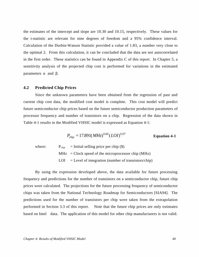
Chapter 4: Results of Modified VHSIC Model 40
the estimates of the intercept and slope are 10.30 and 10.15, respectively. These values for
the t-statistic are relevant for nine degrees of freedom and a 95% confidence interval.
Calculation of the Durbin-Watson Statistic provided a value of 1.83, a number very close to
the optimal 2. From this calculation, it can be concluded that the data are not autocorrelated
in the first order. These statistics can be found in Appendix C of this report. In Chapter 5, a
sensitivity analysis of the projected chip cost is performed for variations in the estimated
parameters α and β.
4.2 Predicted Chip Prices
Since the unknown parameters have been obtained from the regression of past and
current chip cost data, the modified cost model is complete. This cost model will predict
future semiconductor chip prices based on the future semiconductor production parameters of
processor frequency and number of transistors on a chip. Regression of the data shown in
Table 4-1 results in the Modified VHSIC model is expressed as Equation 4-1:
P MHz LOIchip = 17891 0 66 0 07. ( ) ( ). . Equation 4-1
where: Pchip = Initial selling price per chip ($)
MHz = Clock speed of the microprocessor chip (MHz)
LOI = Level of integration (number of transistors/chip)
By using the expression developed above, the data available for future processing
frequency and predictions for the number of transistors on a semiconductor chip, future chip
prices were calculated. The projections for the future processing frequency of semiconductor
chips was taken from the National Technology Roadmap for Semiconductors [SIA94]. The
predictions used for the number of transistors per chip were taken from the extrapolation
performed in Section 3.3 of this report. Note that the future chip prices are only estimates
based on Intel data. The application of this model for other chip manufacturers is not valid.
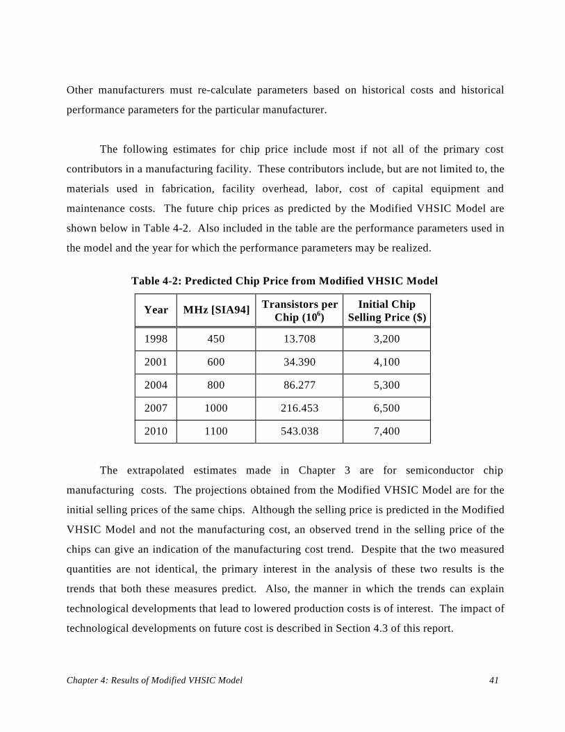
Chapter 4: Results of Modified VHSIC Model 41
Other manufacturers must re-calculate parameters based on historical costs and historical
performance parameters for the particular manufacturer.
The following estimates for chip price include most if not all of the primary cost
contributors in a manufacturing facility. These contributors include, but are not limited to, the
materials used in fabrication, facility overhead, labor, cost of capital equipment and
maintenance costs. The future chip prices as predicted by the Modified VHSIC Model are
shown below in Table 4-2. Also included in the table are the performance parameters used in
the model and the year for which the performance parameters may be realized.
Table 4-2: Predicted Chip Price from Modified VHSIC Model
Year MHz [SIA94] Transistors perChip (106)
Initial ChipSelling Price ($)
1998 450 13.708 3,200
2001 600 34.390 4,100
2004 800 86.277 5,300
2007 1000 216.453 6,500
2010 1100 543.038 7,400
The extrapolated estimates made in Chapter 3 are for semiconductor chip
manufacturing costs. The projections obtained from the Modified VHSIC Model are for the
initial selling prices of the same chips. Although the selling price is predicted in the Modified
VHSIC Model and not the manufacturing cost, an observed trend in the selling price of the
chips can give an indication of the manufacturing cost trend. Despite that the two measured
quantities are not identical, the primary interest in the analysis of these two results is the
trends that both these measures predict. Also, the manner in which the trends can explain
technological developments that lead to lowered production costs is of interest. The impact of
technological developments on future cost is described in Section 4.3 of this report.
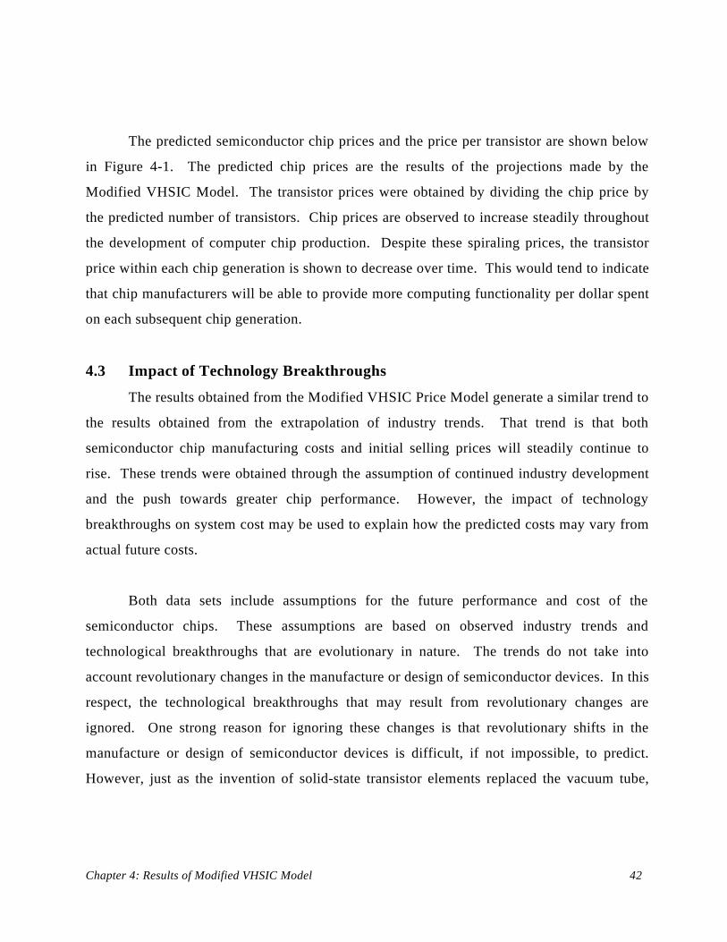
Chapter 4: Results of Modified VHSIC Model 42
The predicted semiconductor chip prices and the price per transistor are shown below
in Figure 4-1. The predicted chip prices are the results of the projections made by the
Modified VHSIC Model. The transistor prices were obtained by dividing the chip price by
the predicted number of transistors. Chip prices are observed to increase steadily throughout
the development of computer chip production. Despite these spiraling prices, the transistor
price within each chip generation is shown to decrease over time. This would tend to indicate
that chip manufacturers will be able to provide more computing functionality per dollar spent
on each subsequent chip generation.
4.3 Impact of Technology Breakthroughs
The results obtained from the Modified VHSIC Price Model generate a similar trend to
the results obtained from the extrapolation of industry trends. That trend is that both
semiconductor chip manufacturing costs and initial selling prices will steadily continue to
rise. These trends were obtained through the assumption of continued industry development
and the push towards greater chip performance. However, the impact of technology
breakthroughs on system cost may be used to explain how the predicted costs may vary from
actual future costs.
Both data sets include assumptions for the future performance and cost of the
semiconductor chips. These assumptions are based on observed industry trends and
technological breakthroughs that are evolutionary in nature. The trends do not take into
account revolutionary changes in the manufacture or design of semiconductor devices. In this
respect, the technological breakthroughs that may result from revolutionary changes are
ignored. One strong reason for ignoring these changes is that revolutionary shifts in the
manufacture or design of semiconductor devices is difficult, if not impossible, to predict.
However, just as the invention of solid-state transistor elements replaced the vacuum tube,
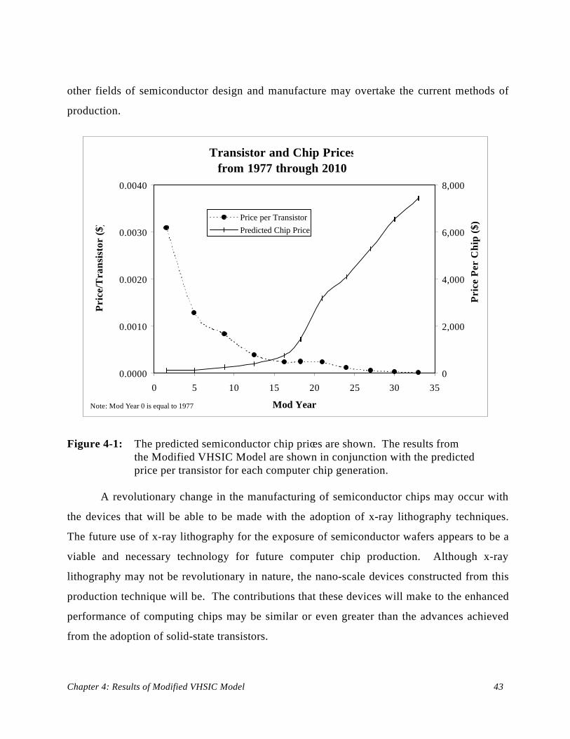
Chapter 4: Results of Modified VHSIC Model 43
other fields of semiconductor design and manufacture may overtake the current methods of
production.
Transistor and Chip Prices from 1977 through 2010
0.0000
0.0010
0.0020
0.0030
0.0040
0 5 10 15 20 25 30 35
Mod Year
Pri
ce P
er C
hip
($)
0
2,000
4,000
6,000
8,000
Note: Mod Year 0 is equal to 1977
Pri
ce/T
rans
isto
r ($
)
Price per TransistorPredicted Chip Price
Figure 4-1: The predicted semiconductor chip prices are shown. The results from the Modified VHSIC Model are shown in conjunction with the predicted price per transistor for each computer chip generation.
A revolutionary change in the manufacturing of semiconductor chips may occur with
the devices that will be able to be made with the adoption of x-ray lithography techniques.
The future use of x-ray lithography for the exposure of semiconductor wafers appears to be a
viable and necessary technology for future computer chip production. Although x-ray
lithography may not be revolutionary in nature, the nano-scale devices constructed from this
production technique will be. The contributions that these devices will make to the enhanced
performance of computing chips may be similar or even greater than the advances achieved
from the adoption of solid-state transistors.
Chapter 4: Results of Modified VHSIC Model 44
The impact of these developments on the cost experienced by manufacturers is
explored in a field called technology forecasting which deals with the impact that technology
breakthroughs may have on future performance characteristics and system cost. Figure 2-3
(on page 25) demonstrates that technology breakthroughs can have economic and technologic
effects on the manufacturing cost of a product. The possible economic benefits of technology
breakthroughs are that computing costs may be lowered through enhanced manufacturing
techniques. This may not mean that chip prices will decrease, but the overall cost per
electronic function will decrease. This effect is clearly shown in Figure 4-1 where chip prices
are observed to increase with time, but the price per transistor is observed to sharply decrease.
Therefore, the advent of computing technology based on the limitations currently being
experienced will not only lead to enhanced performance characteristics, but also to more
computing power at a lower price per transistor.
4.4 Summary
The modifications that were made to the VHSIC Price Model were used to predict
future semiconductor chip prices. To perform the estimates of future prices, the unknown
parameters were estimated and future performance parameters were placed in the model. The
future chip prices predicted by the Modified VHSIC Model were summarized in Table 4-2.
The estimated price per chip and the price per transistor were shown in Figure 4-1.
Despite the steady increase in chip price, the price per transistor was observed to
decrease for successive semiconductor chip generations. This observation would indicate that
manufacturers will continue to provide greater computing function at a lower cost per
transistor. Finally, the impact of technology breakthroughs is explored for advancements in
manufacturing and design technologies. Technology breakthroughs may contribute to lower
chip costs as a result of revolutionary changes in the design and manufacture of chips.
Chapter 5: Analysis of Predicted Prices 45
CHAPTER 5
ANALYSIS OF PREDICTED PRICES
In this chapter, the results of the Modified VHSIC Price Model are analyzed. The
sensitivity of the initial selling price is considered with respect to the technical and estimated
parameters of the model. As each parameter of the model is varied by ± 50%, the initial
selling price is computed. A profit-time equation is also developed in this chapter based on
the equations previously determined. This profit-time equation shows the initial selling price
and the manufacturing cost for any given year. The result of this equation is that the profit
margin per chip is shown to increase with each new generation of computing. The profit per
transistor, however, is shown to decrease for each year. The variation in the selling price for a
common Intel microprocessor will be shown. This graphic will illustrate that the calculated
profit margins are reasonable estimates. Finally, the impact of enhanced performance
characteristics for computing devices will be considered.
5.1 Sensitivity of Modified VHSIC Model
One-at-a-time sensitivity analysis is performed for the parameters included in the
Modified VHSIC model. This sensitivity analysis shows the difference in the chip selling
price for ± 50% changes in each parameter of the model. Equation 4-1, for which the
parameters are modified, is given below:
P MHz LOIchip = 17 891 0 66 0 07. ( ) ( ). .
In the sensitivity analysis, five parameters were modified. These parameters are α,
MHz, β, LOI, and the exponent for LOI (0.07). Two parameters were technical (MHz and
LOI), two other parameters (α and β) were determined from the linear regression of the model
performed in Chapter 3 and the last parameter is the constant exponent of the LOI term (0.07).
Chapter 5: Analysis of Predicted Prices 46
Graphs of the price sensitivity for changes in the technical and estimated parameters are given
in Appendix D of this report. For each graph, the sensitivity of the selling price is given for
years 1998, 2004, and 2010.
Between the two technical parameters (MHz and LOI), the selling price of the chip
largely depends on the processing frequency of the chip. The selling price of the chip
increased by a factor of 2 within the ± 50% range for the MHz sensitivity. Varying the LOI
factor from -50% to +50% resulted in only an 8% increase in the selling price of the chips.
Variations in the exponent of the LOI term resulted in significant increases in the initial chip
selling price as compared to changes in the MHz and LOI terms. Within the ± 50% range for
the LOI exponent, the initial selling price almost increased by a factor of 4. For analyses
where more data are available, multiple regression should be performed to more accurately
determine the value of the LOI exponent.
Between the estimated model parameters α (the constant multiplicative factor) and β
(the exponent for the MHz parameter), the selling price was more dependent on β. Although
the price almost tripled by varying α through the ± 50% range, β was more affected. For
-50% variance in the β parameter, the chip price in 2004 was merely $584. By increasing the
value of β by 50% the chip price rose to over $48,000.
5.2 Profit-Time Equations for Nanoelectronics
In this section, the cost and price equations previously constructed in Chapters 3 and 4
will be analyzed. This analysis will consist of the derivation of two profit prediction models
that are a function of time. These models are different from the Modified VHSIC Price
Model in that the previous model is a function of the performance parameters of a
semiconductor chip. The first model that will be derived is a profit-time equation on a per-
chip basis. The second model will consider profits on a per-transistor basis.
Chapter 5: Analysis of Predicted Prices 47
5.2.1 Chip Profit Equation
In Chapter 4, an equation was determined based on historical information from Intel
Microprocessor chips. By taking the natural log of both sides of Equation 4-1, the following
equation results:
ln ln . ln( ) . ln( )price MHz LOI= + +17.891 0 66 0 07 Equation 5-1
In order to determine the profit, the manufacturing cost of the chips must be
considered. The manufacturing cost per chip was determined in Chapter 3 and is expressed in
Equation 3-5:
log ( ) . . * (mod )10 1 3711 0 0265C yearchip = +
In order to derive an equation for price based only on the year, a relationship must be
established for the technical parameters and the year. Such a relationship was found in
Chapter 3 for the LOI term. The reader should recall that the (mod year) term of these
expressions uses 1977 as year 0, 1980 as year 3, and so on. Equation 3-4 states:
log ( ) . * (mod )10 4.3407 0 1332LOI year= +
A relationship between the MHz term and the year has yet to be determined.
However, the data previously used to determine the estimated parameters of the Modified
VHSIC Model can be used to find this relationship. By performing a regression analysis of
the MHz data, Equation 5-2 was formed. Regression statistics can be found in Appendix E of
this report.
ln . . (mod )MHz year= +1 022 0 1985 Equation 5-2
By combining Equations 3-4, 3-5, 5-1, and 5-2, the following relationship for the
profit per chip was obtained:
Chapter 5: Analysis of Predicted Prices 48
profit echipyear year
year
=
−
+ + +
+
( . . ( m o d ) . ln( ( . . ( m o d )) ))
( . . ( m o d ))
3 5588 0 131 0 07 10 4 3407 0 1332
1 3711 0 026510 Equation 5-3
A graph of Equation 5-3 is shown in Appendix E of this report. The result of this
equation is that the profit margin per chip is shown to increase with each new generation of
computing. As expected, the graph of this equation is almost identical to the solid line shown
in Figure 4-1 of this report. Figure 4-1 was generated using specific data from the production
of Intel Microprocessor Chips. The contribution that this equation gives is that it expresses
the profit per chip solely as a function of the year for future computing processors.
5.2.2 Transistor Profit Equation
To determine the relationship for profit on a per transistor basis, the equations for
selling price and manufacturing cost per transistor must be determined. In Chapter 3 a
relationship for the cost per transistor was found. This relationship was stated in Equation
3-2:
log ( ) . . * (mod )10 2 0304 01067C yeartrans = −
With the data used previously to determine the parameters α and β, a relationship was
obtained for the selling price per transistor. The regression statistics for this equation can be
found in Appendix E of this report.
ln . . )P yeartrans = − −5 663 0 154(mod Equation 5-4
By combining the equations stated above, the following relationship for the profit per
transistor is obtained:
profit etransyear year= −− − −( . . (mod )) ( . . (mod )5 663 0 154 2 0304 1 06710 Equation 5-5
Chapter 5: Analysis of Predicted Prices 49
The result of this equation is that the profit margin per transistor is shown to decrease
with each new generation of computing. As expected, the graph of this equation is also
nearly identical to the dashed line shown in Figure 4-1 of this report. Figure 4-1 was
generated using specific data from the production of Intel Microprocessor Chips. The
contribution that this equation gives is that it expresses the profit per transistor solely as a
function of the year for future computing processors.
5.3 Price-Drop Analysis
An analysis of the selling price for the Intel chips reveals that there is a significant
price-drop throughout the life of the chip. This price-drop may indicate that the profit
margins in the semiconductor industry are quite large. The predictions made by Equation 5-3
indicate that the ratio of initial selling price and manufacturing cost can sometimes be as high
as forty (40). This number may seem to be unreasonably high, but the reader should consider
the historical pricing performance of Intel chips. Shown in Figure 5-1 is the historical
selling price of a popular Intel chip introduced in April 1989. The initial selling price of the
486 DX 25 MHz microprocessor was $950. New, high-performance chips decreased the
demand for the chip after several years. As demand decreased so did the price until the
steady-state selling price of $102 per chip was achieved in Q1 1995.
Chapter 5: Analysis of Predicted Prices 50
Pricing History of Intel 486 DX 25 MHz Microprocessor
0
200
400
600
800
1000
1989 1990 1991 1992 1993 1994 1995Year
Pri
ce ($
)
Figure 5-1: The historical selling price for the Intel 486 DX 25 MHz chip is shown. The selling price is observed to decrease by almost a factor of 10 throughout the useful life of the chip. Note the sharp decrease in price in the middle of 1991 as a result of the introduction of the Intel 486 DX 50 MHz chip.
5.4 Enhanced Computing
At this time, there are developments in the research of computing that may lead to
revolutionary advances. These advances may lead to enhanced computing devices that will
be able to solve previously unsolved problems. Just as the advent of the solid-state transistor
revolutionized computing, a new transistor design or manufacturing process may break the
trends extrapolated in this report. These technology breakthroughs may serve to decrease the
manufacturing cost or may increase the functionality of the computing chip.
Chapter 6: Conclusions and Recommendations 51
CHAPTER 6
CONCLUSIONS AND RECOMMENDATIONS
This report has attempted to quantify manufacturing costs and initial selling prices for
the future production of more advanced transistor electronics. These estimates have been
obtained through the use of trend extrapolation, technology forecasting, and a modified
parametric price model. The conclusions of this research are as follows:
• Extrapolation of transistor cost trends showed that the price per electronic
component will continue to decrease at a rate of 50% every three years. This
extrapolation was performed using regression analysis and was statistically verified
using correlation coefficients and t-statistics.
• Extrapolation of chip transistor content showed that the level of integration will
double every three years. This estimate is a conservative estimate when compared to
Moore’s Law. This extrapolation was performed using regression analysis and was
statistically verified using correlation coefficients and t-statistics.
• Manufacturing costs for semiconductor chips will continue to rise approximately 6%
per year. This estimate is based on the continuation of the trends extrapolated for
transistor cost and transistor content.
• Modification of a generalized parametric cost model yielded a useful price model for
the prediction of future chip selling prices.
Chapter 6: Conclusions and Recommendations 52
• Future chip selling prices will increase at a rate of approximately 8% per year over
the next 15 years. This estimate is based on the continuation of established
microelectronics industry trends and technology forecasting.
• Profit-time equations were developed that predict industry profits on a per-chip and
per-transistor basis. Chip profits were observed to increase at roughly the same rate
of selling prices, and transistor profits were observed to decrease at roughly the same
rate of selling prices.
6.1 Relevance
Despite the decrease in transistor costs predicted in this report, this work anticipates
that the costs associated with facility and equipment development will continue to skyrocket!
These spiraling costs will necessitate more cost-effective solutions for the manufacture of
future computing devices.
One such proposal is the implementation of x-ray lithography for the fabrication of
chips that take advantage of the limitations currently being encountered. Although x-ray
lithography will not be feasible for industrial use until several years, or decades in the future,
it may offer a means to overcome some of the cost-hurdles for future computer chip
manufacture. In order for industry to further justify capital investment decisions, cheaper
methodologies for manufacture of computer chips must be implemented, or performance of
these chips must continue to increase at a faster rate than costs.
6.2 Recommendations for Future Research
The Modified VHSIC Price Model only considers two technical parameters for the
estimation of initial chip selling price. These two parameters are the processing speed of the
chip (MHz) and the number of transistors on the chip (LOI). Other factors such as the
minimum feature size of the chip and the bus width may be critical metrics in the estimation
Chapter 6: Conclusions and Recommendations 53
of future costs. Future research may consider the inclusion of more technical parameters to
generate a more complete model.
Validation of the Modified VHSIC Model has yet to be performed. Validation of this
model might be performed by using data available from a chip manufacturer such as
Motorola. Motorola may be a good choice for model validation because the primary focus of
chip development is similar to Intel Corporation. In addition, Motorola’s manufacturing
progress in the number of transistors per chip has been nearly identical to the Intel
Corporation [Hutch96]. An even more accurate model could also be formulated by using data
from both companies.
The results produced in this report apply strictly to the silicon-based microprocessor
computing industry. Other technologies such as gallium arsenide, memory, and application
specific integrated circuits (ASICs) have not been considered herein.
References 54
REFERENCES
ESTIMATION OF FUTURE MANUFACTURING COSTSFOR NANOELECTRONICS TECHNOLOGY
[Alde94] Adleman, L., “Molecular Computation of Solutions to Combinatorial Problems,” Science, Vol. 266, November 11, 1994, 1021-3.
[Bagg92] Baggot, J., The Meaning of Quantum Theory: A Guide for Students of Chemistry and Physics , Oxford U. Press, Oxford, 1992.
[Bate88] Bate, R. T., “The Quantum-Effect Device: Tomorrow’s Transistor?,” Scientific American, March 1988, p. 96-100.
[Brig68] Bright, J. R., Technological Forecasting for Industry and Government: Methods and Applications, Prentice-Hall, Inc., New Jersey, 1968.
[Bro75] Brock, G. W., The U.S. Computer Industry: A Study of Market Power, Ballinger Publishing Company, Cambridge, Mass., 1975.
[Cast94] Castrucci, P., Griffin, J., and Williams, M., “Design of Single Wafer Future Logic Labs,” 1994 IEEE/SEMI Advanced Semiconductor Manufacturing Conference, pp. 1-6.
[Drex92] Drexler, K. E., Nanosystems: Molecular Machinery, Manufacturing, and Computation, John Wiley and Sons, New York, 1992.
[Eig90] Eigler, D. M., and Schweizer, E. K., “Positioning Single Atoms with a Scanning Tunneling Microscope,” Nature, April 5, 1990, p. 524-6.
[Fout96] Foutz, Robert, Conversation with Virginia Tech Professor of Statistics, Time-Series Analyst, May 3, 1996.
[Fra71] Frank, C. R., Statistics and Econometrics, Holt, Rinehart and Winston, Inc., New York, 1971.
[Gent94] Gentili, M., Giovanella, C., and Selci, S., editors, Nanolithography: A Borderland between STM, EB, IB, and X-Ray Lithographies, NATO ASI Series E, Vol. 264, 1994.
References 55
[Hans91] Hansson, P. A., “Nanotechnology: Prospects and Policies,” Futures, October 1991, p. 849-59.
[Hess92] Hess, R. W., Nelson, J. R., Killingsworth, P. S., and Resetar, S. A., “Estimating the Cost of Advanced Technology,” RAND Report # P-7732, RAND, Santa Monica, CA, 1992.
[Horg94] Horgan, J., “Quantum Computing Creeps Closer to Reality,” Scientific American, April 1994, p.18.
[Hutch96] Hutcheson, G. D., and Hutcheson, J. D., “Technology and Economics in the Semiconductor Industry,” Scientific American, January 1996, pp. 54-62.
[Int96a] Intel Faxability, Quick Reference, Microprocessor Historical Pricing. This reference was a faxed document from Steve Short of the Intel Corporation.
[Int96b] Intel Faxability, Quick Reference, Intel Microprocessor Evolution. This reference was a faxed document from Steve Short of the Intel Corporation.
[Int96c] WWW address of Intel, “Intel Microprocessor Hall of Fame Technical Specifications,” http://www.intel.com/intel/museum/25anniv/html/hof/techspecs.htm.
[Keyes77] Keyes, R. W., “Physical Limits in Semiconductor Electronics,” Science, March 18, 1977, p. 1230-5.
[Lan69] Lanford, H. W., Technological Forecasting Methodologies: A Synthesis, American Management Association, USA, 1969.
[Lent93] Lent, C. S., Tougaw, P. D., Porod, W., and Bernstein, G. H., “Quantum Cellular Automata,” Nanotechnology, Vol 4., p. 49, 1993.
[Mart72] Martino, Joseph P., An Introduction to Technological Forecasting, Gordon and Breach Science Publishers, London, 1972.
[Monte95] Montemerlo, M. S., Love, J. C., Opiteck, G. J., Goldhaber, D. J., and Ellenbogen, J. C., “Technologies and Designs for Electronic Nanocomputers,” unpublished draft manuscript, MITRE, McLean, VA, 1995.
References 56
[Nanos95] MITRE Nanosystems Group, “Nanosystems Research Group Technical Review,” unpublished briefing and video, MITRE, McLean, VA, 1995.
[Noyce77] Noyce, R. N., “Microelectronics,” Scientific American, September 1977, pp. 62-9.
[Rock48] Rockett, F. H., “The Transistor,” Scientific American, September 1948, pp. 52-5.
[Rola91] Roland, J., “Nanotechnology: The Promise and Peril of Ultratiny Machines,” The Futurist, March-April 1991, p. 29-35.
[Rub90] Rubin, D., “Photolithography and the Bottom Line,” Microelectronic Manufacturing and Testing, December 1990, pp. 1, 9-10.
[SIA94] “The National Technology Roadmap for Semiconductors,” Semiconductor Industry Association, 1994.
[Stix95] Stix, G., “Toward ‘Point One,’” Scientific American, February 1995, pp. 90-5.
[Sull77] Sullivan, W. G., and Claycombe, W. W., Fundamentals of Forecasting, Reston Publishing Co, Reston, VA, 1977.
Appendix A: Transistor Electronics and its Future 57
APPENDIX A
TRANSISTOR ELECTRONICS AND ITS FUTURE
The following section supplements Chapter 1 by reviewing in greater depth some of
the more technical aspects associated with the further miniaturization of transistor electronics
[Monte95], [Nanos95]. In particular, the origin and fundamental concepts of the transistor are
discussed. Applications for the transistor and the advantages of a solid-state design instead of
the vacuum tube predecessor are addressed. The development and application of transistor
designs for computers and computing are highlighted. A pictorial description of the
photolithography fabrication process discussed in Section 1.3.1 is included. A full description
of the physical limitations for the miniaturization of current microelectronics designs is also
included.
As nanotechnology is being explored within several scientific fields, the research
efforts within mechanical, chemical, quantum, and electrical fields are described. Two
possible devices to be constructed on the nano-scale are described. A description of a
Scanning Tunneling Microscope as a nanoelectronic fabrication technology is discussed.
Finally, several predictions are made at the end of this chapter concerning the most likely path
of development for nanoelectronics technology.
A.1 The Transistor
This century’s most important invention, the transistor, has led to the invention of
resources that are essential to the entire population. It is the maturation of transistor
fabrication technology throughout the century that has allowed for more complex resources
based on transistor technologies. In this section, the invention of the transistor and its
development are discussed. The application of transistor, both in the past, current, and future
Appendix A: Transistor Electronics and its Future 58
are addressed. Finally, the development of the transistor for computing applications is
examined.
A.1.1 Birth of Electronics
The control of the flow of electrons within a vacuum tube is what first interested a
young electrical engineer named Lee De Forest. He found that if an electrified wire grid was
placed across a stream of electrons within the vacuum tube, the electron flow could be
interrupted, reduced, or stopped entirely [Rock48]. Also, De Forrest found that this device
could be used to “amplify” a weak current of electrons flowing in one end of the vacuum tube
to a strong current at the outgoing end of the tube [Rock48]. At the beginning of the century,
this device was used to give birth to the technology of electronics. Future developments,
however, proved to be equally significant in the growth of the electronics.
A.1.2 Vacuum Tube Modifications and Applications
Although the implementation of the vacuum tube in the electronics field was very
significant, the control of electrons within a solid-state device has proven to be advantageous
because of the miniaturization of the solid-state design. The invention of the transistor has
given birth to radio, television, radar, electron microscopes, electronic calculators, robot
manipulation, and most notably the computer. Through this modification, the complication
and delicacies of the vacuum tube have been eliminated. The transistor does not need to be
warmed up allowing the solid state device to be used immediately [Rock48]. Also the power
requirements for the transistor are very small. The utilization of more transistors within an
electronic device is also made possible through the ability of the transistor to be made less
expensive. The ability of mass production of transistors within a single device produced
some of the most significant developments within the field of computing.
Appendix A: Transistor Electronics and its Future 59
A.1.3 Development of Solid State Computing
In the early stages of the development of the microelectronics industry, the driving
force for advancement was the persistent and rapid decline of cost for a given electronic
function. As production within the industry doubled, the integrated circuit costs were
observed to decrease 20 to 30 percent [Noyce77]. The main technical barrier for industry
development was the production yield. As circuit complexity increased, the probability of
circuit defects increased. The most cost effective design resulted from a compromise between
the high assembly costs of chips with low levels of integration and the high scrap costs of
high levels of integration [Noyce77].
A.2 Semiconductor Manufacturing and its Limitations
As manufacturers attempt to create computer chips with smaller feature sizes, it
becomes more difficult for lithography hardware to precisely image the circuit pattern on the
chip. A pictorial description of the photolithography process is shown below in Figure A-1.
As with any manufacturing process, there exist limitations that affect the performance and the
yield of satisfactory products from that process. As the limitations that were previously
experienced for photolithography were overcome, several new limitations have emerged. A
brief description of these additional obstacles is included in this section of the Appendix.
A.2.1 Semiconductor Manufacturing
Processes for the fabrication of microprocessors have been dominated by
photolithography. Photolithography is a printing process similar to “screen printing” for the
application of designs on a T-shirt. The lithography printing process was first invented in the
18th Century by a German map inspector [Stix95]. The photolithography fabrication process
as described in Section 1.3.1 of this report is shown below in Figure A-1:
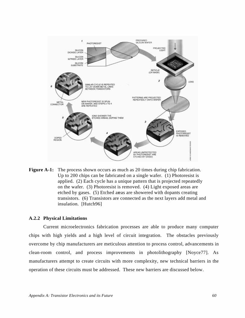
Appendix A: Transistor Electronics and its Future 60
Figure A-1: The process shown occurs as much as 20 times during chip fabrication. Up to 200 chips can be fabricated on a single wafer. (1) Photoresist is applied. (2) Each cycle has a unique pattern that is projected repeatedly on the wafer. (3) Photoresist is removed. (4) Light exposed areas are etched by gases. (5) Etched areas are showered with dopants creating transistors. (6) Transistors are connected as the next layers add metal and insulation. [Hutch96]
A.2.2 Physical Limitations
Current microelectronics fabrication processes are able to produce many computer
chips with high yields and a high level of circuit integration. The obstacles previously
overcome by chip manufacturers are meticulous attention to process control, advancements in
clean-room control, and process improvements in photolithography [Noyce77]. As
manufacturers attempt to create circuits with more complexity, new technical barriers in the
operation of these circuits must be addressed. These new barriers are discussed below.
Appendix A: Transistor Electronics and its Future 61
A.2.2.1 Wavelength of Emitted Light
Ultra-violet lithography can produce feature sizes only as small as the wavelength of
the UV light (usually 350 nanometers). To obtain greater resolution for images on the
photoresist, the wavelength of the emitted light must decrease. Semiconductor technology
has seen a steady decrease in the wavelength of emitted light used to produce chips. The
necessary decreases in the wavelength of emitted light have produced new light sources
capable of emitting light at 0.193 microns [Stix95]. Unfortunately, photoresists exposed to the
light sources capable of emitting light in the deep-ultraviolet range of the electromagnetic
spectrum (less than 0.2 microns) absorb a significant amount of the light [Stix95]. The
photoresists absorb so much of the light that it takes more time to transfer the circuit pattern to
the chip.
A.2.2.2 Lens Focus on Photoresist
As the feature sizes of the transistor become smaller, new lens systems must be
developed to reduce the image passed through the mask. Also, the ability of this image to be
focused clearly on the photoresist is affected. As a result, the aperture of the lens system must
be increased. A wide lens aperture increases the resolution but decreases the field of focus.
In fact, projected images tend to fade at distances below 1 micron [Stix95]. The inability of
the lens to focus to such precise definition on the photoresist is largely a materials problem.
The few lens materials that have been identified for the sub-0.2 micron feature size
development perform poorly [Stix95]. The fused silica glass for lenses tends to absorb the
emitted light and heat up. This increase in temperature of the lens degrades the image by
changing the angle at which the lens refracts the light.
A.2.2.3 Tunneling
Transistor components are separated from each other such that the performance of one
component will not affect the performance of the other. For greater transistor densities, the
insulation layer between components must decrease. This decrease in insulation layer size
Appendix A: Transistor Electronics and its Future 62
can affect system performance in that electrons can migrate through the insulation layer. The
migration of electrons through small energy barriers in electronic circuits is known as
tunneling. The result of tunneling is that a transistor that should normally be in an “off state”
may in fact be in an “on state” [Bagg92]. An insulation layer more resistant to tunneling may
be achieved through the development of materials with a lower dielectric constant.
A.2.2.4 Heat Dissipation
Current microprocessor chips, such as Intel’s Pentium chip, contain over 3.2 million
transistors [SIA94]. While the amount of transistors on a chip has dramatically increased, the
size of a computer chip has remained relatively unchanged. The density of components on a
chip has a dramatic effect on the heat that must be dissipated from the surface of the chip. If
not for cooling fins on the surfaces of today’s microprocessors, many of them would melt
themselves down. Conventional transistor designs are eventually going to be limited in
density based on the ability of chip manufacturers to siphon heat from the surface of the chip
[Keyes77].
A.3 Nanotechnology
Although this project focuses on the development of nanotechnology from the
perspective of electronics and computer electronics development, nanotechnology is being
explored in many fields of research. The following section will describe some of the
implementation technologies for the development of nanotechnology. The devices that are
being proposed for the construction of nanoelectronic circuits are also described. Finally, the
use of x-ray lithography and Scanning Tunneling Microscope (STM) for the fabrication of
nanoelectronic circuits will be highlighted.
A.3.1 Implementation Technologies
Nanotechnology has proven to be a very diverse field that may obtain applications
within the fields of biology, materials, transportation, communications, and computing. In no
Appendix A: Transistor Electronics and its Future 63
other field, however, has there been more interest in the possibilities of nanotechnology than
computing. As the minimum feature size within computing devices has decreased, limitations
in fabrication techniques have been and continue to be an obstacle for future miniaturization.
The technology that will contribute to the development of nano-computing could arise from
quantum, mechanical, chemical, and electronic technologies. In this section, each of these
technologies is discussed and the advantages and disadvantages for each of these technologies
is considered.
A.3.1.1 Quantum
For the development of computing devices based on the quantum nature of matter, the
natural mechanism of interference of quantum waves associated with nano-scale components
could be used to perform parallel computations [Bagg92]. Proposed quantum computers
would represent a bit of information as a quantum state of some component of the computer,
such as the spin orientation of an atom [Bagg92]. The development of computers based on
these types of quantum effects is still in a research phase. It is perceived, however, because
quantum devices would be very sensitive to small physical distortions and stray photons, such
devices must be carefully isolated and operated at temperatures close to absolute zero
[Bagg92]. Because quantum nanocomputers could perform massively parallel computations,
a primary interest in the application of these devices is to solve certain classes of previously
unsolved problems.
A.3.1.2 Mechanical
The notion of a mechanical device for performing calculations has existed for several
centuries. Probably the first mechanical computer was the abacus, created by the Chinese.
On the nano-scale, the implementation of a computing device was partly inspired by the
macroscopic mechanical computers created by Charles Babbage in the 1830s and 1840s.
Mechanical nanocomputers would calculate using moving molecular-scale rods and rotating
molecular-scale wheels, that spin on shafts and bearings [Drex92].
Appendix A: Transistor Electronics and its Future 64
A leading authority of nanotechnology, K. Eric Drexler, envisions that such small-
scale devices would be assembled by mechanical positioning of atoms or molecules one unit
at a time. This process is known as “mechanosynthesis”. A viable technique for
mechanosynthesis is the implementation of an STM (Scanning Tunneling Microscope). A
major disadvantage for the use of STM is that, as a manipulator of atoms one at a time,
fabrication of the even smallest device would prove to be time consuming. The development
of STM arrays, however, can provide the ability to build nano-scale components in parallel
[Drex92].
A.3.1.3 Chemical
The ability of making and breaking bonds which process information is the idea
behind a chemical computer. Logic states and information are contained within the resulting
chemical structure. Proponents of “biochemically-based” computers point to an existence
proof that performs computations through the multi-cellular nervous system of humans and
other animals. Despite the difficulties in reproducing a living computational system, there has
been some evidence of the use of chemical systems for the solution to specific problems. A
scientist named Adleman used fragments of DNA to compute the solution to a complex graph
theory problem [Adle94]. The greatest potential for application of chemical computations lies
in the realm of combinatorial type problems.
A.3.1.4 Electrical
The development of electronic-based computing elements spans over 50 years. The
large infrastructure that has already miniaturized circuit elements is the most poised and
mature industry to develop and fabricate nano-scale components. As electronics-based
computers have become more popular, the demands for faster and more powerful devices
continues to increase. As Figure 1-1 has shown, the rate of increase in the density of
transistors on a single chip is exponential. Over that time span, and up to the present, the
Appendix A: Transistor Electronics and its Future 65
fundamental operating principles of the transistor have remained the same. To maintain the
current rate of development and miniaturization, changes must occur in the construct of
electronic transistors. These changes will occur in manufacturing of such devices and the
structure of the components for such devices.
A.3.2 Nanoelectronic Devices
The development of an electronic nanocomputer will represent the storage and
retrieval of information by the movement of electrons. To control electrons on a nano-scale,
many of the nanodevices proposed to replace the transistor will take advantage of the
quantum effects currently experienced by shrinking of bulk-effect transistors. Two such
devices are quantum dots and Resonant Tunneling Diodes. These devices are described in the
two sections below.
A.3.2.1 Quantum Dots
Quantum dots control the tunneling of a small number of electrons through the
influence of a generated electric field. The dots have shown the capability to perform both
switching and amplification characteristics. For an electron, the quantum dot serves as a
potential well from which the electron is not free to move in any dimension. For computing
purposes, the presence or absence of an electron within the quantum dot can function as a
switch (1 or 0) [Horg94]. Some quantum dots have been fabricated to be as small as 30
nanometers.
A group at the University of Notre Dame has proposed and experimented with a
method for performing logic functions with arrays of quantum dot cells. These arrays
function as a result of the repulsion of like charges with neighboring arrays [Lent93]. This
repulsion causes adjacent quantum dot cells to line up in the same state, since the lowest
energy for the entire system is achieved in this state. By setting up the appropriate patterns
for these arrays of quantum dot cells, Boolean logic functions can be implemented [Lent93].
Appendix A: Transistor Electronics and its Future 66
Since these quantum dot arrays communicate via their electric field and not current flow, their
use as a form of wireless computation is possible.
A.3.2.2 Resonant Tunneling Diodes (RTDs)
The technology for the creation of resonant tunneling diodes has been used to fabricate
and experiment with this possible implementation of nanoelectronic devices. An RTD is
composed of two insulating barriers in a semiconductor. This creates an island as small as 10
nanometers in width between the two semiconductors [Bate88]. Whenever electrons are
confined within two such closely spaced barriers, the quantum waves properties of the
electrons restrict the particle energies to discrete energy levels. This quantization of the
electrons within energy band is the principle upon which the RTD operates [Bate88]. The
probability for the electrons to tunnel from outside the barriers is dependent on the average
energy of the incoming electrons. When the average energy of such electrons is equal to the
quantized energy levels of the device, significant tunneling can occur.
By incorporating an RTD into the emitter of a BJT (bipolar junction transistor) a
“resonant tunneling transistor” has been fabricated. This compound device is controlled by
the RTD which serves as a filter to allow current to flow into the emitter of the BJT at certain
base-emitter voltages. These gate voltages correspond to specific internal energy levels of the
RTD [Bate88]. As the base-emitter voltage increases, the current can go from an “off” state
where the base-emitter voltage does not correspond to an internal energy level of the RTD to
an “on” state where the internal energy level of the RTD matches the base-emitter voltage.
Used in this manner, the resonant tunneling transistor can be used as a two-state device
capable of computations.
A.3.3 Nanoelectronic Fabrication Technologies
Regardless of the conceptual inventions for the implementation of nano-scale
electronic devices, their eventual application and adoption into mainstream electronics will
Appendix A: Transistor Electronics and its Future 67
depend on the fabrication technologies that can build such devices. As conventional
lithography techniques are becoming more expensive and complicated, new manufacturing
technologies have emerged. Also, the modification of existing lithography technologies has
been explored for the fabrication of electronic devices on the nano-scale. Two such
technologies are discussed in this section.
A.3.3.1 X-Ray Lithography
As semiconductor chip manufacturers move towards smaller wavelengths of the light
spectrum, the available visible wavelengths that can be used for the fabrication of
microelectronics circuits decreases. This limit has caused several researchers in the
microelectronics field to research non-visible forms of electromagnetic waves for lithography.
A brief description of x-ray lithography is included in Section 1.3.3.1 of this report.
A.3.3.2 STM
A radically different method for the manipulation of atoms or molecules has been
proposed. This method involves mechanosynthesis through the use of an STM (Scanning
Tunneling Microscope). An early example for the use of an STM was the work performed by
Eigler and Schweitzer at IBM. This pair used the microscope to position atoms to spell
“IBM” [Eig90]. The STM uses a sharp tungsten tip through which a few tenths of a volt can
pass to a conducting sample. Tunneling of atoms from the surface of the conducting sample
to the tip can occur when the tip is close (0.5 nanometers) to touching the sample [Eig90].
For the fabrication of devices based on STM technology, the tip voltage can be
adjusted such that a covalently-bonded atom can move from the surface to the tip. Removal
of the atom from the tip can be performed by adjusting the tip voltage. A major problem for
the permanent placement of the atoms on the surface of the sample is that at high
temperatures the atom may tend to migrate [Eig90], thus altering the structure originally
created. The “IBM” that Eigler and Schweitzer created was performed at temperatures near
Appendix A: Transistor Electronics and its Future 68
zero degrees Kelvin. For manipulation of a greater quantity of atoms, an STM array has also
been proposed. This device is similar to an STM, however, an array of tips has been
constructed to manipulate the atoms on an atomic scale. At this point, STM technology is still
very developmental and fabrication has proven to be a very time consuming process.
A.4 Nanoelectronic Developments
As can be seen from this section, the development and progress within the transistor-
based electronics industry has been nothing short of phenomenal. The developments that
have occurred over the past five decades have provided the world with more computational
power than ever considered possible. The steady development of the electronics industry is
also expected to continue well into the next century. To maintain the same rate of
development, new technologies must be implemented to overcome the physical and economic
barriers that are currently being experienced. These new technologies are expected to take
advantage of the current limitations of microelectronics device fabrication. Nanoelectronics
development will not only take advantage of these limitations, but may provide enhanced
operational characteristics.
Modifications to the lithography process may produce nano-scale devices with high
product yield and high reliability. One particular lithography method of interest is x-ray
lithography. This technology is limited by the depth of field for the x-rays and the cost of the
synchrotrons necessary to generate the x-rays. Also necessary for the successful large-scale
development of x-rays are masks and photoresists used in the processing of the chips. The
ability of these devices to produce very small minimum feature sizes is the greatest advantage
of this technology. The possibility for x-ray devices to produce nano-scale devices for large
scale production of electronic devices has been the primary consideration of this research.
Appendix B: Regression Statistics for Time-Series Data 69
APPENDIX B
REGRESSION STATISTICS FORTIME-SERIES DATA
On the following two pages are the statistics for the regression performed in Chapter 3
of this report. The current cost data and predicted future costs are shown in Table B-1. The
current and future chip transistor content is shown in Table B-2.
Statistical analysis to test the data for auto-correlation was performed using the
Durbin-Watson, linear first-order autocorrelation. The data used for the analysis as well as
the output from the calculation is shown on the last two pages of Appendix B.
Appendix B: Regression Statistics for Time-Series Data 70
Table B-1: Least-Squares Linear Regression of Transistor Cost Data
Year ModYear
Observed Cost(millicents)
Observed CostLog(10) Cost
Regression ResultsLog(10) Cost
Predicted Cost(millicents)
1977 0 112 2.049 2.030 107.251980 3 47 1.672 1.710 51.311983 6 24 1.380 1.390 24.551986 9 13.5 1.130 1.070 11.741989 12 5.2 0.716 0.750 5.6181992 15 2.7 0.431 0.429 2.6871995 18 - - 0.109 1.2861998 21 - - -0.211 0.6152001 24 - - -0.531 0.2942004 27 - - -0.852 0.1412007 30 - - -1.172 0.0672010 33 - - -1.492 0.032
SUMMARY OUTPUT
Regression StatisticsMultiple R 0.99814R Square 0.99628Adj. R Square 0.99535Standard Error 0.04092Observations 6
ANOVAdf SS MS F Significance F
Regression 1 1.79438 1.79438 1071.490 5.194E-06Residual 4 0.00670 0.00167Total 5 1.80108
Coefficients Standard Error t Stat P-valueIntercept 2.0304 0.0296 68.5539 271.27E-9X Variable 1 -0.1067 0.0033 -32.7336 5.19E-6
Lower 95% Upper 95%1.9482 2.1126-0.1158 -0.0977
Appendix B: Regression Statistics for Time-Series Data 71
Table B-2: Least-Squares Linear Regression of Transistor Content Data
Year ModYear
ObservedTransistors (N)
Observed NLog(10) N
Regression ResultsLog(10) N
Predicted N
1978 1.5 29,000 4.4624 4.5404 34.71E+31982 5 134,000 5.1271 5.0065 101.50E+31985 8.8 275,000 5.4393 5.5125 325.43E+31989 12.5 1,200,000 6.0792 6.0051 1.01E+61993 16.25 3,100,000 6.4914 6.5045 3.19E+61995 18.25 5,500,000 6.7404 6.7708 5.90E+61998 21 - - 7.1370 13.71E+62001 24 - - 7.5364 34.39E+62004 27 - - 7.9359 86.28E+62007 30 - - 8.3354 216.45E+62010 33 - - 8.7348 543.04E+6
SUMMARY OUTPUT
Regression StatisticsMultiple R 0.99568R Square 0.99138Adj. R Square 0.98922Standard Error 0.09023Observations 6
ANOVAdf SS MS F Significance F
Regression 1 3.74438 3.74438 459.877 28.0E-6Residual 4 0.03257 0.00814Total 5 3.77695
Coefficients Standard Error t Stat P-valueIntercept 4.3407 0.0743 58.4568 512.82E-9X Variable 1 0.1332 0.0062 21.4447 27.96E-6
Lower 95% Upper 95%4.1345 4.54690.1159 0.1504
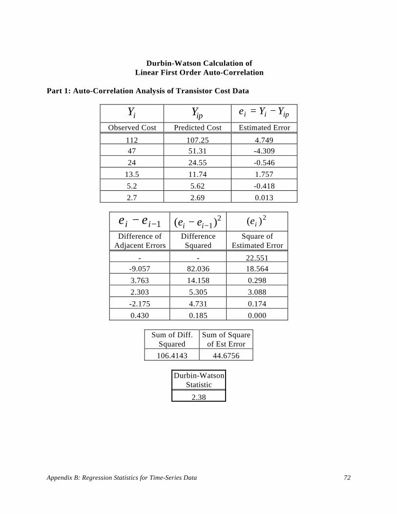
Appendix B: Regression Statistics for Time-Series Data 72
Durbin-Watson Calculation ofLinear First Order Auto-Correlation
Part 1: Auto-Correlation Analysis of Transistor Cost Data
Yi Yip e Y Yi i ip= −Observed Cost Predicted Cost Estimated Error
112 107.25 4.74947 51.31 -4.30924 24.55 -0.546
13.5 11.74 1.7575.2 5.62 -0.4182.7 2.69 0.013
e ei i− −1 ( )e ei i− −12 ( )ei
2
Difference ofAdjacent Errors
DifferenceSquared
Square ofEstimated Error
- - 22.551-9.057 82.036 18.5643.763 14.158 0.2982.303 5.305 3.088-2.175 4.731 0.1740.430 0.185 0.000
Sum of Diff.Squared
Sum of Squareof Est Error
106.4143 44.6756
Durbin-WatsonStatistic
2.38
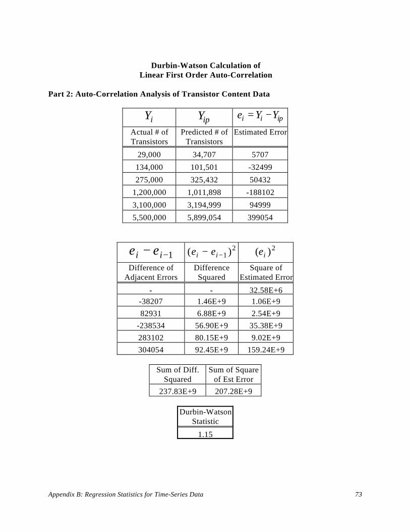
Appendix B: Regression Statistics for Time-Series Data 73
Durbin-Watson Calculation ofLinear First Order Auto-Correlation
Part 2: Auto-Correlation Analysis of Transistor Content Data
Yi Yip e Y Yi i ip= −Actual # ofTransistors
Predicted # ofTransistors
Estimated Error
29,000 34,707 5707134,000 101,501 -32499275,000 325,432 50432
1,200,000 1,011,898 -1881023,100,000 3,194,999 949995,500,000 5,899,054 399054
e ei i− −1 ( )e ei i− −12 ( )ei
2
Difference ofAdjacent Errors
DifferenceSquared
Square ofEstimated Error
- - 32.58E+6-38207 1.46E+9 1.06E+982931 6.88E+9 2.54E+9
-238534 56.90E+9 35.38E+9283102 80.15E+9 9.02E+9304054 92.45E+9 159.24E+9
Sum of Diff.Squared
Sum of Squareof Est Error
237.83E+9 207.28E+9
Durbin-WatsonStatistic
1.15
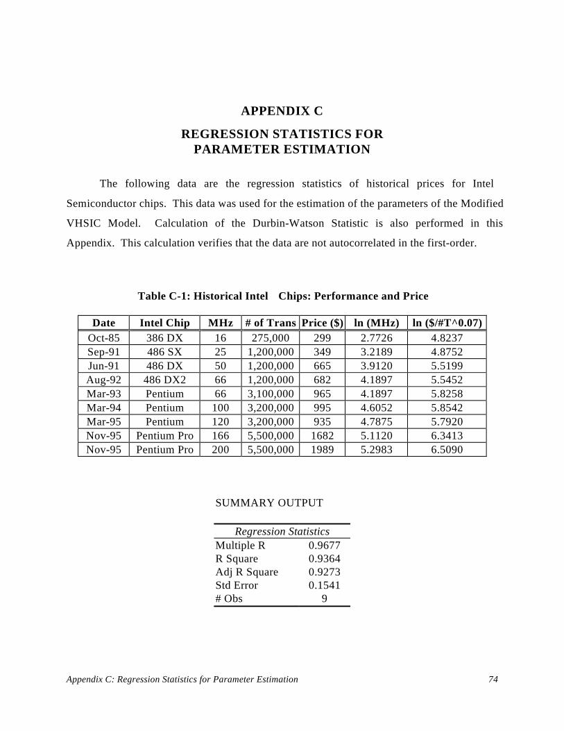
Appendix C: Regression Statistics for Parameter Estimation 74
APPENDIX C
REGRESSION STATISTICS FORPARAMETER ESTIMATION
The following data are the regression statistics of historical prices for Intel
Semiconductor chips. This data was used for the estimation of the parameters of the Modified
VHSIC Model. Calculation of the Durbin-Watson Statistic is also performed in this
Appendix. This calculation verifies that the data are not autocorrelated in the first-order.
Table C-1: Historical Intel Chips: Performance and Price
Date Intel Chip MHz # of Trans Price ($) ln (MHz) ln ($/#T^0.07)Oct-85 386 DX 16 275,000 299 2.7726 4.8237Sep-91 486 SX 25 1,200,000 349 3.2189 4.8752Jun-91 486 DX 50 1,200,000 665 3.9120 5.5199Aug-92 486 DX2 66 1,200,000 682 4.1897 5.5452Mar-93 Pentium 66 3,100,000 965 4.1897 5.8258Mar-94 Pentium 100 3,200,000 995 4.6052 5.8542Mar-95 Pentium 120 3,200,000 935 4.7875 5.7920Nov-95 Pentium Pro 166 5,500,000 1682 5.1120 6.3413Nov-95 Pentium Pro 200 5,500,000 1989 5.2983 6.5090
SUMMARY OUTPUT
Regression StatisticsMultiple R 0.9677R Square 0.9364Adj R Square 0.9273Std Error 0.1541# Obs 9
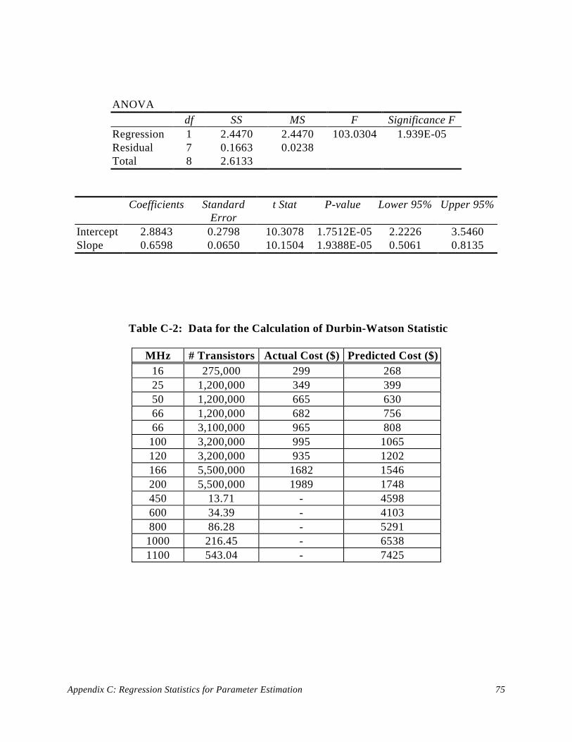
Appendix C: Regression Statistics for Parameter Estimation 75
ANOVAdf SS MS F Significance F
Regression 1 2.4470 2.4470 103.0304 1.939E-05Residual 7 0.1663 0.0238Total 8 2.6133
Coefficients StandardError
t Stat P-value Lower 95% Upper 95%
Intercept 2.8843 0.2798 10.3078 1.7512E-05 2.2226 3.5460Slope 0.6598 0.0650 10.1504 1.9388E-05 0.5061 0.8135
Table C-2: Data for the Calculation of Durbin-Watson Statistic
MHz # Transistors Actual Cost ($) Predicted Cost ($)16 275,000 299 26825 1,200,000 349 39950 1,200,000 665 63066 1,200,000 682 75666 3,100,000 965 808100 3,200,000 995 1065120 3,200,000 935 1202166 5,500,000 1682 1546200 5,500,000 1989 1748450 13.71 - 4598600 34.39 - 4103800 86.28 - 52911000 216.45 - 65381100 543.04 - 7425
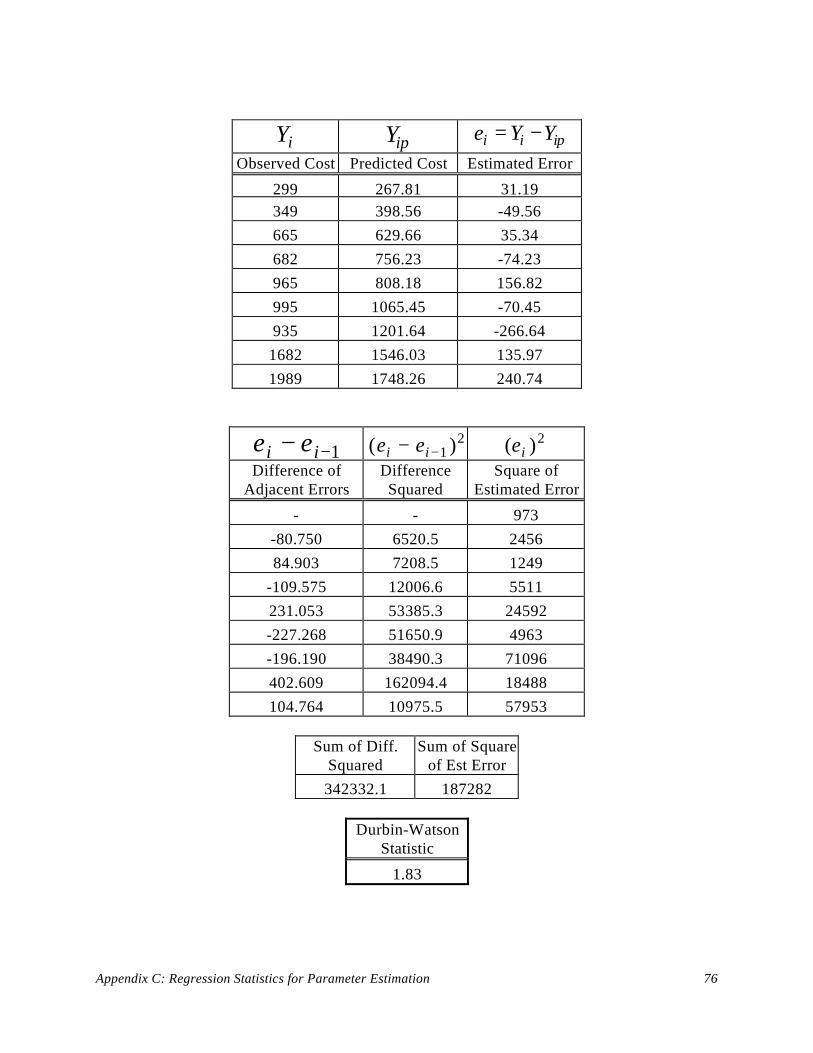
Appendix C: Regression Statistics for Parameter Estimation 76
Yi Yip e Y Yi i ip= −Observed Cost Predicted Cost Estimated Error
299 267.81 31.19349 398.56 -49.56665 629.66 35.34682 756.23 -74.23965 808.18 156.82995 1065.45 -70.45935 1201.64 -266.641682 1546.03 135.971989 1748.26 240.74
e ei i− −1 ( )e ei i− −12 ( )ei
2
Difference ofAdjacent Errors
DifferenceSquared
Square ofEstimated Error
- - 973-80.750 6520.5 245684.903 7208.5 1249
-109.575 12006.6 5511231.053 53385.3 24592-227.268 51650.9 4963-196.190 38490.3 71096402.609 162094.4 18488104.764 10975.5 57953
Sum of Diff.Squared
Sum of Squareof Est Error
342332.1 187282
Durbin-WatsonStatistic
1.83
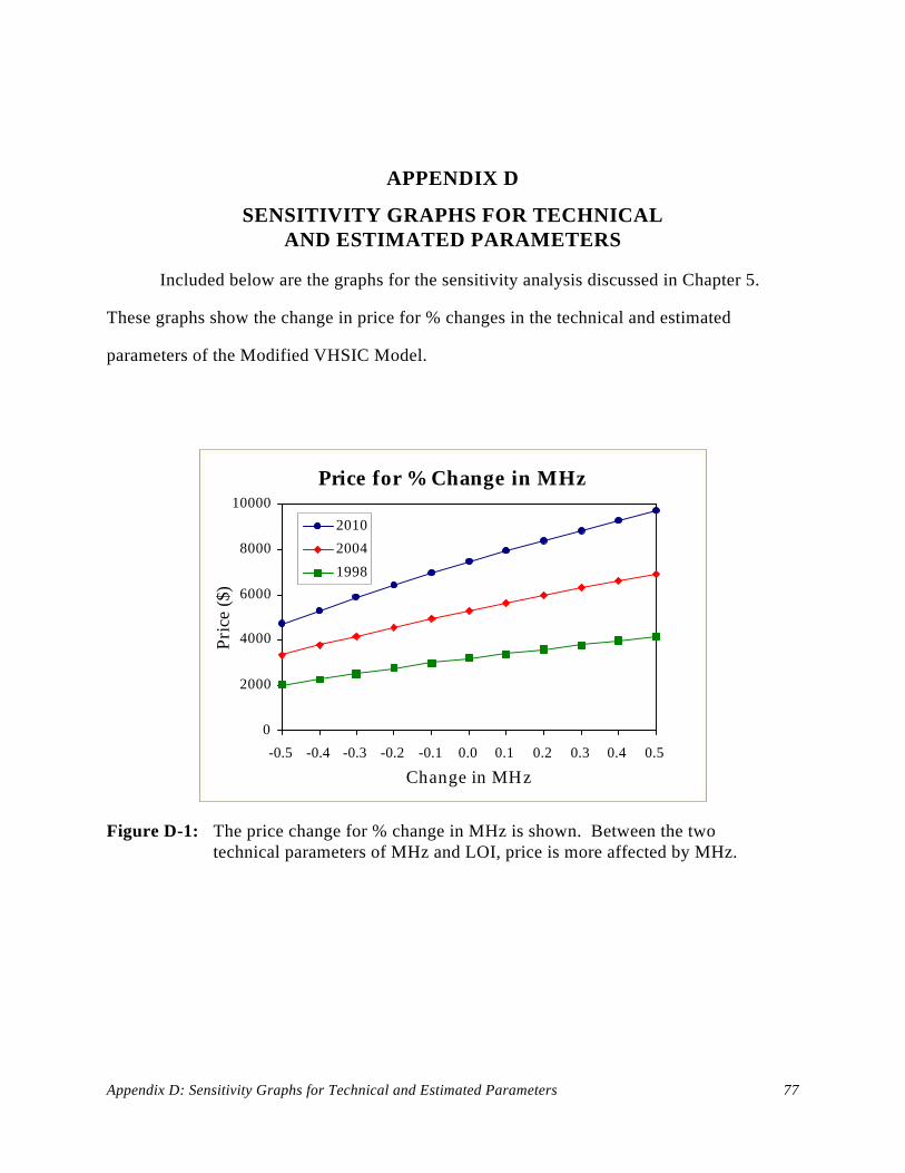
Appendix D: Sensitivity Graphs for Technical and Estimated Parameters 77
APPENDIX D
SENSITIVITY GRAPHS FOR TECHNICALAND ESTIMATED PARAMETERS
Included below are the graphs for the sensitivity analysis discussed in Chapter 5.
These graphs show the change in price for % changes in the technical and estimated
parameters of the Modified VHSIC Model.
Price for % Change in MHz
0
2000
4000
6000
8000
10000
-0.5 -0.4 -0.3 -0.2 -0.1 0.0 0.1 0.2 0.3 0.4 0.5
Change in MHz
Pric
e ($
)
2010
2004
1998
Figure D-1: The price change for % change in MHz is shown. Between the two technical parameters of MHz and LOI, price is more affected by MHz.
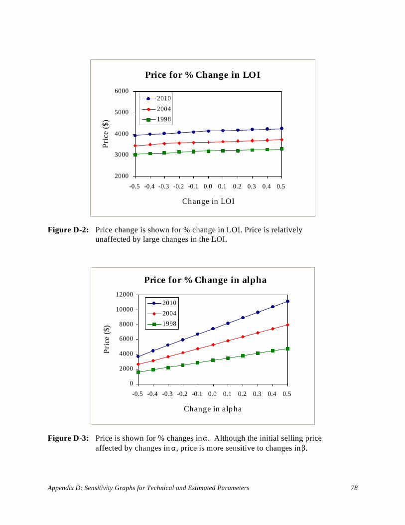
Appendix D: Sensitivity Graphs for Technical and Estimated Parameters 78
Price for % Change in LOI
2000
3000
4000
5000
6000
-0.5 -0.4 -0.3 -0.2 -0.1 0.0 0.1 0.2 0.3 0.4 0.5
Change in LOI
Pric
e ($
)2010
2004
1998
Figure D-2: Price change is shown for % change in LOI. Price is relativelyunaffected by large changes in the LOI.
Price for % Change in alpha
0
2000
4000
6000
8000
10000
12000
-0.5 -0.4 -0.3 -0.2 -0.1 0.0 0.1 0.2 0.3 0.4 0.5
Change in alpha
Pric
e ($
)
2010
2004
1998
Figure D-3: Price is shown for % changes in α. Although the initial selling price affected by changes in α, price is more sensitive to changes in β.
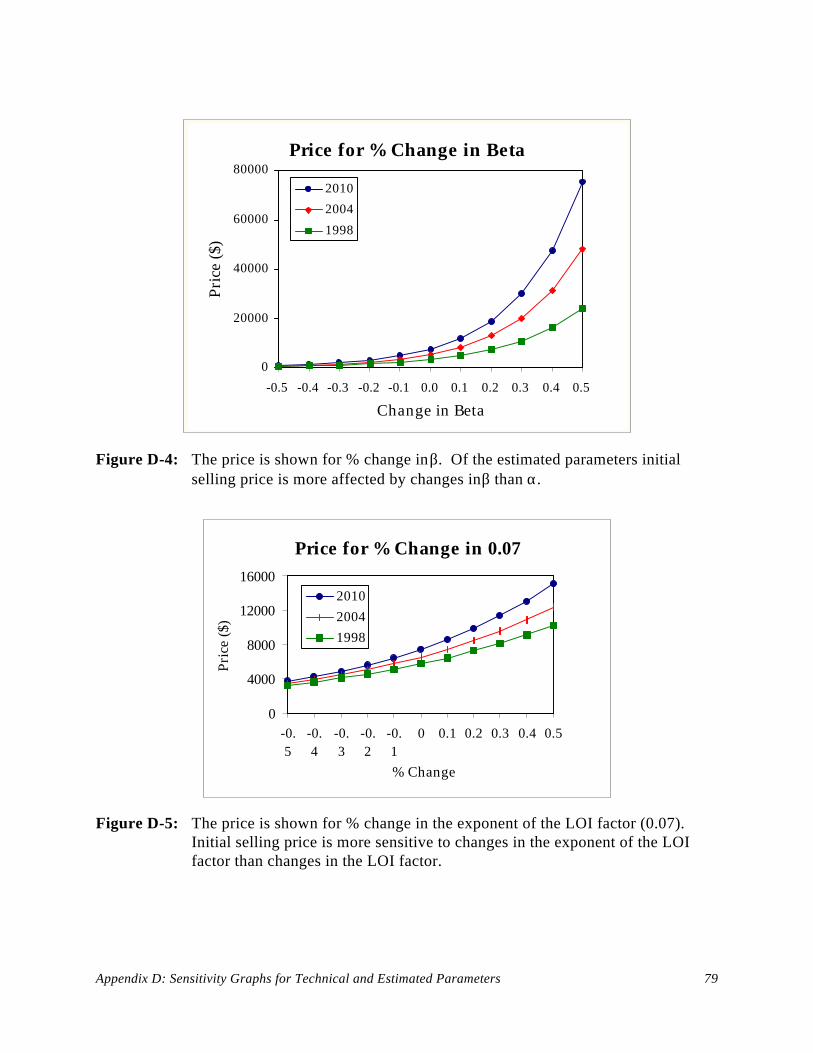
Appendix D: Sensitivity Graphs for Technical and Estimated Parameters 79
Price for % Change in Beta
0
20000
40000
60000
80000
-0.5 -0.4 -0.3 -0.2 -0.1 0.0 0.1 0.2 0.3 0.4 0.5
Change in Beta
Pric
e ($
)
2010
2004
1998
Figure D-4: The price is shown for % change in β. Of the estimated parameters initial selling price is more affected by changes in β than α.
Price for % Change in 0.07
0
4000
8000
12000
16000
-0.5
-0.4
-0.3
-0.2
-0.1
0 0.1 0.2 0.3 0.4 0.5
% Change
Pric
e ($
)
201020041998
Figure D-5: The price is shown for % change in the exponent of the LOI factor (0.07). Initial selling price is more sensitive to changes in the exponent of the LOI factor than changes in the LOI factor.
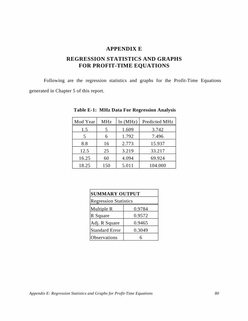
Appendix E: Regression Statistics and Graphs for Profit-Time Equations 80
APPENDIX E
REGRESSION STATISTICS AND GRAPHSFOR PROFIT-TIME EQUATIONS
Following are the regression statistics and graphs for the Profit-Time Equations
generated in Chapter 5 of this report.
Table E-1: MHz Data For Regression Analysis
Mod Year MHz ln (MHz) Predicted MHz
1.5 5 1.609 3.7425 6 1.792 7.496
8.8 16 2.773 15.93712.5 25 3.219 33.21716.25 60 4.094 69.92418.25 150 5.011 104.000
SUMMARY OUTPUTRegression Statistics
Multiple R 0.9784R Square 0.9572Adj. R Square 0.9465Standard Error 0.3049Observations 6
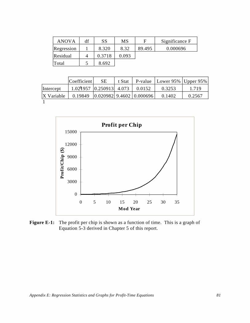
Appendix E: Regression Statistics and Graphs for Profit-Time Equations 81
ANOVA df SS MS F Significance FRegression 1 8.320 8.32 89.495 0.000696Residual 4 0.3718 0.093Total 5 8.692
Coefficients
SE t Stat P-value Lower 95% Upper 95%Intercept 1.021957 0.250913 4.073 0.0152 0.3253 1.719X Variable1
0.19849 0.020982 9.4602 0.000696 0.1402 0.2567
Profit per Chip
0
3000
6000
9000
12000
15000
0 5 10 15 20 25 30 35Mod Year
Pro
fit/
Ch
ip ($
)
Figure E-1: The profit per chip is shown as a function of time. This is a graph of Equation 5-3 derived in Chapter 5 of this report.
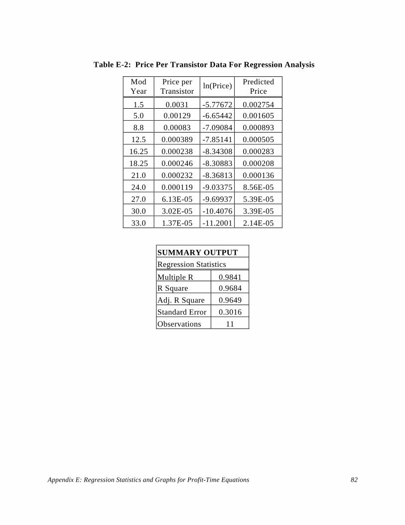
Appendix E: Regression Statistics and Graphs for Profit-Time Equations 82
Table E-2: Price Per Transistor Data For Regression Analysis
ModYear
Price perTransistor
ln(Price) PredictedPrice
1.5 0.0031 -5.77672 0.0027545.0 0.00129 -6.65442 0.0016058.8 0.00083 -7.09084 0.00089312.5 0.000389 -7.85141 0.00050516.25 0.000238 -8.34308 0.00028318.25 0.000246 -8.30883 0.00020821.0 0.000232 -8.36813 0.00013624.0 0.000119 -9.03375 8.56E-0527.0 6.13E-05 -9.69937 5.39E-0530.0 3.02E-05 -10.4076 3.39E-0533.0 1.37E-05 -11.2001 2.14E-05
SUMMARY OUTPUTRegression Statistics
Multiple R 0.9841R Square 0.9684Adj. R Square 0.9649Standard Error 0.3016Observations 11
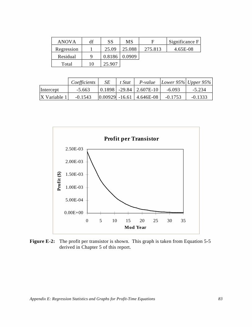
Appendix E: Regression Statistics and Graphs for Profit-Time Equations 83
ANOVA df SS MS F Significance FRegression 1 25.09 25.088 275.813 4.65E-08Residual 9 0.8186 0.0909
Total 10 25.907
Coefficients SE t Stat P-value Lower 95% Upper 95%Intercept -5.663 0.1898 -29.84 2.607E-10 -6.093 -5.234X Variable 1 -0.1543 0.00929 -16.61 4.646E-08 -0.1753 -0.1333
Profit per Transistor
0.00E+00
5.00E-04
1.00E-03
1.50E-03
2.00E-03
2.50E-03
0 5 10 15 20 25 30 35Mod Year
Pro
fit (
$)
Figure E-2: The profit per transistor is shown. This graph is taken from Equation 5-5 derived in Chapter 5 of this report.
Vita 84
VITA
Michael D. Smith was born on June 1, 1972, in Cumberland, Maryland. From 1986 to1990 he attended Bishop Walsh High School in Cumberland. He graduated fromVirginia Polytechnic Institute and State University with a Bachelors of Science Degreein Materials Science and Engineering in May of 1994. As an undergraduate, hisspecialization was electronic materials.
Mr. Smith has been in the graduate program of Industrial and Systems Engineeringsince the Fall of 1994. His concentration in the ISE Program was ManufacturingSystems Engineering. In the Summer of 1995, he worked at the MITRE Corporationas a Technology Cost Analyst. He graduated from Virginia Tech in May of 1996 witha Master of Engineering Degree. Soon thereafter he went to work at Price WaterhouseLLP as a Systems Consultant.