Embed Size (px)
Citation preview

ET2A
DN9815361Issue 5-0 en
# Nokia Corporation 1 (62)
BSC3119Nokia BSC/TCSM, Rel. S12, ProductDocumentation, v.1

The information in this document is subject to change without notice and describes only theproduct defined in the introduction of this documentation. This document is intended for the useof Nokia's customers only for the purposes of the agreement under which the document issubmitted, and no part of it may be reproduced or transmitted in any form or means without theprior written permission of Nokia. The document has been prepared to be used by professionaland properly trained personnel, and the customer assumes full responsibility when using it.Nokia welcomes customer comments as part of the process of continuous development andimprovement of the documentation.
The information or statements given in this document concerning the suitability, capacity, orperformance of the mentioned hardware or software products cannot be considered binding butshall be defined in the agreement made between Nokia and the customer. However, Nokia hasmade all reasonable efforts to ensure that the instructions contained in the document areadequate and free of material errors and omissions. Nokia will, if necessary, explain issueswhich may not be covered by the document.
Nokia's liability for any errors in the document is limited to the documentary correction of errors.NOKIA WILL NOT BE RESPONSIBLE IN ANY EVENT FOR ERRORS IN THIS DOCUMENTOR FOR ANY DAMAGES, INCIDENTAL OR CONSEQUENTIAL (INCLUDING MONETARYLOSSES), that might arise from the use of this document or the information in it.
This document and the product it describes are considered protected by copyright according tothe applicable laws.
NOKIA logo is a registered trademark of Nokia Corporation.
Other product names mentioned in this document may be trademarks of their respectivecompanies, and they are mentioned for identification purposes only.
Copyright © Nokia Corporation 2007. All rights reserved.
2 (62) # Nokia Corporation DN9815361Issue 5-0 en
ET2A
Contents
Contents 3
List of tables 4
List of figures 5
Summary of changes 7
1 ET2A overview 9
2 Capacity and performance of ET2A 13
3 Structure of ET2A 153.1 Mechanical structure of ET2A 153.2 Logical structure of ET2A 153.3 Operating principles of ET2A 183.3.1 Timing 183.3.2 Microcomputer 203.3.3 Changeover 283.3.4 Supervision of basic timing signals 283.3.5 Incoming direction 293.3.6 Outgoing direction 323.3.7 Loops 333.3.8 Maintenance interface 343.3.9 DC/DC converter 353.3.9.1 Introduction to DC/DC converter 353.3.9.2 Input circuit 373.3.9.3 Auxiliary voltage regulator 383.3.9.4 Undervoltage supervision 383.3.9.5 Frequency limitation 393.3.9.6 Supervision of transformer energy discharge 393.3.9.7 Control 403.3.9.8 Operation of primary circuit 403.3.9.9 Operation of secondary circuits 423.4 Interfaces of ET2A 43
4 Operation of ET2A 47
5 Power consumption of ET2A 49
6 ET2A C08781 51
Appendix A Connector maps of ET2A 53A.1 Front panel connectors (RJ45) 55A.2 Backplane connectors 56A.3 Debug port connector 59A.4 PCM connector pin-out 60
DN9815361Issue 5-0 en
# Nokia Corporation 3 (62)
Contents

List of tables
Table 1. Description of timing signals. 19
Table 2. Memory address map of the ET2A. 21
Table 3. I/O address map of the ET2A. 22
Table 4. Write registers of the ET2A 23
Table 5. Read registers of the ET2A. 26
Table 6. Operation of the ET2A during disturbances on the T1 circuit. 31
Table 7. Interface signals. 44
Table 8. Technical parameters of the T1 circuit interface. 45
Table 9. Standard settings of ET2A (W1-W4, W6-W10) 52
Table 10. Interchangeability code settings of ET2A (W5) 52
Table 11. Map of connector J1. 53
Table 12. Map of connector J2. 53
Table 13. Map of connector J3. 53
Table 14. Map of connector P1. 54
Table 15. Pin order of the LAN connectors. 55
Table 16. Pin order of the RS232 connector. 55
Table 17. Module 1 Backplane Connector 56
Table 18. Module 4 Backplane Connector 57
Table 19. Module 5 Backplane Connector 58
Table 20. Debug port connections. 59
Table 21. PMC Debug Connector, Pn1 60
Table 22. PMC Debug Connector, Pn2 61
4 (62) # Nokia Corporation DN9815361Issue 5-0 en
ET2A

List of figures
Figure 1. Operating environment of the ET2A in the Base Station Controller 10
Figure 2. Operating environment of the ET2A in the Transcoder 11
Figure 3. Block diagram of the ET2A 16
Figure 4. Timing signals of the ET2A 19
Figure 5. Loop options in the ET2A 33
Figure 6. Principle of operation of DC/DC converter 36
Figure 7. Operation of primary circuit 41
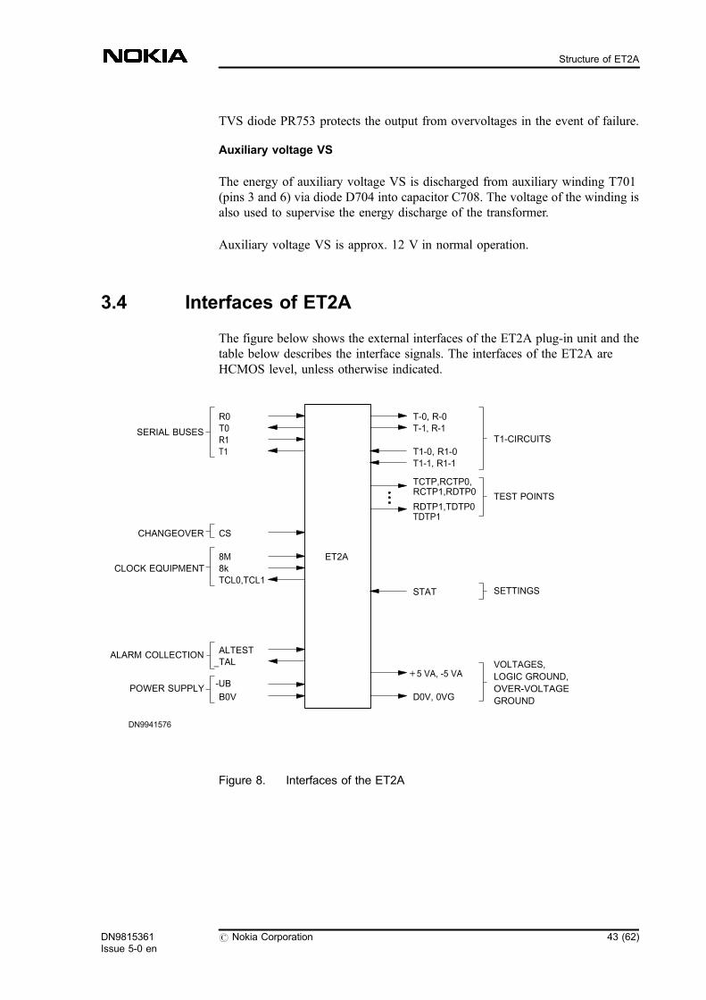
Figure 8. Interfaces of the ET2A 43
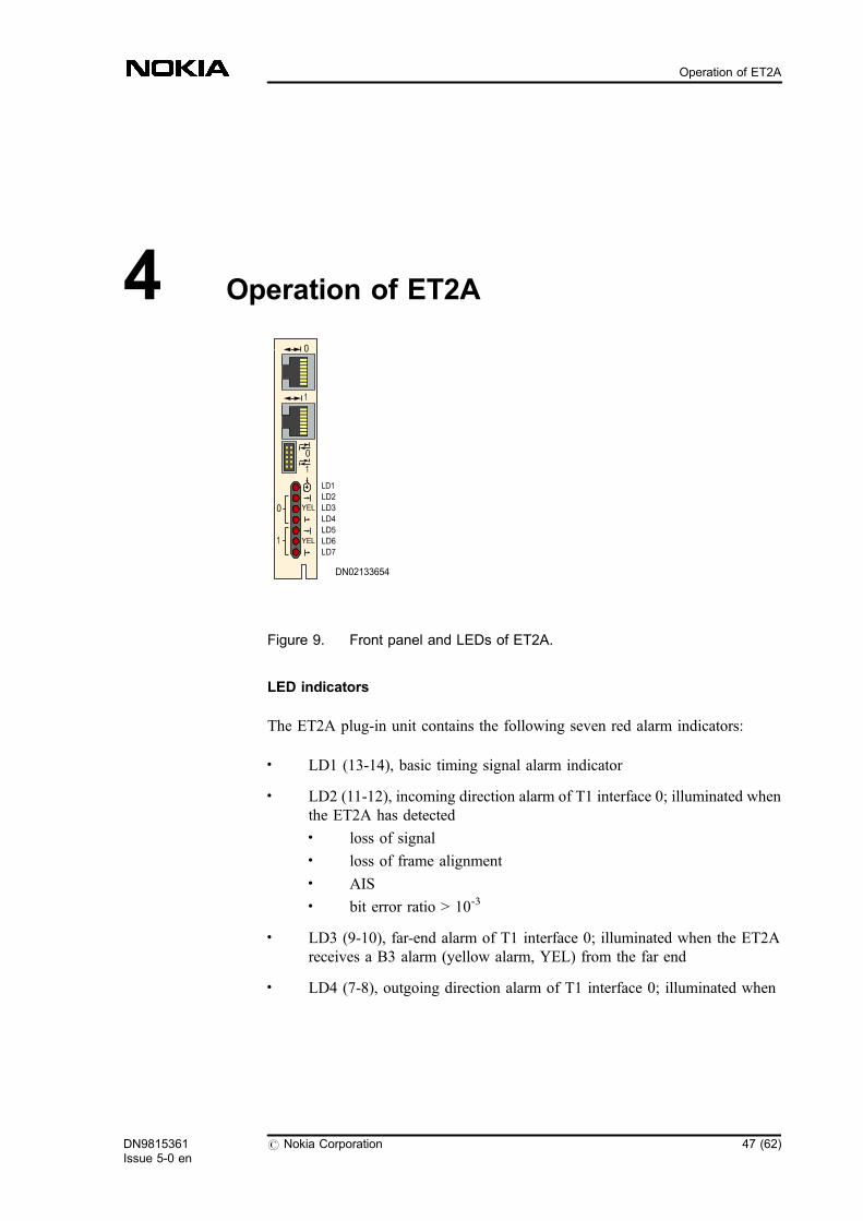
Figure 9. Front panel and LEDs of ET2A. 47
Figure 10. Jumper groups and EPROM circuits of plug-in unit ET2A 51
DN9815361Issue 5-0 en
# Nokia Corporation 5 (62)
List of figures

6 (62) # Nokia Corporation DN9815361Issue 5-0 en
ET2A

Summary of changes
Changes between document issues are cumulative. Therefore, the latest documentissue contains all changes made to previous issues.
Changes between issues 4-0 and 5-0
Structural changes. No effect on the contents of the document.
Changes between issues 3-0 and 4-0
Structure changed to NOM standard. Editorial changes.
Changes between issues 2-1 and 3-0
Chapter Jumpers, wirings and LED indicators modified, including figure ET2Aplug-in unit and table Standard settings. Connector maps moved to appendixConnector maps and table Map of connector P1 modified.
Changes between issues 2-0 and 2-1
No major changes, only minor errors corrected.
Changes for Issue 2
The section DC/DC converter in the Operation chapter has been made morespecific. Connector maps for the plug-in unit have been added to the chapterJumpers, wiring, LED indicators and connector maps.
DN9815361Issue 5-0 en
# Nokia Corporation 7 (62)
Summary of changes

8 (62) # Nokia Corporation DN9815361Issue 5-0 en
ET2A

1 ET2A overviewMain functions of ET2A in incoming transmission direction
The ET2A plug-in unit performs the following functions in the incomingtransmission direction:
. regenerates the 1.544 Mbit/s signal meeting the standard T1.403 andextracts the clock signal
. dissolves the line code (B8ZS or AMI)
. removes the jitter and compensates for the wander
. becomes synchronized with the SF or ESF frame meeting the standardT1.403
. supervises the bit errors with the CRC-6 and the frame alignment signal
. supervises the slips
. supervises the other interference on the line (loss of signal, AIS received,loss of frame alignment, CRC-6 multiframe alignment not achieved)
. supervises the far-end alarms
. lets time slots 1...24 through without changes
. sends the AIS towards the Switching Matrix in time slots 1...24 ascommanded by a message or due to interference in the incomingtransmission direction.
Main functions of ET2A in outgoing transmission direction
In the outgoing transmission direction, the ET2A plug-in unit performs thefollowing functions:
. generates an SF or ESF frame structure in accordance with standardT1.403 so that time slots T1...T24 are let through without changes
. send the AIS
DN9815361Issue 5-0 en
# Nokia Corporation 9 (62)
ET2A overview

. as commanded by a message or
. during an equipment loop or
. when the control connection has broken or
. if the basic timing signals are missing
. sends a far-end alarm as commanded by a message or due to interferencedetected in the incoming transmission
. converts the TTL level signal into the format required by the line code(AMI or B8ZS) and further into a three-level line signal
. attenuates the level of the output signal in increments of 0 dB, 7.5 dB,15 dB, 22.5 dB.
Operating environment of ET2A
The ET2A plug-in unit is used as the T1 trunk circuit interface in the Base StationController and Transcoder. The ET2A is connected to no more than two T1circuits. In the Base Station Controller, the ET2A is also connected to the GroupSwitch (GSW) and via it to the computer unit supervising the Exchange Terminal,to the Clock Equipment (CLO), to the general Hardware Alarm Collection Unit(HWAL) and to the power supply (see the figure below).
Figure 1. Operating environment of the ET2A in the Base Station Controller
POWER SUPPLY
CLO
HWAL
ET2A
BASIC TIMINGSIGNALS
T1-CIRCUIT 0
T1-CIRCUIT 1
GSW
MICROCOMPUTER UNITTHAT SUPERVISESAND CONTROLS THEEXCHANGE TERMINAL
WIRED ALARM
TEST CONTROL
OMUCHANGEOVER
SIGNAL
DN9941549
10 (62) # Nokia Corporation DN9815361Issue 5-0 en
ET2A

In the Transcoder, the ET2A is also connected to the TRCO plug-in unit and tothe power supply in addition to the T1 circuits (see the figure below)
Figure 2. Operating environment of the ET2A in the Transcoder
DN9941552
TRCO
ET2A
BASIC TIMINGSIGNALS
SERIALINTERFACES
T1-CIRCUIT 0
T1-CIRCUIT 1
DN9815361Issue 5-0 en
# Nokia Corporation 11 (62)
ET2A overview

12 (62) # Nokia Corporation DN9815361Issue 5-0 en
ET2A

2 Capacity and performance of ET2A
One ET2A can be connected to a maximum of two T1 circuits..
DN9815361Issue 5-0 en
# Nokia Corporation 13 (62)
Capacity and performance of ET2A

14 (62) # Nokia Corporation DN9815361Issue 5-0 en
ET2A

3 Structure of ET2A
3.1 Mechanical structure of ET2A
The ET2A plug-in unit has the dimensions 100 mm × 220 mm (height × depth).The ET2A is connected to the motherboard by one 3 × 32 -pin maleEuroconnector (P1). It is connected to the T1 circuits by two RJ48C-typeconnectors on the front panel (J2 and J3). The front panel of the ET2A alsocontains a test interface (J1) and seven red alarm indicators (LEDs). In addition,the ET2A plug-in units is equipped with a test interface (P2).
3.2 Logical structure of ET2A
The ET2A plug-in unit is composed of the following blocks (see the figurebelow):
. interface with Switching Matrix
. telecommunications circuit
. interface with Clock Equipment and timing
. changeover logic
. frame aligner 0 and 1
. line interface 0 and 1
. microcomputer
. DC/DC converter.
DN9815361Issue 5-0 en
# Nokia Corporation 15 (62)
Structure of ET2A
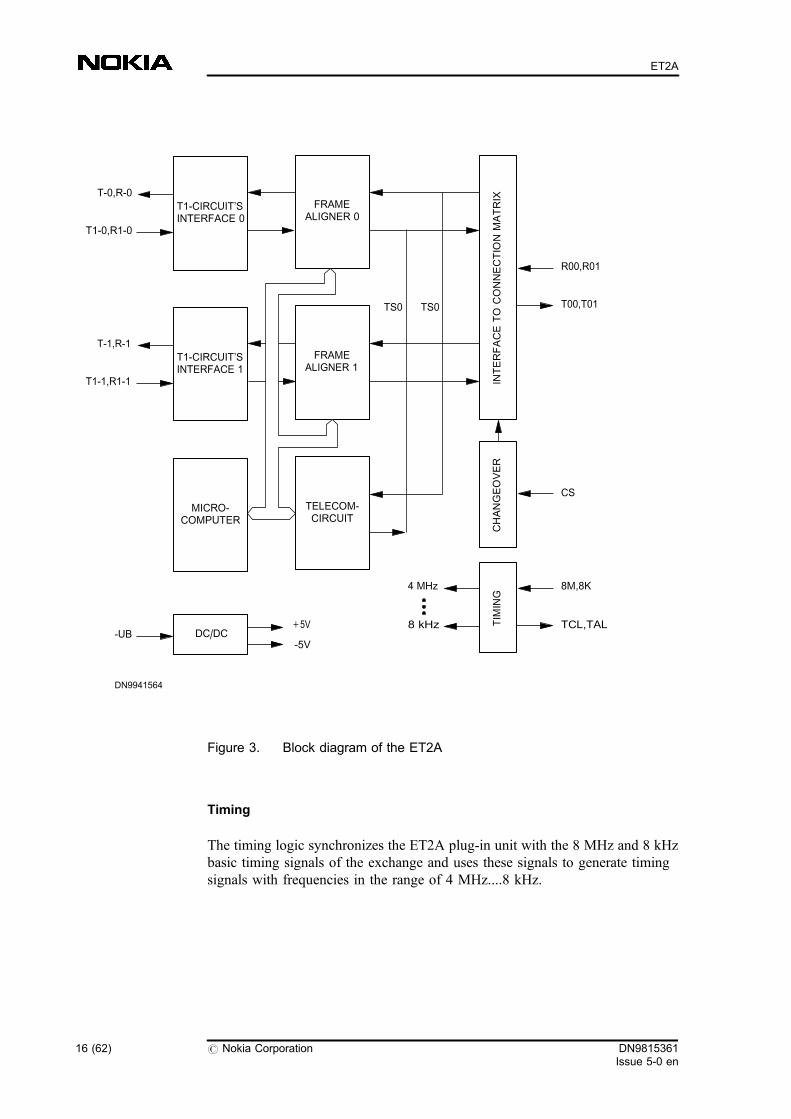
Figure 3. Block diagram of the ET2A
Timing
The timing logic synchronizes the ET2A plug-in unit with the 8 MHz and 8 kHzbasic timing signals of the exchange and uses these signals to generate timingsignals with frequencies in the range of 4 MHz....8 kHz.
R00,R01
T00,T01
CS
8M,8K
TCL,TAL
T-0,R-0
T-1,R-1
T1-1,R1-1
T1-0,R1-0
FRAMEALIGNER 0
FRAMEALIGNER 1
T1-CIRCUIT’SINTERFACE 1
MICRO-COMPUTER
INTERFACETOCONNECTIONMATRIX
CHANGEOVER
TS0 TS0
TELECOM-CIRCUIT
DC/DC-UB+5V
-5V
4 MHz
8 kHz
DN9941564
TIMING
T1-CIRCUIT’SINTERFACE 0
16 (62) # Nokia Corporation DN9815361Issue 5-0 en
ET2A

Microcomputer
The microcomputer of the ET2A plug-in unit controls and supervises theoperation of the other blocks in the ET2A. The microcomputer communicateswith the computer unit supervising the ET2A over an HDLC-based messagechannel which is transferred in time slot 0 of the PCM circuits connected to theSwitching Matrices. The microcomputer also controls the LEDs indicating thealarms of the T1 circuit interfaces of the ET2A.
The application program of the microcomputer (e.g. the T1 circuit supervisionprogram) is located in the random access memory of the ET2A. The program isloaded when needed via the message channel. The permanent sections of theprogram (e.g. the operating system and the loading program) are located in theread-only memory of the ET2A.
Incoming direction of T1 circuit
The T1 circuit interface regenerates the signal coming from the T1 circuit,extracts the 1.544 MHz timing signal from it by means of a phase lock andremoves any high-frequency jitter. The frame aligner dissolves the line code(B8ZS or AMI) of the T1 signal, finds the frame alignment signal in the T1 signaland becomes synchronized with it. If the operating mode has been chosen as ESF,the frame aligner will next find the CRC-6 multiframe alignment signal in the T1signal and become synchronized with it. If the operating mode has been chosen asSF, no synchronization with the multiframe will take place, and the T1 signal iswritten at the rate of the timing received from the T1 circuit into a receive bufferlocated in the frame aligner. From there, the signal is read at the rate of the timingof the exchange and transferred out of the frame aligner. A buffer memoryremoves low-frequency jitter and wander from the T1 signal. The wander is alsocompensated for when necessary by means of slips.
The 24 time slots of the T1 circuit are transferred via a serial interface to timeslots 1...24 of the PCM circuits connected to the Switching Matrices.
The ET2A plug-in unit supervises the interference on the T1 circuit and thealarms received from the far end, and counts the bit errors by means of the framealignment signal and the CRC-6 function.
Outgoing direction of T1 circuit
The serial bus interface of the ET2A plug-in unit transfers the PCM signalreceived from the active Switching Matrix to the frame aligner where time slots1...24 of the PCM signal are written at the rate of the timing of the exchange intothe output buffer. The time slots are read from the output buffer at the rate of the
DN9815361Issue 5-0 en
# Nokia Corporation 17 (62)
Structure of ET2A

timing of the T1 circuit which is generated from the basic timing signals of theexchange by means of a phase lock. At the same time, the frame aligner generatesthe frame alignment signal and the CRC-6 multiframe alignment signal if theoperating mode has been chosen as ESF.
When the T1 signal has been converted into the format required by the line code(AMI or B8ZS), it is sent to the T1 circuit via the line interface.
DC/DC converter
The operating voltages needed by the ET2A plug-in unit are generated by apower supply circuit integrated into the ET2A (DC/DC converter) from thebattery supply voltage (-UB).
3.3 Operating principles of ET2A
3.3.1 Timing
Line receiver IC3 receives the incoming 8.192 MHz and 8 kHz basic timingsignals from the Clock Equipment.
The timing signal block generates the timing signals needed by the other blocksby dividing the 8M basic timing signal in divider chain IC7, IC8 and IC9. Thesignal 8KD formed from the 8 kHz basic timing signal is used for the parallelloading of the divider chain.
The signals CLKB(9:0) obtained from the divider chain are used to generate theother timing signals needed by the ET2A plug-in unit. In addition, phase lockIC31 generates the clock signal 6176K (frequency 6.176 MHz) from the 2.048MHz clock signal _C2M. The 6176K signal is needed in the timing of the T1circuit.
The figure below shows the timing signals of the ET2A and the table belowdescribes the signals.
18 (62) # Nokia Corporation DN9815361Issue 5-0 en
ET2A

Figure 4. Timing signals of the ET2A
Table 1. Description of timing signals.
Signal Description
8M 8.192 MHz basic timing signal received from ClockEquipment
8K 8 kHz basic timing signal received from Clock Equipment
8KD Delayed 8 kHz synchronization signal
C4M,4MR 4.096 MHz timing signal
C2M, _C2M 2.048 MHz timing signal
B2B1R0/T0
IC106/2
IC15/9
IC123/2
RDO
IC124/2
IC3/4
8MT(NTIM=1)
8MT(NTIM=0)
4MR(NTIM=1
4MR(NTIM=0)
IC3/9
8KD
C4M
C2M
C4MD
_C2MD
C2MD
XBSYI
SLCKI
SLSYI
NEW FRAME BEGINS
DN9941588
DN9815361Issue 5-0 en
# Nokia Corporation 19 (62)
Structure of ET2A

Table 1. Description of timing signals. (cont.)
Signal Description
8MT 8.192 MHz timing signal
C4MD Delayed 4.096 MHz timing signal
6176K 6.176 MHz timing signal
C2MD, _C2MD Delayed 2.048 MHz timing signal
SYNC, SLSYI, XBSYI 8 kHz synchronization signal
3.3.2 Microcomputer
The processor of the microcomputer in the ET2A plug-in unit is IC14 (80C188)which has a 16-bit internal structure but an 8-bit external data bus. The clockfrequency of the microprocessor is 10 MHz which is generated by a crystaloscillator (XO1) operating at twice the frequency (20 MHz).
The read-only memory of the microcomputer is implemented with IC4 which is a256 kbyte EPROM. The EPROM contains the non-loadable parts of the ET2Aprogram (e.g. loading program). The memory circuit is addressed with the UCSselection signal of the processor.
The random access memory of the microcomputer in the ET2A is implementedwith IC5 which is a 512 kbyte pseudostatic RAM. The upper 256 kbyte area ofthe memory has been allocated as code area, and this area can be write-protectedwith an I/O command.
The processor of the ET2A handles the refreshment of the RAM circuit by itsrefresh automatics (_RFSH pin IC14/64). When the processor is reset, therefreshment handled by the processor ends. The RAM circuit is then set into self-fresh operating mode by keeping input 24 of the RAM circuit in state 0 and input22 in state 1. The contents of the RAM circuit will thus be retained during a reset.The RAM circuit is addressed with a signal formed from address bus signal AD(19) by port IC121.
The processor is reset when the _CPU_RESET signal is in state 0. Register circuitIC26 is reset at the same time, and the bottom six LED indicators on the frontpanel of the ET2A are illuminated.
The _CPU_RESET signal is activated in the following situations:
20 (62) # Nokia Corporation DN9815361Issue 5-0 en
ET2A
. when the +5 Voperating voltage is switched on; the reset pulse (approx. 2s) is formed with RC time constant R146 and C1
. under the control of the watchdog
. when pressing the reset switch on the Processor Test Adapter (PRTA).
When the +5 V operating voltages are switched on, the serial input/outputcontroller IC25 is reset via register circuit IC21.
Watchdog IC27 resets the processor, unless IC27 is reset at least every 60 ms. Theclock signal of IC27 is generated by an RC oscillator (IC126, R151 and C137).
The programmable timers of the processor are fed with a 1.25 MHz signal whichis generated by divider circuit IC27 from the 20 MHz clock signal provided byoscillator XO1.
The ET2A contains four write registers in the I/O address space of themicroprocessor (IC21, IC26, IC16 and IC17), which are used to control thefunctions of the ET2A and four read registers (IC19, IC20, IC22 and IC23),which are used to read the states of the status signals associated with theoperation of the ET2A.
The table below shows the memory address map of the ET2A.
Table 2. Memory address map of the ET2A.
Address area Memory
F0000H...FFFFFH EPROM
E0000H...EFFFFH EPROM
D0000H...DFFFFH EPROM
C0000H...CFFFFH EPROM
70000H...7FFFFH RAM *)
60000H...6FFFFH RAM *)
50000H...5FFFFH RAM *)
40000H...4FFFFH RAM *)
30000H...3FFFFH RAM
20000H...2FFFFH RAM
10000H...1FFFFH RAM
00000H...0FFFFH RAM
DN9815361Issue 5-0 en
# Nokia Corporation 21 (62)
Structure of ET2A

*) Memory area which can be write-protected
The table below shows the I/O address map of the ET2A.
Table 3. I/O address map of the ET2A.
I/O address area Signal Type Use
FF00H...FFFFH I/O 188 Control Block
9C00H...FEFFH Not used
9800H...9BFFH I I = status register 1
9400H...97FFH I Identification register
8400H...87FFH I/O HSCX
4000H...83FFH Not used
3800H...3FFFH O Not used
3000H...37FFH O Register indicating the attenuationof the incoming direction of circuit1
2800H...2FFFH O ET1 control register
2000H...27FFH I/O O = ET0 control register
1 = Register indicating theattenuation of the incomingdirection of circuit 0
1800H...1FFFH I/O T1 frame aligner circuit 1
1000H...17FFH I/O T1 frame aligner circuit 0
0800H...0FFFH O LED indicator register
0680H...07FFH _PCS5,_PSC6
Not used
0600H...067FH _PCS4 I/O PRTA
0580H...05FFH _PCS3 O I/O port 1, reset of HSCX circuitetc.
0480H...057FH _PCS1,_PSC2
Not used
0400H...047FH _PCS0 O Watchdog
0000H...03FFH Not used
ET0 = T1 circuit interface 0
22 (62) # Nokia Corporation DN9815361Issue 5-0 en
ET2A
ET1 = T1 circuit interface 1
The table below describes the bits in the write registers of the ET2A and Table 7describes the bits in the read registers of the ET2A.
Table 4. Write registers of the ET2A
Adress Bit Signal Description
0580H
(IC21)
0 _STOP_TR0 State 0: sending of T1 signal to circuit 0is disrupted
State 1: normal operation
1 _STOP_TR1 State 0: sending of T1 signal to circuit 1is disrupted
State 1: normal operation
2 PROTECT State 0: possible to write in the entireRAM area
State 1: the parts of the RAM which canbe protected are write-protected
3 _ALACK State 0: Acknowledges the alarm of thephase lock supervision circuit by settingthe signal _PLL_AL into state 1
State 1: normal operation
4 Not used
5 Not used
6 RES_HSCX State 0: normal operation
State 1: resets the HSCX circuit
7 Not used
0800H
(IC26)
0 LED1
(State 0 =
LED illuminated)
ET 0: Incoming direction alarm
Turned on when the following isdetected:
- loss of signal
- loss of frame alignment
- AIS
- bit error ratio > 10-3 .
1 LED2
(State 0 =
LED illuminated)
ET 0: Far-end alarm
Turned on when an alarm is receivedfrom the far end.
DN9815361Issue 5-0 en
# Nokia Corporation 23 (62)
Structure of ET2A

Table 4. Write registers of the ET2A (cont.)
Adress Bit Signal Description
2 LED3
(State 0 =
LED illuminated)
ET 0: Outgoing direction alarm
Turned on when:
- sending the AIS to the line
- equipment or line loop is engaged.
3 Not used.
4 LED4
(State 0 =
LED illuminated)
ET 1: Incoming direction alarm
Turned on when the following isdetected
- loss of signal
- loss of frame alignment
- AIS
- bit error ratio > 10-3 .
5 LED5
(State 0 =
LED illuminated)
ET 1: Far-end alarm
LED5
(State 0 =
LED illuminated)
Turned on when an alarm is receivedfrom the far end.
6 LED6
(State 0 =
LED illuminated)
ET 1: Outgoing direction alarm
Turned on when:
- sending the AIS to the line
- equipment or line loop is engaged.
7 Not used.
2000H
(IC16)
0 JASEL_0 State 0: Jitter attenuator in outputdirection
State 1: Jitter attenuator in inputdirection
Not used.
1 EGL_0 State 0: Attenuation tolerance 0...36 dB
State 1: Attenuation tolerance 0...26 dB
24 (62) # Nokia Corporation DN9815361Issue 5-0 en
ET2A
Table 4. Write registers of the ET2A (cont.)
Adress Bit Signal Description
2 LBO1_0 Outgoing direction signal attenuation:
LBO2 LBO1
0 0 0 dB
0 1 7.5 dB
1 0 15 dB
1 1 22.5 dB
3 LBO2_0 See LBO1_0
4 RLOOP_0 State 0: Normal operation
State 1: Line loop
IC33 is reset by setting RLOOP andLLOOP into state 1 and TAOS into state0.
5 LLOOP_0 State 0: Normal operation
State 1: Equipment loop
6 TAOS_0 State 0: Normal operation
State 1: Sending of AIS to line
7 TCLE_0 State 0: Synchronization signal TCLOgoing to Clock Equipment is disrupted.
State 1: Normal operation
2800H
(IC17)
0 JASEL_1 State 0: Jitter attenuator in outputdirection
State 1: Jitter attenuator in inputdirection
Not used.
1 EGL_1 State 0: Attenuation tolerance ofincoming direction signal is 0...36 dB
State 1: Attenuation tolerance ofincoming direction signal is 0...26 dB
2 LBO1_1 Attenuation of outgoing direction signal:
LBO2 LBO1
0 0 0 dB
0 1 7.5 dB
1 0 15 dB
1 1 22.5 dB
3 LBO2_1 See LBO1_1
DN9815361Issue 5-0 en
# Nokia Corporation 25 (62)
Structure of ET2A
Table 4. Write registers of the ET2A (cont.)
Adress Bit Signal Description
4 RLOOP_1 State 0: Normal operation
State 1: Line loop
IC32 is reset by setting RLOOP andLLOOP into state 1 and TAOS into state0.
5 LLOOP_1 State 0: Normal operation
State 1: Equipment loop
6 TAOS_1 State 0: Normal operation
State 1: Sending of AIS to line
7 TCLE_1 State 0: Synchronization signal TCL1going to Clock Equipment is disrupted.
State 1: normal operation
Table 5. Read registers of the ET2A.
Address Bit Signal Description
2000H
(IC23)
0 LATN1_0 LATN1_0...LATN5_0
Attenuation level of incoming directionsignal to T1 circuit interface 0:
4 ones 0...7.5 dB
1 one 7.5...15 dB
2 ones 15...22.5 dB
3 ones more than 22.5 dB
1 LATN2_0 See LATN_1_0
2 LATN3_0 See LATN_1_0
3 LATN4_0 See LATN_1_0
4 LATN5_0 See LATN_1_0
5 Not used
6 Not used
7 Not used
26 (62) # Nokia Corporation DN9815361Issue 5-0 en
ET2A

Table 5. Read registers of the ET2A. (cont.)
Address Bit Signal Description
3000H
(IC22)
0 LATN1_1 LATN1_1...LATN5_1
Attenuation level of incoming directionsignal to T1 circuit interface 1:
4 ones 0...7.5 dB
1 one 7.5...15 dB
2 ones 15...22.5 dB
3 ones more than 22.5 dB
1 LATN2_1 See LATN_1_1
2 LATN3_1 See LATN_1_1
3 LATN4_1 See LATN_1_1
4 LATN5_1 See LATN_1_1
5 Not used
6 Not used
7 Not used
9400H
(IC37)
0 CHA0 Interchangeability (least significant bit):jumper
1 CHA1 Interchangeability (most significant bit):jumper
2 TYP0 Type information (least significant bit)
3 TYP1 Type information
4 TYP2 Type information
5 TYP3 Type information
6 TYP4 Type information
7 TYP5 Type information (most significant bit)
9800H 0 LOS_0 IC33 status signal LOS
0: No interference
1: Loss of incoming signal
1 NLOOP_0 IC33 status signal NLOOP
0: Normal operating state
1: Bit pattern 00001 received for 5 s fromthe far end and network loopbackactivated
DN9815361Issue 5-0 en
# Nokia Corporation 27 (62)
Structure of ET2A
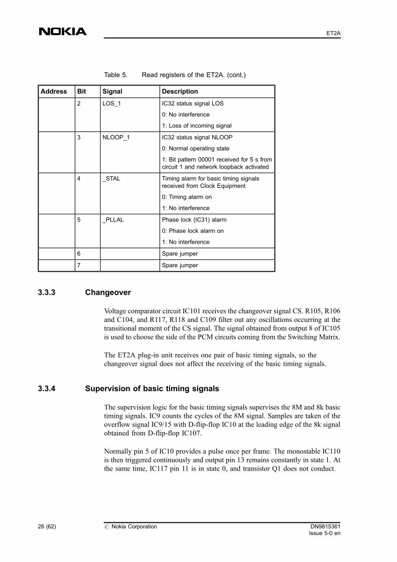
Table 5. Read registers of the ET2A. (cont.)
Address Bit Signal Description
2 LOS_1 IC32 status signal LOS
0: No interference
1: Loss of incoming signal
3 NLOOP_1 IC32 status signal NLOOP
0: Normal operating state
1: Bit pattern 00001 received for 5 s fromcircuit 1 and network loopback activated
4 _STAL Timing alarm for basic timing signalsreceived from Clock Equipment
0: Timing alarm on
1: No interference
5 _PLLAL Phase lock (IC31) alarm
0: Phase lock alarm on
1: No interference
6 Spare jumper
7 Spare jumper
3.3.3 Changeover
Voltage comparator circuit IC101 receives the changeover signal CS. R105, R106and C104, and R117, R118 and C109 filter out any oscillations occurring at thetransitional moment of the CS signal. The signal obtained from output 8 of IC105is used to choose the side of the PCM circuits coming from the Switching Matrix.
The ET2A plug-in unit receives one pair of basic timing signals, so thechangeover signal does not affect the receiving of the basic timing signals.
3.3.4 Supervision of basic timing signals
The supervision logic for the basic timing signals supervises the 8M and 8k basictiming signals. IC9 counts the cycles of the 8M signal. Samples are taken of theoverflow signal IC9/15 with D-flip-flop IC10 at the leading edge of the 8k signalobtained from D-flip-flop IC107.
Normally pin 5 of IC10 provides a pulse once per frame. The monostable IC110is then triggered continuously and output pin 13 remains constantly in state 1. Atthe same time, IC117 pin 11 is in state 0, and transistor Q1 does not conduct.
28 (62) # Nokia Corporation DN9815361Issue 5-0 en
ET2A
If interference occurs in the basic timing signals, IC110 will not be triggered oftenenough, and output pin 13 has time to drop to state 0, and IC110 pin 5 provides apulse with a minimum duration of 50 ms. This turns on alarm indicator LD1 andtransistor Q1 enters conducting state which in turn activates alarm signal _TAL.
The alarm output can be tested with the logic-level test signal ALTST. State 1 ofthis signal causes an alarm and state 0 enables normal operation. The LEDindicator is not illuminated during a test alarm.
3.3.5 Incoming direction
Regeneration of PCM signal and extraction of timing
The incoming transmission direction of the T1 circuit is connected to the ET2Aplug-in unit via transformers T4 (interface 0) and T2 (interface 1). Resistors R181(interface 0) and R185 (interface 1) implement an input impedance of 100 Ωvisible to the circuit.
R154, R157, R203, R204, PR4, PR8, PR9 and F1 (interface 0) and R173, R209,R210, R211, PR2, PR6, PR11 and F3 (interface 1) protect the interfaces fromovervoltages and overcurrents. Gas discharge tubes PR9 and PR11 protect theinput interfaces from various types of overvoltages by short-circuiting inputs T1-0 and R1-0 and T1-1 and R1-1 when the voltage between the targets of the gasdischarge tube exceeds the ignition voltage. Since the gas discharge tubes areslow and only ignite at high voltages, the interfaces are also protected bysemiconductor protectors PR4 and PR8, and PR2 and PR6 which are fast andoperate at low voltages. Fuses F1 and F3 protect transformers T4 and T2 fromovercurrents.
The T1 signal is taken to T1 interface circuit IC33 (interface 0) and IC32(interface 1) which regenerates the signal which contains interference and hasbeen attenuated and converts it into two logic-level signals (IC33 and IC32 pins 6and 7). The T1 interface circuits IC33 and IC32 extract the 1.544 MHz timingsignal from the incoming signal (IC33 and IC32 pin 8) by means of an internalphase lock.
Two 8 kHz synchronization signals (TCL0 and TCL1) can be taken from theET2A to the synchronization unit. The synchronization signals are normallyseparated by frame alignment circuits IC29 (interface 0) and IC28 (interface 1).The frame alignment circuit provides a pulse-type 8 kHz synchronization signalat the frame bit of the incoming T1 circuit signal. The synchronization signal isobtained from pin RFSYO of the frame alignment circuit, and it is taken via portsIC102 to line transmitter circuit IC103 which converts the logic-levelsynchronization signals into differential format. The amplitude of signals TCL0A,TCL0B and TCL1A, TCL1B is limited by resistors to 0.4 V.
DN9815361Issue 5-0 en
# Nokia Corporation 29 (62)
Structure of ET2A

The microcomputer of the ET2A cuts off the TCL0 and TCL1 synchronizationsignal under various fault conditions on the incoming T1 circuit. The cut-off iscontrolled by signals TCLE_0 and TCLE_1 provided by register circuits IC16and IC17.
Decoding of line code and frame alignment
The frame aligner IC29 (interface 0) and IC28 (interface 1) dissolves the B8ZS orAMI line code of the regenerated input signal (IC29 and IC28 pins RNEGI andRPOSI) and becomes synchonized with the SF or ESF frame.
The frame alignment is considered lost when two out of four received framealignment bits have been faulty. The frame alignment is restored when the framealigner has found the frame alignment signal. In ESF mode, the frame aligner alsochecks the correctness of the CRC sum. If it finds several possible framealignment signals, if chooses the first frame alignment signal whose CRC sum isOK. In SF mode, the frame alignment takes an average of 5 ms, in ESF mode 10ms.
Supervision of T1 circuit
When frame alignment has been achieved, the microcomputer of the ET2A plug-in unit begins to supervise the state of the incoming T1 circuits by means of theframe alignment circuits. In SF mode, it monitors the following properties:
. breakages on the line
. AIS
. frame alignment
. bit errors by means of the frame alignment signal
. far-end alarm
. slips.
In ESF mode, it monitors the following properties:
. breaks on the line
. AIS
. frame alignment
. bit errors by means of the frame alignment signal and the CRC-6
. far-end alarm
30 (62) # Nokia Corporation DN9815361Issue 5-0 en
ET2A

. maintenance messages of the circuit conveyed over the data channel of theESF frame
. slips.
If the ET2A detects a disturbance in the PCM signal of the incoming direction, itacts according to the table below.
Table 6. Operation of the ET2A during disturbances on the T1 circuit.
Disturbance Sending ofAIS toSwitchingMatrix
Sending ofalarm to farend
Cutoff ofTCL
Alarm tocomputersupervisingPCM circuit
Loss ofincoming signal
Yes Yes Yes Yes
AIS received Yes Yes Yes Yes
Loss of framealignment
Yes Yes Yes Yes
Error ratio toohigh
Yes Yes Yes Yes
Alarm receivedfrom far end
No No No No
The T1 interface circuits IC33 and IC32 supervise the incoming signal. Thecircuits indicate a loss of incoming signal to the microcomputer of the ET2Awiththe signal LOS. The microcomputer can read the alarm from register circuit IC19.
The T1 interface circuits supervise the level of the incoming signal. Theygenerate the signal LATN where the number of 1s in five bits indicates the levelof the input signal. The LATN signal is converted into parallel format by shiftregisters IC23 (circuit 0) and IC22 (circuit 1), and can be read from these shiftregisters by the microcomputer of the ET2A.
Sending the PCM signal to the serial interface
The PCM signal RDO_0, RDO_1 of the incoming direction is obtained on logiclevel from pin 55 of synchronization circuits IC29 (interface 0) and IC28(interface 1). The data signals are taken to selector circuit IC124 where themaintenance LAPD channel generated by IC25 is directed to time slot 0 of circuit0. The data signals are taken out of IC124 at the leadsing edge of clock signalC2M. Then the 2.048 Mbit/s data signals are combined into one 4.096 Mbit/sdata signal in selector circuit IC125 by multiplexing them under the control of
DN9815361Issue 5-0 en
# Nokia Corporation 31 (62)
Structure of ET2A
clock signal _C2M. The 4.096 Mbit/s data signal is transferred from IC125 at theleading edge of clock signal C4MD (NTIM = 1) or C4M (NTIM = 0) to D-flip-flop IC12 where the data signal is timed to the nominal timing of the exchangewith clock signal 8MT.
The timing of the interface can be advanced by 61 ns by connecting the controlsignal NTIM going to the rear connector to state 0. By using the transmissionadvancement, the permitted length of the PCM circuit between the SwitchingMatrix and the ET2A plug-in unit can be increased.
From pin 5 of IC12, the data signal is taken to line transmitter circuit IC2. Fromthe line transmitter circuit, the data are switched to both sides of the SwitchingMatrix from interfaces T0A, T0B and T1A, T1B. The termination resistors of theinterfaces are located in the ET2A.
3.3.6 Outgoing direction
Line receiver IC1 receives the PCM signals (R0, R1) coming from both sides ofthe serial bus interface (Switching Matrix). The signals are taken to multiplexerregister circuit IC106 which is timed with timing signal 4MR. The delaying of thereception increases the permitted maximum length of the PCM circuit betweenthe Switching Matrix and ET2A plug-in unit.
The even and odd PCM circuit of the 4 Mbit/s serial interface are separated intotwo 2 Mbit/s data signals by flip-flop circuit IC15 and register circuit IC123. Theeven PCM circuit is used to form the data signal XDI_0 of interface 0 in theoutgoing direction and the odd PCM circuit is used to form the data signal XDI_1of interface 1.
Frame aligner IC29 receives data signal XDI_0 and frame aligner IC28 receivesdata signal XDI_1. The frame aligners generate a frame structure in accordancewith the standard ANSI T1.403 and encode the T1 signal in accordance with linecode AMI or B8ZS. Time slots 1...24 pass through the frame aligner without anychanges to their contents.
The output direction signals generated by frame aligners IC29 and IC28 aretransferred to the T1 circuit interfaces in signals XPOSO and XNEGO. TheXPOSO signal transfers the positive pulses to be sent to the T1 circuit and theXNEGO signal transfers the negative pulses. When both XPOSO and XNEGOare in state 0, 0 is sent to the circuit. The signals are connected at the circuitinterfaces to the transmitter section of the T1 interface circuits IC33 and IC32.Output pins TTIP and TRING of these circuits control transmission transformersT3 (interface 0) and T1 (interface 1) of the T1 interfaces. Resistors R175, R176,R182, R183 (interface 0) and R178, R179, R187, R188 (interface 1) adapt theamplitude of the signal to the level required by the standard.
32 (62) # Nokia Corporation DN9815361Issue 5-0 en
ET2A

R205, R206, R207, R208, PR3, PR7, PR10 and F2 (interface 0) and R212, R213,R214, R215, PR1, PR5, PR12 and F4 (interface 1) protect the interfaces fromovervoltages and overcurrents. Gas discharge tubes PR10 and PR12 protect theoutput interfaces from various types of overvoltages by short-circuiting outputs T-0 and R-0, and T-1 and R-1 when the voltage between the targets of the gasdischarge tubes exceeds the ignition voltage. Since the gas discharge tubes areslow and only ignite with high voltages, the interfaces are also equipped withsemiconductor protectors PR3 and PR7, and PR1 and PR5 which are fast andoperate with low voltages. Fuses F2 and F4 protect transformers T3 and T1 fromovercurrents.
The microcomputer of the ET2A can direct T1 interface circuits IC33 and IC32 tosend the AIS to the T1 circuit by means of the TAOS control signal of theinterface circuits. The microcomputer of the ET2A controls the TAOS signal viaregister circuits IC16 and IC17.
3.3.7 Loops
The microcomputer of the ET2A plug-in unit can loop the T1 circuit in the waysindicated in the figure below.
Figure 5. Loop options in the ET2A
In the line loop (loops 1 and 2), the incoming direction signal on the T1 circuit islooped to the outgoing direction circuit. The microcomputer of the ET2A canengage the line loop by setting control signal RLOOP_0 or RLOOP_1 into state1.
DN9941591
LINE INTERFACE 0
LINE INTERFACE 1
FRAME ALIGNER 0
FRAME ALIGNER1
SERIALBUSINTERFACE
T1-CIRCUIT 0
T1-CIRCUIT 1
1 3
2 4
5 7
6 8
R0, R1
T0, T1
DN9815361Issue 5-0 en
# Nokia Corporation 33 (62)
Structure of ET2A
In the equipment loop (loops 3 and 4), the data received from serial bus interfaceR0 and R1 are looped to outgoing serial bus interface T0 or T1. The AIS can thenbe sent to the T1 circuit. The microcomputer of the ET2A can engage theequipment loop by setting control signal LLOOP_0 or LLOOP_1 of the T1interface circuit into state 1. It can start the sending of the AIS by setting controlsignal TAOS_0 or TAOS_1 of the T1 interface circuit into state 1.
In the payload signal line loop (loops 5 and 6), time slots 1...24 in the incomingdirection of the T1 circuit are looped to the outgoing direction circuit. The framealignment signal is not looped. Instead, the frame aligner generates a new framealignment signal. The microcomputer of the ET2A can engage the payload signalline loop by setting the internal control signal `Enable Payload Loopback' of theframe aligner into state 1.
In the channel-specific loop (loops 7 and 8), the time slots (one or more) receivedfrom serial bus interface R0 and R1 are looped to outgoing serial bus interface T0and T1. The microcomputer of the ET2A can engage the channel-specific loop bysetting the internal control signal `Loop Transmit Input Channel' of the framealigner into state 1.
3.3.8 Maintenance interface
The ET2A plug-in unit is connected to the controlling and supervising computerunit by an HDLC-based message channel. The message channel uses time slot T0of the even PCM circuit of serial bus interface R, T.
In the input direction, the data signals obtained from line receiver circuit IC1connected to serial interface R0 and R1 are taken to selector circuit IC106. Theselector circuit provides the data signal of the 4 Mbit/s serial bus under the controlof the changeover signal IC105/8. This data signal is demultiplexed into two 2Mbit/s data signals by D-flip-flop IC15 and register circuit IC123.
The 2 Mbit/s data signal XDI_0 provided by the selector circuit is taken to HDLCcircuit (HSCX) IC25. HSCX circuit IC25 is timed with signals C2M and SYNC.The microcomputer of the ET2A chooses the maintenance time slot to be used bywriting it into the register of the HDLC circuit.
In the output direction, the data signal TXDB obtained from the HSCX circuit istaken to selector circuit IC124. HSCX circuit IC25 controls the selector circuitwith the signal TxCLKB which is activated for the duration of time slot T0. Pin 2of selector circuit IC124 then provides the signal going to the even PCM circuitof the serial bus interface where time slot T0 contains the data signal sent by theHSCX circuit. The signal is taken via register circuit IC125 and D-flip-flop IC12to line transmitter IC2.
34 (62) # Nokia Corporation DN9815361Issue 5-0 en
ET2A

3.3.9 DC/DC converter
3.3.9.1 Introduction to DC/DC converter
The figure below illustrates the principle of operation of the DC/DC converter.
DN9815361Issue 5-0 en
# Nokia Corporation 35 (62)
Structure of ET2A
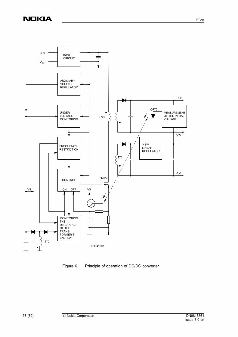
Figure 6. Principle of operation of DC/DC converter
INPUTCIRCUIT
AUXILIARYVOLTAGEREGULATOR
UNDER-VOLTAGEMONITORING
FREQUENCYRESTRICTION
MONITORINGTHEDISCHARGEOF THETRANS-FORMER’SENERGY
CONTROL
ON OFF
MEASUREMENTOF THE INITIALVOLTAGE
VSVS
+ 5 VLINEARREGULATOR
B0V
- U B
T701
T701
OP701
T701
+5 V
D0V
-5 V
Q705
DN9941607
36 (62) # Nokia Corporation DN9815361Issue 5-0 en
ET2A

The DC/DC converter is a current mode regulated flyback converter operating ana constant frequency of approx. 100 kHz. The operation takes place in full energytransfer mode.
Flyback transformer T701 stores energy in the air gap of its ferrite core whenMOSFET switch Q705 is conducting. When the primary current has been cut off,the polarities of the voltages across the windings are reversed, and the energy isdischarged from the secondary windings into filtering capacitors via diodes. Anew switching cycle does not begin until all energy has been discharged from thetransformer.
To regulate the output voltages, the voltage of the +5 V output is measured, andbased on the voltage the cut-off level of the primary current is changed viaoptoisolator OP701, which in turn changes the conducting time of MOSFETswitch Q705 (pulse width modulation). The voltage at the 5 Voutput is also post-regulated with a linear regulator.
3.3.9.2 Input circuit
Polarity and transient protection of input voltage
Serial diode D701 protects the converter if the polarity of the input voltage isincorrect.
Varistor VR701 and TVS diode PR751 protect the converter from transients inthe input voltage.
Overcurrent protection
Surface-mounted fuse F701 provides overcurrent protection for the converter inthe event of internal short-circuit failure.
Switching current protection
When the ET2A plug-in unit is connected to a connector in a cartridge with thevoltages on, the charging current of the input capacitors of the converter must belimited to protect the connector and fuse. Resistor R757 limits the chargingcurrent. When the voltage across the input capacitors has risen enough, resistorR757 is bypassed by the channel resistance of MOSFET Q702 before theconverter starts.
Interference filtering
The interference filtering is bidirectional. The interference caused by theconverter must not be switched back via the supply wires of the input voltage toother pieces of equipment, nor must the interference coming via the supplydisturb the operation of the converter.
DN9815361Issue 5-0 en
# Nokia Corporation 37 (62)
Structure of ET2A
The input filter is composed of Y-capacitors C751 and C752 connected from thesupply wires to ground, common mode coil L701, serial coil L702 and capacitorsC703...C705, C709, C710 and C712.
3.3.9.3 Auxiliary voltage regulator
The auxiliary voltage regulator decreases the voltage VS needed by the regulatorcircuit from the input voltage when the converter is started.
The regulator consists of zener diode Z702, transistor Q704 and resistors R759and R752. The regulator provides the voltage VS of approx. 9 V.
When the converter and the regulation of output voltages have started, the voltageobtained from the auxiliary winding (pins 3 and 6) of transformer T701 raises VSto approx. 12 V, and transistor Q704 is closed. The regulation circuit thus receivesall necessary power via the transformer, and the efficiency improves incontinuous state.
The auxiliary voltage regulator also powers the regulation circuit if the +5 Voutput of the converter is short-circuited, in which case the voltage obtained fromthe auxiliary winding drops.
3.3.9.4 Undervoltage supervision
The undervoltage supervision monitors the battery voltage and the auxiliaryvoltage of the regulation circuit. The battery voltage is supervised to prevent theconverter from draining the batteries of the exchange too much e.g. during apower outage, and to disable the operation of the converter when the inputvoltage is too low, making it impossible to regulate the output voltages. Thesupervision of the auxiliary voltage of the regulation circuit prevents theconverter from starting if the auxiliary voltage is too low, since the circuits wouldthen operate incorrectly.
Comparator circuit IC703 (pins 1, 6 and 7) monitors the low limit of the batteryvoltage. The voltage provided by resistor division R751 and R754 is comparedwith a 2.5 V reference generated by IC704. The output of the circuit remains instate 0 until the input voltage is high enough. R753 adds hysteresis to theoperation to prevent oscillation of the supervision at the voltage limit.
Comparator circuit IC703 (pins 2, 4 and 5) monitors the low limit of auxiliaryvoltage VS of the regulation circuit. The voltage provided by resistor divisionR769 and R761 is compared with a 2.5 V reference. The output of the circuitremains in state 0 until the auxiliary voltage is high enough. R773 adds hysteresisto the operation to prevent oscillation of the supervision at the voltage limit.
38 (62) # Nokia Corporation DN9815361Issue 5-0 en
ET2A

The outputs of both supervision circuits have been joined together (open-collectoroutputs), allowing the output signal to rise to state 1 only when permitted by bothsupervision circuits.
3.3.9.5 Frequency limitation
Timer circuit IC702 generates a monostable pulse whose duration determines thenormal operating frequency of the converter (approx. 100 kHz). R762 and C757determine the duration of the pulse. The undervoltage supervision circuits preventthe circuit from operating by keeping pin 4 in state 0 until the auxiliary voltageVS is high enough.
A pulse is always triggered when a new switching cycle begins in the converter, i.e. when pin 14 of comparator circuit IC703 enters state 0. The pulse obtainedfrom pin 3 of IC702 directs IC703 pin 14 into state 1 right away (via diode D705and resistor R760), preventing a new switching cycle from beginning while thepulse is active.
3.3.9.6 Supervision of transformer energy discharge
The supervision of the energy discharge also participates in preventing thebeginning of a new switching cycle in the converter before the energy of theprevious switching cycle has been discharged from transformer T701. Thesupervision prevents the transformer from being saturated and makes sure that theoperation will always take place in the desired full energy transfer mode (alsowhen the output voltage is short-circuited) which is easier to keep stable withregard to the regulation.
When all the energy has been discharged from the transformer, the voltagesacross the windings disappear. This change is also visible in auxiliary windingT701 (pins 3 and 6). The supervision takes place by measuring the voltage of theauxiliary winding in the transformer. The voltage to be measured is filtered byresistors R763 and R772 and capacitor C762. The voltage is added via diodeD705 to the same resistor (R760) as the frequency limitation pulse. Themeasurement reference at IC703 pin 8 is approx. 0.25 V. IC703 pin 14 enters state0 only when the voltage at resistor R760 has dropped below the reference,allowing a new switching cycle to begin. The measurement reference is this lowso that the supervision will also operate when the output voltage of the converteris short-circuited, in which case only the threshold voltage of the diode is actingacross the output winding. The energy discharge from the transformer will thentake longer, since the voltage into which the energy is discharged is low. Theoperating frequency of the converter will thus drop during a short circuit.
DN9815361Issue 5-0 en
# Nokia Corporation 39 (62)
Structure of ET2A
3.3.9.7 Control
Timer circuit IC701 acting as an RS flip-flop controls MOSFET switch Q705directly. The undervoltage supervision circuits prevent the circuit from operatingby keeping pin 4 in state 0 until the auxiliary voltage VS is high enough.
ON control
The ON control is activated by directing IC701 pin 2 for a while into state 0 withthe output of comparator circuit IC703 (pin 14), causing the output of IC701 (pin3) to direct MOSFET switch Q705 closed. Q705 remains closed until an OFFcontrol is received.
OFF control
The OFF control is based on the measurement of the primary current oftransformer T701. A voltage proportional to the primary current is obtainedacross resistors R766; R777...R779, R786 when MOSFET switch Q705 is closed.The switching spike of the current is filtered out of the voltage with RC circuitR768 and C761. The current measurement signal is taken to one input ofcomparator circuit IC701 (pin 10). The reference voltage (approx. 0.25 V) isconnected to the other input (pin 11). When the value of the current measurementvoltage exceeds the reference, the output of comparator circuit IC703 (pin 13)enters state 0 and directs IC701 pin 6 into state 1 by means of transistor Q703,causing the output of the circuit (pin 3) to enter state 0, and MOSFET switchQ705 opens.
The OFF control signal is also added by means of diode D703 to resistor R760,which prevents the ON control from being activated as long as the OFF control isactive, because the control of pin 2 of timer circuit IC701 has higher priority thanthe control of pin 6.
When the primary current has been cut off and the measurement currentdisappears, the output of comparator circuit IC703 (pin 13) returns to state 1.
The current-mode regulation is implemented by adding a DC current to resistorR768 by means of optoisolator OP701 which primarily depends on the load onthe +5 V output. When the load on the converter is low, a larger DC current isadded to the resistor, and MOSFET switch Q705 is directed open with a smallerprimary current value (the control pulse of Q705 becomes narrower), and theamount of energy to be transferred in the switching cycle decreases. Theregulation principle is thus current mode pulse width modulation (PWM).
3.3.9.8 Operation of primary circuit
The figure below illustrates the operation of the primary circuit.
40 (62) # Nokia Corporation DN9815361Issue 5-0 en
ET2A
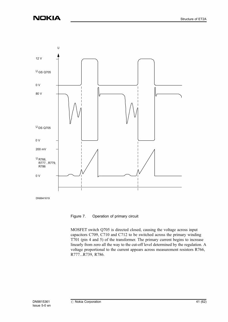
Figure 7. Operation of primary circuit
MOSFET switch Q705 is directed closed, causing the voltage across inputcapacitors C709, C710 and C712 to be switched across the primary windingT701 (pin 4 and 5) of the transformer. The primary current begins to increaselinearly from zero all the way to the cut-off level determined by the regulation. Avoltage proportional to the current appears across measurement resistors R766,R777...R739, R786.
U
200 mV
0 V
U DS Q705
80 V
0 V
0 V
U R766,R777...R779,R786
12 V
U GS Q705
DN9941619
DN9815361Issue 5-0 en
# Nokia Corporation 41 (62)
Structure of ET2A
The primary pulse current is taken from the input capacitors which will contain aripple voltage. The interference filtering of the input circuit strives to filter theinput voltage towards the battery so that only a DC current is drawn from thebattery voltage.
When Q705 is directed open, the leakage parameters of the components willcause a voltage spike across Q705 and oscillation which is attenuated withsnubber connection C714, R774 and R785.
3.3.9.9 Operation of secondary circuits
When Q705 is directed open, the voltages across the windings of transformerT701 are reversed, and the energy stored in the air gap of the ferrite core of thetransformer is discharged from the secondary windings through the diodes intothe output capacitors.
+5 V output
The energy of the +5 Voutput is discharged from secondary winding T701 (pins1 and 8) via diode SD702 into capacitors C724 and C728. The ripple voltagecaused by the pulse current is attenuated by LC circuit L703 and C723. CapacitorC765 returns the interference coupled through the transformer to the primary side.
The output voltages of the converter are regulated by measuring the voltage at the+5 Voutput. The measurement is conducted with parallel regulator circuit IC705which contains a differential amplifier and a 2.5 V reference. The measurementinformation is transferred to the current measurement circuit on the primary sideby means of optoisolator OP701, because the primary and secondary sides of theconverter are galvanically separated from each other.
The short-circuit current of the output is limited by the supervision of the energydischarge of the transformer by dropping the operating frequency.
TVS diode PR752 protects the output from overvoltages in the event of failure.
-5 V output
The energy from the -5 Voutput is discharged from winding T701 (pins 2 and 7)via diode SD701 into capacitor C727. Zener diode Z703 protects the capacitorfrom overvoltages if the -5 Voutput is loaded very lightly (the voltage may rise ifthe +5 V output is loaded heavily at the same time, since it determines theregulation).
Additional regulation of the -5 Voutput is performed with linear regulator IC751.Additional regulation is needed, because the -5 Voutput is loaded less than the +5Voutput which determines the regulation (both outputs are implemented with thesame transformer). The regulator also limits the short-circuit current of the output.
42 (62) # Nokia Corporation DN9815361Issue 5-0 en
ET2A
TVS diode PR753 protects the output from overvoltages in the event of failure.
Auxiliary voltage VS
The energy of auxiliary voltage VS is discharged from auxiliary winding T701(pins 3 and 6) via diode D704 into capacitor C708. The voltage of the winding isalso used to supervise the energy discharge of the transformer.
Auxiliary voltage VS is approx. 12 V in normal operation.
3.4 Interfaces of ET2A
The figure below shows the external interfaces of the ET2A plug-in unit and thetable below describes the interface signals. The interfaces of the ET2A areHCMOS level, unless otherwise indicated.
Figure 8. Interfaces of the ET2A
ET2A
T-0, R-0R0
T-1, R-1T0
R1
T1-0, R1-0T1
T1-1, R1-1
CS
8M
8k
TCL0,TCL1
STAT
ALTEST
_TAL
+5 VA, -5 VA
D0V, 0VGB0V
TCTP,RCTP0,RCTP1,RDTP0
RDTP1,TDTP0TDTP1
T1-CIRCUITS
TEST POINTS
SETTINGS
VOLTAGES,
LOGIC GROUND,
OVER-VOLTAGE
GROUND
SERIAL BUSES
CHANGEOVER
CLOCK EQUIPMENT
POWER SUPPLY-UB
ALARM COLLECTION
DN9941576
DN9815361Issue 5-0 en
# Nokia Corporation 43 (62)
Structure of ET2A
Table 7. Interface signals.
Signal Description
R0, R1 Incoming 4.096 Mbit/s serial buses of the ET2A plug-inunit
T0, T1 Outgoing 4.096 Mbit/s serial buses of the ET2A plug-inunit
CS Changeover signal
8M 8.192 MHz basic timing signal
8k 8 kHz basic timing signal
TCL0, TCL1 8 kHz synchronization signal going to the synchronizationunit
ALTEST Test input signal of timing alarm
_TAL Timing alarm
-UB Battery voltage
B0V Battery ground
T-0, R-0, T-1, R-1 Outgoing signal to T1 circuit
T1-0, R1-0, T1-1, R1-1
Incoming signal from T1 circuit
TCTP Clock signal test point in outgoing direction
RCTP0, RCTP1 Clock signal test point in incoming direction
TDTP0, TDTP1 Data test point in outgoing direction
RDTP0, RDTP1 Data test point in incoming direction
STAT Control signal (spare)
+5VA, -5VA +5 V and -5 V operating voltages for cartridge settings
D0V Logic ground
0VG Overvoltage ground of T1 interface
Basic timing signal interface
The ET2A plug-in unit receives the necessary external basic timing signals 8.192MHz and 8 kHz from the Clock Equipment.
The basic timing signal interface is differential.
44 (62) # Nokia Corporation DN9815361Issue 5-0 en
ET2A
Serial bus interface
The ET2A plug-in unit is connected by the serial bus to both sides of theduplicated Switching Matrix in the exchange. The transmission rate is 4.096Mbit/s. The ET2A sends the signal received from the T1 circuit to both serialinterfaces regardless of the state of the changeover signal CS. The ET2A receivesthe signal to be sent to the T1 circuit from the serial bus determined by thechangeover signal CS.
The data of T1 interface 0 are transferred in the even circuit of the 4.096 Mbit/sserial bus R, T, and the data of T1 interface 1 are transferred in the odd PCMcircuit of the serial bus R, T.
The serial bus interface is differential.
T1 circuit interface
The impedance level of the T1 circuit interfaces in the ET2A plug-in unit is100 Ω (balanced). Signals T-0 and R-0 at connector J3 make up the outgoingdirection interface of T1 circuit 0. T-1 and R-1 correspondingly make up theoutgoing direction interface of T1 circuit 1. T1-0, R1-0 and T1-1, R1-1 make upthe incoming direction interface of the T1 circuits.
The table below contains the technical parameters of the T1 circuit interface.
Table 8. Technical parameters of the T1 circuit interface.
Specified property Parameter
Bit rate 1 544 kbit/s ± 50 bit/s
Code B8ZS or AMI
Output pulse shape According to standard T1.403, line build-out0 dB, 7.5 dB, 15 dB, 22.5 dB
Impedance levels at input and outputinterfaces
100 Ω / balanced
Nominal attenuation 0...26 dB @ 772 kHz
EMC In accordance with standards FCC 47 Part68 and FCC Part 15
Service terminal interface
A service terminal can be connected to the ET2A plug-in unit via a Processor TestAdapter (PRTA). The PRTA is connected to connector P2 by a 26-wire ribboncable.
DN9815361Issue 5-0 en
# Nokia Corporation 45 (62)
Structure of ET2A
Alarm collection and changeover
The ET2A plug-in unit distributes the wired alarm _TAL indicating faults in thebasic timing signals to the alarm collection unit (e.g. CLAB). The alarm is testedwith the ALTEST test signal.
The changeover signal of the serial bus CS is distributed to the ET2A from thealarm collection unit. The interface of the CS signal is differential.
46 (62) # Nokia Corporation DN9815361Issue 5-0 en
ET2A
4 Operation of ET2A
Figure 9. Front panel and LEDs of ET2A.
LED indicators
The ET2A plug-in unit contains the following seven red alarm indicators:
. LD1 (13-14), basic timing signal alarm indicator
. LD2 (11-12), incoming direction alarm of T1 interface 0; illuminated whenthe ET2A has detected. loss of signal. loss of frame alignment. AIS. bit error ratio > 10-3
. LD3 (9-10), far-end alarm of T1 interface 0; illuminated when the ET2Areceives a B3 alarm (yellow alarm, YEL) from the far end
. LD4 (7-8), outgoing direction alarm of T1 interface 0; illuminated when
DN02133654
YEL
YEL
LD1
LD2
LD3
LD4
LD5
LD6
LD7
0
1
0
1
0
1
DN9815361Issue 5-0 en
# Nokia Corporation 47 (62)
Operation of ET2A
. the ET2A sends the AIS to the line
. an equipment or line loop is engaged
. LD5 (5-6), incoming direction alarm of T1 interface 1
. LD6 (3-4), far-end alarm (yellow alarm, YEL) of T1 interface 1
. LD7 (1-2), outgoing direction alarm of T1 interface 1.
The hardware turns on indicators LD2...LD7 simultaneously when themicrocomputer of the ET2A is initially started.
Front panel dimensions
The front panel dimensions of the ET2A are 110 x 17 mm.
Backplane connectors
The ET2A contains one 3 x 32 pin Euroconnector backplane connector. SeeConnector maps of ET2A.
48 (62) # Nokia Corporation DN9815361Issue 5-0 en
ET2A

5 Power consumption of ET2A
The ET2A plug-in unit is connected to the battery voltage supply (-UB) of theexchange and it uses this voltage to generate the needed +5 V and -5 Voperatingvoltages in an internal power supply circuit.
Voltage Current Power
+5 V 340 mA 1.7 W
-5 V 50 mA 0.25 W
-UB (48 V) 60 mA 3.1 W
DN9815361Issue 5-0 en
# Nokia Corporation 49 (62)
Power consumption of ET2A

50 (62) # Nokia Corporation DN9815361Issue 5-0 en
ET2A
6 ET2A C08781
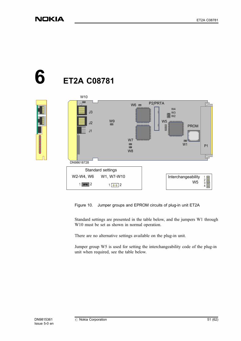
Figure 10. Jumper groups and EPROM circuits of plug-in unit ET2A
Standard settings are presented in the table below, and the jumpers W1 throughW10 must be set as shown in normal operation.
There are no alternative settings available on the plug-in unit.
Jumper group W5 is used for setting the interchangeability code of the plug-inunit when required, see the table below.
W6
W7
W8
W5
W4W3W2
W1
P2/PRTA
J3
J2
J1
DN98618728
W9
W10
P1
PROM
Interchangeability 1234
W5
Standard settings
1 2
W2-W4, W6
1 2
W1, W7-W10
DN9815361Issue 5-0 en
# Nokia Corporation 51 (62)
ET2A C08781

Standard settings (W1-W4, W6-W10)
Table 9. Standard settings of ET2A (W1-W4, W6-W10)
Jumper Setting Meaning
W1;1 - 2 OFF Clock oscillator of processor connected (for testing)
W2;1 - 2 ON Jumper readable by program; not in use
W3;1 - 2 ON Clock oscillator for processor connected (for testing)
W4;1 - 2 ON Processor RESET signal connected (for testing)
W6;1 - 2 ON 6.176 MHz signal connected to interface circuit
W7;1 - 2 OFF -5 V (pin 2) and ground (pin 1) for testing
W8;1 - 2 OFF +5 V (pin 1) and ground (pin 2) for testing
W9;1 - 2 OFF Ground potential for testing
W10;1 - 2 OFF Overvoltage ground of T1 interface separated from digitalground
Interchangeability code settings (W5)
The currently valid interchangeability code is set at the factory.
Table 10. Interchangeability code settings of ET2A (W5)
ICC code W5 setting
1 - 2 3 - 4
A, E, J or N ON ON
B, F, K or P OFF ON
C, G, L or R ON OFF
D, H, M or S OFF OFF
52 (62) # Nokia Corporation DN9815361Issue 5-0 en
ET2A
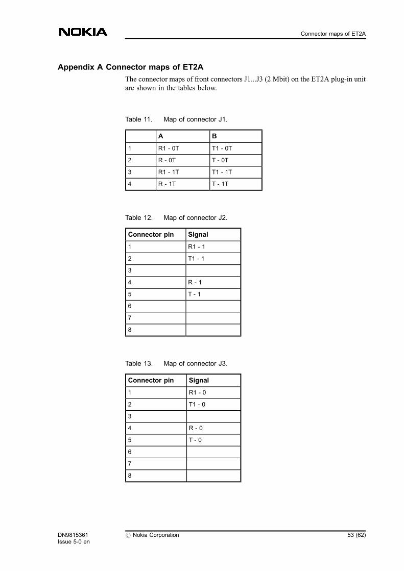
Appendix A Connector maps of ET2A
The connector maps of front connectors J1...J3 (2 Mbit) on the ET2A plug-in unitare shown in the tables below.
Table 11. Map of connector J1.
A B
1 R1 - 0T T1 - 0T
2 R - 0T T - 0T
3 R1 - 1T T1 - 1T
4 R - 1T T - 1T
Table 12. Map of connector J2.
Connector pin Signal
1 R1 - 1
2 T1 - 1
3
4 R - 1
5 T - 1
6
7
8
Table 13. Map of connector J3.
Connector pin Signal
1 R1 - 0
2 T1 - 0
3
4 R - 0
5 T - 0
6
7
8
DN9815361Issue 5-0 en
# Nokia Corporation 53 (62)
Connector maps of ET2A
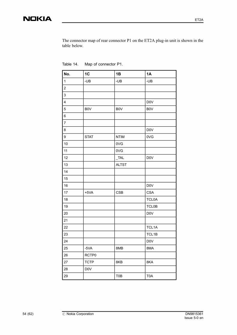
The connector map of rear connector P1 on the ET2A plug-in unit is shown in thetable below.
Table 14. Map of connector P1.
No. 1C 1B 1A
1 -UB -UB -UB
2
3
4 D0V
5 B0V B0V B0V
6
7
8 D0V
9 STAT NTIM 0VG
10 0VG
11 0VG
12 _TAL D0V
13 ALTST
14
15
16 D0V
17 +5VA CSB CSA
18 TCL0A
19 TCL0B
20 D0V
21
22 TCL1A
23 TCL1B
24 D0V
25 -5VA 8MB 8MA
26 RCTP0
27 TCTP 8KB 8KA
28 D0V
29 T0B T0A
54 (62) # Nokia Corporation DN9815361Issue 5-0 en
ET2A
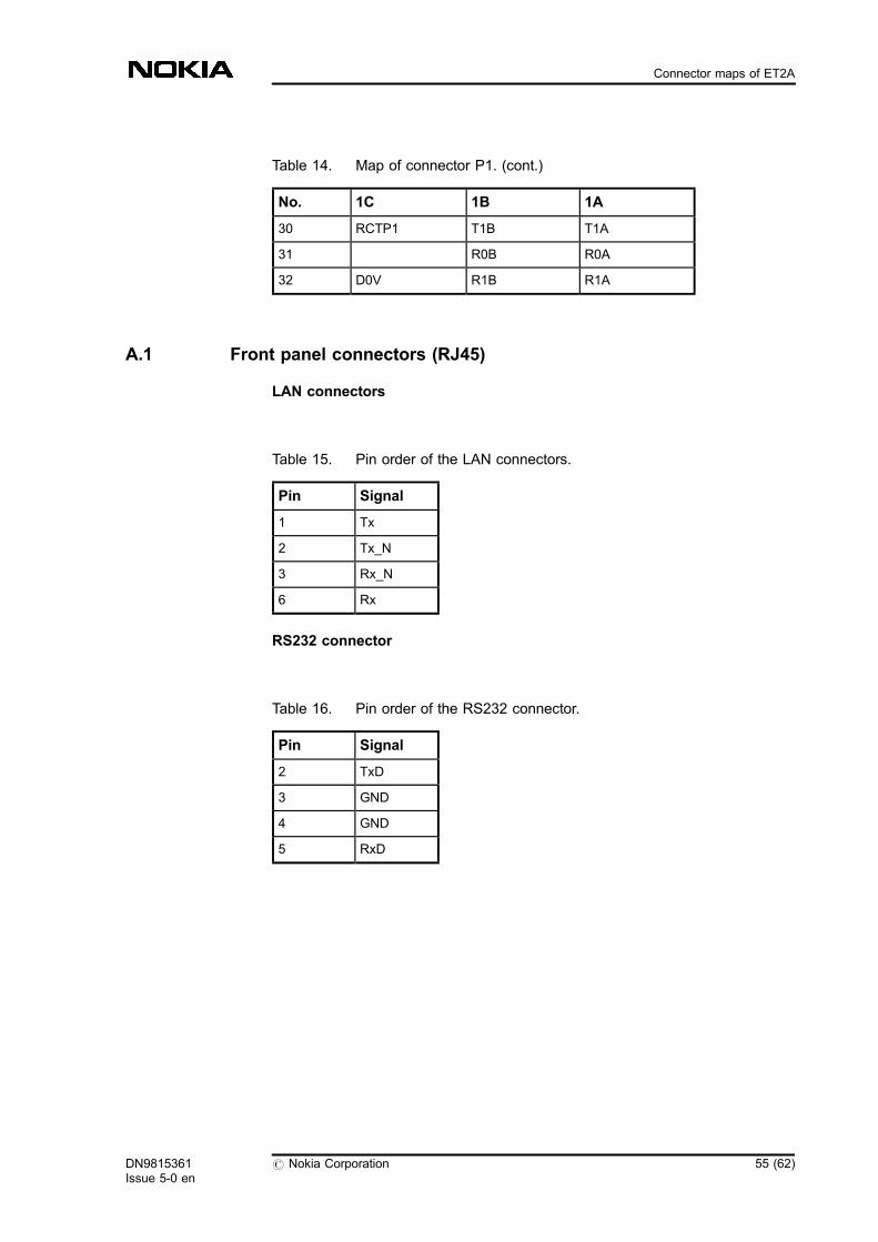
Table 14. Map of connector P1. (cont.)
No. 1C 1B 1A
30 RCTP1 T1B T1A
31 R0B R0A
32 D0V R1B R1A
A.1 Front panel connectors (RJ45)
LAN connectors
Table 15. Pin order of the LAN connectors.
Pin Signal
1 Tx
2 Tx_N
3 Rx_N
6 Rx
RS232 connector
Table 16. Pin order of the RS232 connector.
Pin Signal
2 TxD
3 GND
4 GND
5 RxD
DN9815361Issue 5-0 en
# Nokia Corporation 55 (62)
Connector maps of ET2A

A.2 Backplane connectors
Table 17. Module 1 Backplane Connector
A B C D E
1 UB1 UB1 UB1 UB1 UB1
2
3 BOV1 BOV1 BOV1 BOV1 BOV1
4
5 UB2 UB2 UB2 UB2 UB2
6
7 BOV2 BOV2 BOV2 BOV2 BOV2
8
9 SLOT(0) SLOT(1) SLOT(2) SLOT(3) SLOT(4)
10 HMS_+5V HMS0_+5V SLOT(5) HMS1_+5V GND
11 HMSS_CAN0H HMSS_CAN0L GND HMSS_CAN1H HMSS_CAN1L
12 --- --- --- --- ---
13 --- --- --- --- ---
14 --- --- --- --- ---
15 GND GND GND GND GND
16 SYS_CLK_A+ SYS_CLK_A- GND SYS_CLK_B+ SYS_CLK_B-
17 GND GND GND GND GND
18 JTAG_CLK JTAG_TMS JTAG_RESET JTAG_TDI 1) JTAG_TDO 1)
19 GND
20 GND
21 HMN_VCC SDO1) GND SDI1) ISPEN
22 _HMNISP_EN MODE GND CLK _PWRCTRL
23
24
25
1) SDI and JTAG_TDI inputs are inputs to PIU and SDO and JTAG_TDO outputsare outputs of PIU.
56 (62) # Nokia Corporation DN9815361Issue 5-0 en
ET2A

Table 18. Module 4 Backplane Connector
Z A B C D E F
76 GND RX0_LVDSP RX0_LVDSN GND TX0_LVDSP TX0_LVDSN GND
77 GND GND GND GND GND GND GND
78 GND RX1_LVDSP RX1_LVDSN GND TX1_LVDSP TX1_LVDSN GND
79 GND GND GND GND GND GND GND
80 GND RX2_LVDSP RX2_LVDSN GND TX2_LVDSP TX2_LVDSN GND
81 GND GND GND GND GND GND GND
82 GND RX3_LVDSP RX3_LVDSN GND TX3_LVDSP TX3_LVDSN GND
83 GND GND GND GND GND GND GND
84 GND RX4_LVDSP RX4_LVDSN GND TX4_LVDSP TX4_LVDSN GND
85 GND GND GND GND GND GND GND
86 GND GND GND
87 --- --- --- --- ---
88 --- --- --- --- ---
89 --- --- --- --- ---
90 GND GND GND
91 GND GND GND
92 GND GND GND
93 GND RSVD GND
94 GND RSVD GND
95 GND HMSM_CAN0H HMSM_CAN0L GND GND GND GND
96 GND HMSM_CAN1H HMSM_CAN1L GND GND GND GND
97 GND HMSM_RESET HMSM_TXD GND HMSM_RXD HMSM_BS GND
98 GND + DB(12) + DB(13) GND + DB(14) EN + DB(15) GND
99 GND _DB(12) _DB(13) GND _DB(14) _DB(15) GND
100 GND + DB(0) + DB(1) + DB(2)
+ DB(3) + DB(4) GND
DN9815361Issue 5-0 en
# Nokia Corporation 57 (62)
Connector maps of ET2A
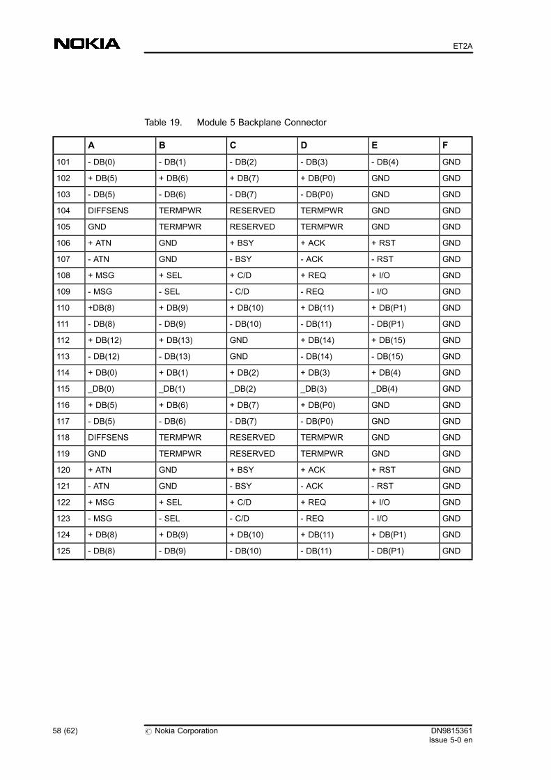
Table 19. Module 5 Backplane Connector
A B C D E F
101 - DB(0) - DB(1) - DB(2) - DB(3) - DB(4) GND
102 + DB(5) + DB(6) + DB(7) + DB(P0) GND GND
103 - DB(5) - DB(6) - DB(7) - DB(P0) GND GND
104 DIFFSENS TERMPWR RESERVED TERMPWR GND GND
105 GND TERMPWR RESERVED TERMPWR GND GND
106 + ATN GND + BSY + ACK + RST GND
107 - ATN GND - BSY - ACK - RST GND
108 + MSG + SEL + C/D + REQ + I/O GND
109 - MSG - SEL - C/D - REQ - I/O GND
110 +DB(8) + DB(9) + DB(10) + DB(11) + DB(P1) GND
111 - DB(8) - DB(9) - DB(10) - DB(11) - DB(P1) GND
112 + DB(12) + DB(13) GND + DB(14) + DB(15) GND
113 - DB(12) - DB(13) GND - DB(14) - DB(15) GND
114 + DB(0) + DB(1) + DB(2) + DB(3) + DB(4) GND
115 _DB(0) _DB(1) _DB(2) _DB(3) _DB(4) GND
116 + DB(5) + DB(6) + DB(7) + DB(P0) GND GND
117 - DB(5) - DB(6) - DB(7) - DB(P0) GND GND
118 DIFFSENS TERMPWR RESERVED TERMPWR GND GND
119 GND TERMPWR RESERVED TERMPWR GND GND
120 + ATN GND + BSY + ACK + RST GND
121 - ATN GND - BSY - ACK - RST GND
122 + MSG + SEL + C/D + REQ + I/O GND
123 - MSG - SEL - C/D - REQ - I/O GND
124 + DB(8) + DB(9) + DB(10) + DB(11) + DB(P1) GND
125 - DB(8) - DB(9) - DB(10) - DB(11) - DB(P1) GND
58 (62) # Nokia Corporation DN9815361Issue 5-0 en
ET2A
A.3 Debug port connector
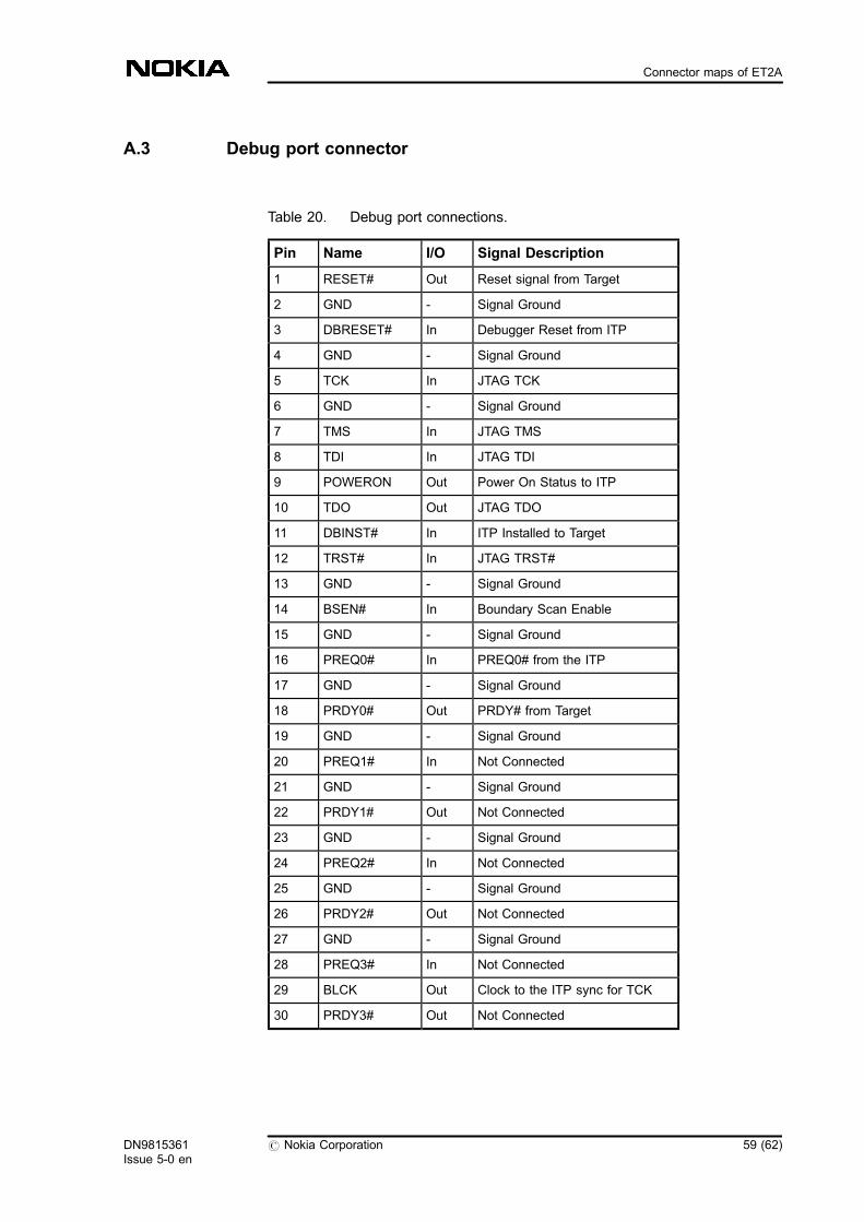
Table 20. Debug port connections.
Pin Name I/O Signal Description
1 RESET# Out Reset signal from Target
2 GND - Signal Ground
3 DBRESET# In Debugger Reset from ITP
4 GND - Signal Ground
5 TCK In JTAG TCK
6 GND - Signal Ground
7 TMS In JTAG TMS
8 TDI In JTAG TDI
9 POWERON Out Power On Status to ITP
10 TDO Out JTAG TDO
11 DBINST# In ITP Installed to Target
12 TRST# In JTAG TRST#
13 GND - Signal Ground
14 BSEN# In Boundary Scan Enable
15 GND - Signal Ground
16 PREQ0# In PREQ0# from the ITP
17 GND - Signal Ground
18 PRDY0# Out PRDY# from Target
19 GND - Signal Ground
20 PREQ1# In Not Connected
21 GND - Signal Ground
22 PRDY1# Out Not Connected
23 GND - Signal Ground
24 PREQ2# In Not Connected
25 GND - Signal Ground
26 PRDY2# Out Not Connected
27 GND - Signal Ground
28 PREQ3# In Not Connected
29 BLCK Out Clock to the ITP sync for TCK
30 PRDY3# Out Not Connected
DN9815361Issue 5-0 en
# Nokia Corporation 59 (62)
Connector maps of ET2A

A.4 PCM connector pin-out
Table 21. PMC Debug Connector, Pn1
Pin Signal Pin Signal
1 ( N.C.) 2 -12VDC
3 GND 4 PCI.~INTA
5 PCI.~INTB 6 PCI.~INTC
7 ( N.C.) 8 +5VDC
9 PCI.~INTD 10 (N.C.)
11 GND 12 (N.C.)
13 @PCI.TSTCLK 14 GND
15 GND 16 PCI.~GNT0
17 PCI.~REQ0 18 +5VDC
19 +5VDC 20 PCI.AD31
21 PCI.AD28 22 PCI.AD27
23 PCI.AD25 24 GND
25 GND 26 PCI.C/~BE3
27 PCI.AD22 28 PCI.AD21
29 PCI.AD19 30 +5VDC
31 +5VDC 32 PCI.AD17
33 PCI.~FRAME 34 GND
35 GND 36 PCI.~IRDY
37 PCI.~DEVSEL 38 +5VDC
39 GND 40 PCI.~LOCK
41 +5VDC 42 (N.C.)
43 PCI.PAR 44 GND
45 (N.C.) 46 PCI.AD15
47 PCI.AD12 48 PCI.AD11
49 PCI.AD9 50 +5VDC
51 GND 52 PCI.C/~BE0
53 PCI.AD6 54 PCI.AD5
55 PCI.AD4 56 GND
57 +5VDC 58 PCI.AD3
59 PCI.AD2 60 PCI.AD1
60 (62) # Nokia Corporation DN9815361Issue 5-0 en
ET2A

Table 21. PMC Debug Connector, Pn1 (cont.)
Pin Signal Pin Signal
61 PCI.AD0 62 +5VDC
63 GND 64 (N.C.)
Table 22. PMC Debug Connector, Pn2
Pin Signal Pin Signal
1 +12VDC 2 (N.C.)
3 (N.C.) 4 (N.C.)
5 (N.C.) 6 GND
7 GND 8 (N.C.)
9 (N.C.) 10 (N.C.)
11 +3.3VDC 12 +3.3VDC
13 PCI.~RST 14 GND
15 +3.3VDC 16 GND
17 (N.C.) 18 GND
19 PCI.AD30 20 PCI.AD29
21 GND 22 PCI.AD26
23 PCI.AD24 24 +3.3VDC
25 IDSEL(PCI.AD16) 26 PCI.AD23
27 +3.3VDC 28 PCI.AD20
29 PCI.AD18 30 GND
31 PCI.AD16 32 PCI.C/~BE2
33 GND 34 (N.C.)
35 PCI.~TRDY 36 +3.3VDC
37 GND 38 PCI.~STOP
39 PCI.~PERR 40 GND
41 +3.3VDC 42 PCI.~SERR
43 PCI.C/~BE1 44 GND
45 PCI.AD14 46 PCI.AD13
47 GND 48 PCI.AD10
49 PCI.AD8 50 +3.3VDC
51 PCI.AD7 52 (N.C.)
DN9815361Issue 5-0 en
# Nokia Corporation 61 (62)
Connector maps of ET2A
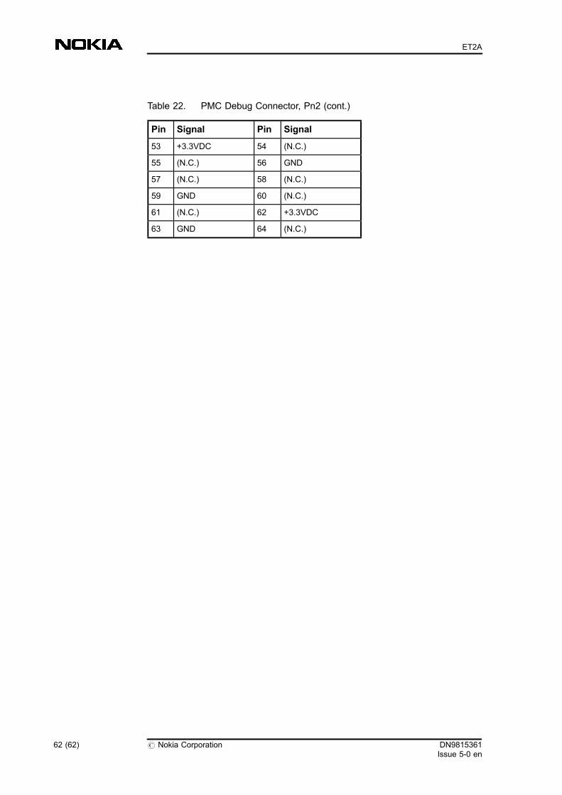
Table 22. PMC Debug Connector, Pn2 (cont.)
Pin Signal Pin Signal
53 +3.3VDC 54 (N.C.)
55 (N.C.) 56 GND
57 (N.C.) 58 (N.C.)
59 GND 60 (N.C.)
61 (N.C.) 62 +3.3VDC
63 GND 64 (N.C.)
62 (62) # Nokia Corporation DN9815361Issue 5-0 en
ET2A