Embed Size (px)
Citation preview

Plasma Chemistry and Plasma Processing, Vol. 19, No. 4, 1999
Etching of Silicon Nitride in CCl2F2, CHF3, SiF4, andSF6 Reactive Plasma: A Comparative Study
B. D. Pant1 and U. S. Tandon1
Received January 22, 1997; revised February 3, 1999
Silicon nitride is an important material layer in various types of microelectronicdevices. Because of continuous integration of devices, patterning of this layerrequires a highly selective and anisotropic etching process. Reactive ion etching isone of the most simple and popular plasma processes. The present work is an exper-imental analysis of primary etch characteristics in reactive ion etching of siliconnitride using chlorine- and/or fluorine-based organic and inorganic chemistries(CCl2F2+O2, CHF3+O2, SiF4+O2, SF6+O2, and SF6+He) in order to obtaina simultaneous etch selectivity against polysilicon and silicon dioxide. A recipe, inCCl2F2/O2 plasma chemistry, which provides acceptable etch characteristics, alongwith a reasonable simultaneous selectivity against polysilicon and silicon dioxide,has been formulated.
KEY WORDS: Anisotropy; etch characteristics; isolation; selectivity; trench.
1. INTRODUCTION
Silicon nitride (Si3N4) has a wide variety of applications in the fabri-cation of silicon semiconductor devices, such as memory,(1) electro-opticaland CMOS devices.2,3 One of the significant applications of silicon nitrideis in masks for X-ray lithography.(4) With the downward scaling of mono-lithic ICs, the role of silicon nitride is continuously increasing, especially inisolation techniques such as LOCOS, SWAMI, TRENCH, OSELO, andSILO.(5-10) Therefore, the etching of Si3N4 needs critical control over theetch rate, selectivity(11) (against the masking and underlayers, especially thinSiO2), and etch profile.(12) Various research workers, in order to achievethe desired characteristics, have extensively studied plasma etching of thismaterial layer. Different reactive gases investigated for this purpose includehalocarbons, such as CF4, CHF3, etc, and inorganic reactive gases, NF3
and SiF4, etc. Selectivity with respect to silicon dioxide in halocarbon
1Microelectronics Technology Group, Solid State Devices Area, Central Electronics Engineer-ing Research Institute, Pilani 333031, India.
5450272-4324/99/1200-0545$16.00/0 © 1999 Plenum Publishing Corporation

plasmas had been a severe problem. A lot of effort was put in to achievethis important characteristic either through process design or reactor design,or a combination of both approaches. Freon-14 (CF4) was found to be mosteconomic and popular reactive gas for the plasma etching of dielectrics,including silicon nitride. In the early 1970s, Adir Jacob,(13) pioneered theplasma etching of silicon nitride in CF4-based plasmas using a barrel reac-tor. Since then, much work in CF4-based plasma processes has beenreported(14-20) using different kinds of plasma sources (low- and high-pressure RF, ECR, TCP, HCP, ICP, etc.) and reactor configurations (hex-ode, barrel, tunnel, parallel plate, downstream, etc.) for the etching of siliconnitride. It has been established that a high selectivity against silicon dioxide,particularly in halocarbon plasma, is very difficult to achieve. However, ithas been achieved in microwave plasma processes. Recently, Kastenmeiret al.(19) have reported a chemical dry etching process for Si3N4/SiO2 in adownstream microwave (GHz) plasma reactor using CF4 as a reactive gas.They have achieved very good selectivity through the incorporation of O2
and N2 in a downstream microwave plasma process. Nitrogen plays asignificant role in the increased etch rates of nitride and selectivity againstsilicon dioxide. They have suggested an etching mechanism to explain thisphenomenon. In another work, Grykewich et al.(20) have reported a mask-dependent selectivity against silicon dioxide in CF4/O2. A number of otherhalocarbons(21-24) have also been investigated for the etching of Si3N4/SiO2.Ying Zhang et al.(24) showed that the hydrogen-rich fluorocarbon gases ortheir mixtures, which contain less carbon e.g., CHF3/H2 are useful for selec-tive etching of Si3N4 over SiO2.
(25-30) However, the selectivity against SiO2
has been achieved through the addition Of O2,17,19,20,23,27,30,31) N2,
(19) NH3,(31)
and Cl2 .(32) Most of these processes, including the microwave plasma pro-
cesses, have either the disadvantage of high ratio of O2 in the mixture, whichleads to the loss of lateral dimensions of the etched patterns, or corrosionproblems (for the processes with chlorine additives). Another reactive gasNF3
(33) has been reported to provide moderate selectivity for silicon nitrideagainst silicon dioxide in RF plasma. In this process, CCl2F2 has been usedas an additive to improve the selectivity against silicon dioxide, but theselectivity against polysilicon is doubtful. Reactive gas SiF4 has also beenreported(34,35) to provide selectivity against silicon dioxide. However, it isnot free from depositions. On the other hand, SF6-based plasma processeshave provided a very high selectivity against silicon dioxide, but, again, theselectivity with respect to polysilicon would be a problem. Therefore, theexisting RF reactive plasma processes for the etching of silicon nitride areeither selective to polysilicon or to silicon dioxide. Thus, simultaneous selec-tivity is a problem. The present work aims at the development of a process,which provides a simultaneous selectivity against silicon dioxide and
546 Pant and Tandon
polysilicon. We have investigated a number of chlorine- and/or fluorine-containing organic and inorganic chemistries based on four reactive gases,CCl2F2, CHF3, SiF4, and SF6 to obtain a reasonable etch selectivity againstsilicon dioxide as well as polysilicon, in the reactive ion etching (RIE) ofSi3N4. In particular, Freon-12 (CCl2F2), which has not, thus far, been inves-tigated as a main reactive gas, was explored in detail in the present workfor the RIE of silicon nitride. An analytical comparison of important etchcharacteristics have been made using five plasma chemistries and the mostuseful formulation has been suggested.
The characteristics of a dry etching process are numerous(36) the mostimportant of which are the etch rate, selectivity, and anisotropy. We wouldcall these three parameters the primary etch characteristics. The first onegoverns the speed of the process and is useful in controling throughput—a high etch rate is desirable for high throughputs. The second importantcharacteristic is the selectivity against masking and underlayers. Withoutproper selectivity, correct transfer of a desired pattern onto the layer ofinterest cannot be achieved. The third one is the control over the etch pro-file. It has its implication over the feature integrity. The other etch charac-teristics are uniformity, reproducibility, residue or deposition-free etch, andfreedom from physical and radiation damages, which can be taken care ofin different ways.(37)
The etch characteristics discussed above are the composite functions ofa score of interdependent process parameters.(38) However, the etch chemis-try is the single largest variant having the most influence compared to allother process parameters on the primary etch characteristics(39) Therefore,the chemical composition of etch gas can be varied to obtain the best selec-tivity in a specific set of process parameters. In the present work, we estab-lish that the reactive gases, viz., CCl2F2, CHF3, SiF4, and SF6, withoxidizing and/or neutral additives, could be used to achieve a reasonablygood selectivity against both SiO2 and polysilicon in the RIE of siliconnitride.
2. EXPERIMENTAL
Samples used for this work consist of both patterned and unpatternedLPCVD silicon nitride, thermally grown silicon dioxide and LPCVD poly-silicon on p-type (100) silicon wafers of 50-mm diameter. The nitridesamples had an initial nitride thickness of 1500° A with an underlying silicondioxide of 1000 thickness. The vertical etch rates were determined by pre-and postetch thickness of three layers on independent wafers using theNanospec thickness measurement system. The lateral etch rates were
Etching of Silicon Nitride 547
deduced from the pre- and postetch linewidths of a group of lines. A high-resolution photoresist HPR 204 from Hunt Chemicals (USA) was used forpatterning the samples.
The etching experiments were conducted in Anelva DEA 506M parallelplate batch reactor. The reactor chamber is composed of 316 stainless steel.It consists of a rotating (5 RPM) water-cooled cathode and a perforatedanode. The interelectrode spacing can be varied from 10 to 110mm usingspacers. Samples were placed horizontally over the cathode of a diameterof 50cm. A Teflon cover on the cathode was used for all Freon-basedplasmas whereas a quartz cover replaced it for chlorine-based plasma(CCl2F2) processes. All the process parameters, except the substratetemperature and the DC bias, were monitored directly. The cathode tem-perature was, however, maintained between 55 and 60°C in all experimentsindirectly through interative control of the temperature of the cooling watercirculated through the cathode. The DC bias, in fact, has a complex depen-dence on all other process parameters.
3. RESULTS AND DISCUSSIONS
The primary etch characteristics, viz., etch rate, selectivity against themasking and underlayer, and anisotropy in the RIE of silicon nitride are acomplex function of a number of process parameters, etch chemistry beingthe most important among them. As already stated, five etch chemistrieswere chosen for an analysis of the primary etch characteristics. Throughinitial gauging experiments the etch pressure and interelectrode distancewere optimized at 10 Pa and 70mm, respectively. The ratio (vol.%) of theoxygen/nitrogen or helium in the reactive gas mixture was investigated (bycontinuously increasing its ratio in the mixture) for the optimum values ofthe primary etch characteristics. The gases used for CCl2F2, SiF4, CHF3,and SF6, are either fluorine and/or chlorine based and provide F, Cl, CFX,and CCly-type fragments and ions, which react with Si in Si3N4 to convertit to volatile products(40) The possible empirical reactions are:
With polysilicon and SiO2, the following reactions dominate:(41,42)
548 Pant and Tandon

Etching of Silicon Nitride 549
Fig. 1. Variation in the etch rates of silicon nitride, silicon dioxide, and polysilicon with thevol.% of oxygen in (CCl2F2 + O2) reactive plasma at a total flow rate of 50 SCCM, 600 W RFpower (13.56 MHz), and 10 Pa etch pressure.
There are at least five sequential primary steps in a typical RIEprocess(43) The generation of reactive species essential for the etching ofsilicon nitride in a reactive plasma is dependent upon the RF power, flowrate, and etch pressure for a given reactor configuration. These processparameters have been fixed at certain values for all the etching recipes ana-lyzed in order to compare the etch characteristics. Hence, the residence timefor reactive species in all plasma chemistries except one (CHF3 + O2 chemis-try) was fixed at 5.68m/s. In CHF3 + O2 plasma, it was not possible toobtain a desired selectivity against silicon dioxide at the etch pressure of10 Pa (set for all the processes). We have observed that a considerable selec-tivity against SiO2 can be achieved at an etch pressure of 15 Pa and, hence,the residence time comes out to be 8.52 m/s.
One of the biggest problems with the RIE of silicon nitride is that thespecies reactive to silicon nitride are almost equally reactive to silicon diox-ide and also, to a great extent, to polysilicon.(38,44) Therefore, it is very diffi-cult to devise a recipe, that provides acceptable selectivity in the reactive

plasma etching of silicon nitride against silicon dioxide and polysilicon sim-ultaneously. Nevertheless, the present study reveals that the importantplasma etch characteristics can be tailored through the judicious selectionof etch chemistry and optimization of the process parameters. We will nowdiscuss the results obtained with different plasma chemistries.
Freon-12 (CCl2F2) is a gas which provides both Cl and F species in itsplasma and, hence, can be used for the reactive plasma etching of siliconnitride. Thus far, there is hardly any work reported using Freon-12 as amain etching gas for the etching of silicon nitride. The addition of a smallpercentage of gas in plasma has been reported(33) to enhance the selectivityof silcon nitride against silicon dioxide. A very high selectivity against sili-con dioxide has been recently reported(31,45,46) using NF3 with O2/NH3/N2
in microwave plasma processes. However, selectivity against polysilicon inNF3-based plasma is again a problem. In the present work we have devised arecipe, based in Freon-12, which is able to provide a simultaneous selectivityagainst both the SiO2 and polysilicon layers. We have observed that the etchrates of silicon nitride and selectivity against SiO2 and polysilicon are ratherlow in CCl2F2 RIE without any additive. The addition of inert additives(He, Ar) enhances etch rates but not selectivity. On the contrary, an oxidiz-ing additive, e.g., O2, enhances etch rate and selectivity against SiO2 andpolysilicon. Figure 1 shows the variation in etch rates of the three materiallayers: Si3N4, SiO2, and polysilicon with the variation of vol.% of O2 in themixture. We observe that the etch rates are lower for both silicon nitrideand silicon dioxide, with the lower ratios of oxygen in the mixture. Withthe increase of O2, a rise in etch rates is observed. Empirically, CCl2F2
breaks into a number of fragments in plasma:
550 Pant and Tandon
The initial low etch rates at lower ratios of oxygen in the mixture canbe attributed to the lower steady state concentrations of F and Cl speciesbecause of their recombination with the carbon atoms and unsaturated spec-ies, as is clear from Eq. (8). With an increase of oxygen in the mixture, thecarbon atoms are converted to CO or CO2, as shown in Eq. (9). As anoutcome, the recombination of F and Cl species with carbon decreases lead-ing to an increase in the number of etch species. This results in an increasein etch rates. This increase in etch rates of Si3N4, however, stops at 35-vol.% of O2 in the mixture. We reach a maximum etch rate of 378 A/min.Obviously, the further generation of reactive species is replaced by oxygenatoms of the feed gas. If we further increase the ratio of O2 in the mixture,it keeps reducing F and Cl concentrations and, thereby, a reduction in etch

Etching of Silicon Nitride
Fig. 2. SEM micrograph of a group of equidistant lines etched in 40 SCCM CCl2F2 + 10 SCCMO2 at 10 Pa etch pressure and 600 W RF power.
rate is observed. The etch rate of polysilicon also shows a similar behavior,although the rate of increase is rather low; it attains a maximum value of192.5A/min at 43% of O2. With this behavior, the selectivity of Si3N4
against polysilicon increases with the addition of O2 up to 35% in the mix-ture. The SiO2 etch rates in this chemistry are rather low and continuouslydecrease with increase in the ratio of O2. Therefore, as O2 is added, theselectivity against SiO2 increases at a faster rate in comparison to theincrease in selectivity against polysilicon.
We observe that the peaks of etch rates in this chemistry for Si3N4 andfor polysilicon do not coincide. These observations can be explained byconsidering the plasma and the surface chemistry involved. Oxygen plays asignificant role. Initially, for the lower ratios of O2 in the mixture, it is notavailable for physi- and/or chemisorption on etch surface. It is more or lessconsumed completely by the C atoms present in the plasma, resulting involatile products CO and CO2. As already stated, we observe a continuousincrease in etch rates with the increase of O2. If O2 is increased beyond its
551

consumption by C atoms, it becomes available for absorption on the differ-ent surfaces present, the etch surface being one of them. Because of thisbehavior, the maximum etch rate for Si3N4 occurs at 35% of O2 in themixture. In the case of polysilicon, though, it has a larger affinity with O2
in comparison to that of Si3N4, yet the absorbed O2 moves down to theintergrain regions, leaving a very thin layer of O2 on the top. This thin layeris vulnerable to ion bombardments, maintaining access of etch species tothe bulk. A greater amount of O2 is, therefore, required to retard the flowof etch species to the bulk. Hence, the peak in etch rate appears at a higherratio i.e., 43% of O2 in the mixture. In the case of SiO2, a slow decrease inetch rates with increase in O2 in the mixture may be attributed to thedilution of etch species.
The etch uniformity in this chemistry was found to be very good (betterthan 97% over a wafer of 50-mm diameter) at a ratio of 25 to 33% of oxygenin the mixture. It decreases very sharply with the increase in oxygen beyond33 vol.% in the mixture. At 50 vol.% of O2, the selectivity decreases to 78%.The percentage loss of linewidth for 1500 A thick silicon nitride is 6%;hence, the lateral loss of the etched patterns is quite low. Figure 2 is a SEMmicrograph of a group of lines etched in 40 SCCM CCl2F2, 10 SCCM O2 at10 Pa etch pressure and 600 W RF power. We observe that the surface isclean and smooth. There is no visible physical damage to the etched surface.The various process and characterization parameters related to this processare tabulated in Table I.
Freon-23 (CHF3) is a reactive gas widely used for the etching of silicondioxide.25,26 It can also be used for the etching of silicon nitride throughjudicious control of process parameters,(25-30) particularly, the chemistry andetch pressure. We have observed that although it gives a poor selectivityagainst SiO2 in a particular range of the etch pressure (8-12 Pa), a reason-able selectivity has been obtained above a certain critical pressure. It sup-ports the findings by Dulak et al.(47) CHF3 + O2 plasma has a behavior quitesimilar to CF4 + O2 plasma in the etching of Si3N4/SiO2. Many of theresearchers have investigated CF4 chemistry in detail in an effort to obtainsuitable primary etch characteristics for these two materials. A high selec-tivity against silicon dioxide in microwave plasma has been reported,(19)
which is rather difficult to obtain in RF plasma. However, the mixture ofhalocarbons with reducing or oxidizing additives has been reported to pro-vide a reasonable selectivity against silicon dioxide. Most of these processeshave a disadvantage of high ratio of O2 in the mixture, which leads to theloss of lateral dimensions of the etched patterns. We have, in the presentwork, chosen CHF3, which can deliver reasonable simultaneous selectivityagainst SiO2 and polysilicon, respectively, along with anisotropy. The,addition of N2, in a subsequent experiment, has shown only a moderate
552 Pant and Tandon

Etching of Silicon Nitride 553

554 Pant and Tandon
Fig. 3. Variation in the etch rates of silicon nitride, silicon dioxide, and polysilicon with thevol.% oxygen in (CHF3 + O2) reactive plasma at a total flow rate of 50 SCCM, 600 W RFpower (13.56 MHz), and 15 Pa etch pressure.
improvement in the selectivity (increases to 3.1) against SiO2 in our process.Figure 3 shows the variation in etch rates of three material layers, viz.,Si3N4, SiO2, and polysilicon with the increase in vol.% of O2 in the mixtureof CHF3 and O2 as reactive gas at an etch pressure of 15 Pa and RF powerof 600 W. It is observed that etch rate and selectivity for the etching of Si3N4
are rather low for very low concentrations of O2 in the mixture, supportingfindings by some of the researchers.(17,19,20,23,27,30) With the increase of oxy-gen, the Si3N4 etch rate initially rises to a maximum of 776 A/min at 40%of O2 in the mixture. The selectivity against polysilicon and SiO2 also attainmaximum values of 11.0 and 1.9, respectively. A further increase in selec-tivity up to 3.1 has been achieved in a subsequent experiment through 12%incorporation of nitrogen while retaining the volume ratio of CHF3 to O2
equal to 4:1.

Etching of Silicon Nitride
Fig. 4. SEM micrograph of 2 x 2 micron contact holes etched in nitride with 40 SCCMCHF3 + 10 SCCM O2 at an etch pressure of 15 Pa and 600 W RF power. The top and bottomsurfaces are virtually free from any type of deposition and physical damage.
The rapid increase in etch rates of Si3N4 can be understood throughthe role of O2 in the mixture. Initially, when there is no oxygen, the recombi-nation of different species and fragments results in lower steady state con-centrations of the etch species, in addition to the formation of thin polymerlayers of unsaturated fluorocarbon fragments on Si3N4, resulting in loweretch rates. As soon as oxygen is introduced, it oxidizes the fluorocarbonfragments, which ultimately results in a considerable increase in etch species.It also forms volatile oxides of nitrogen present in the silicon nitride. Theformation of nitric oxide (NO) in the plasma has direct relation to the Si3N4
etch rate. It has recently been established(19) that NO molecule or metastableNO plays a significant role in the etching of Si3N4 through active surfacereactions. In addition to these, the fluorocarbon polymer film, which isdeposited over Si3N4 during oxygen-deficient plasma, is decomposed quicklyand is evaporated as CO or CO2. The total effect is a rapid increase in theetch rates. The fall in etch rates beyond 40% of O2 in the mixture is basicallybecause of the dilution of the reactive species by oxygen itself. The effect of
555
556 Pant and Tandon
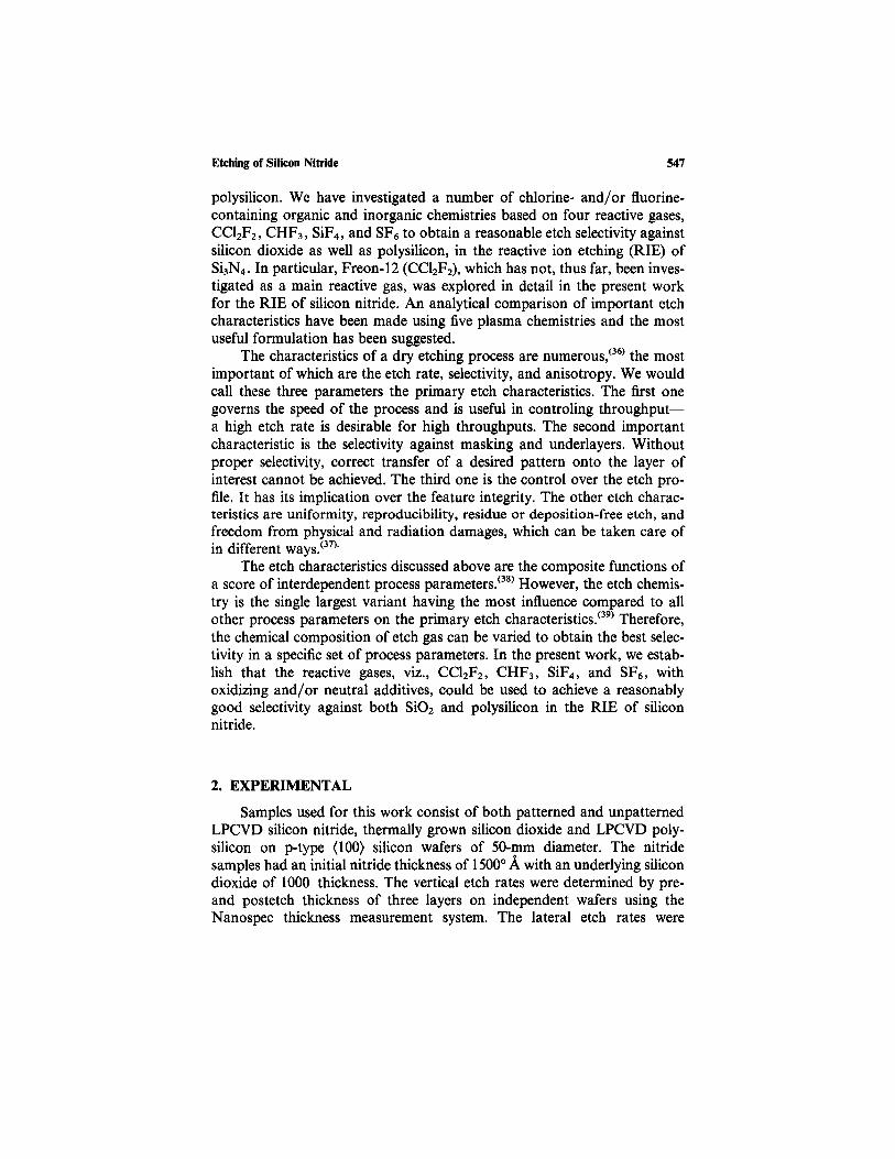
increase of oxygen in the mixture onto the silicon dioxide and polysiliconetch rates is not very significant, both of them demonstrate a slow decrease.Etch uniformity obtained in this recipe is reasonably good (86%). The pro-cess and characterization parameters for a typical process comprised of15 Pa etch pressure, 600 W RF power, and with a total flow of 50 SCCMin CHF3/O2 has been given in Table I. Figure 4 is a SEM micrograph of2 x 2 um contact holes etched in nitride with 40 SCCM CHF3 + 10 SCCM O2
at an etch pressure of 15 Pa and 600 W RF power. The top and bottomsurfaces are virtually free from any kind of deposition and physical damage.
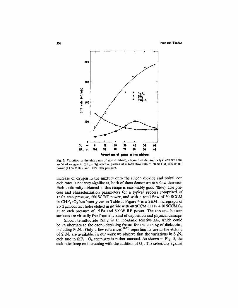
Silicon tetrafluoride (SiF4) is an inorganic reactive gas, which couldbe an alternate to the ozone-depleting freons for the etching of dielectrics,including Si3N4. Only a few references(34,35) reporting its use in the etchingof Si3N4 are available. In our work we observe that the variations in Si3N4
etch rate in SiF4 + O2 chemistry is rather unusual. As shown in Fig. 5, theetch rates keep on increasing with the addition of O2. The selectivity against
Fig. 5. Variation in the etch rates of silicon nitride, silicon dioxide, and polysilicon with thevol.% of oxygen in (SiF4 + O2) reactive plasma at a total flow rate of 50 SCCM, 600 W RFpower (13.56 MHz), and 10 Pa etch pressure.

Etching of Silicon Nitride
Fig. 6. One micron line etched in 40 SCCM SiF4+ 10 SCCM O2 at a total flow rate of 150SCCM, 600 W RF power, and 10 Pa etch pressure A polymer type deposition was observed.
photoresist is 6.4, which is reasonably good. A polymer-type depositionwas observed in this process (Fig. 6). It is because of the deposition of theunsaturated molecules forming a thin film over silicon and silicon nitridesurfaces. Photoresist nibbling, up to some extent, was also observed in theprocess. The etch rates are rather low for lower concentrations of O2 in themixture. However, the etch rates shoot up sharply with the increase of oxy-gen in the mixture. The selectivity against polysilicon also increases as theincrease in the etch rates of polysilicon is much slower compared to that ofsilicon nitride. Selectivity against silicon dioxide increases sharply beyond8% O2 in the mixture. Selectivity against photoresist is also reasonably good(typical value 6.4), but the lateral loss of the etched patterns is higher—16.4% for 1500 A thick nitride.
Sulfur hexafluoride (SF6) has been the conventional reactive gas for theRIE of polysilicon/Si.(48-51) It can, however, be used for the RIE of siliconnitride. Therefore, selectivity for silicon nitride against polysilicon inSF6 + O2 plasma is a problem. We have carried out a detailed investigationof the etch rates and selectivity for the silicon nitride. The selectivity against
557

558 Pant and Tandon
SiO2 is reasonably good in this chemistry, caused by high concentrations ofF atoms in the plasma. For the lower ratios of oxygen, F atom concen-tration is limited by its recombination with S atoms. An increase of O2 inthe mixture removes the S atoms in the form of volatile SO2, increasing theF atom concentration and, in turn, the etch rate of Si3N4. Figure 7 showsthe variation in etch rates of silicon nitride and silicon dioxide with theincrease of oxygen in the mixture. It is observed that the Si3N4 etch ratesincrease very sharply up to 30% O2, and tend to stabilize between 30 to40%. On the contrary, the SiO2 etch rates are more or less constant, a steadyincrease in the etch rates up to 30% of oxygen and then a fall is observed.The selectivity against SiO2 increases slowly with the addition of O2 up to30% O2 in the mixture, whereas between 30 to 40% O2, the increase inselectivity is very fast because of the decrease in SiO2 etch rates beyond 30vol.% of O2 in the mixture. One of the problems in this plasma process is a
Fig. 7. Variation in the etch rates of silicon nitride and silicon dioxide with the vol.% of oxygenin (SF6 + O2) reactive plasma at a total flow rate of 50 SCCM, 600 W RF power (13.56 MHz),and 10 Pa etch pressure.

Etching of Silicon Nitride
lower selectivity against photoresist, the best being 1.9. Obviously, itdecreases with the addition of oxygen in the mixture. SF6/O2 provides avery clean etch, although somewhat nonuniform (81% uniformity). Figure8 shows a few mesa structures of dimensions 6x6 um etched in 40 SCCMSF6 + 10 SCCM O2, RF power of 600 W, and etch pressure 10 Pa. Introduc-tion of an inert gas (helium) in place of oxygen in the reactive gas mixturewas found to predictably contribute to the sputter etch section in the RIE.The initial low etch rates (600 A/min, Fig. 9) at lower ratios of He in the(SF6 + He) mixture are improved to 1000 A/min, because of the sputter etchmechanism of the RIE process. The process provides more anisotropic etch-ing with a likelihood of electrical damage to the underlayer, which could beminimized through the judicious selection of the RF power density. Inanother approach one can choose a two-step plasma process. The first onecomprised of a highly anisotropic step, while the second one highly selectiveto the underlayer. Selectivity against silicon dioxide is 12.3, which is slightlylower than that obtained in SF6/O2 plasma chemistry. In this process, selec-tivity against the photoresist is improved to 2.2 and the loss of lateral dimen-sions is reduced to 9.9% for 1500 A thick nitride patterns. Figure 10 is a
Fig. 8. Mesa structures of dimensions 6 x 6 um etched in a recipe comprised of 40 SCCMSF6+ 10 SSCM O2 at an RF power 600 W and etch pressure 10 Pa.
559

560 Pant and Tandon
micrograph of 2x2 um holes etched in silicon nitride using an SF6/Heplasma with a total flow of 50 SCCM, 600 W RF power, and 10 Pa etchpressure.
4. CONCLUSIONS
A comparison of five RIE processed based on CCl2F2, CHF3, SiF4 andSF6 reactive RF (13.56 MHz) plasma for the etching of silicon nitride hasbeen made. The typical process parameters and the etch characteristics (etchrates, selectivity against the photoresist, silicon dioxide, polysilicon, the per-centage loss of linewidth of the patterns of thickness 1500 A in silicon nitrideand uniformity) obtained for the five recipes are summarized in Table 1.
It has been observed that oxygen addition has a significant effect inthe improvement of primary etch characteristics of silicon nitride. In RF
Fig. 9. Variation in the etch rates of silicon nitride and silicon dioxide with the vol.% of heliumin (SF6 + He) reactive plasma at a total flow rate of 50 SCCM, 600 W RF power (13.56 MHz),and 10 Pa etch pressure.

Etching of Silicon Nitride
(13.56 MHz) plasma processes, we have observed that CCl2F2/O2 andCHF3 /O2 plasma based RIE processes are capable of delivering a reason-able simultaneous selectivity against polysilicon and silicon oxide, yet theearlier one has a clear edge in anisotropy and deposition-free etch surfaces.The later one, i.e., CHF3/O2 could be used effectively in the fabricationprocesses where one can sacrifice a marginal loss of the lateral dimensionof the etched patterns. It provides a relatively higher selectivity against poly-silicon. For a highly anisotropic etching one, can use SF6/O2 selectivelyagainst silicon dioxide. More effectively, one can choose a two-step processbased on two different plasma chemistries, depending upon a particularrequirement.
ACKNOWLEDGMENTS
The continuous support by our Lithography, Scanning ElectronMicroscopy, Oxidation, Chemistry, and Materials Growth facility teams isthankfully acknowledged.
Fig. 10. Micrograph of 2x2 um holes etched in silicon nitride using an SF6/He plasma witha total flow of 50 SCCM, 600 W RF power, and 10 Pa etch pressure.
561

REFERENCES
1. M. K. Mazumder, K. Kobayashi, Tamotsu Ogata, J. Mitsuhashi, Y. Mashiko, andH. Koyatna, J. Electrochem. Soc. 143, 368 (1996).
2. R. A. Colclaser, Microelectronic Processing and Device Design (Academic Press, NY, 1980),p. 47.
3. Yue Kuo, J. Electrochem. Soc. 142, 186 (1995).4. U. S. Tandon, B. D. Pant, and Ashok Kumar, Vacuum 42, 1219 (1991).5. K. Nojiri, K. Tsunokuni, K. Horibe, K. Ito, and S. Kishino, Extended Abstr. 17th Conf.
Solid State Devices Mater, p. 337 (1985).6. K. Shiozawa, T. Oishi, H. Maeda, T. Murakami, K. Yasumura, Y. Abe, and Y. Tokuda,
J. Electrochem Soc. 145, 1684 (1998).7. V. K. Dwivedi, J. Electrochem Soc. 137, 2586 (1990).8. S. Deleonibus, P. Molle, L. Tosti, and M. C. Taccusel, J. Electrochem. Soc. 138, 3739
(1991).9. D. C. Gray, J. W. Butterbaugh, C. F. Hiatt, A. S. Lawing, and H. H. Sawin, J. Electro-
chem. Soc. 142, 3919 (1995).10. S. S. Cooperman, A. I. Nasi, and G. J. Grula, J. Electrochem. Soc. 142, 3180 (1995).11. W. Grynkewich, T. H. Fednyshyn, and R. H. Dumas, J. Vac. Sci. Technol. B 8, 5 (1990).12. Haselden, P. Peavy, B. Eliscon, and T. Ahmed, Proc. SPIE-Intern. Soc. Opt. Eng. 115,
1185(1990).13. A. Jacob, U. S. Patent 3,795,557 (1974).14. H. M. Sanders, J. Dieleman, H. J. B. Peters, and J. A. M. Sanders, J, Electrochem. Soc.
129, 2559 (1983).15. Field, D. F. Klenperer, and I. T. Wade, J. Vac. Sci. Technol. B 6, 551 (1988).16. C. J. Mogab, A. C. Adams, and D. L. Flamm, J. Appl. Phys. Lett. 49, 3796 (1978).17. G. Smolinsky and D. L. Flamm, J. Appl. Phys. 50, 982 (1979).18. Y. Zhang, G. S. Oehrlein, G. M. W. Kroesen, M. Mittmer, and Stein, J. Electrochem.
Soc. 140, 1439 (1993).19. B. E. E. Kastenmeir, P. J. Matsuo, and G. S. Oehrlein, J. Vac. Sci. Technol. A 14, 2802
(1996).20. G. W. Grykewich, T. H. Fedynyshyn, and R. H. Dumas, J. Vac. Sci. Technol. B 8, 5
(1990).21. L. M. Ephrath, J. Electrochem. Soc. 126, 1419 (1979).22. Ho-Jun Lee, Joong Kyun Kim, Jung Hun Kim, and Ki-Woong Whang Jeong Jeong Ho
Kim, and Jung Hoon Joo, J. Vac. Sci. Technol. B 16, 500 (1998).23. Histaka Hayashi, Kazuaki Kurihara, and Makoto Sekine, Jpn. J. Appl. Phys. 35, 2488
(1996).24. Ying Zhang, G. S. Oehrlein, and F. H. Bell, J. Vac. Sci. Technol. A 14, 2127 (1996).25. H. Toyoda, M. Tobinaga, and H. Komiya, Jpn. J Appl Phys. 20, 681 (1981).26. D. H. G. Choe, C. Knapp, and A. Jacob, Solid State Technol. 27, 177 (1984).27. T. K. S. Wong and S. G. Ingram, J. Vac. Sci. Technol. B 10, 2393 (1992).28. A. M. Barklund and H. O. Blom, J. Vac. Sci. Technol. A 11, 1226 (1993).29. Y. X. Li, M. Laros, P. M. Sarro, P. J. French, and R. F. Wolffenbuttel, Microelectr. Eng.
20, 321 (1993).30. P. E. Riley, B. N. Defonseka, J. C. Sum, and D. Figueredo, IEEE Trans. Semicond. Manuf.
6, 290 (1993).31. Ying Wang and L. Luo, J. Vac. Sci. Technol. A. 16, 1582 (1998).32. D. E. Ibbotson, J. A. Mucha, D. L. Flamm, and J. M. Cook, Appl. Phys. Lett 46, 794
(1985).
562 Pant and Tandon

33. Barkanic, D. M. Reynolds, R. J. Jaccodine, H. G. Stenger, J. Parks, and M. Vedage,Solid State Technol. 32, 109 (1989).
34. H. Boyd and M. S. Tang, Solid State Technol. 22, 133 (1979).35. E. P. G. T. van de Yen and P. A. Zijlstra, Proc. Electrochem. Soc. 81, 112 (1981).36. J. W. Couburn, J. Plasma Chem. Plasma Process. 2, I (1982).37. B. Gorowitz and R. J. Saia, VLSI Electronics, Vol 8, Series Editor G. Norman, ed. (Aca-
demic Press, Orlando, Florida, 1984), p. 298.38. P. E. Riley and D. A. Hanson, J. Vac. Sci. Technol. B 7, 1352 (1989).39. P. H. Singer, Semicond Intern. 12, 68 (1988).40. P. H. Singer, Semicond Intern. 10, 98 (1986).41. H. W. Lehman and R. Widmer, J. Vac. Sci. Technol. 15, 319 (1978).42. M. J. Vacile and F. A. Stevie, J. Appl. Phys. 53, 3799 (1982).43. D. W. Hess and R. C. Bruce, in Dry Etching for Microelectronics, R. A. Powell, ed.
(Elsevier, Amsterdam, 1984), p. 8.44. D. L. Flamm, Plasma Etching: An Introduction, D. M. Manos and D. L. Flamm, eds,
(Academic Press, San Diego, CA, 1989), p. 165.45. B. E. E. Kastenmeir, P. J. Matsuo, and G. S. Oehrlein, and J. G. Langan J. Vac. Sci.
Technol. A 16, 2047 (1998).46. Hayasaka, H. Okana, and Y. Horiike, Solid State Technol. 31, 127 (1988).47. J. Dulak, B. J. Howard, and C. Steinbruchel, J. Vac. Sci. Technol. A 9, 775 (1991).48. B. E. Thompson and H. H. Sawin, J. Electrochem. Soc. 133, 1886 (1986).49. K. M. Eisele, J. Electrochem. Soc. 128, 123 (1981).50. R. Legtenberg, H. Janson, M. de Boerl and M. Elwenspoek, J. Electrochem. Soc. 142,
2020 (1995).51. A. Burtsev, Y. X. Li, H. W. Ziezl, and C. I. M. Beenakker, Microelectr. Eng. 40, 85 (1998).
Etching of Silicon Nitride 563