Embed Size (px)
Citation preview

EUVL Exposure Tools for HVM: Status and Outlook
Igor Fomenkov, ASML Fellow
ASML, Cymer, San Diego CA USA
June 16th, 2016 | EUVL Workshop 2016, Berkeley, CA
Public

OutlineSlide 2
• NXE3300 and NXE3350B progress and status
• Roadmap, Layout, Performance
• Imaging, Overlay, Defectivity
• EUV pellicle status
• EUV source architecture and performance
• EUV source power scaling
• EUV LPP technologies
• Pre-pulse technology
• EUV source drive laser
• Droplet generator: performance, availability
• Collector: protection, lifetime
• Summary
Public

EUV technology roadmap, source architecture and performance
Public

DRAMLogic 55 WpH 125 WpH 185 WpH145 WpH
NXE:3300B
NXE:3350B
NXE:3450C
High NA
7
3.0/5.0 nm
1.4/<2.0 nm
7.0 nm
2.5 nm
DCO/MMO OPO
110 nm
60 nm
Focus
Slide 4
Public
NXE extension roadmap to optimize capital efficiency
1.0/<1.4 nm 1.5 nm<40 nm
1.5/2.5 nm 3.5 nm70 nm
1.2/<1.7 nm 2.0 nm50 nm
R&D
D1M
D1L
SNEP 3350B
NXE:3400B5
<D1L
3.x
20% PFR illuminator
2~2.5
Products under study
D1H
2017
2019
2015
2021
2013
1st
Shipment
22 nm
13 nm
<8 nm
16 nm
13 nm
Half
pitch
UVLS
OFP 3350B3400B
UVLS – Mk2
SMASH – MkX
500W source
Anamorphic lens
Stages, handlers
250W LPP
350W LPP
Lens thermal

NXE:3350B: 2x overlay improvement at 16nm resolutionSupporting 7nm logic, ~15nm DRAM requirements Public
Slide 5
Resolution 16nm
Full wafer
CDU< 1.3nm
DCO < 1.5nm
MMO < 2.5nm
Focus
control< 70nm
Productivity≥ 125
WPH
Overlay
Imaging/Focus
Productivity
Reticle StageBetter thermal control
increased servo bandwidth
Projection OpticsHigher lens transmission improved
aberrations and distortion
Off-Axis Illuminator
FlexPupil
Overlay set upSet-up and modeling
improvements
SMASH sensorImproved alignment
sensor
Spotless NXEAutomated wafer table
cleaning
New UV level
sensor
Wafer StageImproved thermal
control
Improved air mounts

Productivity, Availability, Source Power
Public

>405k wafers exposed on NXE:3300B at customer sitesCurrently 8 systems running in the field
Public
Slide 7
0
50,000
100,000
150,000
200,000
250,000
300,000
350,000
400,000
450,000
20
14
05
20
14
09
20
14
13
20
14
17
20
14
21
20
14
25
20
14
29
20
14
33
20
14
37
20
14
41
20
14
45
20
14
49
20
15
01
20
15
05
20
15
09
20
15
13
20
15
17
20
15
21
20
15
25
20
15
29
20
15
33
20
15
37
20
15
41
20
15
45
20
15
49
20
15
53
20
16
04
20
16
08
20
16
12
20
16
16
20
16
20
To
tal n
um
be
r o
f w
afe
rs e
xp
osed
Week

Demonstrated 85 WPH on NXE:3350BAchieved with 125W configuration
Public
Slide 8
NXE:3300B at customers
NXE:3350B
ASML factory
0
10
20
30
40
50
60
70
80
90
100
2014 Q1 2014 Q2 2014 Q3 2014 Q4 2015 Q3 2015 Q4 2016 Q2
Wafe
rs p
er
ho
ur
NXE:3350B
at customers
NXE:3350B ATP test: 26x33mm2, 96 fields, 20mJ/cm2

NXE:3350B: 125W settings qualified being implemented at the customer
Mean pulse energy at
Intermediate Focus ~3mJ
EUV power at
Intermediate Focus 125W
Energy control Overhead ~20%
Public
Slide 9

Progress in source power supporting productivity
roadmap to >125 WPHPublic
Slide 10
2008 2010 2012 2014 20160
20
40
60
80
100
120
140
160
180
200
220
240
3100 NOMO (delivered)
3100 MOPA (not shipped)
3100 MOPA+PP (not shipped)
3300 MOPA+PP (delivered)
3400 MOPA+PP (development)
Dose c
ontr
olle
d E
UV
pow
er
(W)
Year
210W with dose in specifications
obtained on development sourceCE~5.5%

7685 85
75
83
0
20
40
60
80
100
System A System B System C System D System E
Availa
bili
ty [
%]
Availability SD USD Availability
Three customer systems have achieved 80% availabilityBest four-week average on systems in 80W configuration Slide 11
Public
Uptime = productive time + standby time + engineering time
SD: Scheduled down • USD: Unscheduled down
+X% indicates change from Q4 2015
+15% +5% +13%+5%

0
100
200
300
400
500
600
700
800
900
1000
1100
1200
1300
1400
1500
day 1 day 2 day 3 day 4 day 5 day 6 day 7
Pro
du
ctiv
ity
[WP
D]
NXE:3300B multiple customers exposed >1,000 WPD;NXE:3350B exposed 1,368 WPD at ASML factory
• WPD: maximum number of wafers exposed in a 24 hour period
• Each bar represents an individual system
NXE:3350B at ASML factory
• NXE:3350B with S2 source config. at ~80W EUV power.
• TPT job: 26x33mm field @ 20 mJ/cm2, full wafer coverage (96 fields)
NXE:3300B at customers
Best full week result
Public
Slide 12
0
100
200
300
400
500
600
700
800
900
1000
1100
1200
1300
1400
1500
1 2 3 4 5 6 7 8 9
Pro
du
ctiv
ity
[WP
D]
Best single day results
NXE:3350B at ASML
factory
1,000 WPD
Scheduled
maintenance

Public
Source power, availability, productivity summaryStatus April 2016
• 80W configuration rolled out to customer sites, 125W configuration qualified
• 210W of dose-controlled EUV power demonstrated at ASML
Source power
• Three customer systems achieved more than 80% average availability over four weeks
• While overall average availability has increased, consistency still needs to be further improved
Availability
• More than 1000 wafers per day exposed on NXE:3300B at customer sites, further improved to more than 1,350 wafers per day on NXE:3350B at ASML
• In a manufacturing readiness tests at a customer site an average of 800 wafers per day over two weeks was achieved
Productivity
Slide 13
Imaging, Overlay, Defectivity
Public

ArFi LE3
(triple patterning)EUV Single Exposure
Quasar illumination
Pupil Fill ratio 20%
In cooperation with IMEC
Dose: 20 mJ/cm2
Slide 15
Public
48nm pitch / 24nm CD Quasar,
Pupil Fill ratio 20%
32nm pitch / 16nm CD
EUV single exposure replaces immersion multiple patterning2D-Metal at 32nm pitch achieved with Quasar illumination

NXE:3350B imaging: 16nm dense lines and 20nm iso space
consistently achieve <1.0nm Full Wafer CDU
16nm
dense lin
es
20nm
iso
sp
ace
Tested with new ATP – 0mm field spacing and 15x9 grid
Slide 16
Public

Progress resist materials: towards 16nm resolution at 125 WPH19% EL, 4.4nm LWR @18.5mJ/cm2. Also 13nm resolved with 17% EL and 4.2nm LWR @31mJ/cm2
NXE:3350B 16nm Horizontal Dense lines/spaces 13nm Horizontal Dense lines/spaces
Reference CAR
New formulation
CAR
New Inpria resist
(NTI non-CAR) CAR
New Inpria resist
(NTI non-CAR)
SEM image
@BE/BF
Dose 40 mJ/cm2 25 mJ/cm2 18.5 mJ/cm2 ~40 mJ/cm2 31 mJ/cm2
Exposure Latitude 16 % 16 % 19 % - 17 %
DoF 145 nm 100 nm 125 nm - 150 nm
LWR 4.6 nm 5.2 nm 4.4 nm 4.5 nm 4.2 nm
LWR = Line Width Roughness
DoF = Depth of Focus
EL = Exposure Latitude
BE/BF = Best Energy/Best Focus
CAR = Chemically Amplified Resist
Slide 17
Public

NXE:3350B overlay and focus performanceWell in specification due to HW improvement and new calibrations
Dedicated chuck overlay [nm] Matched machine overlay [nm] Focus uniformity [nm]
Slide 18
Public

NXE:3350B matched machine overlay with NXT:1980Di <2.8nm
Overlay 9
9.7
% (
nm
)
Wafer number
Lot (x: 2.8nm, y: 2.5nm)
Slide 19
Public

Slide 20
Public
Front-side reticle defectivity: 10x reduction/year realized
2010 2011 2012 2013 2014 2015
0.0001
0.001
0.01
0.1
1
10
100
NXE:3100
NXE:3300B
NXE:3350B
Ad
ded
pa
rtic
les
> 9
2n
m p
er
reti
cle
pa
ss
Optimization of flow around reticle stage using new
hardware
Optimized maintenance
sequence to flush out particles
Key improvements

Public
Imaging, overlay, focus, defectivity summaryStatus April 2016
• NXE:3350B imaging and overlay results for 7nm Logic are good
• 16 nm dense lines and 20 nm iso space consistently achieve full-wafer CDU below 1 nm
Imaging
• NXE:3350B: 2x overlay improvement over NXE:3300B
• Matched-machine overlay below 2.5 nm, focus uniformity below 10 nm
Overlay and focus
• Front-side reticle defectivity: 10x reduction/year realized
Defectivity
Slide 21

EUV Pellicle
Public

Public
Pellicle film must simultaneously fulfill all key requirementsPolycrystalline silicon based films meet the key requirements
Scanner (imaging) performance
defect free
high transmission
low transmission nonuniformity
Pellicle robustness
chemical
resistance
(EUV+H2)
mechanical
compatibility
thermal
resistance
Slide 23
Slide 24
Public
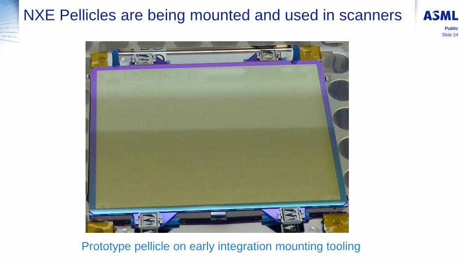
NXE Pellicles are being mounted and used in scanners
Prototype pellicle on early integration mounting tooling

200
400
600
800
1000
1200
1400
0 50 100 150 200 250
Te
mp
era
ture
[C
]
Source power [W]
Maximum pellicle temperature vs
source power (calculated)
Reference (emiss. ≤0.02)
Coated (emiss. 0.24)
Film stackEquivalent
source power
Sample
survivability
Uncoated 40 W 9/9
Uncoated 125 W 3/5
Coated 125 W 33/33
Heat load test results
Pellicle technology: durability proven to at least 125 W
ASML pellicle
integration Work
Center at our
Veldhoven
production
facilities
Public
Slide 25
* Duration of tests: equivalent with exposure of 1000 wafers

EUV source power scaling
Public

Slide 27
Public
EUV Source Architecture, Sn LPP MOPA with Pre-pulse
Source Pedestal
Scanner Pedestal
Fab FloorFab Floor
Sub-fab Floor
Scanner
metrology for
source to
scanner
alignment
CO2 system
Tin catch
Vessel
Vanes
Tin Droplet
Generator
Collector
Beam
Tra
nsp
ort
Power Amplifiers PP&MP Seed unit
Inte
rmed
iate
Fo
cu
s U
nit
xz
Collector
On-droplet Gain Optimization
High Power
Seed System
Laser / EUV dose
Controls
High Power
Amplification Chain
Laser Metrology,
MP PP Focusing

3
12
Slide 28
Public
EUV LPP Source Key Technologies

Slide 29
Public
Source power and availability drive productivity
Productivity = Throughput(EUV Power) Availability
Source power
from 10 W to > 250 W
Drive laser power from 20 to 40 kW
Conversion efficiency (CE) from 1 to 6%
Dose margin from 50 to 10%
Optical transmission
Source availability
Drive laser reliability
Droplet generator reliability & lifetime
Automation
Collector protection
EUV Power= (CO2 laser power CE transmission)*(1-dose overhead)
Raw EUV power
Technology development work is ongoing to improve all aspects
0
20
40
60
80
100
120
140
160
180
200
NOMO and NXE:3100drive laser
MOPA+PP andNXE:3100 drive laser
MOPA+PP andNXE:3300B Drive
Laser
MOPA+PP HighPower Amplification
Chain
Lase
r P
ow
er
(kW
)EU
V P
ow
er
(W)
Do
se O
verh
ead
(%
)
Slide 30
Public
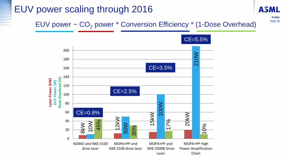
EUV power scaling through 2016
EUV power ~ CO2 power * Conversion Efficiency * (1-Dose Overhead)
CE=0.8%
CE=2.5%
CE=3.5%
CE=5.5%
45%
30% 1
7%
10%1
5kW
12
kW
8kW
10W
50W
100W
20
kW
210W

Pre-pulse technology
Public

Slide 32
Public
Conversion efficiency: Optimizing pre-pulse to create a
more efficient targetTarget expansion fills main pulse beam waist
Prepulse(low energy)
Mainpulse(high energy)
Target shape changes
from droplet to disk

0
1
2
3
4
5
6
7
Slide 33
Public
Increased conversion efficiency with Pre-pulse
no PP small disk large disk partial-cloud cloud
Convers
ion e
ffic
iency (
%)
by optimization of target size, shape and density
EUV CE ~6% demonstrated on development platforms

Slide 34
Public
Plasma scale length (Z) is the key to increase its volume Volume-distributed laser absorption enhances CO2 laser deposition in plasma
Schematic diagram of traditional LPP Hydrodynamic simulation of CO2 Sn LPP
SPIE 2016, 97760K-1, Michael Purvis
“Advances in predictive plasma formation modelling”
laser
n
Te
nc
Corona Energy
transport
Mass flow
Heat, radiation flow
Laser
Laser, e, ions
absorptionablation
EUV
Z
10+
Te Z
ne ni

EUV Source, Drive Laser Development Progress
Public
Slide 36
Public
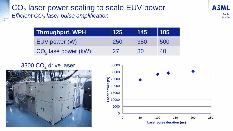
CO2 laser power scaling to scale EUV powerEfficient CO2 laser pulse amplification
3300 CO2 drive laser
Throughput, WPH 125 145 185
EUV power (W) 250 350 500
CO2 lase power (kW) 27 30 40
0
5000
10000
15000
20000
25000
30000
35000
0 50 100 150 200 250
Laser
po
wer
(W)
Laser pulse duration (ns)

Slide 37
Public
CO2 drive laser power scaling
Key technologies:
1. Drive laser with higher power capacity
2. Gain distribution inside amplification chain
3. Mode-matching during beam propagation
4. Isolation between amplifiers
5. Metrology and automation
0
5
10
15
20
25
30
35
40
40 50 60 70 80 90
Po
we
r (k
W)
Repetitation rate (kHz)
0
5000
10000
15000
20000
25000
30000
35000
40000
0 50 100 150 200 250 300 350
PA
s o
utp
ut
(W)
Seed power (W)
PA1
PA2
PA3

Droplet Generator
Public

Slide 39
Public
Droplet Generator, Principle of Operation
• Tin is loaded in a vessel & heated above melting point
• Pressure applied by an inert gas
• Tin flows through a filter prior to the nozzle
• Tin jet is modulated by mechanical vibrations
Nozzle
Filter
ModulatorGas
Sn
0 5 10 15 20 25 30-10
-5
0
5
10
Dro
ple
t p
ositio
n, m
Time, sec
140 m 50 m 30 mPressure: 1005 psi Frequency: 30 kHz Diameter: 37 µm Distance: 1357 µm Velocity: 40.7 m/s
Pressure: 1025 psi Frequency: 50 kHz Diameter: 31 µm Distance: 821 µm Velocity: 41.1 m/s
Pressure: 1025 psi Frequency: 500 kHz Diameter: 14 µm Distance: 82 µm Velocity: 40.8 m/s
Pressure: 1005 psi Frequency: 1706 kHz Diameter: 9 µm Distance: 24 µm Velocity: 41.1 m/s
Fig. 1. Images of tin droplets obtained with a 5.5 μm nozzle. The images on the left were obtained in
frequency modulation regime; the image on the right – with a simple sine wave signal. The images
were taken at 300 mm distance from the nozzle.
Short term droplet position stability σ~1m
16 m

Slide 40
Public
Forces on Droplets during EUV Generation
High EUV power at high repetition rates drives requirements for
higher speed droplets with large space between droplets

Slide 41
Public
High Speed Droplet Generation
Tin droplets at 80 kHz and at different applied pressures.
Images taken at a distance of 200 mm from the nozzle
Pressure (Speed)
3.5 MPa (26 m/s)
6.9 MPa (40 m/s)
13.8 MPa (58 m/s)
27.6 MPa (84 m/s)
41.4 MPa (104 m/s)
55.2 MPa (121 m/s)
1.5 mm

Slide 42
Public
5x improvement in Droplet Generator run time demonstratedData based on ASML internal testing; Field qualification started
Bundle 1 DGen (field avg.)
Bundle II DGen (field avg.)
Bundle III DGen (ASML internal)
Bundle III DGen (Beta Test)
0
100
200
300
400
500
600
700
800
900
1000
2015 Q3 2015 Q4 2016 Q1 2016 Q2
Ru
nti
me
[Ho
urs
]
Field Droplet Generator still
operational >350hrs
Droplet Generator still
operational >1000hrs

EUV Collector, Lifetime
Public

Slide 44
Public
EUV Collector: Normal Incidence
• Ellipsoidal design
• Plasma at first focus
• Power delivered to exposure tool at second focus (intermediate focus)
• 650 mm diameter
• Collection solid angle: 5 sr
• Average reflectivity: > 40%
• Wavelength matching across the entire collection area 5sr Normal Incidence Graded
Multilayer Coated Collector

Slide 45
Public
Collector Protection
Sn droplet /
plasma
H2 flow
Reaction of H radicals with Sn
to form SnH4, which can be
pumped away.
Sn (s) + 4H (g) SnH4 (g)
• Hydrogen buffer gas causes
deceleration of ions
• Hydrogen flow away from collector
reduces atomic tin deposition rate
Laser beam
IF
Sn
catcher
DG
EUV collector
Temperature controlled
• Vessel with vacuum pumping to
remove hot gas and tin vapor
• Internal hardware to collect micro
particles

Slide 46
Public
Collector Lifetime on NXE:3300 SourcesUP2 configuration operating at 60-80W
Transmission loss ~0.5%/Gp
• Collector lifetime ~3 months
(~80Gp) on sources in the field
Transmission loss ~0.6%/Gp
• Customer Demo (Q1’16): >100 Gpulse

Slide 47
Public
250W feasibility proven without increase in protective Hydrogen flowNo rapid collector contamination, allowing stable droplets and >125 w/hr@20 mJ/cm²
~200W dose controlled power

Slide 48
Public
In-situ collector cleaningEffectiveness of product configuration confirmed
Off-line cleaning using NXE:3300B source
vessel with product configuration hardwareReflectivity restored within 0.8% of original
Cleaning in off-line MOPA Prepulse development vessel
Field collector
cleaned in
NXE:3300 source
vessel test rig
Start End
Start End

Slide 49
Public
Summary: EUV readyness for volume manufacturing
• 80% source availability capability demonstrated
• Multiple systems demonstrated >1,000 wafers per day
capability, with one system exceeding 1,350 wpd
• Completed qualification of five NXE:3350B, the 4th generation
EUV exposure tool, one system qualified at 75 wph
• 80W configuration operational in the field, 125W
configuration qualification completed
• Excellent NXE:3350B imaging and overlay
performance at> 80W power
• Continuous progress in resist formulation promising towards
enabling 13nm half pitch at high throughput
• 8 NXE:3300B systems operational at customers

SummarySlide 50
Significant progress in EUV power scaling,
- CE is up to 6 %
- Dose-controlled power is up to 210 W
CO2 developments support EUV power scaling,
- Clean (spatial and temporal) amplification of short CO2 laser pulse
- High power seed-table enables CO2 laser power scaling
Significant progress made in Source Availability
- >80% source availability in the field
- >1000 hrs droplet generator runtime
- >100 Gp collector lifetime
Public

Acknowledgements:Slide 51
Public
David Brandt, Daniel Brown, Rob Rafac, Alexander Schafgans, Yezheng Tao, Michael Purvis, Alex Ershov, Georgiy
Vaschenko, Slava Rokitski, Michael Kats, Daniel Riggs, Wayne Dunstan, Michael Varga, Mathew Abraham, Matthew
Graham
Cymer LLC, 17075 Thornmint Ct, San Diego, CA 92127 USA
Rudy Peeters, Daniel Smith, Uwe Stamm, Sjoerd Lok, Arthur Minnaert, Martijn van Noordenburg, Joerg Mallmann,
David Ockwell, Henk Meijer, Judon Stoeldraijer, Christian Wagner, Carmen Zoldesi, Eelco van Setten, Jo Finders,
Koen de Peuter, Chris de Ruijter, Milos Popadic, Roger Huang, Roderik van Es, Marcel Beckers, Hans Meiling
ASML Netherlands B.V., De Run 6501, 5504 DR Veldhoven, The Netherlands

Acknowledgements:Slide 52
Public