Embed Size (px)
Citation preview
EVAL-AD5696RSDZ User GuideUG-726
One Technology Way • P.O. Box 9106 • Norwood, MA 02062-9106, U.S.A. • Tel: 781.329.4700 • Fax: 781.461.3113 • www.analog.com
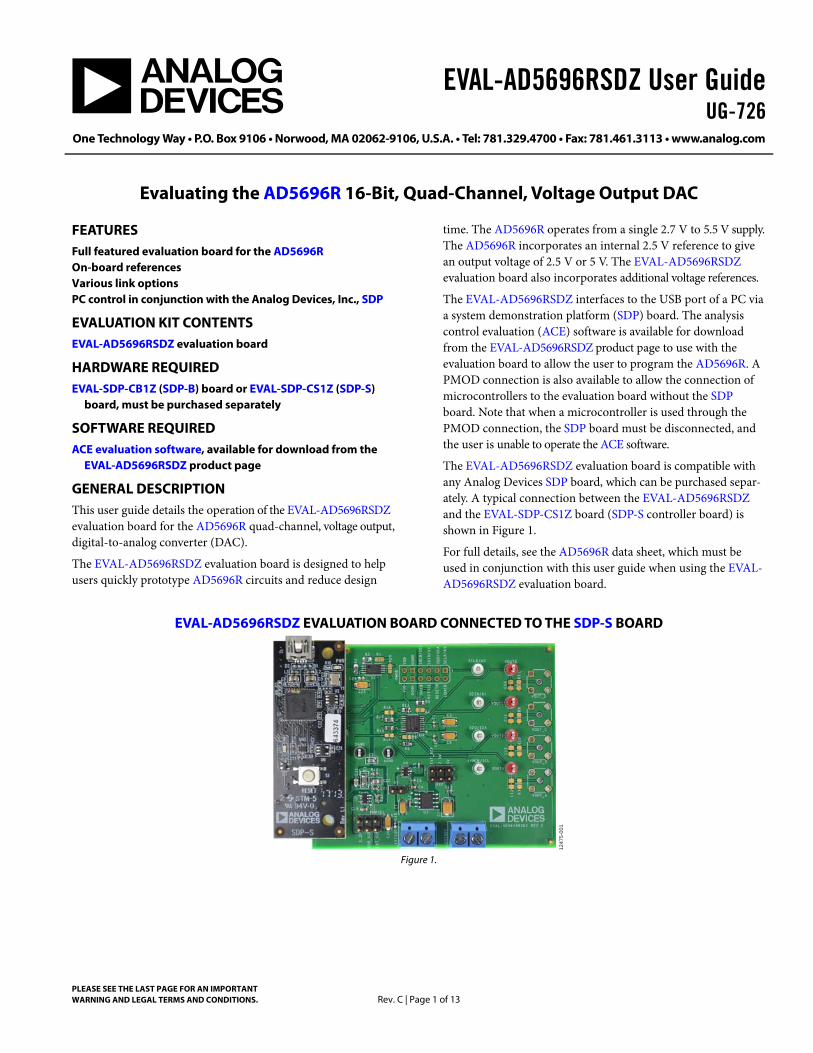
Evaluating the AD5696R 16-Bit, Quad-Channel, Voltage Output DAC
PLEASE SEE THE LAST PAGE FOR AN IMPORTANT WARNING AND LEGAL TERMS AND CONDITIONS. Rev. C | Page 1 of 13
FEATURES Full featured evaluation board for the AD5696R On-board references Various link options PC control in conjunction with the Analog Devices, Inc., SDP
EVALUATION KIT CONTENTS EVAL-AD5696RSDZ evaluation board
HARDWARE REQUIRED EVAL-SDP-CB1Z (SDP-B) board or EVAL-SDP-CS1Z (SDP-S)
board, must be purchased separately
SOFTWARE REQUIRED ACE evaluation software, available for download from the
EVAL-AD5696RSDZ product page
GENERAL DESCRIPTION This user guide details the operation of the EVAL-AD5696RSDZ evaluation board for the AD5696R quad-channel, voltage output, digital-to-analog converter (DAC).
The EVAL-AD5696RSDZ evaluation board is designed to help users quickly prototype AD5696R circuits and reduce design
time. The AD5696R operates from a single 2.7 V to 5.5 V supply. The AD5696R incorporates an internal 2.5 V reference to give an output voltage of 2.5 V or 5 V. The EVAL-AD5696RSDZ evaluation board also incorporates additional voltage references.
The EVAL-AD5696RSDZ interfaces to the USB port of a PC via a system demonstration platform (SDP) board. The analysis control evaluation (ACE) software is available for download from the EVAL-AD5696RSDZ product page to use with the evaluation board to allow the user to program the AD5696R. A PMOD connection is also available to allow the connection of microcontrollers to the evaluation board without the SDP board. Note that when a microcontroller is used through the PMOD connection, the SDP board must be disconnected, and the user is unable to operate the ACE software.
The EVAL-AD5696RSDZ evaluation board is compatible with any Analog Devices SDP board, which can be purchased separ-ately. A typical connection between the EVAL-AD5696RSDZ and the EVAL-SDP-CS1Z board (SDP-S controller board) is shown in Figure 1.
For full details, see the AD5696R data sheet, which must be used in conjunction with this user guide when using the EVAL-AD5696RSDZ evaluation board.
EVAL-AD5696RSDZ EVALUATION BOARD CONNECTED TO THE SDP-S BOARD
1247
5-00
1
Figure 1.

UG-726 EVAL-AD5696RSDZ User Guide
Rev. C | Page 2 of 13
TABLE OF CONTENTS Features .............................................................................................. 1 Evaluation Kit Contents ................................................................... 1 Hardware Required .......................................................................... 1 Software Required ............................................................................ 1 General Description ......................................................................... 1 EVAL-AD5696RSDZ Evaluation Board Connected to the SDP-S Board ...................................................................................... 1 Revision History ............................................................................... 2 Evaluation Board Software Quick Start Procedures .................... 3
Installing the Software ................................................................. 3 Initial Setup ................................................................................... 3
Block Diagram and Description ......................................................4 Memory Map .................................................................................5
Evaluation Board Hardware .............................................................6 Power Supplies ...............................................................................6 LDO Recommendation ................................................................6 Test Points ......................................................................................6 Voltage References.........................................................................6 Link Options ..................................................................................6
Evaluation Board Schematics and Artwork ...................................8 Ordering Information .................................................................... 12
Bill of Materials ........................................................................... 12
REVISION HISTORY 6/2017—Rev. B to Rev. CChange to Features Section ............................................................. 1
4/2017—Rev. A to Rev. B Reorganized Layout ............................................................ Universal Changes to Evaluation Kit Contents Section and General Description Section .......................................................................... 1 Added Hardware Required Section and Software Required Section ................................................................................................ 1 Added Evaluation Board Software Quick Start Procedures Section, Installing the Software Section, Initial Setup Section, Figure 2, and Figure 3; Renumbered Sequentially ....................... 3 Added Block Diagram and Description Section, Figure 4, and Table 1; Renumbered Sequentially.......................................... 4 Deleted Evaluation Board Software Section, Installing the Software Section, Running the Software Section, Figure 2, Figure 3, Figure 4, and Figure 5; Renumbered Sequentially ....... 5 Added Memory Map Section, Figure 5, and Figure 6 ................. 5 Deleted Figure 6, Software Operation Section, Write to Input Register Section, Write to DAC Register Section, Update DAC Register from Input Register Section, LDAC Control
Section, GAIN Control Section, Reference Control Section, and Power-Down Control Section .................................................. 6 Changes to Table 2 ............................................................................. 6 Deleted LDAC Mask Register Section and 24-Bit Command Section ................................................................................................. 7 Changes to Table 6 .......................................................................... 12
2/2016—Rev. 0 to Rev. A Changes to Table 4 ............................................................................. 4 Changes to Running the Software Section ..................................... 5 Added Figure 5; Renumbered Sequentially ................................... 5 Changes to Figure 6 ........................................................................... 6 Added LDAC Mask Register Section .............................................. 7 Changes to Figure 7 ........................................................................... 8 Changes to Figure 8 ........................................................................... 9 Changes to Figure 9 and Figure 10 ............................................... 10 Changes to Figure 11 ...................................................................... 11 Changes to Table 5 .......................................................................... 12
5/2015—Revision 0: Initial Version

EVAL-AD5696RSDZ User Guide UG-726
Rev. C | Page 3 of 13
EVALUATION BOARD SOFTWARE QUICK START PROCEDURES INSTALLING THE SOFTWARE The EVAL-AD5696RSDZ evaluation board uses the ACE evaluation software, a desktop software application that allows the evaluation and control of multiple evaluation systems.
The ACE installer installs the necessary SDP drivers and the Microsoft® .NET Framework 4 by default. The ACE software is available for download from the EVAL-AD5696RSDZ product page, and must be installed before connecting the SDP board to the USB port of the PC, to ensure that the SDP board is recognized when it connects to the PC. For full instructions on how to install and use this software, see the ACE software page on the Analog Devices website.
After the installation is finished, the EVAL-AD5696RSDZ evaluation board plug in appears when the ACE software is opened.
INITIAL SETUP To set up the evaluation board, take the following steps:
1. Connect the evaluation board to the SDP board, and thenconnect the USB cable between the SDP board and the PC.
2. Run the ACE application. The EVAL-AD5696RSDZ boardplug ins appear in the attached hardware pane of the Starttab.
3. Double click the board plug in to open the board viewshown in Figure 2.
4. Double click the AD5696R chip to access the chip blockdiagram. This view provides a basic representation offunctionality of the board. The main function blocks of theboard are labeled in Figure 3.
1247
5-10
2
Figure 2. Board View of the EVAL-AD5696RSDZ
1247
5-10
3
Figure 3. Chip Block Diagram of the AD5696R

UG-726 EVAL-AD5696RSDZ User Guide
Rev. C | Page 4 of 13
BLOCK DIAGRAM AND DESCRIPTION The EVAL-AD5696RSDZ software is organized to appear similar to the functional block diagram shown in the AD5696R data sheet. Therefore, correlating the functions on the EVAL-AD5696RSDZ evaluation board with the description in the AD5696R data sheet is simplified.
For a full description of each block, register, and its settings, see the AD5696R data sheet.
Some of the blocks and their functions are described in this section as they pertain to the evaluation board. The block diagram is shown in Figure 4. Table 1 describes the functionality of each block.
1247
5-10
4
J
A C I
B F D G E H Figure 4. AD5696R Block Diagram with Labels
Table 1. Block Diagram Functions (See Figure 4 for Labels) Label Button/Function Name Function A CONFIGURATION
wizard Used to set the initial configuration for the board. Select the reference gain case from the Output Gain dropdown menu. A gain of 1 is the default. After setting up the initial configuration, click Apply to apply the values. These settings can be modified at any stage while evaluating the board.
B LDAC and RESET (GPIO buttons)
Act as external GPIO pulses to the LDAC and RESET pins. The LDAC button transfers data from the input registers (D) to the DAC registers (E). The RESET button clears all data from input registers and DAC registers. These buttons are live; therefore, there is no need to click Apply Changes (J).
C Select a Command Command option dropdown menu selects how the data being transferred to the device affects the input and DAC registers. After a data value is entered in an input register (D), this menu determines the internal DAC registers affected by updating the input register (D). After a new value is written in the input register (D), the data can be transferred to the DAC input register, or to the DAC input register and the DAC register simultaneously. If the data is transferred to both registers, the channel DAC register (E) will reflect the new value.
D Input register 16-bit data word to be transferred to the device. Click Apply Changes (J) to transfer this 16-bit data word to the device.
E DAC register Displays the value that is currently present in the DAC register on the device. Update the DAC registers by selecting the appropriate command option or by toggling LDAC (B).
F Software RESET Returns the evaluation board and software to default values. This button is live; therefore, there is no need to click Apply Changes (J).
G Load DAC Users can individually control which channel loads the values from the input registers to the DAC registers.
H DAC DAC configuration options provide access to individual channel configuration options such as power-down options and hardware LDAC mask enable/disable settings.
I Internal Reference Select Enable from this setting to enable the on-chip reference for the evaluation board. If Disable is selected, an external reference must be applied. This control is only available on the AD5696R.
J Apply Changes Applies all modified values to the device. Note that if an evaluation board is not connected, values entered into the input registers are not transferred to the DAC registers.

EVAL-AD5696RSDZ User Guide UG-726
Rev. C | Page 5 of 13
MEMORY MAP All registers are fully accessible from the AD5696R Memory Map tab, shown in Figure 5. To navigate to this tab, click the Proceed to Memory Map button, shown in Figure 4. This tab allows registers to be edited at bit level. The bits shaded in dark gray are read-only bits and cannot be accessed from the ACE software. All other bits are toggled.
Clicking the Apply Changes button transfers data to the device. All changes made in the memory map tab correspond to the block diagram. For example, if the internal register bit is enabled, it displays as enabled on the block diagram. Any bits or registers that are shown in bold in the memory map tab are modified values that have not been transferred to the evaluation board (see Figure 6). Click Apply Changes to transfer the data to the evaluation board.
1247
5-10
5
Figure 5. AD5696R Memory Map Tab
1247
5-10
6
Figure 6. AD5696R Memory Map with Unapplied Changes in the
DAC0_Input Register

UG-726 EVAL-AD5696RSDZ User Guide
Rev. C | Page 6 of 13
EVALUATION BOARD HARDWARE POWER SUPPLIES The EVAL-AD5696RSDZ evaluation board provides an on-board, 3.3 V regulator powered through the USB supply. If a different supply is required or if the evaluation board is controlled through the PMOD connector, an external supply must be provided by the EXTSUP connector. See Table 2 for more details.
Both AGND and DGND inputs are provided on the board. The AGND and DGND planes are connected at one location close to the AD5696R. To avoid ground loop problems, it is recommended that AGND and DGND not be connected elsewhere in the system.
All supplies are decoupled to ground with 10 µF tantalum and 0.1 µF ceramic capacitors.
LDO RECOMMENDATION The ADP7118 low dropout (LDO) linear regulator (maximum VIN = 20 V) is recommended to power the VDD rail for maximal performance. A 4.7 Ω resistor in series with the input capacitor of the ADP7118 adds additional rejection at higher frequencies to reduce any power supply ripple artifacts below the noise floor. The ADP162 is recommended for powering the VLOGIC rail.
TEST POINTS The evaluation board has various test points for debugging and monitoring purposes. These test points are described Table 5.
VOLTAGE REFERENCES The AD5696R provides an internal voltage reference. The evaluation board provides external references with values of 2.5 V and 5 V. Note that the ADR3450 requires the use of an external supply through the EXTSUP connector (see Table 4).
LINK OPTIONS A number of link options are incorporated on the EVAL-AD5696RSDZ evaluation board and must be set for the required operating conditions before using the board. The functions of these link options are described in Table 4.
Table 3 lists the positions of the different links controlled by the PC via the USB port. An SDP board operating in single-supply mode is required.
Table 2. Power Supply Connectors Connector No. Label External Voltage Supplies Description EXTSUP, Pin 1 EXTSUP External analog power supply from 2.7 V to 5.5 V, VDD. EXTSUP, Pin 2 Analog ground. EXTREF, Pin 1 EXTREF External voltage reference, VLOGIC. 3.3 V when the evaluation board is controlled through the SDP. 1.8 V to 5.5 V when the evaluation board is controlled through an external connector. EXTREF, Pin 2 Analog ground.
Table 3. Link Options Setup for SDP Control (Default) Link Option PWRSEL 3.3 V REF Not connected P1 Not connected
Table 4. Link Functions Link Description PWRSEL This link selects the DAC analog voltage source. There are three options as follows: The 3.3 V option selects the on-board voltage source from the ADP121. The USB_SUP option selects the USB supply from Pin 5 of the 120-pin connector of the SDP board. The EXT_SUP option selects an external supply voltage (EXTSUP connector). REF This link selects the reference source. There are four options as follows: The not connected option uses the internal reference of 2.5 V. The EXT_REF option selects an external reference source (EXTREF connector). The 2.5 V option selects the on-board reference from the REF192. The 5 V option selects the on-board reference from the ADR3450. This reference requires an external supply. P1 The P1 link selects the DAC digital voltage source. There are two options as follows: The connected option shorts VDD and VLOGIC. Use this option only when the SDP is not connected. The not connected option opens the connection of VDD and VLOGIC. Use this option when using the SDP.

EVAL-AD5696RSDZ User Guide UG-726
Rev. C | Page 7 of 13
Table 5. Test Point Descriptions Test Point Description AGND Analog ground. DGND Digital ground. SCLK/A0 Address input. Sets the first LSB of the 7-bit slave address. This signal is named SCLK_A0 in Figure 7. SDO/SDA Serial data line. This pin is used in conjunction with the SCL line to clock data into or out of the 24-bit input shift
register. SDA is a bidirectional, open-drain data line pulled to the supply with an external pull-up resistor. This signal is named SDO_SDA in Figure 7. If using an external microcontroller, a 2.2 kΩ pull-up resistor connected to VLOGIC is required.
SYNCB/SCL Serial clock line. This pin is used in conjunction with the SDA line to clock data into or out of the 24-bit input register. This signal is named SYNCB_SCL in Figure 7. If an external microcontroller is used, a 2.2 kΩ pull-up resistor connected to VLOGIC is required.
SDIN/A1 Address input. This pin sets the second LSB of the 7-bit slave address. This signal is named SDIN_A1 in Figure 7. VOUTA to VOUTD Analog output voltage from DAC A to DAC D, respectively. The output amplifier has rail-to-rail operation.
UG-726 EVAL-AD5696RSDZ User Guide
Rev. C | Page 8 of 13
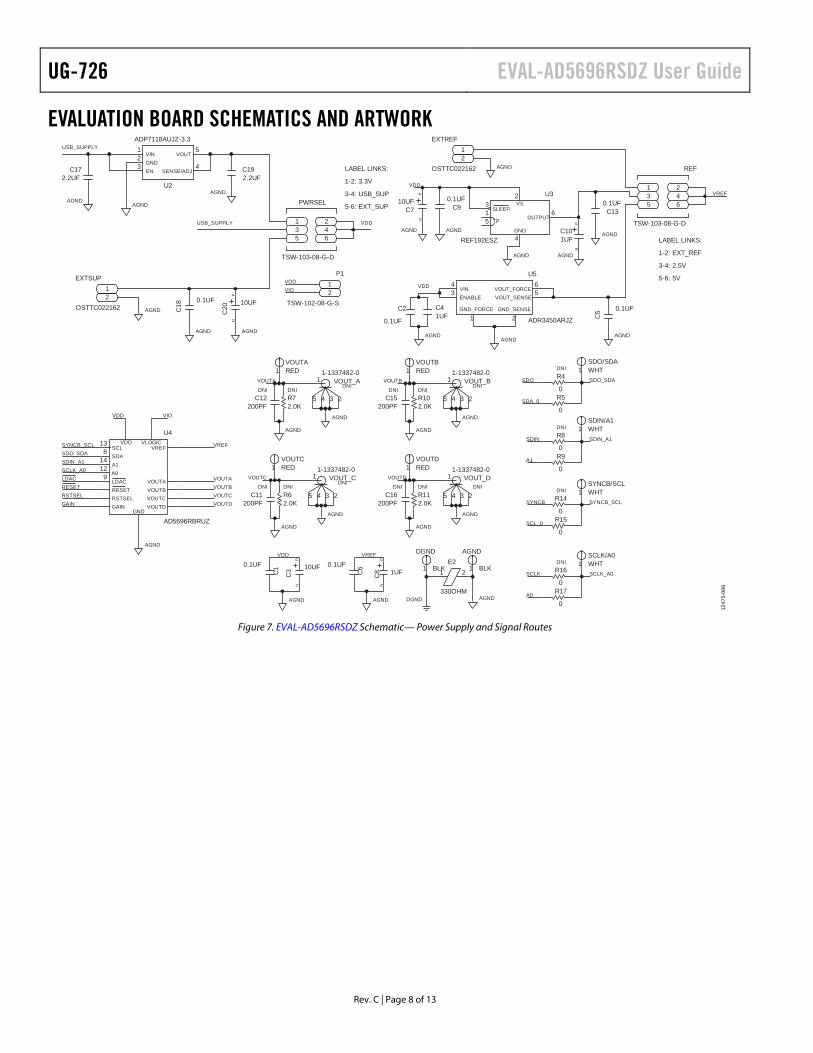
EVALUATION BOARD SCHEMATICS AND ARTWORK
1247
5-00
6
VOUT_D1-1337482-0
2.0K2
DNIC11
200PF
1
5
1VOUTA
DNIDNI
200PF
1-1337482-0 REDVOUT_C
VOUTC
3
DNI
200PF 2.0K
5
VOUT_B1-1337482-0
3 4 2
1VOUTD
C16 R11
4 3 2
11
VOUTB
C15 R10
R6
1
5 4 2
1
VOUTA
R7C12 5 4 3
1 VOUT_A
REDVOUTC
DNI DNI
VOUTB
200PF
RED
DNI
2.0K
DNI
RED
2.0K
1-1337482-0
DNI
VOUTD
DNI
DNIDNI
AGND
AGND
AGND
AGND
AGND
AGND
AGND
AGND
NP
0.1UFVREF
C8C6
C3
0.1UFVDD
10UF
PN
1UFC1
AGNDAGND
1
AGND
21E2
1
DGND
330OHM
BLK BLK
DGND AGND
0
SYNCB/SCL
SCLK_A0
SCLK/A0
SYNCB_SCL
SDIN/A1DNI
R161
1
1
1SDO/SDA
R15
R14
R17
R9
R4
R5
R8
0
SDO
0
A0
0
0
DNI
SCLK
SYNCB
WHTSDIN
WHT
0
A1
DNI
SDA_0
0
DNI
SDIN_A1
SDO_SDA
WHT
WHT
0SCL_0AD5696RBRUZ
GAIN
VOUTA
813
9
1412
U4
VDD VIO
SCLK_A0SDIN_A1
RSTSEL
VREF
VOUTCVOUTB
VOUTD
SDO_SDASYNCB_SCL
AGND
VOUTB
VREF
RSTSELRESET
A1
SCL
A0
VLOGIC
GAIN
LDAC
SDA
VOUTDVOUTC
VDD
GND
VOUTA
21
P1VDDVIO
TSW-102-08-G-S
5-6: EXT_SUP
LABEL LINKS:
1-2: 3.3V
3-4: USB_SUP
4
5123
U2
C17 C19
654321
PWRSEL
C18
21
EXTSUP
NP
C20
10UF0.1UF
TSW-103-08-G-D
VDD
OSTTC022162
USB_SUPPLY
USB_SUPPLY
2.2UF
ADP7118AUJZ-3.3
2.2UF
VOUT
SENSE/ADJENGNDVIN
AGNDAGND
AGND
AGNDAGND
AGND
LABEL LINKS:
1-2: EXT_REF
5-6: 5V
3-4: 2.5V
NP
C10
C13C9
NP
C7
C4
C5C2
654321
REF
564
21
3
U5
21
EXTREF
2
513
6
4
U310UF 0.1UF0.1UF
0.1UF
0.1UF
VDD
ADR3450ARJZ
VDD
1UF
VREF
REF192ESZ
TSW-103-08-G-D
1UF
OSTTC022162
AGNDAGND
AGNDAGNDAGND
VOUT_FORCEVOUT_SENSE
VINENABLE
GND_SENSEGND_FORCE
AGND
AGND
SLEEPVS
OUTPUT
GND
TP
AGND
AGND
RESETLDAC
Figure 7. EVAL-AD5696RSDZ Schematic— Power Supply and Signal Routes

EVAL-AD5696RSDZ User Guide UG-726
Rev. C | Page 9 of 13
1247
5-00
7
IF VCC WILL BE USED TO POWER THE MODULE, PROVIDE PROTECTION CIRCUIT BLOCK IF POSSIBLE
CONNECT VCC TO 3.3V DIGITAL REFERENCE OR LEAVE FLOATING
CONNECT P1-P4 AND P7-P10 TO SIGNAL BUSES FOR SPI
PMOD INTERFACE TYPE 2A (EXPANDED SPI)
SYNCB_SCL
SDIN_A1
LDACB
DNI
SCLK_A0
SDO_SDA
GAIN
RESETB
RSTSEL
TSW-106-08-G-DVIOVDD
PMOD
5 11
1234
78910
6 12VCCGNDP10
P9P8P7
VCCGNDP4P3P2P1
DGND DGND
HIGH OR LOW BY YOUR BOARD AT POWER UP. FAILURE TO MEET THIS
AN ACTIVE LOW CHIP SELECT. ENSURE ALSO THAT THE SPI CLK LINE IS NOT HELD
IS NOT ACTIVELY DRIVING THE MISO DATA LINE UNLESS PROPERLY ADDRESSED WITH
SINCE SPI IS A SHARED BUS, ENSURE THAT ANY SPI DEVICE ON DAUGHTER BOARD
ON THE SPI_SEL_A/B/C LINES THAT ARE ACTIVE LOW ENABLED
WHEN USING SPI INTERFACE, BE AWARE OF ADDING A PULL UP
THE SDP REQUIRES 5V 300MA
MAIN 12C BUS (CONNECTED TO BLACKFIN TWI - PULL UP RESISTORS NOT REQUIRED
SPI_SEL1/SPI_SS MUST BE ONLY USED
GPIO - USE 12C_0 FIRST)
REQUIRED (CONNECTED TO BLACKFIN
CONNECTORS ON SDP - PULL UP RESISTORS
THE SDP CONNECTOR IMPLEMENTS THE E13 CONNECTOR SPECIFICATIONS STANDARD. THIS IS A STANDARD FOR USE ACROSS ADI AND CANNOT BE MODIFIED
12C BUS 1 IS COMMON ACROSS BOTH
VIO: USE TO SET IO VOLTAGE MAX DRAW 20MA
: USE ONLY TO POWER THE EEPROM(3MA MAX DRAW)
VIN: USE THIS PIN TO POWER
BOARD ID EEPROM (24LC32) MUST BE ON I2C BUS 0
WITH EXTERNAL SPI FLASH
TO BOOT FROM A SPI FLASH ON THE DAUGHTER BOARD
BMODE1: PULL UP WITH A 10K RESISTOR TO SET SDP
RESULT TO A NON-FUNCTIONAL SYSTEM.
114
6952
SDP CONNECTOR
R20
SCLK
100
R13
118119
FX8-120S-SV(21)
C22
1.8
2E1
107108109
10UF600OHM
SDA_0
R0603
DNI
100KR0603
SDIN
R0603
TOL=1
100K
DNI
SDO
SCL_0
RSTSEL
LDACB
A1A0
RESETB
GAIN
TOL=1
100K
TOL=1
R0603100K
VIO
0VIO
USB_SUPPLY
EEPROM
24LC32A-I/ST
10UF
TSSOP8
0.1UF
SYNCB
VIO
0.1UF4.7UF
SDP61
71
56
34
6
11
17
23
28
36
40
46
58 63
75
81
86
93
98
104
115
117
43 7844 7745 76
47 74
2
5051
535455 66
6768
70
120
96259724
94
22
101201021910318
1051610615
141312
1101111011291138
7
279526
9921
60
57
79428041
35
64
82
3334
8384
39
853738
9131
8832
90
922930
89
87
48 7349 72
59 62
5
1
116
65
U11236
5
8
4
7
R2
R3
R1C25C24
PN
R12
C21 C23
1
DGND
DGNDDGND
DGND
AGND AGND
VSS
VCC
WP
A2A1A0
SCLSDA
DGND
DGND
DGND
SPI_SEL_A
CLKOUT
NCNC
GNDGND
VIO(+3.3V)GND
PAR_D22PAR_D20PAR_D18PAR_D16PAR_D15
GNDPAR_D12PAR_D10
PAR_D8PAR_D6
GNDPAR_D4PAR_D2PAR_D0
PAR_WR_NPAR_INT
GNDPAR_A2PAR_A0
PAR_FS2PAR_CLK
GNDSPORT_RSCLK
SPORT_DR0SPORT_RFSSPORT_TFSSPORT_DT0
SPORT_TSCLKGND
SPI_MOSISPI_MISO
SPI_CLKGND
SDA_0SCL_0GPIO1GPIO3GPIO5
GNDGPIO7
TMR_BTMR_D
NCGND
NCNCNC
WAKE_NSLEEP_N
GNDUART_TXBMODE1RESET_IN_N
UART_RXGNDRESET_OUT_NEEPROM_A0NCNCNCGNDNCNCTMR_CTMR_AGPIO6GNDGPIO4GPIO2GPIO0SCL_1SDA_1GNDSPI_SEL1/SPI_SS_NSPI_SEL_C_NSPI_SEL_B_NGNDSERIAL_INTSPI_D3SPI_D2SPORT_DT1SPORT_DR1SPORT_TDV1SPORT_TDV0GNDPAR_FS1PAR_FS3PAR_A1PAR_A3GNDPAR_CS_NPAR_RD_NPAR_D1PAR_D3PAR_D5GNDPAR_D7PAR_D9PAR_D11PAR_D13PAR_D14GNDPAR_D17PAR_D19PAR_D21PAR_D23GNDUSB_VBUSGNDGNDNCVIN
Figure 8. EVAL-AD5696RSDZ Schematic—SDP Connector

UG-726 EVAL-AD5696RSDZ User Guide
Rev. C | Page 10 of 13
1247
5-00
8
Figure 9. EVAL-AD5696RSDZ Component Placement
1247
5-00
9
Figure 10. EVAL-AD5696RSDZ Top Side Routing

EVAL-AD5696RSDZ User Guide UG-726
Rev. C | Page 11 of 13
1247
5-01
0
Figure 11. EVAL-AD5696RSDZ Bottom Side Routing

UG-726 EVAL-AD5696RSDZ User Guide
Rev. C | Page 12 of 13
ORDERING INFORMATION BILL OF MATERIALS
Table 6. Qty Reference Designator Description Supplier/Part Number1, 2 1 U1 32 kΩ, I2C serial EEPROM (24LC32) FEC/1331330 1 U2 150 mA, low quiescent current, CMOS linear regulator Analog Devices/ADP121 1 U3 2.5 V precision micropower, low dropout, low voltage reference Analog Devices/REF192 1 U4 Quad, 16-bit nanoDAC+ with 2 ppm/°C on-chip reference and I2C
interface Analog Devices/AD5696R
1 U5 Micropower, high accuracy, 5.0 V voltage reference Analog Devices/ADR3450 6 C1, C2, C5, C6, C18, C25 Capacitor, 0.1 µF, 16 V, 0402 Generic 3 C4, C17, C19 Capacitor, 1 µF, 25 V, X5R Generic 3 C3, C20, C24 Capacitor, 10 µF, 10 V, tantalum Generic 1 C8 Capacitor, 1 µF, 16 V, tantalum Generic 1 C21 Capacitor, 10 µF, 25 V, X5R Generic 1 C22 Capacitor, 4.7 µF, 25 V, X5R Generic 1 C23 Capacitor, 0.1 µF, 25 V, X8R Generic 1 E1 Ferrite bead, 600 Ω Generic 1 E2 Ferrite bead, 330 Ω Generic 2 EXTREF, EXTSUP 2-pin terminal block Generic 1 P1 2-pin link/jumper Generic 2 REF, PWRSEL 6-pin link/jumper Generic 1 R12 Resistor, 1.8 Ω, 5%, 1/10 W, thick film chip Generic 1 R13 Resistor, 0 Ω, SMD Generic 4 R5, R9, R15, R17 Resistor, 0 Ω, 5%, 1/16 W, 0603 Generic 2 R2, R3 Resistor, 100 kΩ, 1%, 1/10 W Generic 1 SDP 120-pin female connector FEC/1324660 or Digi-Key/H1219-ND 2 AGND, DGND Black test point Generic 4 SCLK/A0, SDIN/A1,
SDO/SDA, SYNCB/SCL White test point Generic
4 VOUTA to VOUTD Red test point Generic 19 PMOD, C11, C12, C15,
C16, R1, R4, R6 to R8, R10, R11, R14, R16, R20, VOUT_A to VOUT_D
Do not insert/do not populate Not inserted
1 FEC refers to Farnell Electronic Component Distributors. 2 Generic indicates that any device with the specified value, size, and rating can be used.
EVAL-AD5696RSDZ User Guide UG-726
Rev. C | Page 13 of 13
NOTES
I2C refers to a communications protocol originally developed by Philips Semiconductors (now NXP Semiconductors).
ESD Caution ESD (electrostatic discharge) sensitive device. Charged devices and circuit boards can discharge without detection. Although this product features patented or proprietary protection circuitry, damage may occur on devices subjected to high energy ESD. Therefore, proper ESD precautions should be taken to avoid performance degradation or loss of functionality.
Legal Terms and Conditions By using the evaluation board discussed herein (together with any tools, components documentation or support materials, the “Evaluation Board”), you are agreeing to be bound by the terms and conditions set forth below (“Agreement”) unless you have purchased the Evaluation Board, in which case the Analog Devices Standard Terms and Conditions of Sale shall govern. Do not use the Evaluation Board until you have read and agreed to the Agreement. Your use of the Evaluation Board shall signify your acceptance of the Agreement. This Agreement is made by and between you (“Customer”) and Analog Devices, Inc. (“ADI”), with its principal place of business at One Technology Way, Norwood, MA 02062, USA. Subject to the terms and conditions of the Agreement, ADI hereby grants to Customer a free, limited, personal, temporary, non-exclusive, non-sublicensable, non-transferable license to use the Evaluation Board FOR EVALUATION PURPOSES ONLY. Customer understands and agrees that the Evaluation Board is provided for the sole and exclusive purpose referenced above, and agrees not to use the Evaluation Board for any other purpose. Furthermore, the license granted is expressly made subject to the following additional limitations: Customer shall not (i) rent, lease, display, sell, transfer, assign, sublicense, or distribute the Evaluation Board; and (ii) permit any Third Party to access the Evaluation Board. As used herein, the term “Third Party” includes any entity other than ADI, Customer, their employees, affiliates and in-house consultants. The Evaluation Board is NOT sold to Customer; all rights not expressly granted herein, including ownership of the Evaluation Board, are reserved by ADI. CONFIDENTIALITY. This Agreement and the Evaluation Board shall all be considered the confidential and proprietary information of ADI. Customer may not disclose or transfer any portion of the Evaluation Board to any other party for any reason. Upon discontinuation of use of the Evaluation Board or termination of this Agreement, Customer agrees to promptly return the Evaluation Board to ADI. ADDITIONAL RESTRICTIONS. Customer may not disassemble, decompile or reverse engineer chips on the Evaluation Board. Customer shall inform ADI of any occurred damages or any modifications or alterations it makes to the Evaluation Board, including but not limited to soldering or any other activity that affects the material content of the Evaluation Board. Modifications to the Evaluation Board must comply with applicable law, including but not limited to the RoHS Directive. TERMINATION. ADI may terminate this Agreement at any time upon giving written notice to Customer. Customer agrees to return to ADI the Evaluation Board at that time. LIMITATION OF LIABILITY. THE EVALUATION BOARD PROVIDED HEREUNDER IS PROVIDED “AS IS” AND ADI MAKES NO WARRANTIES OR REPRESENTATIONS OF ANY KIND WITH RESPECT TO IT. ADI SPECIFICALLY DISCLAIMS ANY REPRESENTATIONS, ENDORSEMENTS, GUARANTEES, OR WARRANTIES, EXPRESS OR IMPLIED, RELATED TO THE EVALUATION BOARD INCLUDING, BUT NOT LIMITED TO, THE IMPLIED WARRANTY OF MERCHANTABILITY, TITLE, FITNESS FOR A PARTICULAR PURPOSE OR NONINFRINGEMENT OF INTELLECTUAL PROPERTY RIGHTS. IN NO EVENT WILL ADI AND ITS LICENSORS BE LIABLE FOR ANY INCIDENTAL, SPECIAL, INDIRECT, OR CONSEQUENTIAL DAMAGES RESULTING FROM CUSTOMER’S POSSESSION OR USE OF THE EVALUATION BOARD, INCLUDING BUT NOT LIMITED TO LOST PROFITS, DELAY COSTS, LABOR COSTS OR LOSS OF GOODWILL. ADI’S TOTAL LIABILITY FROM ANY AND ALL CAUSES SHALL BE LIMITED TO THE AMOUNT OF ONE HUNDRED US DOLLARS ($100.00). EXPORT. Customer agrees that it will not directly or indirectly export the Evaluation Board to another country, and that it will comply with all applicable United States federal laws and regulations relating to exports. GOVERNING LAW. This Agreement shall be governed by and construed in accordance with the substantive laws of the Commonwealth of Massachusetts (excluding conflict of law rules). Any legal action regarding this Agreement will be heard in the state or federal courts having jurisdiction in Suffolk County, Massachusetts, and Customer hereby submits to the personal jurisdiction and venue of such courts. The United Nations Convention on Contracts for the International Sale of Goods shall not apply to this Agreement and is expressly disclaimed.
©2015–2017 Analog Devices, Inc. All rights reserved. Trademarks and registered trademarks are the property of their respective owners. UG12475-0-6/17(C)