Embed Size (px)
Citation preview
Evaluation Board User Guide UG-456
One Technology Way • P.O. Box 9106 • Norwood, MA 02062-9106, U.S.A. • Tel: 781.329.4700 • Fax: 781.461.3113 • www.analog.com
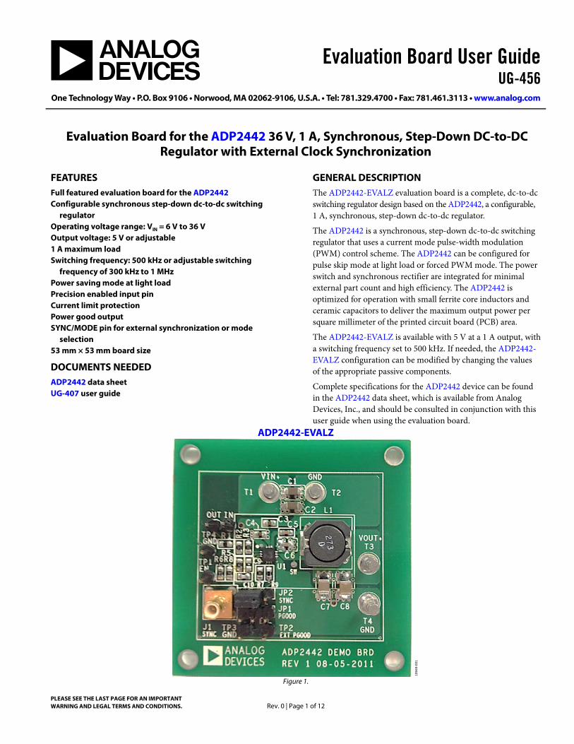
Evaluation Board for the ADP2442 36 V, 1 A, Synchronous, Step-Down DC-to-DC
Regulator with External Clock Synchronization
PLEASE SEE THE LAST PAGE FOR AN IMPORTANT WARNING AND LEGAL TERMS AND CONDITIONS. Rev. 0 | Page 1 of 12
FEATURES Full featured evaluation board for the ADP2442 Configurable synchronous step-down dc-to-dc switching
regulator Operating voltage range: VIN = 6 V to 36 V Output voltage: 5 V or adjustable 1 A maximum load Switching frequency: 500 kHz or adjustable switching
frequency of 300 kHz to 1 MHz Power saving mode at light load Precision enabled input pin Current limit protection Power good output SYNC/MODE pin for external synchronization or mode
selection 53 mm × 53 mm board size
DOCUMENTS NEEDED ADP2442 data sheet UG-407 user guide
GENERAL DESCRIPTION The ADP2442-EVALZ evaluation board is a complete, dc-to-dc switching regulator design based on the ADP2442, a configurable, 1 A, synchronous, step-down dc-to-dc regulator.
The ADP2442 is a synchronous, step-down dc-to-dc switching regulator that uses a current mode pulse-width modulation (PWM) control scheme. The ADP2442 can be configured for pulse skip mode at light load or forced PWM mode. The power switch and synchronous rectifier are integrated for minimal external part count and high efficiency. The ADP2442 is optimized for operation with small ferrite core inductors and ceramic capacitors to deliver the maximum output power per square millimeter of the printed circuit board (PCB) area.
The ADP2442-EVALZ is available with 5 V at a 1 A output, with a switching frequency set to 500 kHz. If needed, the ADP2442-EVALZ configuration can be modified by changing the values of the appropriate passive components.
Complete specifications for the ADP2442 device can be found in the ADP2442 data sheet, which is available from Analog Devices, Inc., and should be consulted in conjunction with this user guide when using the evaluation board.
ADP2442-EVALZ
Figure 1.
1094
9-00
1
UG-456 Evaluation Board User Guide
Rev. 0 | Page 2 of 12
TABLE OF CONTENTS Features .............................................................................................. 1 Documents Needed .......................................................................... 1 General Description ......................................................................... 1 ADP2442-EVALZ ............................................................................. 1 Revision History ............................................................................... 2 Using the Evaluation Board ............................................................. 3
Powering Up the Evaluation Board ............................................ 3 Measuring Evaluation Board Performance .................................. 4
Modifying the Evaluation Board .....................................................5 Changing the Output Voltage ......................................................5 Changing the Switching Frequency ............................................5
Typical Performance Characteristics ..............................................6 Evaluation Board Schematic and Artwork .....................................8 Ordering Information .................................................................... 10
Bill of Materials ........................................................................... 10
REVISION HISTORY 11/12—Revision 0: Initial Version

Evaluation Board User Guide UG-456
Rev. 0 | Page 3 of 12
USING THE EVALUATION BOARD POWERING UP THE EVALUATION BOARD The ADP2442-EVALZ evaluation board is provided fully assembled and tested. Before applying power to the evaluation board, follow the procedures in the following sections.
Input Power Source
The power source voltage must not exceed 36 V, the maximum operation input voltage of the ADP2442.
Ensure that the power source is switched off before connecting it to the ADP2442-EVALZ evaluation board. Connect the positive terminal of the power source to the evaluation board VIN terminal (T1), and the negative terminal of the power source to the evaluation board GND terminal (T2). If the power source includes an ammeter, connect the ammeter in series with the input source voltage. Connect the positive lead (+) of the power source to the ammeter positive (+) connection, the negative lead (−) of the ammeter to the evaluation board VIN terminal (T1), and the negative lead (−) of the power source to the evaluation board GND terminal (T2).
Output Load
Ensure that the evaluation board is switched off before connecting the load. Connect the load directly to the evaluation board, with the positive (+) load connection to the VOUT terminal (T3) and the negative (−) load connection to the PGND terminal (T4). If an ammeter is used, connect it in series with the load: connect the positive (+) ammeter terminal to the evaluation board VOUT terminal (T3), the negative (−) ammeter terminal to the positive (+) load terminal, and the negative (−) load terminal to the evaluation board PGND terminal (T4).
When the load is connected, ensure that it is set to the proper current before powering the ADP2442-EVALZ evaluation board. Before connecting a load to the output of the evaluation board, ensure that the output voltage does not exceed the maximum operating voltage range of the load.
Enabling and Disabling the DC-to-DC Switching Regulator
In the evaluation board, a voltage divider is used to generate an enable signal for the IC. As soon as voltage is applied to VIN (24 V), IC is enabled.
Alternatively, the TP1 (EN) header is available to enable and disable the evaluation board. To enable the output, connect the TP1 header to the VIN supply or to an external voltage source. To disable the output, connect the TP1 header to the GND.
PGOOD Signals
When the output is enabled and the output voltage, VOUT, is in regulation, the logic signal at the PGOOD test point is high. In a typical application, a pull-up resistor from the PGOOD pin to the external supply is used to generate this logic signal.
On the evaluation board, the pull-up resistor (R7) is available to connect to the external supply through the jumper (JP1). The TP2 test point is available to connect the external supply of 5 V.
Figure 2. PGOOD Signal
SYNC/MODE Pin
The SYNC/MODE pin is a multifunctional pin. When the SYNC/MODE pin is connected to VCC or a high logic, the PWM mode is enabled. When the SYNC pin is connected to AGND, the pulse skip mode is enabled. The external clock can be applied for the synchronization.
On the evaluation board, the SYNC/MODE pin can be connected to VCC or AGND through JP2 (as shown in Figure 3). Users can apply a clock input to the SMB connector, which is connected to the SYNC pin.
Table 1. Mode Selection SYNC Pin Mode of Operation Low Pulse skip mode High Forced PWM mode Clock signal Forced PWM mode
Figure 3. SYNC/MODE Signal
PGOOD
TP2: EXTERNALSUPPLY: 5V
JP1
R750kΩ
1094
9-00
2
VCC
JP2
SYNC/MODE
CLOCKJ1
1094
9-00
3
UG-456 Evaluation Board User Guide
Rev. 0 | Page 4 of 12
MEASURING EVALUATION BOARD PERFORMANCE Output Voltage Ripple
To observe the output voltage ripple, place an oscilloscope probe tip at the T3 terminal and connect the probe ground lead at the negative (−) the T4 terminal. Set the oscilloscope to an ac-coupled, 100 mV/division and 2 µs/division time base.
Switching Waveform
To observe the switching waveform with an oscilloscope, place the oscilloscope probe tip at the end of the inductor that is connected to the SW pin with the probe ground at Terminal T4, PGND. Set the scope to dc, 5 V/division, and 2 µs/division time base. Alternate the switching waveform between 0 V and approximately the input voltage.
Measuring Load Regulation
Measure the load regulation by increasing the load at the output and looking at the change in the output voltage. To minimize voltage drop, use short low resistance wires, especially for heavy loads.
Measuring Line Regulation
Vary the input voltage and examine the change in the output voltage. In PWM mode, ensure that the output voltage ripple is small (<50 mV); however, in pulse skip mode, the output voltage ripple can be as large as 100 mV.
Measuring Efficiency
The efficiency, η, is measured by comparing the input power with the output power.
ININ
OUTOUT
IVIV
××
=η
Measure the input and output voltages as close as possible to the input and output capacitors to reduce the effect of IR drops.
Inductor Current
By removing one end of the inductor from its pad and connecting a current loop in series with it, the inductor current can be measured. Once this is done, a current probe can be used to measure the current flowing through the current loop.
Line Transient Response
Generate a step input voltage (VIN) and observe the behavior of the output voltage, with an oscilloscope.
Load Transient Response
Generate a load current transient at the output, VOUT, and observe the output voltage response with an oscilloscope. Use a current probe attached to the wire between the output and the load to visualize the current transient.
Loop Stability Measurement
Closed-loop response can be measured using a network analyzer. To measure the loop response, the IN and OUT headers are available.
Evaluation Board User Guide UG-456
Rev. 0 | Page 5 of 12
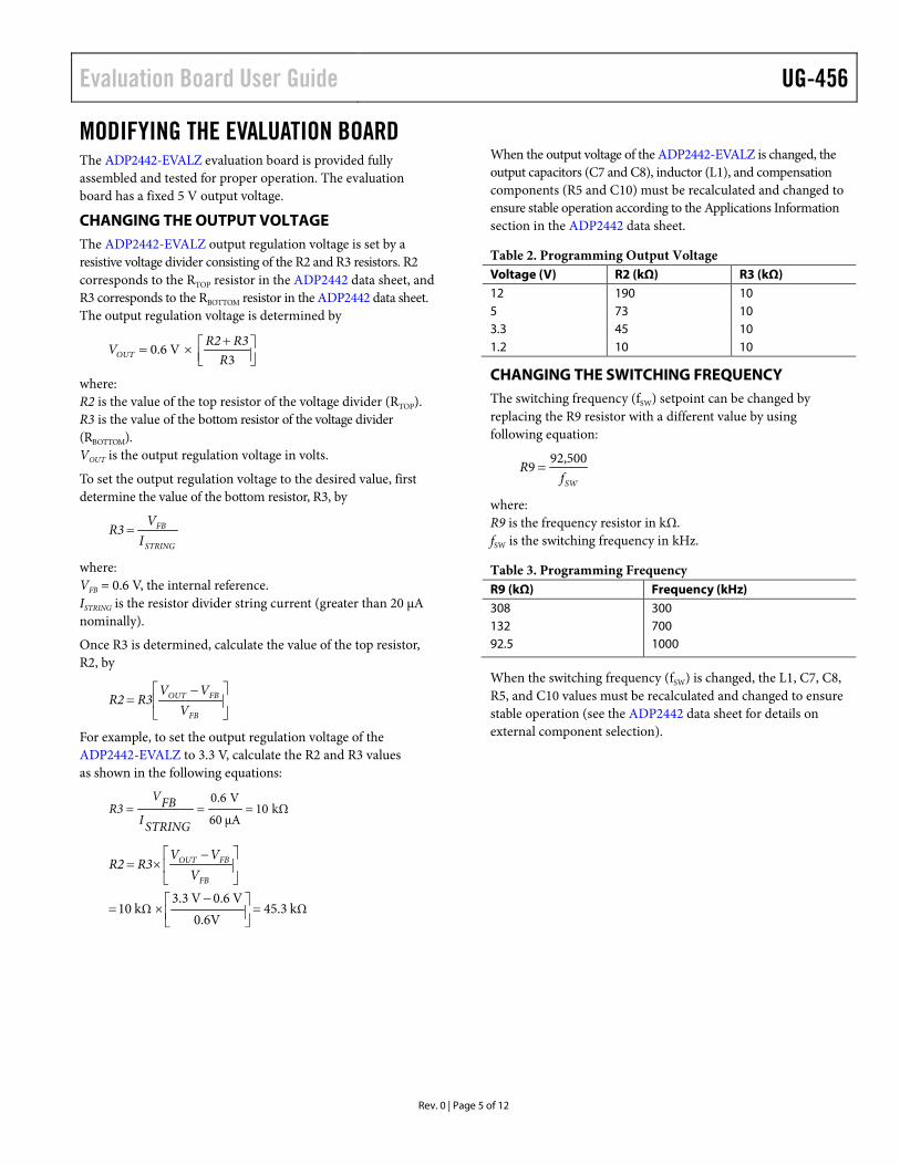
MODIFYING THE EVALUATION BOARD The ADP2442-EVALZ evaluation board is provided fully assembled and tested for proper operation. The evaluation board has a fixed 5 V output voltage.
CHANGING THE OUTPUT VOLTAGE The ADP2442-EVALZ output regulation voltage is set by a resistive voltage divider consisting of the R2 and R3 resistors. R2 corresponds to the RTOP resistor in the ADP2442 data sheet, and R3 corresponds to the RBOTTOM resistor in the ADP2442 data sheet. The output regulation voltage is determined by
+
×=3
V6.0RR3R2VOUT
where: R2 is the value of the top resistor of the voltage divider (RTOP). R3 is the value of the bottom resistor of the voltage divider (RBOTTOM). VOUT is the output regulation voltage in volts.
To set the output regulation voltage to the desired value, first determine the value of the bottom resistor, R3, by
STRING
FB
IV
R3 =
where: VFB = 0.6 V, the internal reference. ISTRING is the resistor divider string current (greater than 20 µA nominally).
Once R3 is determined, calculate the value of the top resistor, R2, by
−=
FB
FBOUT
VVV
R3R2
For example, to set the output regulation voltage of the ADP2442-EVALZ to 3.3 V, calculate the R2 and R3 values as shown in the following equations:
kΩ10μA60
V0.6===
STRINGIFBV
R3
ΩΩ k45.30.6V
V0.6V3.3k10 =
−
×=
−×=
FB
FBOUT
VVV
R3R2
When the output voltage of the ADP2442-EVALZ is changed, the output capacitors (C7 and C8), inductor (L1), and compensation components (R5 and C10) must be recalculated and changed to ensure stable operation according to the Applications Information section in the ADP2442 data sheet.
Table 2. Programming Output Voltage Voltage (V) R2 (kΩ) R3 (kΩ) 12 190 10 5 73 10 3.3 45 10 1.2 10 10
CHANGING THE SWITCHING FREQUENCY The switching frequency (fSW) setpoint can be changed by replacing the R9 resistor with a different value by using following equation:
SWfR 500,929 =
where: R9 is the frequency resistor in kΩ. fSW is the switching frequency in kHz.
Table 3. Programming Frequency R9 (kΩ) Frequency (kHz) 308 300 132 700 92.5 1000
When the switching frequency (fSW) is changed, the L1, C7, C8, R5, and C10 values must be recalculated and changed to ensure stable operation (see the ADP2442 data sheet for details on external component selection).
UG-456 Evaluation Board User Guide
Rev. 0 | Page 6 of 12
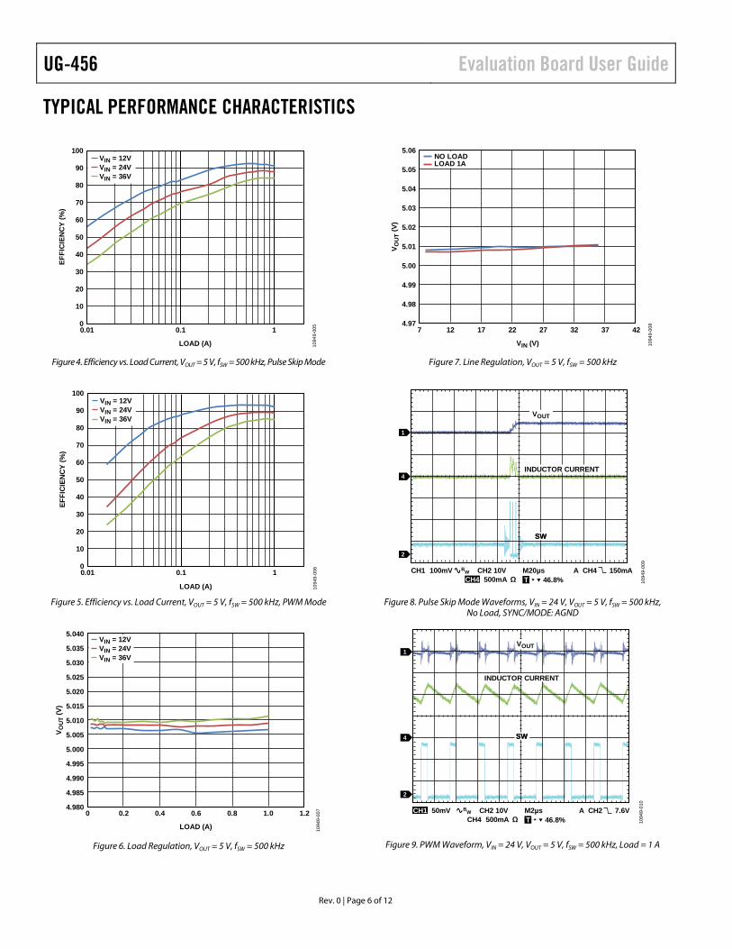
TYPICAL PERFORMANCE CHARACTERISTICS
Figure 4. Efficiency vs. Load Current, VOUT = 5 V, fSW = 500 kHz, Pulse Skip Mode
Figure 5. Efficiency vs. Load Current, VOUT = 5 V, fSW = 500 kHz, PWM Mode
Figure 6. Load Regulation, VOUT = 5 V, fSW = 500 kHz
Figure 7. Line Regulation, VOUT = 5 V, fSW = 500 kHz
Figure 8. Pulse Skip Mode Waveforms, VIN = 24 V, VOUT = 5 V, fSW = 500 kHz, No Load, SYNC/MODE: AGND
Figure 9. PWM Waveform, VIN = 24 V, VOUT = 5 V, fSW = 500 kHz, Load = 1 A
0
10
20
30
40
50
60
70
80
90
100
0.01 0.1 1
EFFI
CIE
NC
Y (%
)
LOAD (A)
VIN = 12VVIN = 24VVIN = 36V
1094
9-00
5
0
10
20
30
40
50
60
70
80
90
100
0.01 0.1 1
EFFI
CIE
NC
Y (%
)
VIN = 12VVIN = 24VVIN = 36V
1094
9-00
6
LOAD (A)
LOAD (A) 1094
9-00
74.980
4.985
4.990
4.995
5.000
5.005
5.010
5.015
5.020
5.025
5.030
5.035
5.040
0 0.2 0.4 0.6 0.8 1.0 1.2
V OU
T (V
)
VIN = 12VVIN = 24VVIN = 36V
1094
9-00
84.97
4.98
4.99
5.00
5.01
5.02
5.03
5.04
5.05
5.06
7 12 17 22 27 32 37 42
V OU
T (V
)
VIN (V)
NO LOADLOAD 1A
CH1 100mV CH2 10V M20µs A CH4 150mA
1
4
2
T 46.8%BWCH4 500mA Ω
VOUT
SWSW
INDUCTOR CURRENT
1094
9-00
9
CH1 50mV CH2 10V M2µs A CH2 7.6V
1
4
2
T 46.8%BWCH4 500mA Ω
VOUT
INDUCTOR CURRENT
SWSW
1094
9-01
0
Evaluation Board User Guide UG-456
Rev. 0 | Page 7 of 12
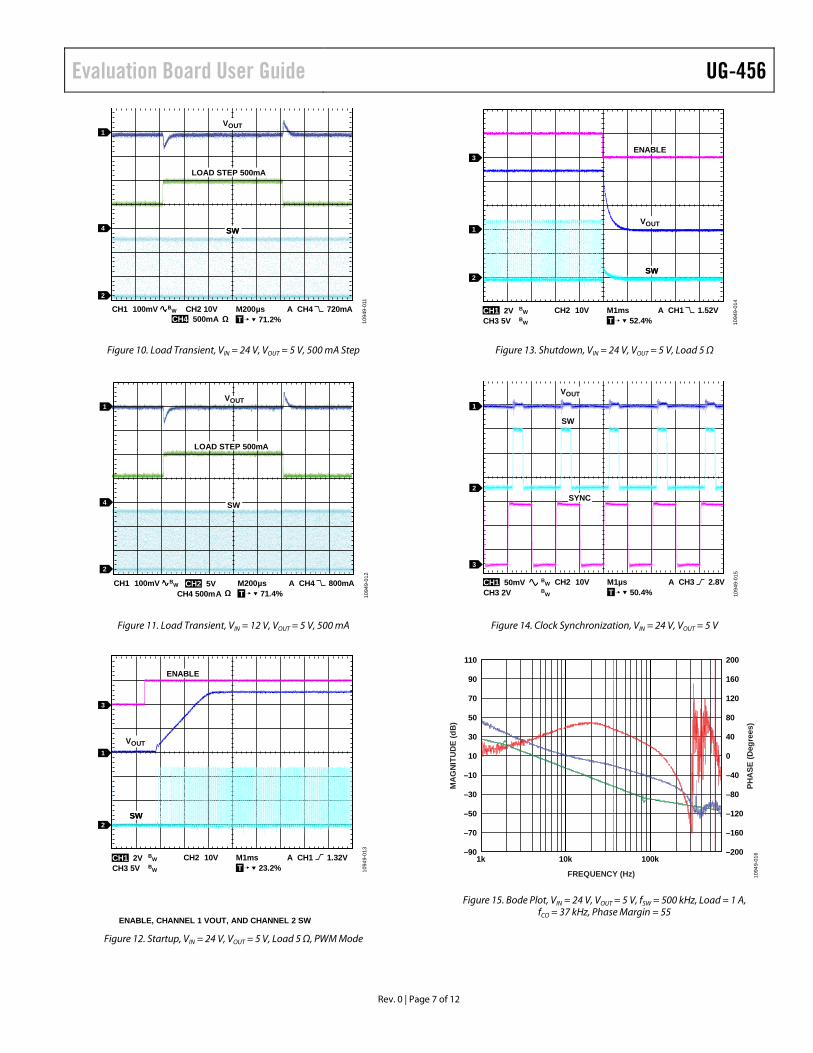
Figure 10. Load Transient, VIN = 24 V, VOUT = 5 V, 500 mA Step
Figure 11. Load Transient, VIN = 12 V, VOUT = 5 V, 500 mA
Figure 12. Startup, VIN = 24 V, VOUT = 5 V, Load 5 Ω, PWM Mode
Figure 13. Shutdown, VIN = 24 V, VOUT = 5 V, Load 5 Ω
Figure 14. Clock Synchronization, VIN = 24 V, VOUT = 5 V
Figure 15. Bode Plot, VIN = 24 V, VOUT = 5 V, fSW = 500 kHz, Load = 1 A, fCO = 37 kHz, Phase Margin = 55
CH1 100mV CH2 10V M200µs A CH4 720mA
1
4
2
T 71.2%BWCH4 500mA Ω
LOAD STEP 500mA
SWSW
1094
9-01
1
VOUT
CH1 100mVCH4 500mA
M200µs A CH4 800mA
1
4
2
T 71.4%BW CH2 5V
Ω
VOUT
LOAD STEP 500mA
SW
1094
9-01
2
CH2 10VCH3 5V
M1ms A CH1 1.32V
1
3
2
T 23.2%BWBW
CH1 2V
1094
9-01
3
ENABLE, CHANNEL 1 VOUT, AND CHANNEL 2 SW
SWSW
ENABLE
VOUT
CH2 10VCH3 5V
M1ms A CH1 1.52V
1
3
2
T 52.4%BWBW
CH1 2V
1094
9-01
4
SWSW
ENABLE
VOUT
CH2 10VCH3 2V
M1µs A CH3 2.8V
1
3
2
T 50.4%BWBW
CH1 50mV
1094
9-01
5
SW
SYNC
VOUT
200
–200
160
–160
120
–120
80
–80
40
–40
0
110
1k 10k 100k–90
90
–70
70
–50
50
–30
30
–10
10PH
ASE
(Deg
rees
)
MA
GN
ITU
DE
(dB
)
FREQUENCY (Hz) 1094
9-01
6
UG-456 Evaluation Board User Guide
Rev. 0 | Page 8 of 12
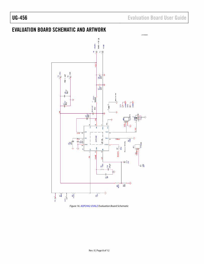
EVALUATION BOARD SCHEMATIC AND ARTWORK
Figure 16. ADP2442-EVALZ Evaluation Board Schematic
10949-017

Evaluation Board User Guide UG-456
Rev. 0 | Page 9 of 12
Figure 17. ADP2442-EVALZ Evaluation Board Top Layer
Figure 18. ADP2442-EVALZ Evaluation Board Third Layer
Figure 19. ADP2442-EVALZ Evaluation Board Second Layer
Figure 20. ADP2442-EVALZ Evaluation Board Bottom Layer
1094
9-01
810
949-
019
1094
9-02
010
949-
021
UG-456 Evaluation Board User Guide
Rev. 0 | Page 10 of 12
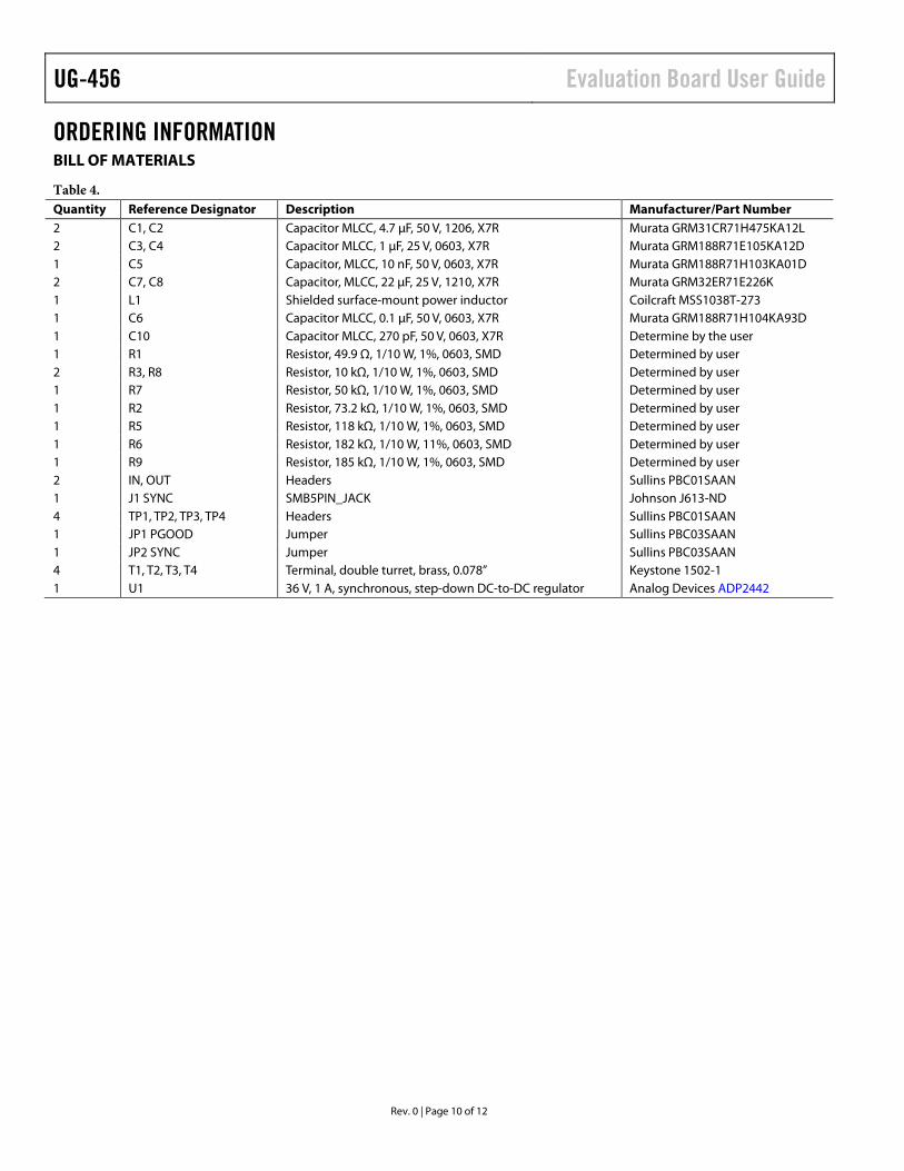
ORDERING INFORMATION BILL OF MATERIALS
Table 4. Quantity Reference Designator Description Manufacturer/Part Number 2 C1, C2 Capacitor MLCC, 4.7 µF, 50 V, 1206, X7R Murata GRM31CR71H475KA12L 2 C3, C4 Capacitor MLCC, 1 µF, 25 V, 0603, X7R Murata GRM188R71E105KA12D 1 C5 Capacitor, MLCC, 10 nF, 50 V, 0603, X7R Murata GRM188R71H103KA01D 2 C7, C8 Capacitor, MLCC, 22 µF, 25 V, 1210, X7R Murata GRM32ER71E226K 1 L1 Shielded surface-mount power inductor Coilcraft MSS1038T-273 1 C6 Capacitor MLCC, 0.1 µF, 50 V, 0603, X7R Murata GRM188R71H104KA93D 1 C10 Capacitor MLCC, 270 pF, 50 V, 0603, X7R Determine by the user 1 R1 Resistor, 49.9 Ω, 1/10 W, 1%, 0603, SMD Determined by user 2 R3, R8 Resistor, 10 kΩ, 1/10 W, 1%, 0603, SMD Determined by user 1 R7 Resistor, 50 kΩ, 1/10 W, 1%, 0603, SMD Determined by user 1 R2 Resistor, 73.2 kΩ, 1/10 W, 1%, 0603, SMD Determined by user 1 R5 Resistor, 118 kΩ, 1/10 W, 1%, 0603, SMD Determined by user 1 R6 Resistor, 182 kΩ, 1/10 W, 11%, 0603, SMD Determined by user 1 R9 Resistor, 185 kΩ, 1/10 W, 1%, 0603, SMD Determined by user 2 IN, OUT Headers Sullins PBC01SAAN 1 J1 SYNC SMB5PIN_JACK Johnson J613-ND 4 TP1, TP2, TP3, TP4 Headers Sullins PBC01SAAN 1 JP1 PGOOD Jumper Sullins PBC03SAAN 1 JP2 SYNC Jumper Sullins PBC03SAAN 4 T1, T2, T3, T4 Terminal, double turret, brass, 0.078” Keystone 1502-1 1 U1 36 V, 1 A, synchronous, step-down DC-to-DC regulator Analog Devices ADP2442

Evaluation Board User Guide UG-456
Rev. 0 | Page 11 of 12
NOTES
UG-456 Evaluation Board User Guide
Rev. 0 | Page 12 of 12
NOTES
ESD Caution ESD (electrostatic discharge) sensitive device. Charged devices and circuit boards can discharge without detection. Although this product features patented or proprietary protection circuitry, damage may occur on devices subjected to high energy ESD. Therefore, proper ESD precautions should be taken to avoid performance degradation or loss of functionality.
Legal Terms and Conditions By using the evaluation board discussed herein (together with any tools, components documentation or support materials, the “Evaluation Board”), you are agreeing to be bound by the terms and conditions set forth below (“Agreement”) unless you have purchased the Evaluation Board, in which case the Analog Devices Standard Terms and Conditions of Sale shall govern. Do not use the Evaluation Board until you have read and agreed to the Agreement. Your use of the Evaluation Board shall signify your acceptance of the Agreement. This Agreement is made by and between you (“Customer”) and Analog Devices, Inc. (“ADI”), with its principal place of business at One Technology Way, Norwood, MA 02062, USA. Subject to the terms and conditions of the Agreement, ADI hereby grants to Customer a free, limited, personal, temporary, non-exclusive, non-sublicensable, non-transferable license to use the Evaluation Board FOR EVALUATION PURPOSES ONLY. Customer understands and agrees that the Evaluation Board is provided for the sole and exclusive purpose referenced above, and agrees not to use the Evaluation Board for any other purpose. Furthermore, the license granted is expressly made subject to the following additional limitations: Customer shall not (i) rent, lease, display, sell, transfer, assign, sublicense, or distribute the Evaluation Board; and (ii) permit any Third Party to access the Evaluation Board. As used herein, the term “Third Party” includes any entity other than ADI, Customer, their employees, affiliates and in-house consultants. The Evaluation Board is NOT sold to Customer; all rights not expressly granted herein, including ownership of the Evaluation Board, are reserved by ADI. CONFIDENTIALITY. This Agreement and the Evaluation Board shall all be considered the confidential and proprietary information of ADI. Customer may not disclose or transfer any portion of the Evaluation Board to any other party for any reason. Upon discontinuation of use of the Evaluation Board or termination of this Agreement, Customer agrees to promptly return the Evaluation Board to ADI. ADDITIONAL RESTRICTIONS. Customer may not disassemble, decompile or reverse engineer chips on the Evaluation Board. Customer shall inform ADI of any occurred damages or any modifications or alterations it makes to the Evaluation Board, including but not limited to soldering or any other activity that affects the material content of the Evaluation Board. Modifications to the Evaluation Board must comply with applicable law, including but not limited to the RoHS Directive. TERMINATION. ADI may terminate this Agreement at any time upon giving written notice to Customer. Customer agrees to return to ADI the Evaluation Board at that time. LIMITATION OF LIABILITY. THE EVALUATION BOARD PROVIDED HEREUNDER IS PROVIDED “AS IS” AND ADI MAKES NO WARRANTIES OR REPRESENTATIONS OF ANY KIND WITH RESPECT TO IT. ADI SPECIFICALLY DISCLAIMS ANY REPRESENTATIONS, ENDORSEMENTS, GUARANTEES, OR WARRANTIES, EXPRESS OR IMPLIED, RELATED TO THE EVALUATION BOARD INCLUDING, BUT NOT LIMITED TO, THE IMPLIED WARRANTY OF MERCHANTABILITY, TITLE, FITNESS FOR A PARTICULAR PURPOSE OR NONINFRINGEMENT OF INTELLECTUAL PROPERTY RIGHTS. IN NO EVENT WILL ADI AND ITS LICENSORS BE LIABLE FOR ANY INCIDENTAL, SPECIAL, INDIRECT, OR CONSEQUENTIAL DAMAGES RESULTING FROM CUSTOMER’S POSSESSION OR USE OF THE EVALUATION BOARD, INCLUDING BUT NOT LIMITED TO LOST PROFITS, DELAY COSTS, LABOR COSTS OR LOSS OF GOODWILL. ADI’S TOTAL LIABILITY FROM ANY AND ALL CAUSES SHALL BE LIMITED TO THE AMOUNT OF ONE HUNDRED US DOLLARS ($100.00). EXPORT. Customer agrees that it will not directly or indirectly export the Evaluation Board to another country, and that it will comply with all applicable United States federal laws and regulations relating to exports. GOVERNING LAW. This Agreement shall be governed by and construed in accordance with the substantive laws of the Commonwealth of Massachusetts (excluding conflict of law rules). Any legal action regarding this Agreement will be heard in the state or federal courts having jurisdiction in Suffolk County, Massachusetts, and Customer hereby submits to the personal jurisdiction and venue of such courts. The United Nations Convention on Contracts for the International Sale of Goods shall not apply to this Agreement and is expressly disclaimed.
©2012 Analog Devices, Inc. All rights reserved. Trademarks and registered trademarks are the property of their respective owners. UG10949-0-11/12(0)