Embed Size (px)
Citation preview
_______________________________________________________________ Maxim Integrated Products 1
For pricing, delivery, and ordering information, please contact Maxim Direct at 1-888-629-4642, or visit Maxim’s website at www.maxim-ic.com.
10-Channel Scan Driver for TFT LCD with GPM Function M
AX
17
11
919-4952; Rev 0; 12/09
General DescriptionThe MAX17119 includes a 10-channel, high-voltage, level-shifting scan driver with a gate-pulse modulation (GPM) feature to shape the corner of the scan-driver out-put to reduce flicker. The device is optimized for thin-film transistor (TFT) liquid-crystal display (LCD) applications.
The high-voltage level-shifting scan driver is designed to drive the TFT panel gate logic. Its 10 outputs swing from +38V (maximum) to -12V (minimum) and can swiftly drive capacitive loads. There are two positive supply inputs that provide flexibility for system design.
The GPM feature is employed to shape the corner of the falling edge of the clock channels. This reduces flicker, and therefore improves the display quality.
The MAX17119 also features a dedicated discharge channel and an integrated voltage detector. When the system shuts down, the voltage detector commands the discharge channel to swing its output to positive sup-ply voltage so as to remove any residual image on the display quickly.
The MAX17119 is available in a 28-pin, 5mm x 5mm, thin QFN package with a maximum thickness of 0.8mm for thin LCD panels.
ApplicationsLCD Monitors
LCD TVs
FeaturesS High-Voltage Level-Shifting Scan Drivers
Logic-Level Inputs +38V to -12V Outputs GPM Feature Discharge Channel
S Thermal-Overload Protection
S 28-Pin, 5mm x 5mm Thin QFN Package
Ordering Information
+Denotes lead(Pb)-free/RoHS-compliant package.
EVALUATION KIT
AVAILABLE
PART TEMP RANGE PIN-PACKAGE
MAX17119ETI+ -40NC to +85NC 28 TQFN

10-Channel Scan Driver for TFT LCD with GPM Function
MA
X1
71
19
2 ______________________________________________________________________________________
Stresses beyond those listed under “Absolute Maximum Ratings” may cause permanent damage to the device. These are stress ratings only, and functional operation of the device at these or any other conditions beyond those indicated in the operational sections of the specifications is not implied. Exposure to absolute maximum rating conditions for extended periods may affect device reliability.
A1–A9, VSENSE, FLK1, FLK2, FLK3 to GND ..........-0.3V to +6VGON1, GON2 to GND ...........................................-0.3V to +40VGOFF to GND ........................................................-14V to +0.3VY1–Y7, YDCHG to GND ........(VGOFF - 0.3V) to (VGON1 + 0.3V)Y8, Y9 to GND ....................... (VGOFF - 0.3V) to (VGON2 + 0.3V)RE to GND ............................................ -0.3V to (VGON1 + 0.3V)Y1–Y6 to RE ...........................(VGOFF - 0.3V) to (VGON1 + 0.3V)Y1–Y6, YDCHG Load RMS Current .................................350mAGON1 RMS Current ........................................................600mA
GON2 RMS Current ..........................................................380mAGOFF RMS Current ..........................................................600mAContinuous Power Dissipation (TA = +70NC) 28-Pin, 5mm x 5mm TQFN (derate 34.5mW/NC above +70NC)..........................2758.6mWOperating Temperature Range .......................... -40NC to +85NCJunction Temperature .....................................................+150NCStorage Temperature Range ............................ -65NC to +150NCLead Temperature (soldering, 10s) ................................+300NC
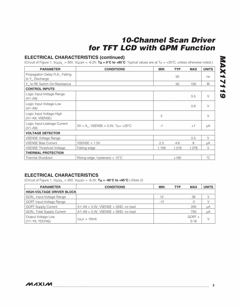
ELECTRICAL CHARACTERISTICS(Circuit of Figure 1, VGON_ = 30V, VGOFF = -6.2V, TA = 0°C to +85°C. Typical values are at TA = +25°C, unless otherwise noted.)
ABSOLUTE MAXIMUM RATINGS
PARAMETER CONDITIONS MIN TYP MAX UNITS
HIGH-VOLTAGE DRIVER BLOCK
GON_ Input-Voltage Range 12 38 V
GOFF Input-Voltage Range -12 -2 V
GOFF Supply Current A1–A9 = 3.3V, VSENSE = GND, no load 100 200 FA
GON_ Total Supply Current A1–A9 = 3.3V, VSENSE = GND, no load 450 750 FA
Output Voltage Low (Y1–Y9, YDCHG)
IOUT = 10mA GOFF +
0.08GOFF +
0.16V
Output Voltage High (Y1–Y7, YDCHG)
IOUT = 10mA GON1 -
0.16GON1 -
0.08V
Output Voltage High (Y8, Y9) IOUT = 10mA GON2 -
0.16GON2 -
0.08V
Rise Time (Y1–Y7, YDCHG)TA = +25NC , VGON1 = 30V and VGOFF = -6.2V (Note 1)
50 200 ns
Fall Time (Y1–Y7, YDCHG)TA = +25NC , VGON1 = 30 V and VGOFF = -6.2V (Note 1)
40 120 ns
Rise Time (Y8, Y9)TA = +25NC , VGON2 = 30V and VGOFF = -6.2V (Note 1)
50 200 ns
Fall Time (Y8, Y9)TA = +25NC , VGON2 = 30V and VGOFF = -6.2V (Note 1)
40 120 ns
Propagation Delay A_ Rising to Y_ Rising, VSENSE Falling to YDCHG Rising
With VGON_= 30V and VGOFF = -6.2V (Note 1) 50 ns
Propagation Delay A_ Falling to Y_ Falling, VSENSE Rising to YDCHG Falling
With VGON_= 30V and VGOFF = -6.2V (Note 1) 50 ns
10-Channel Scan Driver for TFT LCD with GPM Function
MA
X1
71
19
_______________________________________________________________________________________ 3
ELECTRICAL CHARACTERISTICS(Circuit of Figure 1, VGON_ = 30V, VGOFF = -6.2V, TA = -40°C to +85°C.) (Note 2)
ELECTRICAL CHARACTERISTICS (continued)(Circuit of Figure 1, VGON_ = 30V, VGOFF = -6.2V, TA = 0°C to +85°C. Typical values are at TA = +25°C, unless otherwise noted.)
PARAMETER CONDITIONS MIN TYP MAX UNITS
Propagation Delay FLK_ Falling to Y_ Discharge
50 ns
Y_ to RE Switch On-Resistance 50 100 I
CONTROL INPUTS
Logic Input-Voltage Range (A1–A9)
5.5 V
Logic Input Voltage Low (A1–A9)
0.8 V
Logic Input Voltage High (A1–A9, VSENSE)
2 V
Logic Input-Leakage Current (A1–A9)
0V < A_, VSENSE < 5.5V, TA= +25°C -1 +1 FA
VOLTAGE DETECTOR
VSENSE Voltage Range 5.5 V
VSENSE Bias Current VSENSE = 1.5V 2.3 4.6 8 FA
VSENSE Threshold Voltage Falling edge 1.158 1.218 1.278 V
THERMAL PROTECTION
Thermal Shutdown Rising edge, hysteresis = 15NC +160 NC
PARAMETER CONDITIONS MIN TYP MAX UNITS
HIGH-VOLTAGE DRIVER BLOCK
GON_ Input-Voltage Range 12 38 V
GOFF Input-Voltage Range -12 -2 V
GOFF Supply Current A1–A9 = 3.3V, VSENSE = GND, no load 200 FA
GON_ Total Supply Current A1–A9 = 3.3V, VSENSE = GND, no load 750 FA
Output Voltage Low (Y1–Y9, YDCHG)
IOUT = 10mA GOFF +
0.16V

10-Channel Scan Driver for TFT LCD with GPM Function
MA
X1
71
19
4 ______________________________________________________________________________________
ELECTRICAL CHARACTERISTICS (continued)(Circuit of Figure 1, VGON_ = 30V, VGOFF = -6.2V, TA = -40°C to +85°C.) (Note 2)
Note 1: The panel models for different channels are illustrated in Figure 4.Note 2: -40°C specs are guaranteed by design, not production tested.
PARAMETER CONDITIONS MIN TYP MAX UNITS
Output Voltage High (Y1–Y7, YDCHG)
IOUT = 10mA GON1 -
0.16V
Output Voltage High (Y8, Y9) IOUT = 10mA GON2 -
0.16V
Rise Time (Y1–Y7, YDCHG)TA = +25NC, VGON1 = 30V and VGOFF = -6.2V (Note 1)
200 ns
Fall Time (Y1–Y7, YDCHG)TA = +25NC, VGON1 = 30V and VGOFF = -6.2V (Note 1)
120 ns
Rise Time (Y8, Y9)TA = +25oC, VGON2 = 30V and VGOFF = -6.2V (Note 1)
200 ns
Fall Time (Y8, Y9)TA = +25NC , VGON2 = 30V and VGOFF = -6.2V (Note 1)
120 ns
Y_ to RE Switch On-Resistance 100 I
CONTROL INPUTS
Logic Input-Voltage Range (A1–A9)
5.5 V
Logic Input Voltage Low (A1–A9)
0.8 V
Logic Input Voltage High (A1–A9)
2 V
VOLTAGE DETECTOR
VSENSE Voltage Range 5.5 V
VSENSE Threshold Voltage Falling edge 1.158 1.278 V
VSENSE Pullup Current VSENSE = 1.5V 2.3 8 FA
10-Channel Scan Driver for TFT LCD with GPM Function
MA
X1
71
19
_______________________________________________________________________________________ 5
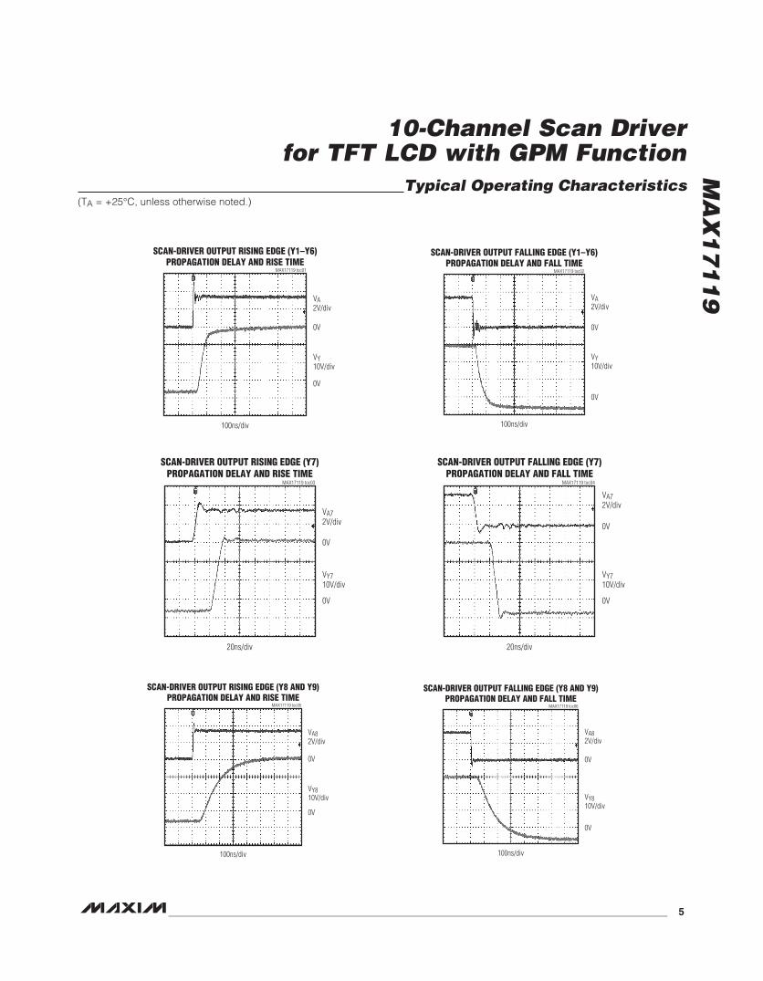
Typical Operating Characteristics(TA = +25°C, unless otherwise noted.)
SCAN-DRIVER OUTPUT FALLING EDGE (Y8 AND Y9)PROPAGATION DELAY AND FALL TIME
MAX17119 toc06
0V
0V
VY810V/div
VA82V/div
100ns/div
SCAN-DRIVER OUTPUT RISING EDGE (Y8 AND Y9)PROPAGATION DELAY AND RISE TIME
MAX17119 toc05
0V
0V
VY810V/div
VA82V/div
100ns/div
SCAN-DRIVER OUTPUT FALLING EDGE (Y7)PROPAGATION DELAY AND FALL TIME
MAX17119 toc04
0V
0V
VY710V/div
VA72V/div
20ns/div
SCAN-DRIVER OUTPUT RISING EDGE (Y7)PROPAGATION DELAY AND RISE TIME
MAX17119 toc03
0V
0V
VY710V/div
VA72V/div
20ns/div
SCAN-DRIVER OUTPUT FALLING EDGE (Y1–Y6)PROPAGATION DELAY AND FALL TIME
MAX17119 toc02
0V
0V
VY10V/div
VA2V/div
100ns/div
SCAN-DRIVER OUTPUT RISING EDGE (Y1–Y6)PROPAGATION DELAY AND RISE TIME
MAX17119 toc01
0V
0V
VY10V/div
VA2V/div
100ns/div
10-Channel Scan Driver for TFT LCD with GPM Function
MA
X1
71
19
6 ______________________________________________________________________________________
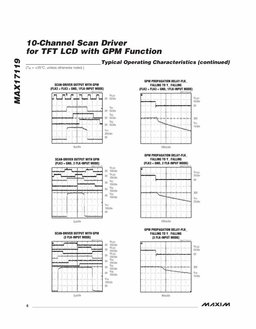
Typical Operating Characteristics (continued)(TA = +25°C, unless otherwise noted.)
GPM PROPAGATION DELAY-FLK_FALLING TO Y_ FALLING
(3 FLK-INPUT MODE)MAX17119 toc12
0V
30V
VY41V/div
VFLK25V/div
40ns/div
SCAN-DRIVER OUTPUT WITH GPM (3 FLK-INPUT MODE)
MAX17119 toc11
0V
0V
0V
0V
0V
VY410V/div
VA510V/div
0VVA610V/div
VA410V/div
VFLK210V/div
0VVFLK310V/div
VFLK110V/div
2Fs/div
GPM PROPAGATION DELAY-FLK_FALLING TO Y_ FALLING
(FLK3 = GND, 2 FLK-INPUT MODE)MAX17119 toc10
0V
30V
VY12V/div
VFLK25V/div
100ns/div
SCAN-DRIVER OUTPUT WITH GPM(FLK3 = GND, 2 FLK-INPUT MODE)
MAX17119 toc09
0V
0V
0V
0V
0V
VY110V/div
VA210V/div
0VVA310V/div
VA110V/div
VFLK210V/div
VFLK110V/div
2Fs/div
GPM PROPAGATION DELAY-FLK_FALLING TO Y_ FALLING
(FLK2 = FLK3 = GND, 1FLK-INPUT MODE)MAX17119 toc08
0V
30V
VY11V/div
VFLK15V/div
100ns/div
SCAN-DRIVER OUTPUT WITH GPM (FLK2 = FLK3 = GND, 1FLK-INPUT MODE)
MAX17119 toc07
0V
0V
0V
0V
0V
VY120V/div
VA35V/div
VA25V/div
VA15V/div
VFLK15V/div
4Fs/div

10-Channel Scan Driver for TFT LCD with GPM Function
MA
X1
71
19
_______________________________________________________________________________________ 7
Pin Configuration
Pin Description
MAX17119
TQFN5mm x 5mm
TOP VIEW
26
27
25
24
10
9
11
A8 A6 A5 A4 A3
12
A9
Y8 Y6 Y5Y9 Y4 Y3
1 2
FLK3
4 5 6 7
2021 19 17 16 15
FLK2
FLK1
GON2
GOFF
GON1
A1
A7
Y7
3
18
28 8VSENSE A2
RE
23 13 Y1GND
22 14 Y2YDCHG
+
PIN NAME FUNCTION
1–9 A9–A1 Level-Shifter Logic-Level Input
10 GON1Gate-On Supply Input 1. GON1 is the positive supply for the Y1–Y7 and YDCHG level shifters. Bypass GON1 to ground with a minimum of 1FF ceramic capacitor.
11 GOFFGate-Off Supply Input. GOFF is the negative supply for the Y1–Y9 and YDCHG. Bypass GOFF to ground with a minimum of 1FF ceramic capacitor.
12 GON2Gate-On Supply Input 2. GON2 is the positive supply for the Y8 and Y9 level shifters. Bypass GON2 to ground with a minimum of 1FF ceramic capacitor.
13–21 Y1–Y9 Level-Shifter Outputs
22 YDCHG Level-Shifter Output for Discharge Function
23 GND Ground
24 RE Resistor Connection Input for GPM Function
25 FLK3 GPM Control Input for Level-Shifter Outputs Y3 and Y6
26 FLK2 GPM Control Input for Level-Shifter Outputs Y2 and Y5
27 FLK1 GPM Control Input for Level-Shifter Outputs Y1 and Y4
28 VSENSE
Input Voltage Sense for Voltage Detector. This pin is usually connected to VLOGIC in the system through a resistor-divider (R1 and R2). When VVSENSE is below its threshold, the discharge channel of the level-shifter channel is turned on and YDCHG is connected to GON1 internally. There is a 4.6FA internal pullup current on VSENSE and both R1 and R2 should be less than 50kI.
— EPExposed Backside Pad. Connect to GOFF. Copper area should be maximized for thermal performance.
10-Channel Scan Driver for TFT LCD with GPM Function
MA
X1
71
19
8 ______________________________________________________________________________________
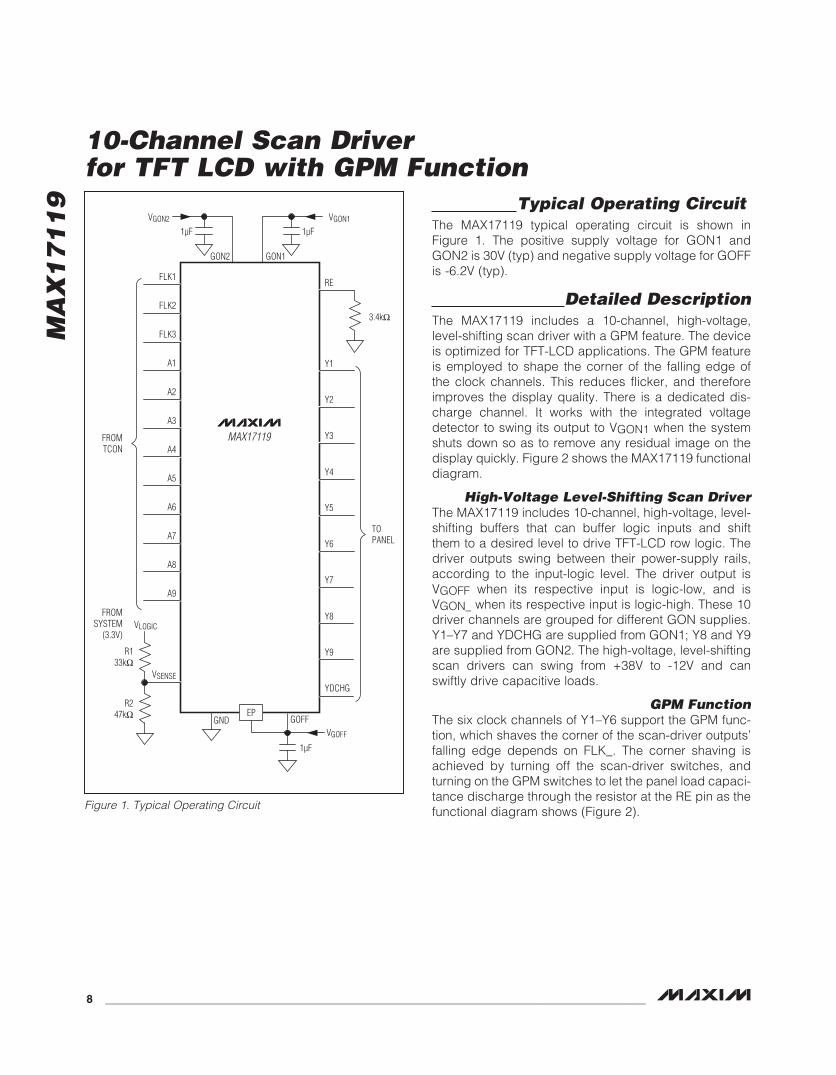
Typical Operating CircuitThe MAX17119 typical operating circuit is shown in Figure 1. The positive supply voltage for GON1 and GON2 is 30V (typ) and negative supply voltage for GOFF is -6.2V (typ).
Detailed DescriptionThe MAX17119 includes a 10-channel, high-voltage, level-shifting scan driver with a GPM feature. The device is optimized for TFT-LCD applications. The GPM feature is employed to shape the corner of the falling edge of the clock channels. This reduces flicker, and therefore improves the display quality. There is a dedicated dis-charge channel. It works with the integrated voltage detector to swing its output to VGON1 when the system shuts down so as to remove any residual image on the display quickly. Figure 2 shows the MAX17119 functional diagram.
High-Voltage Level-Shifting Scan DriverThe MAX17119 includes 10-channel, high-voltage, level-shifting buffers that can buffer logic inputs and shift them to a desired level to drive TFT-LCD row logic. The driver outputs swing between their power-supply rails, according to the input-logic level. The driver output is VGOFF when its respective input is logic-low, and is VGON_ when its respective input is logic-high. These 10 driver channels are grouped for different GON supplies. Y1–Y7 and YDCHG are supplied from GON1; Y8 and Y9 are supplied from GON2. The high-voltage, level-shifting scan drivers can swing from +38V to -12V and can swiftly drive capacitive loads.
GPM FunctionThe six clock channels of Y1–Y6 support the GPM func-tion, which shaves the corner of the scan-driver outputs’ falling edge depends on FLK_. The corner shaving is achieved by turning off the scan-driver switches, and turning on the GPM switches to let the panel load capaci-tance discharge through the resistor at the RE pin as the functional diagram shows (Figure 2).Figure 1. Typical Operating Circuit
GON2 GON1
FLK1
FLK2
FLK3
A1
A2
A3
A4
A5
A6
A7
A8
A9
VSENSE
VGON1VGON2
VLOGIC
R247kI
R133kI
3.4kI
FROMSYSTEM
(3.3V)
FROMTCON
TOPANEL
YDCHG
GOFFGND
1µF
1µF1µF
VGOFF
EP
Y9
Y8
Y7
Y6
Y5
Y4
Y3
Y2
Y1
RE
MAX17119

10-Channel Scan Driver for TFT LCD with GPM Function
MA
X1
71
19
_______________________________________________________________________________________ 9
Figure 2. MAX17119 Functional Diagram
FLK1
FLK2
FLK3
A1
A2
A3
A4
A5
A6
A7
A8
A9
VSENSE
YDCHG
Y9
Y8
Y7
Y6
Y5
Y4
Y3
Y2
Y1
RE
GON1
LDO
GATEDRIVELOGICANDGPM
CONTROL
REF
REF
GND GON2 GOFF
VGOFF
EP
VLOGIC
VGON2
COMP
MAX17119VGON1
10-Channel Scan Driver for TFT LCD with GPM Function
MA
X1
71
19
10 _____________________________________________________________________________________
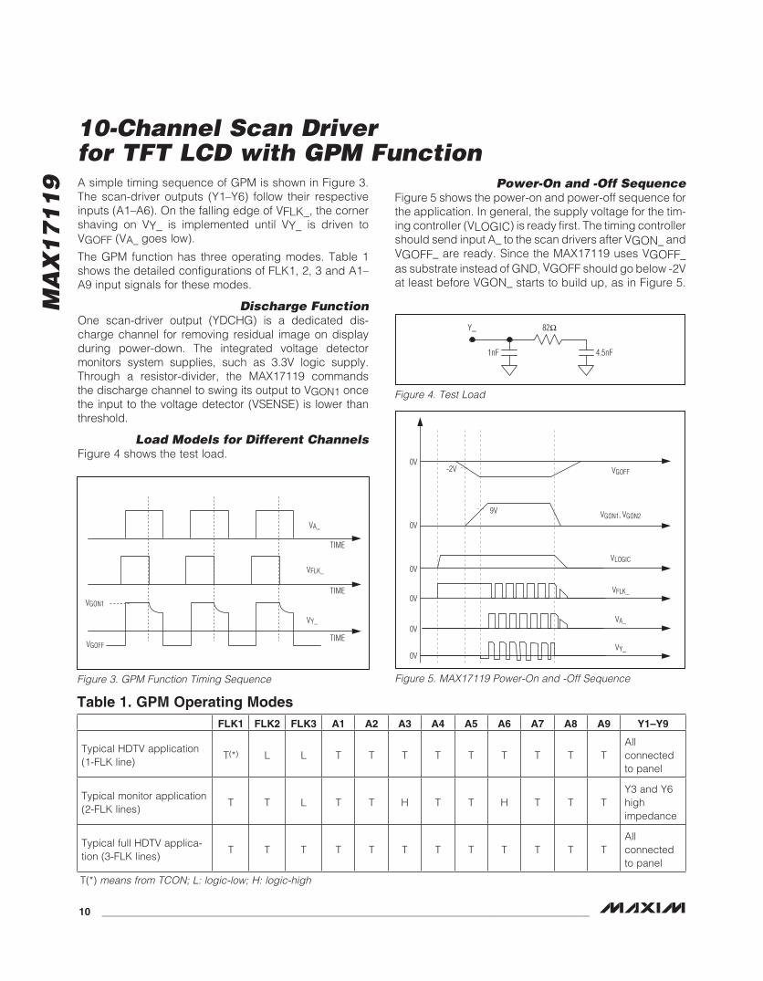
A simple timing sequence of GPM is shown in Figure 3. The scan-driver outputs (Y1–Y6) follow their respective inputs (A1–A6). On the falling edge of VFLK_, the corner shaving on VY_ is implemented until VY_ is driven to VGOFF (VA_ goes low).
The GPM function has three operating modes. Table 1 shows the detailed configurations of FLK1, 2, 3 and A1–A9 input signals for these modes.
Discharge FunctionOne scan-driver output (YDCHG) is a dedicated dis-charge channel for removing residual image on display during power-down. The integrated voltage detector monitors system supplies, such as 3.3V logic supply. Through a resistor-divider, the MAX17119 commands the discharge channel to swing its output to VGON1 once the input to the voltage detector (VSENSE) is lower than threshold.
Load Models for Different ChannelsFigure 4 shows the test load.
Power-On and -Off SequenceFigure 5 shows the power-on and power-off sequence for the application. In general, the supply voltage for the tim-ing controller (VLOGIC) is ready first. The timing controller should send input A_ to the scan drivers after VGON_ and VGOFF_ are ready. Since the MAX17119 uses VGOFF_ as substrate instead of GND, VGOFF should go below -2V at least before VGON_ starts to build up, as in Figure 5.
Figure 3. GPM Function Timing Sequence
Table 1. GPM Operating Modes
T(*) means from TCON; L: logic-low; H: logic-high
Figure 4. Test Load
Figure 5. MAX17119 Power-On and -Off Sequence
82IY_
1nF 4.5nF
0V-2V
9V
0V
0V
0V
0V
0V
VGOFF
VLOGIC
VFLK_
VA_
VY_
VGON1, VGON2
VGON1
VA_
VFLK_
TIME
TIME
TIME
VY_
VGOFF
FLK1 FLK2 FLK3 A1 A2 A3 A4 A5 A6 A7 A8 A9 Y1–Y9
Typical HDTV application(1-FLK line)
T(*) L L T T T T T T T T TAll connected to panel
Typical monitor application(2-FLK lines)
T T L T T H T T H T T TY3 and Y6high impedance
Typical full HDTV applica-tion (3-FLK lines)
T T T T T T T T T T T TAll connected to panel

10-Channel Scan Driver for TFT LCD with GPM Function
MA
X1
71
19
Maxim cannot assume responsibility for use of any circuitry other than circuitry entirely embodied in a Maxim product. No circuit patent licenses are implied. Maxim reserves the right to change the circuitry and specifications without notice at any time.
Maxim Integrated Products, 120 San Gabriel Drive, Sunnyvale, CA 94086 408-737-7600 11
© 2009 Maxim Integrated Products Maxim is a registered trademark of Maxim Integrated Products, Inc.
Thermal ProtectionThe MAX17119 includes a thermal-protection circuit. Thermal-overload protection prevents excessive power dissipation from overheating the MAX17119. When the junction temperature exceeds TJ = +160NC (typ), the device shuts down and all the outputs are put into high-impedance mode. The thermal protection is not latched and the device recovers once the temperature drops below the hysteretic threshold (+15NC typ).
Applications InformationPower Dissipation
An IC’s maximum power dissipation depends on the thermal resistance from the die to the ambient environ-ment and the ambient temperature. The thermal resis-tance depends on the IC package, PCB copper area, other thermal mass, and airflow. More PCB copper, cool-er ambient air, and more airflow increase the possible dissipation, while less copper or warmer air decreases the IC’s dissipation capability. The major component of power dissipation is the power dissipated in the high-voltage scan drivers.
When driving a pure capacitive load, the power dissipat-ed by the scan-driver outputs depends on the scan fre-quency, the capacitive load, and the difference between the GON_ and GOFF supply voltages. Assuming only
A7, A8, and A9 drive a very light load and that the power loss associated is negligible, the power loss is:
PDSCAN = 6 x CPANEL x (VGON1 - VGOFF)2 x fSCAN
If the six scan drivers (A1–A6) operate at a frequency of 50kHz, the load of the six outputs is 5nF, and the supply voltage difference is 30V, then the power dissipated is 1.35W.
PCB Layout and GroundingCareful PCB layout is important for proper operation. Use the following guidelines for good PCB layout:
• Avoid using vias in the high-current paths. If vias are unavoidable, use many vias in parallel to reduce resis-tance and inductance.
• Create a GOFF plane and connect it to EP.
• Create a ground island (GND) consisting of the supply capacitors’ grounds and GND pin.
• Connect all these together with short, wide traces or a small ground plane.
• Place the capacitors as close as possible to the respective supply voltage pins (GON1, GON2, and GOFF).
Refer to the MAX17119 Evaluation Kit for an example of proper board layout.
PACKAGE TYPE PACKAGE CODE DOCUMENT NO.
8 TQFN T2855+6 21-0139
Package InformationFor the latest package outline information and land pat-terns, go to www.maxim-ic.com/packages. Note that a “+”, “#”, or “-” in the package code indicates RoHS status only. Package drawings may show a different suf-fix character, but the drawing pertains to the package regardless of RoHS status.
Chip InformationPROCESS: BiCMOS


![SAMSUNG TFT-LCD MODEL A460HN08W(HD,60HZ) · LTY[Z]460HN05 is a color active matrix liquid crystal display (LCD) that uses amorphous silicon TFT(Thin Film Transistor) as switching](https://img.pdfslide.net/doc/110x75/5e813674375a7e757f1cdfd4/samsung-tft-lcd-model-a460hn08whd60hz-ltyz460hn05-is-a-color-active-matrix.jpg)