Embed Size (px)
Citation preview

General DescriptionThe MAX5944 is a dual, current limiter/low-drop ORing,switch controller power-management IC for FireWire®
applications. Each independent channel controls twoexternal power MOSFETs to regulate current from theinput power supply to the load and performs low-voltage-drop power-supply ORing. The MAX5944 operates overthe 7.5V to 37V input range and provides inrush and out-put current limit in addition to diode ORing functions suit-able for FireWire applications.
The MAX5944 allows the safe insertion and removal ofFireWire peripherals into a live FireWire port by providinginrush current control and output current-limiting func-tions. The MAX5944 features a current-limit function thatactively limits the current drawn by the load with a 2mstimeout. Its autoretry function then automatically restartsafter the 259ms autoretry delay time.
The ORing feature provides a very efficient way to pro-tect the FireWire port when connected to anotherFireWire peripheral that sources a higher voltage. Byturning off the external MOSFETS, the MAX5944 providesa true bidirectional load disconnect. Each channel hasan independent ON/OFF control that results in less than10µA supply current per channel.
The MAX5944 operates over the -40°C to +85°Cextended temperature range and is available in a 16-pin SO package.
ApplicationsFireWire Desktop/Notebook Port
FireWire Peripheral Device Current Limit
FireWire Hub
Hot Swap
Features♦ Provides Safe Hot-Swap for 7.5V to 37V Power
Supplies
♦ Dual-Channel Hot-Swap
♦ Low-Drop Power ORing with Ultra-Fast Turn-Off
♦ Active Current Limit
♦ ±5% Current-Limit Sensing Accuracy
♦ 2ms Current-Limit Timeout
♦ Fast Current-Limit Response to Output Short-Circuit Conditions
♦ Drives External n-Channel Power MOSFETs
♦ Independent Overcurrent Fault Status Outputs
♦ 259ms Autoretry Period
♦ 10µA (Per Channel) Shutdown Current
♦ Independent ON/OFF Control AllowsUndervoltage Lockout Programming
♦ Fast Load Disconnect Control Through ON/OFF Inputs
♦ Bidirectional Load Disconnect
♦ Power Routing from One Port to Another
MA
X5
94
4
Dual FireWire Current Limiter and Low-Drop ORing Switch Controller
________________________________________________________________ Maxim Integrated Products 1
16
15
14
13
12
11
10
9
1
2
3
4
5
6
7
8
INA SENSEA
GATE1A
GATE2A
OUTA
GND
FAULTB
ONB
INB
TOP VIEW
MAX5944
SO
ONA
FAULTA
GATE2B
ONQ1
OUTB
GATE1B
SENSEB
Pin Configuration
Ordering Information
19-3426; Rev 0; 10/04
For pricing, delivery, and ordering information, please contact Maxim/Dallas Direct! at 1-888-629-4642, or visit Maxim’s website at www.maxim-ic.com.
EVALUATION KIT
AVAILABLE
Typical Operating Circuit appears at end of data sheet.
FireWire is a registered trademark of Apple Computer, Inc.
PART TEMP RANGE PIN-PACKAGE
MAX5944ESE -40°C to +85°C 16 SO

MA
X5
94
4
Dual FireWire Current Limiter and Low-Drop ORing Switch Controller
2 _______________________________________________________________________________________
ABSOLUTE MAXIMUM RATINGS
ELECTRICAL CHARACTERISTICS(VIN = 7.5V to 37V, GND = 0V, and TA = -40°C to +85°C, unless otherwise noted. Typical values are at VIN_ = 12V, TA = +25°C.) (Note 1)
Stresses beyond those listed under “Absolute Maximum Ratings” may cause permanent damage to the device. These are stress ratings only, and functionaloperation of the device at these or any other conditions beyond those indicated in the operational sections of the specifications is not implied. Exposure toabsolute maximum rating conditions for extended periods may affect device reliability.
(Voltages referenced to GND, unless otherwise noted.)IN_ ..........................................................................-0.3V to +80VOUT_ ......................................................................-0.3V to +80VSENSE_ to IN_ ..........................................................-1V to +0.3VGATE1_ to SENSE_ ..................................................-0.3V to +8VGATE2_ to OUT_ ......................................................-0.3V to +8VFAULT_...................................................................-0.3V to +85VON_ONQ1 ...................................................................-0.3V to +85V
Continuous Power Dissipation (TA = +70°C)16-Pin SO (derate 9.1mW/°C above +70°C)................728mW
Operating Temperature Range ...........................-40°C to +85°CMaximum Junction Temperature .....................................+150°CStorage Temperature Range .............................-60°C to +150°CESD Rating (Human Body Model)......................................2000VLead Temperature (soldering, 10s) .................................+300°C
PARAMETER SYMBOL CONDITIONS MIN TYP MAX UNITS
SUPPLIES
Supply Voltage Range VIN_ 7.5 37 V
Supply Current IIN VON_ = 3V, no load, per channel 1.3 2.3 mA
Shutdown Current ISD VON_ = 0.4V, per channel 5 10 µAIN_ Default UndervoltageLockout
VUVLO VIN_ rising, ON_ = IN_ 6.2 6.5 6.8 V
IN_ Default Undervoltage-Lockout Hysteresis
0.35 V
ON_ Undervoltage-LockoutThreshold
VON_REF VON_ rising 1.20 1.24 1.275 V
ON_ Undervoltage-Lockout-Threshold Hysteresis
70 mV
ON_ Input Bias Current ION 1 µA
GATE2_ (Current-Limit Control)
GATE2_ Pullup Current (Note 2) IG2U 36 45 54 µA7.5V ≤ VIN ≤ 8V 4.25 5.5 6.50
GATE2_ High Voltage VG2 VGATE2_ - VOUT_ 8V ≤ VIN ≤ 37V 4.5 5.5 6.5V
Current-Limit Threshold Voltage VTH VIN_ - VSENSE_ 47.5 50 52.5 mV
Fast Pulldown Current-LimitThreshold Voltage (Note 3)
VTHF VIN_ - VSENSE_ 70 75 80 mV
GATE2_ Pulldown Current IG2D VTH < (VIN_ - VSENSE_) < VTHF 335 435 535 µA
GATE2_ Fast Pulldown Current(Note 3)
IG2DF(VIN_ - VSENSE_) > VTHF,VGATE2_ = (VOUT_ + 4.5V)
80 125 200 mA

MA
X5
94
4
Dual FireWire Current Limiter and Low-Drop ORing Switch Controller
_______________________________________________________________________________________ 3
ELECTRICAL CHARACTERISTICS (continued)(VIN = 7.5V to 37V, GND = 0V, and TA = -40°C to +85°C, unless otherwise noted. Typical values are at VIN_ = 12V, TA = +25°C.) (Note 1)
PARAMETER SYMBOL CONDITIONS MIN TYP MAX UNITS
GATE2_ Peak Pulldown Current IG2DP (VIN_ - VSENSE_) = 1V 1.0 A
GATE2_ Pulldown Current DuringAny GATE2_ Turn-Off Condition(Note 4)
IG2OFF VGATE2_ = (VOUT_ + 4.5V) 80 125 200 mA
GATE1_ (ORing Control)
ORing Switch Turn-On-CurrentThreshold Voltage
VOR (VIN_ - VSENSE_) rising 3 5 7 mV
ORing Switch Turn-On-CurrentThreshold Voltage Hysteresis
(VIN_ - VSENSE_) falling 0.5 mV
GATE1_ Pullup Current (Note 5) IG1U 36 45 54 µA7.5V ≤ VIN ≤ 8V 4.25 5.5 6.50
GATE1_ High Voltage VG1 VGATE_ - VSENSE_ 8V ≤ VIN ≤ 37V 4.5 5.5 6.5V
GATE1_ Turn-Off Switch On-Resistance
RG1PDMeasured between GATE1_ and SENSE_when (VIN_ - VSENSE_) < VOR
2 3 Ω
LOGIC INPUTS
ONQ1 Input-Logic Low Voltage VIL VON_ > VON_REF 0.7 V
ONQ1 Input-Logic High Voltage VIH VON_ > VON_REF 1.8 V
ONQ1 Input Current IIH 1 µA
FAULT_ Output Low Voltage VOL Low-impedance state, IFAULT_ = 5mA 0.12 0.25 V
FAULT_ Output High LeakageCurrent
IOH High-impedance state, VFAULT_ = 37V 1 µA
OUT_ Input Current IOUT VON_ = GND 1 µA

MA
X5
94
4
Dual FireWire Current Limiter and Low-Drop ORing Switch Controller
4 _______________________________________________________________________________________
ELECTRICAL CHARACTERISTICS (continued)(VIN = 7.5V to 37V, GND = 0V, and TA = -40°C to +85°C, unless otherwise noted. Typical values are at VIN_ = 12V, TA = +25°C.) (Note 1)
PARAMETER SYMBOL CONDITIONS MIN TYP MAX UNITS
TIMING
Current-Limit Timeout tILIM Current-limit mode 1.78 2.02 2.26 ms
Automatic Restart Delay AfterCurrent-Limit Timeout (Note 7)
tOFF 240 259 278 ms
GATE1_ Turn-Off Time(ORing Response Time)
tORFrom VOR trigger until(VGATE1_ - VIN_) < 1V, CGATE1_ = 10nF
100 ns
Turn-Off Response Time(Note 7)
tON_OFF
Time from VON_ < (VON_OFF - Hysteresis)until (VGATE2_ - VOUT_) < 1V,for CGATE2_ = open
0.34 0.6 µs
Minimum Delay from ON_ Low toLow-Current Shutdown Mode
tSD ON_ step from 1.3V to 0.4V 50 µs
Note 1: All min/max parameters are tested at +25°C and +85°C. Limits at -40°C are guaranteed by design.Note 2: Measured at both VGATE2 = VOUT = 0V and VGATE2 = VOUT = VIN.Note 3: The typical value of parameter VTHF is 1.5 x VTH.Note 4: Current-Limit Timeout. IN_ or ON_ low.Note 5: See the Typical Operating Circuit. Measured at VGATE_ = VSENSE_.Note 6: The tristate (“floating”) logic condition will be entered if the pin current is within these limits.Note 7: If the ON_ voltages go below VON_REF - Hysteresis, then GATE2_ goes low immediately to disconnect power from the load
quickly (within tON_OFF).
SUPPLY CURRENTvs. SUPPLY VOLTAGE
MAX
5944
toc0
1
SUPPLY VOLTAGE (V)
SUPP
LY C
URRE
NT (m
A)
353020 251510
1.1
1.2
1.3
1.4
1.5
1.6
1.7
1.8
1.9
2.0
1.05 40
TA = +85°C
TA = +25°C
TA = -40°C
SHUTDOWN SUPPLY CURRENTvs. SUPPLY VOLTAGE
MAX
5944
toc0
2
SUPPLY VOLTAGE (V)
SHUT
DOW
N SU
PPLY
CUR
RENT
(µA)
353020 251510
0.51.01.52.02.53.03.54.04.55.05.56.0
05 40
CURRENT-LIMIT/CIRCUIT-BREAKERTHRESHOLD VOLTAGE vs. TEMPERATURE
MAX
5944
toc0
3
TEMPERATURE (°C)
THRE
SHOL
D VO
LTAG
E (m
V)
603510-15
46.547.047.548.048.549.049.550.050.551.051.552.0
46.0-40 85
VIN = 32V
VIN = 12VVIN = 7.5V
Typical Operating Characteristics(VIN_ = +12V, TA = +25°C, unless otherwise noted.)

MA
X5
94
4
Dual FireWire Current Limiter and Low-Drop ORing Switch Controller
_______________________________________________________________________________________ 5
CURRENT-LIMIT TIMEOUTvs. TEMPERATURE
MAX
5944
toc0
4
TEMPERATURE (°C)
CURR
ENT-
LIM
IT T
IMEO
UT (m
s)
603510-15
2.05
2.10
2.15
2.20
2.25
2.30
2.00-40 85
ORing THRESHOLD VOLTAGEvs. TEMPERATURE
MAX
5944
toc0
5
TEMPERATURE (°C)
ORin
g TH
RESH
OLD
VOLT
AGE
(mV)
603510-15
5.5
5.4
5.3
5.2
5.1
5.0
4.9
4.8
4.7
4.6
4.5-40 85
GATE CURRENTS vs. TEMPERATURE
MAX
5944
toc0
6
TEMPERATURE (°C)
GATE
CUR
RENT
S (µ
A)
603510-15-40 85
GATE2
44.5
45.0
45.5
46.0
46.5
47.0
44.0
GATE1
GATE1 DRIVE VOLTAGEvs. TEMPERATURE
MAX
5944
toc0
7
TEMPERATURE (°C)
GATE
1 DR
IVE
VOLT
AGE
(V)
603510-15
5.233
5.236
5.239
5.242
5.245
5.248
5.251
5.254
5.257
5.260
5.230-40 85
GATE2 DRIVE VOLTAGEvs. TEMPERATURE
MAX
5944
toc0
8
TEMPERATURE (°C)
GATE
2 DR
IVE
VOLT
AGE
(V)
603510-15
5.203
5.206
5.209
5.212
5.215
5.218
5.221
5.224
5.227
5.230
5.200-40 85
ON HIGH VOLTAGE vs. TEMPERATURE
MAX
5944
toc0
9
TEMPERATURE (°C)
ON H
IGH
VOLT
AGE
(V)
603510-15
1.252
1.254
1.256
1.258
1.260
1.250-40 85
ON LOW VOLTAGE vs. TEMPERATURE
MAX
5944
toc1
0
TEMPERATURE (°C)
ON L
OW V
OLTA
GE (V
)
603510-15-40 85
1.182
1.184
1.186
1.188
1.190
1.192
1.194
1.196
1.198
1.200
1.180
FAULT LOW VOLTAGEvs. TEMPERATURE
MAX
5944
toc1
1
TEMPERATURE (°C)
FAUL
T LO
W V
OLTA
GE (m
V)
603510-15-40 85
20
40
60
80
100
120
140
160
180
200
0
IFAULT = 5mA
Typical Operating Characteristics (continued)(VIN_ = +12V, TA = +25°C, unless otherwise noted.)

MA
X5
94
4
Dual FireWire Current Limiter and Low-Drop ORing Switch Controller
6 _______________________________________________________________________________________
Typical Operating Characteristics (continued)(VIN_ = +12V, TA = +25°C, unless otherwise noted.)
ORing THRESHOLD RESPONSE TIMEMAX5944 toc12
IIN500mA/div
VOUT5V/div
(VGATE - VSENSE)5V/div
VIN10V/div
100µs/div
TURN-OFF RESPONSE TIMEMAX5944 toc13
IIN1A/div
VOUT10V/div
VGATE210V/div
VON2V/div
200ns/div
SHORT-CIRCUIT EVENT(VIN = 37V)
MAX5944 toc14
IIN1A/div
VOUT50V/div
VGATE250V/div
VIN50V/div
400µs/div
VFAULT50V/div
SHORT-CIRCUIT EVENT(VIN = 37V)
MAX5944 toc15
IIN10A/div
VOUT50V/div
VGATE250V/div
VIN50V/div
100ns/div
VFAULT50V/div
SHORT-CIRCUIT RESPONSE(VIN = 8V)
MAX5944 toc16
IIN1A/div
VOUT10V/div
VGATE210V/div
VIN10V/div
400µs/div
VFAULT10V/div
SHORT-CIRCUIT RESPONSE(VIN = 8V)
MAX5944 toc17
IIN10A/div
VOUT10V/div
VGATE210V/div
VIN10V/div
100ns/div
VFAULT10V/div

MA
X5
94
4
Dual FireWire Current Limiter and Low-Drop ORing Switch Controller
_______________________________________________________________________________________ 7
Typical Operating Characteristics (continued)(VIN_ = +12V, TA = +25°C, unless otherwise noted.)
ORing SWITCHOVER WAVEFORMMAX5944 toc18
IINA500mA/div
VOUT1V/div
200µs/div
IINB500mA/div
VINA = 12V VONA RISING = 12VVINB = 12.8V COUT = 0
ORing SWITCHOVER WAVEFORM(VINB RISING ABOVE VINA)
MAX5944 toc19
IINA500mA/div
VOUT1V/div
10µs/div
IINB500mA/div
VINA = 12V VONB RISING = 12VVINB = 13V COUT = 0
ORing SWITCHOVER WAVEFORM(VINB FALLING BELOW VINA)
MAX5944 toc20
IINA500mA/div
VOUT1V/div
20µs/div
IINB500mA/div
VINA = 12V VONB FALLING = 12VVINB = 13V COUT = 0
HOT PLUG-IN LOAD CAPACITANCEINTO ACTIVE PORT (NO FAULT)
MAX5944 toc21
IIN2A/div
VFAULT10V/div
400µs/div
VOUT10V/div
CLOAD = 220µF
VGATE210V/div
HOT PLUG-IN LOAD CAPACITANCE INTOACTIVE PORT (CURRENT-LIMIT TIMEOUT)
MAX5944 toc22
IIN1A/div
VFAULT10V/div
400µs/div
VOUT10V/div
CLOAD = 470µF
VGATE210V/div

MA
X5
94
4
Dual FireWire Current Limiter and Low-Drop ORing Switch Controller
8 _______________________________________________________________________________________
Pin Description
PIN NAME FUNCTION
1 INAChannel A Input Power and Current-Sense Positive Input. Connect INA to the other end of the current-sense resistor and to the power source (see the Typical Operating Circuit).
2 ONA
Channel A On/Off Control Input. ONA sets the undervoltage lockout threshold and resets the part after afault latch. Drive ONA high to enable the device. Drive ON_ low to disable the device. Connect ONA to INAfor the default undervoltage lockout threshold. Connect a resistor-divider from INA to ONA and to GND toprogram the desired undervoltage lockout threshold.
3 FAULTAChannel A Current-Fault Status Output. FAULTA is an open-drain output. FAULTA goes low after a current-limit fault has exceeded the 2ms (typ) current-limit timeout period (see the FAULT_ section).
4 ONQ1
ORing Switch Manual Turn-On Input. Drive ONQ1 low to enable power-supply ORing for channels A and B.Drive ONQ1 high to set GATE1A to GATE1B high to allow reverse-current flow. ONQ1 is disabled for therespective channel when VIN is below the UVLO threshold, VON_ is below the undervoltage lockoutthreshold and after a current-limit fault.
5 OUTB Channel B Output-Voltage Sense. Connect to the output.
6 GATE2BChannel B Current-Limiter Switch Gate-Drive Output. Referenced to OUTB. Connect GATE2B to the gate ofthe 2nd n-channel MOSFET. GATE2B is a charge pump with a 50µA pullup current to 5.5V (typ) aboveOUTB when active (see the Typical Operating Circuit).
7 GATE1BChannel B ORing Switch Gate-Drive Output. Referenced to SENSEB. Connect GATE1B to the gate of the1st n-channel MOSFET. GATE1B is a charge pump with a 50µA pullup current to 5.5V (typ) above SENSEBwhen active (see the Typical Operating Circuit).
8 SENSEB Channel B Current-Sense Negative Input. Connect current-sense resistor, RSENSE, from INB to SENSEB.
9 INBChannel B Input Power and Current-Sense Positive Input. Connect INB to the other end of the current-sense resistor and to the power source.
10 ONB
Channel B On/Off Control Input. ONB sets the undervoltage lockout threshold and resets the part after afault latch. Drive ONB high to enable the device. Drive ON_ low to disable the device. Connect ONB to INBfor the default undervoltage lockout threshold. Connect a resistor-divider from INB to ONB and to GND toprogram the desired undervoltage lockout threshold.
11 FAULTBChannel B Current-Fault Status Output. FAULTB is an open-drain output. FAULTB goes low after a current-limit fault has exceeded the 2ms (typ) current-limit timeout period (see the FAULT_ section).
12 GND Ground
13 OUTA Channel A Output-Voltage Sense. Connect to the output.
14 GATE2AChannel A Current-Limiter Switch Gate-Drive Output. Referenced to OUTA. Connect GATE2A to the gate ofthe 2nd n-channel MOSFET. GATE2A is a charge pump with a 50µA pullup current to 5.5V (typ) aboveOUTA when active.
15 GATE1AChannel A ORing Switch Gate-Drive Output. Referenced to SENSEA. Connect GATE1A to the gate of the1st n-channel MOSFET. GATE1A is a charge pump with a 50µA pullup current to 5.5V (typ) above SENSEAwhen active.
16 SENSEAChannel A Current-Sense Negative Input. Connect current-sense resistor, RSENSEA, from INA to SENSEA(see the Typical Operating Circuit).

MA
X5
94
4
Dual FireWire Current Limiter and Low-Drop ORing Switch Controller
_______________________________________________________________________________________ 9
ORCOMPARATOR
CURRENT-LIMITCOMPARATOR
FAST CURRENT-LIMITCOMPARATOR
INA - 5mV
INA - 50mV
INA - 75mV
SENSEA GATE1A
GATE1ADRIVE
CP1A CP2A
GATE CHARGEPUMPS
GATE2A OUTA
GATE2ADRIVE
UVLOCOMPARATOR
ONACOMPARATOR
SHUTDOWNMODE
1.24V
6.5V
FAST CURRENT-LIMITCOMPARATOR
CURRENT-LIMITCOMPARATOR
ORCOMPARATOR
INB - 75mV
INB - 50mV
INB - 5mV
GATE1BDRIVE
SENSEB GATE1B
GATE CHARGEPUMPS
CP1B CP2B
GATE2BDRIVE
GATE2B OUTB
UVLOCOMPARATOR
ONBCOMPARATOR
SHUTDOWNMODE
1.24V
6.5V
0.4V
x128
259msAUTORETRY
PERIOD
2.02ms FAULTTIMEOUT
MAX5944
BATTERY SOURCE
ONQ1
ONA
INA SENSEA GATE1A
Q1 Q2
GATE2A OUTA
FAULTA
GND
FAULTB
INB SENSEB GATE1B GATE2B OUTB
POWER SOURCE
ONB
RSENSEA
Q3 Q4RSENSEB
x128
2.02msFAULT
TIMEOUT
259msAUTORETRY
PERIOD
Figure 1. MAX5944 Functional Diagram

MA
X5
94
4
Dual FireWire Current Limiter and Low-Drop ORing Switch Controller
10 ______________________________________________________________________________________
Detailed DescriptionThe MAX5944 dual-channel controller IC performs hot-swapping, power-supply ORing, and current limiting forFireWire power-supply applications. The MAX5944incorporates four MOSFET drivers (GATE1_ andGATE2_) to control external n-channel power MOSFETsto perform low-voltage-drop power-supply ORing(GATE1_), hot-swapping, and current limiting (GATE2_)from the input power supply to the load. A sense resis-tor provides accurate current limiting. GATE1_ andGATE2_ provide true load disconnect to prevent currentflowing from either direction between IN_ and OUT_.
The MAX5944 independent channels remain in low-cur-rent shutdown mode when VON_ is below the 0.4Vthreshold. Low-current shutdown mode disables theMAX5944 channels resulting in less than 10µA supplycurrent per channel. Shutdown places all logic inputs ina high-impedance state, which allows the inputs to beconnected to IN_ without drawing additional currentfrom the supply.
When either input supply voltage (VIN_) is above 7.5Vand VON_ is above the VON_REF threshold, theMAX5944 channel turns on, sourcing 50µA current fromGATE2_ (current regulation), to enhance Q2_ slowly. Ifthe voltage across the current-sense resistor, VIS, isgreater than the current-limit threshold, the MAX5944regulates the GATE2_ voltage to limit the load current atthe current-limit level so that VIS is equal to VTH. In nor-mal operation, VIS drops below VTH and GATE2_ risesto approximately 5.5V above OUT.
GATE1_ controls the MAX5944 ORing function. Initially,GATE1_ is off (ONQ1 = low) and the load current con-ducts through the body diode of Q1_. GATE1_ rises to5.5V above IN_ when VIS exceeds VOR, therebyenhancing Q1_ and reducing the voltage drop, powerdissipation, and heat generation in the power-supplypathway. When a voltage greater than VIN_ is connect-ed at OUT_, the higher voltage source commences pro-viding current to the load. The MAX5944 turns offGATE1_ rapidly upon VIS falling below the VOR hystere-sis, thus blocking the higher voltage from backdrivingVIN_. GATE1_ also turns off when the load currentdrops, causing VIS to fall below VOR_ hysteresis.
Current LimitingThe MAX5944 limits the load current by monitoring thevoltage across RSENSE_ at all times and regulating thecurrent to the load as necessary to keep VIS to its cur-rent-limit threshold voltage (VTH). Set the maximum cur-rent limit (ILIMIT) by placing the appropriate senseresistor between IN_ and SENSE_, where ILIMIT_ = VTH /RSENSE_. When the load current is less than ILIMIT,
GATE2_ rises to VG2 (5.5V) to fully enhance MOSFETQ2_ (see the Typical Operating Circuit).
When the load attempts to draw more current than ILIMIT, the MAX5944’s GATE2_ pulldown current (IG2D)regulates the current through Q2_, causing OUT_ to actas a constant current source. The output current is limit-ed to ILIMIT. If the current-limit condition persists afterthe 2ms current-limit timeout period (tILIM) has expired,the GATE2_ strong pulldown current (IG2_OFF) quicklyturns off GATE2_ to disconnect the load from the powersupply and FAULT_ asserts low (Figure 2a). If the cur-rent-limit duration is less than tILIM, GATE2_ pulls toVGS2 (Figure 2b). During an output short circuit or agross overload, the load current overshoots and causesVIS to exceed the fast pulldown current-limit thresholdvoltage (VTHF). The MAX5944 responds with muchstronger GATE2_ pulldown currents (IG2DP and/orIG2DF) to quickly bring the load current back down tothe programmed current limit.
Current-Limit ThresholdThe MAX5944 current limit has internal 50mV tripthreshold voltages (VTH). Use the following formula tocalculate the maximum current:
ILIMIT = VTH / RSENSE_
where VTH is the 50mV (typ) threshold voltage acrossRSENSE_, and RSENSE_ is the sense resistor connectedbetween IN_ and SENSE_.
Power-Supply ORing, GATE1_GATE1_ controls the MAX5944 ORing function. TheMAX5944 accomplishes a very low voltage-drop diodeORing function using n-channel power MOSFETs.Initially, GATE1_ is off (ONQ1 = low) and the load cur-rent conducts through the body diode of Q1_, Figure 3.GATE1_ rises to 5.5V above SENSE_ when VIS exceedsthe 5mV VOR threshold, enhancing Q1_. Q1_’s lowRDS(ON) provides a very low voltage drop across itssource to drain, which results in less power dissipationand heat generation in the power-supply path than atraditional diode.
The MAX5944 continuously monitors the load currentsthrough the voltage drops, VIS, across the current-sens-ing resistors. Q1_ turns off rapidly when VIS decreasesbelow the VOR minus its hysteresis.
Connect ONQ1 to GND for a normal ORing function.Drive ONQ1 high to force Q1 on, regardless of theload-current condition, as long as voltages at IN_ andON_ exceed VUVLO and VON-REF, repectively, and thedevice is not in a current-fault shutdown.

MA
X5
94
4
Dual FireWire Current Limiter and Low-Drop ORing Switch Controller
______________________________________________________________________________________ 11
When a higher voltage supply is connected at OUTA(Figure 4), VIS drops below the ORing threshold. TheMAX5944 immediately turns off Q1A, blocking reverse-current flow from OUTA to INA. Power is then routed
from the higher supply input (INB) to OUTB, and then tothe load (Figure 5).
Reverse-Current Override (ONQ1 = HIGH)Drive ONQ1 high to disable the MAX5944 power-sup-ply ORing. Disabling the MAX5944 ORing functionallows reverse-current flow through the power-supplysystem. When ONQ1 is high, GATE1A and GATE1Bremain fully enhanced as long as their respective VIN_is greater than 7.5V, VON_ is above the 1.24V threshold,and the channels are not in a current-limit fault condi-tion. The MAX5944 reverse-current flow feature permitsa higher voltage source connected at Port 1 to be rout-ed to Port 2, as long as the voltage at both inputs (IN_)is initially above the minimum 7.5V operating range,see Figure 6.
IOUT
VIN
VOUT
VGATE1
VGATE2
VFAULT
IOUT
VOUT
VGATE1
VGATE2
VFAULT
tILIM
< tILIM ILIMIT
ILIMIT
ILIMIT x RLOAD
ILIMIT x RLOAD
(a)
(b)
Figure 2. MAX5944 Current-Limit Timing Diagram
Figure 4. MAX5944 ORing Controller Rerouting Load Current
SENSEA GATE1A GATE2A OUTAINAONA
ONQ1
GND
ONB
30mΩ
Q1A Q2A
30mΩ Q1B Q2B
TO FireWirePORT
SENSEB GATE1B GATE2B OUTBINB
MAX5944
FROM BATTERYSOURCE
ILOAD
VINB > VINA
VINA
VINB
+ VIS -
Figure 3. Q1 Current Path During Inital Startup
SENSE_ GATE1_
GND ONQ1
GATE2_ OUT_
Q1A Q2A
IN_
TOFireWirePORT
MAX5944
ON_
VINRSENSE

MA
X5
94
4
Dual FireWire Current Limiter and Low-Drop ORing Switch Controller
12 ______________________________________________________________________________________
Undervoltage LockoutThe MAX5944 dual-channel, independent current-limitswitches have independent ON/OFF control. Bothchannels operate from 7.5V to 37V and have default6.5V undervoltage lockout thresholds. The externalMOSFETs remain off as long as VIN_ < 6.5V and/orVON_ < VON_REF. The UVLO thresholds are program-mable by connecting a resistor-divider at ON_. WhenVON_ > 1.24V and VIN_ > 7.5V, GATE2_ enhances to5.5V, with respect to OUT_ and the MAX5944 switchgoes into normal operation.
Program the switches’ individual turn-on threshold volt-ages using the following formula:
where VTURN-ON is the desired turn-on voltage of channel A and/or B. Choose an R2 value in the 1kΩrange to minimize error due to ON input bias current.
When operating the MAX5944, ON_ must remain aboveits 1.24V threshold. If VON_ falls below its 1.24V thresh-
old, the power-supply MOSFETs turn off immediately(less than 1µs). This allows the power supply to discon-nect in the event of a fault condition detected by thesystem, such as shorting of the output to a differentpower-supply voltage or a FireWire signal pin. If possi-ble transient conditions exist at the main power-supplyline (IN_), place an RC filter at ON_ to reject transientvoltage dips to prevent unnecessary power-supplyinterruptions.
The MAX5944 remain in low-current shutdown modewhen VON_ is below the 0.4V threshold. Low-currentshutdown mode disables the channel resulting in lessthan 10µA supply current.
Current-Fault Status Outputs (FAULT_)FAULT_ are high-voltage, open-drain outputs that pulllow when a current-limit fault shutdown has occurred.FAULT_ remain low until the next startup cycle.
Autoretry Fault ManagementThe MAX5944 autoretry feature attempts to restart aftera tOFF of 259ms, limiting the duty cycle of the MOSFETs
RV
x RTURN ON11 24
1 2 .
= −⎛⎝⎜
⎞⎠⎟
−
VINA
IINA
IINB
VINB
VINB > VINA
VOUT
Figure 5. MAX5944 Power Switch Over ORing Timing Diagram
MAX5944
PORT 2 PORT 1
ONB
INB
SENSEB
GATE1B
GATE2B
GND
ONQ1
OUTB
ONA
INA
SENSEA
GATE1A
GATE2A
OUTA
Q1
Q2
30mΩ30mΩ
Figure 6. MAX5944 Operating in Reverse-Current Mode(Routing Power from Port 1 to Port 2)
MA
X5
94
4
Dual FireWire Current Limiter and Low-Drop ORing Switch Controller
______________________________________________________________________________________ 13
to 1/129 under continuous fault conditions. FAULT_deasserts every time a restart attempt is made.
Applications InformationStartup Considerations
Set the appropriate current-limit threshold for a suc-cessful MAX5944 startup. A successful startup isdependent on the MAX5944 current-limit threshold andtimeout period. A large capacitor at OUT will result in acharging current equivalent to the current-limit thresh-old and may cause the MAX5944 to exceed its 2mstimeout period, if the current-limit threshold is set toolow. Use the following formula to compute the minimumcurrent-limit setting:
where ILIMIT is the programmed current limit, COUT isthe capacitor at OUT, VIN is the supply voltage, tILIM isthe 2ms current-limit timeout period, and ILOAD is theload current during startup. With VIN = 12V, COUT =220µF, and ILOAD = 0, set the MAX5944 current limitgreater than 1.3A. This calculation does not include tol-erances.
Choosing RSENSESelect a sense resistor that causes the current-limitvoltage drop at a current-limit level above the maximumnormal operating current. Typically, set the current limitat 1.2 to 1.5 times the nominal load current.Choose the sense-resistor power rating to accommo-date a current-limit condition:
PSENSE = (VTH)2 / RSENSEwhere PSENSE is the power dissipated across RSENSEduring a current-limit fault.
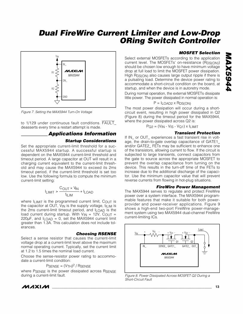
MOSFET SelectionSelect external MOSFETs according to the applicationcurrent level. The MOSFETs’ on-resistance (RDS(ON))should be chosen low enough to have minimum voltagedrop at full load to limit the MOSFET power dissipation.High RDS(ON) also causes large output ripple if there isa pulsating load. Determine the device power rating toaccommodate a short-circuit condition on the board, atstartup, and when the device is in autoretry mode.During normal operation, the external MOSFETs dissipatelittle power. The power dissipated in normal operation is:
P = ILOAD2 x RDS(ON)The most power dissipation will occur during a short-circuit event, resulting in high power dissipated in Q2(Figure 8) during the timeout period for the MAX5944,where the power dissipated across Q2 is:
PQ2 = (VIN - VIS - VQ1) x ILIMIT
Transient ProtectionIf IN_ or OUT_ experiences a fast transient rise in volt-age, the drain-to-gate overlap capacitance of GATE1_and/or GATE2_ FETs may be sufficient to enhance oneof the transistors, allowing current to flow. If the circuit issubjected to large transients, connect capacitors fromthe gate to source across the appropriate MOSFET toprevent the overlap capacitance from turning on thedevice. This results in the turn-off time of the FETs toincrease due to the additional discharge of the capaci-tor. Use the minimum capacitor value that will preventreverse currents from flowing in hot-plug situations.
FireWire Power ManagementThe MAX5944 serves to regulate and protect FireWirepower over a system interface. The MAX5944 program-mable features that make it suitable for both power-provider and power-receiver applications. Figure 9shows a high-end two-port FireWire power-manage-ment system using two MAX5944 dual-channel FireWirecurrent-limiting ICs.
IC V
tILIMIT
OUT IN
ILIMLOAD> +
×
Figure 7. Setting the MAX5944 Turn-On Voltage
MAX5944
R2
R1
VIN
IN_
GND
ON_
VQ1 VQ2VIS
SENSE_ GATE1_ GATE2_ OUT_IN_
+ - + - + -VIN
MAX5944
ILIMIT
Q1 Q2
Figure 8. Power Dissipated Across MOSFET Q2 During aShort-Circuit Fault

MA
X5
94
4
Dual FireWire Current Limiter and Low-Drop ORing Switch Controller
14 ______________________________________________________________________________________
Chip InformationTRANSISTOR COUNT: 4,648
PROCESS: BiCMOS
SENSEA GATE1A GATE2A OUTAINAONA
ONQ1
GND
ONB
RSENSEA Q1A Q2A
RSENSEBQ1B Q2B
TO FireWirePORT 0
SENSEB GATE1B GATE2B OUTBINB
MAX5944
FAULTA
FAULTB
POWER SOURCE
TO FireWirePORT 1
TO FireWirePORT 0
TO FireWirePORT 1
POWER SOURCE
EQUIVALENT CIRCUIT
VERY-LOW-DROPORing DIODE
CURRENT-LIMIT/CIRCUIT-BREAKERAND INRUSH CONTROL
LOAD DISCONECTSWITCH
Typical Operating Circuit
15mΩ IRF7478 IRF7478
SENSEA GATE1A GATE2A OUTAINAONA
ONQ1
GND
ONB
FAULTA
FAULTB
30mΩ IRF7478 IRF7478
30mΩ IRF7478 IRF7478
MAX5035
SGND
VIN
ON
FB
GNDVD
IN4148 IN4148
IN4148
BST
LXPHY
POWER OUT
CABLEON
NOTSLEEP
CURRENT-LIMITSENSE
PORT 1SENSE
PORT 0SENSE
CABLEPOWER
SOURCE
BATTERY-POWERSOURCE
IN4148
CPA SENSE
PORT 0
PORT 1
SENSEB GATE1B GATE2B OUTBINB
SENSEA GATE1A GATE2A OUTAINAONA
ONQ1
GND
ONB
FAULTA
FAULTB
15mΩ IRF7478 IRF7478
SENSEB GATE1B GATE2B OUTBINB
MAX5944 MAX5944
Figure 9. Two-Port FireWire Power Provider

MA
X5
94
4
Dual FireWire Current Limiter and Low-Drop ORing Switch Controller
Maxim cannot assume responsibility for use of any circuitry other than circuitry entirely embodied in a Maxim product. No circuit patent licenses areimplied. Maxim reserves the right to change the circuitry and specifications without notice at any time.
Maxim Integrated Products, 120 San Gabriel Drive, Sunnyvale, CA 94086 408-737-7600 ____________________ 15
© 2004 Maxim Integrated Products Printed USA is a registered trademark of Maxim Integrated Products.
Package Information(The package drawing(s) in this data sheet may not reflect the most current specifications. For the latest package outline informationgo to www.maxim-ic.com/packages.)
SO
ICN
.EP
S
PACKAGE OUTLINE, .150" SOIC
11
21-0041 BREV.DOCUMENT CONTROL NO.APPROVAL
PROPRIETARY INFORMATIONTITLE:
TOP VIEW
FRONT VIEW
MAX
0.0100.069
0.019
0.157
0.010
INCHES
0.150
0.007
E
C
DIM
0.0140.004
BA1
MIN0.053A
0.19
3.80 4.00
0.25
MILLIMETERS
0.100.35
1.35MIN
0.490.25
MAX1.75
0.0500.016L 0.40 1.27
0.3940.386DD
MINDIMD
INCHESMAX
9.80 10.00
MILLIMETERS
MIN MAX
16 AC0.337 0.344 AB8.758.55 140.189 0.197 AA5.004.80 8
N MS012
N
SIDE VIEW
H 0.2440.228 5.80 6.20
e 0.050 BSC 1.27 BSC
C
HE
e B A1
A
D
0∞-8∞L
1VARIATIONS: