Embed Size (px)
Citation preview
General DescriptionThe DS1870 is a dual-channel bias controller targetedtoward class AB LDMOS RF power-amplifier applica-tions. It uses lookup tables (LUTs) to control 256-posi-t ion potentiometers based on the amplif ier’stemperature and drain voltage or current (or otherexternal monitored signal). With its internal temperaturesensor and multichannel A/D converter (ADC), theDS1870 provides a cost-effective solution that improvesthe amplifier’s efficiency by using nonlinear compensa-tion schemes that are not possible with conventionalbiasing solutions.
ApplicationsCellular Base Stations
Medical Equipment
Industrial Controls
Optical Transceivers
Features♦ Two-Channel Solution for Programmable RF Bias
Control♦ The Potentiometer’s Position is Automatically
Updated to Compensate for the AmbientTemperature and the Drain Voltage or Current
♦ A Five-Channel, 13-Bit ADC ContinuouslyMonitors the Ambient Temperature, VCC, VD, ID1,and ID2
♦ Hi/Lo Alarms for Each ADC Channel can Trigger aFault Output
♦ Nonvolatile Memory for the Device Settings,Lookup Tables, and 32-Bytes of User Memory
♦ I2C-Compatible Serial Interface with Up to EightDevices on the Same Serial Bus
♦ Single 5V Power Supply♦ Small 16-Pin TSSOP Package♦ -40°C to +95°C Operational Temperature Range
DS
18
70
LDMOS RF Power-Amplifier Bias Controller
______________________________________________ Maxim Integrated Products 1
TSSOP (173 mils)
1
2
3
4
5
6
7
8 9
10
11
12
13
14
15
16L1
TOP VIEW
W1
W2
L2
ID1
ID2
VD
GND FAULT
A0
A1
A2
SCL
SDA
HCOM
VCC
DS1870
Pin Configuration
Ordering Information
Rev 2; 2/06
For pricing, delivery, and ordering information, please contact Maxim/Dallas Direct! at 1-888-629-4642, or visit Maxim’s website at www.maxim-ic.com.
EVALUATION KIT
AVAILABLE
PART TEMP RANGE PIN-PACKAGE
DS1870E-010 -40°C to +95°C 16 TSSOP (173 mils)
DS1870E-010+ -40°C to +95°C 16 TSSOP (173 mils)
+Denotes lead-free package.
Typical Operating Circuit appears at end of data sheet.

DS
18
70
LDMOS RF Power-Amplifier Bias Controller
2 _____________________________________________________________________
ABSOLUTE MAXIMUM RATINGS
RECOMMENDED DC OPERATING CONDITIONS(TA = -40°C to +95°C)
Stresses beyond those listed under “Absolute Maximum Ratings” may cause permanent damage to the device. These are stress ratings only, and functionaloperation of the device at these or any other conditions beyond those indicated in the operational sections of the specifications is not implied. Exposure toabsolute maximum rating conditions for extended periods may affect device reliability.
Voltage Range on VCC, HCOM, SDA, and SCL Pins Relative toGround ...............................................................-0.5V to +6.0V
Voltage Range on A0, A1, A2, FAULT, VD, ID1, ID2 Relative toGround. ...................-0.5V to VCC + 0.5V, not to exceed +6.0V
Voltage Range on L0, L1, W0, and W1 Relative to Ground .................-0.5V to HCOM + 0.5V, not to exceed +6.0V
Operating Temperature Range ...........................-40°C to +95°CEEPROM Programming Temperature Range .........0°C to +70°CStorage Temperature Range .............................-55°C to +125°CSoldering Temperature .......................................See IPC/JEDEC
J-STD-020A Specification
PARAMETER SYMBOL CONDITIONS MIN TYP MAX UNITS
Supply Voltage VCC (Note 1) 4.5 5.5 V
Input Logic 1(SDA, SCL, A2, A1, A0)
VIH0.7 xVCC
VCC +0.3
V
Input Logic 0(SDA, SCL, A2, A1, A0)
VIL -0.3+0.3 xVCC
V
HCOM Voltage 4.5 5.5 V
LX and WX Voltage -0.3HCOM+ 0.3
V
Wiper Current -1 +1 mA
DC ELECTRICAL CHARACTERISTICS(VCC = +4.5 to 5.5V, TA = -40°C to +95°C.)
PARAMETER SYMBOL CONDITIONS MIN TYP MAX UNITSSupply Current ICC (Note 2) 1 2 mA
Input Leakage ILI -200 +200 nA
VOL1 3mA sink current 0.4 VLow-Level Output Voltage(SDA, FAULT) VOL2 6mA sink current 0.6 V
I/O Capacitance CI/O 10 pF
Digital Power-On Reset VPOD 1.0 2.2 V
Analog Power-On Reset VPOA 2.0 2.8 V

DS
18
70
LDMOS RF Power-Amplifier Bias Controller
_____________________________________________________________________ 3
ANALOG VOLTAGE-MONITORING CHARACTERISTICS(VCC = +4.5 to 5.5V, TA = -40°C to +95°C.)
PARAMETER SYMBOL CONDITIONS MIN TYP MAX UNITS
VD Monitor Factory-Calibrated FS
Code FFF8h 2.488 2.500 2.513 V
VCC Monitor Factory-Calibrated FS
Code FFF8h 6.521 6.553 6.587 V
ID1 and ID2 Monitor Factory-Calibrated FS
Code FFF8h 0.4975 0.5000 0.5025 V
Resolution(VCC, VD, ID1, ID2)
0.0122 %FS
Accuracy(VCC, VD, ID1, ID2)
0.25 0.5 %FS
Update Rate forVCC, VD, ID1, ID2
tframe 50 ms
DIGITAL THERMOMETER CHARACTERISTICS(VCC = +4.5 to 5.5V, TA = -40°C to +95°C.)
PARAMETER SYMBOL CONDITIONS MIN TYP MAX UNITS
Thermometer Error TERR -40°C to 95°C -3 +3 °C
Update Rate tframe 50 ms
ANALOG POTENTIOMETER CHARACTERISTICS(VCC = +4.5 to 5.5V, TA = -40°C to +95°C.)
PARAMETER SYMBOL CONDITIONS MIN TYP MAX UNITSWiper Resistance +25°C 500 1000 Ω
PotentiometerEnd-to-End Resistance
RPOT +25°C 10.0 13 16.8 kΩ
Resolution 0.4 %FS
Absolute Linearity (Note 3) -1 +1 LSB
Relative Linearity (Note 4) -0.5 +0.5 LSB
Ratiometric TemperatureCoefficient
5 ppm/°C
End-to-End TemperatureCoefficient
70 ppm/°C
-3dB Cutoff Frequency (Note 5) 1 MHz
Series Resistors from L1, L2 toGND
RS +25°C 15.1 19.5 25.2 kΩ
VHCOM/VLX 0.5975 0.6 0.6025

DS
18
70
LDMOS RF Power-Amplifier Bias Controller
4 _____________________________________________________________________
LOOKUP TABLE CHARACTERISTICS(VCC = +4.5 to 5.5V, TA = -40°C to +95°C.)
PARAMETER SYMBOL CONDITIONS MIN TYP MAX UNITS
POT1 and POT2 Temp LUT Size 72Byteseach
POT1 and POT2 Temp LUT IndexRange
-40 +102 °C
Temp Step 2 °C
Temp Hysteresis (Note 6) 1 °C
POT1 and POT2 Drain LUT Size 64Byteseach
POT1 and POT2 Drain LUT VDIndex Range
8000 FE00 Hex
POT1 and POT2 Drain LUT VDStep
0200 Hex
POT1 and POT2 Drain LUT VDHysteresis
(Note 6) 0100 Hex
POT1 and POT2 Drain LUT IDXIndex Range
0000 7E00 Hex
POT1 and POT2 Drain LUT IDXStep
0200 Hex
POT1 and POT2 Drain LUT IDXHysteresis
(Note 6) 0100 Hex

DS
18
70
LDMOS RF Power-Amplifier Bias Controller
_____________________________________________________________________ 5
AC ELECTRICAL CHARACTERISTICS (VCC = +4.5V to 5.5V, TA = -40°C to +95°C, timing referenced to VIL(MAX) and VIH(MIN).) (Figure 3)
PARAMETER SYMBOL CONDITIONS MIN TYP MAX UNITSSCL Clock Frequency fSCL (Note 7) 0 400 kHzBus Free Time Between Stop andStart Conditions
tBUF 1.3 µs
Hold Time (Repeated) StartCondition
tHD:STA 0.6 µs
Low Period of SCL tLOW 1.3 µsHigh Period of SCL tHIGH 0.6 µsData Hold Time tHD:DAT 0 0.9 µsData Setup Time tSU:DAT 100 nsStart Setup Time tSU:STA 0.6 µs
SDA and SCL Rise Time tR (Note 8)20 +
0.1CB300 ns
SDA and SCL Fall Time tF (Note 8)20 +
0.1CB300 ns
Stop Setup Time tSU:STO 0.6 µsSDA and SCL CapacitiveLoading
CB (Note 8) 400 pF
EEPROM Write Time tW (Note 9) 10 20 ms
NONVOLATILE MEMORY CHARACTERISTICS(VCC = +4.5V to 5.5V, TA = 0°C to +70°C.)
PARAMETER SYMBOL CONDITIONS MIN TYP MAX UNITS
Writes +70°C (Note 5) 50,000
Note 1: All voltages referenced to ground.Note 2: Supply current is measured with all logic inputs at their inactive state (SDA = SCL = VCC) and driven to well-defined logic
levels. All outputs are disconnected.Note 3: Absolute linearity is the difference of measured value from expected value at the DAC position. Expected value is a
straight line from measured minimum position to measured maximum position.Note 4: Relative linearity is the deviation of an LSB DAC setting change vs. the expected LSB change. Expected LSB change is
the slope of the straight line from measured minimum position to measured maximum position.Note 5: This parameter is guaranteed by design.Note 6: See Figure 1.Note 7: I2C interface timing shown is for fast-mode (400kHz) operation. This device is also backward compatible with I2C stan-
dard-mode timing.Note 8: CB—total capacitance of one bus line in picofarads.Note 9: EEPROM write begins after a stop condition occurs.

DS
18
70
LDMOS RF Power-Amplifier Bias Controller
6 _____________________________________________________________________
Typical Operating Characteristics(VCC = +5.0V, TA = +25°C, unless otherwise noted.)
POTENTIOMETER 1 AND 2 OUTPUT VOLTAGEvs. POSITON
DS18
70 to
c04
WIPER POSITION (DEC)
WIP
ER V
OLTA
GE (V
)
19212864
1
2
3
4
5
6
00 256
HCOM = 5VL1 AND L2 NOT CONNECTED
POTENTIOMETER 1 DIFFERENTIAL NONLINEARITY vs. WIPER POSITION
DS18
70 to
c05
WIPER POSITION (DEC)
DIFF
EREN
TIAL
NON
LINE
ARIT
Y (L
SB)
19212864
-0.20
-0.15
-0.10
-0.05
0
0.05
0.10
0.15
0.20
0.25
-0.250 256
POTENTIOMETER 2 DIFFERENTIAL NONLINEARITY vs. WIPER POSITION
DS18
70 to
c06
WIPER POSITION (DEC)
DIFF
EREN
TIAL
NON
LINE
ARIT
Y (L
SB)
19212864
-0.20
-0.15
-0.10
-0.05
0
0.05
0.10
0.15
0.20
0.25
-0.250 256
POTENTIOMETER 1 INTEGRAL NONLINEARITY vs. WIPER POSITION
DS18
70 to
c07
WIPER POSITION (DEC)
INTE
GRAL
NON
LINE
ARIT
Y (L
SB)
19212864
-0.4
-0.3
-0.2
-0.1
0
0.1
0.2
0.3
0.4
0.5
-0.50 256
POTENTIOMETER 2 INTEGRAL NONLINEARITY vs. WIPER POSITION
DS18
70 to
c08
WIPER POSITION (DEC)
INTE
GRAL
NON
LINE
ARIT
Y (L
SB)
19212864
-0.4
-0.3
-0.2
-0.1
0
0.1
0.2
0.3
0.4
0.5
-0.50 256
POTENTIOMETER 1 AND 2 WIPER RESISTANCE vs. WIPER VOLTAGE
DS18
70 to
c09
WIPER VOLTAGE (V)
WIP
ER R
ESIS
TANC
E (Ω
)
4321
100
200
300
400
500
600
700
800
900
1000
00 5
HCOM = 5.0V
SUPPLY CURRENT vs. SUPPLY VOLTAGE
DS18
70 to
c01
SUPPLY VOLTAGE (V)
SUPP
LY C
URRE
NT (μ
A)
5.35.14.94.7
620
640
660
680
700
720
740
760
780
800
6004.5 5.5
SUPPLY CURRENT vs. TEMPERATURE
DS18
70 to
c02
TEMPERATURE (°C)
SUPP
LY C
URRE
NT (μ
A)
806020 400-20
450
500
550
600
650
700
750
800
850
900
400-40 100
VCC = 5.5V
VCC = 4.5V
VCC = 5.0V
HCOM CURRENT vs. HCOM VOLTAGE
DS18
70 t
oc03
HCOM VOLTAGE (V)
H COM
CUR
RENT
(mA)
5.35.14.94.7
0.05
0.10
0.15
0.20
0.25
0.30
0.35
0.40
0.45
0.50
04.5 5.5

DS
18
70
LDMOS RF Power-Amplifier Bias Controller
_____________________________________________________________________ 7
Typical Operating Characteristics (continued)(VCC = +5.0V, TA = +25°C, unless otherwise noted.)
OUTP
UT D
RIFT
(PPM
/C)
-15
-10
-5
0
5
10
15
20
-20
POTENTIOMETER LOW TERMINAL VOLTAGEvs. TEMPERATURE
DS18
70 to
c12
TEMPERATURE (°C)8060-20 0 20 40-40 100
L1
L2
HCOM = 5.0V
VCC CONVERSION ERRORvs. SUPPLY VOLTAGE
DS18
70 to
c13
SUPPLY VOLTAGE (V)
ERRO
R (%
FS)
5.04.54.03.5
-0.4
-0.3
-0.2
-0.1
0
0.1
0.2
0.3
0.4
0.5
-0.53.0 5.5
DEFAULT VCCCALIBRATION
VD CONVERSION ERRORvs. INPUT VOLTAGE
DS18
70 to
c14
INPUT VOLTAGE (V)
ERRO
R (%
FS)
2.01.51.00.5
-0.4
-0.3
-0.2
-0.1
0
0.1
0.2
0.3
0.4
0.5
-0.50 2.5
DEFAULT VDCALIBRATION
ID1 CONVERSION ERRORvs. INPUT VOLTAGE
DS18
70 to
c15
INPUT VOLTAGE (V)
ERRO
R (%
FS)
0.40.30.20.1
-0.4
-0.3
-0.2
-0.1
0
0.1
0.2
0.3
0.4
0.5
-0.50 0.5
DEFAULT ID1CALIBRATION
ID2 CONVERSION ERRORvs. INPUT VOLTAGE
DS18
70 to
c16
INPUT VOLTAGE (V)
ERRO
R (%
FS)
0.40.30.20.1
-0.4
-0.3
-0.2
-0.1
0
0.1
0.2
0.3
0.4
0.5
-0.50 0.5
DEFAULT ID2CALIBRATION
POTENTIOMETER 1 AND 2 WIPER RESISTANCE vs. WIPER VOLTAGE
DS18
70 to
c09
WIPER VOLTAGE (V)
WIP
ER R
ESIS
TANC
E (Ω
)
4321
100
200
300
400
500
600
700
800
900
1000
00 5
HCOM = 5.0V
POTENTIOMETER 1 AND 2WIPER RESISTANCE vs. TEMPERATURE
DS18
70 to
c10
TEMPERATURE (°C)
RESI
STAN
CE C
HANG
E FR
OM 2
5°C
(PPM
/C)
806020 400-20
100
200
300
400
500
600
700
800
900
1000
0-40 100
HCOM = 5VWIPER VOLTAGE = 4V
POTENTIOMETER END-TO-END RESISTANCEvs. TEMPERATURE
DS18
70 to
c11
TEMPERATURE (°C)
CHAN
GE F
ROM
RES
ISTA
NCE
AT 2
5°C
(PPM
/C)
8060-20 0 20 40
-150
-100
-50
0
50
100
150
200
-200-40 100
RPOT2 + RS2
RPOT1 + RS1

DS
18
70
LDMOS RF Power-Amplifier Bias Controller
8 _____________________________________________________________________
Pin Description
PIN NAME FUNCTION
1 L1 Potentiometer 1 Low Terminal
2 W1 Potentiometer 1 Wiper Terminal
3 W2 Potentiometer 2 Wiper Terminal
4 L2 Potentiometer 2 Low Terminal
5 ID1 Drain Current 1 Monitor Input
6 ID2 Drain Current 2 Monitor Input
7 VD Drain Voltage Monitor Input
8 GND Ground
9 FAULTFault Output. This open-collector output is active high when one of the enabled alarms is outside itsprogrammable limit value.
10 A0
11 A1
12 A2
I2C Address Inputs. These inputs determine the slave address of the device. The slave address inbinary is 1010A2A1A0.
13 SCL Serial Clock Input. I2C clock input.
14 SDA Serial Data Input/Output. Bidirectional I2C data pin.
15 HCOM Potentiometer High Terminal. Common to potentiometers 1 and 2.
16 VCC Power Input
DS
18
70
LDMOS RF Power-Amplifier Bias Controller
_____________________________________________________________________ 9
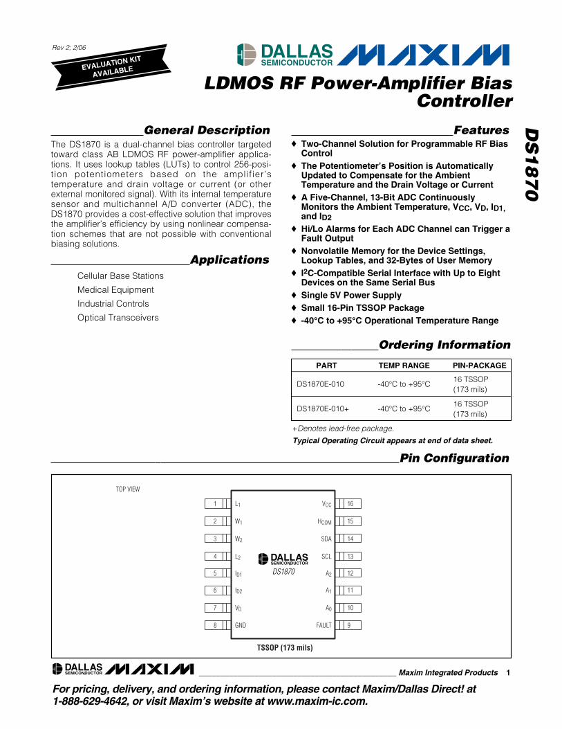
Functional Diagram
∑
∑
++
+
+
∑++ MU
X
13-BITADC
ON-CHIPTEMP SENSOR
VCC
VD
ID1
ID2
ADDRESSGENERATION
SDA
SCL
A0
A1
A2
I2C DATA BUS
32 BYTESUSER
MEMORY OFFSETCALIBRATIONREGISTERS
FAULT
LOADINDEX
INDEX INDEX
INDEX
LOAD
TEMP
POT1RPOT
POT2RPOT
HCOM
L2
W2
W1
L1
POT1DRAIN
LUTTABLE 4
(64 BYTES)
POT2DRAIN
LUTTABLE 5
(64 BYTES) LIMITCOMPARATOR
LIMIT FLAGREGISTERS
FAULTMASK
VCCVCC
GND
GAINCALIBRATIONREGISTERS
VD
VD1 VD2
VD ID2ID1
POT1TEMPLUT
TABLE 2(72 BYTES)
POT2TEMPLUT
TABLE 3(72 BYTES)
RS
RS
I2C INTERFACECONTROL
HI AND LOLIMITS FORTEMP, VCC,VD, ID1, ID2
MEASUREDVALUES FORTEMP, VCC,VD, ID0, ID1
DS1870
DS
18
70
LDMOS RF Power-Amplifier Bias Controller
10 ____________________________________________________________________
Detailed DescriptionThe DS1870 is a dual-channel LDMOS bias controller.It is intended to replace traditional bias control solu-tions that are limited by a constant temperature-coeffi-cient correction. This IC offers lookup table correctionthat is programmable as a function of temperature aswell as drain supply voltage or current. The flexibility touse a nonlinear bias correction improves efficiency sig-nificantly. This is a direct consequence of the ability tolower the bias current, particularly in class AB opera-tion, since the bias correction no longer requires a con-stant temperature coefficient. In addition, correcting thebias as a function of drain supply voltage, or drain cur-rent in class AB, assists in distortion reduction and gainmanagement.
Two outputs (W1 and W2), each controlled by a dedi-cated two-dimensional lookup table as shown in thefunctional diagram, drive two LDMOS gates. The twodegrees of freedom are temperature and either drainsupply voltage or drain current. The lookup tables areprogrammed during power-amplifier assembly andtest. After calibration, the IC automatically recalls theproper control setting for each output, based on tem-perature and drain characteristics.
A 13-bit ADC samples and digitizes the chip tempera-ture, VCC, the drain supply voltage, and two drain cur-rents. These digitized signals are stored in memoryready to be accessed by the look up table controls.The digitized values are also compared to alarmthresholds generating high or low alarm flags. TheFAULT output can be configured to assert high basedany alarm’s assertion, or the alarms can be masked toprevent unwanted fault assertions. The ADC readingsas well as the alarm flags and fault status are accessi-ble through the I2C-compatible interface.
Voltage/Current Monitor OperationThe DS1870 monitors four voltages (VCC, VD, ID1, andID2) plus the temperature in a round-robin fashion usingits 13-bit ADC. The converted voltage values are storedin memory addresses 62h–69h as 16-bit unsignednumbers with the ADC result left justified in the register.
The three least significant bits of the ADC result registersare masked to zero. The round-robin time is specified bytframe in the analog voltage-monitoring characteristics.
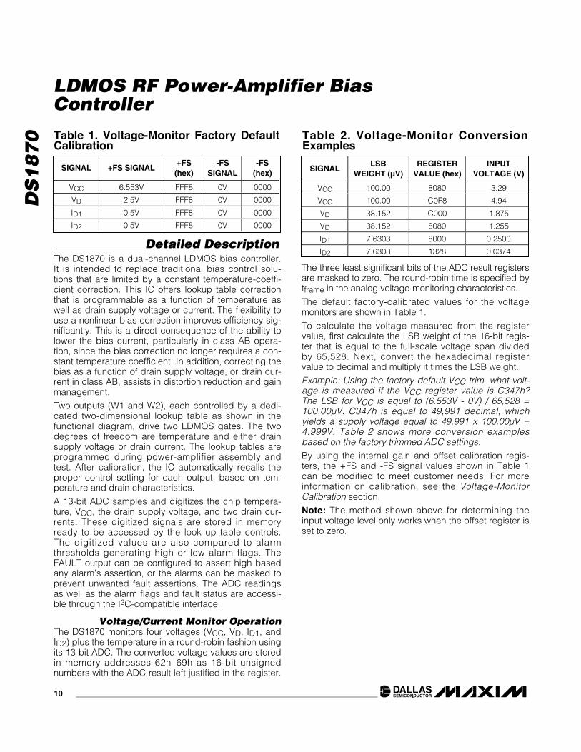
The default factory-calibrated values for the voltagemonitors are shown in Table 1.
To calculate the voltage measured from the registervalue, first calculate the LSB weight of the 16-bit regis-ter that is equal to the full-scale voltage span dividedby 65,528. Next, convert the hexadecimal registervalue to decimal and multiply it times the LSB weight.
Example: Using the factory default VCC trim, what volt-age is measured if the VCC register value is C347h?The LSB for VCC is equal to (6.553V - 0V) / 65,528 =100.00µV. C347h is equal to 49,991 decimal, whichyields a supply voltage equal to 49,991 x 100.00µV =4.999V. Table 2 shows more conversion examplesbased on the factory trimmed ADC settings.By using the internal gain and offset calibration regis-ters, the +FS and -FS signal values shown in Table 1can be modified to meet customer needs. For moreinformation on calibration, see the Voltage-MonitorCalibration section.
Note: The method shown above for determining theinput voltage level only works when the offset register isset to zero.
SIGNAL +FS SIGNAL+FS(hex)
-FSSIGNAL
-FS(hex)
VCC 6.553V FFF8 0V 0000
VD 2.5V FFF8 0V 0000
ID1 0.5V FFF8 0V 0000
ID2 0.5V FFF8 0V 0000
Table 1. Voltage-Monitor Factory DefaultCalibration
SIGNALLSB
WEIGHT (µV)REGISTER
VALUE (hex)INPUT
VOLTAGE (V)
VCC 100.00 8080 3.29
VCC 100.00 C0F8 4.94
VD 38.152 C000 1.875
VD 38.152 8080 1.255
ID1 7.6303 8000 0.2500
ID2 7.6303 1328 0.0374
Table 2. Voltage-Monitor ConversionExamples

DS
18
70
LDMOS RF Power-Amplifier Bias Controller
____________________________________________________________________ 11
Temperature-Monitor OperationThe internal temperature monitor values are stored as 16-bit 2’s complement numbers at memory addresses60h to 61h. The round-robin update time (tframe) for thetemperature register is the same as the voltage moni-tors. The factory default calibration values for the tem-perature monitor are shown in Table 3.
To convert the 2’s complement register value to thetemperature it represents, first convert the 2-byte hexa-decimal value to a decimal value as if it is an unsignedvalue, then divide the result by 256. Finally, subtract256 if the result of the division is greater than or equalto +128. Table 4 shows example converted values.
The offset of the temperature sensor can be adjustedusing the internal calibration registers to account fordifferences between the ambient temperature at thelocation of the DS1870 and the temperature of thedevice it is biasing. When offsets are applied to thetemperature measurement, the value converted will beoff by a fixed value from the DS1870’s ambient temper-ature. For more information, see the TemperatureMonitor Offset Calibration section.
Potentiometer OperationBoth of the DS1870’s potentiometers are 256 positionswith their high terminals connected to the high commonpin, HCOM. The low terminals of the potentiometers areinternally shunted to GND by resistors such that theoutput voltage is 3V to 5V when HCOM is connected toa 5V source. The internal shunt resistors and the poten-tiometer’s end-to-end resistance feature matching tem-perature coefficients that prevent the output voltagefrom drifting over temperature.
External resistors can be placed from HCOM to LX and/orfrom LX to GND to modify the typical output voltage.
Normal OperationDuring normal operation, each potentiometer’s positionis automatically adjusted to the sum of its temperatureand drain LUT values after each round of conversions.The potentiometer setting is applied after both the baseand offset LUT values are recalled from memory. Thesum of the currently indexed values in the POT1 TempLUT (memory table 2) and the POT1 Drain LUT (memo-ry table 4) control potentiometer 1. The sum of the cur-rently indexed values in the POT2 Temp LUT (memory
table 3) and the POT2 Drain LUT (memory table 5) con-trol potentiometer 2. In the event that two table valuesare summed and the result is greater than 255 or lessthan 0, the potentiometer’s position is set to 255 or 0,respectively.
SIGNAL+FS
SIGNAL+FS(hex)
-FSSIGNAL
-FS(hex)
Temp +127.97°C 7FF8 -128.00°C 8000
Table 3. Internal Temperature-MonitorFactory Default Calibration
MSB(bin)
LSB(bin)
TEMPERATURE(°C)
01000000 00000000 +64
01000000 00001111 +64.059
01011111 00000000 +95
11110110 00000000 -10
11011000 00000000 -40
Table 4. Temperature Conversion Values
LUT ADDRESS (hex)CORRESPONDING
TEMPERATURE (°C)
80 ≤ -40°C
81 -38°C
82 -36°C
… …
C6 +100°C
C7 ≥ +102°C
Table 5. LUT Addresses forCorresponding Temperature Values
DS
18
70
LDMOS RF Power-Amplifier Bias Controller
12 ____________________________________________________________________
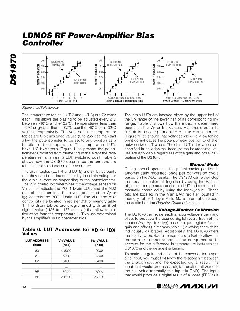
The temperature tables (LUT 2 and LUT 3) are 72 byteseach. This allows the biasing to be adjusted every 2°Cbetween -40°C and +102°C. Temperatures less than-40°C or greater than +102°C use the -40°C or +102°C values, respectively. The values in the temperaturetables are 8-bit unsigned values (0 to 255 decimal) thatallow the potentiometer to be set to any position as afunction of the temperature. The temperature LUTshave 1°C hysteresis (Figure 1) to prevent the poten-tiometer’s position from chattering in the event the tem-perature remains near a LUT switching point. Table 5shows how the DS1870 determines the temperaturetables index as a function of temperature.
The drain tables (LUT 4 and LUT5) are 64 bytes each,and they can be indexed either by the drain voltage orthe drain current corresponding to the potentiometer.The VD1 control bit determines if the voltage sensed onVD or ID1 adjusts the POT1 Drain LUT, and the VD2control bit determines if the voltage sensed on VD orID2 controls the POT2 Drain LUT. The VD1 and VD2control bits are located in register 85h of memory table1. The drain tables are programmed with an 8-bitsigned value (-128 to +127 decimal) that allow a rela-tive offset from the temperature LUT values determinedby the amplifier’s drain characteristics.
The drain LUTs are indexed either by the upper half ofthe VD range or the lower half of its corresponding IDXrange. Table 6 shows how the index is determinedbased on the VD or IDX values. Hysteresis equal to0100h is also implemented on the drain monitor (Figure 1) to ensure that voltages close to a switchingpoint do not cause the potentiometer position to chatterbetween two LUT values. The drain LUT index values arespecified in hexadecimal because the hexadecimal val-ues are applicable regardless of the gain and offset cali-bration of the DS1870.
Manual ModeDuring normal operation, the potentiometer position isautomatically modified once per conversion cyclebased on the ADC results. The DS1870 can either stopthe update function all together by using the B/O_enbit, or the temperature and drain LUT indexes can bemanually controlled by using the Index_en bit. Thesebits are located in the Man DAC register located inmemory table 1, byte AFh. More information aboutthese bits is in the Register Description section.
Voltage-Monitor CalibrationThe DS1870 can scale each analog voltage’s gain andoffset to produce the desired digital result. Each of theinputs (VCC, VD, ID1, ID2) has a unique register for thegain and offset (in memory table 1) allowing them to beindividually calibrated. Additionally, the DS1870 offersthe ability to provide a temperature offset to allow thetemperature measurement to be compensated toaccount for the difference in temperature between theDS1870 and the device it is biasing.
To scale the gain and offset of the converter for a spe-cific input, you must first know the relationship betweenthe analog input and the expected digital result. Theinput that would produce a digital result of all zeros isthe null value (normally this input is GND). The inputthat would produce a digital result of all ones (FFF8h) is
LUT ADDRESS(hex)
VD VALUE(hex)
IDX VALUE(hex)
80 ≤ 8000 0000
81 8200 0200
82 8400 0400
… … …
BE FC00 7C00
BF ≥ FE00 ≥ 7E00
Table 6. LUT Addresses for VD or IDXValues
9Ah
99h
98h
97h
96h
95h
2 4 6 8 10 12TEMPERATURE (°C)
MEM
ORY
LOCA
TION
MEM
ORY
LOCA
TION
MEM
ORY
LOCA
TION
9Ah
99h
98h
97h
96h
95h
AA00 AC00AEOO B000 B200 B400DRAIN VOLTAGE CONVERSION (HEX)
9Ah
99h
98h
97h
96h
95h
2A00 2C00 2E00 3000 3200 3400DRAIN CURRENT CONVERSION (HEX)
INCREASINGTEMPERATURE
INCREASINGDRAIN VOLTAGE
INCREASINGDRAIN CURRENT
DECREASINGTEMPERATURE
DECREASINGDRAIN VOLTAGE
DECREASINGDRAIN CURRENT
Figure 1. LUT Hysteresis
DS
18
70
LDMOS RF Power-Amplifier Bias Controller
____________________________________________________________________ 13
the full-scale (FS) value. The expected FS value is alsofound by multiplying an all-ones digital answer by theLSB weight.
Example: Since the FS digital reading is 65,528 (FFF8hex) LSBs, if the LSB’s weight is 50µV, then the FSvalue is 65,528 x 50µV = 3.2764V.
A binary search is used to calibrate the gain of the con-verter. This requires forcing two known voltages to theinput pin. It is preferred that one of the forced voltagesis the null input and the other is 90% of FS. Since theLSB of the least significant bit in the digital reading reg-ister is known, the expected digital results can be cal-culated for both the null input and the 90% of full scalevalue.
An explanation of the binary search used to scale thegain is best served with the following example pseudo-code:/* Assume that the null input is 0.5V *//* Assume that the requirement for the LSB is 50µV */
FS = 65528 * 50e-6; /*3.2764V */CNT1 = 0.5 / 50e-6; /* 1000 */CNT2 = 0.9 X FS / 50e-6; /* 58981.5 */
/* So the null input is 0.5V and 90% of FS is 2.949V */
Set the input’s offset register to zerogain_result = 0h; /* Working register for gain
calculation */CLAMP = FFF8h; /* This is the max ADC value*/For n = 15 down to 0begin
gain_result = gain_result + 2n;Write gain_result to the input’s gain register;Force the 90% FS input (2.949V);Meas2= ADC result from DS1870;If Meas2 ≥ CLAMPThengain_result = gain_result - 2n;ElseForce the null input (0.5V)Meas1 = ADC result from DS1870If [(Meas2-Meas1)>(CNT2-CNT1)]Thengain_result = gain_result - 2n;
end;Write gain_result to the input’s gain register;
The gain register is now set and the resolution of theconversion matches the expected LSB. Customers
requiring non-zero null values (e.g., 0.5V) must nextcalibrate the input’s offset. If the desired null value is0V, leave the offset register programmed to 0000h andskip this step.
To calibrate the offset register, program the gain regis-ter with the gain_result value determined above. Next,force the null input voltage (0.5V for the example) andread the digital result from the part (Meas1). The offsetvalue can be calculated using the following formula:
Temperature-Monitor Offset CalibrationThe DS1870’s temperature sensor comes precalibratedand requires no further adjustment by the customer forproper operation. However, it is possible for customersto characterize their system and add a fixed offset tothe DS1870’s temperature reading so it is reflective ofanother location’s temperature. This is not required forbiasing because the temperature offset can beaccounted for by adjusting the data’s location in theLUTs, but this feature is available for customers whosee application benefits.
To change the temperature sensor’s offset: write thetemperature offset register to 0000h, measure thesource reference temperature (Tref), and read the tem-perature from the DS1870 (TDS1870). Then, the follow-ing formula can be used to calculate the value for thetemperature offset register.
Once the value is calculated, write it to the temperatureoffset register.
Power-Up and Low-Voltage OperationDuring power-up, the device is inactive until VCCexceeds the digital power-on-reset voltage (VPOD). Atthis voltage, the digital circuitry, which includes the I2C-compatible interface, becomes functional. However,EEPROM-backed registers/settings cannot be internallyread (recalled) until VCC exceeds the analog power-onreset (VPOA), at which time the remainder or the devicebecomes fully functional. Once VCC exceeds VPOA, theRdyb bit in byte 74h is timed to go from a 1 to a 0 andindicates when ADC conversions begin. If VCC everdips below VPOA, the Rdyb bit reads as a 1 again.Once a device exceeds VPOA and the EEPROM isrecalled, the values remain active (recalled) until VCCfalls below VPOD.
TempOffset T T XOR BB href DS bitwise= × − + −( )( )64 275 401870
OffsetMeas= − × ⎛
⎝⎜⎞⎠⎟
11
4

DS
18
70
LDMOS RF Power-Amplifier Bias Controller
14 ____________________________________________________________________
As the device powers up, the VCC Lo alarm flagdefaults to a 1 until the first VCC ADC conversionoccurs and sets or clears the flag accordingly. TheFAULT output is active when VCC < VPOA.
Memory DescriptionThe DS1870 memory map is divided into six sectionsthat include the lower memory (addresses 00h to 7Fh)and five memory tables (Figure 2). The memory tablesare addressed by setting the table-select byte (7Fh) tothe desired table number and accessing the uppermemory locations (80h to FFh). The lower memory canbe addressed at any time regardless of the state of thetable-select byte. The lower memory and memory table1 are used to configure the DS1870 and read the statusof the monitors. The lower memory also contains the 32bytes of user memory. Memory tables 2 and 3 containthe base potentiometer positions that are used for bias-ing based on the reading of the internal temperaturesensor. Memory tables 4 and 5 contain the relative off-sets that are added to the base number as a function ofeither the drain voltage or the individual drain currentmonitors. See the Memory Map for a complete listing ofregisters and the Register Description section fordetails about each register.
Password Memory ProtectionThe DS1870 contains a 2-byte password that allows allof its EE memory to be write protected until the properpassword is entered into the password entry (PWE)word (address 78h). This allows factory calibration datafor the bias settings, alarm thresholds, and all the otherEEPROM information to be write protected. The pass-word is set by writing to the Password register, which isthe first two bytes of memory table 1.
The factory default value for the password is FFFFh,which is also the factory default value for PWE onpower-up. This means that parts are unlocked at
power-up when they are first received by customers.The password should be programmed to a value otherthan FFFFh to ensure the calibration data is write pro-tected. The PWE register always reads 0000h regard-less of its programmed value.
EEPROM Write DisableMemory locations 20h to 3Fh and Table 1 locations 80hto A7h are SRAM-shadowed EEPROM. By default (SEE = 0) these locations act as ordinary EEPROM. Bysetting SEE = 1, these locations begin to function likeSRAM cells, which allow an infinite number of writecycles without concern of wearing out the EEPROM.This also eliminates the requirement for the EEPROMwrite time. Because changes made with SEE = 1 do notaffect the EEPROM, these changes are not retainedthrough power cycles. The power-up value is the lastvalue written with SEE = 0. This function can be used tolimit the number of EEPROM writes during calibration orto change the monitor thresholds periodically duringnormal operation without wearing out the EEPROM. TheSEE bit resides in memory table 1, byte AFh.
Memory MapThe upper part of the memory map is organized into 8-byte or 4-word (2-byte) rows. The beginning addressof the row is shown in the left-most column of the map,and is equal to the byte 0 or word 0 memory address.The next byte (Byte 1) is located at the next highestmemory address, and the next word (Word 1) is twomemory addresses greater than the row’s beginningaddress. The lower part of the memory map expandsthe bytes or the words to show the names of the bitswithin the byte/word, or their bit weights (2X) for regis-ters that contain numerical information. Numerical reg-isters that contain an “S” in the most significant bit areshowing sign extension for 2’s complement numbers.Descriptions of each byte/bit follow in the RegisterDescription section.
USER MEMORY;HI/LO ALARMTHRESHOLDS;ADC RESULTS;
CONFIGURATION
CONFIGURATION POT1TEMPLUT
POT2TEMPLUT
POT1DRAIN
LUT
POT2DRAIN
LUT
00h
7Fh
80h
AFh
80h
C7h
80h
C7h
80h
BFh
80h
BFh
MAIN MEMORYTABLE 1 TABLE 2 TABLE 3 TABLE 4 TABLE 5
TABLE-SELECTBYTE (7Fh)
SELSEL SEL
SEL SEL
Figure 2. Memory Organization

DS
18
70
LDMOS RF Power-Amplifier Bias Controller
____________________________________________________________________ 15
LOWER MEMORY
WORD 0 WORD 1 WORD 2 WORD 3ROW(HEX)
ROWNAME BYTE 0 BYTE 1 BYTE 2 BYTE 3 BYTE 4 BYTE 5 BYTE 6 BYTE 7
00 User Row0 User EE User EE User EE User EE User EE User EE User EE User EE
08 User Row1 User EE User EE User EE User EE User EE User EE User EE User EE
10 User Row2 User EE User EE User EE User EE User EE User EE User EE User EE
18 User Row3 User EE User EE User EE User EE User EE User EE User EE User EE
20 Threshold0 Temp Hi Alarm VCC Hi Alarm VD Hi Alarm ID1 Hi Alarm
28 Threshold1 ID2 Hi Alarm Reserved Reserved Reserved
30 Threshold2 Temp Lo Alarm VCC Lo Alarm VD Lo Alarm ID1 Lo Alarm
38 Threshold3 ID2 Lo Alarm Reserved Reserved Reserved
40 Reserved Reserved Reserved Reserved Reserved Reserved Reserved Reserved
48 Reserved Reserved Reserved Reserved Reserved Reserved Reserved Reserved
50 Reserved Reserved Reserved Reserved Reserved Reserved Reserved Reserved
58 Reserved Reserved Reserved Reserved Reserved Reserved Reserved Reserved
60 A2D Value0 Temp Value VCC Value VD Value ID1 Value
68 A2D Value1 ID2 Value Reserved Reserved Reserved
70 Status Hi Alarm Lo Alarm Reserved Reserved I/O Status A2D Status Reserved Reserved
78 Table Select PWE Reserved Reserved Reserved Reserved Reserved Tbl Sel
EXPANDED BYTES
BIT 7 BIT 6 BIT 5 BIT 4 BIT 3 BIT 2 BIT 1 BIT 0BYTE(HEX)
BYTENAME BIT15 BIT14 BIT13 BIT12 BIT11 BIT10 BIT9 BIT8 BIT7 BIT6 BIT5 BIT4 BIT3 BIT2 BIT1 BIT0
00-1F User EE EE EE EE EE EE EE EE EE
20 Temp Hi Alrm S 26 25 24 23 22 21 20 2-1 2-2 2-3 2-4 2-5 2-6 2-7 2-8
22 VCC Hi Alrm 215 214 213 212 211 210 29 28 27 26 25 24 23 22 21 20
24 VD Hi Alrm 215 214 213 212 211 210 29 28 27 26 25 24 23 22 21 20
26 ID1 Hi Alrm 215 214 213 212 211 210 29 28 27 26 25 24 23 22 21 20
28 ID2 Hi Alrm 215 214 213 212 211 210 29 28 27 26 25 24 23 22 21 20
30 Temp Lo Alrm S 26 25 24 23 22 21 20 2-1 2-2 2-3 2-4 2-5 2-6 2-7 2-8
32 VCC Lo Alrm 215 214 213 212 211 210 29 28 27 26 25 24 23 22 21 20
34 VD Lo Alrm 215 214 213 212 211 210 29 28 27 26 25 24 23 22 21 20
36 ID1 Lo Alrm 215 214 213 212 211 210 29 28 27 26 25 24 23 22 21 20
38 ID2 Lo Alrm 215 214 213 212 211 210 29 28 27 26 25 24 23 22 21 20
60 Temp Value S 26 25 24 23 22 21 20 2-1 2-2 2-3 2-4 2-5 2-6 2-7 2-8
62 VCC Value 215 214 213 212 211 210 29 28 27 26 25 24 23 22 21 20
64 VD Value 215 214 213 212 211 210 29 28 27 26 25 24 23 22 21 20
66 ID1 Value 215 214 213 212 211 210 29 28 27 26 25 24 23 22 21 20
68 ID2 Value 215 214 213 212 211 210 29 28 27 26 25 24 23 22 21 20
70 Hi Alarm Temp Hi VCC Hi VD Hi ID1 Hi ID2 Hi Reserved Reserved Reserved
71 Lo Alarm Temp Lo VCC Lo VD Lo ID1 Lo ID2 Lo Reserved Reserved Reserved
74 I/O Status Reserved Reserved Reserved Reserved Fault Mint Reserved Rdyb
75 A2D Status Temp Rdy VCC Rdy VD Rdy ID1 Rdy ID2 Rdy Reserved Reserved Reserved
78 PWE 215 214 213 212 211 210 29 28 27 26 25 24 23 22 21 20
7F Tbl Sel 27 26 25 24 23 22 21 20

DS
18
70
LDMOS RF Power-Amplifier Bias Controller
16 ____________________________________________________________________
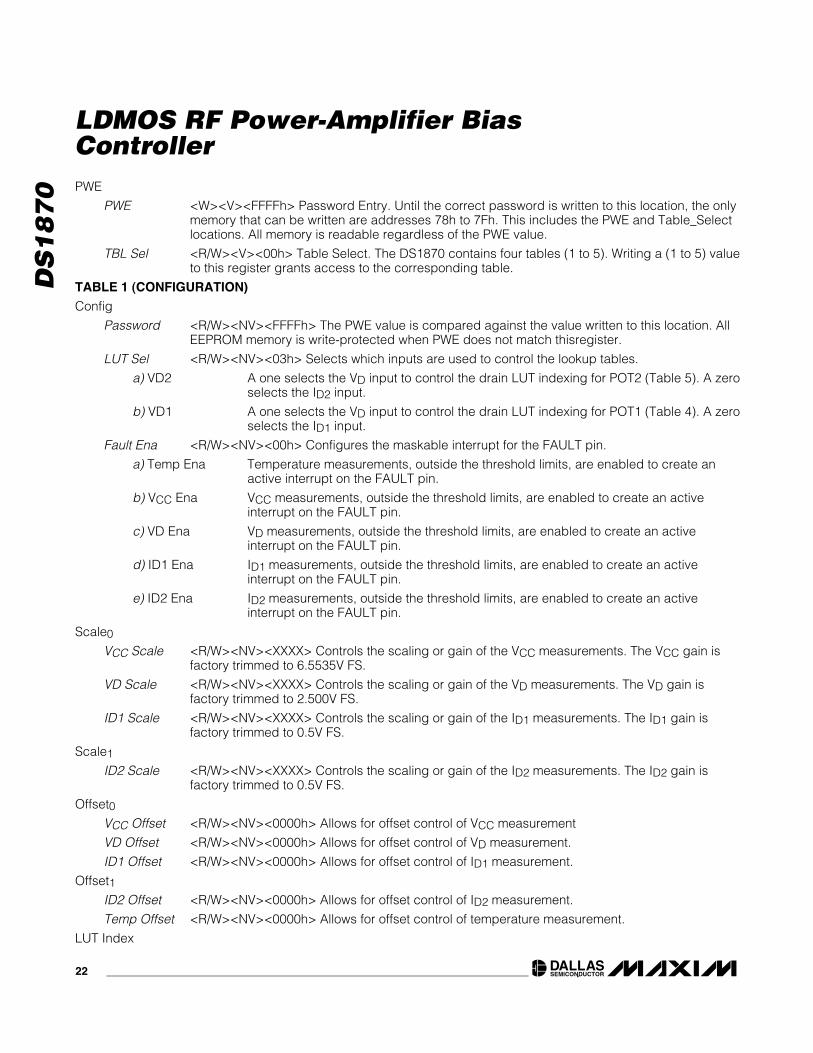
TABLE 1 ( CONFIGURATION )
WORD 0 WORD 1 WORD 2 WORD 3ROW(HEX)
ROWNAME BYTE 0 BYTE 1 BYTE 2 BYTE 3 BYTE 4 BYTE 5 BYTE 6 BYTE 7
80 Config Password LUT Sel Fault Ena Reserved
88 Scale0 Reserved Vcc Scale VD Scale ID1 Scale
90 Scale1 ID2 Scale Reserved Reserved Reserved
98 Offset0 Reserved Vcc Offset VD Offset ID1 offset
A0 Offset1 ID2 Offset Reserved Reserved Temp Offset
A8LUT
IndexT Index O1 Index O2 Index POT1 base POT1 off
POT2base
POT2 off Man Dac
EXPANDED BYTES
BIT 7 BIT 6 BIT 5 BIT 4 BIT 3 BIT 2 BIT 1 BIT 0BYTE(HEX)
BYTENAME BIT15 BIT14 BIT13 BIT12 BIT11 BIT10 BIT9 BIT8 BIT7 BIT6 BIT5 BIT4 BIT3 BIT2 BIT1 BIT0
80 Password 215 214 213 212 211 210 29 28 27 26 25 24 23 22 21 20
85 LUT Sel Reserved Reserved Reserved Reserved Reserved Reserved VD2 VD1
86 Fault Ena Temp Ena Vcc Ena VD Ena ID1 Ena ID2 Ena Reserved Reserved Reserved
8A Vcc 215 214 213 212 211 210 29 28 27 26 25 24 23 22 21 20
8C VD Scale 215 214 213 212 211 210 29 28 27 26 25 24 23 22 21 20
8E ID1 Scale 215 214 213 212 211 210 29 28 27 26 25 24 23 22 21 20
90 ID2 Scale 215 214 213 212 211 210 29 28 27 26 25 24 23 22 21 20
9AVcc
OffsetS S 215 214 213 212 211 210 29 28 27 26 25 24 23 22
9C VD Offset S S 215 214 213 212 211 210 29 28 27 26 25 24 23 22
9E ID1 S S 215 214 213 212 211 210 29 28 27 26 25 24 23 22
A0 ID2 S S 215 214 213 212 211 210 29 28 27 26 25 24 23 22
A6TempOffset
S 28 27 26 25 24 23 22 21 20 2-1 2-2 2-3 2-4 2-5 2-6
A8 T Index 27 26 25 24 23 22 21 20
A9 O1 Index 27 26 25 24 23 22 21 20
AA O2 Index 27 26 25 24 23 22 21 20
ABPOT1base
27 26 25 24 23 22 21 20
AC POT1 off S 26 25 24 23 22 21 20
ADPOT2base
27 26 25 24 23 22 21 20
AE POT2 off S 26 25 24 23 22 21 20
AF Man DAC Reserved Reserved Reserved Reserved Reserved SEE B/O_en index_en

DS
18
70
LDMOS RF Power-Amplifier Bias Controller
____________________________________________________________________ 17
TABLE 2 (POT1 TEMP LUT)
WORD 0 WORD 1 WORD 2 WORD 3ROW(HEX)
ROWNAME BYTE 0 BYTE 1 BYTE 2 BYTE 3 BYTE 4 BYTE 5 BYTE 6 BYTE 7
80 LUT POT1 POT1 POT1 POT1 POT1 POT1 POT1 POT1
88 LUT POT1 POT1 POT1 POT1 POT1 POT1 POT1 POT1
90 LUT POT1 POT1 POT1 POT1 POT1 POT1 POT1 POT1
98 LUT POT1 POT1 POT1 POT1 POT1 POT1 POT1 POT1
A0 LUT POT1 POT1 POT1 POT1 POT1 POT1 POT1 POT1
A8 LUT POT1 POT1 POT1 POT1 POT1 POT1 POT1 POT1
B0 LUT POT1 POT1 POT1 POT1 POT1 POT1 POT1 POT1
B8 LUT POT1 POT1 POT1 POT1 POT1 POT1 POT1 POT1
C0 LUT POT1 POT1 POT1 POT1 POT1 POT1 POT1 POT1
C8 Reserved Reserved Reserved Reserved Reserved Reserved Reserved Reserved
D0 Reserved Reserved Reserved Reserved Reserved Reserved Reserved Reserved
D8 Reserved Reserved Reserved Reserved Reserved Reserved Reserved Reserved
E0 Reserved Reserved Reserved Reserved Reserved Reserved Reserved Reserved
E8 Reserved Reserved Reserved Reserved Reserved Reserved Reserved Reserved
F0 Reserved Reserved Reserved Reserved Reserved Reserved Reserved Reserved
F8 Reserved Reserved Reserved Reserved Reserved Reserved Reserved Reserved
EXPANDED BYTES
BYTE(HEX)
BYTENAME
BIT 7 BIT 6 BIT 5 BIT 4 BIT 3 BIT 2 BIT 1 BIT 0
80-C7 POT1 27 26 25 24 23 22 21 20

DS
18
70
LDMOS RF Power-Amplifier Bias Controller
18 ____________________________________________________________________
TABLE 3 ( POT2 TEMP LUT)WORD 0 WORD 1 WORD 2 WORD 3ROW
(HEX)ROWNAME BYTE 0 BYTE 1 BYTE 2 BYTE 3 BYTE 4 BYTE 5 BYTE 6 BYTE 7
80 LUT POT2 POT2 POT2 POT2 POT2 POT2 POT2 POT2
88 LUT POT2 POT2 POT2 POT2 POT2 POT2 POT2 POT2
90 LUT POT2 POT2 POT2 POT2 POT2 POT2 POT2 POT2
98 LUT POT2 POT2 POT2 POT2 POT2 POT2 POT2 POT2
A0 LUT POT2 POT2 POT2 POT2 POT2 POT2 POT2 POT2
A8 LUT POT2 POT2 POT2 POT2 POT2 POT2 POT2 POT2
B0 LUT POT2 POT2 POT2 POT2 POT2 POT2 POT2 POT2
B8 LUT POT2 POT2 POT2 POT2 POT2 POT2 POT2 POT2
C0 LUT POT2 POT2 POT2 POT2 POT2 POT2 POT2 POT2
C8 Reserved Reserved Reserved Reserved Reserved Reserved Reserved Reserved
D0 Reserved Reserved Reserved Reserved Reserved Reserved Reserved Reserved
D8 Reserved Reserved Reserved Reserved Reserved Reserved Reserved Reserved
E0 Reserved Reserved Reserved Reserved Reserved Reserved Reserved Reserved
E8 Reserved Reserved Reserved Reserved Reserved Reserved Reserved Reserved
F0 Reserved Reserved Reserved Reserved Reserved Reserved Reserved Reserved
F8 Reserved Reserved Reserved Reserved Reserved Reserved Reserved Reserved
EXPANDED BYTES
BYTE(HEX)
BYTENAME
BIT 7 BIT 6 BIT 5 BIT 4 BIT 3 BIT 2 BIT 1 BIT 0
80-C7 POT2 27 26 25 24 23 22 21 20
DS
18
70
LDMOS RF Power-Amplifier Bias Controller
____________________________________________________________________ 19
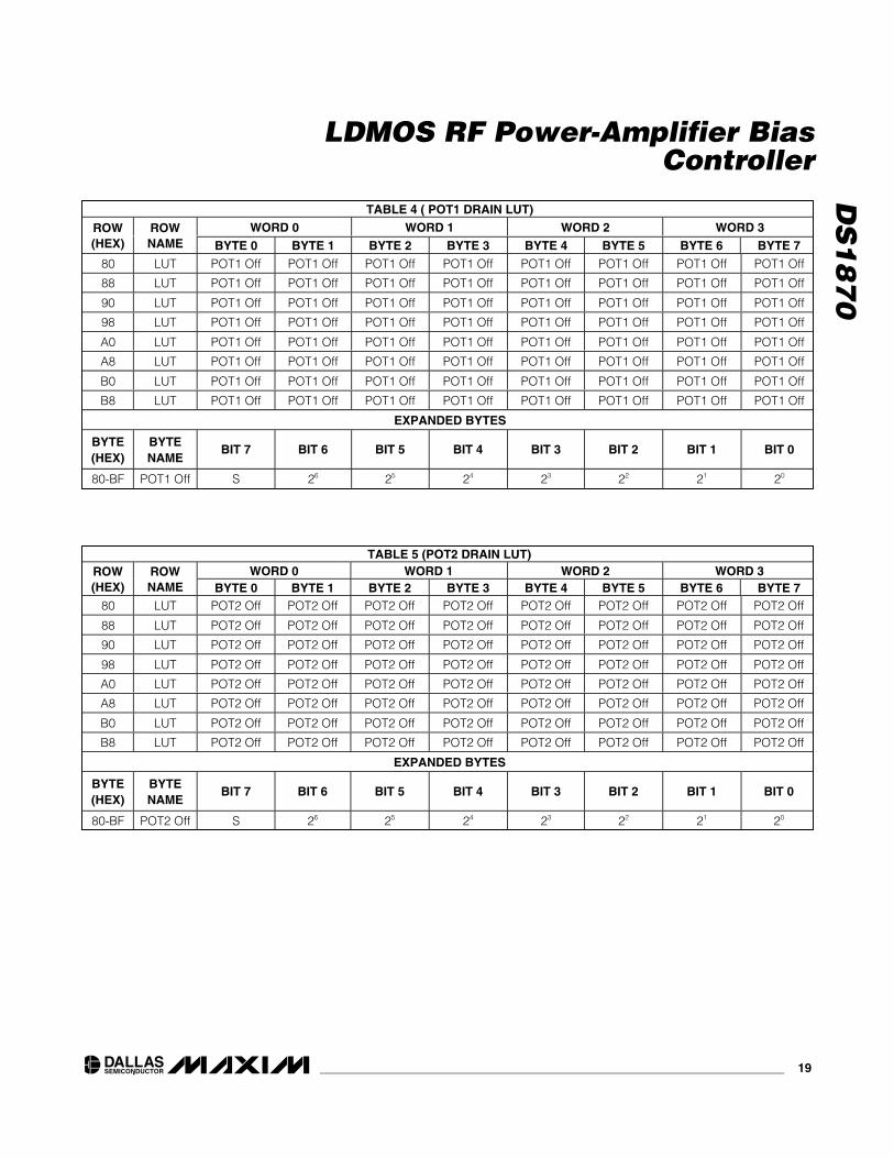
TABLE 4 ( POT1 DRAIN LUT)WORD 0 WORD 1 WORD 2 WORD 3ROW
(HEX)ROWNAME BYTE 0 BYTE 1 BYTE 2 BYTE 3 BYTE 4 BYTE 5 BYTE 6 BYTE 7
80 LUT POT1 Off POT1 Off POT1 Off POT1 Off POT1 Off POT1 Off POT1 Off POT1 Off
88 LUT POT1 Off POT1 Off POT1 Off POT1 Off POT1 Off POT1 Off POT1 Off POT1 Off
90 LUT POT1 Off POT1 Off POT1 Off POT1 Off POT1 Off POT1 Off POT1 Off POT1 Off
98 LUT POT1 Off POT1 Off POT1 Off POT1 Off POT1 Off POT1 Off POT1 Off POT1 Off
A0 LUT POT1 Off POT1 Off POT1 Off POT1 Off POT1 Off POT1 Off POT1 Off POT1 Off
A8 LUT POT1 Off POT1 Off POT1 Off POT1 Off POT1 Off POT1 Off POT1 Off POT1 Off
B0 LUT POT1 Off POT1 Off POT1 Off POT1 Off POT1 Off POT1 Off POT1 Off POT1 Off
B8 LUT POT1 Off POT1 Off POT1 Off POT1 Off POT1 Off POT1 Off POT1 Off POT1 Off
EXPANDED BYTES
BYTE(HEX)
BYTENAME
BIT 7 BIT 6 BIT 5 BIT 4 BIT 3 BIT 2 BIT 1 BIT 0
80-BF POT1 Off S 26 25 24 23 22 21 20
TABLE 5 (POT2 DRAIN LUT)WORD 0 WORD 1 WORD 2 WORD 3ROW
(HEX)ROWNAME BYTE 0 BYTE 1 BYTE 2 BYTE 3 BYTE 4 BYTE 5 BYTE 6 BYTE 7
80 LUT POT2 Off POT2 Off POT2 Off POT2 Off POT2 Off POT2 Off POT2 Off POT2 Off
88 LUT POT2 Off POT2 Off POT2 Off POT2 Off POT2 Off POT2 Off POT2 Off POT2 Off
90 LUT POT2 Off POT2 Off POT2 Off POT2 Off POT2 Off POT2 Off POT2 Off POT2 Off
98 LUT POT2 Off POT2 Off POT2 Off POT2 Off POT2 Off POT2 Off POT2 Off POT2 Off
A0 LUT POT2 Off POT2 Off POT2 Off POT2 Off POT2 Off POT2 Off POT2 Off POT2 Off
A8 LUT POT2 Off POT2 Off POT2 Off POT2 Off POT2 Off POT2 Off POT2 Off POT2 Off
B0 LUT POT2 Off POT2 Off POT2 Off POT2 Off POT2 Off POT2 Off POT2 Off POT2 Off
B8 LUT POT2 Off POT2 Off POT2 Off POT2 Off POT2 Off POT2 Off POT2 Off POT2 Off
EXPANDED BYTES
BYTE(HEX)
BYTENAME
BIT 7 BIT 6 BIT 5 BIT 4 BIT 3 BIT 2 BIT 1 BIT 0
80-BF POT2 Off S 26 25 24 23 22 21 20

DS
18
70
LDMOS RF Power-Amplifier Bias Controller
20 ____________________________________________________________________
Register DescriptionThe register descriptions are organized by the register’s row address starting with the lower memory, then proceed-ing through each lookup table in order. The format of the register description is shown below.
TABLE NAME
Name of Row
Name of Byte <Access><Volatility><Power-On/Factor Default Values> Descriptionof the byte’s function
a) bit X bit X descriptionb) bit Y bit Y description
The Access value following each byte’s name defines the read/write access for the register. Possible values areread-only (R), write-only (W), and read-write (R/W). The Volatility parameter defines if the memory is volatile (V) ornonvolatile (NV). Some registers correspond to values measured or detected by the DS1870. These parameters areread-only and listed as NA since their values are indeterminate. Power-On values are the default states of thevolatile register, and the Factory Default values are the values the EEPROM memory is programmed to by the factory before they are shipped from Dallas Semiconductor.
LOWER MEMORY
User Row
User EE <R/W><NV><00h> NV EEPROM user memory.
Threshold0
Temp Hi Alarm<R/W><NV><0000h> Temperature measurements above this 2’s complement threshold set its corresponding alarm bit. Measurements below this threshold clear the alarm bit.
VCC Hi Alarm <R/W><NV><0000h> Voltage measurements of the VCC input above this unsigned threshold set its corresponding alarm bit. Measurements below this threshold clear the alarm bit.
VD Hi Alarm <R/W><NV><0000h> Voltage measurements of the VD input above this unsigned threshold set its corresponding alarm bit. Measurements below this threshold clear the alarm bit.
ID1 Hi Alarm <R/W><NV><0000h> Voltage measurements of the ID1 input above this unsigned threshold set its corresponding alarm bit. Measurements below this threshold clear the alarm bit.
Threshold1
ID2 Hi Alarm <R/W><NV><0000h> Voltage measurements of the ID2 input above this unsigned threshold setits corresponding alarm bit. Measurements below this threshold clear the alarm bit.
Threshold2
Temp Lo Alarm<R/W><NV><0000h> Temperature measurements below this 2’s complement threshold set its corresponding alarm bit. Measurements above this threshold clear the alarm bit.
VCC Lo Alarm <R/W><NV><0000h> Voltage measurements of the VCC below above this unsigned threshold set its corresponding alarm bit. Measurements above this threshold clear the alarm bit.
VD Lo Alarm <R/W><NV><0000h> Voltage measurements of the VD input below this unsigned threshold set its corresponding alarm bit. Measurements above this threshold clear the alarm bit.
ID1 Lo Alarm <R/W><NV><0000h> Voltage measurements of the ID1 input below this unsigned threshold set its corresponding alarm bit. Measurements above this threshold clear the alarm bit.
Threshold3
ID1 Lo Alarm <R/W><NV><0000h> Voltage measurements of the ID2 input below this unsigned threshold set its corresponding alarm bit. Measurements above this threshold clear the alarm bit.

DS
18
70
LDMOS RF Power-Amplifier Bias Controller
____________________________________________________________________ 21
A2D Value0
Temp Value <R><NA><0000h> The signed 2’s complement direct-to-temperature measurement.
VCC Value <R><NA><0000h> Unsigned VCC voltage measurement.
VD Value <R><NA><0000h> Unsigned VD voltage measurement.
ID1 Value <R><NA><0000h> Unsigned ID1 voltage measurement.
A2D Value1
ID2 Value <R><NA><0000h> Unsigned ID2 voltage measurement.
Status
Hi Alarm <R><NA><00h> High-Alarm Status bits.
a) Temp Hi High-alarm status for temperature measurement.
b) VCC Hi High-alarm status for VCC measurement.
c) VD Hi High-alarm status for VD measurement.
d) ID1 Hi High-alarm status for ID1 measurement.
e) ID2 HI High-alarm status for ID2 measurement.
Lo Alarm <R><NA><40h> Low-Alarm Status bits.
a) Temp Lo Low-alarm status for temperature measurement.
b) VCC Lo Low-alarm status for VCC measurement. This bit is set when the VCC supply is below the POR trip-point value. It clears itself when a VCC measurement is completed and the value is above the low threshold.
c) VD Lo Low-alarm status for VD measurement.
d) ID1 Lo Low-alarm status for ID1 measurement.
e) ID2 Lo Low-alarm status for ID2 measurement.
I/O Status <R><NA><see below> Status of the FAULT pin.
a) Fault Logical value of the FAULT pin. Fault is logic HIGH during power-on.
b) Mint Maskable Interrupt. FAULT is an open-drain output. In case FAULT was pulled low externally or was missing the external pullup resistor, this bit reflects the logical value the DS1870 is trying to output on the FAULT pin. If any ‘Hi Alarm’ or ‘Lo Alarm’ is active and its corresponding ‘Fault Ena’ bit is enabled, or ‘RDBY’ is a 1, then this bit is active high. Otherwise, this bit is a zero.
c) Rdyb Ready Bar. When the supply is above the power-on-analog (VPOA) trip point, this bit isactive low. Thus, this bit reads a logic 1 if the supply is below VPOA or too low to com-municate over the I2C bus.
A2D Status <R/W><V><00h> Status of completed conversions. At power-on, these bits are cleared and areset as each conversion is completed. These bits can be cleared so that completion of new conversions may be verified.
a) Temp Rdy Temperature conversion is ready.
b) VCC Rdy VCC conversion is ready.
c) VD Rdy VD conversion is ready.
d) ID1 Rdy ID1 conversion is ready.
e) ID2 Rdy ID2 conversion is ready.
DS
18
70
LDMOS RF Power-Amplifier Bias Controller
22 ____________________________________________________________________
PWE
PWE <W><V><FFFFh> Password Entry. Until the correct password is written to this location, the only memory that can be written are addresses 78h to 7Fh. This includes the PWE and Table_Select locations. All memory is readable regardless of the PWE value.
TBL Sel <R/W><V><00h> Table Select. The DS1870 contains four tables (1 to 5). Writing a (1 to 5) valueto this register grants access to the corresponding table.
TABLE 1 (CONFIGURATION)
Config
Password <R/W><NV><FFFFh> The PWE value is compared against the value written to this location. AllEEPROM memory is write-protected when PWE does not match thisregister.
LUT Sel <R/W><NV><03h> Selects which inputs are used to control the lookup tables.
a) VD2 A one selects the VD input to control the drain LUT indexing for POT2 (Table 5). A zeroselects the ID2 input.
b) VD1 A one selects the VD input to control the drain LUT indexing for POT1 (Table 4). A zeroselects the ID1 input.
Fault Ena <R/W><NV><00h> Configures the maskable interrupt for the FAULT pin.
a) Temp Ena Temperature measurements, outside the threshold limits, are enabled to create an active interrupt on the FAULT pin.
b) VCC Ena VCC measurements, outside the threshold limits, are enabled to create an active interrupt on the FAULT pin.
c) VD Ena VD measurements, outside the threshold limits, are enabled to create an active interrupt on the FAULT pin.
d) ID1 Ena ID1 measurements, outside the threshold limits, are enabled to create an active interrupt on the FAULT pin.
e) ID2 Ena ID2 measurements, outside the threshold limits, are enabled to create an active interrupt on the FAULT pin.
Scale0
VCC Scale <R/W><NV><XXXX> Controls the scaling or gain of the VCC measurements. The VCC gain isfactory trimmed to 6.5535V FS.
VD Scale <R/W><NV><XXXX> Controls the scaling or gain of the VD measurements. The VD gain is factory trimmed to 2.500V FS.
ID1 Scale <R/W><NV><XXXX> Controls the scaling or gain of the ID1 measurements. The ID1 gain is factory trimmed to 0.5V FS.
Scale1
ID2 Scale <R/W><NV><XXXX> Controls the scaling or gain of the ID2 measurements. The ID2 gain is factory trimmed to 0.5V FS.
Offset0VCC Offset <R/W><NV><0000h> Allows for offset control of VCC measurement
VD Offset <R/W><NV><0000h> Allows for offset control of VD measurement.
ID1 Offset <R/W><NV><0000h> Allows for offset control of ID1 measurement.
Offset1ID2 Offset <R/W><NV><0000h> Allows for offset control of ID2 measurement.
Temp Offset <R/W><NV><0000h> Allows for offset control of temperature measurement.
LUT Index

DS
18
70
LDMOS RF Power-Amplifier Bias Controller
____________________________________________________________________ 23
T Index <R><NA><00h> Holds the calculated index based on the temperature measurement. This index is used to address LUTs 2 and 3.
O1 Index <R><NA><00h> Holds the calculated index based on the VD or ID1 measurement (dependant on ‘LUT Sel’ byte). This index is used to address LUT 4.
O2 Index <R><NA><00h> Holds the calculated index based on the VD or ID2 measurement (dependant on ‘LUT Sel’ byte). This index is used to address LUT 5.
POT1 base <R><NA><00h> The base value used for POT1 and recalled from Table 2 at the memory address found in ‘T Index.’ This register is updated at the end of the temperature conversion. POT1 is not updated with this value until the end of ID2 conversion to ensure that both the base and the offset are known for POT1 and POT2 and they are updated simultaneously.
POT1 off <R><NA><00h> The offset value used for POT1 and recalled from Table 4 at the memory address found in ‘O1 Index.’ Depending on the value written to ‘LUT Sel’ byte, this register is updated at the end of the VD or ID1 conversion. POT1 is not updated with this value until the endof ID2 conversion to ensure that both the base and the offset are known for POT1 and POT2 and they are updated simultaneously.
POT2 base <R><NA><00h> The base value used for POT2 and recalled from Table 3 at the memory address found in ‘T Index.’ This register is updated at the end of the temperature conversion. POT2 is not updated with this value until the end of ID2 conversion to ensure that both the base and the offset are known for POT1 and POT2 and they are updated simultaneously.
POT2 off <R><NA><00h> The Offset value used for POT2 and recalled from Table 5 at the memory address found in ‘O2 Index.’ Depending on the value written to ‘LUT Sel’ byte, this register is updated at the end of the VD or ID2 conversion. POT2 is not updated with this value until the endof ID2 conversion to ensure that both the base and the offset are known for POT1 and POT2 and they are updated simultaneously.
MAN Dac <R/W><NA><03h> Allows user to control either the LUT Index or the base and offset values used to calculate the potentiometer positions.
a) SEE Shadow EE bar. At power-on this bit is low, which enables EE writes to all shadowed EE locations. If written to a one, this bit allows for trimming and/or configuring the part without changing the NV-shadowed EE memory and not having to wait for the EE cycle time to complete. Writing this bit to a zero does not cause a write from the SRAMto copy into the EE. Shadow EE locations are addresses 20h to 3Fh and Table 180h to A7h.
b) B/O_en At power-on this bit is high, which enables auto control of the LUT. If this bit is written to a zero, then the POT base and offset are writeable by the user and the LUT recalls are disabled. This allows the user to interactively test their modules by writing the base and/or offsets for the POTs. The POTs update with the new value at the end of the write cycle. Thus, all four registers (‘POT1 Base,’ ‘POT1 OFF,’ ‘POT2 Base,’ and ‘POT2 OFF’) should be written in the same write cycle. The I2C stop condition is the end of the write cycle.
c) Index_en At power-on this bit is high, which enables auto control of the LUT. If this bit is cleared to a zero, then the three index values (‘T index,’ ‘O1 Index,’ and ‘O2 Index’) are write-able by the user and the updates of calculated indexes are disabled. This allows the user to interactively test their modules by controlling the indexing for the lookup tables. All three index values should be written in the same write cycle. The recalled values from the LUTs appear in the base and offset register after each corresponding conversion (just like it would happen in auto mode). To ensure the recalled base and offset values from the LUT are updated, the base and offset calculation will not updatethe potentiometers until the completion of the next temperature and ID2 conversion. Both pots update at the same time (just like it would happen in auto mode).
DS
18
70
LDMOS RF Power-Amplifier Bias Controller
24 ____________________________________________________________________
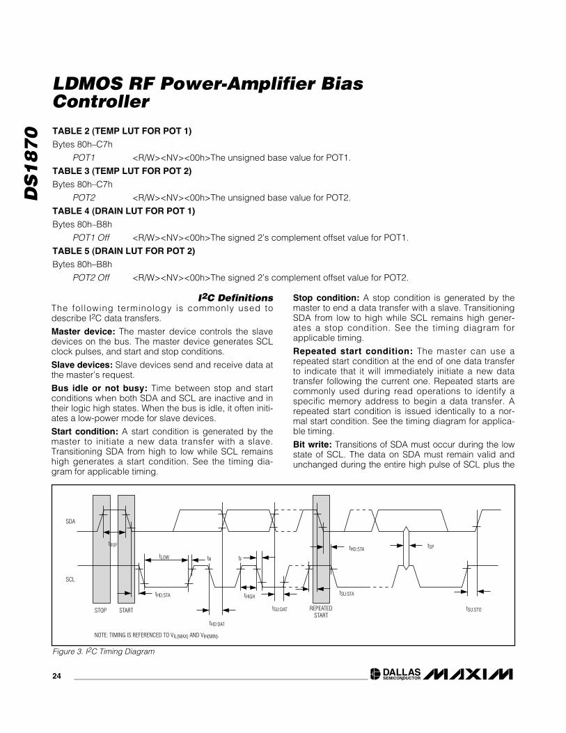
I2C DefinitionsThe following terminology is commonly used todescribe I2C data transfers.
Master device: The master device controls the slavedevices on the bus. The master device generates SCLclock pulses, and start and stop conditions.
Slave devices: Slave devices send and receive data atthe master’s request.
Bus idle or not busy: Time between stop and startconditions when both SDA and SCL are inactive and intheir logic high states. When the bus is idle, it often initi-ates a low-power mode for slave devices.
Start condition: A start condition is generated by themaster to initiate a new data transfer with a slave.Transitioning SDA from high to low while SCL remainshigh generates a start condition. See the timing dia-gram for applicable timing.
Stop condition: A stop condition is generated by themaster to end a data transfer with a slave. TransitioningSDA from low to high while SCL remains high gener-ates a stop condition. See the timing diagram forapplicable timing.
Repeated start condition: The master can use arepeated start condition at the end of one data transferto indicate that it will immediately initiate a new datatransfer following the current one. Repeated starts arecommonly used during read operations to identify aspecific memory address to begin a data transfer. Arepeated start condition is issued identically to a nor-mal start condition. See the timing diagram for applica-ble timing.
Bit write: Transitions of SDA must occur during the lowstate of SCL. The data on SDA must remain valid andunchanged during the entire high pulse of SCL plus the
SDA
SCL
tHD:STA
tLOW
tHIGH
tR tF
tBUF
tHD:DAT
tSU:DAT REPEATEDSTART
tSU:STA
tHD:STA
tSU:STO
tSP
STOP
NOTE: TIMING IS REFERENCED TO VIL(MAX) AND VIH(MIN).
START
Figure 3. I2C Timing Diagram
TABLE 2 (TEMP LUT FOR POT 1)
Bytes 80h–C7h
POT1 <R/W><NV><00h>The unsigned base value for POT1.
TABLE 3 (TEMP LUT FOR POT 2)
Bytes 80h–C7h
POT2 <R/W><NV><00h>The unsigned base value for POT2.
TABLE 4 (DRAIN LUT FOR POT 1)
Bytes 80h–B8h
POT1 Off <R/W><NV><00h>The signed 2’s complement offset value for POT1.
TABLE 5 (DRAIN LUT FOR POT 2)
Bytes 80h–B8h
POT2 Off <R/W><NV><00h>The signed 2’s complement offset value for POT2.
DS
18
70
LDMOS RF Power-Amplifier Bias Controller
____________________________________________________________________ 25
setup and hold time requirements (Figure 3). Data isshifted into the device during the rising edge of the SCL.
Bit read: At the end a write operation, the master mustrelease the SDA bus line for the proper amount of setuptime (Figure 3) before the next rising edge of SCL dur-ing a bit read. The device shifts out each bit of data onSDA at the falling edge of the previous SCL pulse andthe data bit is valid at the rising edge of the currentSCL pulse. Remember that the master generates allSCL clock pulses, including when it is reading bits fromthe slave.
Acknowledgement (ACK and NACK): An acknowl-edgement (ACK) or not acknowledge (NACK) is alwaysthe 9th bit transmitted during a byte transfer. Thedevice receiving data (the master during a read or theslave during a write operation) performs an ACK bytransmitting a zero during the 9th bit. A device per-forms a NACK by transmitting a one during the 9th bit.Timing (Figure 3) for the ACK and NACK is identical toall other bit writes. An ACK is the acknowledgment thatthe device is properly receiving data. A NACK is usedto terminate a read sequence or as an indication thatthe device is not receiving data.
Byte write: A byte write consists of 8 bits of informationtransferred from the master to the slave (most signifi-cant bit first) plus a 1-bit acknowledgement from theslave to the master. The 8 bits transmitted by the mas-ter are done according to the bit write definition and theacknowledgement is read using the bit read definition.
Byte read: A byte read is an 8-bit information transferfrom the slave to the master plus a 1-bit ACK or NACKfrom the master to the slave. The 8 bits of informationthat are transferred (most significant bit first) from theslave to the master are read by the master using the bitread definition above, and the master transmits an ACKusing the bit write definition to receive additional databytes. The master must NACK the last byte read to ter-minated communication so the slave will return controlof SDA to the master.
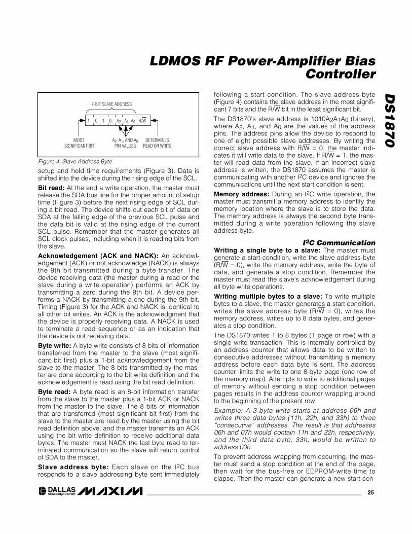
Slave address byte: Each slave on the I2C busresponds to a slave addressing byte sent immediately
following a start condition. The slave address byte(Figure 4) contains the slave address in the most signifi-cant 7 bits and the R/W bit in the least significant bit.
The DS1870’s slave address is 1010A2A1A0 (binary),where A2, A1, and A0 are the values of the addresspins. The address pins allow the device to respond toone of eight possible slave addresses. By writing thecorrect slave address with R/W = 0, the master indi-cates it will write data to the slave. If R/W = 1, the mas-ter will read data from the slave. If an incorrect slaveaddress is written, the DS1870 assumes the master iscommunicating with another I2C device and ignores thecommunications until the next start condition is sent.
Memory address: During an I2C write operation, themaster must transmit a memory address to identify thememory location where the slave is to store the data.The memory address is always the second byte trans-mitted during a write operation following the slaveaddress byte.
I2C CommunicationWriting a single byte to a slave: The master mustgenerate a start condition, write the slave address byte(R/W = 0), write the memory address, write the byte ofdata, and generate a stop condition. Remember themaster must read the slave’s acknowledgement duringall byte write operations.
Writing multiple bytes to a slave: To write multiplebytes to a slave, the master generates a start condition,writes the slave address byte (R/W = 0), writes thememory address, writes up to 8 data bytes, and gener-ates a stop condition.
The DS1870 writes 1 to 8 bytes (1 page or row) with asingle write transaction. This is internally controlled byan address counter that allows data to be written toconsecutive addresses without transmitting a memoryaddress before each data byte is sent. The addresscounter limits the write to one 8-byte page (one row ofthe memory map). Attempts to write to additional pagesof memory without sending a stop condition betweenpages results in the address counter wrapping aroundto the beginning of the present row.
Example: A 3-byte write starts at address 06h andwrites three data bytes (11h, 22h, and 33h) to three“consecutive” addresses. The result is that addresses06h and 07h would contain 11h and 22h, respectively,and the third data byte, 33h, would be written toaddress 00h.To prevent address wrapping from occurring, the mas-ter must send a stop condition at the end of the page,then wait for the bus-free or EEPROM-write time toelapse. Then the master can generate a new start con-
1 0 1 0 A2 A1 A0
7-BIT SLAVE ADDRESS
MOST SIGNIFICANT BIT
DETERMINESREAD OR WRITE
A2, A1, AND A0PIN VALUES
R/W
Figure 4. Slave Address Byte

DS
18
70
LDMOS RF Power-Amplifier Bias Controller
26 ____________________________________________________________________
dition, and write the slave address byte (R/W = 0) andthe first memory address of the next memory rowbefore continuing to write data.
Acknowledge polling: Any time an EEPROM page iswritten, the DS1870 requires the EEPROM write time(tW) after the stop condition to write the contents of thepage to EEPROM. During the EEPROM write time, theDS1870 wil l not acknowledge its slave addressbecause it is busy. It is possible to take advantage ofthat phenomenon by repeatedly addressing theDS1870, which allows the next page to be written assoon as the DS1870 is ready to receive the data. Thealternative to acknowledge polling is to wait for maxi-mum period of tW to elapse before attempting to writeagain to the DS1870.
EEPROM write cycles: When EEPROM writes occur,the DS1870 writes the whole EEPROM memory page,even if only a single byte on the page was modified.Writes that do not modify all 8 bytes on the page areallowed and do not corrupt the remaining bytes ofmemory on the same page. Because the whole page iswritten, bytes on the page that were not modified dur-ing the transaction are still subject to a write cycle. Thiscan result in a whole page being worn out over time bywriting a single byte repeatedly. Writing a page one
byte at a time wears the EEPROM out eight times fasterthan writing the entire page at once. The DS1870’sEEPROM write cycles are specified in the NonvolatileMemory Characteristics table. The specification shownis at the worst-case temperature. It can handle approxi-mately 10x that many writes at room temperature.Writing to SRAM-shadowed EEPROM memory with SEE= 1 does not count as an EEPROM write cycle whenevaluating the EEPROM’s estimated lifetime.
Reading a single byte from a slave: Unlike the writeoperation that uses the memory address byte to definewhere the data is to be written, the read operation occursat the present value of the memory address counter. Toread a single byte from the slave, the master generates astart condition, writes the slave address byte with R/W = 1, reads the data byte with a NACK to indicate theend of the transfer, and generates a stop condition.
Manipulating the address counter for reads: A dummywrite cycle can be used to force the address counter toa particular value. To do this, the master generates astart condition, writes the slave address byte (R/W = 0),writes the memory address where it desires to read, gen-erates a repeated start condition, writes the slaveaddress byte (R/W = 1), reads data with ACK or NACKas applicable, and generates a stop condition.
S
P
Sr
A
N
START
8 BITS ADDRESS OR DATAREPEATEDSTART
STOP
ACK
NOTACK
WHITE BOXES INDICATE THE MASTER ISCONTROLLING SDA
SHADED BOXES INDICATE THE SLAVE ISCONTROLLING SDA
WRITE A SINGLE BYTE
WRITE UP TO AN 8-BYTE PAGE WITH A SINGLE TRANSACTION
READ A SINGLE BYTE WITH A DUMMY WRITE CYCLE TO MOVE THE ADDRESS COUNTER
READ MULTIPLE BYTES WITH A DUMMY WRITE CYCLE TO MOVE THE ADDRESS COUNTER
COMMUNICATIONS KEY
S
X X X X X X X X
1 0 1 0 A0 0 A MEMORY ADDRESS A DATA A P
S 1 0 1 0 0 A MEMORY ADDRESS A DATA A DATA A P
S 1 0 1 0 0 A MEMORY ADDRESS A Sr 1 0 1 0 A0 1 A DATA N P
S 1 0 1 0 0 A MEMORY ADDRESS A Sr 1 0 1 0 1 A DATA A
DATA A DATA A DATA N P
NOTES:1) ALL BYTES ARE SENT MOST SIGNIFICANT BIT FIRST.2) THE FIRST BYTE SENT AFTER A START CONDITION IS ALWAYS THE SLAVE ADDRESS, FOLLOWED BY THE READ/WRITE BIT.
A1A2
A0A1A2
A0A1A2
A0A1A2
A1A2
A0A1A2
Figure 5. I2C Communications Examples

DS
18
70
LDMOS RF Power-Amplifier Bias Controller
____________________________________________________________________ 27
See Figure 5 for a read example using the repeatedstart condition to specify the starting memory location.
Reading multiple bytes from a slave: The read opera-tion can be used to read multiple bytes with a singletransfer. When reading bytes from the slave, the mastersimply ACKs the data byte if it desires to read anotherbyte before terminating the transaction. After the masterreads the last byte it NACKs to indicate the end of thetransfer and generates a stop condition. This can bedone with or without modifying the address counter’slocation before the read cycle. The DS1870’s addresscounter does not wrap on page boundaries during read
operations, but the counter will roll from its upper mostmemory address FFh to 00h if the last memory locationis read during the read transaction.
Application InformationPower-Supply Decoupling
To achieve best results, it is recommended that the powersupply is decoupled with a 0.01µF or a 0.1µF capacitor.Use high-quality, ceramic, surface-mount capacitors, andmount the capacitors as close as possible to the VCC andGND pins to minimize lead inductance.
SDA
SCL
A2
A1
A0
FAULT
VCC
GND
5V
5V REFERENCE
RPOT1RPOT2 RS2 RS1
49.9kΩ
4.22kΩ
RFPOWER
AMPRFIN RFOUT
W1
L 1W2
H COM
L 2
N.C. N.C.
N.C.
N.C.
4.7kΩ3 PLACES
28V
ID1
ID2
VD
FACTORY-CALIBRATED 13-BIT ADC(CUSTOMER ADJUSTABLE FULL-
SCALE AND OFFSET VALUES)
NOTES:1) IN THIS CONFIGURATION, THE VOLTAGE RANGE OF W1 AND W2 IS 3V-5V. THIS RANGE CAN BE EXTENDED USING EXTERNAL RESISTORS.2) ONE MAX6156B CAN BE USED WITH MULTIPLE DS1870s.
DS1870
MAX6165B
Typical Operating Circuit

DS
18
70
LDMOS RF Power-Amplifier Bias Controller
Maxim cannot assume responsibility for use of any circuitry other than circuitry entirely embodied in a Maxim product. No circuit patent licenses areimplied. Maxim reserves the right to change the circuitry and specifications without notice at any time.
28 ____________________Maxim Integrated Products, 120 San Gabriel Drive, Sunnyvale, CA 94086 408-737-7600
© 2006 Maxim Integrated Products is a registered trademark of Maxim Integrated Products, Inc.
is a registered trademark of Dallas Semiconductor Corporation.
SDA and SCL Pullup ResistorsSDA is an open-collector output on the DS1870 thatrequires a pullup resistor to realize high logic levels. Amaster using either an open-collector output with apullup resistor or a push-pull output driver can be usedfor SCL. Pullup resistor values should be chosen toensure that the rise and fall times listed in the AC elec-trical characteristics are within specification.
Advanced ApplicationA circuit showing the implementaion of current sensingusing the DS1870 is shown under AdvancedApplication with Current Sense.
SDA
SCL
A2
A1
A0
FAULT
VCC
GND
5V
5V REFERENCE
RPOT1
49.9k(1%)
LOWPASS
FILTER
RPOT2 RS2 RS1
4.22k(1%)
VD
ID1
ID2
RFPOWER
AMPRFIN RFOUT
W1
L 1W2
H COM
L 2
N.C. N.C.
4.7kΩ3 PLACES
NOTES:1) IN THIS CONFIGURATION, THE VOLTAGE RANGE OF W1 AND W2 IS 3V-5V. THIS RANGE CAN BE EXTENDED USING EXTERNAL RESISTORS.2) ONE MAX6156B CAN BE USED WITH MULTIPLE DS1870s.
DS1870
MAX6165B
MAX4080
LOWPASS
FILTERMAX4080
28V
Advanced Application with Current Sense
Chip InformationTRANSISTOR COUNT: 52,353
SUBSTRATE CONNECTED TO GROUND
Package InformationFor the latest package outline information, go towww.maxim-ic.com/DallasPackInfo.