Embed Size (px)
Citation preview

User's GuideSLVUAK8–November 2015
Evaluation Module for the TPS65235 LNB VoltageRegulator With I2C Interface for DiSEqC1.x Application
This document presents the information required to operate the TPS65235 as well as the supportdocumentation including schematic, layout, hardware setup, software application, key waveforms, and billof materials.
Contents1 Background ................................................................................................................... 22 Schematic..................................................................................................................... 23 Board Layout ................................................................................................................. 34 Bench Test Setup Conditions .............................................................................................. 55 Installing the Software....................................................................................................... 86 Software Operation .......................................................................................................... 87 Test Procedure Example .................................................................................................. 118 Bill Of Materials............................................................................................................. 12
List of Figures
1 TPS65235 EVM Schematic ................................................................................................ 22 Component Placement (Top Layer) ....................................................................................... 33 Board Layout (Top Layer) .................................................................................................. 44 Board Layout (Bottom Layer) .............................................................................................. 45 Headers Description and Jumper Placement ............................................................................ 56 USB Interface Adapter Quick Connection Diagram ..................................................................... 77 GUI Interface Home Page .................................................................................................. 88 GUI Bit Register Map Page ................................................................................................ 99 GUI Main Control Panel ................................................................................................... 1010 EXTM has 22-kHz External Tone Input ................................................................................. 1111 EXTM has Envelope Input for Tone Output Control ................................................................... 11
List of Tables
1 Input/Output Connection .................................................................................................... 62 Jumpers and Switches ...................................................................................................... 63 VLNB Output Control Without I2C Interface Connection................................................................ 64 I2C Address Selection...................................................................................................... 105 TPS65235EVM Bill Of Materials ......................................................................................... 12
Microsoft, Windows, Internet Explorer are registered trademarks of Microsoft Corporation.VERISIGN is a registered trademark of Verisign, Inc..
1SLVUAK8–November 2015 Evaluation Module for the TPS65235 LNB Voltage Regulator With I2CInterface for DiSEqC1.x ApplicationSubmit Documentation Feedback
Copyright © 2015, Texas Instruments Incorporated

GND
GND
GND
V3V
100kR7VIN
GND
GND
10k
R4
GND
GND
D1L1
10uH
100uFC4
DNP10uFC1
0.01 FμC7
1 FμC3
100kR2
10k
R3
EXTM
VCTRL
LX1
VIN2
VCC3
AGND4
TCAP5
ISET6
EN7
FAULT8
ADDR9
VCTRL10
SDA11
SCL12
EXTM13
DOUT14
DIN15
VLNB16
VCP17
BOOST18
GDR19
PGND20
EP21
U1
TPS65235RUKR
1
2
3
J4
1
2
3
J7
1 2
3 4
5 6
J6
1
2
3
J5
TP6
1 2
3 4
5 6
7 8
9 10
P1
0.022 FμC5
1 FμC6
110kR1
1 FμC2
TP3
GND
J2
GNDD0
DNP
VCC
VC
C
SCL
SDA
100kR6
33.0kR5
VCC
GND
BOOST
VCC
VCTRL
0.1 Fμ
C10
GND
D30.1 FμC11
D2DNP
GNDVOUT
FAULT VCC
GND
EXTM
SCLSDAADDREN
VIN
VCC
ISET
TCAP
TP1
LX
VCP
VOUT
J1
ADDR
EN
GND GND
TP5
TP7
22uFC9
GND
1 2 3
J3
22uFC8
TP4
GND
TP2
Background www.ti.com
1 BackgroundThe TPS65235 is designed to provide 13-V/18-V output voltage for a satellite receiver, with an operationalrange of 4.5 to 16 V.
The TPS65235 features I2C-controlled output voltage from 11 V to 20 V with 16 options; output currentlimit with ±10% accuracy is set with the ISET pin connecting different resistors. The maximum outputcurrent limit is up to 1 A.
The TPS65235 can also run without I2C. In non-I2C mode, the SCL pin and VCTRL pin are used to control13-V/18-V output, these two pins can be controlled by GPIO from the processor. A dedicated enable pin,EN, is available to turn the LNB output on and off.
The evaluation module is designed to provide access to the features of the TPS65235 for DiSEqC1.xapplication. Some modifications can be made to this module to test performance at different input andoutput voltages, current and switching frequency. Please contact TI Field Applications Group for advice onthese matters.
2 SchematicFigure 1 illustrates the TPS65235 EVM schematic.
Figure 1. TPS65235 EVM Schematic
In the TPS65235 application, the recommended ceramic capacitors rated are at least X7R/X5R, 35-Vrating and 1206 size for achieving lower LNB output ripple. For this EVM, two 22-µF, 35-V capacitors, C8and C9, are put at the output of the boost converter. If lower cost is demanded, a 100-µF electrolytic (lowESR) and a 10-µF/35-V ceramic capacitor also works well.
2 SLVUAK8–November 2015Evaluation Module for the TPS65235 LNB Voltage Regulator With I2CInterface for DiSEqC1.x Application Submit Documentation Feedback
Copyright © 2015, Texas Instruments Incorporated

www.ti.com Board Layout
3 Board LayoutFigure 2 shows the component placement on the EVM. Figure 3 and Figure 4 illustrate the top and bottomlayers, respectively.
Figure 2. Component Placement (Top Layer)
3SLVUAK8–November 2015 Evaluation Module for the TPS65235 LNB Voltage Regulator With I2CInterface for DiSEqC1.x ApplicationSubmit Documentation Feedback
Copyright © 2015, Texas Instruments Incorporated

Board Layout www.ti.com
Figure 3. Board Layout (Top Layer)
Figure 4. Board Layout (Bottom Layer)
4 SLVUAK8–November 2015Evaluation Module for the TPS65235 LNB Voltage Regulator With I2CInterface for DiSEqC1.x Application Submit Documentation Feedback
Copyright © 2015, Texas Instruments Incorporated

Test Point A
J2 VIN
J1 VOUT
J4
EXTM Control
J5
VCTRL Control
J3
SCL/I C Power2
P1
I C Interface to PC2
J6
ADDR Control
J7
EN Control
www.ti.com Bench Test Setup Conditions
4 Bench Test Setup Conditions
4.1 Headers Description and Jumper PlacementFigure 5 shows the header descriptions and jumper placement.
Figure 5. Headers Description and Jumper Placement
Test points:A: LX for Boost
Notes:• At non-I2C mode, P1 should be floating, J5 and J3 are used to set the output, refer to Table 3.• At I2C mode, P1 is connected to the PC through the USB-TO-GPIO box, which makes the SCL signal
to H. J5 can be used to set the default output when powered on, refer to Table 3.• P1 and J3 cannot be connected at the same time.
5SLVUAK8–November 2015 Evaluation Module for the TPS65235 LNB Voltage Regulator With I2CInterface for DiSEqC1.x ApplicationSubmit Documentation Feedback
Copyright © 2015, Texas Instruments Incorporated

Bench Test Setup Conditions www.ti.com
Table 1 lists the I/O connections and Table 2 lists the EVM jumpers and switches.
Table 1. Input/Output Connection
# Function DescriptionJ1 VOUT Connector VLNB outputJ2 VIN Connector Apply power supply through this connector
Table 2. Jumpers and Switches
# Function Placement CommentJ3 Output voltage control If the IC is not controlled by I2C, the VCTRL pin and SCL pin are
(SCL) combined to control the VLNB output voltage. Refer to Table 3 fordetails.spaceJumper J3-2 and J3-1 makes SCL to VCC connection and givesVLNB with output 14.6 V or 19.4 VspaceJumper J3-2 and J3-3 makes SCL to GND connection and givesVLNB with output 13.4 V or 18.2 V
I2C Power If the IC is controlled by I2C, this is used to provide the I2C power On-board VCC is 6.3 Vwhich is connected to the SCL and SDA through pull-up resistorsspaceLeaving non jumpers connected sets the power to be 3.3 V fromthe I2C interface adaptorspaceShorting the J3-1 and J3-2 with a jumper sets the power to beVCC
J4 Tone control (EXTM) Toggle the EXTM signal (J4-2 to J4-3 and then J4-2 to J4-1), theinternal tone signal is superimposed at the VLNB output VOUTspaceEXTM to GND (J4-2 to J4-3), no internal tone signal issuperimposed at VOUT
J5 Output voltage control If the IC is not controlled by I2C, the VCTRL pin and SCL pin are(VCTRL) combined to control the VLNB output voltage. Refer to Table 3 for
details.spaceJumper J5-2 and J5-1 makes VCTRL to VCC connection andgives VLNB with an output of 18.2 V or 19.4 VspaceJumper J5-2 and J5-3 makes VCTRL to VCC connection andgives VLNB with an output of 13.4 V or 14.6 V
J6 I2C address set (ADDR) This pin is the I2C address set pin; tie to VCC sets I2C address With 3 V- VCC - 0.8 V willwith 0x08H; floating, sets I2C address with 0x09H; tie to GND sets set the I2C address 0x11H;I2C address with 0x10H; resistor divider R9A and R9B makeADDR pin at the voltage to set the I2C address with 0x11H. Referto Table 4 for details.
J7 VLNB output enable Connect jumper EN to GND to disable the VLNB output ( shorts(EN) J7-2 to J7-3), connect EN to VIN through a 100-kΩ resistor to
enable the VLNB output (short J7-2 to J7-1)spaceLeaving open enables VLNB output too.
Table 3. VLNB Output Control Without I2C InterfaceConnection
EN SCL VCRTL VLNBH H H 19.4 VH H L 14.6 VH L H 18.2 VH L L 13.4 VL X X 0 V
6 SLVUAK8–November 2015Evaluation Module for the TPS65235 LNB Voltage Regulator With I2CInterface for DiSEqC1.x Application Submit Documentation Feedback
Copyright © 2015, Texas Instruments Incorporated
www.ti.com Bench Test Setup Conditions
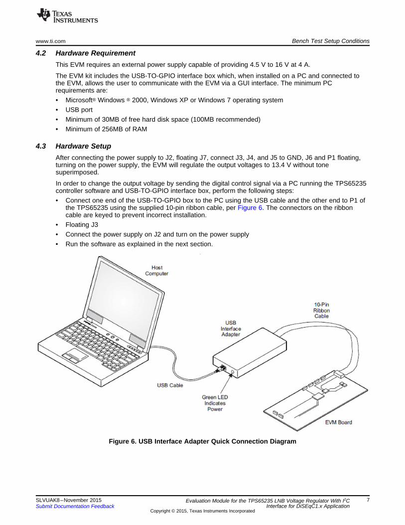
4.2 Hardware RequirementThis EVM requires an external power supply capable of providing 4.5 V to 16 V at 4 A.
The EVM kit includes the USB-TO-GPIO interface box which, when installed on a PC and connected tothe EVM, allows the user to communicate with the EVM via a GUI interface. The minimum PCrequirements are:• Microsoft® Windows ® 2000, Windows XP or Windows 7 operating system• USB port• Minimum of 30MB of free hard disk space (100MB recommended)• Minimum of 256MB of RAM
4.3 Hardware SetupAfter connecting the power supply to J2, floating J7, connect J3, J4, and J5 to GND, J6 and P1 floating,turning on the power supply, the EVM will regulate the output voltages to 13.4 V without tonesuperimposed.
In order to change the output voltage by sending the digital control signal via a PC running the TPS65235controller software and USB-TO-GPIO interface box, perform the following steps:• Connect one end of the USB-TO-GPIO box to the PC using the USB cable and the other end to P1 of
the TPS65235 using the supplied 10-pin ribbon cable, per Figure 6. The connectors on the ribboncable are keyed to prevent incorrect installation.
• Floating J3• Connect the power supply on J2 and turn on the power supply• Run the software as explained in the next section.
Figure 6. USB Interface Adapter Quick Connection Diagram
7SLVUAK8–November 2015 Evaluation Module for the TPS65235 LNB Voltage Regulator With I2CInterface for DiSEqC1.x ApplicationSubmit Documentation Feedback
Copyright © 2015, Texas Instruments Incorporated

Basic InformationAbout TPS65235
Status for USBAdapter Connection
Main ControlPanel
Register Map
Installing the Software www.ti.com
5 Installing the SoftwareIf installing from the TI Web site, visit the www.ti.com/product/TPS65235/toolssoftware URL.
NOTE: This installation page is best viewed with Microsoft Internet Explorer® browser (it may notwork correctly with other browsers).
1. Click on the install button; your PC should display a security warning and ask if you want to install thisapplication. Select Install to proceed.
2. To run the software after installation, either use the desktop icon, which is created by the installer if theuser agrees to creating a desktop icon, or go to Start → All programs → Texas Instruments →TPS65235.At start-up, the software first checks the firmware version of the USB-to-GPIO adapter box. If anincorrect firmware version is installed, the software automatically searches on the Internet (ifconnected) for updates. If a new update is available, the software notifies the user of the update, anddownloads and installs the software. Note that after the firmware is updated, the user must disconnectand then reconnect the USB cable between the adapter and PC, as instructed during the installprocess. The host PC software also automatically searches on the Internet (if connected) for updates.If a new update is available, the software notifies the user of the update and downloads and installs it.During future use of the software, you are prompted to install a new version if one becomes availableon the Web.
NOTE: VERISIGN® Code Signing is used to prevent any malicious code from changing thisapplication. If at any time in the future the binaries are modified, the code will no longerattempt to run.
6 Software OperationThis section provides descriptions of the EVM software.
The supplied software is used to communicate with the TPS65235EVM. Click on the icon on the hostcomputer to start the software. The software first displays the home page for the user interface. Entrancesare available for the expert user or beginner.
Figure 7. GUI Interface Home Page
8 SLVUAK8–November 2015Evaluation Module for the TPS65235 LNB Voltage Regulator With I2CInterface for DiSEqC1.x Application Submit Documentation Feedback
Copyright © 2015, Texas Instruments Incorporated

www.ti.com Software Operation
Click on the “B” button, the “Basic information about TPS65235” page comes up which lists the featuresand application information for TPS65235. Follow the steps, the GUI guides the beginner to setup theEVM and GUI step by step to do the basic check for the EVM.
6.1 Register Map PageClick the “E” button, the Register Map interface (Figure 8) displays.
Figure 8. GUI Bit Register Map Page
Single click on the register, the right “FIELD VIEW” comes up showing the detail setting of each bit.
Double clicking on the bit can change the it to “0” or “1”.
Single click on the “?” for the register, the detail description page for this register displays.
For the “Write Registers” option, when the “Immediate” button is selected, any change is sent to the EVMimmediately; otherwise, “Write Registers” button for each register must be clicked to send the controlsignal.
Register values can be read back from the EVM by clicking “Read Register” for each register or “Load AllRegisters” or set the “Auto Read” choice.
The Status for USB Adapter Connection only shows the status for the adapter, not the EVM board. Thecustomer can click the Write Registers on the Register Map page to verify the board communication.
6.2 Basic SettingsClicking the main control panel displays the “Basic Settings” interface. This interface provides a simplemethod for setting registers. Clicking the “Auto Read” button allows the register status to be monitoredautomatically.
9SLVUAK8–November 2015 Evaluation Module for the TPS65235 LNB Voltage Regulator With I2CInterface for DiSEqC1.x ApplicationSubmit Documentation Feedback
Copyright © 2015, Texas Instruments Incorporated

Control Register 1 Setup Status RegisterStatus Register Auto Read Choice
Control Register 2 Setup
Software Operation www.ti.com
Figure 9. GUI Main Control Panel
Figure 7 to Figure 9 show the control GUI interface. There are three 8-bit registers embedded in theTPS65235; two to control the output voltage characteristics, and one for status feedback. Make changesby selecting and checking the components on the Basic Settings page in the GUI. Changes are also madeby directly clicking the bits of each register on the Register Map page. Set the I2C address with J6 tocontrol the ADDR pin, refer to Table 2 and Table 4.
Table 4. I2C Address Selection
ADDR Pin I2C AddressConnect to VCC 0x08HFloating 0x09HConnected to GND 0x10HResistor divider to make ADDR pin voltage in 3 V ~ VCC-0.8 V 0x11H
10 SLVUAK8–November 2015Evaluation Module for the TPS65235 LNB Voltage Regulator With I2CInterface for DiSEqC1.x Application Submit Documentation Feedback
Copyright © 2015, Texas Instruments Incorporated

www.ti.com Test Procedure Example
7 Test Procedure Example
7.1 Voltage Output CheckUse the following voltage output checks while testing the EVM:1. Connect I2C adapter to P12. Floating J3, J6, and J7, J4 to GND, J5 to GND3. Apply 12 V to J24. Apply loads or non load to the output connector J1, check the output5. Set the control register 0x00H and 0x01H to the expected output value and then check the output6. Monitor the status register 0x02H for the IC status
7.2 Tone OutputUse the following tone output checks while testing the EVM:1. Connect I2C adaptor to P12. Floating J3, J6, and J7, J5 to GND3. Apply 12 V to J24. Toggle the EXTM (J4) from low to high, check the tone output at VOUT5. Apply loads or non-load to the output connector J1, check the output
Figure 10. EXTM has 22-kHz External Tone Input
Figure 11. EXTM has Envelope Input for Tone Output Control
11SLVUAK8–November 2015 Evaluation Module for the TPS65235 LNB Voltage Regulator With I2CInterface for DiSEqC1.x ApplicationSubmit Documentation Feedback
Copyright © 2015, Texas Instruments Incorporated

Bill Of Materials www.ti.com
8 Bill Of MaterialsTable 5 lists the EVM BOM.
Table 5. TPS65235EVM Bill Of Materials
Designator Description Manufacturer Part Number QtyPCB1 Printed Circuit Board Any PWR747 1C1 CAP, CERM, 10 µF, 25 V, +/- 10%, X5R, 1206 Murata GRM31CR61E106KA12L 1C2, C3, C6 CAP, CERM, 1 μF, 25 V, +/- 10%, X5R, 0603 Murata GRM188R61E105KA12D 3C5 CAP, CERM, 0.022 μF, 50 V, +/- 10%, X7R, Murata GRM188R71H223KA01D 1
0603C7 CAP, CERM, 0.01 μF, 50 V, +/- 10%, X7R, Murata GRM188R71H103KA01D 1
0603C8, C9 CAP, CERM, 22 µF, 35 V, +/- 20%, X5R, TDK C3216X5R1V226M 2
1206_190C10 CAP, CERM, 0.1 μF, 16 V, +/- 5%, X7R, 0603 AVX 0603YC104JAT2A 1C11 CAP, CERM, 0.1 μF, 50 V, +/- 10%, X7R, Murata GRM188R71H104KA93D 1
0603D1 Diode, Schottky, 40 V, 3 A, SMA Diodes Inc. B340A-13-F 1D3 Diode, Schottky, 40 V, 2 A, SMA Diodes Inc. B240A-13-F 1H1, H2, H3, H4 Bumpon, Hemisphere, 0.44 X 0.20, Clear 3M SJ-5303 (CLEAR) 4J1, J2 Terminal Block, 6A, 3.5mm Pitch, 2-Pos, TH On-Shore Technology ED555/2DS 2J3, J4, J5, J7 Header, 100mil, 3x1, Gold, TH Samtec TSW-103-07-G-S 4J6 Header, 100mil, 3x2, Gold, TH Samtec TSW-103-07-G-D 1L1 Inductor, Shielded, Ferrite, 10 μH, 4 A, 0.0312 TDK CLF10040T-100M 1
ohm, SMDP1 Header (shrouded), 100mil, 5x2, Gold, TH Omron Electronic XG4C-1031 1
ComponentsR1 RES, 110 k, 1%, 0.1 W, 0603 Vishay-Dale CRCW0603110KFKEA 1R2, R6, R7 RES, 100 k, 1%, 0.1 W, 0603 Vishay-Dale CRCW0603100KFKEA 3R3, R4 RES, 10 k, 5%, 0.1 W, 0603 Vishay-Dale CRCW060310K0JNEA 2R5 RES, 33.0 k, 1%, 0.1 W, 0603 Vishay-Dale CRCW060333K0FKEA 1SH-J1 Shunt, 100mil, Gold plated, Black 3M 969102-0000-DA 1TP1, TP2, TP3 Test Point, Multipurpose, Red, TH Keystone 5010 3TP4, TP5, TP6, Test Point, Multipurpose, White, TH Keystone 5012 4TP7U1 LNB VOLTAGE REGULATOR WITH I2C Texas Instruments TPS65235RUKR 1
INTERFACE
12 SLVUAK8–November 2015Evaluation Module for the TPS65235 LNB Voltage Regulator With I2CInterface for DiSEqC1.x Application Submit Documentation Feedback
Copyright © 2015, Texas Instruments Incorporated

STANDARD TERMS AND CONDITIONS FOR EVALUATION MODULES1. Delivery: TI delivers TI evaluation boards, kits, or modules, including any accompanying demonstration software, components, or
documentation (collectively, an “EVM” or “EVMs”) to the User (“User”) in accordance with the terms and conditions set forth herein.Acceptance of the EVM is expressly subject to the following terms and conditions.1.1 EVMs are intended solely for product or software developers for use in a research and development setting to facilitate feasibility
evaluation, experimentation, or scientific analysis of TI semiconductors products. EVMs have no direct function and are notfinished products. EVMs shall not be directly or indirectly assembled as a part or subassembly in any finished product. Forclarification, any software or software tools provided with the EVM (“Software”) shall not be subject to the terms and conditionsset forth herein but rather shall be subject to the applicable terms and conditions that accompany such Software
1.2 EVMs are not intended for consumer or household use. EVMs may not be sold, sublicensed, leased, rented, loaned, assigned,or otherwise distributed for commercial purposes by Users, in whole or in part, or used in any finished product or productionsystem.
2 Limited Warranty and Related Remedies/Disclaimers:2.1 These terms and conditions do not apply to Software. The warranty, if any, for Software is covered in the applicable Software
License Agreement.2.2 TI warrants that the TI EVM will conform to TI's published specifications for ninety (90) days after the date TI delivers such EVM
to User. Notwithstanding the foregoing, TI shall not be liable for any defects that are caused by neglect, misuse or mistreatmentby an entity other than TI, including improper installation or testing, or for any EVMs that have been altered or modified in anyway by an entity other than TI. Moreover, TI shall not be liable for any defects that result from User's design, specifications orinstructions for such EVMs. Testing and other quality control techniques are used to the extent TI deems necessary or asmandated by government requirements. TI does not test all parameters of each EVM.
2.3 If any EVM fails to conform to the warranty set forth above, TI's sole liability shall be at its option to repair or replace such EVM,or credit User's account for such EVM. TI's liability under this warranty shall be limited to EVMs that are returned during thewarranty period to the address designated by TI and that are determined by TI not to conform to such warranty. If TI elects torepair or replace such EVM, TI shall have a reasonable time to repair such EVM or provide replacements. Repaired EVMs shallbe warranted for the remainder of the original warranty period. Replaced EVMs shall be warranted for a new full ninety (90) daywarranty period.
3 Regulatory Notices:3.1 United States
3.1.1 Notice applicable to EVMs not FCC-Approved:This kit is designed to allow product developers to evaluate electronic components, circuitry, or software associated with the kitto determine whether to incorporate such items in a finished product and software developers to write software applications foruse with the end product. This kit is not a finished product and when assembled may not be resold or otherwise marketed unlessall required FCC equipment authorizations are first obtained. Operation is subject to the condition that this product not causeharmful interference to licensed radio stations and that this product accept harmful interference. Unless the assembled kit isdesigned to operate under part 15, part 18 or part 95 of this chapter, the operator of the kit must operate under the authority ofan FCC license holder or must secure an experimental authorization under part 5 of this chapter.3.1.2 For EVMs annotated as FCC – FEDERAL COMMUNICATIONS COMMISSION Part 15 Compliant:
CAUTIONThis device complies with part 15 of the FCC Rules. Operation is subject to the following two conditions: (1) This device may notcause harmful interference, and (2) this device must accept any interference received, including interference that may causeundesired operation.Changes or modifications not expressly approved by the party responsible for compliance could void the user's authority tooperate the equipment.
FCC Interference Statement for Class A EVM devicesNOTE: This equipment has been tested and found to comply with the limits for a Class A digital device, pursuant to part 15 ofthe FCC Rules. These limits are designed to provide reasonable protection against harmful interference when the equipment isoperated in a commercial environment. This equipment generates, uses, and can radiate radio frequency energy and, if notinstalled and used in accordance with the instruction manual, may cause harmful interference to radio communications.Operation of this equipment in a residential area is likely to cause harmful interference in which case the user will be required tocorrect the interference at his own expense.
SPACER
SPACER
SPACER
SPACER
SPACER
SPACER
SPACER
SPACER

FCC Interference Statement for Class B EVM devicesNOTE: This equipment has been tested and found to comply with the limits for a Class B digital device, pursuant to part 15 ofthe FCC Rules. These limits are designed to provide reasonable protection against harmful interference in a residentialinstallation. This equipment generates, uses and can radiate radio frequency energy and, if not installed and used in accordancewith the instructions, may cause harmful interference to radio communications. However, there is no guarantee that interferencewill not occur in a particular installation. If this equipment does cause harmful interference to radio or television reception, whichcan be determined by turning the equipment off and on, the user is encouraged to try to correct the interference by one or moreof the following measures:
• Reorient or relocate the receiving antenna.• Increase the separation between the equipment and receiver.• Connect the equipment into an outlet on a circuit different from that to which the receiver is connected.• Consult the dealer or an experienced radio/TV technician for help.
3.2 Canada3.2.1 For EVMs issued with an Industry Canada Certificate of Conformance to RSS-210
Concerning EVMs Including Radio Transmitters:This device complies with Industry Canada license-exempt RSS standard(s). Operation is subject to the following two conditions:(1) this device may not cause interference, and (2) this device must accept any interference, including interference that maycause undesired operation of the device.
Concernant les EVMs avec appareils radio:Le présent appareil est conforme aux CNR d'Industrie Canada applicables aux appareils radio exempts de licence. L'exploitationest autorisée aux deux conditions suivantes: (1) l'appareil ne doit pas produire de brouillage, et (2) l'utilisateur de l'appareil doitaccepter tout brouillage radioélectrique subi, même si le brouillage est susceptible d'en compromettre le fonctionnement.
Concerning EVMs Including Detachable Antennas:Under Industry Canada regulations, this radio transmitter may only operate using an antenna of a type and maximum (or lesser)gain approved for the transmitter by Industry Canada. To reduce potential radio interference to other users, the antenna typeand its gain should be so chosen that the equivalent isotropically radiated power (e.i.r.p.) is not more than that necessary forsuccessful communication. This radio transmitter has been approved by Industry Canada to operate with the antenna typeslisted in the user guide with the maximum permissible gain and required antenna impedance for each antenna type indicated.Antenna types not included in this list, having a gain greater than the maximum gain indicated for that type, are strictly prohibitedfor use with this device.
Concernant les EVMs avec antennes détachablesConformément à la réglementation d'Industrie Canada, le présent émetteur radio peut fonctionner avec une antenne d'un type etd'un gain maximal (ou inférieur) approuvé pour l'émetteur par Industrie Canada. Dans le but de réduire les risques de brouillageradioélectrique à l'intention des autres utilisateurs, il faut choisir le type d'antenne et son gain de sorte que la puissance isotroperayonnée équivalente (p.i.r.e.) ne dépasse pas l'intensité nécessaire à l'établissement d'une communication satisfaisante. Leprésent émetteur radio a été approuvé par Industrie Canada pour fonctionner avec les types d'antenne énumérés dans lemanuel d’usage et ayant un gain admissible maximal et l'impédance requise pour chaque type d'antenne. Les types d'antennenon inclus dans cette liste, ou dont le gain est supérieur au gain maximal indiqué, sont strictement interdits pour l'exploitation del'émetteur
3.3 Japan3.3.1 Notice for EVMs delivered in Japan: Please see http://www.tij.co.jp/lsds/ti_ja/general/eStore/notice_01.page 日本国内に
輸入される評価用キット、ボードについては、次のところをご覧ください。http://www.tij.co.jp/lsds/ti_ja/general/eStore/notice_01.page
3.3.2 Notice for Users of EVMs Considered “Radio Frequency Products” in Japan: EVMs entering Japan may not be certifiedby TI as conforming to Technical Regulations of Radio Law of Japan.
If User uses EVMs in Japan, not certified to Technical Regulations of Radio Law of Japan, User is required by Radio Law ofJapan to follow the instructions below with respect to EVMs:1. Use EVMs in a shielded room or any other test facility as defined in the notification #173 issued by Ministry of Internal
Affairs and Communications on March 28, 2006, based on Sub-section 1.1 of Article 6 of the Ministry’s Rule forEnforcement of Radio Law of Japan,
2. Use EVMs only after User obtains the license of Test Radio Station as provided in Radio Law of Japan with respect toEVMs, or
3. Use of EVMs only after User obtains the Technical Regulations Conformity Certification as provided in Radio Law of Japanwith respect to EVMs. Also, do not transfer EVMs, unless User gives the same notice above to the transferee. Please notethat if User does not follow the instructions above, User will be subject to penalties of Radio Law of Japan.
SPACER
SPACER
SPACER
SPACER
SPACER

【無線電波を送信する製品の開発キットをお使いになる際の注意事項】 開発キットの中には技術基準適合証明を受けていないものがあります。 技術適合証明を受けていないもののご使用に際しては、電波法遵守のため、以下のいずれかの措置を取っていただく必要がありますのでご注意ください。1. 電波法施行規則第6条第1項第1号に基づく平成18年3月28日総務省告示第173号で定められた電波暗室等の試験設備でご使用
いただく。2. 実験局の免許を取得後ご使用いただく。3. 技術基準適合証明を取得後ご使用いただく。
なお、本製品は、上記の「ご使用にあたっての注意」を譲渡先、移転先に通知しない限り、譲渡、移転できないものとします。上記を遵守頂けない場合は、電波法の罰則が適用される可能性があることをご留意ください。 日本テキサス・イ
ンスツルメンツ株式会社東京都新宿区西新宿6丁目24番1号西新宿三井ビル
3.3.3 Notice for EVMs for Power Line Communication: Please see http://www.tij.co.jp/lsds/ti_ja/general/eStore/notice_02.page電力線搬送波通信についての開発キットをお使いになる際の注意事項については、次のところをご覧ください。http://www.tij.co.jp/lsds/ti_ja/general/eStore/notice_02.page
SPACER4 EVM Use Restrictions and Warnings:
4.1 EVMS ARE NOT FOR USE IN FUNCTIONAL SAFETY AND/OR SAFETY CRITICAL EVALUATIONS, INCLUDING BUT NOTLIMITED TO EVALUATIONS OF LIFE SUPPORT APPLICATIONS.
4.2 User must read and apply the user guide and other available documentation provided by TI regarding the EVM prior to handlingor using the EVM, including without limitation any warning or restriction notices. The notices contain important safety informationrelated to, for example, temperatures and voltages.
4.3 Safety-Related Warnings and Restrictions:4.3.1 User shall operate the EVM within TI’s recommended specifications and environmental considerations stated in the user
guide, other available documentation provided by TI, and any other applicable requirements and employ reasonable andcustomary safeguards. Exceeding the specified performance ratings and specifications (including but not limited to inputand output voltage, current, power, and environmental ranges) for the EVM may cause personal injury or death, orproperty damage. If there are questions concerning performance ratings and specifications, User should contact a TIfield representative prior to connecting interface electronics including input power and intended loads. Any loads appliedoutside of the specified output range may also result in unintended and/or inaccurate operation and/or possiblepermanent damage to the EVM and/or interface electronics. Please consult the EVM user guide prior to connecting anyload to the EVM output. If there is uncertainty as to the load specification, please contact a TI field representative.During normal operation, even with the inputs and outputs kept within the specified allowable ranges, some circuitcomponents may have elevated case temperatures. These components include but are not limited to linear regulators,switching transistors, pass transistors, current sense resistors, and heat sinks, which can be identified using theinformation in the associated documentation. When working with the EVM, please be aware that the EVM may becomevery warm.
4.3.2 EVMs are intended solely for use by technically qualified, professional electronics experts who are familiar with thedangers and application risks associated with handling electrical mechanical components, systems, and subsystems.User assumes all responsibility and liability for proper and safe handling and use of the EVM by User or its employees,affiliates, contractors or designees. User assumes all responsibility and liability to ensure that any interfaces (electronicand/or mechanical) between the EVM and any human body are designed with suitable isolation and means to safelylimit accessible leakage currents to minimize the risk of electrical shock hazard. User assumes all responsibility andliability for any improper or unsafe handling or use of the EVM by User or its employees, affiliates, contractors ordesignees.
4.4 User assumes all responsibility and liability to determine whether the EVM is subject to any applicable international, federal,state, or local laws and regulations related to User’s handling and use of the EVM and, if applicable, User assumes allresponsibility and liability for compliance in all respects with such laws and regulations. User assumes all responsibility andliability for proper disposal and recycling of the EVM consistent with all applicable international, federal, state, and localrequirements.
5. Accuracy of Information: To the extent TI provides information on the availability and function of EVMs, TI attempts to be as accurateas possible. However, TI does not warrant the accuracy of EVM descriptions, EVM availability or other information on its websites asaccurate, complete, reliable, current, or error-free.
SPACER
SPACER
SPACER
SPACER
SPACER
SPACER

SPACER6. Disclaimers:
6.1 EXCEPT AS SET FORTH ABOVE, EVMS AND ANY WRITTEN DESIGN MATERIALS PROVIDED WITH THE EVM (AND THEDESIGN OF THE EVM ITSELF) ARE PROVIDED "AS IS" AND "WITH ALL FAULTS." TI DISCLAIMS ALL OTHERWARRANTIES, EXPRESS OR IMPLIED, REGARDING SUCH ITEMS, INCLUDING BUT NOT LIMITED TO ANY IMPLIEDWARRANTIES OF MERCHANTABILITY OR FITNESS FOR A PARTICULAR PURPOSE OR NON-INFRINGEMENT OF ANYTHIRD PARTY PATENTS, COPYRIGHTS, TRADE SECRETS OR OTHER INTELLECTUAL PROPERTY RIGHTS.
6.2 EXCEPT FOR THE LIMITED RIGHT TO USE THE EVM SET FORTH HEREIN, NOTHING IN THESE TERMS ANDCONDITIONS SHALL BE CONSTRUED AS GRANTING OR CONFERRING ANY RIGHTS BY LICENSE, PATENT, OR ANYOTHER INDUSTRIAL OR INTELLECTUAL PROPERTY RIGHT OF TI, ITS SUPPLIERS/LICENSORS OR ANY OTHER THIRDPARTY, TO USE THE EVM IN ANY FINISHED END-USER OR READY-TO-USE FINAL PRODUCT, OR FOR ANYINVENTION, DISCOVERY OR IMPROVEMENT MADE, CONCEIVED OR ACQUIRED PRIOR TO OR AFTER DELIVERY OFTHE EVM.
7. USER'S INDEMNITY OBLIGATIONS AND REPRESENTATIONS. USER WILL DEFEND, INDEMNIFY AND HOLD TI, ITSLICENSORS AND THEIR REPRESENTATIVES HARMLESS FROM AND AGAINST ANY AND ALL CLAIMS, DAMAGES, LOSSES,EXPENSES, COSTS AND LIABILITIES (COLLECTIVELY, "CLAIMS") ARISING OUT OF OR IN CONNECTION WITH ANYHANDLING OR USE OF THE EVM THAT IS NOT IN ACCORDANCE WITH THESE TERMS AND CONDITIONS. THIS OBLIGATIONSHALL APPLY WHETHER CLAIMS ARISE UNDER STATUTE, REGULATION, OR THE LAW OF TORT, CONTRACT OR ANYOTHER LEGAL THEORY, AND EVEN IF THE EVM FAILS TO PERFORM AS DESCRIBED OR EXPECTED.
8. Limitations on Damages and Liability:8.1 General Limitations. IN NO EVENT SHALL TI BE LIABLE FOR ANY SPECIAL, COLLATERAL, INDIRECT, PUNITIVE,
INCIDENTAL, CONSEQUENTIAL, OR EXEMPLARY DAMAGES IN CONNECTION WITH OR ARISING OUT OF THESETERMS ANDCONDITIONS OR THE USE OF THE EVMS PROVIDED HEREUNDER, REGARDLESS OF WHETHER TI HASBEEN ADVISED OF THE POSSIBILITY OF SUCH DAMAGES. EXCLUDED DAMAGES INCLUDE, BUT ARE NOT LIMITEDTO, COST OF REMOVAL OR REINSTALLATION, ANCILLARY COSTS TO THE PROCUREMENT OF SUBSTITUTE GOODSOR SERVICES, RETESTING, OUTSIDE COMPUTER TIME, LABOR COSTS, LOSS OF GOODWILL, LOSS OF PROFITS,LOSS OF SAVINGS, LOSS OF USE, LOSS OF DATA, OR BUSINESS INTERRUPTION. NO CLAIM, SUIT OR ACTION SHALLBE BROUGHT AGAINST TI MORE THAN ONE YEAR AFTER THE RELATED CAUSE OF ACTION HAS OCCURRED.
8.2 Specific Limitations. IN NO EVENT SHALL TI'S AGGREGATE LIABILITY FROM ANY WARRANTY OR OTHER OBLIGATIONARISING OUT OF OR IN CONNECTION WITH THESE TERMS AND CONDITIONS, OR ANY USE OF ANY TI EVMPROVIDED HEREUNDER, EXCEED THE TOTAL AMOUNT PAID TO TI FOR THE PARTICULAR UNITS SOLD UNDERTHESE TERMS AND CONDITIONS WITH RESPECT TO WHICH LOSSES OR DAMAGES ARE CLAIMED. THE EXISTENCEOF MORE THAN ONE CLAIM AGAINST THE PARTICULAR UNITS SOLD TO USER UNDER THESE TERMS ANDCONDITIONS SHALL NOT ENLARGE OR EXTEND THIS LIMIT.
9. Return Policy. Except as otherwise provided, TI does not offer any refunds, returns, or exchanges. Furthermore, no return of EVM(s)will be accepted if the package has been opened and no return of the EVM(s) will be accepted if they are damaged or otherwise not ina resalable condition. If User feels it has been incorrectly charged for the EVM(s) it ordered or that delivery violates the applicableorder, User should contact TI. All refunds will be made in full within thirty (30) working days from the return of the components(s),excluding any postage or packaging costs.
10. Governing Law: These terms and conditions shall be governed by and interpreted in accordance with the laws of the State of Texas,without reference to conflict-of-laws principles. User agrees that non-exclusive jurisdiction for any dispute arising out of or relating tothese terms and conditions lies within courts located in the State of Texas and consents to venue in Dallas County, Texas.Notwithstanding the foregoing, any judgment may be enforced in any United States or foreign court, and TI may seek injunctive reliefin any United States or foreign court.
Mailing Address: Texas Instruments, Post Office Box 655303, Dallas, Texas 75265Copyright © 2015, Texas Instruments Incorporated
spacer

IMPORTANT NOTICE
Texas Instruments Incorporated and its subsidiaries (TI) reserve the right to make corrections, enhancements, improvements and otherchanges to its semiconductor products and services per JESD46, latest issue, and to discontinue any product or service per JESD48, latestissue. Buyers should obtain the latest relevant information before placing orders and should verify that such information is current andcomplete. All semiconductor products (also referred to herein as “components”) are sold subject to TI’s terms and conditions of salesupplied at the time of order acknowledgment.TI warrants performance of its components to the specifications applicable at the time of sale, in accordance with the warranty in TI’s termsand conditions of sale of semiconductor products. Testing and other quality control techniques are used to the extent TI deems necessaryto support this warranty. Except where mandated by applicable law, testing of all parameters of each component is not necessarilyperformed.TI assumes no liability for applications assistance or the design of Buyers’ products. Buyers are responsible for their products andapplications using TI components. To minimize the risks associated with Buyers’ products and applications, Buyers should provideadequate design and operating safeguards.TI does not warrant or represent that any license, either express or implied, is granted under any patent right, copyright, mask work right, orother intellectual property right relating to any combination, machine, or process in which TI components or services are used. Informationpublished by TI regarding third-party products or services does not constitute a license to use such products or services or a warranty orendorsement thereof. Use of such information may require a license from a third party under the patents or other intellectual property of thethird party, or a license from TI under the patents or other intellectual property of TI.Reproduction of significant portions of TI information in TI data books or data sheets is permissible only if reproduction is without alterationand is accompanied by all associated warranties, conditions, limitations, and notices. TI is not responsible or liable for such altereddocumentation. Information of third parties may be subject to additional restrictions.Resale of TI components or services with statements different from or beyond the parameters stated by TI for that component or servicevoids all express and any implied warranties for the associated TI component or service and is an unfair and deceptive business practice.TI is not responsible or liable for any such statements.Buyer acknowledges and agrees that it is solely responsible for compliance with all legal, regulatory and safety-related requirementsconcerning its products, and any use of TI components in its applications, notwithstanding any applications-related information or supportthat may be provided by TI. Buyer represents and agrees that it has all the necessary expertise to create and implement safeguards whichanticipate dangerous consequences of failures, monitor failures and their consequences, lessen the likelihood of failures that might causeharm and take appropriate remedial actions. Buyer will fully indemnify TI and its representatives against any damages arising out of the useof any TI components in safety-critical applications.In some cases, TI components may be promoted specifically to facilitate safety-related applications. With such components, TI’s goal is tohelp enable customers to design and create their own end-product solutions that meet applicable functional safety standards andrequirements. Nonetheless, such components are subject to these terms.No TI components are authorized for use in FDA Class III (or similar life-critical medical equipment) unless authorized officers of the partieshave executed a special agreement specifically governing such use.Only those TI components which TI has specifically designated as military grade or “enhanced plastic” are designed and intended for use inmilitary/aerospace applications or environments. Buyer acknowledges and agrees that any military or aerospace use of TI componentswhich have not been so designated is solely at the Buyer's risk, and that Buyer is solely responsible for compliance with all legal andregulatory requirements in connection with such use.TI has specifically designated certain components as meeting ISO/TS16949 requirements, mainly for automotive use. In any case of use ofnon-designated products, TI will not be responsible for any failure to meet ISO/TS16949.
Products ApplicationsAudio www.ti.com/audio Automotive and Transportation www.ti.com/automotiveAmplifiers amplifier.ti.com Communications and Telecom www.ti.com/communicationsData Converters dataconverter.ti.com Computers and Peripherals www.ti.com/computersDLP® Products www.dlp.com Consumer Electronics www.ti.com/consumer-appsDSP dsp.ti.com Energy and Lighting www.ti.com/energyClocks and Timers www.ti.com/clocks Industrial www.ti.com/industrialInterface interface.ti.com Medical www.ti.com/medicalLogic logic.ti.com Security www.ti.com/securityPower Mgmt power.ti.com Space, Avionics and Defense www.ti.com/space-avionics-defenseMicrocontrollers microcontroller.ti.com Video and Imaging www.ti.com/videoRFID www.ti-rfid.comOMAP Applications Processors www.ti.com/omap TI E2E Community e2e.ti.comWireless Connectivity www.ti.com/wirelessconnectivity
Mailing Address: Texas Instruments, Post Office Box 655303, Dallas, Texas 75265Copyright © 2015, Texas Instruments Incorporated