Embed Size (px)
Citation preview
EVALUATION OF DIELECTRIC PROPERTIES OF POLYMER THIN-FILM MATERIALS FOR APPLICATION IN EMBEDDED CAPACITANCE
Jan Obrzut C. K. Chiang R. Popielarz R. Nozaki
Polymers Division 100 Bureau Drive, Gaithersburg, MD 20899-8541 USA September 2000
NISTIR 6537
2
EXECUTIVE BRIEF
Evaluation of Dielectric Properties of Polymer Thin-Film Materials
for Application in Embedded Capacitance
The relative dielectric constant of the embedded capacitance materials was measured in the frequency range of 100 Hz to 5 GHz. The testing included evaluation of the capacitance density, leakage current, and the effect of environmental stress on the capacitance. The objective of this project was to develop and evaluate a practical test method suitable for dielectric permittivity of high-k polymer composite films that covers a broad frequency range including the microwave. A preliminary set of test pattern, specification and corresponding testing procedure have been designed for dielectric characterization of the embedded capacitance materials. We have used them to compare the dielectric constant of several experimental high-k films recently developed by the industry. The low frequency test vehicle consists of lumped elements for the permittivity in z and x-y directions. The high-frequency test vehicle was designed as a two-layer circuitry with a number of microstrip resonators, transmission lines and coaxial terminations. The testing procedure has been examined on films ranging from 40 µm to 100 µm thick with relative dielectric constant ranging from 4 to 40. We found that the upper frequency limit of the measurements decreases with increasing value of the dielectric constant. The limit is about 18 GHz for films with the relative dielectric constant of 4, and decreases to about 5 GHz for films with the relative dielectric constant of 50.
3
TABLE OF CONTENTS
Chapter Page No. Executive Brief 1. Introduction ………………………………………………….. 7 2. Polymer Thin-Film Materials ………………………………… 8 3. The Test Vehicles ……………………………………..……... 10 4. Experimental ………………………………………………….. 14 5 Results Polymer Film A ………………….……………………...… 18 Polymer Film B ……………………………………….…… 26 Polymer Film C ……………………………………….…… 30 Polymer Film D …………………………………….……… 34 Polymer Film E ………………………………….………… 39 6. Summary …………………………………..………………….. 43 Acknowledgement ……………………………….….….…….. 46 Disclaimer ………………………………………………...…... 47 . References ………………………………………………...…... 48
4
LIST OF FIGURES Figure 1 Test patterns A-E for dielectric characterization of embedded capacitance
films at DC and low frequencies …………………………………………. 12 Figure 2 Schematic of the test pattern for dielectric evaluation of high K films at
microwave frequencies ………………………………………………….. 13 Figure 3 Measurement example using the microstrip test of Film B. (the resonator
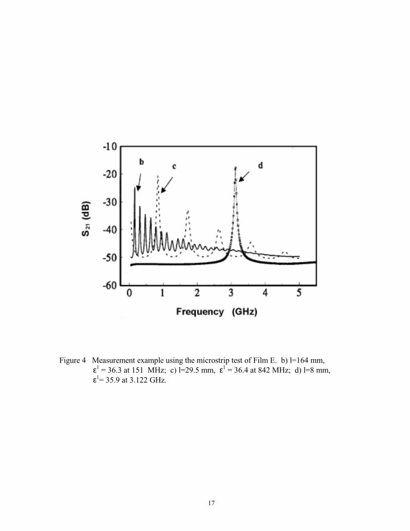
length l =164 mm, ε1 = 3.93 at 461 MHz) ………………………………. 16 Figure 4 Measurement example using the microstrip test of Film E. b) l=164 mm, ε1 = 36.3 at 151 MHz; c) l=29.5 mm, ε1 = 36.4 at 842 MHz; d) l=8 mm,
ε1= 35.9 at 3.122 GHz …………………………………………………… 17 Figure 5. Insulation resistance of Film A under bias of 100V as a function of
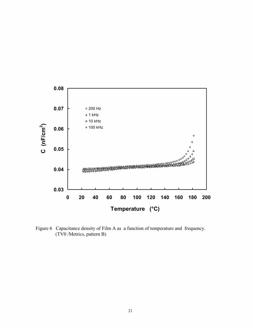
temperature ………………………………………………………………. 19 Figure 6 Capacitance density of Film A as a function of temperature and frequency.
(TV0 / Metrics, pattern B) ……………………………………………….. 21 Figure 7 Dielectric loss tangent of Film A as a function of temperature and frequency.
(TV0 / Metrics, pattern B) ………………………………………………... 22 Figure 8 Capacitance density of Film A saturated with moisture d during HAST.
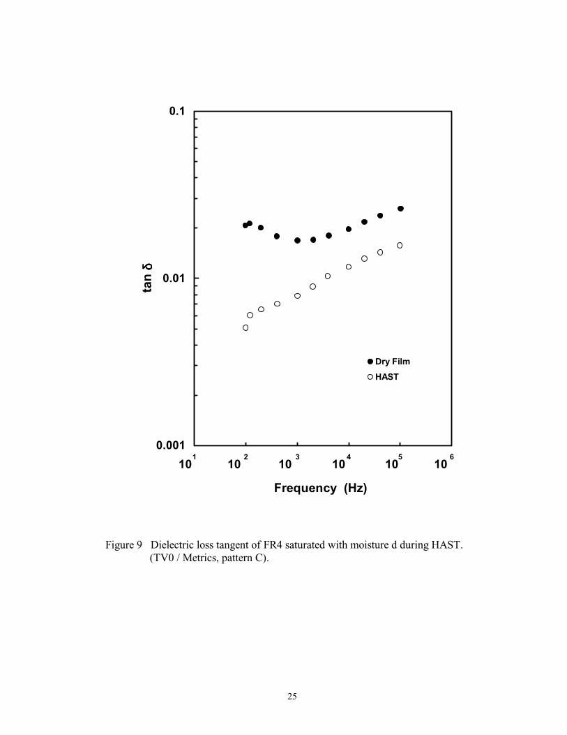
(TV0 / Metrics, pattern C) ………………………………………………… 24 Figure 9 Dielectric loss tangent of FR4 saturated with moisture d during HAST.
(TV0 / Metrics, pattern C) ………………………………………………… 25 Figure 10 Capacitance density of Film B as a function of temperature and frequency
(TV0, pattern B) …………………………………………………………... 28 Figure 11 Dielectric loss tangent of Film B as a function of temperature and frequency
(TV0, pattern B) ………………………………………………………….. 29 Figure 12 Capacitance density of Film C as a function of temperature and frequency.
(TV0, pattern B) ………………………………………………………….. 32 Figure 13 Dielectric loss tangent of Film C as a function of temperature and frequency.
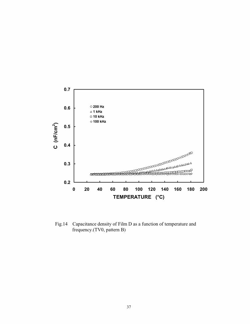
(TV0, pattern B) …………………………………………………………. 33 Figure 14 Capacitance density of Film D as a function of temperature and frequency.
(TV0, pattern B) …………………………………………………………. 37
5
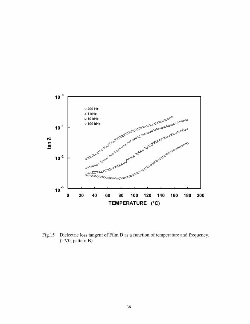
Figure 15 Dielectric loss tangent of Film D as a function of temperature and frequency. (TV0, pattern B) …………………………………………………………. 38
Figure 16 Capacitance density of Film E as a function of temperature and frequency.
(TV0, pattern B) ………..………………………………………………… 41 Figure 17 Dielectric loss tangent of Film E as a function of temperature and frequency.
(TV0, pattern B) …………………………………………………………. 42 Figure 18 Comparison of microwave dielectric thin Films ………………………. 45
6
LIST OF TABLES Table 1. Polymer Thin-Film Materials ……………………………………… 9 Table 2. High frequency dielectric constant of Film A ………………………. 23 Table 3. High frequency dielectric constant of Film B ………………………. 27 Table 4. High frequency dielectric constant of Film C ………………………. 31 Table 5. Dielectric Constant and Loss Tangent of Film D …………………… 36 Table 6. Dielectric Constant and Loss Tangent of Film Film E ……………… 40
7
Chapter 1
INTRODUCTION
Polymer-based high dielectric constant films (high-K) can be used to construct
embedded, discrete RLC circuits and decoupling power planes for use in wireless
communication and high-speed electronics. The permittivity of the prospective materials
should be high and determined with a high degree of confidence for operation at microwave
frequencies. In order to develop and successfully commercialize such materials, the industry
needs a suitable test method to measure dielectric properties and to assess the functional and
reliability performance of these materials in planar, thin film configuration. National Center
for Manufacturing Science (NCMS) has setup the Embedded Decoupling Capacitance
Consortium to study this problem. The objectives for National Institute of Standards and
Technology (NIST) involved in this NCMS-led project was to develop and evaluate a
practical material test method suitable for dielectric permittivity of high-k polymer composite
films that covers a broad frequency range including the microwave.
Currently, there are no standard test procedures for evaluating the electrical properties
of high relative dielectric constant films in the frequency range of practical importance viz.,
at low frequencies where charge storage is important and at microwave frequencies where
sub-nanosecond discharge rates are important. The current American Society for Testing and
Materials (ASTM) and The Institute for Interconnecting and Packaging Electronic Circuits
(IPC) test procedures are only suited for a narrow frequency range and are designed for large
samples. For example, ASTM D150, D669 and D1631 are for near 1 MHz, ASTM 3380,
IPC-TM-650 No. 2.5.5.5)2 are for frequencies from 8 GHz to12 GHz. We employed several
test patterns, specifically designed to evaluate the dielectric properties of high-k polymer
composite films that were used by the NCMS Embedded Distributed Capacitance Project.
The dielectric constant of the embedded capacitance materials was measured in the frequency
range of 100 Hz to 5 GHz. The testing also included evaluation of the capacitance density,
leakage current, and effect of highly accelerated temperature and humidity stress test,
(HAST) 3 on the capacitance. In this work, all dielectric constants are referred to the relative
dielectric constant of a material.
8
Chapter 2
POLYMER THIN-FILM MATERIALS
Five polymer thin-film materials are discussed in this report. They were designed for
the same application and prepared by microelectronic companies. All specimens are polymer
composites containing high dielectric constant ferroelectric powders. Each company uses
their own specific polymer and special powder to form their composite. Each company had
optimized the processing conditions for the specific composite material. However, all films
were processed in to the format according to our specifications for evaluation. The essential
information of the polymer composite thin-films supplied by the film providers are listed in
Table 1. For comparison, we have prepared a reference thin-film of FR4, Film A. FR4 is a
fiberglass epoxy laminate, of which we assume the dielectric properties are quite well
known. Film A has been prepared at same conditions.
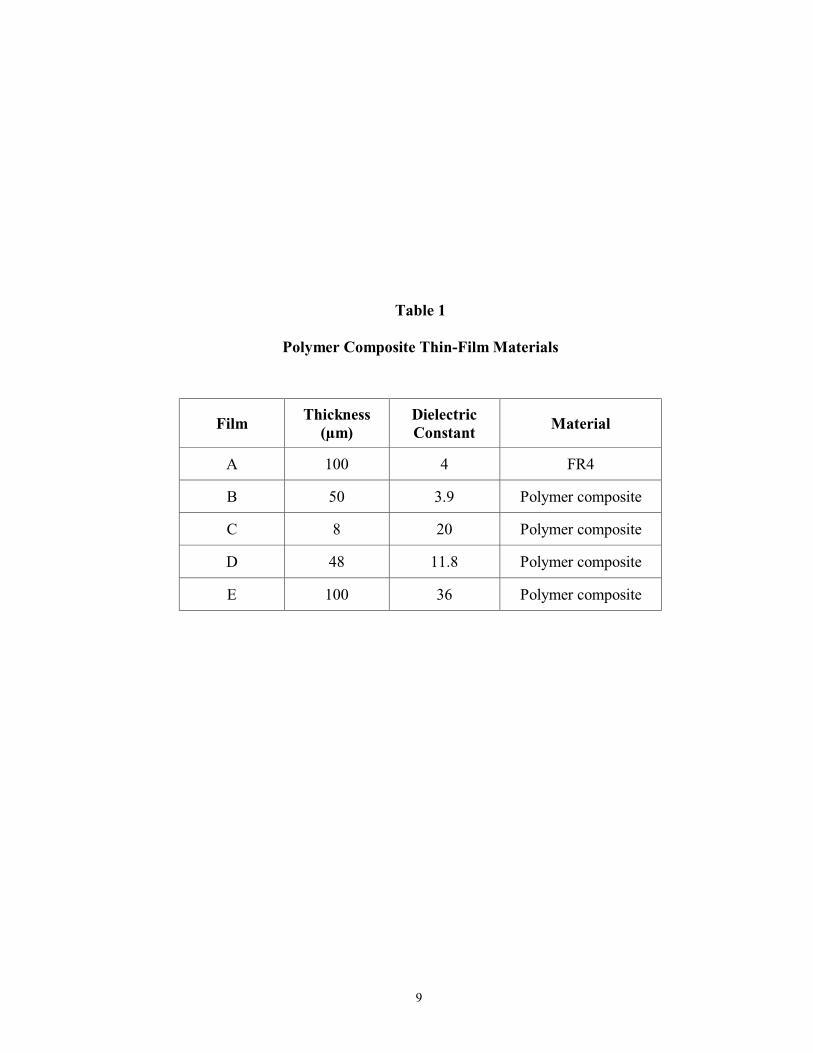
9
Table 1
Polymer Composite Thin-Film Materials
Film Thickness
(µm) Dielectric Constant
Material
A 100 4 FR4
B 50 3.9 Polymer composite
C 8 20 Polymer composite
D 48 11.8 Polymer composite
E 100 36 Polymer composite
10
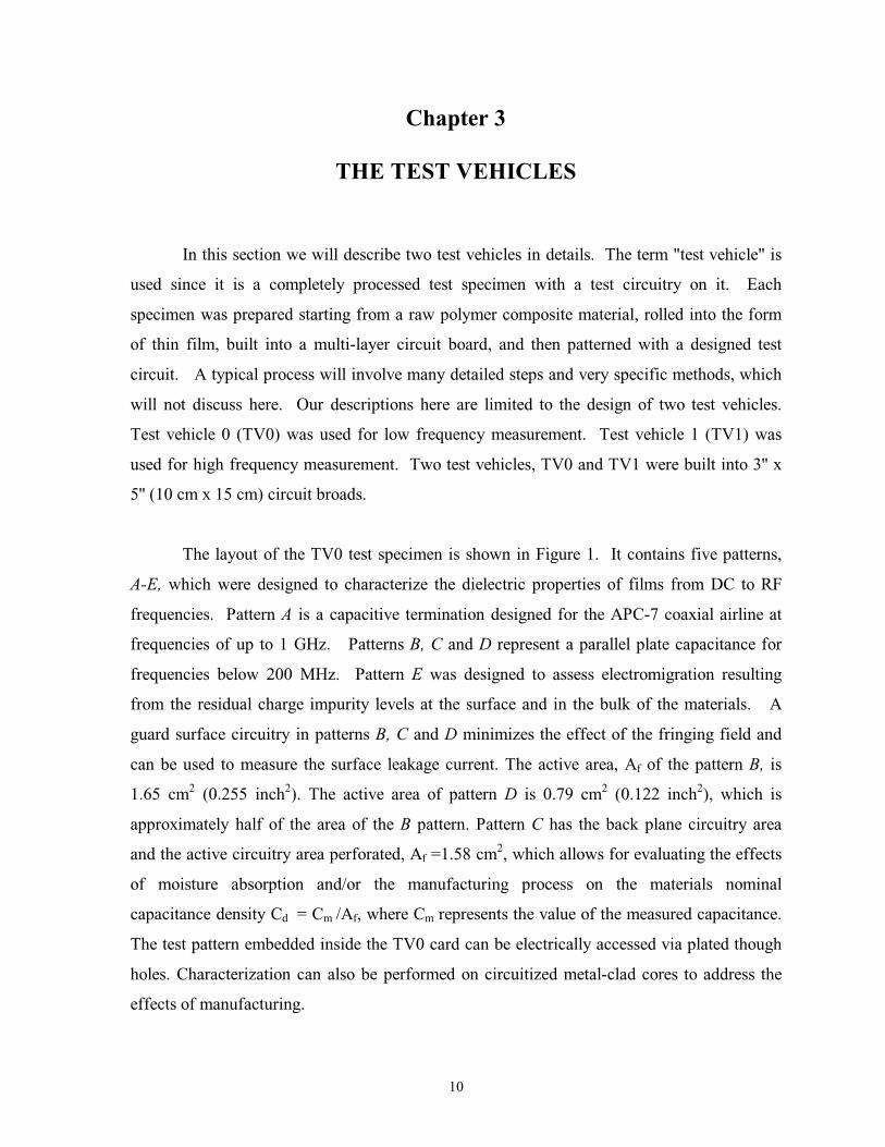
Chapter 3
THE TEST VEHICLES
In this section we will describe two test vehicles in details. The term "test vehicle" is
used since it is a completely processed test specimen with a test circuitry on it. Each
specimen was prepared starting from a raw polymer composite material, rolled into the form
of thin film, built into a multi-layer circuit board, and then patterned with a designed test
circuit. A typical process will involve many detailed steps and very specific methods, which
will not discuss here. Our descriptions here are limited to the design of two test vehicles.
Test vehicle 0 (TV0) was used for low frequency measurement. Test vehicle 1 (TV1) was
used for high frequency measurement. Two test vehicles, TV0 and TV1 were built into 3'' x
5'' (10 cm x 15 cm) circuit broads.
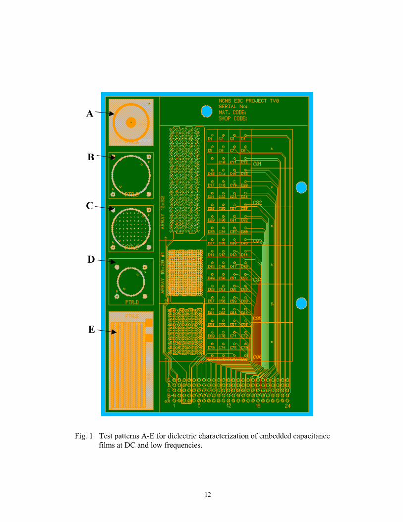
The layout of the TV0 test specimen is shown in Figure 1. It contains five patterns,
A-E, which were designed to characterize the dielectric properties of films from DC to RF
frequencies. Pattern A is a capacitive termination designed for the APC-7 coaxial airline at
frequencies of up to 1 GHz. Patterns B, C and D represent a parallel plate capacitance for
frequencies below 200 MHz. Pattern E was designed to assess electromigration resulting
from the residual charge impurity levels at the surface and in the bulk of the materials. A
guard surface circuitry in patterns B, C and D minimizes the effect of the fringing field and
can be used to measure the surface leakage current. The active area, Af of the pattern B, is
1.65 cm2 (0.255 inch2). The active area of pattern D is 0.79 cm2 (0.122 inch2), which is
approximately half of the area of the B pattern. Pattern C has the back plane circuitry area
and the active circuitry area perforated, Af =1.58 cm2, which allows for evaluating the effects
of moisture absorption and/or the manufacturing process on the materials nominal
capacitance density Cd = Cm /Af, where Cm represents the value of the measured capacitance.
The test pattern embedded inside the TV0 card can be electrically accessed via plated though
holes. Characterization can also be performed on circuitized metal-clad cores to address the
effects of manufacturing.
11
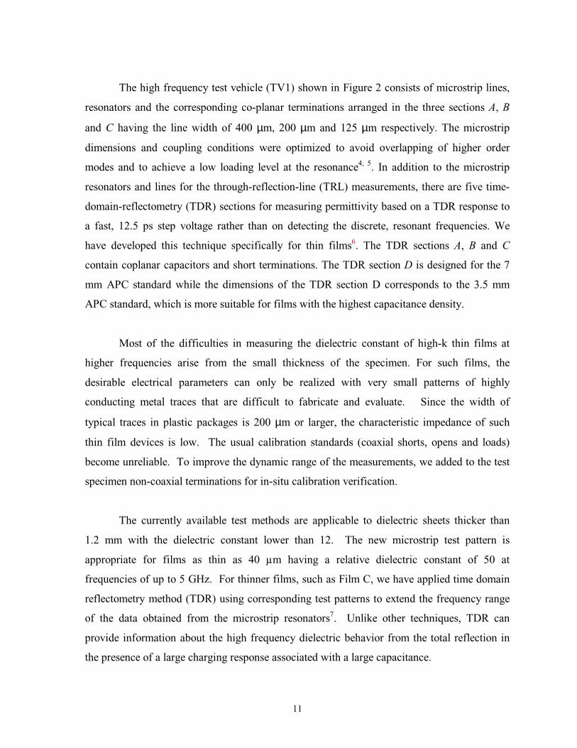
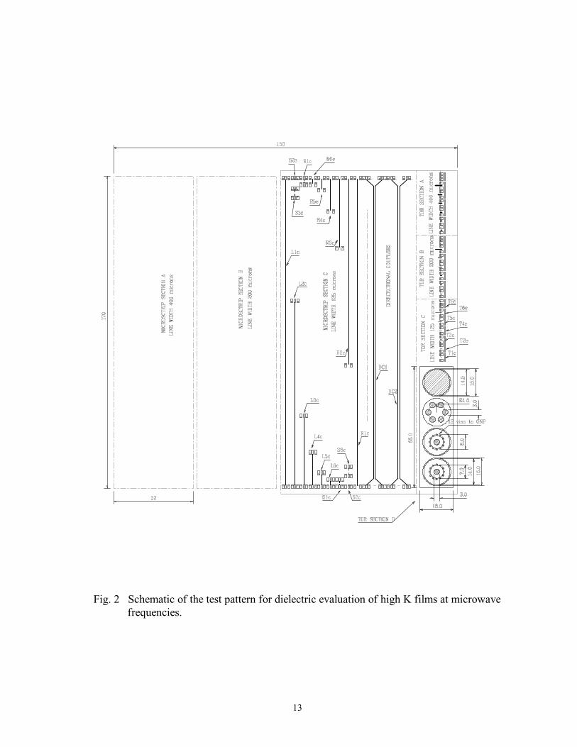
The high frequency test vehicle (TV1) shown in Figure 2 consists of microstrip lines,
resonators and the corresponding co-planar terminations arranged in the three sections A, B
and C having the line width of 400 µm, 200 µm and 125 µm respectively. The microstrip
dimensions and coupling conditions were optimized to avoid overlapping of higher order
modes and to achieve a low loading level at the resonance4, 5. In addition to the microstrip
resonators and lines for the through-reflection-line (TRL) measurements, there are five time-
domain-reflectometry (TDR) sections for measuring permittivity based on a TDR response to
a fast, 12.5 ps step voltage rather than on detecting the discrete, resonant frequencies. We
have developed this technique specifically for thin films6. The TDR sections A, B and C
contain coplanar capacitors and short terminations. The TDR section D is designed for the 7
mm APC standard while the dimensions of the TDR section D corresponds to the 3.5 mm
APC standard, which is more suitable for films with the highest capacitance density.
Most of the difficulties in measuring the dielectric constant of high-k thin films at
higher frequencies arise from the small thickness of the specimen. For such films, the
desirable electrical parameters can only be realized with very small patterns of highly
conducting metal traces that are difficult to fabricate and evaluate. Since the width of
typical traces in plastic packages is 200 µm or larger, the characteristic impedance of such
thin film devices is low. The usual calibration standards (coaxial shorts, opens and loads)
become unreliable. To improve the dynamic range of the measurements, we added to the test
specimen non-coaxial terminations for in-situ calibration verification.
The currently available test methods are applicable to dielectric sheets thicker than
1.2 mm with the dielectric constant lower than 12. The new microstrip test pattern is
appropriate for films as thin as 40 µm having a relative dielectric constant of 50 at
frequencies of up to 5 GHz. For thinner films, such as Film C, we have applied time domain
reflectometry method (TDR) using corresponding test patterns to extend the frequency range
of the data obtained from the microstrip resonators7. Unlike other techniques, TDR can
provide information about the high frequency dielectric behavior from the total reflection in
the presence of a large charging response associated with a large capacitance.
12
Fig. 1 Test patterns A-E for dielectric characterization of embedded capacitance
films at DC and low frequencies.
A
B
C
D
E
13
Fig. 2 Schematic of the test pattern for dielectric evaluation of high K films at microwave
frequencies.
14
Chapter 4
EXPERIMENTAL
The low frequency measurements were carried out in accordance to the ASTM D-150
standard test method1 using a HP4274A / HP4282A Impedance Analyzer. The
measurements were performed on TV0 patterns B and C and D. The instrumental
reproducibility of measurement of complex capacitance is less than 0.5 % of the measured
value. The effect due to measurement of the fringing field was negligible since the electrical
configuration included a guarding electrode. The uncertainty in the measurement of the
electrode size and film thickness was estimated to be about 4 % of the data. The combined
standard uncertainties of low frequency dielectric constant and tan δ listed in Tables 1 to
Table 5 are about 5 % of the reported value.
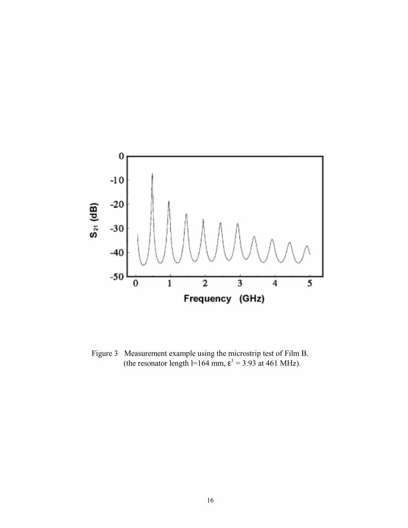
Measurements in the high frequency range were performed using the high frequency
test vehicle (TV1, Figure 2) on several microstrip test specimens fabricated to fine
dimensions using photolithography. The resonant frequencies were detected by measuring
the S2,1 parameters using a HP 8720D Network Analyzer and Cascade ACP-40-W GSG
probes. Example results are shown in Figure 3 and Figure 4. The temperature-dependent
measurements were carried out in the EC-12 Environmental Chamber from Sun
Microsystems. The relative dielectric constant, εr, was calculated from the following
formula4
+
=
22
2,
2
22 wn
lm
f
c
nmrεεεε
where l and w are the electrical length and width of the resonator, m and n are the mode
integers. The dielectric loss was estimated from the width of the resonance peak, measured 3
dB below its maximum value. The largest contribution to the uncertainty in this method
comes from the coupling length, which affects the total length of the resonator. The
15
combined standard uncertainty of high frequency dielectric constant and tan δ listed In Table
1 to Table 5 increases from about 2 % at 1 GHz, to 8 % of the value at 5 GHz. The
capacitance and tan δ data shown in the form of figure in the result section has the same
uncertainty as discussed here.
16
Figure 3 Measurement example using the microstrip test of Film B. (the resonator length l=164 mm, ε1 = 3.93 at 461 MHz).
17
Figure 4 Measurement example using the microstrip test of Film E. b) l=164 mm,
ε1 = 36.3 at 151 MHz; c) l=29.5 mm, ε1 = 36.4 at 842 MHz; d) l=8 mm, ε1= 35.9 at 3.122 GHz.
18
Chapter 5
RESULTS AND DISCUSSION
The five film capacitance materials listed in Chapter 2 were evaluated. For
comparison, data was interpreted in terms of that obtained for the FR4 fiberglass epoxy
laminate in analogous conditions. The low frequency measurements were performed on TV0
pattern B and C.
Polymer Film A
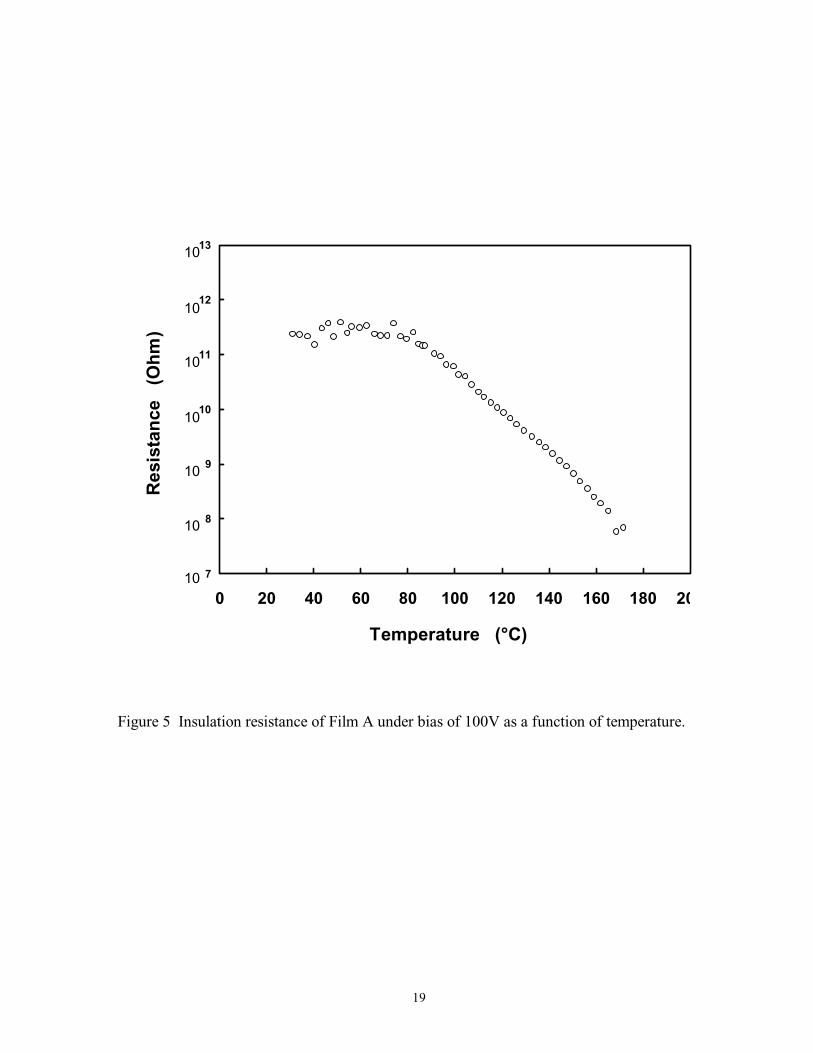
Figure 5 shows the DC insulation resistance of FR4 material under 100 V bias as a
function of temperature. The insulation resistance decreases from about 1 x 10¹¹ Ω at 85 °C
to 5 x 10⁷ Ω at 180 °C, indicating an excellent electrical insulation characteristic.
The capacitance density and the dielectric loss tangent of the FR4 material as a
function of frequency and temperature are shown in Figure 6 and Figure 7, respectively. In
the glassy state, below 125 °C, FR4 shows a relatively insignificant dependence of the
capacitance on frequency, which reflects the behavior of the dielectric constant of he material
(referred as dielectric dispersion). Following the dielectric dispersion, the capacitance
density decreases slightly with increasing frequency. In the temperature range of 20 °C to
about 130 °C, the capacitance density is approximately 0.04 nF/cm2. Above 130 °C, the FR4
resin enters the rubbery state and the capacitance increases considerably due to the liberation
of large-sack motions of the resin backbone. This molecular behavior is also responsible for
an increase in the dielectric loss tangent at temperatures approaching the glass-rubber
transition. It is noteworthy that the low frequency loss tangent measurements detect the
beginning of the glass-rubber relaxation process at temperature typically (10 to 15) °C below
the Tg determined by the DSC or TMMA techniques. The 200 Hz curve in Figure 7
exhibits a low temperature shoulder of the α-relaxation peak, which shifts to higher
temperatures as the
19
7
8
9
10
11
12
13
0 20 40 60 80 100 120 140 160 180 20
Temperature (°C)
Res
ista
nce
(O
hm
)
10
10
10
10
10
10
10
Figure 5 Insulation resistance of Film A under bias of 100V as a function of temperature.
20
frequency increases. In other words, the dielectric loss at elevated temperatures appears to
decrease as the frequency increases.
In addition to the α relaxation, FR4 also exhibits a local β-relaxation, which strongly
affects the dielectric performance of the material in the RF and microwave frequency range.
A high temperature shoulder of the β-relaxation peak is seen on the 100 kHz curve in Figure
7 as a decrease in the dielectric loss in the temperature range of 20 °C to about 140 °C. This
peak shifts to lower temperatures with decreasing frequency. Therefore, the room
temperature dielectric loss in Figure 7 appears to increase with increasing frequency. For a
typical FR4 resin, the room temperature dielectric loss tangent reaches a maximum of about
0.025 at 10 MHz. The loss due to β relaxation should decrease at higher frequencies (room
temperature) though molecular defects, free radicals and other paramagnetic impurities may
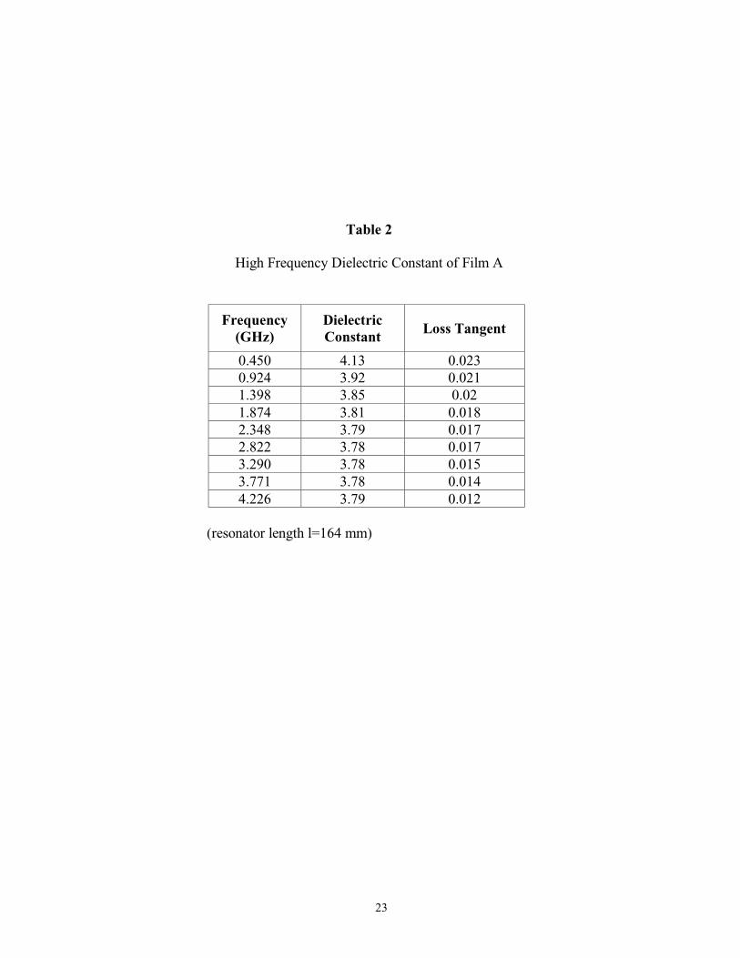
contribute to the dielectric loss mechanism, extending it into the microwave. The dielectric
constant data in the high frequency range obtained for FR4 using the microstrip test pattern is
given in Table 2.
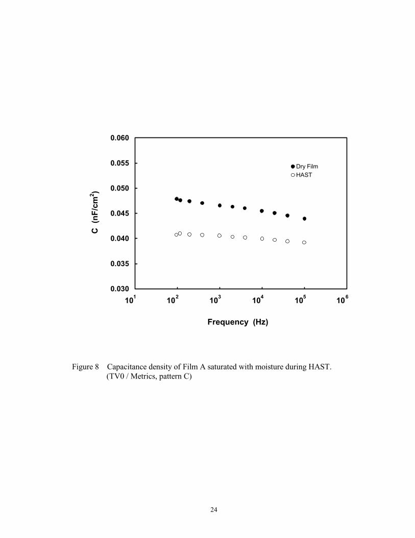
Moisture absorbed during a HAST test increases the dielectric loss and the dielectric
constant (capacitance density). The largest effect is seen at the lowest frequencies (Fig 8)
due to interfacial polarization. At 200 Hz, the change in capacitance after HAST is about 6
pF/cm2. In comparison, the dielectric loss tangent increases considerably higher: from 7 x
10-3 to about 2 x 10⁻². This indicates that the absorbed water may facilitate electromigration
and compromise the reliability of the dielectric under DC bias or when carrying a digital
ON/OFF signal.
21
0.03
0.04
0.05
0.06
0.07
0.08
0 20 40 60 80 100 120 140 160 180 200
Temperature (°C)
C (
nF
/cm
2 )
200 Hz
1 kHz
10 kHz
100 kHz
Figure 6 Capacitance density of Film A as a function of temperature and frequency. (TV0 /Metrics, pattern B)
22
0.001
0.01
0.1
1
0 20 40 60 80 100 120 140 160 180 200
Temperature (°C)
tan
δ δδδ
200 Hz1 kHz10 kHz100 kHz
Figure 7 Dielectric loss tangent of Film A as a function of temperature and
frequency.(TV0 / Metrics, pattern B)
23
Table 2
High Frequency Dielectric Constant of Film A
Frequency (GHz)
Dielectric Constant
Loss Tangent
0.450 4.13 0.023 0.924 3.92 0.021 1.398 3.85 0.02 1.874 3.81 0.018 2.348 3.79 0.017 2.822 3.78 0.017 3.290 3.78 0.015 3.771 3.78 0.014 4.226 3.79 0.012
(resonator length l=164 mm)
24
0.030
0.035
0.040
0.045
0.050
0.055
0.060
1 2 3 4 5 6
Frequency (Hz)
C (
nF
/cm
2 )
Dry FilmHAST
10 1010101010
Figure 8 Capacitance density of Film A saturated with moisture during HAST. (TV0 / Metrics, pattern C)
25
0.001
0.01
0.1
1 2 3 4 5 6
Frequency (Hz)
tan
δ δδδ
Dry Film
HAST
10 1010101010
Figure 9 Dielectric loss tangent of FR4 saturated with moisture d during HAST. (TV0 / Metrics, pattern C).
26
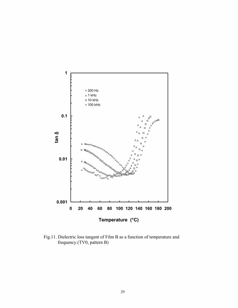
POLYMER FILM B
The DC insulation resistance of the Film B shows a thermally activated behavior
similar to that of FR4 (Fig 5). The insulation resistance decreases from about 1 x 10¹¹ Ω at
85 °C to 1 x 10⁷ Ω at 180 °C. A change in the activation energy of the conducting process
takes place at about 125 °C due to glass-rubber transition of the resin. The capacitance
density is about 0.08 nF/cm2, (0.5 nF/inch2) approximately twice that observed in the FR4.
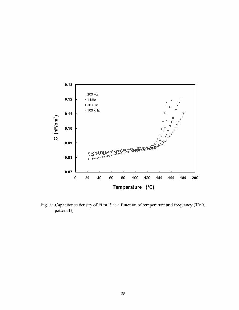
This is due to the decrease in thickness of the dielectric. The capacitance density and the
dielectric loss tangent plots shown in Figures 10 and 11 for Film B as a function of frequency
and temperature are analogous to that of FR4 (Figures 6 and 7).
The dependence of capacitance density (the dielectric constant) on temperature is
somewhat stronger than that of FR4, probably due to lower glass transition temperature.
Consequently, both the large-sack and local relaxation are more temperature dependent,
which contributes to an increase in loss at the RF and microwave range. The dielectric
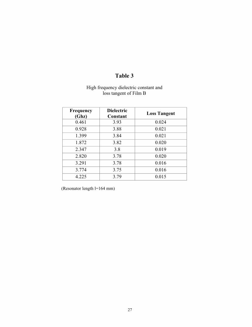
constant data in the high frequency range obtained for Film B using the microstrip test
pattern is given in Table 3.
Saturation with moisture during HAST increases capacitance density by about 3
pF/cm2 from 0.081nF/cm2 to 0.084 nF/cm2. Moisture also contributes to an increase in the
dielectric loss. The large effects were similar to those shown in Figs. 8 and 9 for FR4 at the
lowest frequencies.
27
Table 3
High frequency dielectric constant and loss tangent of Film B
Frequency (Ghz)
Dielectric Constant
Loss Tangent
0.461 3.93 0.024 0.928 3.88 0.021 1.399 3.84 0.021 1.872 3.82 0.020 2.347 3.8 0.019 2.820 3.78 0.020 3.291 3.78 0.016 3.774 3.75 0.016 4.225 3.79 0.015
(Resonator length l=164 mm)
28
0.07
0.08
0.09
0.10
0.11
0.12
0.13
0 20 40 60 80 100 120 140 160 180 200
Temperature (°C)
C (
nF
/cm
2 )
200 Hz
1 kHz
10 kHz
100 kHz
Fig.10 Capacitance density of Film B as a function of temperature and frequency (TV0,
pattern B)
29
0.001
0.01
0.1
1
0 20 40 60 80 100 120 140 160 180 200
Temperature (°C)
tan
δ δδδ
200 Hz1 kHz10 kHz100 kHz
Fig.11. Dielectric loss tangent of Film B as a function of temperature and
frequency.(TV0, pattern B)
30
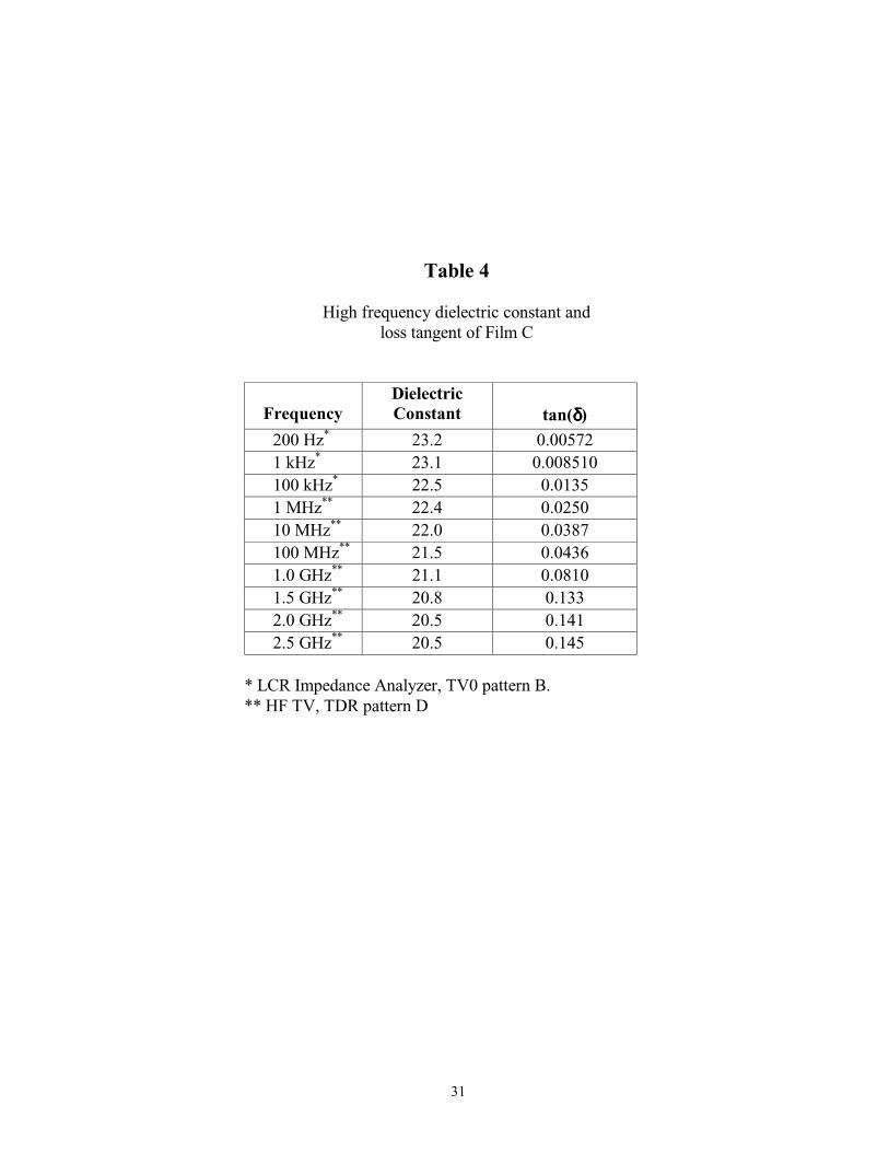
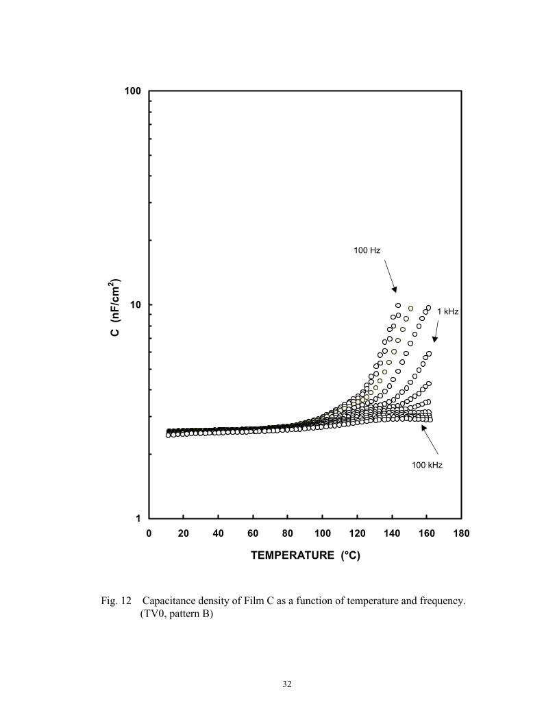
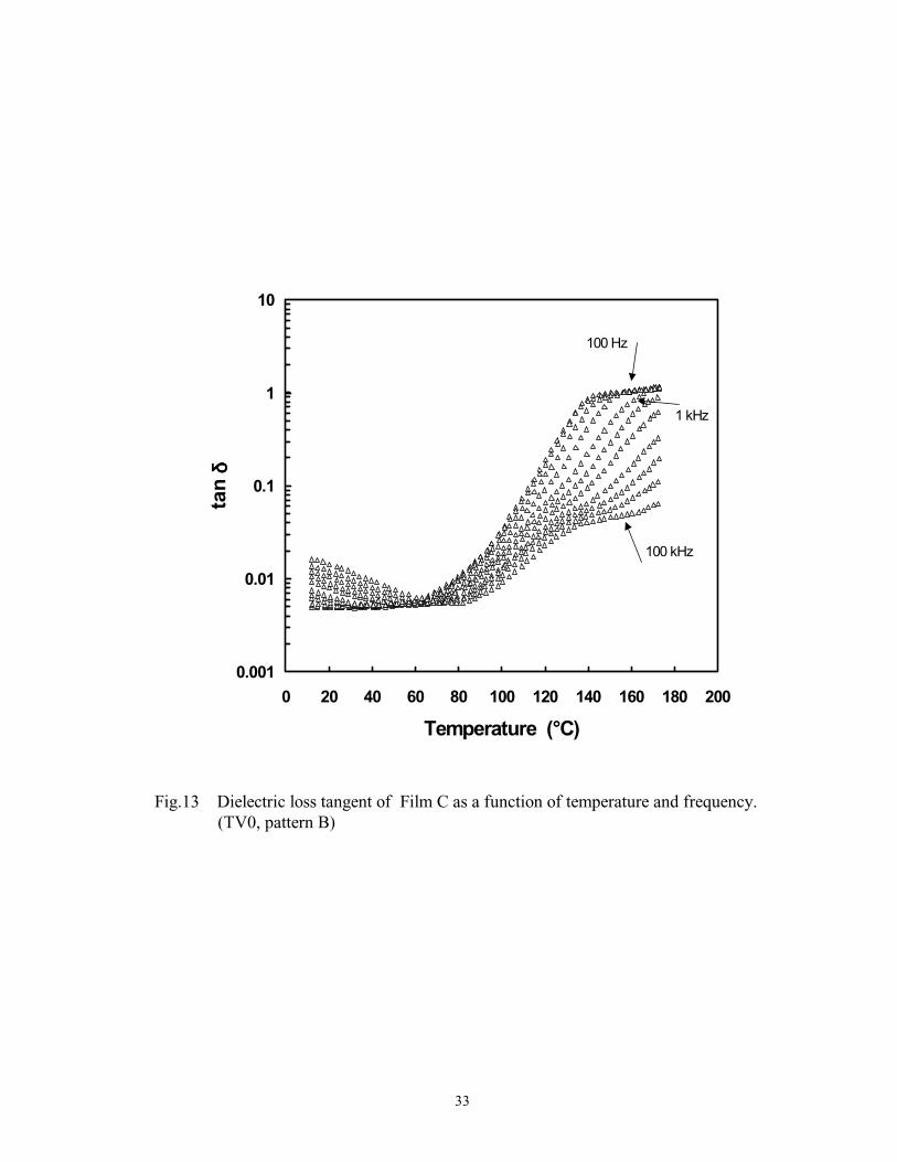
Polymer Film C
The capacitance density of the Film C, 8 µm thick films were determined to be about
2.5 nF/cm2 (16 nF/inch2) at ambient conditions. The material shows a depressive behavior,
similar to that of epoxy-based composites. The capacitance density and the dielectric loss
tangent plots are shown in Figures 12 and 13 as a function of temperature at several
frequencies. A thermally activated increase in capacitance is seen above 85 °C (Figure 12).
The data in Figure 12 and 13 is reminiscent of a resin blend that has a glass transition
temperature below 130 °C. Therefore, the temperature dependence of capacitance density
(dielectric constant) is stronger than of FR4 and both the large sack and local relaxation are
more temperature dependent. This is evidenced as an increase in the dielectric loss. The
dielectric constant at high frequencies, above 1 MHz, was measured using the TDR
technique (Table 4). Due to the small thickness and large capacitance, the 400 µm wide
microstrip lines exhibited very low impedance, below 2 Ω, causing a large return loss (S11) at
the input reference plane. Therefore, the resonance peaks were diminished and analysis
difficult, especially at frequencies above 1 GHz. In contrast, the TDR method was more
suitable for determination of the dielectric constant in the presence of large charging currents.
The results obtained at the ambient temperature are listed in Table 4. It is seen that Film C
exhibits relatively low dispersion. The dielectric constant decreases slightly from 23 at 200
Hz to 20.5 at 2 GHz. The dielectric loss tangent increases from 0.005 to about 0.14 in the
same frequency range. At 1 GHz, Film C exhibited the largest loss among the investigated
materials.
31
Table 4
High frequency dielectric constant and
loss tangent of Film C
Frequency
Dielectric Constant
tan(δδδδ)
200 Hz* 23.2 0.00572 1 kHz* 23.1 0.008510 100 kHz* 22.5 0.0135 1 MHz** 22.4 0.0250 10 MHz** 22.0 0.0387 100 MHz** 21.5 0.0436 1.0 GHz** 21.1 0.0810 1.5 GHz** 20.8 0.133 2.0 GHz** 20.5 0.141 2.5 GHz** 20.5 0.145
* LCR Impedance Analyzer, TV0 pattern B. ** HF TV, TDR pattern D
32
1
10
100
0 20 40 60 80 100 120 140 160 180
TEMPERATURE (°C)
C (
nF
/cm
2 )
100 Hz
100 kHz
1 kHz
Fig. 12 Capacitance density of Film C as a function of temperature and frequency.
(TV0, pattern B)
33
0.001
0.01
0.1
1
10
0 20 40 60 80 100 120 140 160 180 200
Temperature (°C)
tan
δ δδδ
100 Hz
1 kHz
100 kHz
Fig.13 Dielectric loss tangent of Film C as a function of temperature and frequency.
(TV0, pattern B)
34
Polymer Film D
The insulation resistance of Film D decreases with increasing temperature
exponentially from about 3 x 10⁹ Ω at 85 °C to 5 x 10⁶ Ω at 180 °C. In contrast to the
epoxy-based composites, which undergo a glass-rubber transition at about 130 °C, the
thermally activated DC conductivity of Film D in the glassy state has single activation
energy. The capacitance density is about 0.25 nF/cm2, which corresponds to the dielectric
constant 12 for films of 41 µm in thickness at ambient temperatures.
Figures 14 and 15 shows the effect of temperature on the capacitance density and the
dielectric loss tangent at several frequencies from 200 Hz to 100 kHz. At ambient conditions
the capacitance density is about 0.25 nF/cm2 (1.5 nF/inch2) without noticeable dispersion, i.e.
no frequency dependence. The capacitance density increases with temperature only at
frequencies below 10 kHz. This behavior probably originates from the interfacial
arrangement and polarization between separate phases in the composite rather than from
polarization of the polyimide backbone itself. It is seen that at higher frequencies, above 10
kHz, the capacitance density appears to be independent of temperature. This is in contrast to
the epoxy-based composites, which typically show thermally activated increase in
capacitance when the rubbery transition of the resin is approached. It is worthy to note that
the dielectric loss tangent decreases with increasing frequency.
At room temperature, Figure 15, the dielectric loss tangent decreases from
approximately 0.01 at 200 Hz to 0.002 at 1 MHz (Table 5). In comparison, the epoxy-based
composite films show an increasing loss at similar frequencies and temperatures. The
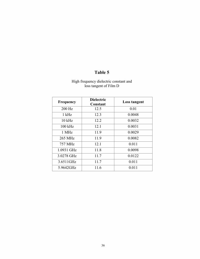
dielectric data of high-k polyimide at higher frequencies is listed in Table 5 where the
dielectric constant decreases from 12.5 at 200 Hz to about 11.6 at 6 GHz. An apparent
increase in the dielectric loss tangent at frequencies of 265 MHz and above may be the result
of electrical limitations of the microstrip test specimen (limited Q factor) at higher
frequencies.
35
Saturation with moisture during HAST increases capacitance density and loss of
Film D considerably. The effect is especially large at the lowest frequencies and might be
due to interfacial polarization and accumulation of charge carriers between the polyimide
resin and the ceramic phases. At 200 Hz, 25 °C, the difference in capacitance density
between the dry and moisture-saturated samples was about 120 pF/cm2.
36
Table 5
High frequency dielectric constant and loss tangent of Film D
Frequency Dielectric Constant
Loss tangent
200 Hz 12.5 0.01
1 kHz 12.3 0.0048
10 kHz 12.2 0.0032
100 kHz 12.1 0.0031
1 MHz 11.9 0.0029
265 MHz 11.9 0.0082
757 MHz 12.1 0.011
1.0931 GHz 11.8 0.0098
3.0278 GHz 11.7 0.0122
3.6511GHz 11.7 0.011
5.9642GHz 11.6 0.011
37
0.2
0.3
0.4
0.5
0.6
0.7
0 20 40 60 80 100 120 140 160 180 200
TEMPERATURE (°C)
C (
nF
/cm
2 )
200 Hz1 kHz10 kHz100 kHz
Fig.14 Capacitance density of Film D as a function of temperature and frequency.(TV0, pattern B)
38
-3
-2
-1
0
0 20 40 60 80 100 120 140 160 180 200
TEMPERATURE (°C)
tan
δ δδδ
200 Hz1 kHz10 kHz100 kHz
10
10
10
10
Fig.15 Dielectric loss tangent of Film D as a function of temperature and frequency.
(TV0, pattern B)
39
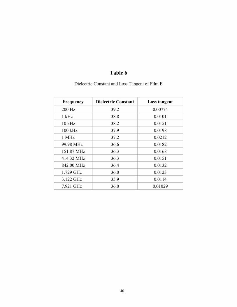
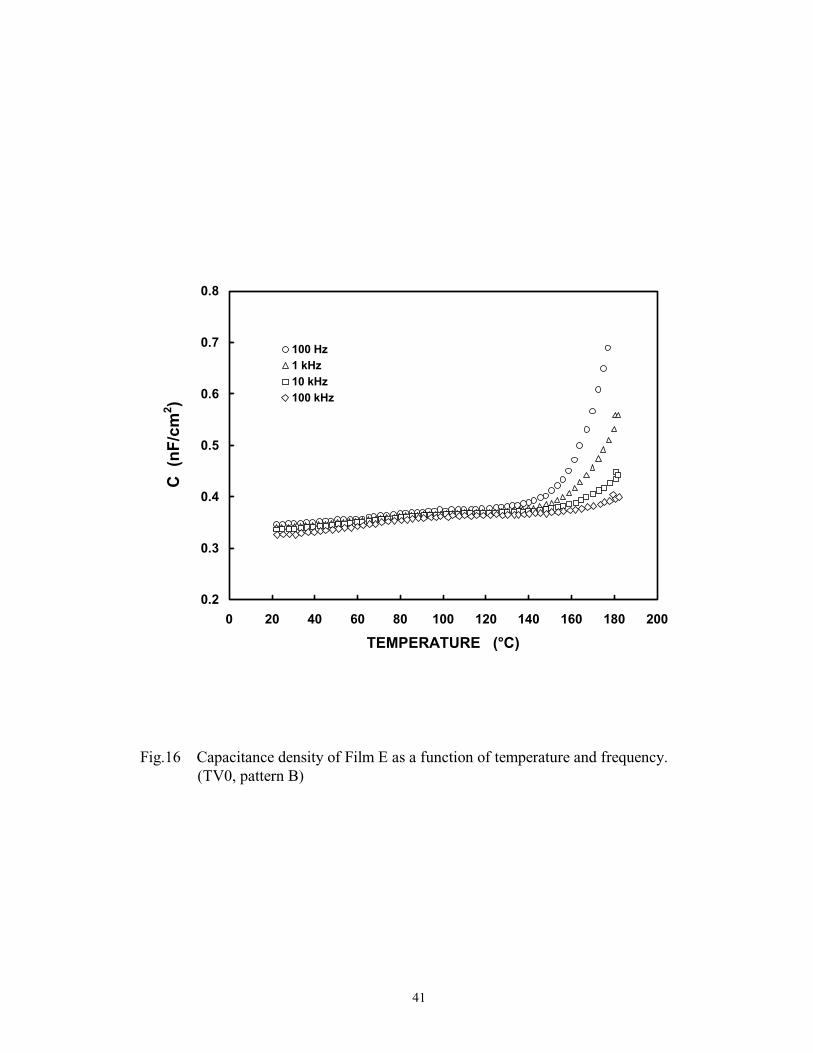
Polymer Film E
The DC insulation resistance of Film E shows a thermally activated behavior similar
to that seen in Figure 5 for FR4. The insulation resistance decreases from about 1011 Ω at 85
°C to 107 Ω at 180 °C. A change in the activation energy of the conducting process was
detected at about 125 °C, which originated from the glass-rubber transition of the resin
matrix.
The capacitance density measured at ambient temperature was about 0.33nF/cm2 (2.1
nF/inch2), which for films 100 µm thick corresponds to a dielectric constant of about 37.
This is one of the highest dielectric constant values measured for an epoxy composite loaded
with ferroelectric powder. Since the practically achievable loading level is a volume faction
of about 50 % of the ceramic powder phase, the BaTiO3 powder-epoxy composites may
exhibit a dielectric constant about 50. The capacitance density and the dielectric loss tangent
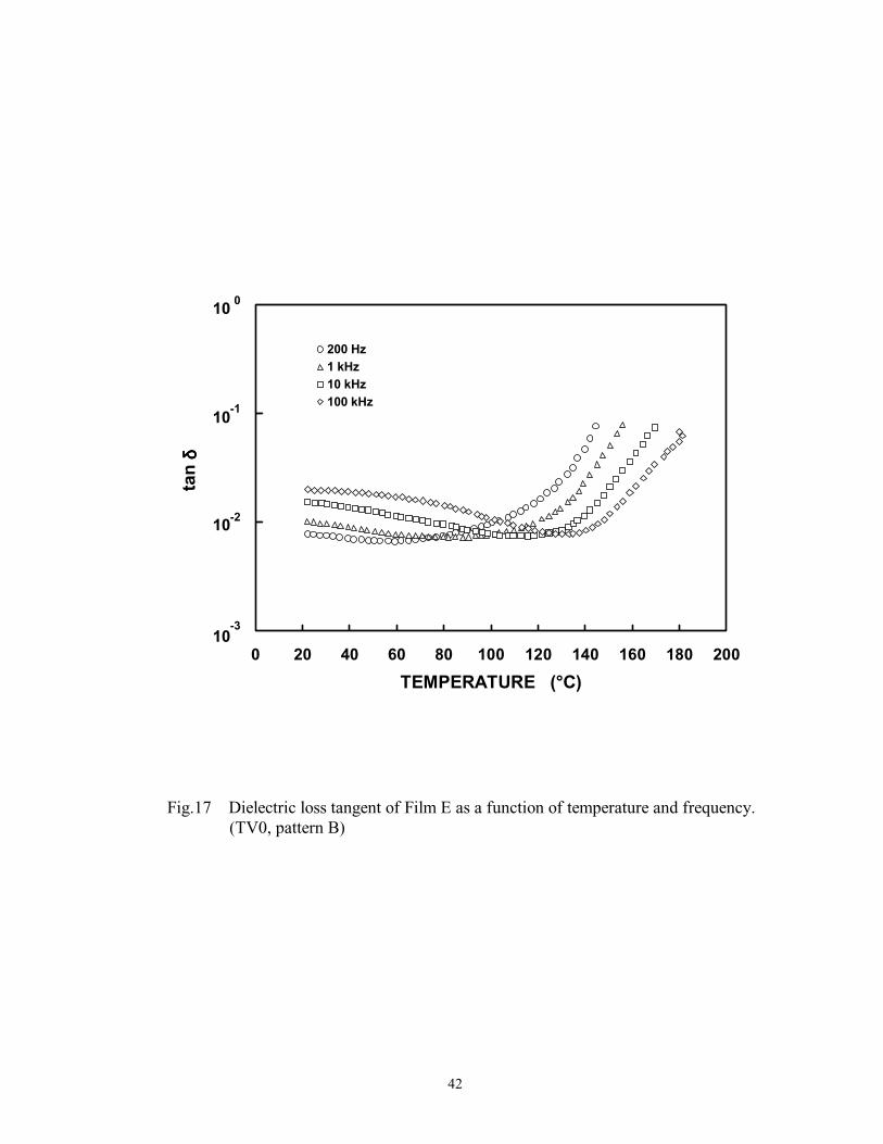
plots as a function of temperature at several frequencies are shown in Figure 16 and 17. A
thermally activated increase in capacitance is seen above 130 °C (Figure 16). The character
of the dielectric loss data is reminiscent of the FR4 epoxy resin laminates. This indicates
that the organic matrix rather than the high dielectric constant ceramic filler dictate the
dielectric loss. Thus, an increase in the dielectric loss with increasing frequency seen at
room temperature originates from the relaxation processes in the polymer.
Table 6 lists the room temperature dielectric constant and loss obtained for Film E using
the low frequency pattern B (200 Hz to 1 MHz) and the microstrip test pattern (100 MHz to 8
GHz). Saturation with moisture during the 200 h HAST increases the capacitance density.
At 200 Hz and 25 °C, the difference in capacitance density between the dry and moisture-
saturated samples was measured to be about 70 pF/cm2. Moisture absorption also
contributed to an increase in the dielectric loss. The effect was somewhat larger than that
shown in Figs. 8 and 9 for FR4.
40
Table 6
Dielectric Constant and Loss Tangent of Film E
Frequency Dielectric Constant Loss tangent
200 Hz 39.2 0.00774
1 kHz 38.8 0.0101
10 kHz 38.2 0.0151
100 kHz 37.9 0.0198
1 MHz 37.2 0.0212
99.98 MHz 36.6 0.0182
151.87 MHz 36.3 0.0168
414.32 MHz 36.3 0.0151
842.00 MHz 36.4 0.0132
1.729 GHz 36.0 0.0123
3.122 GHz 35.9 0.0114
7.921 GHz 36.0 0.01029
41
0.2
0.3
0.4
0.5
0.6
0.7
0.8
0 20 40 60 80 100 120 140 160 180 200
TEMPERATURE (°C)
C (
nF
/cm
2 )
100 Hz1 kHz10 kHz100 kHz
Fig.16 Capacitance density of Film E as a function of temperature and frequency.
(TV0, pattern B)
42
-3
-2
-1
0
0 20 40 60 80 100 120 140 160 180 200
TEMPERATURE (°C)
tan
δ δδδ
200 Hz1 kHz10 kHz100 kHz
10
10
10
10
Fig.17 Dielectric loss tangent of Film E as a function of temperature and frequency.
(TV0, pattern B)
43
Chapter 6
SUMMARY
Dielectric characterization of embedded capacitance materials has been done as a
function of temperature at frequencies ranging from 200 Hz to 5 GHz. The measurements of
the dielectric constant were performed in a practical, functional, thin film configuration using
test specimens specifically designed for the NCMS-led Embedded Capacitance Project. The
test specimens were fabricated using standard copper circuitize and card lamination
processes by participant companies.
The largest dielectric constant was measured for Film E. At 1 GHz this material
showed a dielectric constant of 36. The capacitance density of a 100 µm thick Film E was
about 0.33 nF/cm2 (2.1 nF/inch2). Film C showed at 1 GHz a dielectric constant of 20. In
comparison, the capacitance density of the 8 µm thick Film C was about 2.5 nF/cm2
(16 nF/inch2) nearly 8 times larger than that of Film E due to much smaller thickness of the
dielectric film. At frequency of 1 GHz, the dielectric constant of the Film D was about 11.8,
while the capacitance density of the 48 µm thick film was comparable to that of Film E,
about 0.25 nF/cm2 (1.5 nF/inch2). Film B exhibited the lowest dielectric constant, 3.9 and
the lowest capacitance density 0.08 nF/cm2 (0.5 nF/inch2) among the evaluated materials for
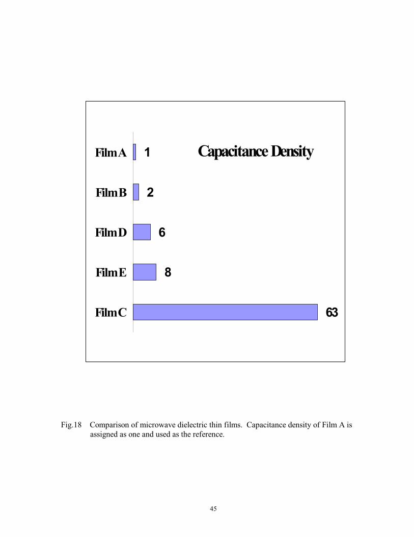
50 µm-thick films. Using the capacitance density of FR4 laminate as a reference, we
arranged the tested materials in the order of increasing the capacitance density as shown in
Figure 18. Our conclusion is that the capacitance density of the Film C was 63 times larger
than that of FR4. This is the state of art high dielectric constant film can be made by
industries if a material required today.
During heating, Films E, C and B showed a thermally activated increase in
capacitance and dielectric loss, similar to that of FR4 epoxy resin when the glass transition
temperature is approached. In contrast, permittivity of the Film D was much less
temperature dependent, especially at higher frequencies.
44
The dielectric properties of all the tested thin film capacitance composites are
sensitive to moisture. Water accumulated during HAST typically increase the capacitance
density and the dielectric loss tangent. The largest effect was observed at lowest frequencies
due to moisture-activated conductivity and interfacial polarization.
The high frequency microstrip test pattern with 400 µm wide traces was appropriate
for testing high-k films thicker than 40 µm at frequencies of up to 5 GHz. We are
investigating the applicability of higher impedance, narrower traces (250 µm and 125 µm
wide) for films thinner than 40 µm.
45
Fig.18 Comparison of microwave dielectric thin films. Capacitance density of Film A is
assigned as one and used as the reference.
63
8
6
2
1Film A
Film B
Film D
Film E
Film C
Capacitance Density
46
ACKNOWLEDGMENT
This work was supported in part by the NIST Advanced Technology Program. We
like to acknowledge the members of National Center for Manufacturing Science for
providing the test specimens.
47
DISCLAIMER
Certain materials and equipment identified in this manuscript are solely for specifying
the experimental procedures and do not imply endorsement by NIST or that they are
necessarily the best for these purposes.
48
REFERENCES 1. ASTM D150, D669, IPC TM-650, 2.5.5.1-9, “Permittivity (dielectric constant) and loss
tangent (dissipation factor) of insulating materials”, Rev. 5/86. 2. ASTM 3380, IPC TM-650, 2.5.5.5, “Stripline test for complex permittivity of circuit
board materials to 14 GHz”, Rev. 5/97. 3. JEDEC STANDARD No. 22-A110 Highly-Accelerated Temperature and Humidity
Stress Test, condition C. The sample was placed at 130 °C and 85% relative humidity for 200 hours.
4. P. H. Ladbrooke, M. H. N. Potok, and E. H. England, “Coupling errors in cavity-
resonance measurements on MIC dielectrics”, IEEE Trans., vol. MTT-21, pp 560-562, (1973).
5. K. C. Gupta, R. Garg, I. Bahl and P. Bhartia, Microstrip Lines and Slot lines, Artech
House, Boston, 1996. 6. R. Nozaki and J. Obrzut, “Microwave permittivity measurements of dielectric films using
TDR”, International Union of radio Science Conference, URSI-2000, pp 134, January 4 – 8, 2000 Boulder, Colorado.
7. J. Obrzut and R. Nozaki, “Permittivity measurements of high dielectric constant films at
microwave frequencies” IPC EXPO 2000, April 2-6, 2000, San Diego CA.
49
This page is just for information . Do Not Use. 1 ASTM D150, D669, IPC TM-650, 2.5.5.1-9, “Permittivity (dielectric constant) and loss
tangent (dissipation factor) of insulating materials”, Rev. 5/86. 2 ASTM 3380, IPC TM-650, 2.5.5.5, “Stripline test for complex permittivity of circuit
board materials to 14 GHz”, Rev. 5/97. 3 JEDEC STANDARD No. 22-A110 Highly-Accelerated Temperature and Humidity
Stress Test, condition C. The sample was placed at 130 °C and 85% relative humidity for 200 hours.
4 P. H. Ladbrooke, M. H. N. Potok, and E. H. England, “Coupling errors in cavity-resonance measurements on MIC dielectrics”, IEEE Trans., vol. MTT-21, pp 560-562, (1973).
5 K. C. Gupta, R. Garg, I. Bahl and P. Bhartia, Microstrip Lines and Slot lines, Artech House, Boston, 1996.
6 R. Nozaki and J. Obrzut, “Microwave permittivity measurements of dielectric films using TDR”, International Union of radio Science Conference, URSI-2000, pp 134, January 4 – 8, 2000 Boulder, Colorado.
7 J. Obrzut and R. Nozaki, “Permittivity measurements of high dielectric constant films at microwave frequencies” IPC EXPO 2000, April 2-6, 2000, San Diego CA.


![5th lecture [ Interference in dielectric films., Newton ring Exp.] 1....5th lecture [ Interference in dielectric films., Newton ring Exp.] 1. Interference in Dielectric films The familiar](https://img.pdfslide.net/doc/110x75/609e4ced5557b45107506b96/5th-lecture-interference-in-dielectric-films-newton-ring-exp-1-5th-lecture.jpg)