Embed Size (px)
Citation preview

1166 IEEE JOURNAL OF SOLID-STATE CIRCUITS, VOL. 29, NO. 10, OCTOBER 1994
Evolution of High-Speed Operational
Amplifier ArchitecturesDoug Smith, Mike Keen, and Arthur F. Witulski
Abstract— Strengths and weaknesses of modern wide-bandwidth bipolar transistor operational amplifiers areinvestigated and compared with respect to bandwidth, slew rate,
noise, distortion, and power. This paper traces the evolution of
operational amplifier designs since vacuum tube days to give a
perspective of the large number of circuit variations used overtime. Of particular value is the ability to use many of thesecircuit design options as the basis of new amplifiers.
In addition, an array of operational amplifier componentsfabricated on the AT&T CBIC V2 [1] process is described. This
design incorporates many of the architectural techniques that Vin
have evolved over the years to produce four separate operational
amplifier on a single base wafer. The process design methodologyrequires identifying the common elements in each architectureand the minimum number of additional components required toimplement four unique architectures on the array.
+V
I. INTRODUCTION 1
T HE approach to this work will be to review various –vtopologies, to utilize previous designs, and then to fab-
ricate several different designs on the special base array and
to demonstrate how the designs work. Operational amplifiers
have been present since before the dawn of integrated circuits
[2], yet there seem to be few limits to the performance that
can be obtained from these devices when matched with the
optimum complementary bipolar manufacturing processes [3].
Applications for these operational amplifiers, in turn, demand
ever higher performance as the circuit design and process
technologies evolve to meet each new demand.
In Sections II–IV, several aspects of modern high-speed
+/ – 5-V operational amplifier design are discussed. Voltage-feedback and current-feedback topologies are addressed with
special emphasis on how architectures have evolved over time.
Multistage amplifiers, unity-gain buffers, and solutions to the
low-power and low-distortion design problems are reviewed.
In Sections VI–X, a detailed analysis is given of four distinct
high-speed, high-performance amplifiers which were fully im-
plemented on one base chip to reduce development cost. Thus,the amplifiers differ only in the metal and capacitor layers.
Many of the circuits contained in this work are covered
under patent protection in the United States and other coun-
tries. Some of the significant patent sources have been cited
especially where the patent document was the only available
ManuscriptrecewedFebruary9, 1994;revisedJuly 25, 1994.D. Smith was with Burr-Brown Corporation, Tucson, AZ 85734 USA. He
is now with Gain Technology Corporation, Tucson, AZ 85745 USA.M. Keen m with Burr-Brown Corporation, Tucson, AZ 85734 USA.A. F. Witulski is with the Department of Electrical and Computer Engi-
neering, University of Arizona, Tucson, AZ 85271 USA.IEEE Log Number 9404418.
Fig. 1. An early complementary current-feedback amplifier (circa 1967)
—Vout
Fig. 2. Another early bipolar complementary current-feedback amplifier(circa 1974).
source of publication known to the authors. The reader is urged
not to assume that duplication here implies that any particular
circuit is in the public domain.
II. CURRENT-FEEDBACK AMPLIFIERS
The concept of current-feedback dates to vacuum tube
designs of the 1940s [4], and to early instrumentation amplifier
00 18-9200/94$04.00 0 1994 IEEE

SMITH et al: EVOLUTION OF HIGH-SPEED OPERATIONAL AMPLIFIER ARCHITECTURES 1167
FT__FTm+v
- Inv
i
COmp
–v
Fig. 3. A modem single stage current-feedback amplifier.
design implemented with discrete transistors in the 1960s
[5]. These designs were mainly low gain-bandwidth, class-A
implementations that did not provide the high slew rates that
characterize today’s current-feedback amplifiers. High slew
rate can be achieved in some current-feedback designs since
the amount of slew current can be made to be proportional
to the input voltage. Traditional differential amplifiers have a
fixed amount of bias current in the input-stage which sets a
limit of the amount of current available for slewing.
To the authors’ knowledge, Fig. 1 shows perhaps the first
current-feedback amplifier, described by Bob Eckes in his
doctoral dissertation in 1967 [6], that utilized complementary
devices to provide both a low gain-bandwidth trade-off and a
high slew rate. Although it uses multiple feedback resistors,
this switched amplifier is a current-feedback amplifier in every
sense. George Frey was awarded a U.S. patent [7] in 1974
for the circuit shown in Fig. 2. It was designed for inverting
(transimpedance) operation only; it did not have a separate
output stage, and had poor bandwidth due to the base current
controlled level shift. Using modern terminology, it would
be considered only an operational transconductance amplifier
(OTA). Yet, the magnitude of the open-loop transimpedance
was outstanding due to the beta current gain in the current
mirror, and it had an extremely high slew rate.
The 1980s brought the now familiar single-stage current-
feedback amplifier where a level shift is performed using
elementary Wilson [8] current mirrors to inject the slew current
to a compensation capacitor (Fig. 3). While this topology is
simple and works quite well, some phase margin is lost due
to the propagation delay through the mirrors. Also, there is a
tendency for the diode connected transistors used in the current
mirror to self-saturate due to internal collector resistance while
the amplifier attempts to provide peak slew current. While
the single-stage current-feedback topology is very popular, ac-
ceptable open-loop transimpedance is not always high enough.
One way to achieve higher open-loop transimpedance is to add
another stage. However, stable biasing of the second-stage is a
complex problem, and bandwidth is almost always sacrificed.
Perhaps the first publicly reported [9] two-stage current-
feedback amplifier is shown in Fig. 4. By design, it lacked
a dc current source style biasing to automatically set bias
current in the second stage when the feedback loop was closed.
Instead, the dc bias voltages were sensed and compared against
a reference voltage. The difference was fed to a slow dc servo
with high open-loop gain to force the bias point to stabilize.
The open-loop transimpedance obtained was in excess of 2
MO.
Another early commercial two-stage architecture was de-
veloped by Roy Gosser for the AD9611 hybrid amplifier
shown in Fig. 5 [10]. Using a class-A emitter-follower current
mirror for the input-stage, the second-stage integrator was
formed around a folded-cascode for maximum bandwidth. In
light-load conditions, the output stage also operated class-A
avoiding the loss of phase margin across a p-n-p as well as the
possibility of thermal tails. During heavy load conditions, the
push–pull second-stage boosts the current sinking capabilities.
One important point that needs to be emphasized is that this
architecture does not have inherently high slew rate. On the
rising edge, the slew current is limited to the input-stage bias
current. Instead, high slew rate was achieved in the design by
using high power and a very small value for the compensation
capacitor.
Somewhat related to the AD9611, the first two-stage fully
monolithic design was the AD9617 [11] shown in Fig. 6. It
was similar, in that a pole split was formed around a folded-
cascode; however, each stage was made fully symmetrical.
Again, the second stage current was reused to boost the output
stage’s slew rate. Second-stage biasing was accomplished by
pushing current through a diode string that forced the second-
stage on, and then referencing it to an internally generated
ground to set the dc voltage levels. Power consumption,
bandwidth, common-mode input range, and simplicity were
sacrificed somewhat in this design, but it achieved remarkably
low-distortion levels at moderate frequencies [12]. Like the
AD9611, this architecture does not have inherently high slew
rate.
Because of the absence of first-order slew limiting in a
traditional single-stage current-feedback amplifier, one emerg-
ing use is for very-low-power circuits. However, to maximize
full power bandwidth, there are second order limits on slew
rate that must be carefully evaluated. In the model for an
elementary diamond follower single-stage current-feedback
input-stage (Fig. 7), the slew rate of the buffer is ultimately
limited by the ability of Q5 and Q6 to supply the current
necessary to charge the parasitic capacitances. The base current
demands of Q3 and Q4 only exacerbate the problem. The
approximate equations are:
IC5 – ~+SR z
6.,. Rfi
Cjsp + Cjsn(1)
VinIC6 – —–SR =
P’,., RfiCjsp + Cjsn
(2)

1168 IEEE JOURNAL OF SOLID-STATE CIRCUITS, VOL. 29, NO, 10, OCTOBER 1994
I
J-L
I
II r-r
—
$+V
1
K
cl
Nonlrrv - , + Vout
aFig 4. A practical 2-stage current-feedback amplifier.
$+V
Comp Vref
k 1:
>: : K
K
- Inv - Vout
j -v
II t
1
~ti-First Stage Second Stage
Fig. 5. The AD9611 2-stage current-feedback amplifier.
This limitation can be overcome using the circuit shown in
Fig. 8 [13]. For a positive going step, the circuit exploits the
fact that as Q1’s emitter node begins to slew due to Cjsp
and Cjcn, Q 1 begins to shut off. However, Q2 is turning on
harder to charge the parasitic, Cjsn and Cjcp. Q2’s collector
current is then recirculated through the bias which increases
Q5’s charging current. Similarly, for a negative going step,Q1’s collector current is recirculated to assist Q6. Diodes Q9
and Q1O protect the bases of Q3 and Q4.
These techniques rely on good matching between the tran-
sistors. In reality, the p-n-p capacitance typically is more than
twice as large as the n-p-n. Still, slew rate can be increased by
L–v
—
Non,”, U+
Fig, 6. Simplified diagram of the AD9617 2-stage current-feedback amph-fier.
an order of magnitude. Fig. 9 is a simulation illustrating the
potential improvement for a typical high speed bipolar process.
Not only does the circuit of Fig. 7 exhibit poor slew rate, the
crossover is highly nonlinear.
III. VOLTAGE-FEEDBACK AMPLIFIERS
In the past decade, current-feedback has emerged as the
dominant choice for high-speed amplifier designs; however,
recently voltage-feedback has reemerged. Voltage-feedback

SMITH et al.: EVOLUTION OF HIGH-SPEED OPERATIONAL AMPLIFIER ARCHITECTURES 1169
Fig. 7.
Q?Q5
lx
V
To Current Mirrorlx .
Cjsp c)..
Q3
Ibas Rfb
250ua Nonlnv —
500
Q8 T. current M,,,.,
lx Q6
–v
Model of a simple current-feedback input stage.
I T iv
~ “s”t“cpti
Fig. 8. Current-feedback input stage with current boost circuitry.
Law PowerCurrentFeedback Input Stage Compsiwn
“’”~
:- . v(. oLJt)@l . “(”o”t)@:T,rne
Fig. 9. Comparison of the simulated performance of Fig. 7 and 8.
offers several features that current-feedback does not, such
as low noise at low gains, low level settling, the ability to
design inverting integrators, etc. Applications such as active
mVB At_Nonlnv
< ?’”VL h--lx‘-1
Rdgen
w
Rdgen
Fig. 10. A folded-cascode class-.-t amplifier.
iii
1Comp
Vout
–v
?C.r”p . .
k
K
N.nlnv
Rdw”
‘@
Fig. 11. A fully balanced 2-stage class-.4 amplifier.
filters that require the ultimate in gain bandwidth and low
noise can use, despite its advanced age, the single-stage folded-
cascode design shown in Fig. 10. The p-n-p’s are emitter
followers or common bases only; consequently, they contribute
at approximately ft only, and the small signal bandwidth of
this amplifier is excellent.
As with current-feedback, the ever-increasing speed of mod-
em complementary bipolar processes can also be leveraged in
voltage-feedback amplifiers to obtain higher open-loop gain
at more moderate frequencies. These amplifiers provide 14- to
18-b linearity now demanded in the 500 kHz to 20 MHz signal
range for signal processing applications. However, without
doing some phase compensation (like pole-zero cancellation
or feedforward phase correction), a good rule of thumb is that
the potential bandwidth of the amplifier drops by a factor of
two for each added gain stage.
An example of a two-stage architecture is shown in Fig. 11;
in this case, a fully balanced integrator is formed around
the second-stage. The input-stage is loaded with two current
sources biased with a common-mode feedback loop. Many
other multi-stage topologies can be taken directly from the
slower +/– 15-V amplifiers, but attention must be paid to the
noise verses slew-rate tradeoff. Further, since the useful signal
frequencies are somewhat lower and the accuracy of the end
applications are greater, more demands are placed on the dc
precision.
Many voltage-feedback applications absolutely require
higher full-power bandwidth (i.e., slew rate) than can be
obtained with class-A biasing at practical power levels.

1170 IEEE JOURNAL OF SOLID-STATE CIRCUITS, VOL. 29, NO 10, OCTOBER 1994
+V(n _
Fig. 12. A fully symmetricrd class-Ai? input stage.
-Vm
Nonlnv .
Fig. 13. A voltage-feedback amplifier based on the current-feedback amph-fier of Fig. 2.
Consequently, bipolar operational amplifiers with class-AB
input-stages are becoming more common. However, because
of the extra number of devices involved in the biasing,
the voltage noise is almost always higher. One way to
implement this class-AB input-stage is to extend the diamond
follower current-feedback input-stage (Fig. 7), to a pair of
diamond followers, making the input and output characteristics
symmetrical, as shown in Fig. 12. Transconductance is set by
the bias current and the common load resistance, Rdgen.
For very low power applications, this stage can be formedusing two boosted buffers (Fig. 8) instead. One way to
implement this stage in an operational amplifier is to replace
the unsymmetrical input-stage in Fig. 3 with the symmetrical
one as shown in Fig. 13.
Another solution to the low power problem lies in real-
izing that in many cases the central difficulty is the drive
requirements of the p-n-p (f?p(~) << ,bn(j) ). Fig. 14 shows
a class-A13 input-stage arranged so that the p-n-p’s no longerrely on current sources. instead, they pull their base current
directly from the input. The common-mode input range is no
longer fully symmetrical, although this stage does have the
benefit of being capable of swinging near ground in a single
supply application.
9 –10 +10
Fig. 14. A class AB input stage with reduced dependence on p-n-p beta.
Fig. 15 illustrates the use of the class-AB input-stage with
reduced p-n-p beta dependence in a two-stage amplifier. The
compensation capacitor is driven by a dummy class-Ail buffer
in the output stage to avoid slew rate limiting on that side as
well as any extra capacitive loading. However, the second-
stage is still class-A and must be compensated by heavy
degeneration to prevent slew rate limiting.
IV. UNITY-GAIN BUFFERS
While both voltage and current-feedback amplifiers can be
configured in gains of +1 V/V, a unity-gain-only amplifier
provides added flexibility. Typical applications, driving cables
or flash converters, are unique in that maximum full power
bandwidth is required plus the ability to drive large load
capacitance. The chief advantage of this dedicated closed-
Ioop buffer is that the feedback loop is connected internally
avoiding the delay through an external feedback network.
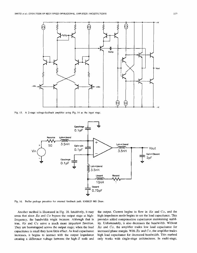
To evaluate the relative performance of a dedicated buffer,
three examples of typical 800 MHz unity-gain buffers are
compared. If the feedback was connected outside the package,
a simplified total parasitic load model for a standard 8-pin
SOIC (Small Outline Integrated Circuit) style package might
look like Fig. 16. Fig. 17 shows a simulation illustrating thethree cases. Case 17(a) is the bandwidth plot where there are no
parasitic; case 17(b) is the bandwidth plot when the feedback
is connected outside the package, on the circuit board; and case
17(c) is the bandwidth plot with the feedback closed on-chip.
Although case 17(c) shows some peaking in the closed-loop
response, it is clearly a great improvement over case 17(b).
The remaining instability or peaking shown in case 17(b)
comes from the capacitive load which at 2 pF is still very
light. There are several ways to improve this situation. The
first way is to include a series resistance at the output to isolate
the capacitive load from the amplifier. Of course this means
that our amplifier no longer has low output resistance which
for many applications is a serious disadvantage.
SMITH et d : EVOLUTION OF HIGH-SPEED OPERATIONAL AMPLIFIER ARCHITECTURES 1171
–Vin
Fig. 15. A 2-stage voltage-feedback amplifier using Fig. 14 as the input stage.
O,lpF T
Vin
Rsource Lpin+Lbond
+
‘“ & Lpin+Lbond
3.5nH
Lboord Rboard
10nH 1
Cboord
T
0.75pF
Fig. 16. Buffer package parasitic for external feedback path. EMBED MS Draw.
Another method is illustrated in Fig. 18. Intuitively, it may
seem that since Rx and Cz bypass the output stage at high-
frequency, the bandwidth might increase. Although that is
true, Rx and Cx serve a much more important function.
They are bootstrapped across the output stage; when the load
capacitance is small they have little effect. As load capacitance
increases, it begins to interact with the output impedance
creating a difference voltage between the high-Z node and
the output. Current begins to flow in Rx and Cx, and the
high-impedance mode begins to see the load capacitance. This
provides added compensation capacitance maintaining stabil-
ity. Unfortunately, it also decreases the bandwidth. Without
Rx and Cx, the amplifier trades low load capacitance for
increased phase margin. With Rx and Cx, the amplifier trades
high load capacitance for decreased bandwidth. This method
only works with single-stage architectures. In multi-stage,

1172 IEEE JOURNAL OF SOLID-STATE CIRCUITS, VOL. 29, NO. 10, OCTOBER 1994
W(J MHz Butter - Package Mras]tlc Interaction
‘“~
Fig. 17. A simulation illustrating the effect of 8-pin SOIC package parasiticon an otherwise ideal 800 MHz buffer.
ELT+”High–Z
Node Rx CX
“out
T_ c’
–v
Fig. 18. Bootstrap capacitive load compensation.
integrator type compensations schemes, the inclusion of Rx
and Cx could make the stability worse.
A final method that is available to a unity-gain-only am-
plifier is to provide an open-loop output as shown in Fig. 19.
In this case, not only is the feedback connected on-chip, but
the output capacitance is isolated from the feedback point
by the beta of the drive transistors. The output resistance
is not reduced by the loop gain any longer, although it isset by the bias current in the drive transistors and can be
arbitrarily low. Also, the bandwidth is not a direct function
of the load capacitance. Finally, the feedback loop keeps the
offset relatively low.
V. DISTORTION IN BIPOLAR AMPLIFIERS
Harmonic and intermodulation distortion in amplifiers has
always been a concern to analog designers. Perhaps the best
approach to low-distortion design is to address each distor-
tion source separately. Also, despite the apparent differences,
the distortion mechanisms in voltage and current-feedback
amplifiers are surprisingly similar.
“n*1
Vout
TCL
–vI I
Fig, 19. Open-loop output isolation.
+V
*
+
VBE+vin “out
IER’
I +–v
Fig. 20. A simple class-A output stage.
First, consider the output stage. Class-A output stages
(Fig. 20) do cause distortion despite some pseudo-science to
the contrary, and the harmonics produced are both odd and
even. Ignoring beta nonlinearity, then the equations for second
and third harmonic distortion are, respectively:
HD2 =vin . VT
[
(3)4.1 E2. RL2. l+*+ 4:!$::3+& 1
HD3 =vin2 . VT
[ 1(4)
12. IE3 . RL3 1 + ~ + ~~$:~, + & .
Each harmonic is at least a function of the input voltage
(win), the load resistance (RL), and the implied nominal
power dissipation (Ill). In fact, this is true of most distortion
mechanisms. In most designs, the peak input voltage and
load resistance are fixed, so as the quiescent current linearly
decreases, the distortion exponentially increases.In a high-bias class-A13 stage, some of the even harmonics
will cancel. The governing equation can be shown to be:
HD2 =4. (Ap – An)
3.7r. (Ap+A?z)(5)
where Ap and An are the positive and negative going gains
respectively, Therefore, to the extent that the positive and neg-
ative paths match in both gain and phase, the even harmonics
are zero. Although there may be odd harmonics that remain,
there can easily be a net decrease in harmonic distortion. To
illustrate the importance of gain and phase matching, consider
the possible output stages shown in Fig. 21. The simulation
results for a 1.0 Vpk, 20 MHz input are given in Fig. 22.

SMITH et al.: EVOLUTION OF HIGH-SPEED OPERATIONAL AMPLIFIER ARCHITECTURES 1173
HD2 %‘in”T” (:::’::::) “c’’” f”/ l+(z~ (:::’;:::) ctof)’
(8)
~(l+~~(:::’~:::t)c’of)z)’
m+5
1ma
Q1
20XQ320X
Vdc
I:!!, ,!,!
:,,,:, !
x’ l---v,$$--!’+) +Rload
Wn Q4 10020X
+cITiQ2 ~
20X
1ma
–5 Vdc
OuqxrtStage~ompmson
2ndH&-mom. 3rdH-..
I IIt .—F,,2, b
1m”rT+5vdcFig. 22. Distortion simulation of the two output stages.
aQ3 Q120X 20X
capacitance is [14].
Cj
T
Vout C(VIN + vin) =+
[ 1MJ “
Vin Q4 Q2 Rload ~ _ VINv~vin
20X 20X 100
-+
4c_._l&
1ma
–5 Vdc
Fig, 21. A comparison of 2 traditional class AE) output stages.
Even when the devices are the same size with similar bias
current, the distortion of the circuit shown in Fig. 21(a) is
much lower. In- particular, since the positive and negative
~ going paths contain both an n-p-n and a p-n-p, the evenharmonics almost cancel.
The near doubling of the third harmonic in circuit 22(b)
over 22(a) is caused by the additional parasitic substrate
capacitance from the diode-connected transistors. The signal
current required to charge that capacitance is drawn from the
input and must pass through the diodes. As the diodes are
modulated, they generate odd harmonics. They also generateeven harmonics which are rejected according to the previous
argument.
Another common source of distortion is nonlinear junction
capacitance. Although junction capacitance is at its highest
in the forward active region, the bias voltage is reasonably
constant. Hence, reversed-biased junctions are usually a big-
ger source of error. The general equation for this junction
(6)
Now consider the case illustrated in Fig. 23 where a linear
resistor is driving a reversed biased junction capacitance. The
second harmonic tends to dominate. Using Volterra series
expansion, a simplified formula can be shown to be:
HD2 Nvin. m. RS. cl. .f” /1+(2 .7r. RS. CO”.f)2 ~7)
/(1+( 4.7r RSCO”f )2)3
where:
CJ . MJq =
co= [aMJ (l+MJ) “
VjVj. [1–~ 1
This same equation applies to a dominant source of distortion
in a single-stage operational amplifier. Take, for example, the
folded-cascode (Fig. 10). A large portion of the distortion
in those architectures comes from the high-impedance node
driving the nonlinear junction capacitance connected to it. Forthis case, the open-loop distortion is approximately [see (8)
top of this page], where:
ctO = cjcOp + cjcOn + cjsOp + cjson
ctl = cjclp – cjcln + cjslp + cjsln
and rent and roPt are the general output impedances loo~ng
toward the n-p-n and p-n-p respectively on the high impedance
node.

1174 IEEE JOURNAL OF SOLID-STATE CIRCUITS, VOL. 29, NO. 10, OCTOBER 1994
r--’%-”””’b+
Vin=VIN+vin1T
C(VIN+vin)
Fig. 23. A simple junction capacitance distortion example.
+5 Vcic +5 Vdc
iclJ J’
ic2
+
vci/2 Vd/2
1ma
–5LVdc –5LVdc
(a)
+5 “dc +5 “dc
1 maL j,icl
Q3 ] QI
Rdgen
+
Vd/2 Vd/2
A ILic2
1 ma
YI–5 “dc –5 “dc
(b)
Fig. 24. (a) Voltage-feedback input stage. (b) Current-feedback input stage.
If the n-p-n and p-n-p base-collector and the collector-
substrate capacitances match, the even harmonics tend to zero.
They almost never do match, but in some cases additional
nonlinear capacitance may be added to the n-p-n to improve
the matching and lower distortion.
The last source of distortion considered here is the input-
stage which supplies the small signal (or not-so-small sig-
nal) charging current to the compensation capacitors, To
compare the differences between input-stage topologies at
high frequencies, consider Fig. 24. These are voltage-feedback
and current-feedback input-stages respectively, having similar
power dissipation and transconductance. Only the input-stage
need be considered since the rest of the amplifiers can be
made identical if necessary.
Voltage keedback - Current Yeedback Comparison
‘“”~
Fig. 25. Voltage-feedback-current-feedback input stage distortion compari-son simulation.
Suppose, for example, that the input signal is 1.0 Vpk at 20
MHz. Suppose that the rest of the amplifier provides 20 dB
(10 V/V) of loop gain at that frequency which approximately
corresponds to a 300 MHz amplifier. That implies that the
magnitude of the input voltage Vd = 1 Vpk/( 10 VN), or
Vd = 0.1 Vpk. Fig. 25 illustrates the results for a typical
high-speed process.
At this frequency, the second harmonic is comparable for
both circuit input-stages and, at least with a voltage-feedback
amplifier, could be eliminated by differential rejection. With
the third harmonic, the current-feedback amplifier is superior.
To improve the third harmonic for the voltage-feedback am-
plifier, an exotic technique like feed-forward error correction
or an increase in power would be required.
VI. SINGLE-CHIP BASE ARRAY USED
TO FABRICATE FOUR AMPLIFIERS
With this background in mind, a unique array of components
has been fabricated on a common base chip. Consisting
of transistors, resistors, and capacitors, the base array was
used to produce a family of four state-of-the-art operational
amplifiers with highly different characteristics. This approach
was selected to maximize productivity of the design effort
and to reduce development costs. This methodology requiredidentifying the common elements in each device’s architecture
while adding the minimum of additional circuitry to form four
distinct architectures.
Each amplifier is optimized in some important area such
as bandwidth, distortion, slew rate, and power dissipation. An
operational amplifier can be represented in block diagram form
by the major elements shown in Fig. 26. Each architecture uses
all of these blocks as a way to share their common elements,
but the blocks are tailored to the requirements of the individual
amplifiers. Table I shows the contrast between the important
specifications of each amplifier architecture.
A decision was made during the early phases of the project
to choose a process that would enable the products to be
distinguished on the basis of performance. Another compelling

SMITH et al.: EVOLUTION OF HIGH-SPEED OPERATIONAL AMPLIFIER ARCHITECTURES 1175
Intermediate
Input Stage Gain StageOutout Staae
Fig. 26. Operational amplifier block diagram.
TABLE ISUMMARY OF AMPLIFIER SPECIFICATIONS
I I W@ebar,d I Low-dslotion I c!lrmt-fccdba& I Iaw-pwel-36S Bmdwd!h
SL=lcm n 13GH2 4SOMHZ 1 GRz 650 MRZ
CL=5PF
Voltqm Nom 29 nV/4Hz 23 nV/iHz 40 nV/4Hz 7 I nV/i3kz
Settling Tune 18 IIS Ilsns 8 .s 115ns
(o l%)
slew Irate 350Vlws 380V/IIS
2c@ WI18 180Wp,
Ad $7da 95lm 250m 55dB
DISkmIOU&5MH2v,” = Ivp
RL=ioon 856s. 95 m. 706W 826S,
(W= 500 C2)
55 mw
TABLE II
SUMMARY OF TYPICAL 6X SIZE TRANSISTOR
SPECIFICATIONS FOR THE AT&T CBIC V2 PROCESS
II Parameter NPN I PNP
Hfe 118 45 —
Ft 10.2 43 GHr.
Va 27 11 volts
BVCEX 12 15 volts
CJC 0.079 0.199 PF
CJS 0102 0.593 PF
Rb 52.8 401 Olrnls
reason to emphasize performance was to offset the fact that
die size is not optimum due to the need to accommodate four
different designs at one time. The AT&T CBIC-V2 process
was chosen to achieve the desired performance. Table II shows
a summary of the important features of this process.
VII. DIFFERENTIAL AMPLIFIER ARCHITECTURES
Fig. 27 through Fig. 30 show simplified schematics of the
four differential operational structures that have been im-
plemented. The widest bandwidth architecture is the folded-
cascode and is shown in Fig. 27. Being a single-stage ampli-
fier, the dominant pole formed by output impedance of the
gain stage and the compensation capacitor. Since there are a
fewer secondary poles to deteriorate the phase margin than in
a typical multi-stage amplifier, the bandwidth is maximized.
\J...,
Fig. 27. Folded cascode architecture,
Ut
Vee
Fig. 28. Low-distortion architecture.
Fig. 28 shows a simplified schematic of the low-distortion
amplifier; it has the highest open-loop gain and achieves lowest
offset due to its balanced nature. Low, high-frequency distor-
tion is achieved via a double integrator feedback loop applied
around the second gain stage, thereby reducing the second-
stage and output stage distortion mechanisms to second-order.
The amplifier illustrated in Fig. 29 is a current-feedback
arrangement which achieves the highest slew rate of the
different configurations. This current-feedback amplifier has
the property that bandwidth is normally independent of the
gain, unlike voltage-feedback amplifiers where the bandwidth
varies with the gain setting.
The low-power amplifier shown in Fig. 30 also uses the
folded-cascode architecture, and even though the power dis-
sipation is about a third of the higher power version, the
bandwidth is only cut in half. This amplifier has the poorest
noise performance as a consequence of reduced bias current.
It is a well-known fact that proper and adequate power
supply capacitive bypassing is essential to the stability of
an operational amplifier. Parasitic supply inductance has a
tendency to provide a positive internal feedback path which at
best will decrease the phase-margin and at worst will cause

1176 IEEE JOURNAL OF SOLID-STATECIRCUITS, VOL. 29, NO, 10. OCTOBER 1994
Vcc
RI R2 n.
+Vin {- ‘4 -Vin Icll
-t-
221
220Vout
.
‘“y’ ‘flQ18q’~Vee
Fig. 29. Current feedback architecture.
R4 R5BiasLine
#—
Q4k Q5~
RI Q6
R3
Vee
%5
YQ15
~ne Q13
Q12 QI 6Q20
cc+
M
Vout
Q11 , Q19
1 Q1O$ I
Fig. 30. Low-power Urchltecture,
oscillations. As the unity-gain bandwidth of the amplifier
increases, the tolerance of the amplifier to power supply
parasitic inductance decreases. Hence, one of the special
features of these amplifiers is the inclusion of 50 pF of on-
chip bypass capacitance. Although a substantial penalty in die
area was paid, it ultimately allowed the standard operational
amplifier 8-pin packages and pin-outs to provide bandwidth in
excess of 1 GHz.
VIII. INPUT AND GAIN STAGE
A. Wideband Ampl&er
The folded-cascode amplifier, Fig. 27, shows the input
applied to the differential input-stage formed by Q1 and Q2.
Emitter resistors R1 and R2 improve the slew rate by allowing
the compensation capacitor to be smaller. Collectors of Q1
and Q2 are connected to the emitters of the p-n-p transistors
Q4 and Q5 as the signal is directed or “folded” towards the
negative bias rail. This arrangement enables a simple single-
stage amplifier to have a high common-mode input range as
well as a large signal swing at the output. Other architectures
achieve similar input and output signal swings, but usually
two stages.
The collectors of Q4 and Q5 are connected to a Wilson
current mirror composed of transistors Q6, Q7, and Q8 to
increase the output impedance and gain of this stage. R6 and
R7 stabilize the current mirror. Capacitor Cc along with the
output impedance at the node formed by the collectors of
Q5 and Q6 form the dominant open-loop pole. The unity-
gain crossover frequency is approximately determined by the
(RI + R2) . Cc time constant:
Unity Gain Bandwidth x1
2.7r. (Rl+R2). cc(9)
The extrinsic degeneration resistors RI + R2 are usually
greater than the intrinsic emitter resistance re.
B. Low-Distortion
Fig. 28 shows the schematic of a low-distortion vokage-
feedback amplifier that uses two gain stages to increase
open-loop gain and places a feedback loop around the final
high impedance node and output stage to reduce distortion.
Transistors Q3 and Q4 form the input differential amplifier
with emitter resistors R3 and R4. Q 1 and Q2 serve as the
collector load current sources for this stage. Bias for the input
is provided by current source Q5 with emitter transistor R5
setting the value of the current. Emitter follower Q7 and Q 16
buffer the output of the input before its signal is applied to the
second gain stage. Bias for these emitter followers is set by
current sources Q6 and Q 15 with R1O and R12 establishing
the value of the current.
Common-mode feedback from the second-stage is applied
to the bases of Q 1 and Q2 so that the current from these
current sources exactly matches the current through Q4 and
Q4. The signals at emitters Q7 and Q16 are then applied to
the bases of Q!3 and Q 10 which is the input pair of the second
gain stage. The signal from the collector of Q9 and Q1O are
loaded by a Wilson-type current source to increase the gain
of this stage.
The Wilson current sources consists of transistors Q1l-Q14
along with resistors R6 and R7. Balanced feedback is applied
around the second-stage and output buffer, by capacitors Cl
and C2 forming a differential mode integrator. R8, R9, and
Cc serve to stabilize the frequency response of the this stageas it is a feedback amplifier in its own right. The unity-gain
crossover frequency is calculated as follows:
Unity Grain Bandwidth =1
2.n. (R3+R4). (Clor C2)”
(lo)
Bias for the second-stage is provided by the current source Q8
with R11 setting the value of the current. The output of the
second-stage is taken from the common collector connection
of transistors Q 10 and Q 14, and it is applied to the output
stage to form the entire amplifier. Different versions of this
architecture are created by lowering the values of R3 and R4for requirements where the allowable closed-loop gain may be
higher than unity. The high-gain versions are lower in noise
because the values of R3 and R4 are lower.

SMITH etal. EVOLUTION OF HIGH-SPEED OPERATIONAL AMPLIFIER ARCHITECTURES 1177
C. Current-Feedback
The current-feedback architecture (Fig. 29) has the poorest
offset and drift performance compared to the other amplifiers
due to the non-symmetrical input-stage. The differential signal
is applied to the common-emitter connection of the Q3 and Q5
and the Q4 and Q6 pairs. Bias for the input-stage is applied
from the biasing block to the bias lines connected to the bases
of Q 1 and Q7. Resistors Ill and R3 determine the value of
the quiescent current for the input-stage. The current that flows
through Q3 and Q5 provides the base bias voltage for the Q4
and Q6 pair.
During transient operation the current-feedback amplifier
draws current from the power supplies providing more current
for slewing the compensation and parasitic capacitance. Under
zero-signal condition, the current flow through the input-stage
is reflected through the branch containing Q 10 and Q 11 by
the action of Wilson mirrors Q2, Qll, Q12 and Q8, Q9, Q1O.
During dynamic conditions the additional current that passes
through the input-stage then becomes available to the output
stage for purposes of charging the compensation capacitance
cl.
The input signal current that appears on the emitters of Q4
and Q6 passes through their collectors and is then applied to
the previously described Wilson current sources to amplify the
signal. R2, R4, R5, and R6 provide emitter degeneration for
the current sources to stabilize their operation. The unity-gain
crossover frequency is given by:
Unity Gain Bandwidth %1
2.7r Rfb. C’1”(11)
Not shown in the Fig. 29 schematic is the feedback resistor
Rfb connected between the output and –Vin. The common-
collector connection of Q1O and Q 11 is buffered by an output
stage formed by transistors Q13 through Q24 and resistors
R7 through R9.
D. Low-Power
The low-power amplifier architecture shown in Fig. 30
is also a folded-cascode architecture, similar to that of the
wideband version. Because of the Darlington style output
stage, it was not necessary to use the extra emitter follower
used for the wideband amplifier. A bandwidth of 650 MHz
is achieved in spite of the power dissipation being reduced
by a factor of three. Exceptionally wide bandwidths can be
achieved at low current levels, but at the expense of poorer
noise performance and slew rate. Examination of (9) shows
that the tradeoff can be made between the emitter degeneration
resistors R1 + R2 and the compensation capacitor Cc and
maintain the same unity-gain bandwidth. Slew rate is given
by:
Slew Rate =.& (12)
where I is current flowing through the current source Q3.
High slew rate also can be maintained at low power levels
by setting the value of Cc low which would correspond to
a compatible low value of 1. However, once that has been
set, the value of the emitter degeneration R1 + R2 must be
Vee
Fig. 31. Typical output stage.
Vcc
RIBias
Virto
Bias
R2
‘1-1-w’
Fig. 32. Low-power output stage,
increased to maintain the desired unity-gain bandwidth which
then increases the noise level. This can be seen by:
(13)
where en is the resistor noise level, k is Boltzman’s constant,
T is temperature, B is noise bandwidth, and R is resistance.
IX. OUTPUT STAGES
Fig. 31 and Fig. 32 show the schematics of the output stages
used for the differential amplifiers. The schematic in Fig. 31 is
used for all of the amplifiers except for the low-power version.
Both output stages are biased in the AB region at a high
enough level to eliminate crossover distortion.

1178 IEEE JOURNAL OF SOLID-STATE CIRCUITS. VOL. 29, NO 10, OCTOBER 1994
Vcc
Q7
R6
%
Bias
Line
Q6
1
Vee
Fig. 33. Amplifier biasing circuit.
For the typical output stage, the signal is applied to the
common bases Q3 and Q4. The output of these emitter
followers is then sent to the bases of the output transistors Q8
and Q9. Bias for Q3 is developed through current source Q2.The value of the bias current is determined by the Vbe of Q 1
being applied across R2. In a similar manner, the bias current
for Q5 is established through the action of Q5, Q6, and R3.
Transistor pairs Q7-Q11 and Q1O-Q12 guarantee adequate
output current drive due even for the worst case low beta
that could occur due to process and temperature extremes.
Load current flowing through either Q8 or Q9 is reflected
through the current mirror action of Q7 or Q1O so that an
increase in output current is conducted through Q 11 or Q 12
depending upon the polarity of the signal. The total quiescent
current drain for this output buffer is 7 mA and is capable
of supplying 50 mA into a 50-fl load. The bandwidth of this
output stage is in excess of 5 GHz which is wide enough not
to cause phase-margin difficulties.
The output stage shown in Fig. 32 was designed to be
the buffer for the low-power amplifier, drawing just 3.1 mA.
The entire current drain for the low-power amplifier is only
5.5 mA. The input signal is applied to the bases of Q3
and Q4. The positive going signal is level shifted by Q5
before being applied to the base of Q1O. The emitter of Q 10then driven by the p-n-p emitter follower Q 12. Bias for this
group of transistors is established by current source Q6. R2
attached to the emitter of Q6 determines the value of the bias
current. The node labeled Bias Line is connected to the bias
circuitry associated with the rest of the amplifier. Negative-
going signals are processed in an analogous manner through
Q3, Q2, Q7, and the output n-p-n emitter follower Qll,
Q1 and R1 establish the bias for the previously mentioned
transistors. The compound connection of Q8 and Q9 are used
to bias the output stage Q11 and Q12.
X. BIASING
The biasing circuitry is shown in Fig. 33. The current
that flows through the circuit defined by Q2 through Q5
and resistors R2 through R4 form a PTAT (Proportional To
Absolute Temperature) floating current source. The value of
the current that flows through this current source is:
[1A2 . A5l=~ln —
A3 . A4
where 1 is the value of the current, VT’ istemperature, R = R3 = R4 and A2, A3,
(14)
26 mV at room
A4, and A5 are
the relative area of transistors Q2 through Q5 respectively. If
one assumes that all the Vbe voltages are about the same, the
current in Q7 is approximately:
VbeIE—
R6 “(15)
Since the current given by (14) increases with temperature
and the current given by (15) decreases with temperature, it
is possible to sum these two currents to create a combined
current that is approximately independent of the temperature.
Additionally, this combined current source has a high degree
of power supply independence which is ideal for biasing
an operational amplifier. Also, (14) and (15) indicate, to
the first order, that power supply does not effect the bias
current at all. Those equations neglect the output impedance
of the transistors, which is responsible for some power-supply
dependence.
Schematics of the previously described amplifiers make
reference to connections labeled bias line. Transistor Q 1 and
resistor RI form a biasing rail that is used to bias the current
sources attached to the positive power supply or various parts
of the amplifier. Q6 and R5 perform the same function for
circuits attached to the negative power supply in various parts
of the amplifier.
XI. CONCLUSION
“Never throw anything away” is the phrase that best de-
scribes the evolutionary development of operational amplifiers.
Going back to circuits developed nearly a half century ago,
today’s operational amplifier designer has a vast supply of
circuits to draw from in implementing new designs. This article
has traced the evolution to a real design application that made
use of many of the circuits and techniques developed over
time. The net result is not only time saving for the designer, but
reduced cost for the development of state-of-the art operational
amplifiers using the most sophisticated processing technology
available.

SMITH d al.: EVOLUTION OF HIGH-SPEED OPERATIONAL AMPLIFIER ARCHITECTURES 1179
[1]
[2]
[3]
[4]
[5]
[6]
[7][8]
[9]
[10][11][12][13][14]
REFERENCES
AT&T Microelectronics CBIC-V Product Development Guide, FkstEdition, April 1993.J. R. Razazzini. R. H. Randall. and F. A. Russell. “Analvsis of moblems. .in dyna;ics by electronic circuits,” in Proc. I. R. E., May 1947.C. Davis, G. Bajor, J. Butler, T. Crandell, J. Delado, T. Jung, Y. Khajeh-Noori, B. Lomenick, V. Miliam, H. Nicolay, S. Richmond and T. Rivoli,“UHF-1: A high speed complementary bipolar process on SOI,” BCiWf92 Dig. of Tech. Papers, Oct. 1992.Members of the Staff of the Department of Electrical Engineering ofthe Massachusetts Institute of Technology, Appl. Electron., New YorkWiley, p. 531, 1943.D. R. Breuer, “Some techniques for precision monolithic circuits appliedto an instrumentation amplifier,” IEEE J. Solid-State Circuits, vol. 3,no. 4, Dec. 1969.H. R. Eckes, “Design, test, and application of high speed integrativedifferential analyzer,” Ph.D. dissertation, University of Arizona, Tucson,1967.U.S. Patent 3,852,678, Dec. 3, 1974.P. R. Gray and R. G. Meyer, Analysis and Design of Analog Integrated
Circuits Third Ed., New York Wiley, 1993, p. 283.D. Nelson, “OP AMPS for wideband, fast settling applications,”WESCONConfi Record, p. 15/4, Nov. 1986.R. Gosser, Private Communication, July 1, 1993.U.S. Patent 4,970,470, Nov. 13, 1990.AD9617 Data Sheet, Analog Devices, Norwood, MA.U.S. Patent 5,003,269, March 29, 1991.P. Antognetti and G. Masobrio, Semiconductor Device Modeling with
SPICE. New York McGraw-Hill, 1988, P. 27.
Douglas Lee Smith received the B.S.E.E. from theUniversity of Arizona, Tucson, in 1988.
In 1988 and 1989, he worked as a test engi-neer for Analog Devices, Inc., in Greensboro, NC.From 1989to 1994, heworked forthe B~-BrownCorporation, Tucson, AZ, where most recently hedesigned the 0PA64X family of high-speed op-erational amplifiers. In July 1994, he left Burr-Brown Corporation to form the Gain TechnologyCorporation, ananalog andrnixed-signal IC designcommmv in Tucson. In addition, he is completing
Mike Keen was born in Brooklyn, NY, in 1939.He received the B. S.E.E. and M. S.E.E. degree fromNew York University, New York, in 1960 and 1964,respectively.
Since 1977, hehasbeen working at Brsrr-BrownCorporation, Tucson, AZ, as a design manager spe-cializing in the design of high-speed digital toanalog converters, analog to digital converters, andoperational amplifiers. Hehassix patents relating totopics in these areas.
Mr. Koenisa member of Eta Kappa Nu.
Arthur F. W]tulski received the B.S., M. S., andPh.D. degrees in electrical engineering from theUniversity of Colorado, Boulder, in 1981, 1986, and1988, respectively.
From 1981 to 1983, he worked as a power supplydesign engineer at Storage Technology Corpora-tion, Louisville, CO. Since 1989, he has been anAssistant Professor at the University of Arizona,Tucson, where he teaches classes in analog, digital,and power electronics. His research interests are inmodeling and design of switching power converters
and analog electronic circuits. -
. .the M. S.E.E. degree at the University of Arizona, where his research ”area;the analysis and design of low-distortion amplifiers.