Embed Size (px)
Citation preview
RSC Advances
PAPER
Publ
ishe
d on
28
July
201
5. D
ownl
oade
d by
Bilk
ent U
nive
rsity
on
08/0
1/20
16 1
7:10
:01.
View Article OnlineView Journal | View Issue
Excitation depen
aUNAM-National Nanotechnology Research C
Turkey. E-mail: [email protected];
bilkent.edu.trbInstitute of Materials Science & Nanotechn
Turkey
† Electronic supplementary informa10.1039/c5ra09787h
Cite this: RSC Adv., 2015, 5, 66367
Received 25th May 2015Accepted 28th July 2015
DOI: 10.1039/c5ra09787h
www.rsc.org/advances
This journal is © The Royal Society of C
dent recombination studies onSnO2/TiO2 electrospun nanofibers†
Veluru Jagadeesh babu,*a Sesha Vempati,*a Yelda Ertasab and Tamer Uyar*ab
Poly(vinyl acetate) (PVAc)/TiO2 nanofibers, PVAc/SnO2 nanoribbons and PVAc/SnO2–TiO2 nanoribbons
were produced via electrospinning. TiO2 nanofibers and SnO2 nanoribbons were obtained by removal of
the polymeric matrix (PVAc) after calcination at 450 �C. Interestingly, PVAc/SnO2–TiO2 nanoribbons
were transformed into SnO2–TiO2 nanofibers after calcination under the similar conditions. Fiber
morphology and elemental mapping confirmed through SEM and TEM microscope techniques
respectively. The X-ray diffraction measurements suggested the presence of anatase TiO2 and rutile
SnO2 and both were present in the SnO2–TiO2 mixed system. Systematic photoluminescence studies
were performed on the electrospun nanostructures at different excitation wavelengths (lex1 ¼ 325,
lex2 ¼ 330, lex3 ¼ 350, lex4 ¼ 397 and lex5 ¼ 540 nm). We emphasize that the defects in the SnO2–TiO2
based on the defect levels present in TiO2 and SnO2 and anticipate that these defect levels may have
great potential in understanding and characterizing various semiconducting nanostructures.
Introduction
1D nanostructures via electrospinning have attracted signi-cant attention due to the fact that their distinctive surface andquantum effects can inuence the functionality and perfor-mance in nanodevices.1–5 Among semiconductors, SnO2 andTiO2 have evoked considerable attention due to their potentialapplications in optoelectronic devices,6–8 despite the anatasephase of TiO2 being more photoactive.9 It has been found that acombination of SnO2 and TiO2 gives the most signicantsensing and photocatalytic applications.10,11 In addition, SnO2
and TiO2 have a large bandgap (3.2 eV for anatase TiO2 and 3.6eV for SnO2)12,13 which ensures that the electrons within theconduction band (CB) have a strong reducing ability and theholes in the valence band (VB) have a strong oxidizing ability.14
The impurities or defect states induced by the synthesismethods can form deep energy levels (which act as trappingcentres) or shallow energy levels (which act as donors).15 Theseshallow trap levels (lying in the bandgap) act as carrier traps incompetition with the fast carrier recombination in the bulkduring photoexcitation, which enhances the photoactivity of thenanostructures. On the other hand, Zhu et al.16 reported that byconsidering chemical potentials, the deep trap levels exhibitedreduced photocatalytic activities. Titania is a highly ionic
entre, Bilkent University, Ankara, 06800,
[email protected]; uyar@unam.
ology, Bilkent University, Ankara, 06800,
tion (ESI) available. See DOI:
hemistry 2015
lattice17 with a VB composed of oxygen 2p orbitals (the wavefunctions are considerably localized on the O2� lattice site),while the CB consists mostly of excited states of Ti4+. The widthof the VB in O2� 2p is about 16 eV and the breadth of the CB inTi4+ 3d is about 27 eV.18
Optical spectroscopy studies have been used extensively forthe detection of CB electrons, trapped electrons, holes, andtransition energy levels. Ghosh et al.14 reported that the rutileTiO2 single crystal consists of at least eight shallow trap levels(<1 eV below the CB). Later, the midgap energy related defectswere identied from surface or bulk trap state luminescenceeither by surface modication of TiO2 nanoparticles with aloading of platinum19 or by treatment with TiCl4.20 Ariga et al.21
demonstrated that photo-oxidation on the TiO2 (001) surfacehas a threshold energy between 2.1 and 2.3 eV (539–590 nm),which is apparently much lower than that of the bandgapenergy (3.0–3.2 eV). The two defect related bands were observedin titanate nanostructures (at 463 and 533 nm)22 and assigned tocarrier trapping at defect centers. On the other hand, the opticalproperties of SnO2 are of great importance because of the evenparity symmetry which precludes from the band-edge radiationtransition.23 Upon reducing the dimensionality of the SnO2
crystals, the wave function symmetry can be broken due toquantum connement and hence the dipole forbidden selec-tion rule can be relieved, giving rise to the free exciton emis-sion.24 The luminescence would be dependent on the shape ofthe nanostructures such as the shbone-like nanoribbons ofSnO2 that exhibit green emission.25 Luo et al.26 performedtemperature dependent PL on SnO2 nanowires and nanobeltswhere two bands centered at 470 nm and 560 nm were observedwith the intensity of the former band being strongly dependent
RSC Adv., 2015, 5, 66367–66375 | 66367
RSC Advances Paper
Publ
ishe
d on
28
July
201
5. D
ownl
oade
d by
Bilk
ent U
nive
rsity
on
08/0
1/20
16 1
7:10
:01.
View Article Online
on temperature. Blue/violet emission was also reported fordifferent shapes of SnO2 nanocauliowers, nanoblades, andother types of nanostructures.27–30 Kar et al.31 reported themorphology dependent luminescence for SnO2 nanorods andnanoparticles. The exciton binding energy of SnO2 is as large as130 meV, which envisages efficient exciton emission at roomtemperature and even at higher temperatures. Kılıç andZunger32 observed ve intrinsic defects coexisting in SnO2,which are oxygen vacancies (VO), tin vacancies (VSn), tin antisitedefects (SnO), oxygen interstitial sites (Oi) and tin interstitialsites (Sni). Sni and VO are the predominant defect structures inSnO2 due to the multivalency of tin. These defect structures canproduce shallow donor levels that cause n-type conductionwhich originates from the VO, where the VO can capture elec-trons which leads to singly ionized vacancies (VO
+) or doublyionized vacancies (VO
++). However, there are inadequate reportson electrospun SnO2/TiO2 nanobers with excitation dependentemission spectra analysis.
In the present study, the systematic excitation dependentphotoluminescence (PL) on TiO2, SnO2 and SnO2–TiO2 electro-spun nanobers are conducted. The PL emission peaks aredependent on the bandgap and surface defects. The plausibleband alignment is also proposed and discussed with respect tothe excitation energy.
ExperimentalMaterials
All the chemicals were purchased and used without furtherpurication: titanium(IV) isopropoxide (TIP, 97%, Sigma-Aldrich); tin(IV) chloride (SnCl4, 99%, Sigma-Aldrich); poly(-vinyl acetate) (Mw: 350 000); methanol (99%, Sigma-Aldrich);and glacial acetic acid (100%, Merck).
Synthesis of the nanostructures
The preparation of nanostructures via electrospinning is a well-known technology.33,34 The polymer solutions were prepared bydissolving 1.2 g of PVAc in 10 mL of methanol and stirring for�3 h. For the TiO2 preparation, 2 mL of glacial acetic acid wasadded to the polymer solution, followed by 1 mL TIP which wasthen subjected to stirring for �6 h to obtain a clear andhomogeneous solution. For the SnO2 synthesis, 0.5 mL of SnCl4was added to the polymer solution (PVAc) and subjected tostirring for �6 h. Whereas for the SnO2–TiO2 solution, 2 mL ofglacial acetic acid, 1 mL TIP and 0.5 mL of SnCl4 were added tothe polymer solution (PVAc) and subjected to �6 h of stirring.
The solution was taken in a 10 mL syringe (21 G 1/2 needle)and was placed in a commercially available electrospinningmachine Nanoweb (Electrospin 100) for the preparation of thenanobers. The ow rate was adjusted to 25 mL m�1 with asyringe pump (KD Scientic, KDS 101), the distance between thetwo electrodes (tip of the needle to collector) was maintained at8 cm, and the applied voltage between the rotating drumcollector (with a speed of 200 rpm) and the tip of the needle was15 kV. The electrospun PVAc/TiO2 nanobers, PVAc/SnO2
nanoribbons and PVAc/SnO2–TiO2 nanoribbons were then
66368 | RSC Adv., 2015, 5, 66367–66375
subjected to calcination at 450 �C for about 3 h. Aer calcina-tion the samples are referred to in a short form as TNF, SNR andSTNF, respectively.
Characterization
Thermal analysis was performed on the nanostructures using athermogravimetric analyser (TGA, Q500, TA Instruments) in therange of room temperature (TR) to 700 �C in a nitrogen atmo-sphere. The morphologies of the microstructures and nano-structures were observed by scanning electron microscopy(SEM, FEI-Quanta 200 FEG). Approximately 5 nm of Au/Pd wassputtered on the samples before they were subjected to SEMscanning. The nanobers were examined using transmissionelectron microscopy (TEM, FEI-Tecnai G2 F30). The sampleswere dispersed in ethanol and a tiny drop was dried on a holeycarbon coated TEM grid and analysed with energy dispersive X-ray spectroscopy (EDX) for elemental analysis. The crystalstructures of the nanobers were characterized using a PAN-alytical X’Pert Pro multipurpose X-ray diffractometer (XRD) inthe range of 2q ¼ 20–80� with CuKa (1.5418 A) radiation. UV-visabsorbance spectroscopy of the nanostructures was performedusing a UV-vis spectrometer (VARIAN, Cary 5000) by takingnearly 1–5 mg of dispersion in a quartz cuvette. PL measure-ments were performed on the bers as free standing akes inthe PL spectrometer (Jobin Yvon, FL-1057 TCSPC) at differentexcitation wavelengths (lex1 ¼ 325, lex2 ¼ 330, lex3 ¼ 350, lex4 ¼397 and lex5 ¼ 540 nm). The XRD peaks and PL emission peakswere deconvoluted with a Lorentz and Gauss tting respectively,with Origin 8.5 where it was necessary.
Results and discussionSurface morphology
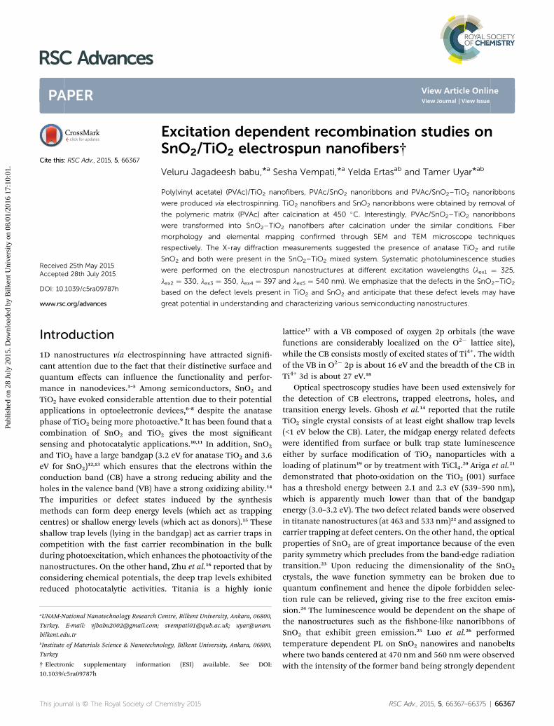
The surface morphology of the nanostructures was observed bySEM and is shown in Fig. 1. The as-spun nanostructures ofPVAc/TiO2, PVAc/SnO2, and PVAc/SnO2–TiO2 exhibit ber(Fig. 1a), ribbon (Fig. 1c) and ribbon (Fig. 1e) like structures andaer calcination they are denoted as TNF, SNR and STNF,respectively. However, all these nanostructures are smooth andbead-free. That is to say, the charges (viscoelastic force andelectrostatic repulsion) between the precursor solutions weresuccessfully balanced by controlling the process parameters(humidity, ow rate, substrate rotation speed and high voltage)to suppress the inuence of surface tension which drives thebead formation.35,36
The calcination of the as-spun nanostructures was carriedout at 450 �C. The successful removal of the polymeric part fromthe PVAc/TiO2, PVAc/SnO2 and PVAc/SnO2–TiO2 nanostructureswas rst conrmed by TGA studies. Themain weight loss occursbetween 100 and 400 �C due to the decomposition of the poly-meric matrix (PVAc) and organic content of the precursorspresent in the as-spun nanostructures (Fig. SI-1†). Interestingly,aer calcination, the morphology of TNF (Fig. 1b) and SNR(Fig. 1d) remains unchanged, whereas PVAc/SnO2–TiO2 is con-verted to ber shaped STNF (Fig. 1f) and the bers are uniformthroughout their lengths. The decrease in dimensions aer
This journal is © The Royal Society of Chemistry 2015
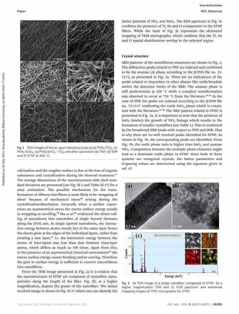
Fig. 1 SEM images of the as-spun nanostructures of (a) PVAc/TiO2, (c)PVAc/SnO2, (e) PVAc/SnO2–TiO2 and after calcination (b) TNF, (d) SNRand (f) STNF at 450 �C.
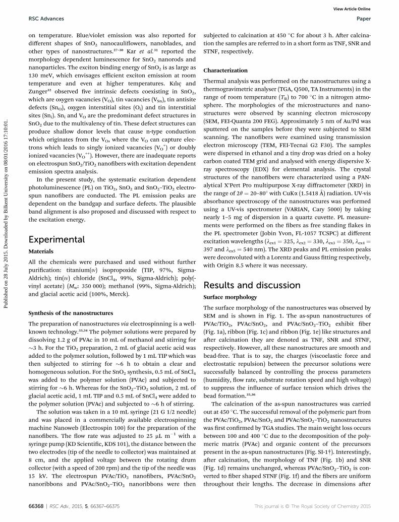
Fig. 2 (a) TEM image of a single nanofiber composed of STNF, (b) ahigher magnification TEM and (c) EDX spectrum and elementalmapping images of TEM micrographs for STNF.
Paper RSC Advances
Publ
ishe
d on
28
July
201
5. D
ownl
oade
d by
Bilk
ent U
nive
rsity
on
08/0
1/20
16 1
7:10
:01.
View Article Online
calcination and the rougher surface is due to the loss of organicsubstances and crystallization during the thermal treatment.37
The average dimensions of the nanostructures with their stan-dard deviation are presented (see Fig. SI-2 and Table SI-1†) for aclear estimation. The possible mechanism for the trans-formation of ribbons into bers is most likely to be ‘wrapping ofsheet’ because of mechanical stress38 arising during thecrystallization/dissolution. Generally when a surface experi-ences an asymmetrical stress the excess surface energy resultsin wrapping or scrolling.39 Ma et al.40 evidenced the direct roll-ing of nanosheets into nanotubes of single layered titanatesalong the (010) axis. In single layered nanosheets, the interac-tion energy between atoms mostly lies in the same layer hencethe sheets grow at the edges of the individual layers, rather thancreating a new layer,41 i.e. the interaction energy between theatoms of inter-layers was less than that between intra-layeratoms, which differs as much as 500 times. Apart from this,in the presence of an asymmetrical chemical environment39 theexcess surface energy causes bending and/or curving. Thereforethe gain in surface energy is sufficient to convert nanoribbonsinto nanobers.
From the TEM image presented in Fig. 2a it is evident thatthe nanostructures of STNF are composed of crystalline nano-particles along the length of the ber. Fig. 2b, at a highermagnication, depicts the grains of the nanober. The latticeresolved image is shown in Fig. SI-3† where one can identify the
This journal is © The Royal Society of Chemistry 2015
lattice patterns of TiO2 and SnO2. The EDX spectrum in Fig. 2cconrms the presence of Ti, Sn and O components in the STNFbers. While the inset of Fig. 2c represents the elementalmapping of TEM micrographs, which conrms that the Ti, Snand O spatial distributions overlap in the selected region.
Crystal structure
XRD patterns of the nanobrous structures are shown in Fig. 3.The diffraction peaks related to TNF are indexed and conrmedto be the anatase (A) phase according to the JCPDS le no. 21-1272, as presented in Fig. 3a. There are no indications of thepeaks related to impurities or other phases like rutile/brookitewithin the detection limits of the XRD. The anatase phase isstill predominant at 450 �C while a complete transformationwas observed to occur at 750 �C from the literature.42,43 In thecase of SNR the peaks are indexed according to the JCPDS leno. 72-1147 conrming the rutile SnO2 phase which is consis-tent with the literature.44–46 The XRD pattern related to STNF ispresented in Fig. 3a. It is important to note that the presence ofSnO2 hinders the growth of TiO2 linkage which results in theformation of smaller crystallites (see Table 1). This is conrmedby the broadened XRD peaks with respect to TNF and SNR. Thatis why there are no well resolved peaks identied for STNF. Asshown in Fig. 3b, the corresponding peaks are identied. FromFig. 3b, the rutile phase ratio is higher than SnO2 and anataseTiO2. Competition between the multiple phase elements mightlead to a dominate rutile phase in STNF. Since both of thesesystems are tetragonal crystals, the lattice parameters andd-spacing values are determined using the equation given inref. 47.
RSC Adv., 2015, 5, 66367–66375 | 66369
Fig. 3 X-ray diffraction profiles of (a) TNF, SNR and STNF and (b) STNFdecomposed using Lorentz fitting. XRD patterns are indexed accord-ing to JCPDS file no. 21-1272 and JCPDS file no. 72-1147 for anataseTiO2 and SnO2 respectively.
RSC Advances Paper
Publ
ishe
d on
28
July
201
5. D
ownl
oade
d by
Bilk
ent U
nive
rsity
on
08/0
1/20
16 1
7:10
:01.
View Article Online
From Fig. 4, the full width at half maximum (FWHM) of thediffraction peaks are obtained. The FWHM values and thecrystallite sizes (dhkl) were calculated through the Debye–
Table 1 From the XRD data of TNF, SNR and STNF, where a, b, and c, areand d is the crystallite size
Lattice parameters (A) V ¼a2 �c (A3)
Vper molecule (A3) d (nma ¼ b c c/a
TNF-A 3.7595 9.4189 2.505 133.125 33.281 11.14SNR 4.7208 3.1845 0.6745 70.967 35.484 7.50STNF-ASTNF-R 4.6288 3.0189 0.6521 64.682 32.341 3.17STNF-SnO2 4.7157 3.0999 0.6573 68.937 34.469 3.56
66370 | RSC Adv., 2015, 5, 66367–66375
Scherrer formula.48 The calculated crystallite sizes of individualTNF, SNR and STNF are presented in Table 1. The crystallitesizes of STNF are smaller than those of the individual systems.However, by changing the calcination environment to either O2
or under vacuum does not cause any inuence on the crystallinesizes.49 It is noted that at all Bragg reections assigned to thetetragonal phase, a shi to slightly higher 2q values from theSTNF system is seen. This might be due to the latticecompression/expansion during calcination. Furthermore, thesurface area (Sa) of the nanostructures is also calculated byeqn (1):50,51
Sa ¼ 6
dhkl � r(1)
where the molecular density (r) is obtained from eqn (2):
r ¼ nM
NV(2)
where n represents the number of formula units per unit cell (4for anatase and 2 for SnO2), M is the molecular weight, N isAvogadro’s number, and V is the volume of the unit cell. Thehigher the surface area is, the lower the activation energy is,which precludes the phase transformation below a certaintemperature.50
Two types of doping, viz. (a) interstitial and (b) substitu-tional, can be expected depending on the electronegativity andionic radius. For the rst one, if the electronegativity (on thePauling scale) of Sn4+ is closer to that of Ti4+ and the ionicradius (in A) of Sn4+ is smaller than that of Ti4+, then the latticespacing will become larger. Then the doping ion will enter intothe crystal cell of the oxide. While for the second one, if theelectronegativity and ionic radius of the doping metal ionsmatch those of the lattice metal ions in oxides, the dopingmetalion will substitute itself for the lattice metal ion in the dopingreactive process.52 Since the difference in electronegativity ofSn4+ (1.96) and Ti4+ (1.54) results in a change in the volume ofSTNF, it could be expected that Sn4+ will replace Ti4+ in thelattice and occupy the Ti4+ positions by substitutional doping.Therefore, the volume of the unit cell (see Table 1) of STNF ismoderately between that of TNF and SNR. In addition, the ionicradius of Sn4+ (0.71 A)53 is larger than that of the Ti4+ (0.68 A)53
ion, which will induce lattice distortions in STNF. From Table 1,the volume of the unit cell is very consistent, which indicatesthat the lattice would relax as Sn4+ ions with a larger ionic radiusare substituted for Ti4+ in TiO2.
the lattice parameters, V, is the volume of the cell, Sa is the surface area,
) Sa (m2 g�1) Peak positions
135.19214
38.687 (112) 53.560 (105)9 460.24 27.245 (110) 35.500 (101) 40.796 (111) 63.672 (301)3 231.92 34.627 (101) 55.081 (220) 66.832 (301)
This journal is © The Royal Society of Chemistry 2015
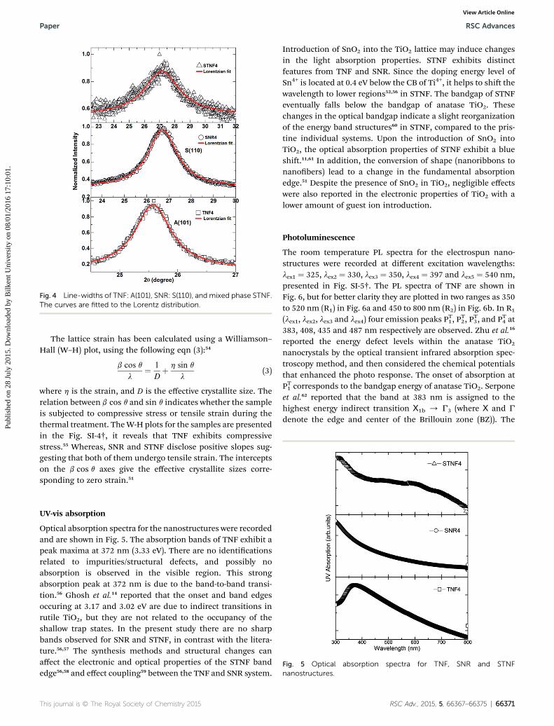
Fig. 4 Line-widths of TNF: A(101), SNR: S(110), and mixed phase STNF.The curves are fitted to the Lorentz distribution.
Paper RSC Advances
Publ
ishe
d on
28
July
201
5. D
ownl
oade
d by
Bilk
ent U
nive
rsity
on
08/0
1/20
16 1
7:10
:01.
View Article Online
The lattice strain has been calculated using a Williamson–Hall (W–H) plot, using the following eqn (3):54
b cos q
l¼ 1
Dþ h sin q
l(3)
where h is the strain, and D is the effective crystallite size. Therelation between b cos q and sin q indicates whether the sampleis subjected to compressive stress or tensile strain during thethermal treatment. TheW-H plots for the samples are presentedin the Fig. SI-4†, it reveals that TNF exhibits compressivestress.55 Whereas, SNR and STNF disclose positive slopes sug-gesting that both of them undergo tensile strain. The interceptson the b cos q axes give the effective crystallite sizes corre-sponding to zero strain.51
Fig. 5 Optical absorption spectra for TNF, SNR and STNFnanostructures.
UV-vis absorption
Optical absorption spectra for the nanostructures were recordedand are shown in Fig. 5. The absorption bands of TNF exhibit apeak maxima at 372 nm (3.33 eV). There are no identicationsrelated to impurities/structural defects, and possibly noabsorption is observed in the visible region. This strongabsorption peak at 372 nm is due to the band-to-band transi-tion.56 Ghosh et al.14 reported that the onset and band edgesoccuring at 3.17 and 3.02 eV are due to indirect transitions inrutile TiO2, but they are not related to the occupancy of theshallow trap states. In the present study there are no sharpbands observed for SNR and STNF, in contrast with the litera-ture.56,57 The synthesis methods and structural changes canaffect the electronic and optical properties of the STNF bandedge56,58 and effect coupling59 between the TNF and SNR system.
This journal is © The Royal Society of Chemistry 2015
Introduction of SnO2 into the TiO2 lattice may induce changesin the light absorption properties. STNF exhibits distinctfeatures from TNF and SNR. Since the doping energy level ofSn4+ is located at 0.4 eV below the CB of Ti4+, it helps to shi thewavelength to lower regions52,56 in STNF. The bandgap of STNFeventually falls below the bandgap of anatase TiO2. Thesechanges in the optical bandgap indicate a slight reorganizationof the energy band structures60 in STNF, compared to the pris-tine individual systems. Upon the introduction of SnO2 intoTiO2, the optical absorption properties of STNF exhibit a blueshi.11,61 In addition, the conversion of shape (nanoribbons tonanobers) lead to a change in the fundamental absorptionedge.51 Despite the presence of SnO2 in TiO2, negligible effectswere also reported in the electronic properties of TiO2 with alower amount of guest ion introduction.
Photoluminescence
The room temperature PL spectra for the electrospun nano-structures were recorded at different excitation wavelengths:lex1 ¼ 325, lex2 ¼ 330, lex3 ¼ 350, lex4 ¼ 397 and lex5 ¼ 540 nm,presented in Fig. SI-5†. The PL spectra of TNF are shown inFig. 6, but for better clarity they are plotted in two ranges as 350to 520 nm (R1) in Fig. 6a and 450 to 800 nm (R2) in Fig. 6b. In R1
(lex1, lex2, lex3 and lex4) four emission peaks PT1, PT2, P
T3, and PT4 at
383, 408, 435 and 487 nm respectively are observed. Zhu et al.16
reported the energy defect levels within the anatase TiO2
nanocrystals by the optical transient infrared absorption spec-troscopy method, and then considered the chemical potentialsthat enhanced the photo response. The onset of absorption atPT1 corresponds to the bandgap energy of anatase TiO2. Serponeet al.62 reported that the band at 383 nm is assigned to thehighest energy indirect transition Χ1b / G3 (where Χ and G
denote the edge and center of the Brillouin zone (BZ)). The
RSC Adv., 2015, 5, 66367–66375 | 66371
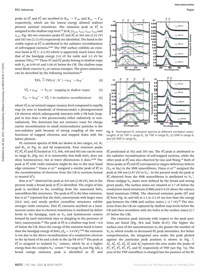
Fig. 6 Normalized PL emission spectra at different excitation wave-lengths of (a) TNF in range R1, (b) TNF in range R2, (c) SNR in range R1
and (d) SNR in range R2.
RSC Advances Paper
Publ
ishe
d on
28
July
201
5. D
ownl
oade
d by
Bilk
ent U
nive
rsity
on
08/0
1/20
16 1
7:10
:01.
View Article Online
peaks at PT2 and PT3 are ascribed to Χ2b / G1b, and Χ1a / G1b
respectively, which are the lowest energy allowed indirectphonon assisted transitions. The emission peak at PT4 isassigned to the shallow trap level.62 In R2 (lex1, lex2, lex3, lex4 andlex5, Fig. 6b) two emission peaks PT5 and PT6 at 562 nm (2.21 eV)and 585 nm (2.12 eV) respectively are identied. The band in thevisible region at PT5 is attributed to the radiative recombinationof self-trapped excitons.63,64 The TNF surface exhibits an emis-sion band at PT5 (�2.2 eV) which is apparently much lower thanthat of the bandgap energy (3.0 eV for rutile and 3.2 eV foranatase TiO2).16,62 These P
T5 and PT6 peaks belong to shallow traps
with VO at 0.99 eV and 1.08 eV below the CB. The shallow trapsmost likely concern VO at various energies. The green emissionscan be described by the following mechanism:62
TiO2 /hn
TiO2ðe�=hþÞ/eCB� þ hVB
þ (4)
V0O + eCB
� / VO (e� trapping in shallow traps) (5)
VO / hVB+ / V0
O + hn (radiative recombination) (6)
where V0O is an ionized oxygen vacancy level composed to rapidly
trap (in tens to hundreds of femtoseconds) a photogeneratedCB electron which subsequently interacts with a VB hole (trap-ped in less than a few picoseconds) either radiatively or non-radiatively. The dominant but not exclusive route for chargecarrier recombination in small semiconductor particles is thenon-radiative path because of strong coupling of the wavefunctions of trapped electrons and trapped holes with thelattice phonon.
PL emission spectra of SNR are shown in two ranges, viz. R1
and R2, in Fig. 6c and 6d respectively. Four emission peaksPS1, P
S2, P
S3 and PS4 located at 372, 406, 440 and 492 nm can be seen
in range R1 (Fig. 6c). It is noteworthy that bulk SnO2 does notshow luminescence, but at lower dimensions it does.65,66 Thepeak at PS1 with violet emission might be due to the near bandedge emission.31 Viana et al.13 assigned a similar peak of PS1 tothe recombination of electrons from the CB to excitons boundto neutral D0x.
Kim et al.67 observed the peak at 416 nm (2.98 eV), but in thepresent study a broad peak at PS2 is identied. The origin of thispeak is ascribed to Sni resulting from the nanosized SnO2
nanoribbon-like structures. The peak at PS3 is the blue emission.Kar et al.31 reported that the SnO2 nanocrystals with larger sizes(26.6 nm) and nearly perfect crystalline structures exhibitstronger violet emission. This PS3 emission ascribed as a lumi-nescent centre due to electron transitions is mediated by defectlevels in the bandgap, such as VO and luminescent centersformed by such interstitial sites or dangling in the presence ofSnO2 nanocrystals.45 The peak at PS4 is a shallow trap level �0.8eV below the CB. Since the energy of the emission band is lowerthan the bandgap energy of SnO2 (Eg ¼ 3.6 eV),13,68 the emissionis not due to the direct recombination of a conduction electronin the 4p band of Sn and a hole in the 2p VB of O.69 The peak atPS4 is assigned to isolated VO
+ centers, which lie at a higherenergy than the complex VO
+ center.13 In range R2 (see Fig. 6d), abroad orange emission peak is identied as PS5 and
66372 | RSC Adv., 2015, 5, 66367–66375
PS6 positioned at 562 and 585 nm. The PS5 peak is attributed tothe radiative recombination of self-trapped excitons, while theother peak at PS6 was also observed by Gao and Wang.70 Both ofthese peaks at PS5 and PS6 correspond to oxygen deciency defects(VO or Sni) in the SNR nanoribbons. Viana et al.13 assigned thepeak at 599 nm (2.07 eV) to VO
+. In the present study the peak atPS6 observed from the SNR nanoribbons is attributed to VO
+.These midgap VO states were dened by the broad and stronggreen peaks. The surface states are situated at 2.7 eV below theconduction bandminimum (CBM) and 0.9 eV above the valenceband maximum (VBM). The observed emission peaks (PS5 andPS6 from Fig. 6c and 6d) at 2.1 to 2.2 eV are less than the energygap between the CBM and surface states (�2.7 eV).68 The elec-trons from the CB are captured by shallow trap levels below theCB and then recombine with the holes at the surface states (2.7eV below the CB).
The emission peak intensity with respect to the peak posi-tions are listed (Fig. SI-6 and Table SI-2†). The higher thesurface area of the nanostructures is, the greater the number ofVO is, which results in decreased PL peak intensities. For bettercomprehension, the integrated area under the peak plottedagainst the particular peak position is shown in Fig. 7.AT1, A
T2, A
T3, A
T4, A
T5 and AT
6 represent the area under the peaks ofPT1, P
T2, P
T3, P
T4, P
T5, and PT6 respectively of TNF (see Fig. 7a). The
area of the TNF nanobers is changed but the position of the PL
This journal is © The Royal Society of Chemistry 2015
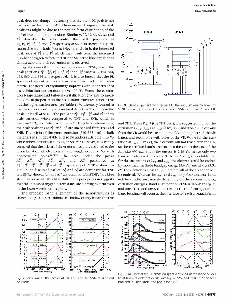
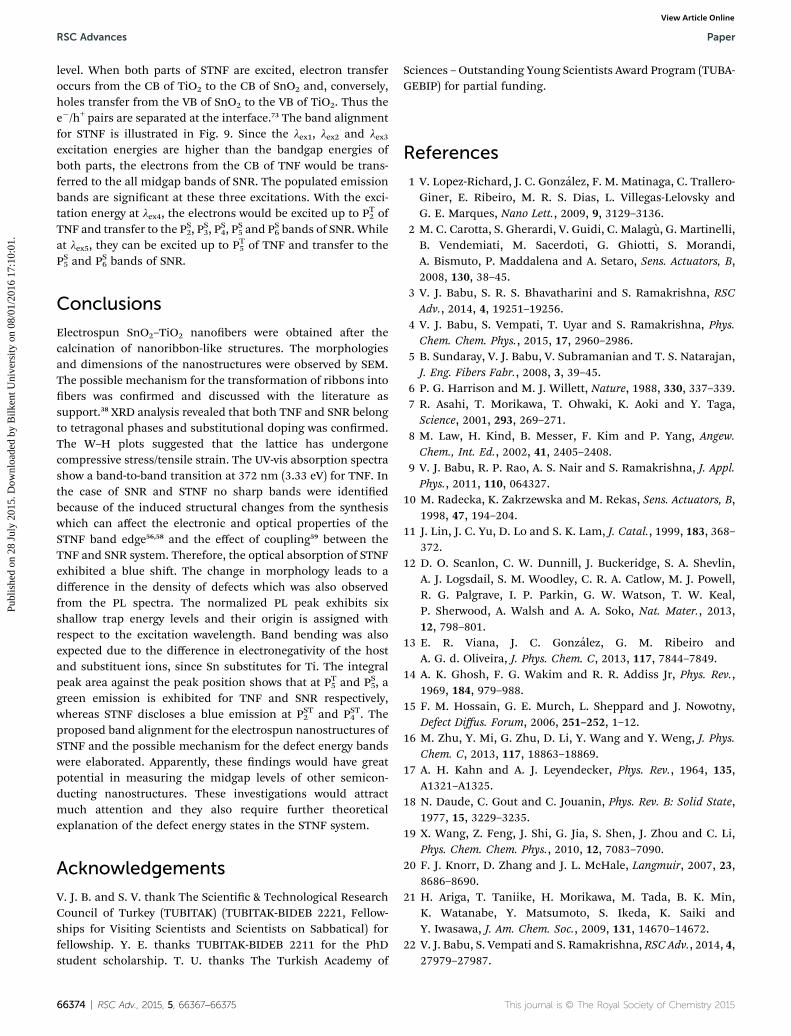
Fig. 9 Band alignment with respect to the vacuum energy level forSTNF, where [a] represents the bandgap of SNR as from ref. 13 and 68.
Paper RSC Advances
Publ
ishe
d on
28
July
201
5. D
ownl
oade
d by
Bilk
ent U
nive
rsity
on
08/0
1/20
16 1
7:10
:01.
View Article Online
peak does not change, indicating that the main PL peak is notthe intrinsic feature of TiO2. These minor changes in the peakpositions might be due to the non-uniform distribution of thedefect levels at nanodimensions. Similarly, AS
1, AS2, A
S3, A
S4, A
S5, and
AS6 describe the area under the peak positions at
PS1, PS2, P
S3, P
S4, P
S5 and PS6 respectively of SNR, as shown in Fig. 7b.
Noticeable from both gures (Fig. 7a and 7b) is the increasedpeak area at PT5 and PS5 which may result from the increasednumber of oxygen defects in TNF and SNR. The blue emission isalmost zero and only red emission is observed.
Fig. 8a shows the PL emission spectra of STNF, where thepeak positions PST1 , PST2 , PST3 , PST4 , PST5 and PST6 are at 373, 412, 433,488, 560 and 586 nm respectively. It is also known that the PLspectra of nanostructures are usually broad and oen asym-metric. The degree of crystallinity improves with the increase ofthe calcination temperature above 400 �C. Hence the calcina-tion temperature and tailored crystallization give rise to modi-ed optical properties in the SNTF nanostructures. Since STNFhas the higher surface area (see Table 1), VO are easily formed inthe nanobers resulting in structural defects at Ti centres in thebasic unit cell of STNF. The peaks at PST1 , PST2 , PST3 and PST4 showlittle variation when compared to TNF and SNR, which isbecause SnO2 is substituted into the TiO2 system. Interestingly,the peak positions at PST5 and PST6 are unchanged from TNF andSNR. The origin of the green emission (540–555 nm) in bulkmaterials is still debatable and some authors attribute it to VO
while others attributed it to Tii or Sni.14,32 However, it is widelyaccepted that the origin of the green emission is assigned to therecombination of electrons in the single occupied VO withphotoexcited holes.64,71,72 The area under the peaksAST1 , AST
2 , AST3 , AST
4 , AST5 , and AST6 positioned at
PST1 , PST2 , PST3 , PST4 , PST5 and PST6 respectively of STNF is shown inFig. 8b. As discussed earlier, AT
5 and AS5 are dominant for TNF
and SNR, whereas AST2 and AST
4 are dominant for STNF, i.e. a blueshi has occurred. This blue shi in the peak position suggeststhat the increased oxygen defect states are starting to form evenin the lower wavelength regions.
The proposed band alignment of the nanostructures isshown in Fig. 9. Fig. 9 exhibits six shallow energy bands for TNF
Fig. 7 Area under the peaks of (a) TNF and (b) SNR at differentpositions.
This journal is © The Royal Society of Chemistry 2015
and SNR. From Fig. 9 (the TNF part), it is suggested that for theexcitations lex1, lex2 and lex3 (3.82, 3.78 and 3.54 eV), electronsfrom the VB would be excited to the CB and populate all the sixbands and recombine with holes at the VB. While for the exci-tation at lex4 (3.12 eV), the electrons will not reach even the CB,so there are four bands seen near to the CB. In the case of thelex5 (2.3 eV) excitation, the energy is 2.29 eV, hence only twobands are observed. From Fig. 9 (the SNR part), it is notable thatfor the excitations at lex1 and lex2, the electron could be excitedby more than the SnO2 bandgap energy (3.6 eV) and at lex3 (3.54eV) the electron is close to Eg, therefore, all of the six bands willbe emitted. Whereas for lex4 and lex5, only four and one bandwill be emitted respectively depending on their correspondingexcitation energies. Band alignment of STNF is shown in Fig. 9,and once TiO2 and SnO2 contact each other to form a junction,band bending will occur at the interface to reach an equal Fermi
Fig. 8 (a) Normalized PL emission spectra of STNF in the range of 350to 800 nm at different excitations (lex ¼ 325, 330, 350, 397 and 540nm) and (b) area under the peaks for STNF.
RSC Adv., 2015, 5, 66367–66375 | 66373
RSC Advances Paper
Publ
ishe
d on
28
July
201
5. D
ownl
oade
d by
Bilk
ent U
nive
rsity
on
08/0
1/20
16 1
7:10
:01.
View Article Online
level. When both parts of STNF are excited, electron transferoccurs from the CB of TiO2 to the CB of SnO2 and, conversely,holes transfer from the VB of SnO2 to the VB of TiO2. Thus thee�/h+ pairs are separated at the interface.73 The band alignmentfor STNF is illustrated in Fig. 9. Since the lex1, lex2 and lex3
excitation energies are higher than the bandgap energies ofboth parts, the electrons from the CB of TNF would be trans-ferred to the all midgap bands of SNR. The populated emissionbands are signicant at these three excitations. With the exci-tation energy at lex4, the electrons would be excited up to PT2 ofTNF and transfer to the PS2, P
S3, P
S4, P
S5 and PS6 bands of SNR. While
at lex5, they can be excited up to PT5 of TNF and transfer to thePS5 and PS6 bands of SNR.
Conclusions
Electrospun SnO2–TiO2 nanobers were obtained aer thecalcination of nanoribbon-like structures. The morphologiesand dimensions of the nanostructures were observed by SEM.The possible mechanism for the transformation of ribbons intobers was conrmed and discussed with the literature assupport.38 XRD analysis revealed that both TNF and SNR belongto tetragonal phases and substitutional doping was conrmed.The W–H plots suggested that the lattice has undergonecompressive stress/tensile strain. The UV-vis absorption spectrashow a band-to-band transition at 372 nm (3.33 eV) for TNF. Inthe case of SNR and STNF no sharp bands were identiedbecause of the induced structural changes from the synthesiswhich can affect the electronic and optical properties of theSTNF band edge56,58 and the effect of coupling59 between theTNF and SNR system. Therefore, the optical absorption of STNFexhibited a blue shi. The change in morphology leads to adifference in the density of defects which was also observedfrom the PL spectra. The normalized PL peak exhibits sixshallow trap energy levels and their origin is assigned withrespect to the excitation wavelength. Band bending was alsoexpected due to the difference in electronegativity of the hostand substituent ions, since Sn substitutes for Ti. The integralpeak area against the peak position shows that at PT5 and PS5, agreen emission is exhibited for TNF and SNR respectively,whereas STNF discloses a blue emission at PST2 and PST4 . Theproposed band alignment for the electrospun nanostructures ofSTNF and the possible mechanism for the defect energy bandswere elaborated. Apparently, these ndings would have greatpotential in measuring the midgap levels of other semicon-ducting nanostructures. These investigations would attractmuch attention and they also require further theoreticalexplanation of the defect energy states in the STNF system.
Acknowledgements
V. J. B. and S. V. thank The Scientic & Technological ResearchCouncil of Turkey (TUBITAK) (TUBITAK-BIDEB 2221, Fellow-ships for Visiting Scientists and Scientists on Sabbatical) forfellowship. Y. E. thanks TUBITAK-BIDEB 2211 for the PhDstudent scholarship. T. U. thanks The Turkish Academy of
66374 | RSC Adv., 2015, 5, 66367–66375
Sciences –Outstanding Young Scientists Award Program (TUBA-GEBIP) for partial funding.
References
1 V. Lopez-Richard, J. C. Gonzalez, F. M. Matinaga, C. Trallero-Giner, E. Ribeiro, M. R. S. Dias, L. Villegas-Lelovsky andG. E. Marques, Nano Lett., 2009, 9, 3129–3136.
2 M. C. Carotta, S. Gherardi, V. Guidi, C. Malagu, G. Martinelli,B. Vendemiati, M. Sacerdoti, G. Ghiotti, S. Morandi,A. Bismuto, P. Maddalena and A. Setaro, Sens. Actuators, B,2008, 130, 38–45.
3 V. J. Babu, S. R. S. Bhavatharini and S. Ramakrishna, RSCAdv., 2014, 4, 19251–19256.
4 V. J. Babu, S. Vempati, T. Uyar and S. Ramakrishna, Phys.Chem. Chem. Phys., 2015, 17, 2960–2986.
5 B. Sundaray, V. J. Babu, V. Subramanian and T. S. Natarajan,J. Eng. Fibers Fabr., 2008, 3, 39–45.
6 P. G. Harrison and M. J. Willett, Nature, 1988, 330, 337–339.7 R. Asahi, T. Morikawa, T. Ohwaki, K. Aoki and Y. Taga,Science, 2001, 293, 269–271.
8 M. Law, H. Kind, B. Messer, F. Kim and P. Yang, Angew.Chem., Int. Ed., 2002, 41, 2405–2408.
9 V. J. Babu, R. P. Rao, A. S. Nair and S. Ramakrishna, J. Appl.Phys., 2011, 110, 064327.
10 M. Radecka, K. Zakrzewska and M. Rekas, Sens. Actuators, B,1998, 47, 194–204.
11 J. Lin, J. C. Yu, D. Lo and S. K. Lam, J. Catal., 1999, 183, 368–372.
12 D. O. Scanlon, C. W. Dunnill, J. Buckeridge, S. A. Shevlin,A. J. Logsdail, S. M. Woodley, C. R. A. Catlow, M. J. Powell,R. G. Palgrave, I. P. Parkin, G. W. Watson, T. W. Keal,P. Sherwood, A. Walsh and A. A. Soko, Nat. Mater., 2013,12, 798–801.
13 E. R. Viana, J. C. Gonzalez, G. M. Ribeiro andA. G. d. Oliveira, J. Phys. Chem. C, 2013, 117, 7844–7849.
14 A. K. Ghosh, F. G. Wakim and R. R. Addiss Jr, Phys. Rev.,1969, 184, 979–988.
15 F. M. Hossain, G. E. Murch, L. Sheppard and J. Nowotny,Defect Diffus. Forum, 2006, 251–252, 1–12.
16 M. Zhu, Y. Mi, G. Zhu, D. Li, Y. Wang and Y. Weng, J. Phys.Chem. C, 2013, 117, 18863–18869.
17 A. H. Kahn and A. J. Leyendecker, Phys. Rev., 1964, 135,A1321–A1325.
18 N. Daude, C. Gout and C. Jouanin, Phys. Rev. B: Solid State,1977, 15, 3229–3235.
19 X. Wang, Z. Feng, J. Shi, G. Jia, S. Shen, J. Zhou and C. Li,Phys. Chem. Chem. Phys., 2010, 12, 7083–7090.
20 F. J. Knorr, D. Zhang and J. L. McHale, Langmuir, 2007, 23,8686–8690.
21 H. Ariga, T. Taniike, H. Morikawa, M. Tada, B. K. Min,K. Watanabe, Y. Matsumoto, S. Ikeda, K. Saiki andY. Iwasawa, J. Am. Chem. Soc., 2009, 131, 14670–14672.
22 V. J. Babu, S. Vempati and S. Ramakrishna, RSC Adv., 2014, 4,27979–27987.
This journal is © The Royal Society of Chemistry 2015
Paper RSC Advances
Publ
ishe
d on
28
July
201
5. D
ownl
oade
d by
Bilk
ent U
nive
rsity
on
08/0
1/20
16 1
7:10
:01.
View Article Online
23 M. Norek, M. Michalska-Domanska, W. J. Stepniowski,I. Ayala, A. Bombalska and B. Budner, Appl. Surf. Sci., 2013,287, 143–149.
24 B. Liu, C. W. Cheng, R. Chen, Z. X. Shen, H. J. Fan andH. D. Sun, J. Phys. Chem. C, 2010, 114, 3407–3410.
25 J. Q. Hu, Y. Bando and D. Golberg, Chem. Phys. Lett., 2003,372, 758–762.
26 S. Luo, J. Fan, W. Liu, M. Zhang, Z. Song, C. Lin, X. Wu andP. K. Chu, Nanotechnology, 2006, 17, 1695–1699.
27 S.-S. Chang, S. O. Yoon and H. J. Park, Ceram. Int., 2005, 31,405–410.
28 F. Gu, S. F. Wang, C. F. Song, M. K. Lu, Y. X. Qi, G. J. Zhou,D. Xu and D. R. Yuan, Chem. Phys. Lett., 2003, 372, 451–454.
29 F. Gu, S. F. Wang, M. K. Lu, X. F. Cheng, S. W. Liu, G. J. Zhou,D. Xu and D. R. Yuan, J. Cryst. Growth, 2004, 262, 182–185.
30 Y.-C. Her, J.-Y. Wu, Y.-R. Lin and S.-Y. Tsai, Appl. Phys. Lett.,2006, 89, 043115.
31 A. Kar, S. Kundu and A. Patra, J. Phys. Chem. C, 2011, 115,118–124.
32 Ç. Kılıç and A. Zunger, Phys. Rev. Lett., 2002, 88, 095501.33 V. J. Babu, M. K. Kumar, A. S. Nair, T. L. Kheng,
S. I. Allakhverdiev and S. Ramakrishna, Int. J. HydrogenEnergy, 2012, 37, 8897–8904.
34 V. J. Babu, A. S. Nair, P. Zhu and S. Ramakrishna, Mater.Lett., 2011, 65, 3064–3068.
35 D. Li and Y. Xia, Adv. Mater., 2004, 16, 1151–1170.36 S. S. Lee, H. Bai, Z. Liu and D. D. Sun, Water Res., 2013, 47,
4059–4073.37 D. Li and Y. Xia, Nano Lett., 2003, 3, 555–560.38 M.-J. Paek, H.-W. Ha, T. W. Kim, S.-J. Moon, J.-O. Baeg,
J.-H. Choy and S.-J. Hwang, J. Phys. Chem. C, 2008, 112,15966–15972.
39 S. Zhang, L.-M. Peng, Q. Chen, G. H. Du, G. Dawson andW. Z. Zhou, Phys. Rev. Lett., 2003, 91, 256103.
40 R. Ma, Y. Bando and T. Sasaki, J. Phys. Chem. B, 2004, 108,2115–2119.
41 D. V. Bavykin, V. N. Parmon, A. A. Lapkin and F. C. Walsh, J.Mater. Chem., 2004, 14, 3370–3377.
42 U. Balachandran and N. G. Eror, J. Solid State Chem., 1982,42, 276–282.
43 S. Bakardjieva, V. Stengl, L. Szatmary, J. Subrt, J. Lukac,N. Murafa, D. Niznansky, K. Cizek, J. Jirkovsky andN. Petrova, J. Mater. Chem., 2006, 16, 1709–1716.
44 L. Abello, B. Bochu, A. Gaskov, S. Koudryavtseva,G. Lucazeau and M. Roumyantseva, J. Solid State Chem.,1998, 135, 78–85.
45 L. C. Nehru, V. Swaminathan and C. Sanjeeviraja, Am. J.Mater. Sci., 2012, 2, 6–10.
46 K. N. Yu, Y. Xiong, Y. Liu and C. Xiong, Phys. Rev. B: Condens.Matter Mater. Phys., 1997, 55, 2666–2671.
47 B. D. Cullity, Elements of X-ray diffraction, Addison-Wesleypublishing company, Inc., 1956, p. 42.
This journal is © The Royal Society of Chemistry 2015
48 B. D. Cullity, Elements of X-ray diffraction, Addison-Wesleypublishing company, Inc., 1956, p. 262.
49 L. Z. Liu, T. H. Li, X. L. Wu, J. C. Shen and P. K. Chu, J. RamanSpectrosc., 2012, 43, 1423–1426.
50 A. K. Tripathi, M. K. Singh, M. C. Mathpal, S. K. Mishra andA. Agarwal, J. Alloys Compd., 2013, 549, 114–120.
51 A. Maurya, P. Chauhan, S. K. Mishra and R. K. Srivastava, J.Alloys Compd., 2011, 509, 8433–8440.
52 Y. Cao, W. Yang, W. Zhang, G. Liu and P. Yue, New J. Chem.,2004, 28, 218–222.
53 T. Hirata, K. Ishioka, M. Kitajima and H. Doi, Phys. Rev. B:Condens. Matter Mater. Phys., 1996, 53, 8442–8448.
54 G. K. Williamson andW. H. Hall, Acta Metall., 1953, 1, 22–31.55 R. R. Prabhu and M. A. Khadar, Bull. Mater. Sci., 2008, 31,
511–515.56 E. Wang, T. He, L. Zhao, Y. Chen and Y. Cao, J. Mater. Chem.,
2011, 21, 144–150.57 A. K. Sinha, P. K. Manna, M. Pradhan, C. Mondal,
S. M. Yusuf and T. Pal, RSC Adv., 2014, 4, 208–211.58 X. Xu, G. Yang, J. Liang, S. Ding, C. Tang, H. Yang, W. Yan,
G. Yang and D. Yu, J. Mater. Chem. A, 2014, 2, 116–122.59 P. Du, L. Song, J. Xiong, N. Li, Z. Xi, L. Wang, D. Jin, S. Guo
and Y. Yuan, Electrochim. Acta, 2012, 78, 392–397.60 J. Zhang, W. Peng, Z. Chen, H. Chen and L. Han, J. Mater.
Chem. A, 2013, 1, 8453–8463.61 S. K. Zheng, T. M. Wang, W. C. Hao and R. Shen, Vacuum,
2002, 65, 155–159.62 N. Serpone, D. Lawless and R. Khairutdinov, J. Phys. Chem.,
1995, 99, 16646–16654.63 P. J. Young, C. Sun-Woo, A. Kandasami and K. S. Sub, J.
Nanosci. Nanotechnol., 2010, 10, 3604–3608.64 H. Tang, H. Berger, P. E. Schmid and F. Levy, Solid State
Commun., 1993, 87, 847–850.65 X. Wu, B. Zou, J. Xu, B. Yut, G. Tang, G. Zhangf andW. Chen,
Nanostruct. Mater., 1997, 8, 179–189.66 J. Hu, Y. Bando, Q. Liu and D. Golberg, Adv. Funct. Mater.,
2003, 13, 493–496.67 T. W. Kim, D. U. Lee and Y. S. Yoon, J. Appl. Phys., 2000, 88,
3759.68 X. T. Zhou, F. Heigl, M. W. Murphy, T. K. Sham, T. Regier,
I. Coulthard and R. I. R. Blyth, Appl. Phys. Lett., 2006, 89,213109.
69 M. H. Harunsani, F. E. Oropeza, R. G. Palgrave andR. G. Egdell, Chem. Mater., 2010, 22, 1551–1558.
70 T. Gao and T. Wang, Mater. Res. Bull., 2008, 43, 836–842.71 J. H. He, T. H. Wu, C. L. Hsin, K. M. Li, L. J. Chen,
Y. L. Chueh, L. J. Chou and Z. L. Wang, Small, 2006, 2,116–120.
72 X. Xiang, X. T. Zu, S. Zhu, L. M. Wang, V. Shutthanandan,P. Nachimuthu and Y. Zhang, J. Phys. D: Appl. Phys., 2008,41, 225102.
73 H. Shi, M. Zhou, D. Song, X. Pan, J. Fu, J. Zhou, S. Ma andT. Wang, Ceram. Int., 2014, 40, 10383–10393.
RSC Adv., 2015, 5, 66367–66375 | 66375