Embed Size (px)
Citation preview

© 2015 TechSearch International, Inc. www.techsearchinc.com
Expanding the Role of Fan-‐in and FO-‐WLP: Technology and Infrastructure Developments
E. Jan Vardaman, President and Founder, TechSearch InternaGonal
© 2015 TechSearch International, Inc. www.techsearchinc.com
Mobile Products ConGnue to Get Thinner
Source: ASE.
© 2015 TechSearch International, Inc. www.techsearchinc.com
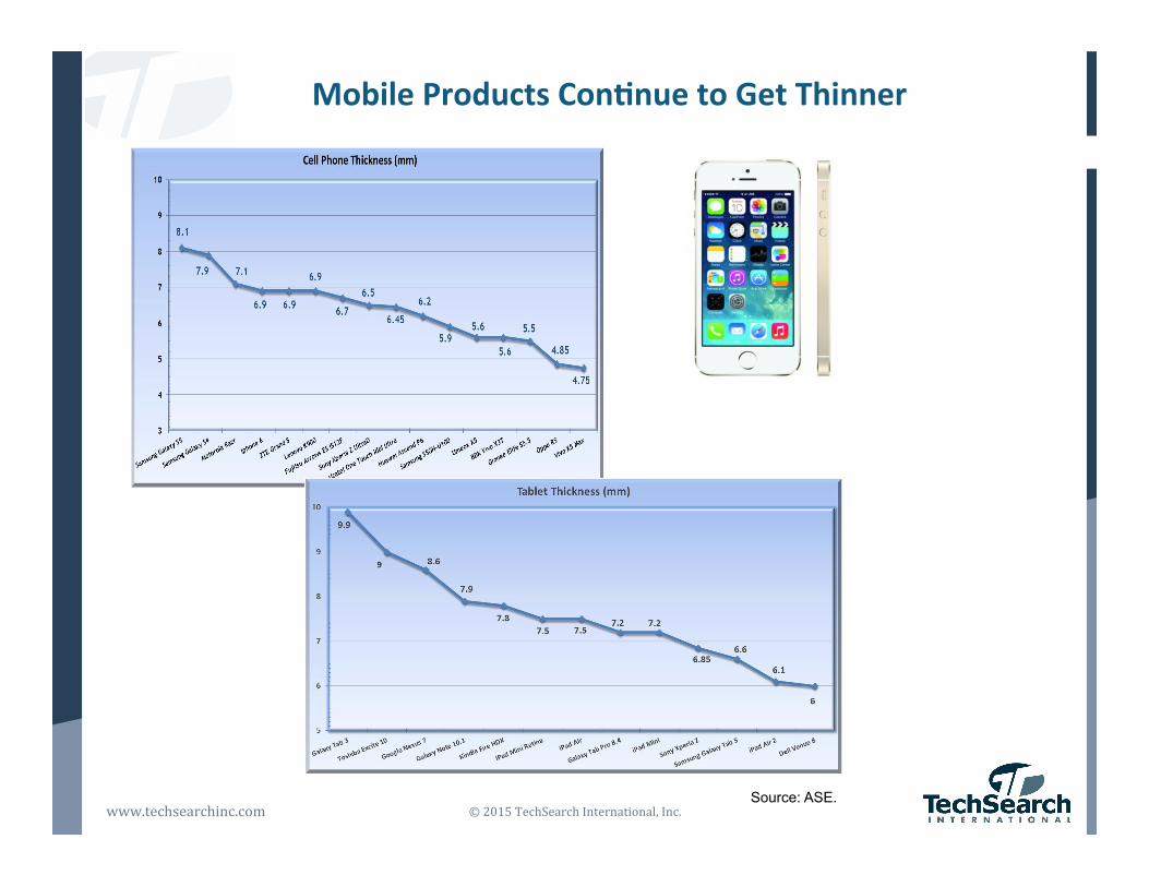
iPhone Trends: Increasing Number of WLPs
Source: ASE and TechSearch International, Inc., adapted from TPSS.
iPhone 3GS 2009 4 WLPs
iPhone 1 2007 2 WLPs
iPhone 4S 2011 7 WLPs
iPhone 5 2013 11+ WLPs
iPhone 5S 2013 22 WLPs
iPhone 6 2014 26+ WLPs
iPhone 6 Plus 2014 26+ WLPs
6
7
8
9
10
11
12
13
0
5
10
15
20
25
30
1 /2007 3GS /2009 4S /2011 5 /2012 5S /2013 6 /2014 6+ /2014
Thickness (mm)
WLCSPs
iPhone Model/year
iPhone Evolution
WLPs Thickness
Shown to scale

© 2015 TechSearch International, Inc. www.techsearchinc.com
Drivers for WLP
• Major applicaGons for WLP…… – Smartphones (highest volume applicaGon) – Digital cameras and camcorders – Laptops and tablets – Medical – AutomoGve – Wearable electronics such as watch
• WLP meets system packaging needs – Small form factor – Need for low profile packages – Lower cost (less material)
• Form Factor is Key – Low profile – Limited space on PCB

© 2015 TechSearch International, Inc. www.techsearchinc.com
ConvenGonal WLP ApplicaGons
• ConvenGonal WLPs for many device types (analog, digital, sensor, discrete) – Power management IC (PMIC) – Audio CODEC – RF – IPD, ESD protecGon, filter – LED driver – Electronic compass – Controller – MOSFET – CMOS image sensors – Ambient light sensors – EEPROM
• ConvenGonal WLPs trends – Highest I/O count 309 (Fujitsu power management IC) – Largest body size Qualcomm PMIC 6.5 mm x 6.5 mmx
0.71 mm, 0.4mm pitch – Increasing number of 0.4mm pitch parts, some 0.35mm
pitch – Fine pitch parts need high-‐density PCB to route signals
Source: ASE.

© 2015 TechSearch International, Inc. www.techsearchinc.com
Fan-‐In WLP Market ProjecGons
• ConvenGonal fan-‐in WLP demand • Growth driven by greater adopGon in smartphones, tablets, and wearable electronics
• CAGR of almost 9% from 2014 to 2019
0
10,000
20,000
30,000
40,000
50,000
2013 2014 2015 2016 2017 2018 2019
Millions'of'U
nits
Source:33TechSearch3International, Inc.

© 2015 TechSearch International, Inc. www.techsearchinc.com
Drivers for FO-‐WLP
• Smaller form factor, lower profile package: similar to convenGonal WLP in profile (can be ≤0.4 mm)
• Thinner than flip chip package (no substrate) – Can enable a low-‐profile PoP solu3on as large as
15mm x 15mm body • Support increased I/O density • Allows use of WLP with advanced semiconductor technology nodes with die shrinks – With increased I/O and smaller die can’t “fan-‐in”
using conven3onal WLP • Split die package or mulG-‐die package/SiP
– Mul3ple die in package possible – Die fabricated from different technology nodes can be assembled in a single package
– Can integrate passives • Excellent electrical and thermal performance • Excellent high temperature warpage performance • Improved board-‐level reliability • Fine L/S (10/10µm), roadmaps for (≤5/5µm)
Source: STATS ChipPAC.
Intel Wireless Division LTE analog baseband 5.32 x 5.04 x 0.7mm eWLB 127 balls, 0.4mm pitch
Source: TPSS.

© 2015 TechSearch International, Inc. www.techsearchinc.com
NANIUM’s eWLB Technology Roadmap
12 x 12
10/10
300 dia
120
75
Single Die
Multi-Die SbSw/ Passives
PoP Stacked-Die
50 30
80 50
300plus dia 450 dia rectangular
8/8 5/5 2/2
25 x 25 (SiP) 30 x 30 (SiP)
2x2 Double Side2x1 Double Side1x3 Single Side1x2 Single Side 1x4 Single Side
2014 2015 2016 2017
Package Size (mm )2
Line / Space (µm/µm)
Panel Size (mm)
Die-to-Die (µm)
Die-to-Pkg (µm)
Package Construction
Metallization Layers
(RDL & UBM)
Source: Nanium

© 2015 TechSearch International, Inc. www.techsearchinc.com
• 2 Layer-‐RDL InterconnecGon • 2 AcGve Die + 10 Passives 0201 SMD
After Molding
After Pick & Place
After Thin Film Processing, Solder Ball Attach and Singulation
MulG-‐Die/SiP FO-‐WLP SoluGon
Source: NANIUM

© 2015 TechSearch International, Inc. www.techsearchinc.com
FO-‐WLP for AutomoGve ApplicaGon Drivers
• Growth of acGve safety systems for automoGve applicaGons
• FO-‐WLP being adopted for mmWave applicaGons – Parking slot measurement (SRR) – Blind spot detec3on (SRR) – Adap3ve cruise control (LRR 77GHz)
– Emergency breaking – Lane correc3on
• Volumetric shrink of current and future systems (40 to 90%)
• Increased funcGonality with heterogeneous integraGon
• Improved in system performance – Low parasi3cs – Low inductance
• Improved board level reliability
Continental announced it is integrating Freescale’s 77GHz radar technology into its next generation short- and mid-range automotive radar modules
NXP radar module in FO-WLP
Source: NXP.
Source: Freescale.

© 2015 TechSearch International, Inc. www.techsearchinc.com
ApplicaGon Processor Packaging Trends
• Thinner package and smaller footprint – Today 1.0mm height requirement – Future ≤0.8 mm
• 3D IC with TSV provides the ulGmate in package height reducGon, but conGnues to be pushed out
• Silicon interposers too expensive for many mobile products
• PoP in high-‐end smartphones – Op3on 1: Con3nue with FC on thin
substrate – Op3on 2: Embedded AP in boaom
laminate substrate (MCeP) – Op3on 3: Fan-‐out WLP with
applica3on processor as boaom package
– Op3on 4: Some new format (SWIFT, NTI, etc.)
• FO-‐WLP AP in bokom PoP – Low profile – High rou3ng density – Handle high power – System integra3on with compe33ve
cost
Today’s PoP (1.0mm)
FO-WLP as Bottom PoP (<0.8mm)
© 2015 TechSearch International, Inc. www.techsearchinc.com
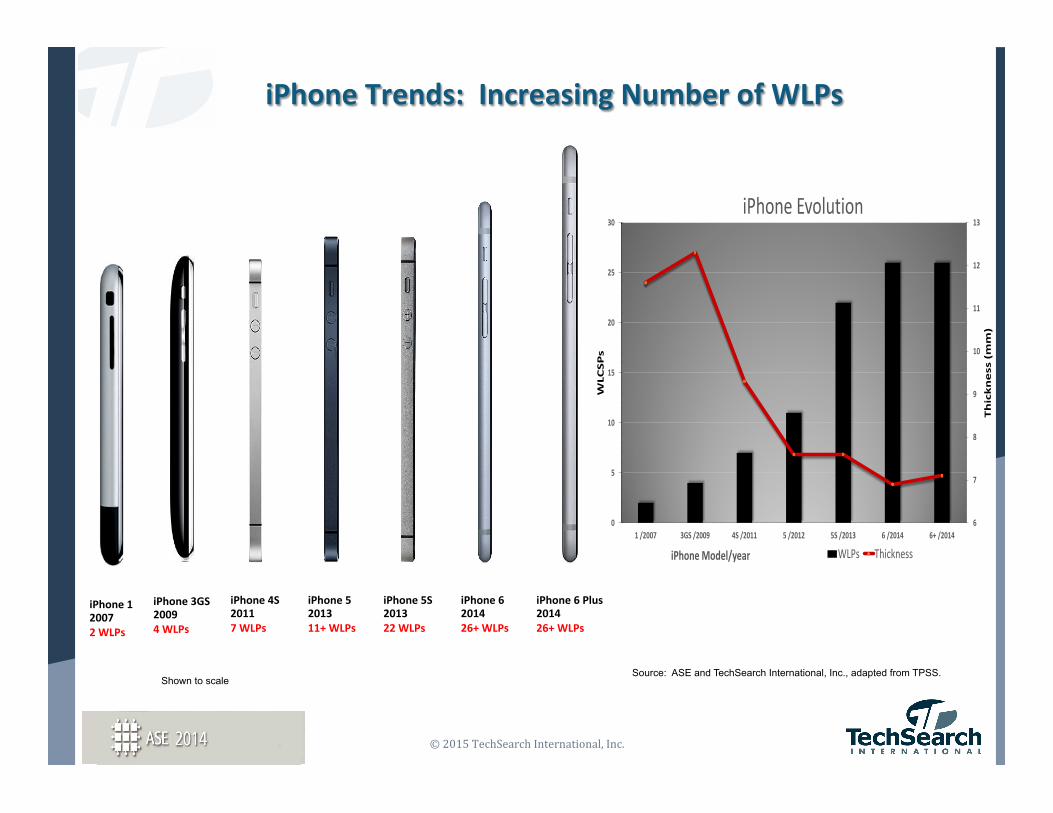
FO-‐WLP ProjecGons
• Early products included baseband processor (Infineon Wireless Division) • Device types include RF such as Bluetooth, NFC, GPS, PMIC, automoGve radar, future
applicaGon processors
0"
300"
600"
900"
1,200"
1,500"
1,800"
2,100"
2014" 2015" 2016" 2017" 2018" 2019"
Millions'of'U
nits'
Source:""TechSearch"Interna:onal,"Inc."

© 2015 TechSearch International, Inc. www.techsearchinc.com
FO-‐WLP Merchant Suppliers Status
• Amkor Technology redeploying FO-‐WLP with new 300mm line (eWLB) in K4 plant
• ADL Engineering 200mm pilot line in Taiwan • ASE license for Infineon’s eWLB with 300mm in Taiwan, also offers “chip last” panel version
• Deca Technologies (300mm “panel” format) • FCI/Fujikura (embedded WLP in flex circuit) • NANIUM (300mm wafer) license for Infineon’s eWLB • NEPES (300mm line in Korea) based on Freescale’s RCP process • PTI (R&D on panel) • SPIL (300mm wafer) • STATS ChipPAC (300mm wafer) will be purchased by JCET, license for Infineon’s eWLB
• TSMC (300mm wafer InFO WLP) • New suppliers TBD
© 2015 TechSearch International, Inc. www.techsearchinc.com
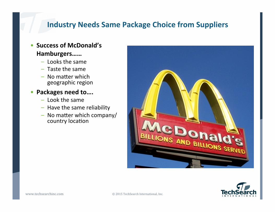
Industry Needs Same Package Choice from Suppliers
• Success of McDonald’s Hamburgers…… – Looks the same – Taste the same – No maaer which geographic region
• Packages need to…. – Look the same – Have the same reliability – No maaer which company/country loca3on

© 2015 TechSearch International, Inc. www.techsearchinc.com
ExcepGons to the McDonald’s Hamburger Rule
• When a foundry…. – Provides its foundry customer a packaging solu3on
– Enables faster 3me to market with silicon and package delivery
– Provides a warranty accepted by end customer
• When a company is verGcally integrated…. – From silicon design and fabrica3on to IC package and assembly to end product
• If same funcGon is accepted – Different process – Alterna3ve accepted with same func3on, performance, and reliability
© 2015 TechSearch International, Inc. www.techsearchinc.com
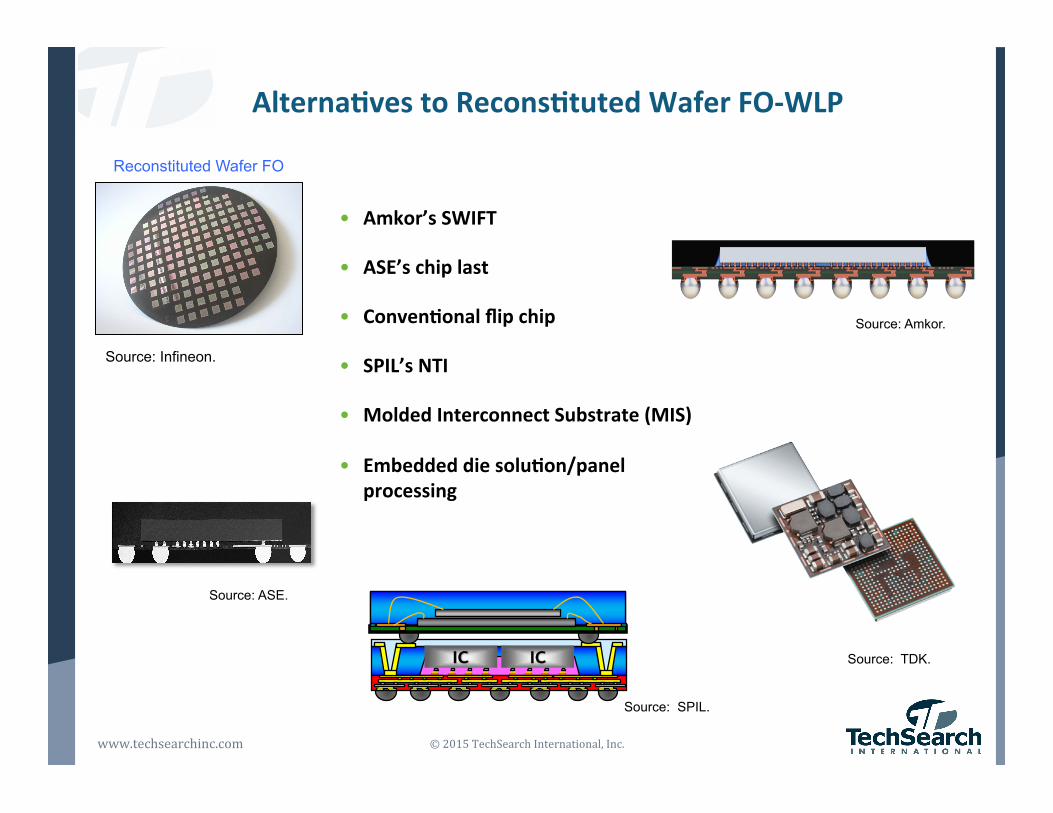
AlternaGves to ReconsGtuted Wafer FO-‐WLP
• Amkor’s SWIFT
• ASE’s chip last
• ConvenGonal flip chip
• SPIL’s NTI
• Molded Interconnect Substrate (MIS)
• Embedded die soluGon/panel processing
Source: Amkor.
Source: Infineon.
Source: ASE.
Source: TDK. IC IC
Source: SPIL.
Reconstituted Wafer FO
© 2015 TechSearch International, Inc. www.techsearchinc.com
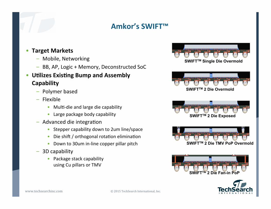
Amkor’s SWIFT™
• Target Markets – Mobile, Networking – BB, AP, Logic + Memory, Deconstructed SoC
• UGlizes ExisGng Bump and Assembly Capability – Polymer based – Flexible
• Mul3-‐die and large die capability • Large package body capability
– Advanced die integra3on • Stepper capability down to 2um line/space • Die shig / orthogonal rota3on elimina3on • Down to 30um in-‐line copper pillar pitch
– 3D capability • Package stack capability
using Cu pillars or TMV
SWIFTTM Single Die Overmold
SWIFTTM 2 Die Overmold
SWIFTTM 2 Die Exposed
SWIFTTM 2 Die TMV PoP Overmold
SWIFTTM 2 Die Fan-in PoP

© 2015 TechSearch International, Inc. www.techsearchinc.com
ASE’s Chip’s Last Package
• Uses low-‐cost coreless substrate – Fine pitch capable (15 L/S today, 12µm L/S
development) – Manufactured in double panel format – Assembled in strip format – Mul3-‐die and passives possible – Can be boaom PoP
• Thin package (<375 µm) • High current and thermal handling capabiliGes
– Due to thicker Cu (15-‐20 µm) • Uses exisGng FC infrastructure
– Flip chip with Cu pillar mounted on coreless substrate
– Mass reflow and molded underfill
Source: ASE.

© 2015 TechSearch International, Inc.
Panel Size: 510x410 mm (209, 100mm2) X 2 Strip Size: 240x76.2 mm (X2L) Strip Array: 34x13 => 442 ea
Wafer size : 300mm(70,686mm2)
Fan Out Chip Last Panel vs Wafer UGlizaGon
6:1 Area
Source: ASE.

© 2015 TechSearch International, Inc. www.techsearchinc.com
Molded Interconnect Substrate
• MIS-‐BGA offered by JCET (owns APS) and SPIL • Versions offered by other OSATs
Wire%bond%Terminal
External%Terminal
Top%View
Bo5om%View
Carrier
Outer)Lead)with)NiPdAu)or)OSP
Outer)Lead)with)NiPdAu)or)OSP
Inner)Lead)for)WB)or)FC
Source: JCET.
© 2015 TechSearch International, Inc. www.techsearchinc.com
Is Panel Processing a Viable AlternaGve?
• What size panel is feasible? • Assembly of die on panel
– Die placement accuracy may be more difficult to control with large panels – Large area bonders may be required – Throughput (3me required to pick and place die in panel) – How is placement accuracy impacted by tape and mold compound? – What level of inspec3on is required to verify accuracy? What speed?
• Dielectric dispense methods? – How to control run-‐out at edge? – Need inspec3on for even coa3ng?
• Molding materials and process? • Panel warpage
– Warpage increases with panel size – Impact of materials (mold compound and filler) – What type of inspec3on is requires and how will it work with warped panels
• Via formaGon method (minimum via diameter) – Via alignment
• Metal plaGng – Metal to dielectric interface (what inspecGon requirements?) – How to spuker seed layer?
• Interconnect reliability? InspecGon for broken metal traces etc. • SingulaGon method? • Solder ball placement and inspecGon method?

© 2015 TechSearch International, Inc. www.techsearchinc.com
AddiGonal ConsideraGons for Panel Processing
• Warpage (impacts assembly/manufacturability) – Heterogeneous materials and non-‐
symmetric structures can cause bowing
– Polymer materials with adapted CTE and modulus, plus low shrink
• Accuracy/resoluGon (miniaturizaGon) – Improved op3cal recogni3on
systems for placement equipment – Imaging with high depth of focus
and high resolu3on • Yield (impacts cost)
– Suited materials and components – Op3mized processes – Produc3on experience
Source: Fraunhofer IZM.

© 2015 TechSearch International, Inc. www.techsearchinc.com
Conclusions
• Mobile products require low profile packages – Fan-‐in WLP – FO-‐WLP
• Demand for lower cost soluGons drives adopGon of new package designs and formats – Round panels? – New chip last packages? – MIS on modified leadframe? – Large area processing?
• Many package choices – Few standard op3ons except conven3onal WLP – Growing number of companies selec3ng FO-‐WLP with recons3tuted wafer
– Alterna3ves will con3nue to be developed

© 2015 TechSearch International, Inc. www.techsearchinc.com
Thank you!
TechSearch Interna3onal, Inc. 4801 Spicewood Springs Road, Suite 150
Aus3n, Texas 78759 USA +1.512.372.8887