Embed Size (px)
DESCRIPTION
lab purpose
Citation preview

EXPERIMENT NO: –1 AIM : Study of V-I Characteristics of a Diode. APPARATUS REQUIRED : Diode Characteristics Kit , Power Supply, Ammeter (0-20mA), Voltmeter (0-20V), Connecting Leads. BRIEF THEORY : A P-N junction is known as Semiconductor diode or Crystal diode. It is the combination of P-type & N-type Semiconductor. Which offers Nearly zero resistance to current on forward biasing & nearly infinite Resistance to the flow of current when in reverse biased. Forward biasing : When P-type semiconductor is connected to the +ve terminal and N-type to –ve terminal of voltage source. Nearly zero resistance is offered to the flow of current. Reverse biasing : When P-type semiconductor is connected to the –ve terminal and N-type to +ve Terminal. Nearly zero current flow in this condition. CIRCUIT DIGRAM : (1) When diode is forward biased (2) When diode is reverse biased
V
BT2
12
mAmA
V D10
R2A1 16
R2A1 16
BT2
12
D10
PROCEDURE :
(1) Connect the ckt. as shown in fig. (2) Switch on the power supply. (3) Vary the value of input dc supply in steps. (4) Note down the ammeter & voltmeter readings for each step. (5) Plot the graph of Voltage Vs Current.
(6) Connect the ckt. as shown in fig.

OBSERVATION TABLE :
When Diode Is Forward Biased
When Diode Is Reverse Biased
S.NO.
Current(mA) Voltage(V) Current [µA)
Voltage(V)
1. 2. 3.
GRAPH :
RESULT : The graph has been ploted between voltage and current. DISCUSSION: The diode donot conduct in RB state and conduct in FB state. PRECAUTIONS : (1)Always connect the voltmeter in parallel & ammeter in series as shown in fig.
(2)Connection should be proper & tight. (3)Switch ‘ON’ the supply after completing the ckt. (4)DC supply should be increased slowly in steps (5)Reading of voltmeter & Ammeter should be accurate.
QUIZ : Q.1 Define semiconductor diode ? A. A PN – junction is called semiconductor diode. Q.2 Define depilation layer ? A. The region having uncompensated acceptor and donor ions. Q.3 What do you mean by forward biased ? A. When +ve terminal of battery is connected to P side & -ve terminal to N side of diode. Q.4 What do you mean by reverse biased ?

A. When +ve terminal of battery is connected to N side & -ve terminal to P side of diode. Q.5 Define Knee voltage ?
A. The forward voltage at which current through the junction starts increasing rapidly. Q.6 Define breakdown voltage ? A. Reverse voltage at which PN junction breaks down with sudden rise in reverse current. Q.7 Define max. forward current ?
A. It is highest instantaneous forward current that a PN junction can conduct without damage to Junction.
Q.8 Define max. power rating ? A. Max. power that can be dissipated at junction without damage to it.

EXPERIMENT NO : 2 AIM : Study of Half – Wave Rectifier . APPARATUS REQUIRED : Power supply, rectifier kit., CRO, Connecting Leads. BRIEF THEORY : Rectification is a process of conversion of AC to DC . In half-wave rectifier, only one diode is used . During +ve half Cycle the diode is forward biased &, it conducts current through the load resistor R .During –ve half cycle diode is reverse biased Hence, no current flow through the circuit. Only +ve half cycle appears across the load, whereas, the –ve half Cycle is suppressed. CIRCUIT DIGRAM
:transformer
to CRO
T11 5
4 8
D1
DIODE230 V, 50 Hz AC suply
C
PROCEDURE :
(a) Connect the ckt. as shown in fig. (b) Supply the input AC signal to the circuit. (c) Output signal is obtained on CRO which shows the DC( pulsating output).
(d) Draw the wave form. WAVE FORM :
Input wave

Output wave
RESULT : Input and output waveform of half wave rectifier is as shown. Discussion: The output obtained is unidirectional, pulsating DC . but ripple factor is large. PRECAUTIONS :
(a) Connection should be proper & tight. (b) Switch ‘ON’ the supply after completing the ckt. (c) Note down the input & output wave accurately.
QUIZ : Q.1 Define Rectifier ? A. A circuit used to convert a.c. voltage into the pulsating d.c. voltage. Q.2 What is Half-Wave Rectifier ? A. Rectifier in which diode conduct only for half cycle of waveform. Q.3 Define PIV ? A. Max. voltage which a diode can withstand without breakdown in reverse bias conditon. Q.4 What type of output we get from H-W Rectifier ? A. In output we get unidirectional pulsating voltage. Q.5 Write its Disadvantage ? A. Rectification efficiecy is less & ripple factor is more. Q.6 Define efficiency . A. Ratio of d.c. power delivered to the load to the a.c. i/p power from sec. wdg. of transformer. Q.7 Define Ripple Factor ? A. It is a measure of purity of output of a rectifier. Q.8 What is the value of Rf for H-W Rectifier ? A. 1.21 Q. 9 What is Transformer utilization factor ? A. Ratio of d.c. power delivered to the load to the a.c. rating of transformer secondary. Q.10 What is the value of Irms for HW Rectifier ? A. Im/2.

EXPERIMENT NO : 3 AIM : Study of Full – Wave Rectifier . APPARATUS REQUIRED : Power Supply, Rectifier kit., CRO, Connecting Leads. BRIEF THEORY : In full-wave rectification, When A.C supplied at the input , both the half cycles current flows through the load in the same direction. The following two circuits are commonly employed.
Centre-tap full-wave Rectifier : In this rectifier, two diodes & a center-tap transformer is used . During +ve half cycle the diode D1 is forward biased & D2 is reverse biased .Output will be obtained across load resistor R .During –ve half cycle diode D1 is reverse biased &D2 is forward biased. Output will be obtained across load resistor R again & the direction of output is same i.e, DC output is obtained.
Bridge Rectifier : The ckt. contains four diodes connected to form a bridge. In this an ordinary Transformer is used. During +ve half cycle of secondary voltage, diodes D1 & D3 are forward biased & diodes D2& D4 are reverse biased & vice versa.
CIRCUIT DIGRAM
:
To CRO
C230 V, 50 Hz AC suply
transformer
T11 5
4 8D2
D1
PROCEDURE :
(d) Connect the ckt. as shown in fig. (e) Supply the input AC signal to the circuit. (f) Output signal is obtained on CRO which shows the DC( pulsating output). (g) Draw the wave form.

WAVE FORM :
Input wave
Output wave RESULT: The input and output waveforms of full wave rectifier has been drawn. Discussion : The output is unidirectional , pulsating dc . But ripple factor is less than half wave rectifier. PRECAUTIONS : (a)Connection should be proper & tight. (b)Switch ‘ON’ the supply after completing the ckt. (c)Note down the input & output wave accurately.
QUIZ : Q.1 Define Full wave rectifier ? A. In which diode conducts for both half cycles of waveform. Q.2 Different types of FW rectifier ? A. Center tapped & Bridge Rectifier. Q.3 Write PIV of Center tapped rectifier. A. 2Vm. Q.4 Define Form Factor ? A. It is ratio of r.m.s. value to average value. Q.5 Write ripple factor for FW rectifier ? A. 0.48 Q.6 What is the efficiency of FW rectifier ? A. 81.2% Q.7 Write advantages of bridge rectifier ? A. Diode’s PIV rating is Vm & it does not require Centre-tapped secondary winding. Q.8 Write disadvantage of bridge rectifier ? A. It requires 4 diodes so it can not be used for low voltage applications. Q.9 Write output frequency for FW rectifier ? A. 100 hz . Q.10 Write value for DC current ? A. 0.636 Im.

EXPERIMENT NO : 4
AIM: To Study the characteristics of transistor in Common Base configuration .
APPARATUS REQUIRED : Power supply, Transistor characteristics Kit, Connecting Leads, Voltmeter, Ammeter.
BRIEF THEORY : Transistor is a semiconductor device consist of two p-n junctions. It has three terminals, to handle I/P and O/P four terminals are needed . Therefore, one terminal is made common . A transistor can be connected in three Ways CB, CE, CC. Common base :
Base is made common. I/P is connected between base & emitter and O/P is taken between base & collector. Input charact. The curve plotted between emitter current I & the emitter-base voltage constant collector-base voltage V . Output charact. The curve plotted between collector current I & collector-base voltage V constant emitter current I. . CIRCUIT DIAGRAM :
PROCEDURE :
Input charact. (a) Make the connection as per circuit diagram . (b) Switch ‘ON’ the supply & set V = 0V (c) Vary V in step & note down the emitter current I at each step . (d) Set V = 1V & again repeat the same procedure . (e) Draw the graph.

Output charact. (a) Make the connection as per circuit diagram. (b) Set the value of I = 1mA (c) Vary V in step & note down the collector current I at each step. (d) Set I = 2mA & repeat the same procedure . (e) Draw the graph .
OBSERVATION TABLE :
Input charact.(Vcb=Cons.) Output charact. (Ie = Const.) S.No Ie(mA) Veb(Volts) Ic(mA) Vcb(Volts) 1. 2. 3.
GRAPH :
RESULT : The input and output characteristics of transformer in CB configuration has been plotted. DISCUSSION: With the help of output characteristics we can calculate ac & dc current gain in CB configuration. PRECAUTIONS :
(1) Always connect the voltmeter in parallel & ammeter in series as shown in fig. (2) Connection should be proper & tight. (3) Switch ‘ON’ the supply after completing the ckt. (4) DC supply should be increased slowly in steps (5) Reading of voltmeter & Ammeter should be accurate.

QUIZ: Q1: What do you mean by biasing of transistor? A. When dc voltages are applied across the different terminals of transistor, it is called biasing. Q2: What is d.c. current gain in common base configuration? A. It is ratio of collector current(Ic) to emitter current (Ie). Q3: What is typical value for d.c. current gain ? A. 0.99 Q4: What is a.c. current gain in CB confifuration? A. It is ratio of change in collector current to change in emitter current. Q5: What are input characteristics? A. These curves relate i/p current & i/p voltage for a given value of o/p voltage. Q6: What are output characteristics? A. Thes curves relate o/p voltage & o/p current for a given value of input current. Q7: Which configuration has highest voltage gain? A. Common Emitter. Q8: Which configuration is most widely used? A. Common Emitter. Q9: What is operating point? A. The zero signal values of Ic & Vce. Q10: Which reigon is heavily doped in Transistot? A. Emitter

EXPERIMENT NO :5 AIM : Study of characteristics of JFET in Common Source Configuration . APPARATUS REQUIRED : Power Supply, FET Characteristics Kit, Connecting Leads, Voltmeter, Ammeter. BRIEF THEORY : A FET is a three terminal semiconductor device in which current Conduction is by one type of carriers & is controlled by the effect of electric field. There are two types of FET namely JFET & MOSFET. Again, a JFET can either have N-channel or P-channel. A N-channel JFET has a N-type semiconductor bar, the two ends of which make the Drain & source terminal. On the two sides of this bar, P-N junction are made. These P region makes gate. Usually, these two gates are connected together to form a single gate .The gate is given a –ve bias w.r.t Source. Drain is given +ve potential w.r.t Source . CIRCUIT DIGRAM :
D
12
12
VGS
mA
S
2
3
1
VDS
G
PROCEDURE :
Drain characteristic (a) Connect the circuit as shown in fig. Keep V & V supplies at minimum.
(b) Switch ON power , Increase V gradually & note the max. current as I while the V =0V (c) Repeat the step for different values of V , & note corresponding I & V for increment. (d) Tabulate the results . Transfer characteristic
(a) Keep V fixed at 4V . (b) Increase V in small steps & note corresponding I for each step. (c) Repeat step 2 for different values of V . (d) Tabulate the results .

OBSERVATION TABLE :
Transfer charact.(Vds=Cons.) Drain charact. (Vgs= Const.) S.No Id(mA) Vgs(Volts) Id(mA) Vds(Volts) 1. 2. 3.
GRAPH :
RESULT : Transfer & Drain characteristics of JFET in common source configuration has been plotted. DISCUSSION: We obseve that characteristics has 4 regions: Ohmic region, curve AB, Pinch off region& Breakdown region. PRECAUTIONS :
(6) Always connect the voltmeter in parallel & ammeter in series as shown in fig. (7) Connection should be proper & tight. (8) Switch ‘ON’ the supply after completing the ckt. (9) DC supply should be increased slowly in steps (10) Reading of voltmeter & Ammeter should be accurate.
QUIZ : Q.1 Define FET ? A It is a 3 terminal device in which current conduction is by only one type of mazority carriers. Q.2 Define pinch off Voltage ? A. The value of Vds at which all the free charge carriers are removed from channel. Q.3 What is unipolar device ? A. In which conduction is by only one type of mazority carriers. Q.4 What is bipolar device ? A. In which conduction is by both types of carriers. Q.5 Write advantages of FET over conventional Transistor ? A. It provides extremely high input impedance as compared to BJT. Q.6 Define drain Characteristics ? A. The curve b/w drain current & Vds with Vgs as a parameter. Q.7 Define transfer Characteristics ? A. The curve b/w Id & Vgs keeping Vds constt.

Q.8 Write applications of a FET ? A. FETs are used in ICs, voltage – variable resistor in operational amplifier etc. Q.9 Input impedance of a FET is more than a BJT , Why ? A Because it always work in reverse biasing situation. Q.10 Define amplification factor ? A. Ratio of change in drain-source voltage to change in gate to source voltage at constt. Id.

EXPERIMENT NO 6
AIM:- To study the Common Emitter Configuration of BJT . APPARATUS REQUIRED : Transistor Characteristic kit , Multimeter, Connecting leads and Power Supply . THOREY :- In common Emitter configuration input is applied between base and emitter while the output is taken across emitter and collector. Thus the emitter forms the terminal common to doth input and output circuits. The load resistance is connected at collector.
CIRCUIT DIAGRAM :-
R
12
12
VCE
R
12V
mA1 16
mAIC1 16
VBE
IB
PROCEDURE :
(a) Connect the circuit as per the circuit diagram (b)
Input characteristics (c) Keep emitter - collector voltage constant. (d) Vary collector-base voltage in steps and note down base reading. (e) Readings are tabulated and graph is drawn
Output characteristics (a) Keep base current constant (b) Vary collector-emitter voltage in steps and note down emitter current (c) Readings are tabulared and graph is drawn
OBSERVATION TABLE :
Input charact.(Vce=Cons.) Output charact. (Ib = Const.) S.No Ib(mA) Vbe(Volts) Ic(mA) Vce(Volts) 1. 2. 3.

GRAPH:-
RESULT:-The input and output characteristic of transistor in common emitter configuration has been plotted. DISCUSSION : With the help of output characteristics we can calculate AC& DC current gain in common emitter configuration. PRECAUTIONS:
(a) Connections should be tight (b) Handle the equipments with care
QUIZ: Q.1 What is common collector configuration? A. In common collector configuration input is applied between base and collector while the output is taken across emitter and collector. Q. 2 . What is approximate value of input impedance of common collector configuration? A . Approximate value of input impedance of comm. collector configuration is 750 K Ω. Q. 3.What is approximate value of output impedance of common collector configuration? A Approximate value of output impedance of comm. collector configuration is 50 Ω. Q 4.What is approximate value of current gain of comm. collector configuration ?. A. Approximate value of current gain of comm. collector configuration is about 100. Q.5 What is approximate value of voltage gain of comm. collector configuration ?. A. Approximate value of voltage gain of comm. collector configuration is less than unity.
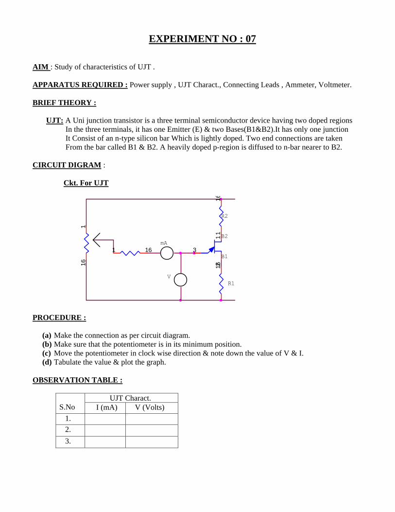
EXPERIMENT NO : 07 AIM : Study of characteristics of UJT . APPARATUS REQUIRED : Power supply , UJT Charact., Connecting Leads , Ammeter, Voltmeter. BRIEF THEORY : UJT: A Uni junction transistor is a three terminal semiconductor device having two doped regions In the three terminals, it has one Emitter (E) & two Bases(B1&B2).It has only one junction It Consist of an n-type silicon bar Which is lightly doped. Two end connections are taken From the bar called B1 & B2. A heavily doped p-region is diffused to n-bar nearer to B2. CIRCUIT DIGRAM : Ckt. For UJT
R2
116
mA
R1
B2
V
3
12
116
B1
16
1 16
PROCEDURE :
(a) Make the connection as per circuit diagram. (b) Make sure that the potentiometer is in its minimum position. (c) Move the potentiometer in clock wise direction & note down the value of V & I. (d) Tabulate the value & plot the graph.
OBSERVATION TABLE :
UJT Charact. S.No I (mA) V (Volts) 1. 2. 3.

GRAPH : UJT Charact.
RESULT: The characteristics of UJT has been plotted. PRECAUTION:
(1) Always connect the voltmeter in parallel & ammeter in series as shown in fig. (2)Connection should be proper & tight. (3)Switch ‘ON’ the supply after completing the ckt. (4)DC supply should be increased slowly in steps (5)Reading of voltmeter & Ammeter should be accurate.
QUIZ : Q.1 Define UJT ? A. It is a 2 layer, 3- terminal solid state device having only one junction. Q.2 Write application of UJT ? A. Relaxation oscillator. Q.3 Define inter base Resistance ? A. The total resistance of silicon bar from one end to other end. Q.4 Mention different region of UJT ? A. Cut – off region, negative resistance region, saturation region. Q.5 Define peak Point Emitter Current? A. Min. current that is reqd. to trigger the device. Q6. Define valley point Current ? A. It is the emitter current at valley point.

EXPERIMENT NO – 8 AIM : Study characteristics of Thyristor . APPRATUS REQUIRED : Power Supply , SCR Kit. , Voltmeter , Ammeter , Connecting Leads. BRIEF THEORY : Silicon control rectifier (SCR) is a four layer , three terminal semiconductor device, The end ‘P’ forms the anode & the end ‘N’ forms the cathode & the gate terminal ‘G’ is from the ‘P’ layer next to cathode. It is a unidirectional device. The device can exist upon either ON state or OFF state depending upon the applied voltage . When anode voltage is +ve w.r.t to cathode the SCR start Conducting. If some small gate voltage is applied, the SCR trigger at some low value of anode voltage, but it loses its all control on the SCR Current after triggering. Therefore, in order to turn the SCR to OFF position the anode voltage has to be reduced to zero. CIRCUIT DIGRAM :
K G
12
mA
12V
12
1 16mA
A
R1 16
V
R
PROCEDURE :
(a) Connect the circuit according to the fig. (b) First set I = 0mA , vary input voltage V gradually & measure the current I. (c) Tabulate the readings. (d) Repeat the procedure for different values of I . (e) Draw the graph between V & I .
OBSERVATION TABLE :
S.No
Vak(Volts)
Iak (mA)

GRAPH :
PRECAUTIONS : (1)Always connect the voltmeter in parallel & ammeter in series as shown in fig.
(2)Connection should be proper & tight. (3)Switch ‘ON’ the supply after completing the ckt. (4)DC supply should be increased slowly in steps (5)Reading of voltmeter & Ammeter should be accurate.
RESULT : The characteristics of thyristor has been plotted. Discussion: The SCR will not conduct until it is not triggered by gate voltage. QUIZ : Q.1 Define SCR?
A. It is a controlled rectifier constructed of a silicon material with third terminal for control purpose. Q.2 Define Forward Break over Voltage? A. It is voltage in forward conducting mode after which SCR starts conducting. Q.3 Define reverse Break down Voltage?
A. If reverse voltage is increased beyond certain value, SCR will break & this voltage is called reverse breakdown voltage.
Q.4 Why it is called controlled rectifier? A. Because its operation as rectifier can be controlled by using gate terminal. Q.5 Define peak forward Voltage? A. It is limiting positive anode voltage above which SCR get damaged. Q.6 Define peak reverse Voltage? A. Max. reverse voltage that can be applied to SCR without conduction in reverse direction. Q.7 Define Holding Current? A. Min. forward current that must be maintained to keep SCR in conducting state. Q.8 Define forward current Rating? A. The max. value of anode current that SCR con handle safely. Q.9 Define latching current. A. Min. device current which must be attained by the device before gate drive is removed. Q.10 What do you mean by commutation process? A. Process of turning off the SCR.

EXPERIMENT NO : 9 AIM : Study of V-I characteristic of photovoltaic cell. APPRATUS REQUIRED : Power supply , PVC charact. Kit, connecting leads, Voltmeter, Ammeter. BRIEF THEORY : The silicon solar cell converts the radiant energy of the sun into electrical power . The solar cell consist of a thin slice of single crystal p-type silicon , unto 2cm square, into which a very thin(0.5 micon) layer of n-type material is diffused . the conversion efficiency depends on the spectral content & the intensity of the illumination. CIRCUIT DIGRAM :
PROCEDURE :
(6) Connect the ckt. as shown in fig.
(7) Switch on the power supply.
(8) Vary the value of input dc supply in steps.
(9) Note down the ammeter & voltmeter readings for each step.
(10) Plot the graph of Voltage Vs Current.
OBSERVATION TABLE :
S.No
Voltage(Volts)
Current(mA)
1. 2. 3.

GRAPH :
RESULT: The V-I characteristics of photo – voltaic cell has been plotted. DISCUSSION: The solar cells are extensively employed as a source of power space aircrafts & the advances in solar cell technology have found their way into many earth – based applications. PRECAUTIONS :
(11) Always connect the voltmeter in parallel & ammeter in series as shown in fig. (12) Connection should be proper & tight. (13) Switch ‘ON’ the supply after completing the ckt. (14) DC supply should be increased slowly in steps (15) Reading of voltmeter & Ammeter should be accurate.
QUIZ : Q1: What are photovoltaic cells? A. These cells are semiconductor junction devices used for converting radiation energy into electrical energy. Q2: Which material is most commonly used for these cells? A. Selenium & Silicon. Q3: What are advantages of these cells? A. They have ability to generate voltage without any bias & have fast response. Q4: Compare use of photoconductive cells and photovoltaic cells. A Photoconductive cells cannot be successfully switched at frequencies higher than about 1 Khz , whereas photovoltaic cells can be switched successfully upto about 100 Khz and sometimes higher even.

EXPERIMENT NO : 10 AIM : Study of characteristics of DIAC . APPARATUS REQUIRED : Power supply , DIAC Charact., Connecting Leads , Ammeter, Voltmeter. BRIEF THEORY : Diac: A Diac is a two terminal & four layer bi-directional semiconductor switching device. ‘Di means two (two terminal device) and ‘ac’ means alternating current hence diac is an switch .In fact, it is a device witch can conduct in both the directions. Only when the applied voltage is more then its break over voltage . It is similar as if two latches are connected in parallel. During +ve half-Cycle, the right four Layer diode conducts heavily. During –ve half-cycle, the left diode conducts heavily only When the supply voltage exceeds the break over voltage of the Diac. CIRCUIT DIGRAM : Ckt. For DIAC
A
2
12V
4.7K
12
1 16
V
PROCEDURE :
Diac : (a) Make connection as per circuit diagram. (b) Apply +ve supply to the circuit. (c) Increase the voltage step by step & note down the corresponding current values. (d) After a certain voltage, the diac enter in –ve resistance region. (e) Now apply reverse polarity & repeat the whole procedure again.
OBSERVATION TABLE :
DIAC Charact. S.No I (mA) V (Volts) 1. 2. 3.

GRAPH : DIAC Charact.
RESULT: The characteristics of DIAC has been plotted. PRECAUTION:
(1) Always connect the voltmeter in parallel & ammeter in series as shown in fig. (2)Connection should be proper & tight. (3)Switch ‘ON’ the supply after completing the ckt. (4)DC supply should be increased slowly in steps (5)Reading of voltmeter & Ammeter should be accurate.
QUIZ : Q.1 Define DIAC ? A. It is atwo electrode bidirectional avalanche diode. Q.2 Define VBO ? A. The voltage before which DIAC acts as a open switch. Q.3 Write application of Diac ? A. Heat control circuit.. Q.4 Define inter base Resistance ? A. The total resistance of silicon bar from one end to other end. Q.5 A. Cut – off region, negative resistance region, saturation region. Q.6 Define valley Point ?
A. Point beyond which if emitter current increases, device enters into saturation region. Q.7 Define peak Point Emitter Current? A.8 Min. current that is reqd. to trigger the device.