Embed Size (px)
Citation preview
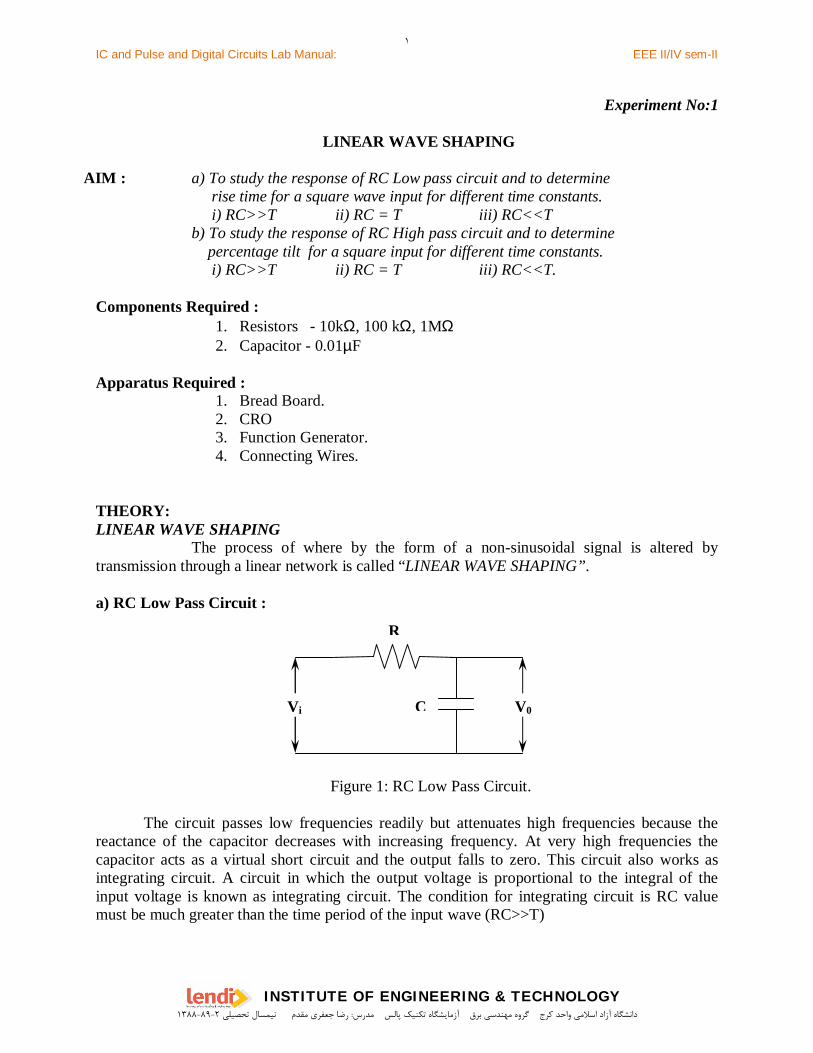
IC and Pulse and Digital Circuits Lab Manual: EEE II/IV sem-II
INSTITUTE OF ENGINEERING & TECHNOLOGY
Experiment No:1
LINEAR WAVE SHAPING
AIM : a) To study the response of RC Low pass circuit and to determinerise time for a square wave input for different time constants.
i) RC>>T ii) RC = T iii) RC<<Tb) To study the response of RC High pass circuit and to determine percentage tilt for a square input for different time constants.
i) RC>>T ii) RC = T iii) RC<<T.
Components Required :1. Resistors - 10kΩ, 100 kΩ, 1MΩ2. Capacitor - 0.01µF
Apparatus Required :1. Bread Board.2. CRO3. Function Generator.4. Connecting Wires.
THEORY:LINEAR WAVE SHAPING The process of where by the form of a non-sinusoidal signal is altered bytransmission through a linear network is called “LINEAR WAVE SHAPING”.
a) RC Low Pass Circuit :
Figure 1: RC Low Pass Circuit.
The circuit passes low frequencies readily but attenuates high frequencies because thereactance of the capacitor decreases with increasing frequency. At very high frequencies thecapacitor acts as a virtual short circuit and the output falls to zero. This circuit also works asintegrating circuit. A circuit in which the output voltage is proportional to the integral of theinput voltage is known as integrating circuit. The condition for integrating circuit is RC valuemust be much greater than the time period of the input wave (RC>>T)
V0
R
CVi
۱
دانشگاه آزاد اسالمي واحد كرج گروه مهندسي برق آزمايشگاه تكنيك پالس مدرس: رضا جعفري مقدم نيمسال تحصيلي 1۳۸۸-۸9-2
IC and Pulse and Digital Circuits Lab Manual: EEE II/IV sem-II
INSTITUTE OF ENGINEERING & TECHNOLOGY
Let Vi = alternating input voltage.i = resulting current
Applying Kirchoff’s Voltage Law to RC low pass circuit (fig.1).
∫+=T
oi dti
CiRV .1
Multiplying throughout by C, we get
∫+=T
oi dtiiRCCV .
As RC >> T, the term ∫T
o
dti. may be neglected
∴ iRCCVi =
Integrating with respect to T on both sides, we get
∫ ∫=T T
i dtiRCdtCV0 0
..
∫ ∫=T t
i dtVRC
dtiC 0 0
.1.1
∫=T
dtiC
V0
0 .1
∴ ∫=t
i dtVRC
V0
0 .1
The output voltage is proportional to the integral of the input voltage.
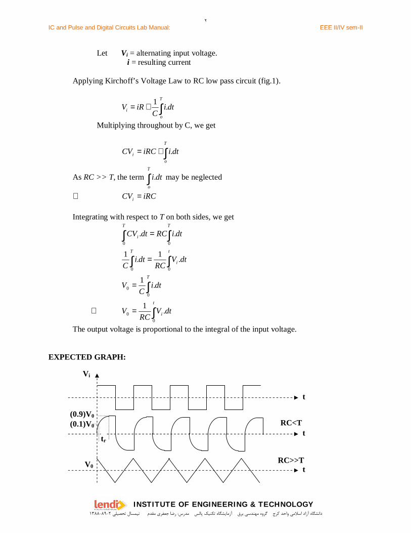
EXPECTED GRAPH:
Vi
t
t
t
RC<T
RC>>T
(0.9)V0
(0.1)V0
V0
tr
۲
دانشگاه آزاد اسالمي واحد كرج گروه مهندسي برق آزمايشگاه تكنيك پالس مدرس: رضا جعفري مقدم نيمسال تحصيلي 1۳۸۸-۸9-2
IC and Pulse and Digital Circuits Lab Manual: EEE II/IV sem-II
INSTITUTE OF ENGINEERING & TECHNOLOGY
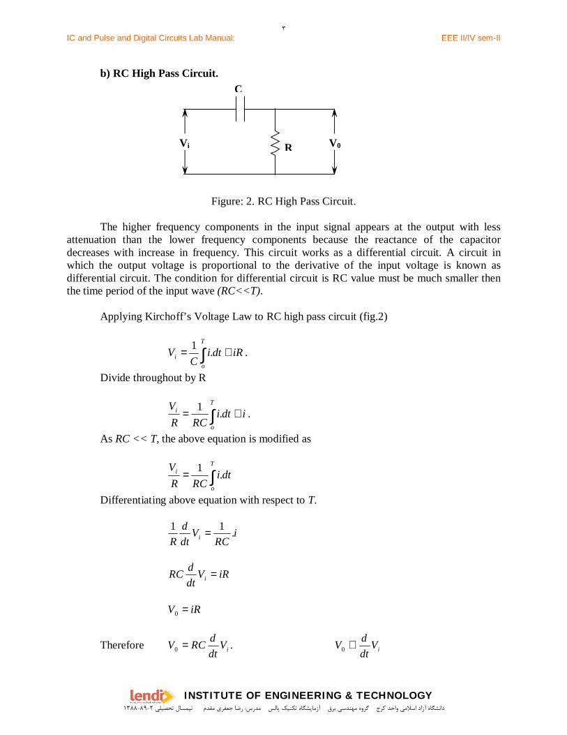
b) RC High Pass Circuit.
Figure: 2. RC High Pass Circuit.
The higher frequency components in the input signal appears at the output with lessattenuation than the lower frequency components because the reactance of the capacitordecreases with increase in frequency. This circuit works as a differential circuit. A circuit inwhich the output voltage is proportional to the derivative of the input voltage is known asdifferential circuit. The condition for differential circuit is RC value must be much smaller thenthe time period of the input wave (RC<<T).
Applying Kirchoff’s Voltage Law to RC high pass circuit (fig.2)
∫ +=T
oi iRdti
CV .1 .
Divide throughout by R
∫ +=T
o
i idtiRCR
V.1 .
As RC << T, the above equation is modified as
∫=T
o
i dtiRCR
V.1
Differentiating above equation with respect to T.
iRC
Vdtd
R i .11=
iRVdtdRC i =
iRV =0
Therefore iVdtdRCV =0 . iV
dtdV ∝0
C
R V0Vi
۳
دانشگاه آزاد اسالمي واحد كرج گروه مهندسي برق آزمايشگاه تكنيك پالس مدرس: رضا جعفري مقدم نيمسال تحصيلي 1۳۸۸-۸9-2
IC and Pulse and Digital Circuits Lab Manual: EEE II/IV sem-II
INSTITUTE OF ENGINEERING & TECHNOLOGY
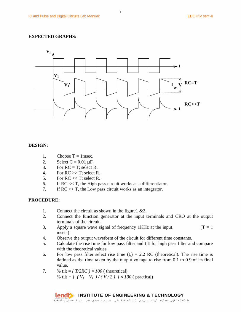
EXPECTED GRAPHS:
DESIGN:
1. Choose T = 1msec.2. Select C = 0.01 µF.3. For RC = T; select R.4. For RC >> T; select R.5. For RC << T; select R.6. If RC << T, the High pass circuit works as a differentiator.7. If RC >> T, the Low pass circuit works as an integrator.
PROCEDURE:
1. Connect the circuit as shown in the figure1 &2.2. Connect the function generator at the input terminals and CRO at the output
terminals of the circuit.3. Apply a square wave signal of frequency 1KHz at the input. (T = 1
msec.)4. Observe the output waveform of the circuit for different time constants.5. Calculate the rise time for low pass filter and tilt for high pass filter and compare
with the theoretical values.6. For low pass filter select rise time (tr) = 2.2 RC (theoretical). The rise time is
defined as the time taken by the output voltage to rise from 0.1 to 0.9 of its finalvalue.
7. % tilt = ( T/2RC ) × 100 ( theoretical)% tilt = [ ( V1 – V1′ ) / ( V / 2 ) ] × 100 ( practical)
Vi
t
t
t
RC=T
RC<<T
V1
V1′ V
۴
دانشگاه آزاد اسالمي واحد كرج گروه مهندسي برق آزمايشگاه تكنيك پالس مدرس: رضا جعفري مقدم نيمسال تحصيلي 1۳۸۸-۸9-2

IC and Pulse and Digital Circuits Lab Manual: EEE II/IV sem-II
INSTITUTE OF ENGINEERING & TECHNOLOGY
RESULT:1. Rise time for lowpass filter when RC <<T
Theoretical = Practical =2. % tilt for highpass filter when RC = T.
Theoretical = Practical =
Response of RC Low pass circuit is observed and rise time calculated.Response of RC High pass circuit is observed and percentage tilt iscalculated.
۵
دانشگاه آزاد اسالمي واحد كرج گروه مهندسي برق آزمايشگاه تكنيك پالس مدرس: رضا جعفري مقدم نيمسال تحصيلي 1۳۸۸-۸9-2
IC and Pulse and Digital Circuits Lab Manual: EEE II/IV sem-II
INSTITUTE OF ENGINEERING & TECHNOLOGY
Experiment No:2
NON LINEAR WAVE SHAPING - CLIPPERS
AIM : To study the clipping circuits for the following reference voltages andto verify the responses.
Components Required:1. Resistors - 1KΩ2. IN4007 Diode – 2No.
Apparatus Required :1. Bread board.2. Function generator3. CRO4. Power supply 0-30V5. Connecting wires.
THEORY:
The non-linear semiconductor diode in combination with resistor can function as clippercircuit. Energy storage circuit components are not required in the basic process of clipping.
These circuits will select part of an arbitrary waveform which lies above or below someparticular reference voltage level and that selected part of the waveform is used for transmission.So they are referred as voltage limiters, current limiters, amplitude selectors or slicers.
There are three different types of clipping circuits. 1) Positive Clipping circuit.
2) Negative Clipping.3) Positive and Negative Clipping ( slicer ).
In positive clipping circuit positive cycle of Sinusoidal signal is clipped and negativeportion of sinusoidal signal is obtained in the output of reference voltage is added, instead ofcomplete positive cycle that portion of the positive cycle which is above the reference voltagevalue is clipped. In negative clipping circuit instead of positive portion of sinusoidal signal, negativeportion is clipped. In slicer both positive and negative portions of the sinusoidal signal are clipped.
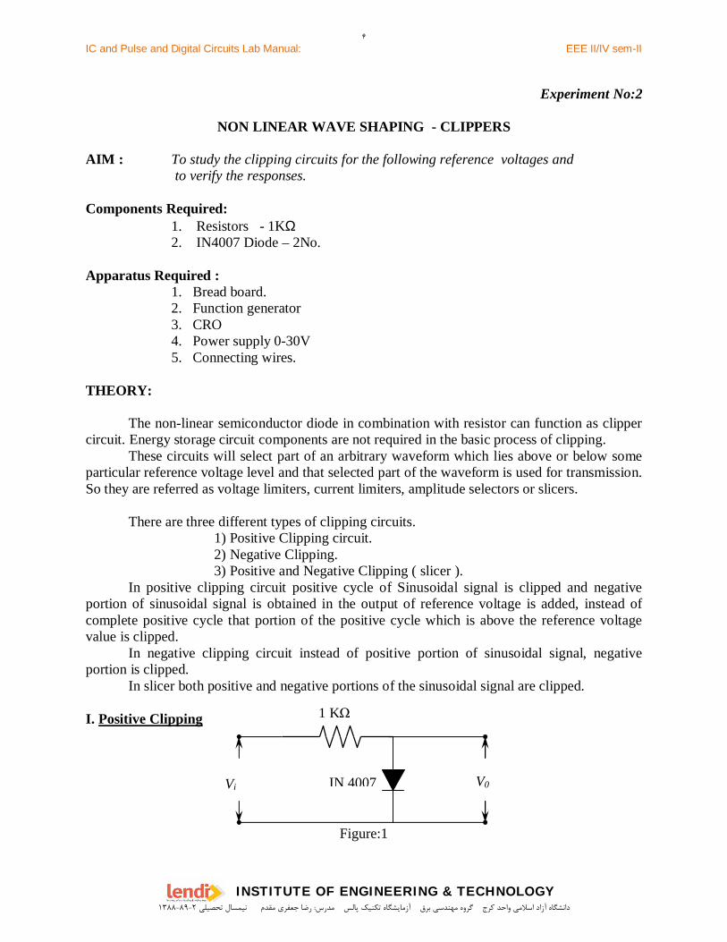
I. Positive Clipping
Figure:1
IN 4007
1 K
Vi V0
۶
دانشگاه آزاد اسالمي واحد كرج گروه مهندسي برق آزمايشگاه تكنيك پالس مدرس: رضا جعفري مقدم نيمسال تحصيلي 1۳۸۸-۸9-2
IC and Pulse and Digital Circuits Lab Manual: EEE II/IV sem-II
INSTITUTE OF ENGINEERING & TECHNOLOGY
Figure: 2(a). Input waveform Figure: 2(b)Output waveform.
Vi is a input sinusoidal signal as shown in the figure 2(a) . For positive portion of thesinusoidal the diode IN4007 gets forward biased. The output voltages in the voltage across thediode under forward biased which is cut-in-voltage of the diode. Therefore the positive portionabove the cut-in-voltage is clipped or not observed in the output (V0) as shown in figure 2(b).
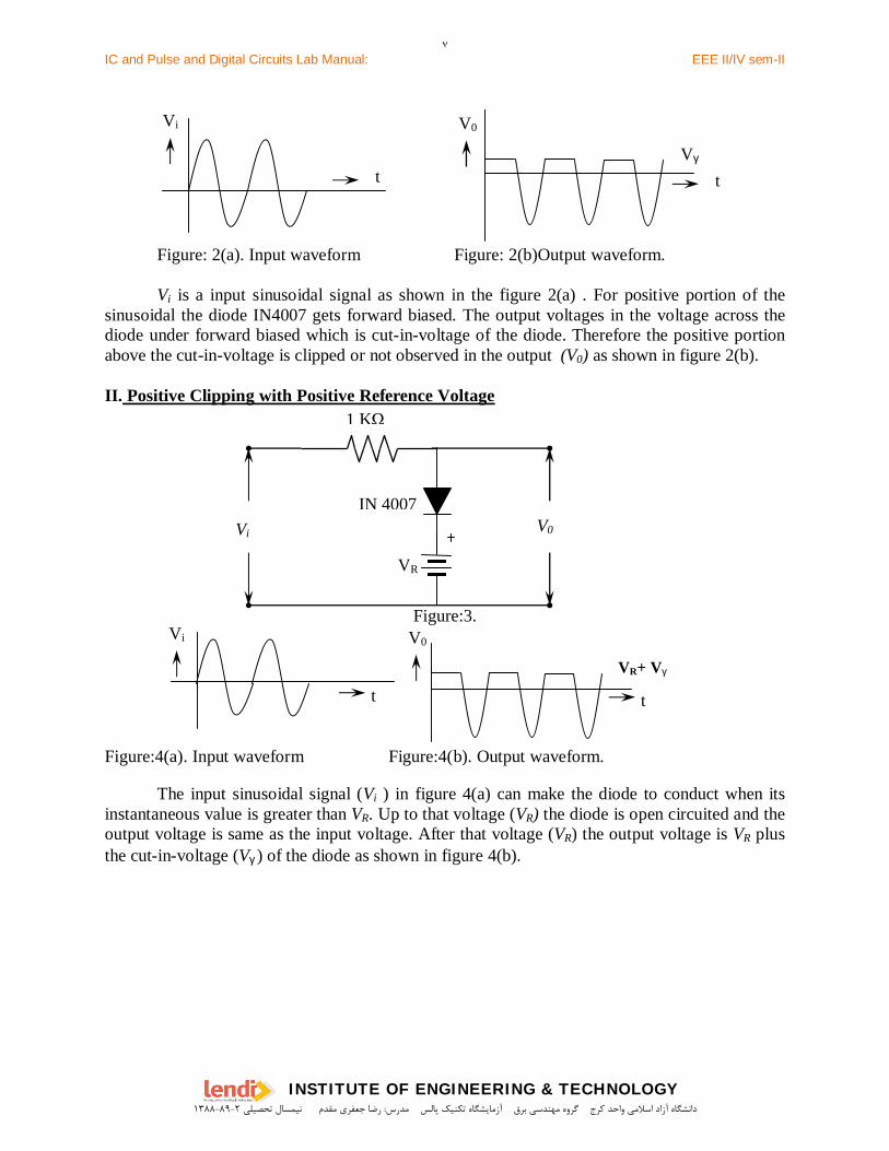
II. Positive Clipping with Positive Reference Voltage
Figure:3.
Figure:4(a). Input waveform Figure:4(b). Output waveform.
The input sinusoidal signal (Vi ) in figure 4(a) can make the diode to conduct when itsinstantaneous value is greater than VR. Up to that voltage (VR) the diode is open circuited and theoutput voltage is same as the input voltage. After that voltage (VR) the output voltage is VR plusthe cut-in-voltage (Vγ ) of the diode as shown in figure 4(b).
IN 4007
1 K
VR
Vi V0
Vi
tVγ
V0
t
Vi
tVR+ Vγ
V0
t
۷
دانشگاه آزاد اسالمي واحد كرج گروه مهندسي برق آزمايشگاه تكنيك پالس مدرس: رضا جعفري مقدم نيمسال تحصيلي 1۳۸۸-۸9-2
IC and Pulse and Digital Circuits Lab Manual: EEE II/IV sem-II
INSTITUTE OF ENGINEERING & TECHNOLOGY
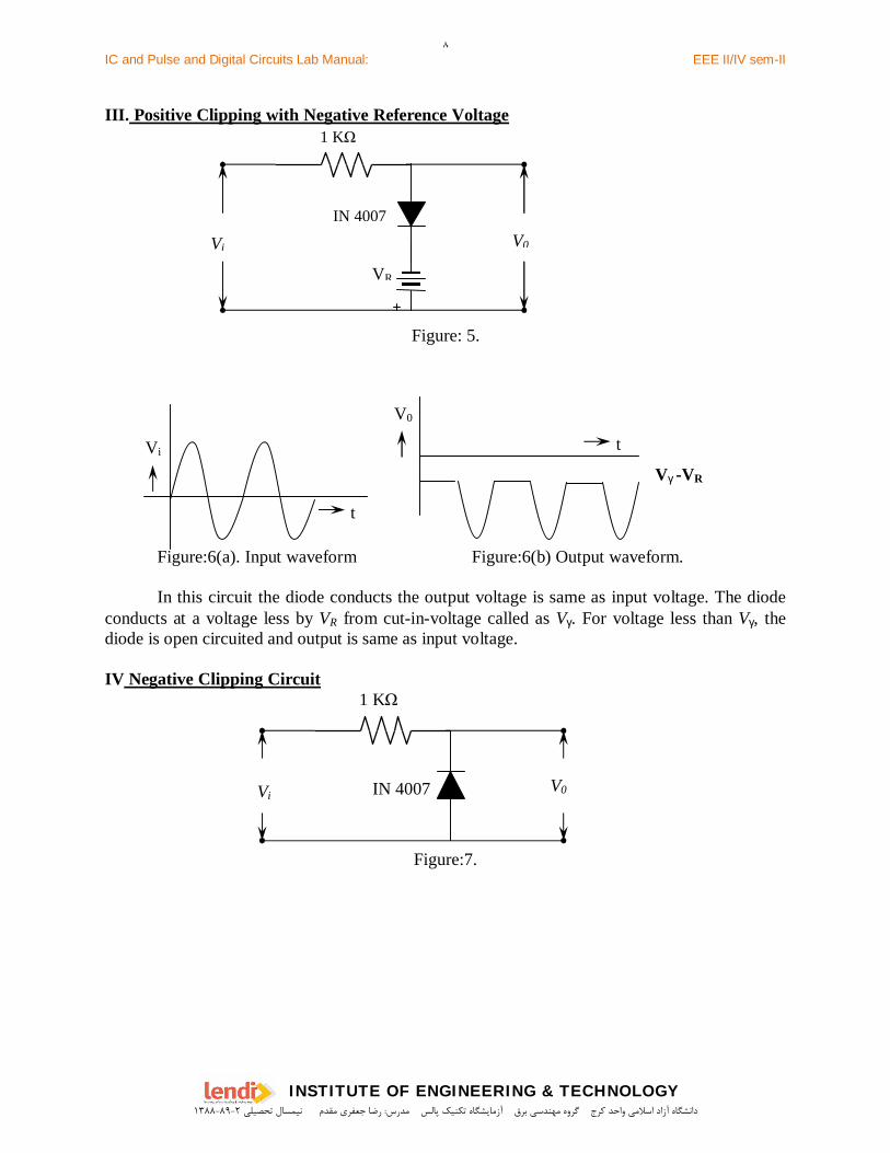
III. Positive Clipping with Negative Reference Voltage
Figure: 5.
Figure:6(a). Input waveform Figure:6(b) Output waveform.
In this circuit the diode conducts the output voltage is same as input voltage. The diodeconducts at a voltage less by VR from cut-in-voltage called as Vγ. For voltage less than Vγ, thediode is open circuited and output is same as input voltage.
IV Negative Clipping Circuit
Figure:7.
Vγ -VR
IN 4007
1 K
VR
Vi V0
IN 4007
1 K
ViV0
Vi
t
V0
t
۸
دانشگاه آزاد اسالمي واحد كرج گروه مهندسي برق آزمايشگاه تكنيك پالس مدرس: رضا جعفري مقدم نيمسال تحصيلي 1۳۸۸-۸9-2
IC and Pulse and Digital Circuits Lab Manual: EEE II/IV sem-II
INSTITUTE OF ENGINEERING & TECHNOLOGY
Figure:8 (a). Input waveform Figure:8 (b). Output waveform.
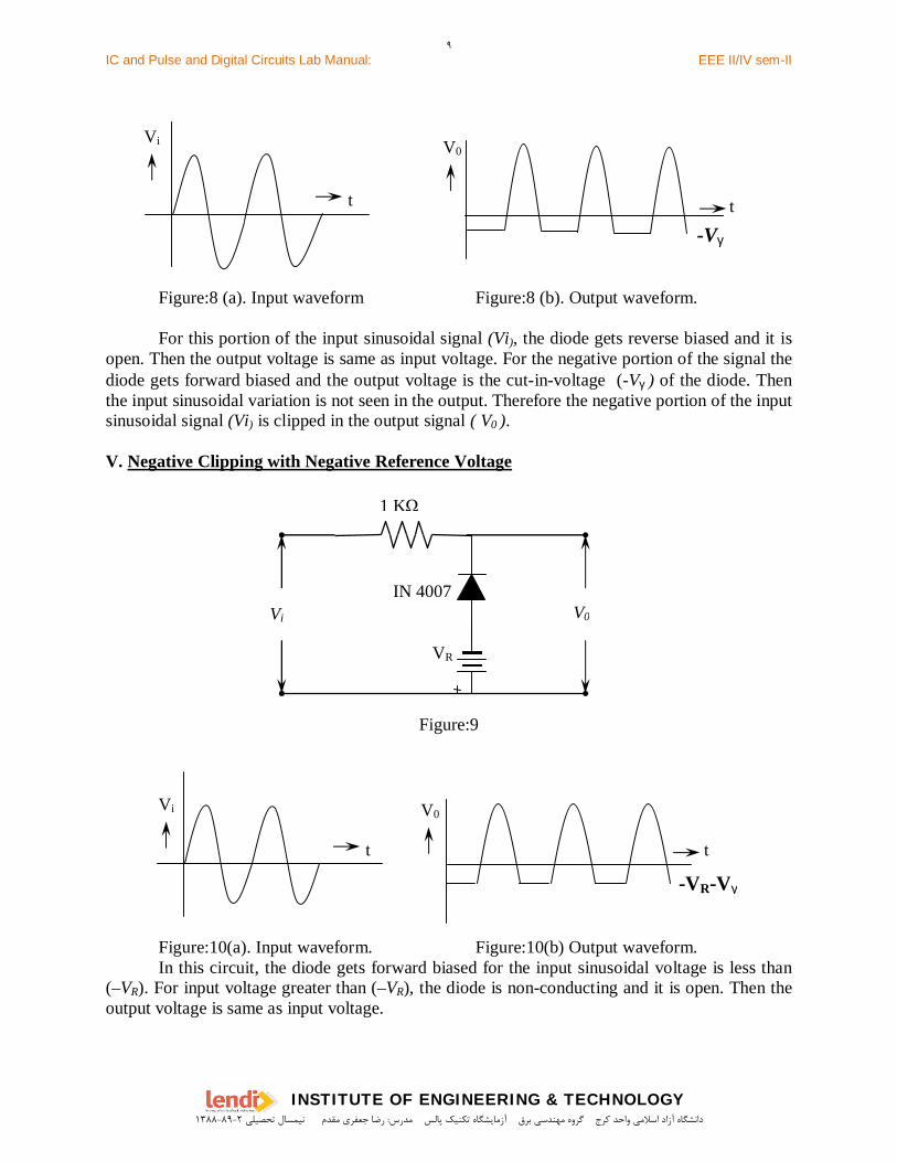
For this portion of the input sinusoidal signal (Vi), the diode gets reverse biased and it isopen. Then the output voltage is same as input voltage. For the negative portion of the signal thediode gets forward biased and the output voltage is the cut-in-voltage (-Vγ ) of the diode. Thenthe input sinusoidal variation is not seen in the output. Therefore the negative portion of the inputsinusoidal signal (Vi) is clipped in the output signal ( V0 ).
V. Negative Clipping with Negative Reference Voltage
Figure:9
Figure:10(a). Input waveform. Figure:10(b) Output waveform. In this circuit, the diode gets forward biased for the input sinusoidal voltage is less than(–VR). For input voltage greater than (–VR), the diode is non-conducting and it is open. Then theoutput voltage is same as input voltage.
IN 4007
1 K
VR
Vi V0
Vi
t
-Vγ
V0
t
Vi
t
-VR-Vγ
V0
t
۹
دانشگاه آزاد اسالمي واحد كرج گروه مهندسي برق آزمايشگاه تكنيك پالس مدرس: رضا جعفري مقدم نيمسال تحصيلي 1۳۸۸-۸9-2
IC and Pulse and Digital Circuits Lab Manual: EEE II/IV sem-II
INSTITUTE OF ENGINEERING & TECHNOLOGY
Vi V0
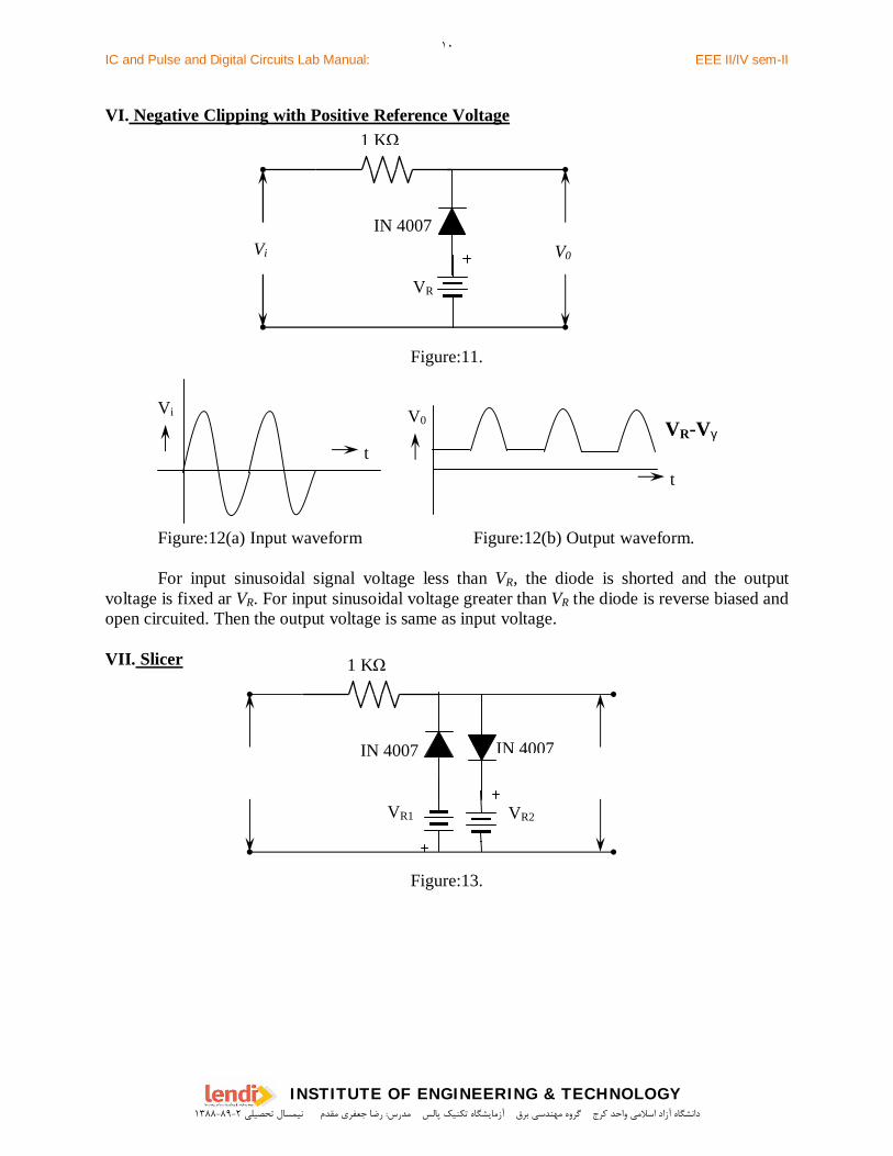
VI. Negative Clipping with Positive Reference Voltage
Figure:11.
Figure:12(a) Input waveform Figure:12(b) Output waveform.
For input sinusoidal signal voltage less than VR, the diode is shorted and the outputvoltage is fixed ar VR. For input sinusoidal voltage greater than VR the diode is reverse biased andopen circuited. Then the output voltage is same as input voltage.
VII. Slicer
Figure:13.
IN 4007
1 K
VR
IN 4007
1 K
VR1
IN 4007
VR2
Vi
tVR-Vγ
V0
t
۱۰
دانشگاه آزاد اسالمي واحد كرج گروه مهندسي برق آزمايشگاه تكنيك پالس مدرس: رضا جعفري مقدم نيمسال تحصيلي 1۳۸۸-۸9-2
IC and Pulse and Digital Circuits Lab Manual: EEE II/IV sem-II
INSTITUTE OF ENGINEERING & TECHNOLOGY
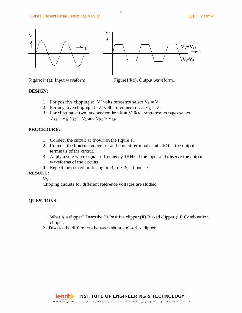
Figure:14(a). Input waveform Figure14(b). Output waveform.
DESIGN:
1. For positive clipping at ‘V’ volts reference select VR = V.2. For negative clipping at ‘V’ volts reference select VR = V.3. For clipping at two independent levels at V1&V2 reference voltages select VR1 = V1, VR2 = V2 and VR2 > VR1.
PROCEDURE:
1. Connect the circuit as shown in the figure 1.2. Connect the function generator at the input terminals and CRO at the output terminals of the circuit.3. Apply a sine wave signal of frequency 1KHz at the input and observe the output
waveforms of the circuits.4. Repeat the procedure for figure 3, 5, 7, 9, 11 and 13.
RESULT: Vγ = Clipping circuits for different reference voltages are studied.
QUESTIONS:
1. What is a clipper? Describe (i) Positive clipper (ii) Biased clipper (iii) Combinationclipper.
2. Discuss the differences between shunt and series clipper.
Vi
t Vγ+VR
Vγ-VR
V0
t
۱۱
دانشگاه آزاد اسالمي واحد كرج گروه مهندسي برق آزمايشگاه تكنيك پالس مدرس: رضا جعفري مقدم نيمسال تحصيلي 1۳۸۸-۸9-2

IC and Pulse and Digital Circuits Lab Manual: EEE II/IV sem-II
INSTITUTE OF ENGINEERING & TECHNOLOGY
Experiment No:3
NON LINEAR WAVE SHAPING – CLAMPERS
AIM : To get positive and negative clamping for sinusoidal and Square waveinputs.
Components Required:
1. Resistors - 1kΩ2. IN4007 Diode3. Capacitor -10µF
Apparatus Required:
1. Bread board2. Function generator3. CRO4. Power supply 0-30V5. Connecting Wires.
THEORY:
Clamping Circuit“A clamping circuit is one that takes an input waveform and provides an output that is
a faithful replica of its shape but has one edge tightly clamped to the zero voltage referencepoint”.
There are various types of Clamping circuits, which are mentioned below:
1. Positive Clamping Circuit.
2. Negative Clamping Circuit.
3. Positive Clamping with positive reference voltage.
4. Negative Clamping with positive reference voltage.
5. Positive Clamping with negative reference voltage.
6. Negative Clamping with negative reference voltage.
۱۲
دانشگاه آزاد اسالمي واحد كرج گروه مهندسي برق آزمايشگاه تكنيك پالس مدرس: رضا جعفري مقدم نيمسال تحصيلي 1۳۸۸-۸9-2
IC and Pulse and Digital Circuits Lab Manual: EEE II/IV sem-II
INSTITUTE OF ENGINEERING & TECHNOLOGY
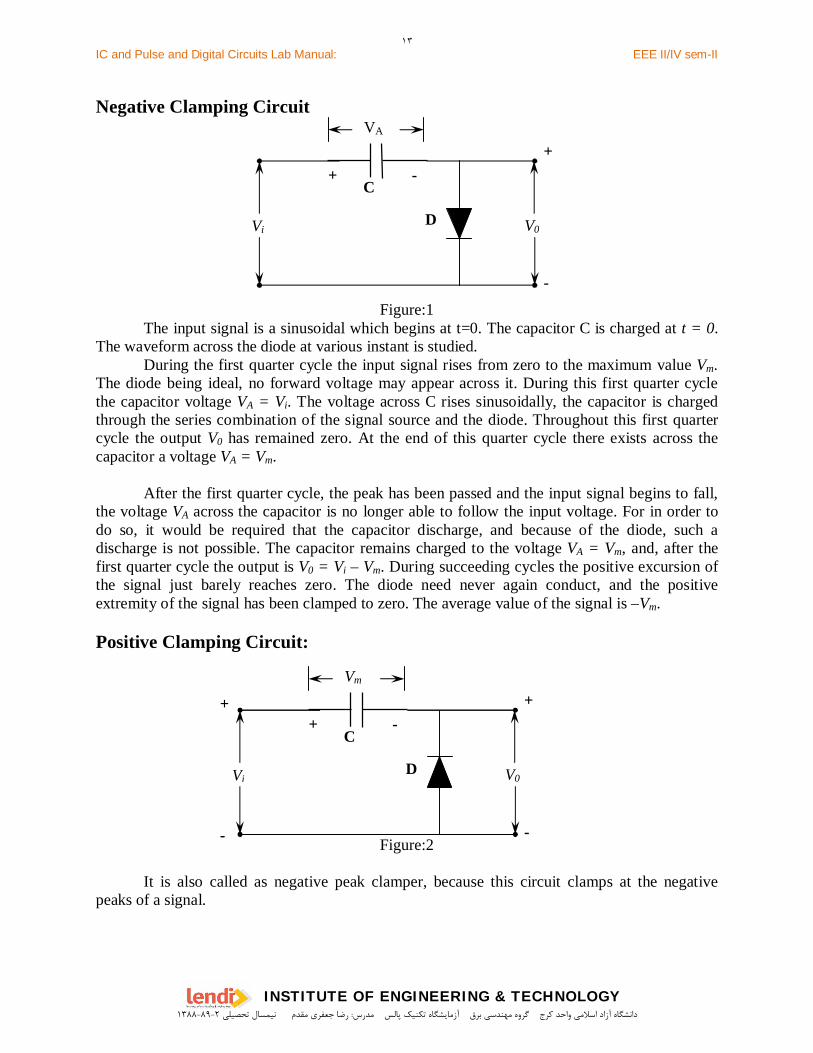
Negative Clamping Circuit
Figure:1 The input signal is a sinusoidal which begins at t=0. The capacitor C is charged at t = 0.The waveform across the diode at various instant is studied. During the first quarter cycle the input signal rises from zero to the maximum value Vm.The diode being ideal, no forward voltage may appear across it. During this first quarter cyclethe capacitor voltage VA = Vi. The voltage across C rises sinusoidally, the capacitor is chargedthrough the series combination of the signal source and the diode. Throughout this first quartercycle the output V0 has remained zero. At the end of this quarter cycle there exists across thecapacitor a voltage VA = Vm.
After the first quarter cycle, the peak has been passed and the input signal begins to fall,the voltage VA across the capacitor is no longer able to follow the input voltage. For in order todo so, it would be required that the capacitor discharge, and because of the diode, such adischarge is not possible. The capacitor remains charged to the voltage VA = Vm, and, after thefirst quarter cycle the output is V0 = Vi – Vm. During succeeding cycles the positive excursion ofthe signal just barely reaches zero. The diode need never again conduct, and the positiveextremity of the signal has been clamped to zero. The average value of the signal is –Vm.
Positive Clamping Circuit:
Figure:2
It is also called as negative peak clamper, because this circuit clamps at the negativepeaks of a signal.
Vi V0
VA
C
D
+ -+
-
Vi V0
Vm
C
D
+ -+
-
+
-
۱۳
دانشگاه آزاد اسالمي واحد كرج گروه مهندسي برق آزمايشگاه تكنيك پالس مدرس: رضا جعفري مقدم نيمسال تحصيلي 1۳۸۸-۸9-2
IC and Pulse and Digital Circuits Lab Manual: EEE II/IV sem-II
INSTITUTE OF ENGINEERING & TECHNOLOGY
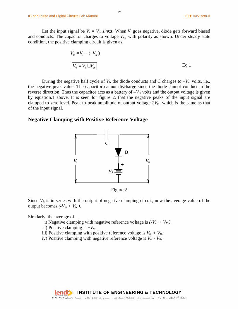
mi VVV +=0
Let the input signal be Vi = Vm sinωt. When Vi goes negative, diode gets forward biasedand conducts. The capacitor charges to voltage Vm, with polarity as shown. Under steady statecondition, the positive clamping circuit is given as,
)(0 mi VVV −−=
Eq.1
During the negative half cycle of Vi, the diode conducts and C charges to –Vm volts, i.e.,the negative peak value. The capacitor cannot discharge since the diode cannot conduct in thereverse direction. Thus the capacitor acts as a battery of –Vm volts and the output voltage is givenby equation.1 above. It is seen for figure 2, that the negative peaks of the input signal areclamped to zero level. Peak-to-peak amplitude of output voltage 2Vm, which is the same as thatof the input signal.
Negative Clamping with Positive Reference Voltage
Figure:2
Since VR is in series with the output of negative clamping circuit, now the average value of theoutput becomes (-Vm + VR ).
Similarly, the average of i) Negative clamping with negative reference voltage is (-Vm + VR ). ii) Positive clamping is +Vm. iii) Positive clamping with positive reference voltage is Vm + VR. iv) Positive clamping with negative reference voltage is Vm - VR.
Vi V0
C
D
VR
۱۴
دانشگاه آزاد اسالمي واحد كرج گروه مهندسي برق آزمايشگاه تكنيك پالس مدرس: رضا جعفري مقدم نيمسال تحصيلي 1۳۸۸-۸9-2
IC and Pulse and Digital Circuits Lab Manual: EEE II/IV sem-II
INSTITUTE OF ENGINEERING & TECHNOLOGY
Clamping Circuit Theorem:
It states that for any input waveform the ratio of the areas under the output voltage curvein forward direction to that in the reverse direction is equal to the ratio (Rf / R).
RR
AA f
r
f = .
Where Af = area of the output wave in forward direction.Ar = area of the output wave in reverse direction.Rf and R are forward and reverse resistances of the diode.
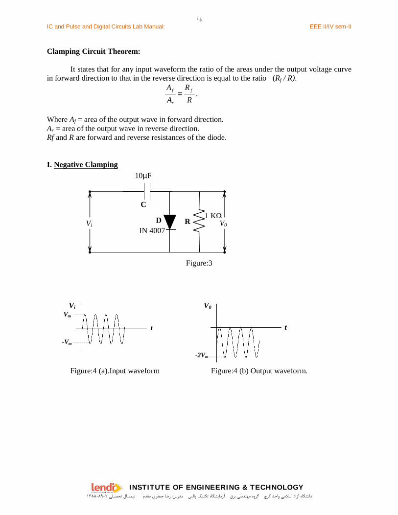
I. Negative Clamping
Figure:3
Figure:4 (a).Input waveform Figure:4 (b) Output waveform.
IN 4007
1 KVi V0
10µF
C
D R
Vi
t
Vm
-Vm
V0
t
-2Vm
۱۵
دانشگاه آزاد اسالمي واحد كرج گروه مهندسي برق آزمايشگاه تكنيك پالس مدرس: رضا جعفري مقدم نيمسال تحصيلي 1۳۸۸-۸9-2
IC and Pulse and Digital Circuits Lab Manual: EEE II/IV sem-II
INSTITUTE OF ENGINEERING & TECHNOLOGY
II. Negative Clamping with Positive Reference Voltage.
Figure:5
Figure:6 (a).Input waveform Figure:6 (b) Output waveform.
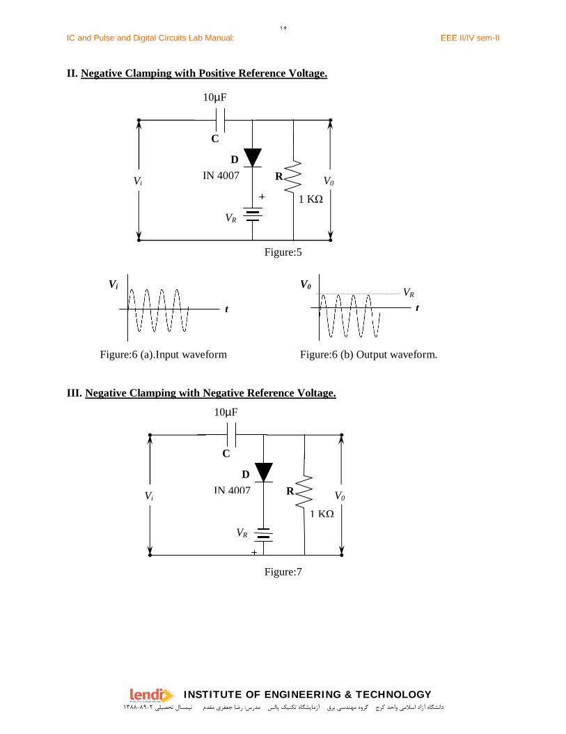
III. Negative Clamping with Negative Reference Voltage.
Figure:7
IN 4007
1 KVi V0
10µF
C
DR
VR
t
Vi VR
t
V0
IN 4007
1 K
Vi V0
10µF
C
DR
VR
۱۶
دانشگاه آزاد اسالمي واحد كرج گروه مهندسي برق آزمايشگاه تكنيك پالس مدرس: رضا جعفري مقدم نيمسال تحصيلي 1۳۸۸-۸9-2
IC and Pulse and Digital Circuits Lab Manual: EEE II/IV sem-II
INSTITUTE OF ENGINEERING & TECHNOLOGY
Figure:8 (a).Input waveform Figure:8 (b) Output waveform.
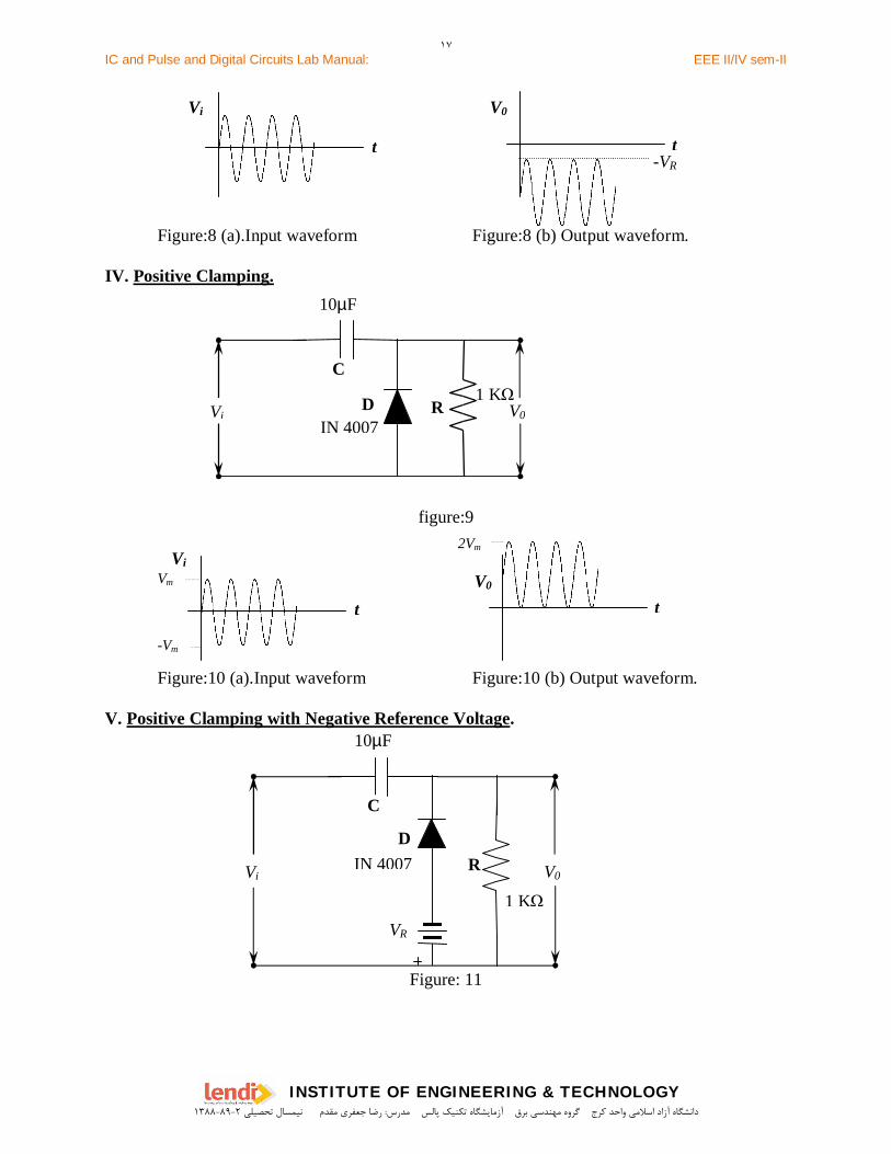
IV. Positive Clamping.
figure:9
Figure:10 (a).Input waveform Figure:10 (b) Output waveform.
V. Positive Clamping with Negative Reference Voltage.
Figure: 11
IN 4007
1 KVi V0
10µF
C
D R
IN 4007
1 K
Vi V0
10µF
C
DR
VR
tt
V0Vi
-VR
V0
t
Vi
t
2Vm
Vm
-Vm
۱۷
دانشگاه آزاد اسالمي واحد كرج گروه مهندسي برق آزمايشگاه تكنيك پالس مدرس: رضا جعفري مقدم نيمسال تحصيلي 1۳۸۸-۸9-2
IC and Pulse and Digital Circuits Lab Manual: EEE II/IV sem-II
INSTITUTE OF ENGINEERING & TECHNOLOGY
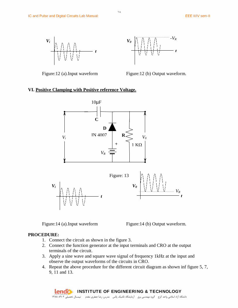
Figure:12 (a).Input waveform Figure:12 (b) Output waveform.
VI. Positive Clamping with Positive reference Voltage.
Figure: 13
Figure:14 (a).Input waveform Figure:14 (b) Output waveform.
PROCEDURE:1. Connect the circuit as shown in the figure 3.2. Connect the function generator at the input terminals and CRO at the output terminals of the circuit.3. Apply a sine wave and square wave signal of frequency 1kHz at the input and
observe the output waveforms of the circuits in CRO.4. Repeat the above procedure for the different circuit diagram as shown inf figure 5, 7,
9, 11 and 13.
IN 4007
1 KVi V0
10µF
C
DR
VR
t
ViVR
t
V0
t
Vi
t
V0-VR
۱۸
دانشگاه آزاد اسالمي واحد كرج گروه مهندسي برق آزمايشگاه تكنيك پالس مدرس: رضا جعفري مقدم نيمسال تحصيلي 1۳۸۸-۸9-2

IC and Pulse and Digital Circuits Lab Manual: EEE II/IV sem-II
INSTITUTE OF ENGINEERING & TECHNOLOGY
RESULT: The clamping voltages for positive and negative clamping circuits are noted.
QUESTIONS:1. Explain the operation of a clamping circuit for a square wave input.2. Differentiate the clippers with clampers.3. Give the applications of clampers.
۱۹
دانشگاه آزاد اسالمي واحد كرج گروه مهندسي برق آزمايشگاه تكنيك پالس مدرس: رضا جعفري مقدم نيمسال تحصيلي 1۳۸۸-۸9-2
IC and Pulse and Digital Circuits Lab Manual: EEE II/IV sem-II
INSTITUTE OF ENGINEERING & TECHNOLOGY
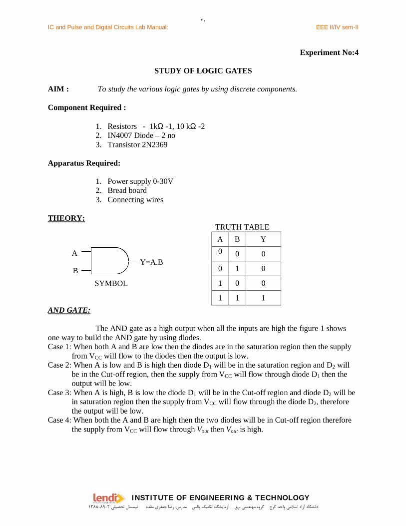
Experiment No:4
STUDY OF LOGIC GATES
AIM : To study the various logic gates by using discrete components.
Component Required :
1. Resistors - 1kΩ -1, 10 kΩ -22. IN4007 Diode – 2 no3. Transistor 2N2369
Apparatus Required:
1. Power supply 0-30V2. Bread board3. Connecting wires
THEORY: TRUTH TABLE
A B Y0 0 0
0 1 0
1 0 0
1 1 1AND GATE:
The AND gate as a high output when all the inputs are high the figure 1 showsone way to build the AND gate by using diodes.Case 1: When both A and B are low then the diodes are in the saturation region then the supply
from VCC will flow to the diodes then the output is low.Case 2: When A is low and B is high then diode D1 will be in the saturation region and D2 will
be in the Cut-off region, then the supply from VCC will flow through diode D1 then theoutput will be low.
Case 3: When A is high, B is low the diode D1 will be in the Cut-off region and diode D2 will bein saturation region then the supply from VCC will flow through the diode D2, thereforethe output will be low.
Case 4: When both the A and B are high then the two diodes will be in Cut-off region thereforethe supply from VCC will flow through Vout then Vout is high.
A
BY=A.B
SYMBOL
۲۰
دانشگاه آزاد اسالمي واحد كرج گروه مهندسي برق آزمايشگاه تكنيك پالس مدرس: رضا جعفري مقدم نيمسال تحصيلي 1۳۸۸-۸9-2

IC and Pulse and Digital Circuits Lab Manual: EEE II/IV sem-II
INSTITUTE OF ENGINEERING & TECHNOLOGY
OR GATE:
TRUTH TABLEA B Y0 0 0
0 1 1
1 0 1
1 1 1
An OR gate has two or more inputs but only one output signal. It is called OR gatebecause the output voltage is high if any or all the inputs are high. The figure 2 shows one way to build OR gate (two inputs) by using diodes.Case 1: When A and B are low then the two diodes D1 and D2 are in Cut-off region. Then the
Vout is low.Case 2: When A is low and B is high then the diode D1 is in Cut-off region and diode D2 is in
saturation region, then the Vout is high.Case 3: When A is high and B is low then the diode D2 is in saturation region and diode D1 is in
Cut-off region, then the Vout is high.Case 4: When both A and B are high the diodes D1 and D2 are in saturation region then the
output Vout is high.
NOR GATE: TRUTH TABLE
Symbol NOR gate is referred to a NOT OR gate because the output is BAY += . Read this as Y= NOT A OR B or Y = compliment of the A OR B. the circuit is in an OR gate followed by aNO gate OR inverter. The only to get high output is to have both inputs low.
A B Y
0 0 1
0 1 0
1 0 0
1 1 0
A
BY = A + B
SYMBOL
A
B
Y = A + B BAY +=
A
BBAY +=
۲۱
دانشگاه آزاد اسالمي واحد كرج گروه مهندسي برق آزمايشگاه تكنيك پالس مدرس: رضا جعفري مقدم نيمسال تحصيلي 1۳۸۸-۸9-2
IC and Pulse and Digital Circuits Lab Manual: EEE II/IV sem-II
INSTITUTE OF ENGINEERING & TECHNOLOGY
A
B
Y = A.B BAY .=
A
BBAY .=
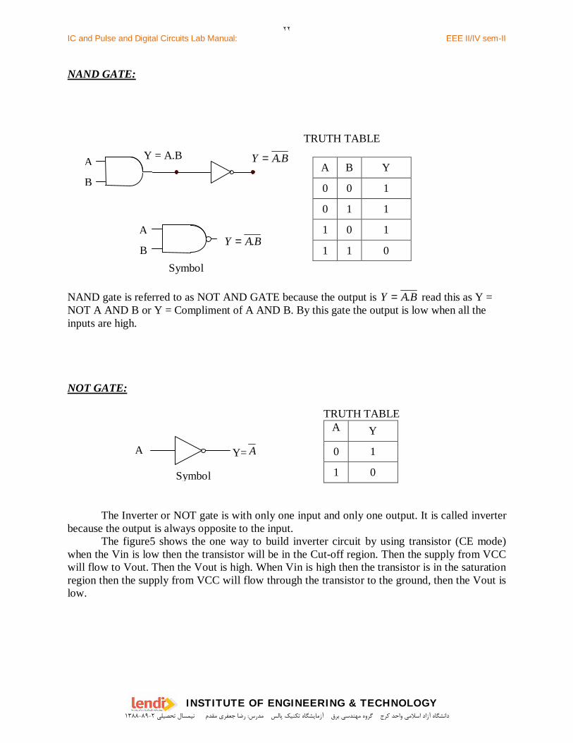
NAND GATE:
TRUTH TABLE
Symbol
NAND gate is referred to as NOT AND GATE because the output is BAY .= read this as Y =NOT A AND B or Y = Compliment of A AND B. By this gate the output is low when all theinputs are high.
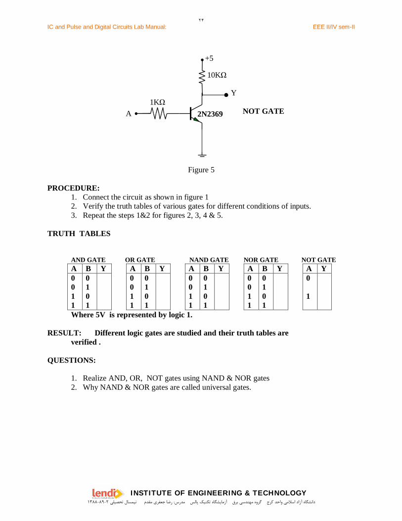
NOT GATE:
TRUTH TABLEA Y
0 1
1 0
The Inverter or NOT gate is with only one input and only one output. It is called inverterbecause the output is always opposite to the input. The figure5 shows the one way to build inverter circuit by using transistor (CE mode)when the Vin is low then the transistor will be in the Cut-off region. Then the supply from VCCwill flow to Vout. Then the Vout is high. When Vin is high then the transistor is in the saturationregion then the supply from VCC will flow through the transistor to the ground, then the Vout islow.
A B Y
0 0 1
0 1 1
1 0 1
1 1 0
A Y= A
Symbol
۲۲
دانشگاه آزاد اسالمي واحد كرج گروه مهندسي برق آزمايشگاه تكنيك پالس مدرس: رضا جعفري مقدم نيمسال تحصيلي 1۳۸۸-۸9-2
IC and Pulse and Digital Circuits Lab Manual: EEE II/IV sem-II
INSTITUTE OF ENGINEERING & TECHNOLOGY
CIRCUIT DIAGRAM :
Figure 1 Figure 2
Figure 3
Figure 4
D1 IN4007
D2 IN4007
10K
YA
B
+5AND GATE
D1 IN4007
D2 IN4007
10K
YA
B
+5OR GATE
D1 IN4007
D2 IN4007
10K
Y
A
B
+5
NOR GATE
1K
10K
2N2369
D1 IN4007
D2 IN4007
10KY
A
B
VCC +5V
NAND GATE
1K
10K
2N2369
۲۳
دانشگاه آزاد اسالمي واحد كرج گروه مهندسي برق آزمايشگاه تكنيك پالس مدرس: رضا جعفري مقدم نيمسال تحصيلي 1۳۸۸-۸9-2
IC and Pulse and Digital Circuits Lab Manual: EEE II/IV sem-II
INSTITUTE OF ENGINEERING & TECHNOLOGY
Figure 5
PROCEDURE:1. Connect the circuit as shown in figure 12. Verify the truth tables of various gates for different conditions of inputs.3. Repeat the steps 1&2 for figures 2, 3, 4 & 5.
TRUTH TABLES
AND GATE OR GATE NAND GATE NOR GATE NOT GATEA B Y A B Y A B Y A B Y A Y0011
0101
0011
0101
0011
0101
0011
0101
0
1
Where 5V is represented by logic 1.
RESULT: Different logic gates are studied and their truth tables areverified .
QUESTIONS:
1. Realize AND, OR, NOT gates using NAND & NOR gates2. Why NAND & NOR gates are called universal gates.
+5
1KY
2N2369A NOT GATE
10K
۲۴
دانشگاه آزاد اسالمي واحد كرج گروه مهندسي برق آزمايشگاه تكنيك پالس مدرس: رضا جعفري مقدم نيمسال تحصيلي 1۳۸۸-۸9-2
IC and Pulse and Digital Circuits Lab Manual: EEE II/IV sem-II
INSTITUTE OF ENGINEERING & TECHNOLOGY
Experiment No:5
ASTABLE MULTIVIBRATOR
AIM : a) To design and test performance of an Astable Multivibrator to generate clock pulse for a given frequency.
COMPONENTS REQUIRED:1. Resistors2. Capacitors 0.1 µf - 23. Transistors 2N2369 – 2
APPARATUS :1. CRO2. Power supply 0-30V3. Bread board4. Connecting wires
THEORY:An Astable multivibrator has two quasi-stable states, and it keeps on switching between
these two states, by itself, No external triggering signal is needed. The astable multivibratorcannot remain indefinitely in any of these two states. The two amplifiers of an astablemultivibrator are regeneratively cross-coupled by capacitor.
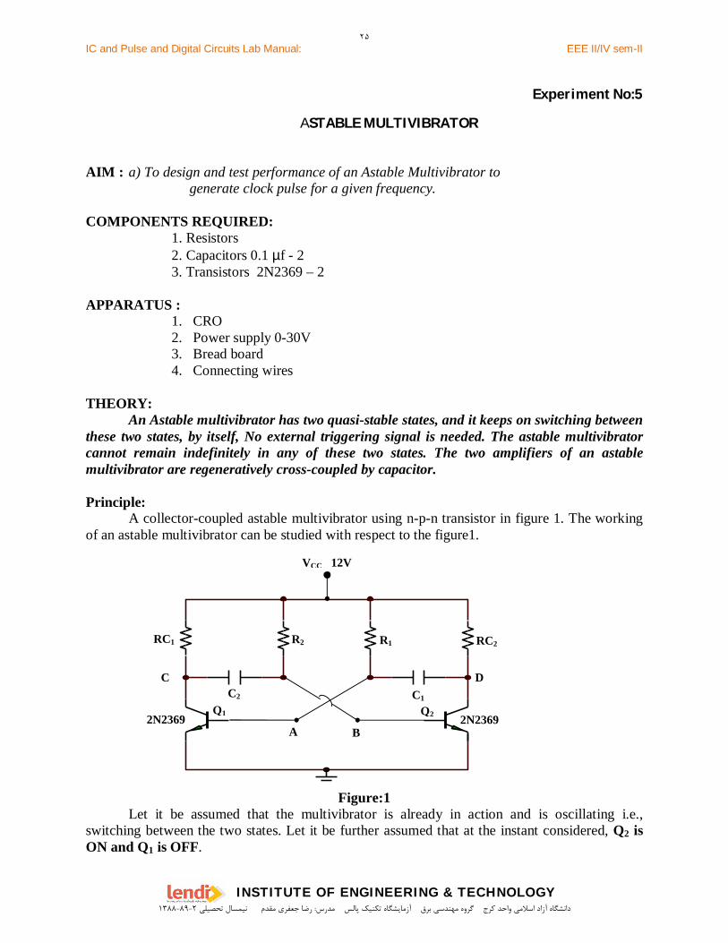
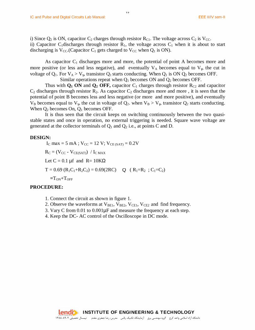
Principle: A collector-coupled astable multivibrator using n-p-n transistor in figure 1. The workingof an astable multivibrator can be studied with respect to the figure1.
Figure:1 Let it be assumed that the multivibrator is already in action and is oscillating i.e.,switching between the two states. Let it be further assumed that at the instant considered, Q2 isON and Q1 is OFF.
RC1 RC2R2 R1
C2 C1
2N23692N2369
VCC 12V
Q1 Q2
A B
C D
۲۵
دانشگاه آزاد اسالمي واحد كرج گروه مهندسي برق آزمايشگاه تكنيك پالس مدرس: رضا جعفري مقدم نيمسال تحصيلي 1۳۸۸-۸9-2
IC and Pulse and Digital Circuits Lab Manual: EEE II/IV sem-II
INSTITUTE OF ENGINEERING & TECHNOLOGY
i) Since Q2 is ON, capacitor C2 charges through resistor RC1. The voltage across C2 is VCC.ii) Capacitor C1discharges through resistor R1, the voltage across C1 when it is about to startdischarging is VCC.(Capacitor C1 gets charged to VCC when Q1 is ON).
As capacitor C1 discharges more and more, the potential of point A becomes more andmore positive (or less and less negative), and eventually VA becomes equal to Vγ, the cut involtage of Q1. For VA > Vγ, transistor Q1 starts conducting. When Q1 is ON Q2 becomes OFF. Similar operations repeat when Q1 becomes ON and Q2 becomes OFF. Thus with Q1 ON and Q2 OFF, capacitor C1 charges through resistor RC2 and capacitorC2 discharges through resistor R2. As capacitor C2 discharges more and more , it is seen that thepotential of point B becomes less and less negative (or more and more positive), and eventuallyVB becomes equal to Vγ, the cut in voltage of Q2. when VB > Vγ, transistor Q2 starts conducting.When Q2 becomes On, Q1 becomes OFF. It is thus seen that the circuit keeps on switching continuously between the two quasi-stable states and once in operation, no external triggering is needed. Square wave voltage aregenerated at the collector terminals of Q1 and Q2 i.e., at points C and D.
DESIGN: IC max = 5 mA ; VCC = 12 V; VCE (SAT) = 0.2V
RC = (VCC - VCE(SAT)) / IC MAX
Let C = 0.1 µf and R= 10KΩ
T = 0.69 (R1C1+R2C2) = 0.69(2RC) ( R1=R2 ; C1=C2)
=TON+TOFF
PROCEDURE:
1. Connect the circuit as shown in figure 1.2. Observe the waveforms at VBE1, VBE2, VCE1, VCE2 and find frequency.3. Vary C from 0.01 to 0.001µF and measure the frequency at each step.4. Keep the DC- AC control of the Oscilloscope in DC mode.
Q
۲۶
دانشگاه آزاد اسالمي واحد كرج گروه مهندسي برق آزمايشگاه تكنيك پالس مدرس: رضا جعفري مقدم نيمسال تحصيلي 1۳۸۸-۸9-2
IC and Pulse and Digital Circuits Lab Manual: EEE II/IV sem-II
INSTITUTE OF ENGINEERING & TECHNOLOGY
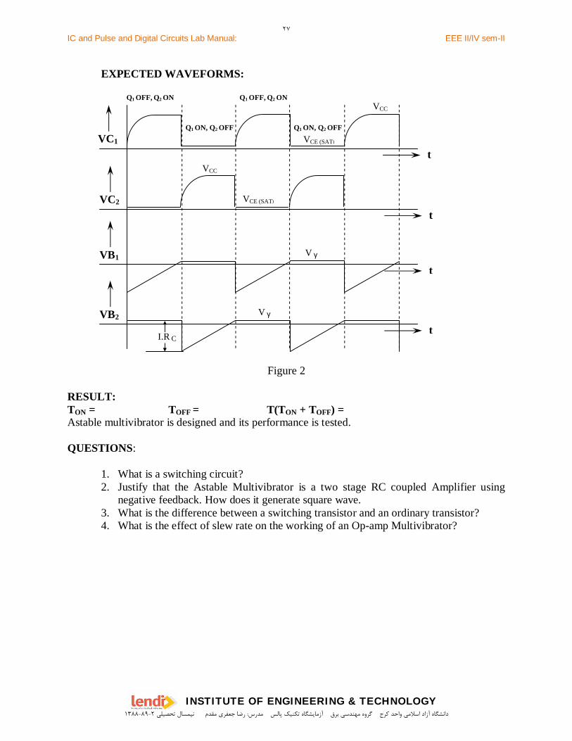
EXPECTED WAVEFORMS:
Q1 OFF, Q2 ON Q1 OFF, Q2 ON
Q1 ON, Q2 OFF Q1 ON, Q2 OFF
Figure 2
RESULT:TON = TOFF = T(TON + TOFF) =Astable multivibrator is designed and its performance is tested.
QUESTIONS:
1. What is a switching circuit?2. Justify that the Astable Multivibrator is a two stage RC coupled Amplifier using
negative feedback. How does it generate square wave.3. What is the difference between a switching transistor and an ordinary transistor?4. What is the effect of slew rate on the working of an Op-amp Multivibrator?
VC1
t
VC2
t
VB1
t
VB2
t
VCE (SAT)
VCE (SAT)
VCC
V γ
V γ
VCC
I.R C
۲۷
دانشگاه آزاد اسالمي واحد كرج گروه مهندسي برق آزمايشگاه تكنيك پالس مدرس: رضا جعفري مقدم نيمسال تحصيلي 1۳۸۸-۸9-2
IC and Pulse and Digital Circuits Lab Manual: EEE II/IV sem-II
INSTITUTE OF ENGINEERING & TECHNOLOGY
Experiment No:6
MONOSTABLE MULTIVIBRATOR
AIM : a) To design and test performance of a monostable multivibrator to generate clockpulse for a given frequency. And obtain the waveforms.
Components Required:1. Resistors2. Capacitors.3. Transistors 2N2369 – 2
Apparatus Required:1. CRO2. Power supply 0-30V3. Bread board4. Connecting wires
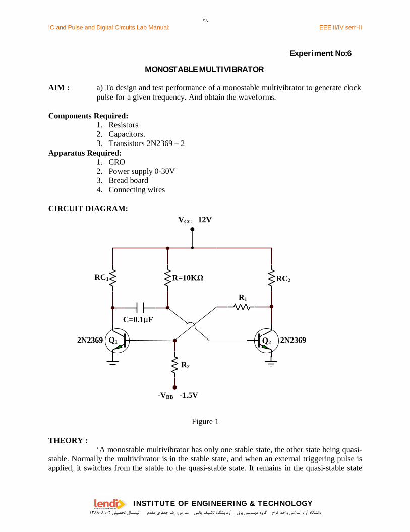
CIRCUIT DIAGRAM:
Figure 1
THEORY :‘A monostable multivibrator has only one stable state, the other state being quasi-
stable. Normally the multivibrator is in the stable state, and when an external triggering pulse isapplied, it switches from the stable to the quasi-stable state. It remains in the quasi-stable state
RC1 RC2R=10K
R1
C=0.1µF
2N23692N2369
VCC 12V
-VBB -1.5V
R2
Q1 Q2
۲۸
دانشگاه آزاد اسالمي واحد كرج گروه مهندسي برق آزمايشگاه تكنيك پالس مدرس: رضا جعفري مقدم نيمسال تحصيلي 1۳۸۸-۸9-2
IC and Pulse and Digital Circuits Lab Manual: EEE II/IV sem-II
INSTITUTE OF ENGINEERING & TECHNOLOGY
fro a short duration, but automatically reverts i.e. switches back to its original stable state,without any triggering pulse’.
Principle of operation A collector-coupled Monostable multivibrator of the two transistors Q1 and Q2, Q1 isnormally OFF and Q2 is Normally ON. Resistor R1 and R2 are connected to the normally OFFtransistor, and the capacitor C is connected to the normally ON transistor. It is seen from the circuit of the monostable multivibrator that, under normal conditions,the supply voltage VCC provides enough base drive to the transistor Q2 through resistor R, withthe result that Q2 goes into saturation. With Q2 ON, Q1 goes OFF, as already studied in thecontext of binary operation. With Q2 ON and Q1 OFF, the capacitor finds a charging path. The voltage across thecapacitor is VCC with polarity. It is obvious that in the stable state of the multivibrator, Q2 is ONand Q1 is OFF. If the negative triggering pulse is applied to the collector of Q1, it is transmitted to thebase of Q2 through the capacitor, and hence makes the base of Q2 negative. Immediately Q2 goesOFF and Q1 becomes ON. However, this is only a quasi-stable state as is obvious form thefollowing observation. With Q1 ON and Q2 OFF, the capacitor C finds a discharging path. As the capacitordischarges, it is seen that the potential at the base of the transistor Q2 becomes less and lessnegative, and after a time, we have VB = Vγ, the cut-in-voltage of Q2. As soon as VB crosses the level of Vγ, Q2 starts conducting and gets saturated.When Q2 becomes ON, Q1 becomes OFF. Thus the original stable state of the multivibrator isrestored.
[ In quasi-stable state: Q1 is ON and Q2 is OFF] The interval during which the quasi-stable state of the multivibrator persists i.e., Q2remains OFF is dependent upon the rate at which the capacitor C discharges. This duration of thequasi-stable state is termed as delay time or pulse width or gate time. It is denoted as T. Thewave forms of the voltage at base of the transistor Q2 and C (Collector of Q1)
DESIGN:VCE = 5.56v, VCC = 6v, VCE(sat) = 0.3v, VBE(sat), = 0.7v, IC = 6mA,VF = -0.3vRc = (VCC–VCE(sat))/IC.
C
CsatBE
C
CCCE RR
RVRRRVV
++
+=
1
)(
1
1
Find the values of R1 and R2PROCEDURE:
1. Connect the circuit as shown in figure.2. With the help of a triggering circuit and using the condition T (trig) > T(Quasi) a pulse waveform is generated.
3. The output of the triggering circuit is connected to the base of the off transistor. 4. The Off transistor goes into ON state.
5. Observe the waveforms at VBE1, VBE2, VCE1, VCE26. Keep the DC- AC control of the Oscilloscope in DC mode.
21
2)(
21
1
RRRV
RRRVV satCEBB
F ++
+−
=
۲۹
دانشگاه آزاد اسالمي واحد كرج گروه مهندسي برق آزمايشگاه تكنيك پالس مدرس: رضا جعفري مقدم نيمسال تحصيلي 1۳۸۸-۸9-2
IC and Pulse and Digital Circuits Lab Manual: EEE II/IV sem-II
INSTITUTE OF ENGINEERING & TECHNOLOGY
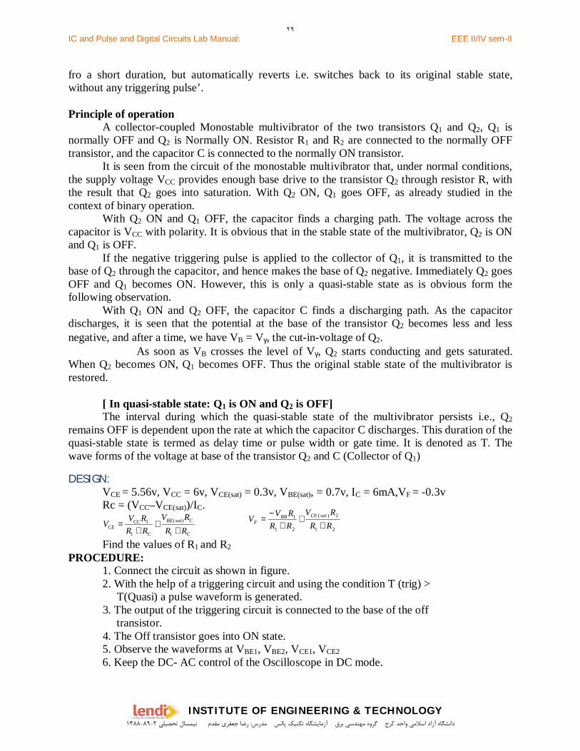
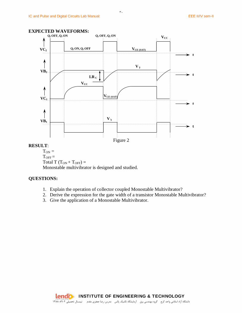
EXPECTED WAVEFORMS: Q2 OFF, Q1 ON Q1 OFF, Q2 ON
Q2 ON, Q1 OFF
Figure 2RESULT: TON = TOFF = Total T (TON + TOFF) =
Monostable multivibrator is designed and studied.
QUESTIONS:
1. Explain the operation of collector coupled Monostable Multivibrator?2. Derive the expression for the gate width of a transistor Monostable Multivibrator?3. Give the application of a Monostable Multivibrator.
VC2
t
VB2t
VC1
t
VB1
t
VCE (SAT)
VCE (SAT)
VCC
V γ
V γ
VCC
I.R C
۳۰
دانشگاه آزاد اسالمي واحد كرج گروه مهندسي برق آزمايشگاه تكنيك پالس مدرس: رضا جعفري مقدم نيمسال تحصيلي 1۳۸۸-۸9-2
IC and Pulse and Digital Circuits Lab Manual: EEE II/IV sem-II
INSTITUTE OF ENGINEERING & TECHNOLOGY
Experiment No:7
BISTABLE MULTIVIBRATOR
AIM: To design a fixed bias Bistable Multivibrator and to measure the stable statevoltages and after triggering.
COMPONENTS REQUIRED:1. Resistors2. Capacitors.3. Transistors 2N2369 – 2
APPARATUS:1. Bread board2. Power supply 0-30V3. CRO4. Connecting wires
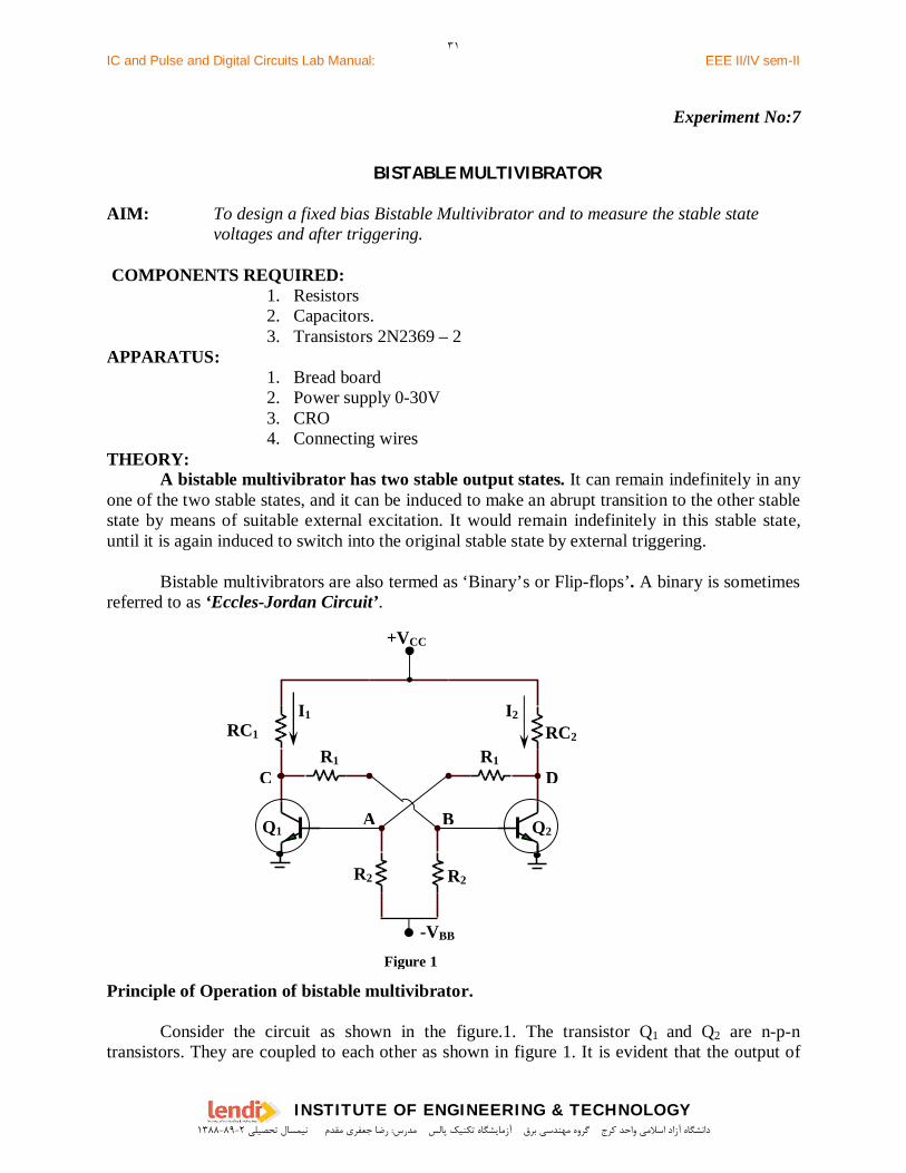
THEORY:A bistable multivibrator has two stable output states. It can remain indefinitely in any
one of the two stable states, and it can be induced to make an abrupt transition to the other stablestate by means of suitable external excitation. It would remain indefinitely in this stable state,until it is again induced to switch into the original stable state by external triggering.
Bistable multivibrators are also termed as ‘Binary’s or Flip-flops’. A binary is sometimesreferred to as ‘Eccles-Jordan Circuit’.
Principle of Operation of bistable multivibrator.
Consider the circuit as shown in the figure.1. The transistor Q1 and Q2 are n-p-ntransistors. They are coupled to each other as shown in figure 1. It is evident that the output of
RC1 RC2
R1
Q2
+VCC
Q1
R2 R2
R1
-VBB
A B
C D
I1 I2
Figure 1
۳۱
دانشگاه آزاد اسالمي واحد كرج گروه مهندسي برق آزمايشگاه تكنيك پالس مدرس: رضا جعفري مقدم نيمسال تحصيلي 1۳۸۸-۸9-2
IC and Pulse and Digital Circuits Lab Manual: EEE II/IV sem-II
INSTITUTE OF ENGINEERING & TECHNOLOGY
each transistor is coupled to the input of the other transistor. Since the transistors are identical,there quiescent currents would be the same, unless the loop gain is greater than unity. When I1increases slightly, the voltage drop across the collector resistance RC1 increases. Since VCC isfixed, the voltage of point C decreases. This has the effect of decreasing the base current of Q2.This, in turn, decreases the collector current of Q2 viz. I2 decreases, the voltage drop I2RC2decreases. Hence the voltage of point D increases. Due to increase of VD, the base current of Q1 increases. This increases the collectorcurrent of Q1 viz I1. Thus I1 further increases. I1RC1 drop further increases, VC further decreases,the base current of Q2 further decreases, with the result that I2 further decreases. Thus it caneasily seen that if the collector current I1 increases even marginally, I2 would go on progressivelydecreasing and as a result, I1 would progressively increase. Eventually I2 would becomepractically zero, cutting off the transistor Q2, at the same time transistor Q1 would conductheavily with the result that it would be driven into saturation. Thus Q2 becomes OFF and Q1becomes ON. It can similarly be shown that if I2 increases even marginally similar sequence ofoperation would result and ultimately Q2 would be ON and Q1 OFF. Thus when Q1 is ON, Q2 isOFF and when Q1 is OFF Q2 is ON.
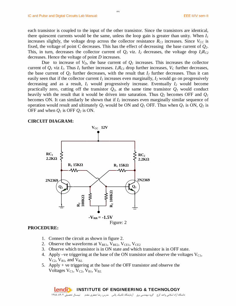
CIRCUIT DIAGRAM:
Figure: 2PROCEDURE:
1. Connect the circuit as shown in figure 2.2. Observe the waveforms at VBE1, VBE2, VCE1, VCE23. Observe which transistor is in ON state and which transistor is in OFF state.4. Apply –ve triggering at the base of the ON transistor and observe the voltages VC1,
VC2, VB1, and VB2.5. Apply + ve triggering at the base of the OFF transistor and observe the
Voltages VC1, VC2, VB1, VB2.
RC12.2K
RC22.2K
R1 15K
2N23692N2369
VCC 12V
-VBB = -1.5V
R1 15K
R2
100K
R2
100K
Q1Q2
۳۲
دانشگاه آزاد اسالمي واحد كرج گروه مهندسي برق آزمايشگاه تكنيك پالس مدرس: رضا جعفري مقدم نيمسال تحصيلي 1۳۸۸-۸9-2

IC and Pulse and Digital Circuits Lab Manual: EEE II/IV sem-II
INSTITUTE OF ENGINEERING & TECHNOLOGY
EXPECTED WAVEFORMS:
RESULT:
QUESTIONS:1. What is Multivibrator? Explain the principle on which it works? Why is it called a
binary?2. Explain the role of commutating capacitors in a Bistable Multivibrator?3. Give the Application of a Binary.
VBE1 VBE2 VCE1 VCE2Stable state Voltages
t
Vol
tage VC1
VC2
Before Triggeringt
Vol
tage
VC1
VC2
After Triggering0 0
۳۳
دانشگاه آزاد اسالمي واحد كرج گروه مهندسي برق آزمايشگاه تكنيك پالس مدرس: رضا جعفري مقدم نيمسال تحصيلي 1۳۸۸-۸9-2
IC and Pulse and Digital Circuits Lab Manual: EEE II/IV sem-II
INSTITUTE OF ENGINEERING & TECHNOLOGY
Experiment No: 8
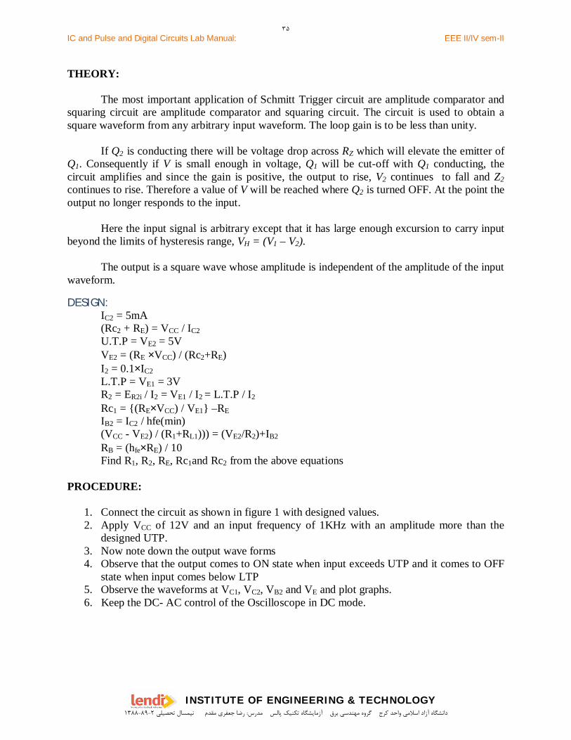
SCHMITT TRIGGER
AIM: To design and analyze Schmitt trigger and to observe the waveforms.
COMPONENTS REQUIRED:1. Resistors2. Transistors 2N2369 – 23.
APPARATUS:1. Bread board2. Power supply 0-30V3. Signal generator4. CRO5. Connecting Wires.
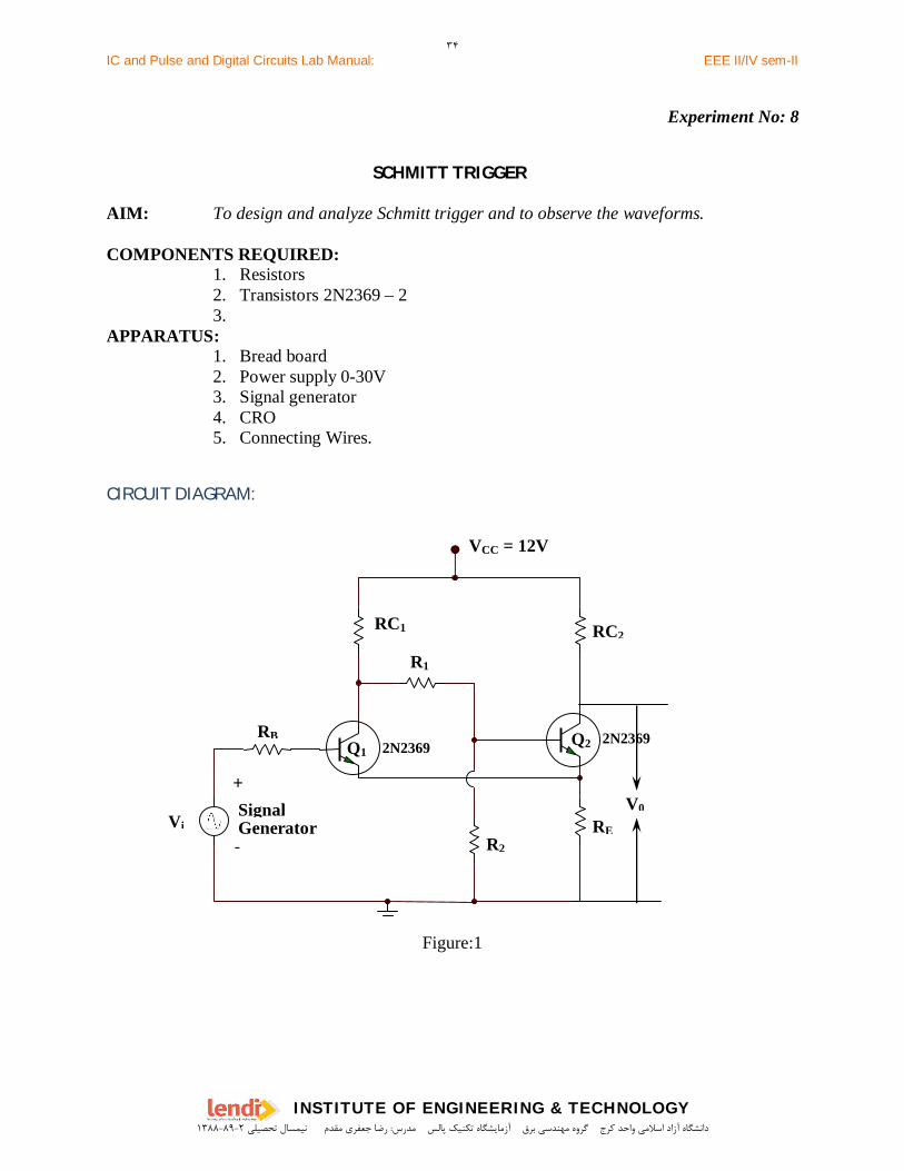
CIRCUIT DIAGRAM:
Figure:1
-
+
RB
RC1
R1
2N2369
RC2
R2
RESignalGenerator
VCC = 12V
2N2369Q1Q2
V0Vi
۳۴
دانشگاه آزاد اسالمي واحد كرج گروه مهندسي برق آزمايشگاه تكنيك پالس مدرس: رضا جعفري مقدم نيمسال تحصيلي 1۳۸۸-۸9-2
IC and Pulse and Digital Circuits Lab Manual: EEE II/IV sem-II
INSTITUTE OF ENGINEERING & TECHNOLOGY
THEORY:
The most important application of Schmitt Trigger circuit are amplitude comparator andsquaring circuit are amplitude comparator and squaring circuit. The circuit is used to obtain asquare waveform from any arbitrary input waveform. The loop gain is to be less than unity.
If Q2 is conducting there will be voltage drop across RZ which will elevate the emitter ofQ1. Consequently if V is small enough in voltage, Q1 will be cut-off with Q1 conducting, thecircuit amplifies and since the gain is positive, the output to rise, V2 continues to fall and Z2continues to rise. Therefore a value of V will be reached where Q2 is turned OFF. At the point theoutput no longer responds to the input.
Here the input signal is arbitrary except that it has large enough excursion to carry inputbeyond the limits of hysteresis range, VH = (V1 – V2).
The output is a square wave whose amplitude is independent of the amplitude of the inputwaveform.
DESIGN:IC2 = 5mA(Rc2 + RE) = VCC / IC2U.T.P = VE2 = 5VVE2 = (RE ×VCC) / (Rc2+RE)I2 = 0.1×IC2L.T.P = VE1 = 3VR2 = ER2i / I2 = VE1 / I2 = L.T.P / I2
Rc1 = (RE×VCC) / VE1 –REIB2 = IC2 / hfe(min)(VCC - VE2) / (R1+RL1))) = (VE2/R2)+IB2
RB = (hfe×RE) / 10Find R1, R2, RE, Rc1and Rc2 from the above equations
PROCEDURE:
1. Connect the circuit as shown in figure 1 with designed values.2. Apply VCC of 12V and an input frequency of 1KHz with an amplitude more than the
designed UTP.3. Now note down the output wave forms4. Observe that the output comes to ON state when input exceeds UTP and it comes to OFF
state when input comes below LTP5. Observe the waveforms at VC1, VC2, VB2 and VE and plot graphs.6. Keep the DC- AC control of the Oscilloscope in DC mode.
۳۵
دانشگاه آزاد اسالمي واحد كرج گروه مهندسي برق آزمايشگاه تكنيك پالس مدرس: رضا جعفري مقدم نيمسال تحصيلي 1۳۸۸-۸9-2
IC and Pulse and Digital Circuits Lab Manual: EEE II/IV sem-II
INSTITUTE OF ENGINEERING & TECHNOLOGY
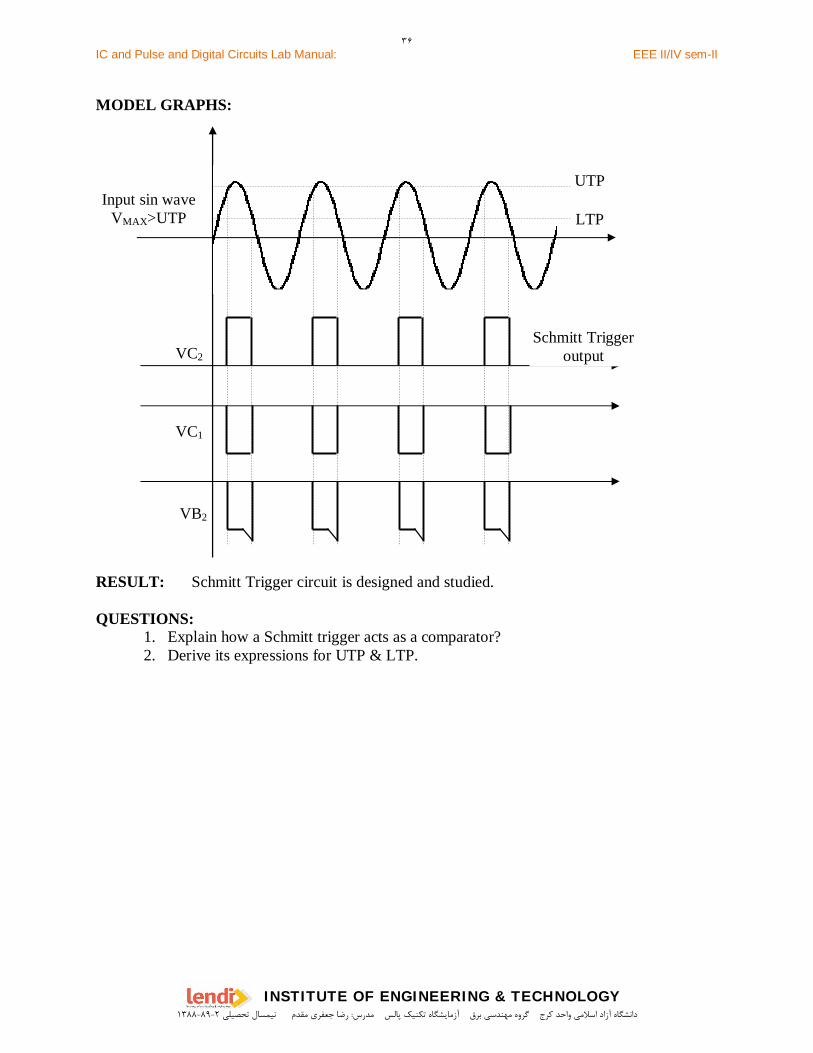
MODEL GRAPHS:
RESULT: Schmitt Trigger circuit is designed and studied.
QUESTIONS:1. Explain how a Schmitt trigger acts as a comparator?2. Derive its expressions for UTP & LTP.
VC2
VC1
VB2
Input sin waveVMAX>UTP
UTP
LTP
Schmitt Triggeroutput
۳۶
دانشگاه آزاد اسالمي واحد كرج گروه مهندسي برق آزمايشگاه تكنيك پالس مدرس: رضا جعفري مقدم نيمسال تحصيلي 1۳۸۸-۸9-2
IC and Pulse and Digital Circuits Lab Manual: EEE II/IV sem-II
INSTITUTE OF ENGINEERING & TECHNOLOGY
-
+
Ra=1K
RL
+Va
+Vb
+Vc
V2
Ia
Ib
Ic
IF
V1IB2≅0
IB1≅0
ROM = (Ra || Rb || Rc || RF)
+Vcc
-VEE
741
++−= c
c
Fb
b
Fa
a
F VRR
VRR
VRR
V0
Rb =1K
Rc=1K
Rf =1K
3
2 7
4
6
R1 RFV2
-+
RL
R
R
R
+Va
+Vb
+Vc
V1
Vcc
VEE
++
+=
3110
cbaF VVVRRV741
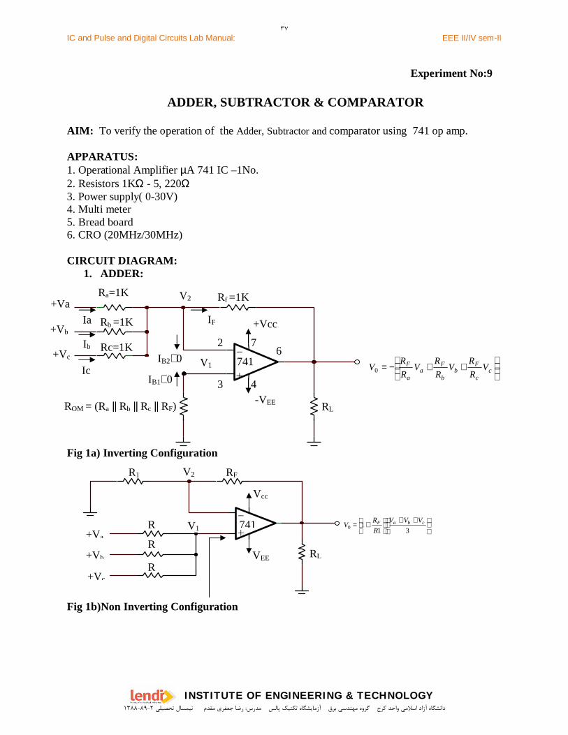
Experiment No:9
ADDER, SUBTRACTOR & COMPARATOR
AIM: To verify the operation of the Adder, Subtractor and comparator using 741 op amp.
APPARATUS:1. Operational Amplifier µA 741 IC –1No.2. Resistors 1KΩ - 5, 220Ω3. Power supply( 0-30V)4. Multi meter5. Bread board6. CRO (20MHz/30MHz)
CIRCUIT DIAGRAM:1. ADDER:
Fig 1a) Inverting Configuration
Fig 1b)Non Inverting Configuration
۳۷
دانشگاه آزاد اسالمي واحد كرج گروه مهندسي برق آزمايشگاه تكنيك پالس مدرس: رضا جعفري مقدم نيمسال تحصيلي 1۳۸۸-۸9-2
IC and Pulse and Digital Circuits Lab Manual: EEE II/IV sem-II
INSTITUTE OF ENGINEERING & TECHNOLOGY
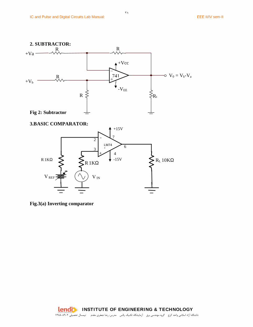
2. SUBTRACTOR:
Fig 2: Subtractor
3.BASIC COMPARATOR:
Fig.3(a) Inverting comparator
+Vcc-
+
-VEE
R
R
R
R RL
+Va
+Vb
V0 = Vb-Va741
+
-
+15V
-15V
LM741
2
3
7
4
6
RL 10KΩR 1KΩR 1KΩ
V REF V IN
۳۸
دانشگاه آزاد اسالمي واحد كرج گروه مهندسي برق آزمايشگاه تكنيك پالس مدرس: رضا جعفري مقدم نيمسال تحصيلي 1۳۸۸-۸9-2
IC and Pulse and Digital Circuits Lab Manual: EEE II/IV sem-II
INSTITUTE OF ENGINEERING & TECHNOLOGY
MODEL GRAPH:
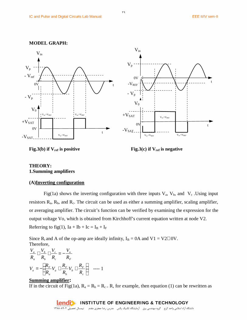
Fig.3(b) if Vref is positive Fig.3(c) if Vref is negative
THEORY:1.Summing amplifiers
(A)Inverting configuration
Fig(1a) shows the inverting configuration with three inputs Va, Vb, and Vc .Using input
resistors Ra, Rb, and Rc. The circuit can be used as either a summing amplifier, scaling amplifier,
or averaging amplifier. The circuit’s function can be verified by examining the expression for the
output voltage Vo, which is obtained from Kirchhoff’s current equation written at node V2.
Referring to fig(1), Ia + Ib + Ic = IB + IF
Since Ri and A of the op-amp are ideally infinity, IB = 0A and V1 = V2≅ 0V.Therefore,
F
o
c
c
b
b
a
a
RV
RV
RV
RV
−=++
++−=
c
Fb
b
Fa
a
Fo R
RVRRV
RRV ---- 1
Summing amplifier:If in the circuit of Fig(1a), Ra = Rb = Rc = R, for example, then equation (1) can be rewritten as
t
Vin
Vp
- Vp
- Vref
0V
0Vt
+VSAT
-VSAT
Vin >VREF Vin >VREF
Vin <VREF
V0
Vin
Vp
- Vp
0V-VREF
0V
t
t
+VSAT
-VSATVin <VREF Vin <VREF
Vin >VREF
V0
۳۹
دانشگاه آزاد اسالمي واحد كرج گروه مهندسي برق آزمايشگاه تكنيك پالس مدرس: رضا جعفري مقدم نيمسال تحصيلي 1۳۸۸-۸9-2
IC and Pulse and Digital Circuits Lab Manual: EEE II/IV sem-II
INSTITUTE OF ENGINEERING & TECHNOLOGY
( )cbaF
o VVVR
RV ++−=
This means that the output voltage is equal to the negative sum of all the inputs times the gain
of the circuit RF/R: Hence the circuit is called a summing amplifier.
(B)Non inverting Configuration:
If input voltages sources and resistors are connected to the non inverting terminal as
shown in fig (1b), the circuit can be used either as a summing or averaging amplifier through
selection of appropriate values of resistors, that is, R1 and RF.
Using the superposition theorem, the voltage V1 at the non inverting terminal is
cba VRR
RV
RR
RV
RR
RV
2
2
2
2
2
21
++
++
+=
33331cbacba VVVVVV
V++
=++= ---- 2
Hence the output voltage is Vo = 11
1 VRRF
+
=3
11
VcVVRR baF ++
+
Summing amplifier:
A close examination of equation (2) revels that if the gain (1+RF/R1) is equal to the
number of inputs, the output voltage becomes equal to the sum of all input voltages. That is, if
(1+RF/R1) = 3. (From equation (1)),
Vo = Va + Vb +VcHence the circuit is called a non inverting summing amplifier.2. Subtractor:
A basic differential amplifier can be used as a subtractor as shown in figure 2. In this
figure, input signals can be scaled to the desired values by selecting appropriate values for the
external resistors; when this is done, the circuit is referred to as scaling amplifier. However, in
figure 3 all external resistors are equal in value, so the gain of the amplifier is equal to 1. From
۴۰
دانشگاه آزاد اسالمي واحد كرج گروه مهندسي برق آزمايشگاه تكنيك پالس مدرس: رضا جعفري مقدم نيمسال تحصيلي 1۳۸۸-۸9-2
IC and Pulse and Digital Circuits Lab Manual: EEE II/IV sem-II
INSTITUTE OF ENGINEERING & TECHNOLOGY
the figure, the output voltage of the differential amplifier with a gain of 1 is
( )R
VVRV ba −
−=0
That is, ab VVV −=0
Thus the output voltage V0 is equal to the voltage applied to the non inverting terminal (Vb)
minus the voltage applied to the inverting terminal(Va);hence the circuit is called a subtractor.
3.Basic comparator: Figure (3) shows an op-amp used as a comparator. A fixed reference voltage Vref
of 1V is applied to the (-) input, and the other time-varying signal voltage Vin is applied to the (+)
input. Because of this arrangement, the circuit is called the noninverting comparator.
When Vin is less than Vref, the output voltage V0 is at –Vsat(≅-VEE) because the voltage at
the (-) input is higher than that at the (+) input. On the other hand, when Vin is greater than Vref,
the (+) input becomes positive with respect to the (-) input, and V0 goes to +Vsat (≅+Vcc). Thus
V0 changes from one saturation level to another whenever Vin ≅ Vref, as shown in figure 3(b).
In short, the comparator is a type of analog-to-digital converter. At any given time the V0
waveform shows whether Vin is greater or less than Vref. The comparator is sometimes also
called a voltage-level detector because, for a desired value of Vref, the voltage level of the input
Vin can be detected .
The resistance R in series with Vin is used to limit the current through D1 and D2.
To reduce offset problems, a resistance ROM≅R is connected between (-) input and Vref.
If the reference voltage Vref is negative with respect to ground, with sinusoidal signal
applied to the (+) input, the output waveforms will be as shown in Figure3(c).
When Vin>Vref, V0 is at +Vsat; on the other hand, when Vin<Vref, V0 is at –Vsat.
Obviously, the amplitude of Vin must be large enough to pass through Vref if the switching action
is to take place.
Figure (3) shows an inverting comparator in which the reference voltage Vref is applied to
the (+) input and Vin is applied to the (-) input. In this circuit, Vref is obtained by using a 10KΩ
potentiometer that forms a voltage divider with the dc supply voltage +Vcc and –VEE and the
wiper connected to the (+) input.
As the wiper is moved toward –VEE, Vref becomes more negative, while if it is moved
towards +Vcc, Vref becomes more positive. Thus a Vref of a desired amplitude and polarity can be
۴۱
دانشگاه آزاد اسالمي واحد كرج گروه مهندسي برق آزمايشگاه تكنيك پالس مدرس: رضا جعفري مقدم نيمسال تحصيلي 1۳۸۸-۸9-2

IC and Pulse and Digital Circuits Lab Manual: EEE II/IV sem-II
INSTITUTE OF ENGINEERING & TECHNOLOGY
obtained by simply adjusting the 10KΩ potentiometer. With the sinusoidal input waveform, the
output V0 has the waveform shown in Figure 3(a) or 3(b), depending on whether Vref is negative,
respectively.
PROCEDURE:Part 1: ADDER:1. Connect the circuit as shown in figure(1).
2. Apply different DC input voltages at Va, Vb, and Vc and
measure the output voltage Vo using a multi meter
It should be Vo = Va + Vb + Vc
Part 2: SUBTRACTOR:1. Connect the circuit as shown in figure(2).
2. Apply different DC input voltages at Va, and Vb and
measure the output voltage Vo using a multi meter .
It should be Vo = Vb – Va.
Part 3: COMPARATOR:1. Connect the circuit as shown in figure(3a).
2. Apply a reference voltage of (say 1V), to inverting terminal of op-amp.
3. Apply a sinusoidal wave with a peak voltage more than Vref to OP-AMPs
Non-inverting terminal.
4. Observe the output at pin number 6, which will be a square wave with peak to peak
voltage of (Vsat to –Vsat).
5. Observe that when Vref is less than Vin, then the output goes to +Vsat,
when Vref is greater than Vin then output goes to –Vsat.
6. Now set another reference voltage and repeat the steps 4 and 5.
7. Draw the observed waveforms on graph sheet and obtain the practical reference voltage.
Result:Hence the operation of Adder, Subtractor, and comparator (using 741 op amp) is verified.
Conclusions:It is observed that the out put Values are very much nearer to the given inputs. So we can
conclude that Adder, Subtractor, and comparator are functioning properly.
۴۲
دانشگاه آزاد اسالمي واحد كرج گروه مهندسي برق آزمايشگاه تكنيك پالس مدرس: رضا جعفري مقدم نيمسال تحصيلي 1۳۸۸-۸9-2
IC and Pulse and Digital Circuits Lab Manual: EEE II/IV sem-II
INSTITUTE OF ENGINEERING & TECHNOLOGY
Experiment No:10
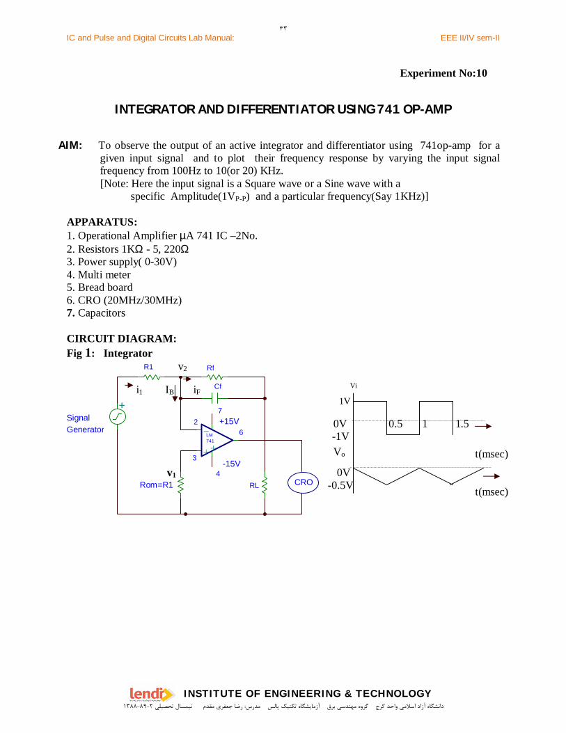
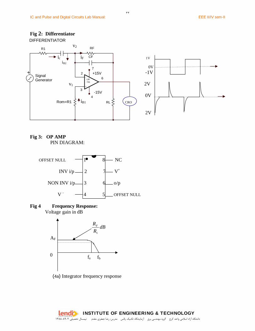
INTEGRATOR AND DIFFERENTIATOR USING 741 OP-AMP
AIM: To observe the output of an active integrator and differentiator using 741op-amp for agiven input signal and to plot their frequency response by varying the input signalfrequency from 100Hz to 10(or 20) KHz.
[Note: Here the input signal is a Square wave or a Sine wave with a specific Amplitude(1VP-P) and a particular frequency(Say 1KHz)]
APPARATUS:1. Operational Amplifier µA 741 IC –2No.2. Resistors 1KΩ - 5, 220Ω3. Power supply( 0-30V)4. Multi meter5. Bread board6. CRO (20MHz/30MHz)7. Capacitors
CIRCUIT DIAGRAM:Fig 1: Integrator
v2
i1 IB iF 1V
0V 0.5 1 1.5 -1V
v1 0V -0.5V
Vo
Vi
t(msec)
t(msec)
-
++
+
LM741
SignalGenerator
CRO
+15V
-15V
Rom=R1
2
3
6
R1 Rf
Cf
RL
7
4
۴۳
دانشگاه آزاد اسالمي واحد كرج گروه مهندسي برق آزمايشگاه تكنيك پالس مدرس: رضا جعفري مقدم نيمسال تحصيلي 1۳۸۸-۸9-2
IC and Pulse and Digital Circuits Lab Manual: EEE II/IV sem-II
INSTITUTE OF ENGINEERING & TECHNOLOGY
Fig 2: Differentiator
v2
ic iF 1V iB2
0V -1V
v1 2V
0ViB1 CRO
2V
Fig 3: OP AMP PIN DIAGRAM:
OFFSET NULL 1 8 NC
INV i/p 2 7 V+
NON INV i/p 3 6 o/p
V - 4 5 OFFSET NULL
Fig 4 Frequency Response:
-
+
+LM741
SignalGenerator
+15V
-15V
Rom=R1
2
3
6
R1 RF
CF
RL
DIFFERENTIATOR
7
4
(4a) Integrator frequency response
Voltage gain in dB
dBRRF
1
AF
fa fb0
۴۴
دانشگاه آزاد اسالمي واحد كرج گروه مهندسي برق آزمايشگاه تكنيك پالس مدرس: رضا جعفري مقدم نيمسال تحصيلي 1۳۸۸-۸9-2

IC and Pulse and Digital Circuits Lab Manual: EEE II/IV sem-II
INSTITUTE OF ENGINEERING & TECHNOLOGY
Gain dB
0
f fa fb 4b) Differentiator frequency response
THEORY:
A)INTEGRATOR:
A circuit in which “the output voltage waveform is the integral of the input voltage
waveform” is the integrator or the integration amplifier.
Such a circuit is obtained by using a basic inverting amplifier configuration, if the feed
back resistor RF is replaced by a capacitor CF.
Analysis of Integrator Circuit:
The expression for the output voltage v0 can be obtained by writing Kirchhoff’s currentequation at node v2:
i1 = IB + iFSince IB is negligibly small, i1 ≅ iFRecall that the relationship between current through and voltage across the capacitor is
iC = Cdt
dvc
Therefore, ( )011
21 vvdtdC
Rvv
F −
=
−
However, v1 = v2 ≅ 0 because A is very large. Therefore,
( )01
vdtdC
Rv
Fin −=
The output voltage can be obtained by integrating both sides with respect to time:
( )dtvdtdCdt
Rvt t
Fin
00 01
−=∫ ∫
= CF (-v0) + 00 =tv
۴۵
دانشگاه آزاد اسالمي واحد كرج گروه مهندسي برق آزمايشگاه تكنيك پالس مدرس: رضا جعفري مقدم نيمسال تحصيلي 1۳۸۸-۸9-2
IC and Pulse and Digital Circuits Lab Manual: EEE II/IV sem-II
INSTITUTE OF ENGINEERING & TECHNOLOGY
Therefore, v0 = ∫ +t
inF
CdtvCR 01
1 ------- 1
Where C is integration constant and is proportional to the value of the output voltage v0 at timet=0 seconds.
Equation 1 indicates that the output voltage is directly proportional to the negative integral of the
input voltage and inversely proportional to the time constant R1CF.
If the input to the integrator is a sine wave, the output will be a cosine wave, or if the
input is a square wave, the output will be a triangular wave.
In the circuit shown in figure the stability and the low frequency roll-off problems can be
corrected by the addition of a resistor R2 (RF). The term stability refers to a constant gain as
frequency of an input signal is varied over a certain range. Low frequency roll-off refers to the
rate of decrease in gain at lower frequencies. The input signal will be integrated properly if the
time period T of the signal is larger than or equal to RFCF.
• The frequency at which gain is 0 dB is given by fb =fCR12
1π
• The gain limiting frequency is given by fa =ff CRπ2
1
• The Values of fa and in turn R1Cf and RfCf Values should be selected such that fa<fb.
• Ex: If fa=0.1fb, then Rf=10R1.
• The input signal will be integrated properly, if the Time period of the signal T RfCf.
Applications:The integrator is most commonly used in analog computers and analog to digital
converters and signal wave shaping circuits.
B)DIFFERENTIATOR:
The circuit shown in figure performs the mathematical operation of differentiation that is
the output waveform is the derivative of the input waveforms.
The differentiator may be constructed from a basic inverting amplifier if an input resistor
R1 is replaced by a capacitor C1.
Analysis of Differentiator Circuit:
The expression for the output voltage v0 can be obtained by writing Kirchhoff’s current
equation at node v2 as follows:
۴۶
دانشگاه آزاد اسالمي واحد كرج گروه مهندسي برق آزمايشگاه تكنيك پالس مدرس: رضا جعفري مقدم نيمسال تحصيلي 1۳۸۸-۸9-2

IC and Pulse and Digital Circuits Lab Manual: EEE II/IV sem-II
INSTITUTE OF ENGINEERING & TECHNOLOGY
iC = IB + iF
Since IB ≅ 0,
iC = iF
( )F
in Rvvvv
dtdC 02
21−
=−
But v1 = v2 ≅ 0V, because A is very large. Therefore,
F
in
Rv
dtdvC 0
1 −=
Ordt
dvCRv in
F 10 −=
Thus the output v0 is equal to RFC1 times the negative instantaneous rate of change of the input
voltage vin with time.
Since the differentiator performs the reverse of the integrators function, a cosine wave input will
produce a sine wave output, or triangular wave input will produce a Square wave output.
The stability and the high frequency noise problems can be corrected by the addition of two
components R1 and CF.
• The frequency at which gain is 0 dB is given by fa =12
1CR fπ
• The gain limiting frequency is given by fb =112
1CRπ
where R1C1=RfCf
• The input signal will be differentiated properly, if the Time period of the signal T RfC1.
• From the frequency f to fb,the gain increases at 20dB/decade.However,after fb the gaindecreases at 20 dB/decade.
Applications:The differentiator is most commonly used in wave shaping circuits to detect high
frequency components in an input signal and also as a rate-of-change detector in FM modulator.
DESIGN :
Part 1:Design of IntegratorDesign an Integrator to Integrate an input signal, that varies infrequency from 1KHz to 10KHz.
[Note:Select T Rf Cf, where Rf Cf =afπ2
1 (T= input signal time period)]
1. Select fa = 1 KHz. Assume a value of Cf < 1 µf. (Let Cf = 0.1 µf)
۴۷
دانشگاه آزاد اسالمي واحد كرج گروه مهندسي برق آزمايشگاه تكنيك پالس مدرس: رضا جعفري مقدم نيمسال تحصيلي 1۳۸۸-۸9-2

IC and Pulse and Digital Circuits Lab Manual: EEE II/IV sem-II
INSTITUTE OF ENGINEERING & TECHNOLOGY
( fa is the gain limiting frequency)
2.Calculate the value of Rf using the formula Rf =faCfπ2
1
3. let fb=10fa ( fb is the frequency at which gain is 0 dB)
4.Calculate R1 using the formula R1=fbCfπ2
1 .
6.Choose Rom = R1. 6. Take load resistor RL = 10KΩ
Part 2: Design of Differentiator
Design a Differentiator to Differentiate an input signal, that varies infrequency from 1KHz to 20KHz.
1. Select fa = 1 KHz. Assume a value of C1 < 1 µf. (Let C1 = 0.1 µf) ( fa is the frequency at which gain is 0 dB)
2.Calculate the value of Rf using the formula Rf =12
1Cf aπ
(Result: Rf=1.59K ) 3. let fb= 20fa , fb is the gain limiting frequency
Calculate R1 using the formula R1=12
1Cfbπ
.
(Result: R1=79.5 ) 4. From R1C1 = RfCf calculate Cf (Result: C1=0.005µf)
5.Choose Rom = Rf.
6. Take load resistor RL = 10KΩ
PROCEDURE:
Part 1 1. By using the component values as per the above specified design,Connect the circuit
as shown in the figure.
2. Apply the 1VP-P, 1KHz Sinewave or Squarewave as input
3. Observe the output on CRO.
4. Draw the input and output Signals on the Graph paper.
Part 25. Vary the input signal (Preferably Sine wave) frequency from 100 Hz to10(or 20)KHz
and notedown the amplitude of the output signal (V0).
6. Claculate Gaini
o
VV
at each value of the input signal frequency.
۴۸
دانشگاه آزاد اسالمي واحد كرج گروه مهندسي برق آزمايشگاه تكنيك پالس مدرس: رضا جعفري مقدم نيمسال تحصيلي 1۳۸۸-۸9-2

IC and Pulse and Digital Circuits Lab Manual: EEE II/IV sem-II
INSTITUTE OF ENGINEERING & TECHNOLOGY
Also Calculate dB Value of Gain 20logi
o
VV
.
7. Plot the graph between frequency (on X-Axis) and
dB Value of Gain 20logi
o
VV
(on Y-Axis)
8. Identify the Practical Values of faand fb from the Graphs.
(Note: The Practical Values of faand fb observed from the Graphs must equal to the
Theoritical values)
Result: Hence the output of an active integrator and differentiator using op-amp 741 for agiven input signal is observed and plotted their frequency response by varying theinput signal frequency from 100Hz to 10(or 20) KHz.
Conclusions: The Practical Values of faand fb observed from the Graphs are equal to the
Theoritical values. From this we can conclude that the Integrator and
Differentiator using 741 OP-AMP are satisfying their function properly.
۴۹
دانشگاه آزاد اسالمي واحد كرج گروه مهندسي برق آزمايشگاه تكنيك پالس مدرس: رضا جعفري مقدم نيمسال تحصيلي 1۳۸۸-۸9-2
IC and Pulse and Digital Circuits Lab Manual: EEE II/IV sem-II
INSTITUTE OF ENGINEERING & TECHNOLOGY
Frequency0.707AF
Experiment No.11
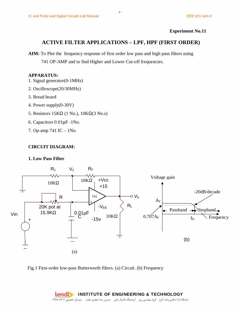
ACTIVE FILTER APPLICATIONS – LPF, HPF (FIRST ORDER)
AIM: To Plot the frequency response of first order low pass and high pass filters using
741 OP-AMP and to find Higher and Lower Cut-off frequencies.
APPARATUS:1. Signal generator(0-1MHz)
2. Oscilloscope(20/30MHz)
3. Bread board
4. Power supply(0-30V)
5. Resistors 15KΩ (1 No.), 10KΩ(3 No.s)
6. Capacitors 0.01µF -1No.
7. Op-amp 741 IC – 1No.
CIRCUIT DIAGRAM:
1. Low Pass Filter
(a)
V0
-
+
R1 RF
+Vcc
-VEE RL
R
Vin C
741
+15
-15v
10KΩ 10KΩ
10KΩ
V2
20K pot at 15.9KΩ 0.01µF
+
Voltage gain
Passband Stopband
-20dB/decade
AF
fH
(b)
Fig.1 First-order low-pass Butterworth filters. (a) Circuit. (b) Frequency
۵۰
دانشگاه آزاد اسالمي واحد كرج گروه مهندسي برق آزمايشگاه تكنيك پالس مدرس: رضا جعفري مقدم نيمسال تحصيلي 1۳۸۸-۸9-2
IC and Pulse and Digital Circuits Lab Manual: EEE II/IV sem-II
INSTITUTE OF ENGINEERING & TECHNOLOGY
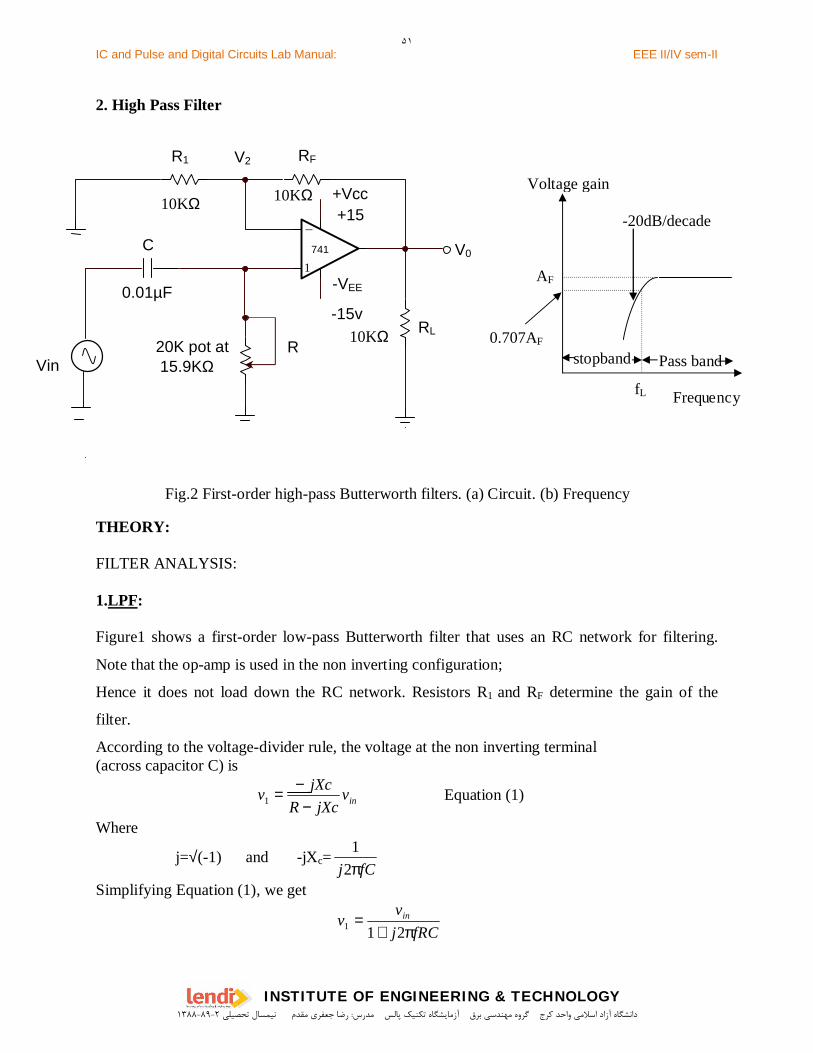
2. High Pass Filter
THEORY:
FILTER ANALYSIS:
1.LPF:
Figure1 shows a first-order low-pass Butterworth filter that uses an RC network for filtering.
Note that the op-amp is used in the non inverting configuration;
Hence it does not load down the RC network. Resistors R1 and RF determine the gain of the
filter.
According to the voltage-divider rule, the voltage at the non inverting terminal(across capacitor C) is
invjXcR
jXcv−
−=1 Equation (1)
Where
j=√(-1) and -jXc= fCj π21
Simplifying Equation (1), we get
fRCjv
v in
π211 +=
Vin
Fig.2 First-order high-pass Butterworth filters. (a) Circuit. (b) Frequencyresponse
-
1
R1 RF
+Vcc
-VEE
RL
R
C 741
+15
-15v
10KΩ 10KΩ
10KΩ
V2
20K pot at 15.9KΩ
0.01µF
V0
Voltage gain
Frequency
AF
0.707AF
stopbanddd
Pass band
-20dB/decade
fL
۵۱
دانشگاه آزاد اسالمي واحد كرج گروه مهندسي برق آزمايشگاه تكنيك پالس مدرس: رضا جعفري مقدم نيمسال تحصيلي 1۳۸۸-۸9-2

IC and Pulse and Digital Circuits Lab Manual: EEE II/IV sem-II
INSTITUTE OF ENGINEERING & TECHNOLOGY
And the output voltage
11
0 )1( vRRv F+=
That is, fRCjv
RRv inF
π21)1(
10 +
+=
)/(10
H
F
in ffjA
vv
+= - Equation (2)
Whereinv
v0 = gain of the filter as a function of frequency
)1(1R
RA F
F += = pass band gain of the filter
f = frequency of the input signal
RCf H π2
1= = high cutoff frequency of the filter
The gain magnitude and phase angle equations of the low-pass filter can be obtained byconverting Equation-(2) into its equivalent polar form, as follows:
( )2)/(10
H
F
ffA
VinV
+√= - Equation-(3)
Φ = -tan-1
Hff
Where Φ is the phase angle in degrees.
The operation of the low-pass filter can be verified from the gain magnitude equation (3):
1. At very low frequencies, that is, f<fH,
VinV 0 ≅ AF
2. At f=fH VinV 0 = F
F AA
707.02
=√
3. At f>fH,VinV 0
< AF
Thus the low-pass filter has a constant gain AF from 0 Hz to the high cutoff frequency fH.
At fH the gain is 0.707 AF, and after fH it decreases at a constant rate with an increase in
frequency see Fig1b. That is, when the frequency is increased to tenfold (one decade), the
voltage gain is divided by 10.
۵۲
دانشگاه آزاد اسالمي واحد كرج گروه مهندسي برق آزمايشگاه تكنيك پالس مدرس: رضا جعفري مقدم نيمسال تحصيلي 1۳۸۸-۸9-2
IC and Pulse and Digital Circuits Lab Manual: EEE II/IV sem-II
INSTITUTE OF ENGINEERING & TECHNOLOGY
In other words, the gain decreases 20db (=20 log 10) each time the frequency is increased by 10.
Hence the rate at which the gain rolls off after fH is 20 db/decode or 6 db/octave, where octave
signifies a twofold increase in frequency.
The frequency f= fH is called the higher cutoff frequency because the gain of the filter at this
frequency is down by 3 db (=20 log 0.707) from 0 Hz. Other equivalent terms for cutoff
frequency are -3db frequency, break frequency, or corner frequency.
HPF:
High-pass filters are often formed simply by interchanging frequency-determining
resistors and capacitors in low-pass filters. That is, a first-order high-pass filter is formed from a
first-order low-pass type by interchanging components R and C. Similarly, a second-order high-
pass filter is obtained from a second-order low-pass filter if R and C are interchanged, and so on.
Figure2 shows a first-order high-pass Butterworth filter with a low cutoff frequency of fL. This is
the frequency at which the magnitude of the gain is 0.707 times its pass band value. Obviously,
all frequencies higher than fL are pass band frequencies, with the highest frequency determined
by the closed-loop bandwidth of the op-amp.
Note that the high-pass filter of figure2(a) and the low-pass filter of figure(1a) are the
same circuits, except that the frequency-determining components (R and C) are interchanged.
For the first-order high-pass filter of Figure, the output voltage is
inF V
fRCjfRCj
RRV
ππ21
2)1(1
0 ++=
or( )
( )
+=
L
LF ffj
ffjAVinV
/1/0
Where )1(1R
RA F
F += = pass band gain of the filter
f= frequency of the input signal (Hz) fL= RCπ2
1 = low cutoff frequency (Hz)Hence the magnitude of the voltage gain is
۵۳
دانشگاه آزاد اسالمي واحد كرج گروه مهندسي برق آزمايشگاه تكنيك پالس مدرس: رضا جعفري مقدم نيمسال تحصيلي 1۳۸۸-۸9-2

IC and Pulse and Digital Circuits Lab Manual: EEE II/IV sem-II
INSTITUTE OF ENGINEERING & TECHNOLOGY
( )( )( )2
0
/1/
L
LF
ffffA
VinV
+√=
Since high-pass filters are formed from low-pass filters simply by interchanging R’s and C’s, the
design procedure of the low-pass filter is also applicable to the high-pass filters
FILTER DESIGN:
A)LPF Design:Design a LPF having Cutoff frequency of 1KHz with a Passband gain of 2.
A low-pass filter can be designed by implementing the following steps:
1. Choose a value of high cutoff frequency fH (let us take 1KHz)
2. Select a value of C less than or equal to 1µf. ( let us take C=0.01µf .)
3. Calculate the value of R using the formulaCf
RHπ2
1= (It will become 15.9 K )
4. Finally, select values of R1 and RF dependent on the desired pass band gain AF using
)1(1R
RA F
F += [Since AF=2,then R1 = RF. Let R1 = RF =10K ]
5.Let RL=10K .
A)HPF Design:
Design a HPF having Cutoff frequency of 1KHz with a Passband gain of 2.
A High-pass filter can be designed by implementing the following steps:
1. Choose a value of low cutoff frequency fL (let us take 1KHz)
2. Select a value of C less than or equal to 1µf. ( let us take C=0.01µf .)
3. Calculate the value of R using the formulaCf
RLπ2
1= (It will become 15.9 K )
4. Finally, select values of R1 and RF dependent on the desired pass band gain AF using
)1(1R
RA F
F += [Since AF=2,then R1 = RF. Let R1 = RF =10K ]
5.Let RL=10K .
۵۴
دانشگاه آزاد اسالمي واحد كرج گروه مهندسي برق آزمايشگاه تكنيك پالس مدرس: رضا جعفري مقدم نيمسال تحصيلي 1۳۸۸-۸9-2

IC and Pulse and Digital Circuits Lab Manual: EEE II/IV sem-II
INSTITUTE OF ENGINEERING & TECHNOLOGY
Note:
It is better to take a Capacitor of a standard(fixed)value,not a Variable Capacitor.
If we take Variable Capacitor Value, some times, the Filter may give bad Response(output).
So in the above Design Procedure,we have Chosen a fixed value for the Capacitor,
not a Variable Capacitor,and then Calculated the value of Resistor for a desired frequency.
PROCEDURE:
LOW PASS FILTER& HIGH PASS FILTER FREQUENCY RESPONSE
1.Connect the circuit as shown in figure
2.Take a signal generator and observe its output (sinusoidal signal) on CRO.
Adjust the Amplitude of the sinusoidal signal(Vi) as 1Vp-p.Keep its frequency as 100Hz.
2.Connect the signal generator to the input of the LPF.
Using CRO observe the input and output waveforms simultaneously.
3 Vary the frequency of input signal from 100Hz to 100KHz
4. Measure the output voltage Amplitude(Vo) for every input frequency using oscilloscope.
5.Claculatethe Gain of the Filteri
o
VV
. Also Calculate its dB Value.
5. Draw the graph between frequency (Hz) on X-Axis and the Gain on Y –axis
on semi -log sheet.
6.Calculate the cut off frequency from the graph.This is the Practical value of Cut off frequency.
[from the graph find the value of Cut off frequency,at which the Gain is 0.707 times that of Pass band gain(AF)].
7.Compare the Practical values with Theoritical values.
۵۵
دانشگاه آزاد اسالمي واحد كرج گروه مهندسي برق آزمايشگاه تكنيك پالس مدرس: رضا جعفري مقدم نيمسال تحصيلي 1۳۸۸-۸9-2

IC and Pulse and Digital Circuits Lab Manual: EEE II/IV sem-II
INSTITUTE OF ENGINEERING & TECHNOLOGY
OBSERVATIONS:
Input Signal Amplitude(Vin) = 1Vp-p
Frequency(Hz)
Outputvoltage(Vo)
Gain = Vo/Vin Gain(in dB) =20log (Vo/Vin)
100Hz200Hz400Hz600Hz800Hz900Hz950Hz980Hz1KHz1.1KHz1.2KHz1.4KHz2KHz....100KHz
Result:Hence the frequency response of first order low pass and high pass filters using
741 OP-AMP were plotted,and Claculated the Higher and Lower Cut-off frequencies,
From Graphs.
Conclusions:The Practical values are same as the theoritical values in both the cases(ie.,LPF&HPF)
In the First case,for the frequencies below 1KHz the Filter’s Gain is Constant and after 1KHz
there is a decrease in the Gain. So it is Called as LowPass Filter.
In the Second case,for the frequencies above 1KHz the Filter’s Gain is Constant and below
1KHz there is a decrease in the Gain. So it is Called as High Pass Filter.
۵۶
دانشگاه آزاد اسالمي واحد كرج گروه مهندسي برق آزمايشگاه تكنيك پالس مدرس: رضا جعفري مقدم نيمسال تحصيلي 1۳۸۸-۸9-2
IC and Pulse and Digital Circuits Lab Manual: EEE II/IV sem-II
INSTITUTE OF ENGINEERING & TECHNOLOGY
Experiment-12
FUNCTION GENERATOR USING 741 OP-AMP
AIM: To generate triangular waveform using 741 Op-Amp function generator.
APPARATUS: Op-amp 741-2No, Capacitor – 0.1µf – 1No, Zener diode – 5Z1 – 2No, Resistors –10K-2, 150K-1, 15K-1, 1M-1, 8.2KΩ-1
CIRCUIT DIAGRAM:
OUTPUT WAVEFORMS
37
2
6 741 741
+15V
-15V
+15V
-15V
4
6
7
273
R1=10K
C= 0.05µF
Ri= 14K
R2=28K
VAVB
4
t(ms)
+Vsat
15
VUT 5
0
-5
- 10
- 15
-Vsat
VLT
1 2 3
VB
۵۷
دانشگاه آزاد اسالمي واحد كرج گروه مهندسي برق آزمايشگاه تكنيك پالس مدرس: رضا جعفري مقدم نيمسال تحصيلي 1۳۸۸-۸9-2
IC and Pulse and Digital Circuits Lab Manual: EEE II/IV sem-II
INSTITUTE OF ENGINEERING & TECHNOLOGY
Pin out diagram of LM 741 IC
OFFSET NULL 1 8 NC
INV I/P 2 7 V +
NON INV I/P 3 6 O/P
V - 4 5 OFFSET NULL
THEORY:
A basic bipolar triangle wave generator circuit is presented in fig 1 . The triangle wave
VA , is available at the output of the 741 integrator circuit . The square wave signal VB, is
available at the output of the 741 comparator . Assume that VB is high at +Vsat. This forces a
constant current (Vsat/Ri) through C (left to right) to drive VA negative from VUT to VLT. When
VA reaches VLT, Pin 3 of the comparator goes negative and VB snaps to –Vsat. And t =1msec.
When VB is at -Vsat , it forces a constant current( right to left) through C to drive VA
positive from VLT toward VUT ( the time interval 1 to 2 msec) . When VA reaches VUT at t=
2msec , pin 3 of the comparator goes positive and VB snaps to +Vsat. This initiates the next cycle
of oscillation .
Frequency of OperationThe peak values of the triangular wave are established by the ratio of resistor R2 to R and
the saturation voltages .
They are given by2
1
RRVV sat
UT−
=
2
1
RRVV sat
LT =
If the saturation voltages are reasonable equal , the frequency of oscillation (f) is given by
CRRRfi 1
2
4=
۵۸
دانشگاه آزاد اسالمي واحد كرج گروه مهندسي برق آزمايشگاه تكنيك پالس مدرس: رضا جعفري مقدم نيمسال تحصيلي 1۳۸۸-۸9-2
IC and Pulse and Digital Circuits Lab Manual: EEE II/IV sem-II
INSTITUTE OF ENGINEERING & TECHNOLOGY
PROCEDURE:
1. Connect the circuit as shown in the figure.
2. Observe the output waveforms on CRO and note down necessary readings and
waveforms.
3. Calculate the time period and amplitude of the waveform theoretically.
4. Compare the theoretical values with the experimental results.
RESULT:
Hence triangular waveform is generated using 741 Op-Amp function generator .
CONCLUSIONS:
It can be concluded that the 741 integrator has produced a triangle wave (VA) and the 741comparator has produced a square wave( VB )with amplitude levels –Vsat to +Vsat.The outputof the 741 comparator was given to the integrators input . That means integration of square wavegives the triangle wave.
۵۹
دانشگاه آزاد اسالمي واحد كرج گروه مهندسي برق آزمايشگاه تكنيك پالس مدرس: رضا جعفري مقدم نيمسال تحصيلي 1۳۸۸-۸9-2
IC and Pulse and Digital Circuits Lab Manual: EEE II/IV sem-II
INSTITUTE OF ENGINEERING & TECHNOLOGY
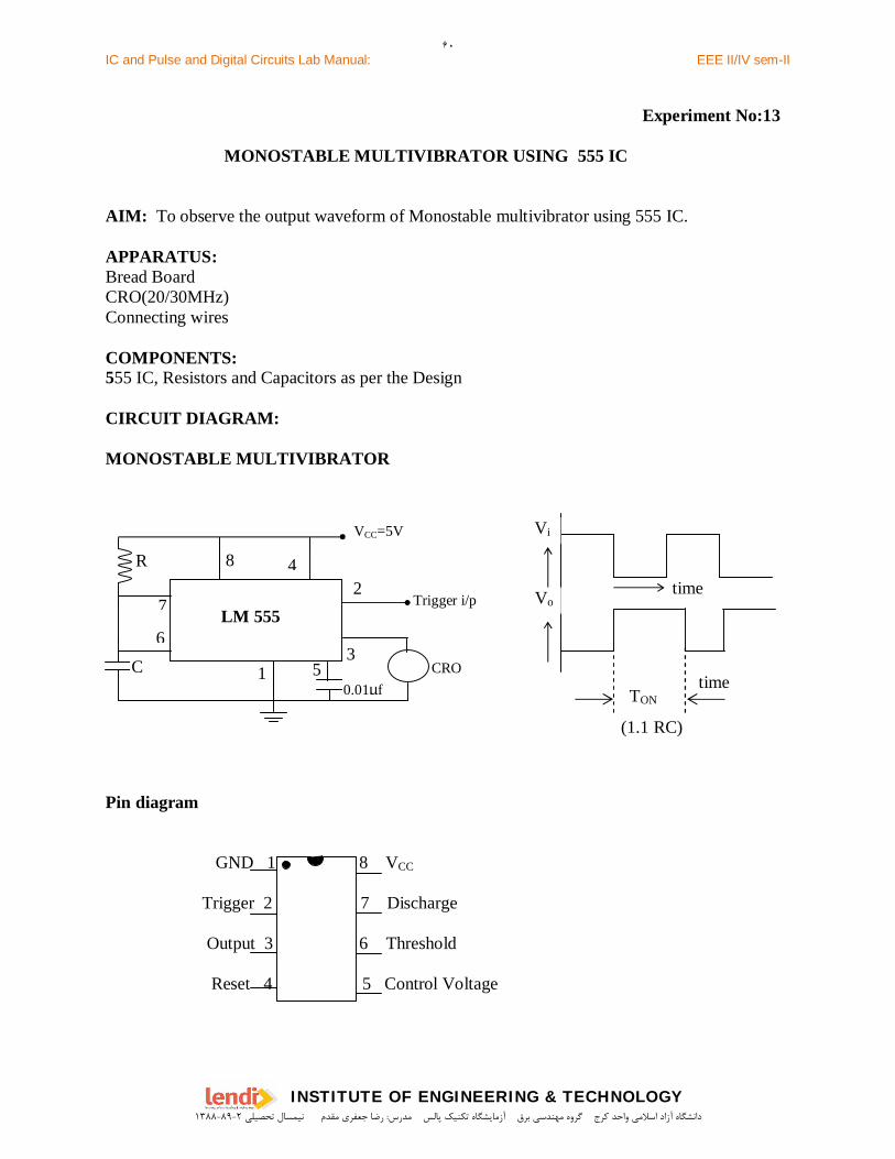
Experiment No:13
MONOSTABLE MULTIVIBRATOR USING 555 IC
AIM: To observe the output waveform of Monostable multivibrator using 555 IC.
APPARATUS:Bread BoardCRO(20/30MHz)Connecting wires
COMPONENTS:555 IC, Resistors and Capacitors as per the Design
CIRCUIT DIAGRAM:
MONOSTABLE MULTIVIBRATOR
Pin diagram
GND 1 8 VCC
Trigger 2 7 Discharge
Output 3 6 Threshold
Reset 4 5 Control Voltage
LM 5
55
7
6
4
1
5553
27
6
4
1 5
LM 555
0.01µf
R
C
8
CRO
VCC=5V
Trigger i/p
Vi
Vo
TONtime
time
(1.1 RC)
۶۰
دانشگاه آزاد اسالمي واحد كرج گروه مهندسي برق آزمايشگاه تكنيك پالس مدرس: رضا جعفري مقدم نيمسال تحصيلي 1۳۸۸-۸9-2
IC and Pulse and Digital Circuits Lab Manual: EEE II/IV sem-II
INSTITUTE OF ENGINEERING & TECHNOLOGY
THEORY:
THE 555 AS AN MONOSTABLE MULTIVIBRATOR:
A Monostable multivibrator is also called as a one-shot multivibrator is a pulse-generating circuit in which the duration of the pulse is determined by the RC network connectedexternally to the 555 timer. In a stable state the output of the circuit is zero or at logic-low level.
When an external trigger pulse is applied, the output is forced to go high (≅Vcc). Thetime the output remains high is determined by the external RC network connected to the timer.At the end of the timing interval, the output automatically reverts back to its logic low stablestate. The output stays low until the trigger pulse is again applied. Then the cycle repeats. Themonostable multivibrator has only the stable state.
The applications for the monostable multi vibrator are frequency divider and pulsestretcher
DESIGN:
Dersign a MMV using 555IC to produce an Output Pulse width of 10msec.
1.Let R=10K
2.Claculate the value of C using the formulaR
TC p
1.1=
PROCEDURE: 1.Connect the circuit as shown in the figure, by using the component as per design.
2. Apply the Trigger pulse at Pin no 2. Observe the output waveform at pin no 3.
3.Calculate the time during which the output remains high(tp or tonor Tp)
4.Compare it with the theoritical value.
RESULT:The output of Monostable multivibrator using 555IC is observed. It is also observed that
practical value of the time during which the output remains high is same as theoritical value.
CONCLUSIONS:
It can be concluded that,if the MMV is once triggered,its output will remain in the high state
until the set time elapses.The output will not change its state even if an input trigger is applied
again during this time interval Tp.
۶۱
دانشگاه آزاد اسالمي واحد كرج گروه مهندسي برق آزمايشگاه تكنيك پالس مدرس: رضا جعفري مقدم نيمسال تحصيلي 1۳۸۸-۸9-2
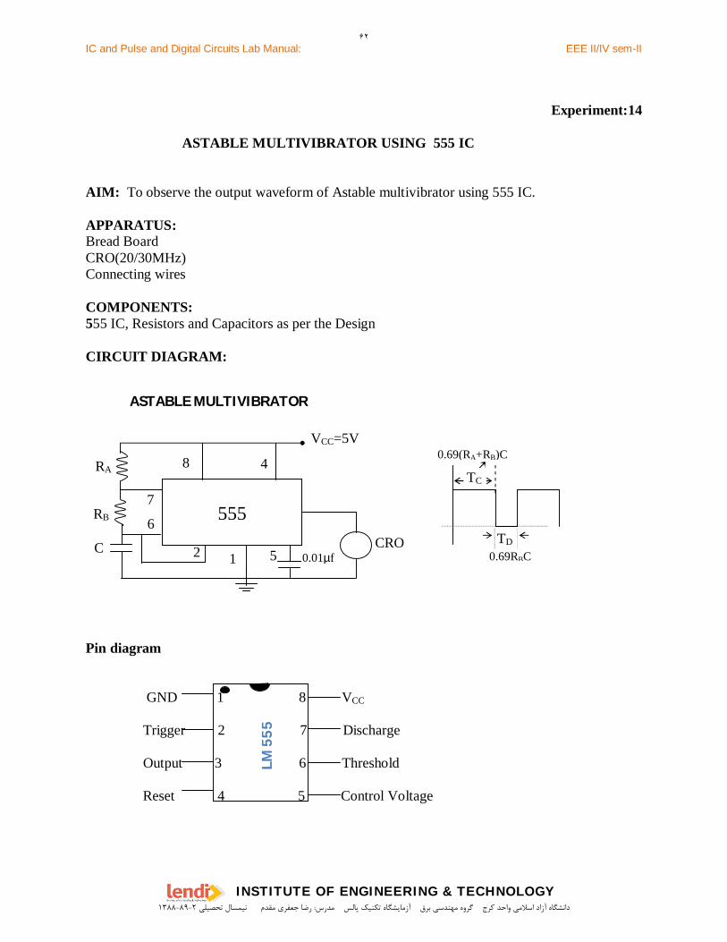
IC and Pulse and Digital Circuits Lab Manual: EEE II/IV sem-II
INSTITUTE OF ENGINEERING & TECHNOLOGY
Experiment:14
ASTABLE MULTIVIBRATOR USING 555 IC
AIM: To observe the output waveform of Astable multivibrator using 555 IC.
APPARATUS:Bread BoardCRO(20/30MHz)Connecting wires
COMPONENTS:555 IC, Resistors and Capacitors as per the Design
CIRCUIT DIAGRAM:
ASTABLE MULTIVIBRATOR
3RB 3
Pin diagram
GND 1 8 VCC
Trigger 2 7 Discharge
Output 3 6 Threshold
Reset 4 5 Control Voltage
LM 5
55
0.69(RA+RB)C
0.69RBC
TC
TD
57
6
8
2 1 5
555
RA
RB
0.01µfCRO
VCC=5V
4
C
۶۲
دانشگاه آزاد اسالمي واحد كرج گروه مهندسي برق آزمايشگاه تكنيك پالس مدرس: رضا جعفري مقدم نيمسال تحصيلي 1۳۸۸-۸9-2

IC and Pulse and Digital Circuits Lab Manual: EEE II/IV sem-II
INSTITUTE OF ENGINEERING & TECHNOLOGY
THEORY:
An Astable multivibrator, often called as free-running multivibrator, is a rectangular-wave-
generating circuit. This circuit does not require an external trigger to change the stable of the
output, hence the name free-running. However the time during which the output is either high or
low is determined by two resistors and a capacitor. Which are externally connected to the 555
timer.
The applications for astable multivibrator are (1) Square-wave oscillator (2) Free-running ramp
generator.
DESIGN:Design an Astable Multivibrator using 555IC to produce an output pulse with a
positive pulse width(Tc)=0.421msec and a a negative pulse width (Td)=0.269msec.
Let Tc = 0.69 (RA+RB) C ---1, where Tc is the time during which the output is high.
Let Td = 0.69 RBC------------2, where Td is the time during which the output is low
Calculate T = Tc+Td
1.Select C = 0.1 µF.
2.calculate RB using Equation 2
3.using the results in steps1,2,calculate RA using Equation 1
PROCEDURE: 1.Connect the circuit as shown in the figure.
2.Select the component values as per design.
3. Observe the output waveform at pin no 3.
4.Calculate the time during which the output is high and output is low.
Compare it with theoritical values.
5.Calculate the % duty cycle using the formula (Tc / T)*100. Compare it with theoritical
value.
۶۳
دانشگاه آزاد اسالمي واحد كرج گروه مهندسي برق آزمايشگاه تكنيك پالس مدرس: رضا جعفري مقدم نيمسال تحصيلي 1۳۸۸-۸9-2

IC and Pulse and Digital Circuits Lab Manual: EEE II/IV sem-II
INSTITUTE OF ENGINEERING & TECHNOLOGY
RESULT:
The output of Astable Multivibrator using 555IC is observed.
It is also observed that practical value of the time during which the output remains high and
output is low is same as theoritical value.
CONCLUSIONS:
It can be concluded that by changing the values of the Components (i.e., RA, RB and C),the
Pulse widths will be changed.
۶۴
دانشگاه آزاد اسالمي واحد كرج گروه مهندسي برق آزمايشگاه تكنيك پالس مدرس: رضا جعفري مقدم نيمسال تحصيلي 1۳۸۸-۸9-2
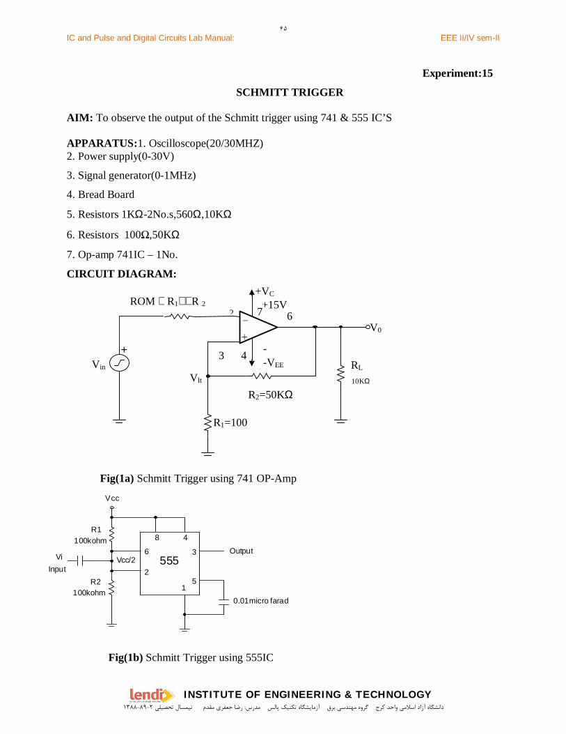
IC and Pulse and Digital Circuits Lab Manual: EEE II/IV sem-II
INSTITUTE OF ENGINEERING & TECHNOLOGY
V cc
R1100kohm
R2 100kohm
Vcc/2 555Output
0.01micro farad
InputVi
6
2
8 4
3
51
Experiment:15
SCHMITT TRIGGER
AIM: To observe the output of the Schmitt trigger using 741 & 555 IC’S
APPARATUS:1. Oscilloscope(20/30MHZ)2. Power supply(0-30V)
3. Signal generator(0-1MHz)
4. Bread Board
5. Resistors 1KΩ-2No.s,560Ω,10KΩ
6. Resistors 100 ,50KΩ
7. Op-amp 741IC – 1No.
CIRCUIT DIAGRAM:
Fig(1a) Schmitt Trigger using 741 OP-Amp
Fig(1b) Schmitt Trigger using 555IC
-
++
ROM ≅ R1R 2+VC
-VEE
+15V
-15V RL
10KΩ
R2=50KΩVlt
Vin
V0
2
3 4
7 6
R1=100Ω
۶۵
دانشگاه آزاد اسالمي واحد كرج گروه مهندسي برق آزمايشگاه تكنيك پالس مدرس: رضا جعفري مقدم نيمسال تحصيلي 1۳۸۸-۸9-2
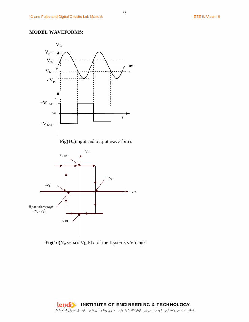
IC and Pulse and Digital Circuits Lab Manual: EEE II/IV sem-II
INSTITUTE OF ENGINEERING & TECHNOLOGY
MODEL WAVEFORMS:
Vlt
V0
Fig(1C)Input and output wave forms
Fig(1d)Vo versus Vin Plot of the Hysterisis Voltage
t
Vin
Vp
- Vp
- Vut
0V
0Vt
+VSAT
-VSAT
+Vsat
+VIt
+Vut
-Vsat
Vo
Vin
Hysteresis voltage (Vut-Vit)
۶۶
دانشگاه آزاد اسالمي واحد كرج گروه مهندسي برق آزمايشگاه تكنيك پالس مدرس: رضا جعفري مقدم نيمسال تحصيلي 1۳۸۸-۸9-2
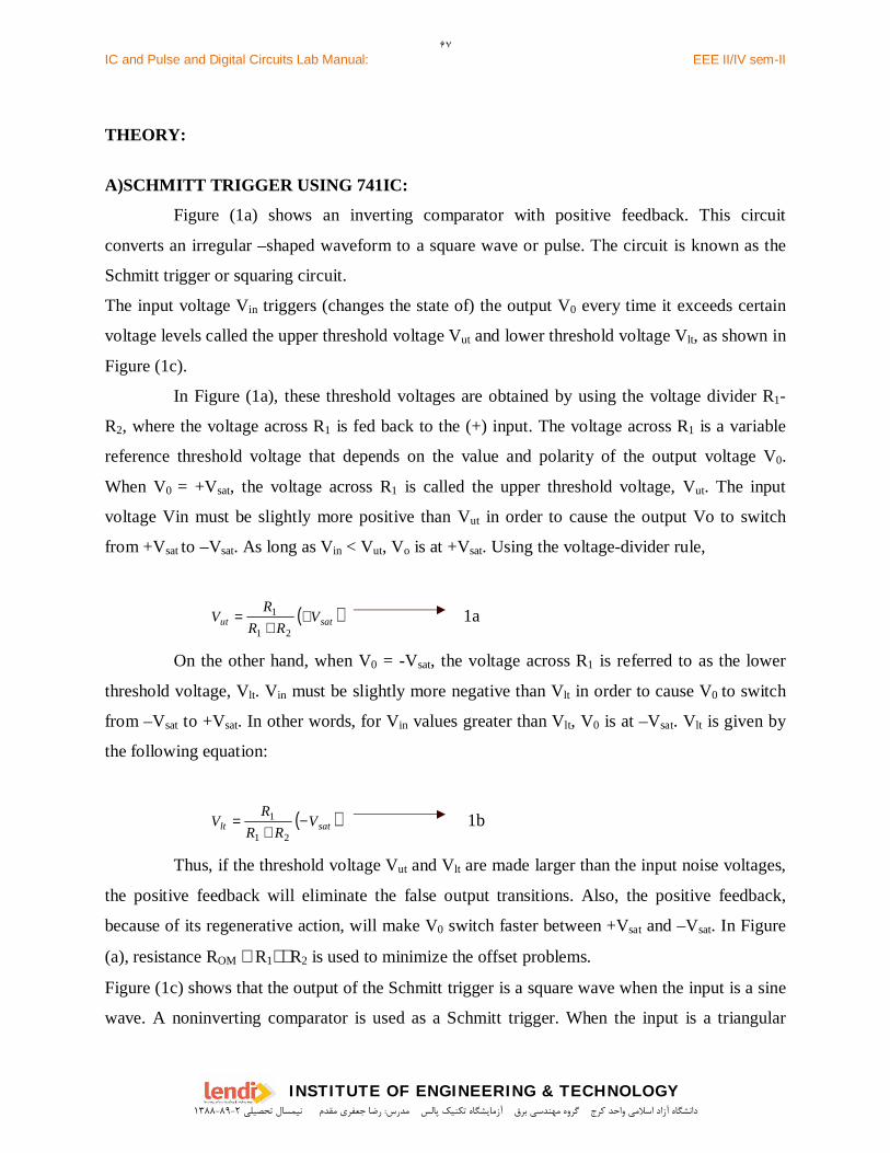
IC and Pulse and Digital Circuits Lab Manual: EEE II/IV sem-II
INSTITUTE OF ENGINEERING & TECHNOLOGY
THEORY:
A)SCHMITT TRIGGER USING 741IC:
Figure (1a) shows an inverting comparator with positive feedback. This circuit
converts an irregular –shaped waveform to a square wave or pulse. The circuit is known as the
Schmitt trigger or squaring circuit.
The input voltage Vin triggers (changes the state of) the output V0 every time it exceeds certain
voltage levels called the upper threshold voltage Vut and lower threshold voltage Vlt, as shown in
Figure (1c).
In Figure (1a), these threshold voltages are obtained by using the voltage divider R1-
R2, where the voltage across R1 is fed back to the (+) input. The voltage across R1 is a variable
reference threshold voltage that depends on the value and polarity of the output voltage V0.
When V0 = +Vsat, the voltage across R1 is called the upper threshold voltage, Vut. The input
voltage Vin must be slightly more positive than Vut in order to cause the output Vo to switch
from +Vsat to –Vsat. As long as Vin < Vut, Vo is at +Vsat. Using the voltage-divider rule,
( )satut VRR
RV +
+=
21
1 1a
On the other hand, when V0 = -Vsat, the voltage across R1 is referred to as the lower
threshold voltage, Vlt. Vin must be slightly more negative than Vlt in order to cause V0 to switch
from –Vsat to +Vsat. In other words, for Vin values greater than Vlt, V0 is at –Vsat. Vlt is given by
the following equation:
( )satlt VRR
RV −
+=
21
1 1b
Thus, if the threshold voltage Vut and Vlt are made larger than the input noise voltages,
the positive feedback will eliminate the false output transitions. Also, the positive feedback,
because of its regenerative action, will make V0 switch faster between +Vsat and –Vsat. In Figure
(a), resistance ROM ≅ R1R2 is used to minimize the offset problems.
Figure (1c) shows that the output of the Schmitt trigger is a square wave when the input is a sine
wave. A noninverting comparator is used as a Schmitt trigger. When the input is a triangular
۶۷
دانشگاه آزاد اسالمي واحد كرج گروه مهندسي برق آزمايشگاه تكنيك پالس مدرس: رضا جعفري مقدم نيمسال تحصيلي 1۳۸۸-۸9-2
IC and Pulse and Digital Circuits Lab Manual: EEE II/IV sem-II
INSTITUTE OF ENGINEERING & TECHNOLOGY
wave, the output of the Schmitt trigger is a square wave, where as if the input is a sawtooth
wave, the output is a pulse waveform.
The comparator with positive feedback is said to exhibit hysteresis, a dead-band
condition. That is, when the input of the comparator exceeds Vut, its output switches from +Vsat
to –Vsat and reverts back to its original state, +Vsat, when the input goes below Vlt.(See Figure 1d)
The Hysteresis voltage is equal to the difference between Vut and Vlt.
Therefore,
Vhy = Vut -Vlt.
( )[ ]satsat VVRR
R−−+
+=
21
1 ---------- 2
ANALYSIS OF THE CIRCUIT 1A:For 741,the maximum output voltage swing is ±14V.That is +Vsat=14V and -Vsat= -14V.
From equation 1a&1b,
( ) mVVut 5.27145100100
=+=
( ) mVVlt 5.27145100100
−=−=
The Hysterisis Voltage=55mV.
B) SCHMITT TRIGGER USING 555:
The use of 555 timer as a Schmitt Trigger is shown in Figure(1b). Here the two internal
comparators are tied together and externally biased at2CCV through R1 and R2. Since the upper
comparator will trip at32 VCC and lower comparator at
31 VCC, the bias provided by R1 and R2 is
centered within these two thresholds. Thus, a sine wave of sufficient amplitude
(>23
26
CCCC
CC VV
V−= ) to exceed the reference levels causes the internal flip-flop to alternately
set and reset, providing a square wave output as shown
in Fig1c. It may be noted that unlike conventional multi vibrator, no frequency division is takingplace
and the frequency of square wave remains the same as that of input signal.
۶۸
دانشگاه آزاد اسالمي واحد كرج گروه مهندسي برق آزمايشگاه تكنيك پالس مدرس: رضا جعفري مقدم نيمسال تحصيلي 1۳۸۸-۸9-2
IC and Pulse and Digital Circuits Lab Manual: EEE II/IV sem-II
INSTITUTE OF ENGINEERING & TECHNOLOGY
PROCEDURE:
1. Connect the circuit as shown in figure.
2. Apply a sinusoidal wave with peak voltage greater than the designed voltage (Ut).
3. Observe the waveform on CRO.
4. Note that, when input sinusoidal voltage is more than V(Ut), the output changes
from –Vsat to +Vsat..
When Vin is less than V(Lt) the output changes from +Vsat to –Vsat.
5.Observe the output waveform on CRO.
6.Put the CRO in XY Mode[Input signal on Channel1& output signal on Channel2].
Then we can observe the Hysterisis Voltage Curve on the CRO.
From this Note down VUT and VLT.These are the extreme points of the curve on X-axis.
(Extreme Left and Extreme right)
7.Draw the waveforms on graph sheets.
6. Obtain the V(Ut) and V(Lt) from graph and compare them with the following
theoretical values.
V(Ut) = ( )
+ 21
1
RRR
*(+Vsat)
V(Lt) = ( )
+ 21
1
RRR
*(-Vsat)
7. Note down the Hysterisis voltage Vhy = Vut – VLt.
RESULT: Hence the output of Schmitt trigger using 741 & 555 IC’s is observed.
CONCLUSIONS:
From the Hysterisis voltage curve, it can be observed that, the top and bottom extremes are+Vsat and –Vsat.
So we can conclude that the Hysterisis voltage curve is existing, in between +Vsat and –Vsat on Y-
axis.
On X-axis Hysterisis voltage curve is existing in between Vut and VLt.
۶۹
دانشگاه آزاد اسالمي واحد كرج گروه مهندسي برق آزمايشگاه تكنيك پالس مدرس: رضا جعفري مقدم نيمسال تحصيلي 1۳۸۸-۸9-2
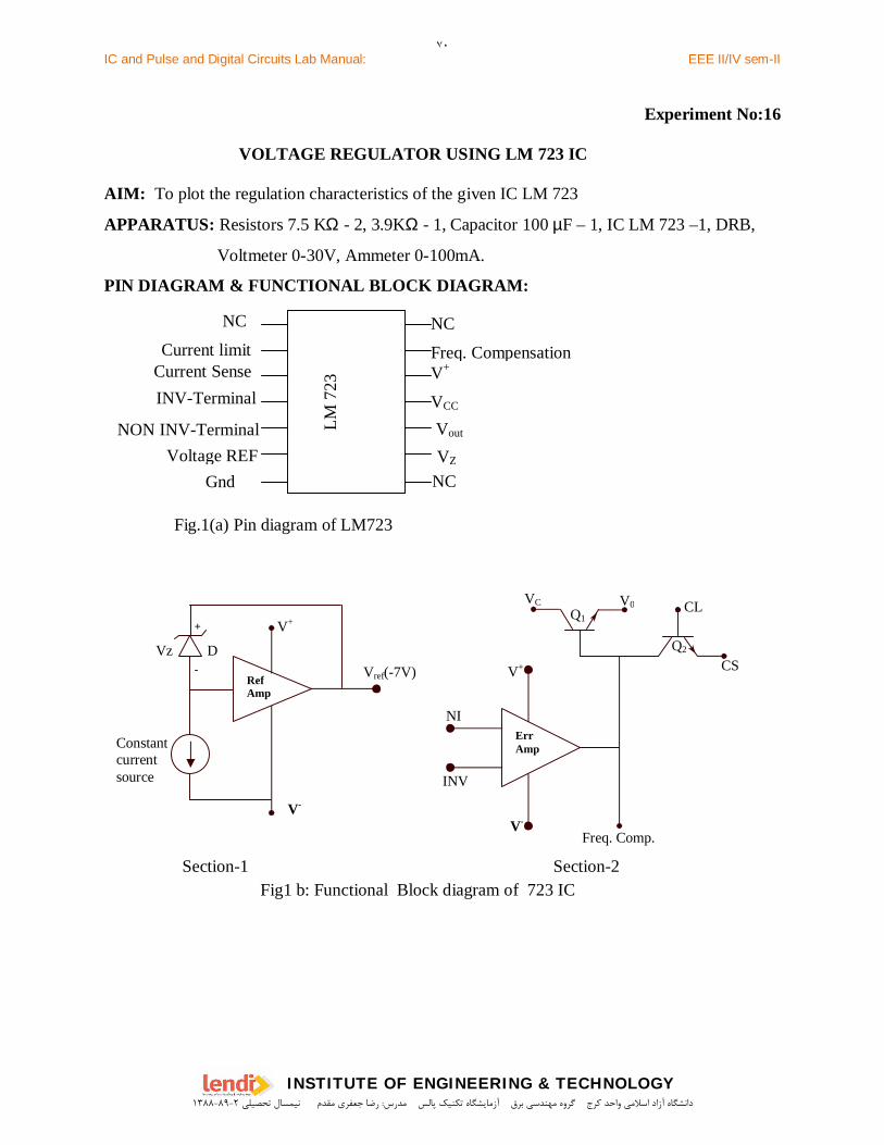
IC and Pulse and Digital Circuits Lab Manual: EEE II/IV sem-II
INSTITUTE OF ENGINEERING & TECHNOLOGY
NC
Current limitCurrent SenseINV-Terminal
NON INV-TerminalVoltage REF
Gnd
NC
NC
Freq. CompensationV+
VCC
Vout
VZ
Experiment No:16
VOLTAGE REGULATOR USING LM 723 IC
AIM: To plot the regulation characteristics of the given IC LM 723
APPARATUS: Resistors 7.5 KΩ - 2, 3.9KΩ - 1, Capacitor 100 µF – 1, IC LM 723 –1, DRB,
Voltmeter 0-30V, Ammeter 0-100mA.
PIN DIAGRAM & FUNCTIONAL BLOCK DIAGRAM:
Fig.1(a) Pin diagram of LM723
LM 7
23
RefAmp
Vz
+
Vref(-7V)-
V+
V-
Constantcurrentsource
D
Section-1
ErrAmp
NI
INV
V+
V-
VC V0Q1
Q2
CL
CS
Freq. Comp.
Section-2Fig1 b: Functional Block diagram of 723 IC
۷۰
دانشگاه آزاد اسالمي واحد كرج گروه مهندسي برق آزمايشگاه تكنيك پالس مدرس: رضا جعفري مقدم نيمسال تحصيلي 1۳۸۸-۸9-2
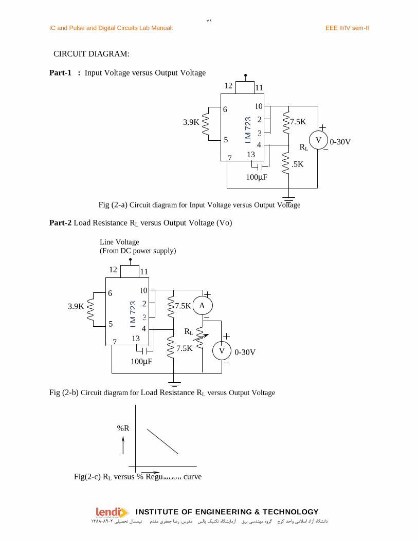
IC and Pulse and Digital Circuits Lab Manual: EEE II/IV sem-II
INSTITUTE OF ENGINEERING & TECHNOLOGY
CIRCUIT DIAGRAM:
Part-1 : Input Voltage versus Output Voltage
Fig (2-a) Circuit diagram for Input Voltage versus Output Voltage
Part-2 Load Resistance RL versus Output Voltage (Vo)
Fig (2-b) Circuit diagram for Load Resistance RL versus Output Voltage
Fig(2-c) RL versus % Regulation curve
12 11
6
5
102
34
7 13
100µF
A
V
LM 7
23
RL
3.9K 7.5K
7.5K 0-30V
Line Voltage(From DC power supply)R
12 11
6
5
102
34
7 13
100µF
LM 7
23
RL
3.9K 7.5K
.5K
0-30VV
%R
۷۱
دانشگاه آزاد اسالمي واحد كرج گروه مهندسي برق آزمايشگاه تكنيك پالس مدرس: رضا جعفري مقدم نيمسال تحصيلي 1۳۸۸-۸9-2
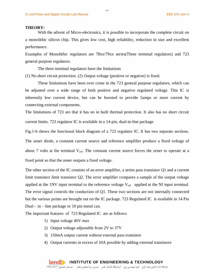
IC and Pulse and Digital Circuits Lab Manual: EEE II/IV sem-II
INSTITUTE OF ENGINEERING & TECHNOLOGY
THEORY: With the advent of Micro-electronics, it is possible to incorporate the complete circuit on
a monolithic silicon chip. This gives low cost, high reliability, reduction in size and excellent
performance.
Examples of Monolithic regulators are 78xx/79xx series(Three terminal regulators) and 723
general purpose regulators.
The three terminal regulators have the limitations
(1) No short circuit protection. (2) Output voltage (positive or negative) is fixed.
These limitations have been over come in the 723 general purpose regulators, which can
be adjusted over a wide range of both positive and negative regulated voltage. This IC is
inherently low current device, but can be boosted to provide 5amps or more current by
connecting external components.
The limitations of 723 are that it has no in built thermal protection. It also has no short circuit
current limits. 723 regulator IC is available in a 14-pin, dual-in-line package.
Fig.1-b shows the functional block diagram of a 723 regulator IC. It has two separate sections.
The zener diode, a constant current source and reference amplifier produce a fixed voltage of
about 7 volts at the terminal Vref. The constant current source forces the zener to operate at a
fixed point so that the zener outputs a fixed voltage.
The other section of the IC consists of an error amplifier, a series pass transistor Q1 and a current
limit transistor limit transistor Q2. The error amplifier compares a sample of the output voltage
applied at the 1NV input terminal to the reference voltage Vref applied at the NI input terminal.
The error signal controls the conduction of Q1. These two sections are not internally connected
but the various points are brought out on the IC package. 723 Regulated IC is available in 14 Pin
Dual – in – line package or 10 pin metal can.
The important features of 723 Regulated IC are as follows:
1) Input voltage 40V max
2) Output voltage adjustable from 2V to 37V
3) 150mA output current without external pass transistor
4) Output currents in excess of 10A possible by adding external transistors
۷۲
دانشگاه آزاد اسالمي واحد كرج گروه مهندسي برق آزمايشگاه تكنيك پالس مدرس: رضا جعفري مقدم نيمسال تحصيلي 1۳۸۸-۸9-2
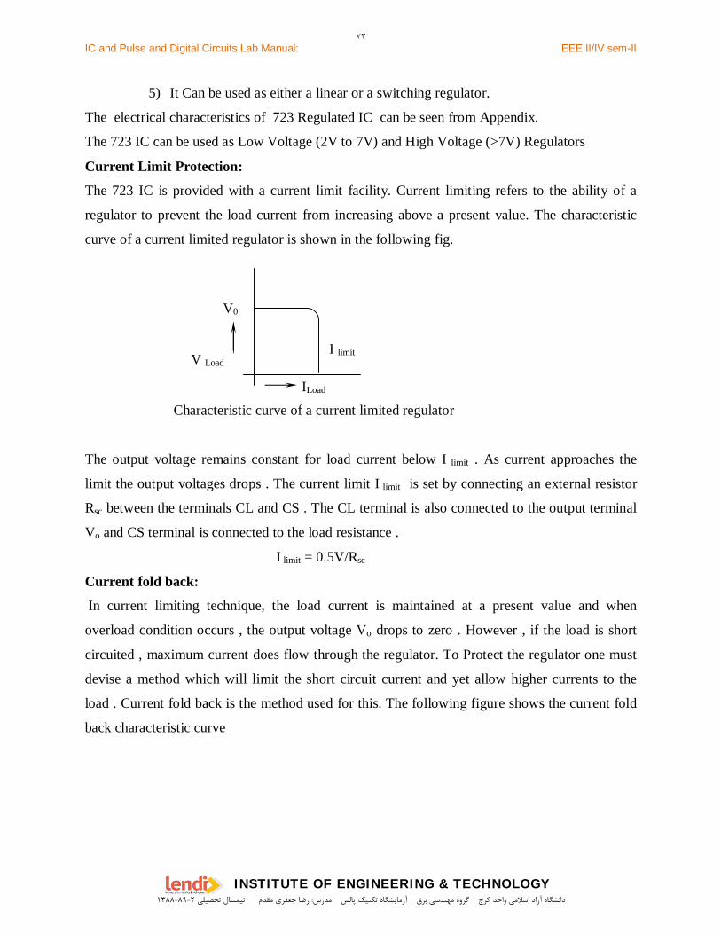
IC and Pulse and Digital Circuits Lab Manual: EEE II/IV sem-II
INSTITUTE OF ENGINEERING & TECHNOLOGY
5) It Can be used as either a linear or a switching regulator.
The electrical characteristics of 723 Regulated IC can be seen from Appendix.
The 723 IC can be used as Low Voltage (2V to 7V) and High Voltage (>7V) Regulators
Current Limit Protection:
The 723 IC is provided with a current limit facility. Current limiting refers to the ability of a
regulator to prevent the load current from increasing above a present value. The characteristic
curve of a current limited regulator is shown in the following fig.
Characteristic curve of a current limited regulator
The output voltage remains constant for load current below I limit . As current approaches the
limit the output voltages drops . The current limit I limit is set by connecting an external resistor
Rsc between the terminals CL and CS . The CL terminal is also connected to the output terminal
Vo and CS terminal is connected to the load resistance .
I limit = 0.5V/Rsc
Current fold back:
In current limiting technique, the load current is maintained at a present value and when
overload condition occurs , the output voltage Vo drops to zero . However , if the load is short
circuited , maximum current does flow through the regulator. To Protect the regulator one must
devise a method which will limit the short circuit current and yet allow higher currents to the
load . Current fold back is the method used for this. The following figure shows the current fold
back characteristic curve
V0
ILoad
V LoadI limit
۷۳
دانشگاه آزاد اسالمي واحد كرج گروه مهندسي برق آزمايشگاه تكنيك پالس مدرس: رضا جعفري مقدم نيمسال تحصيلي 1۳۸۸-۸9-2
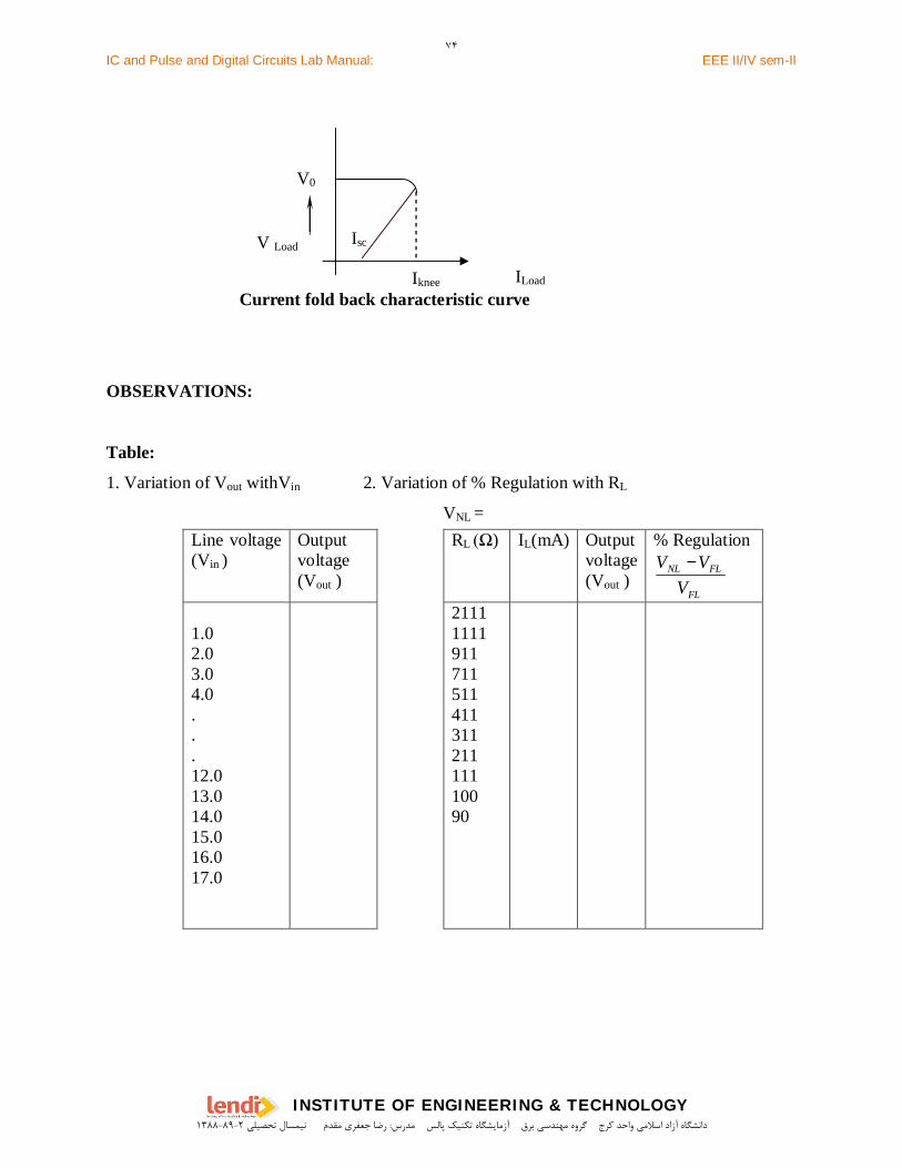
IC and Pulse and Digital Circuits Lab Manual: EEE II/IV sem-II
INSTITUTE OF ENGINEERING & TECHNOLOGY
Isc
Current fold back characteristic curve
OBSERVATIONS:
Table:
1. Variation of Vout withVin 2. Variation of % Regulation with RL
VNL =Line voltage(Vin )
Outputvoltage(Vout )
RL ) IL(mA) Outputvoltage(Vout )
% Regulation
FL
FLNL
VVV −
1.02.03.04.0...12.013.014.015.016.017.0
2111111191171151141131121111110090
V0
ILoad
V Load
Iknee
۷۴
دانشگاه آزاد اسالمي واحد كرج گروه مهندسي برق آزمايشگاه تكنيك پالس مدرس: رضا جعفري مقدم نيمسال تحصيلي 1۳۸۸-۸9-2

IC and Pulse and Digital Circuits Lab Manual: EEE II/IV sem-II
INSTITUTE OF ENGINEERING & TECHNOLOGY
PROCEDURE:
Part 1: Input Voltage versus Output Voltage
1. Connect the circuit as shown in the fig2-a.
2. Connect the supply between 12 & 7 terminals
3. Connect the voltmeter to 10 & ground terminals
4. Increase the input voltage and note down the corresponding output voltage
5. Initially the output voltage is increasing with an increase in input Voltage
At some value of input Voltage , the output voltage becomes constant
Note down all these readings from the multimeter.
6. Draw the Graph between the line voltage(Vin ) Versus output voltage( Vout )
Part 2: Load Resistance RL versus Output Voltage (Vo)
1. Connect the circuit as shown in the fig 2-b.
2. Keep the voltage constant at which part 1 is obtained.
3. Keep the load resistance (DRB) in the maximum position
( keep all the Knobs of DRB in maximum position)
4. Decrease the load resistance (RLoad) and note down the output current (ILoad)and output
voltage.
5. Decrease the load resistance till the output current reaches maximum rated current and
note down the corresponding values of the output voltage.
6. Draw the Graph between the load resistance(RLoad) and % regulation
RESULT:
Hence the output voltage of 723 regulator is observed for different input voltages . and the
characteristics of the IC LM 723 are plotted.
CONCLUSIONS :
It is concluded that the % regulation is decreased with an increase in the load resistance(RLoad )
۷۵
دانشگاه آزاد اسالمي واحد كرج گروه مهندسي برق آزمايشگاه تكنيك پالس مدرس: رضا جعفري مقدم نيمسال تحصيلي 1۳۸۸-۸9-2
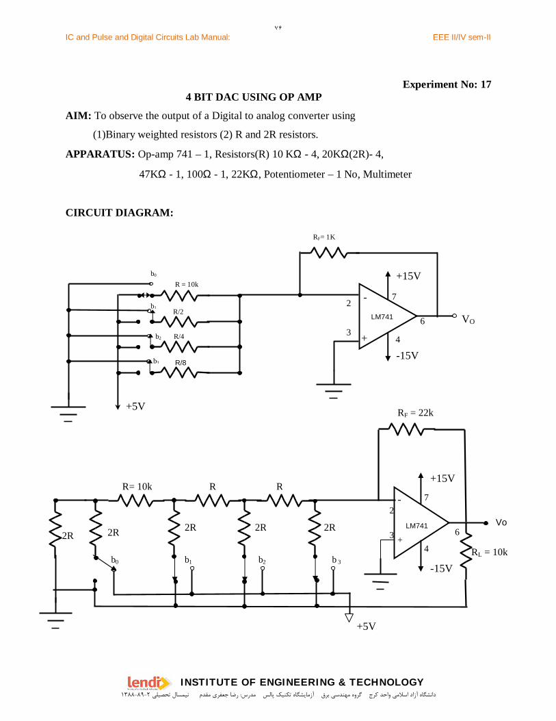
IC and Pulse and Digital Circuits Lab Manual: EEE II/IV sem-II
INSTITUTE OF ENGINEERING & TECHNOLOGY
Experiment No: 17 4 BIT DAC USING OP AMP
AIM: To observe the output of a Digital to analog converter using
(1)Binary weighted resistors (2) R and 2R resistors.
APPARATUS: Op-amp 741 – 1, Resistors(R) 10 KΩ - 4, 20KΩ(2R)- 4,
47KΩ - 1, 100Ω - 1, 22KΩ, Potentiometer – 1 No, Multimeter
CIRCUIT DIAGRAM:
+
-
Vo
R= 10k
b0
+5V
+15V
-15V
2
3
7
4
6LM741
R R
2R 2R 2R 2R2R
b1 b2 b 3
RF = 22k
RL = 10k
+
-
+15V
-15V
VO
R = 10k
R/4
R/2
R/8
b0
b1
b2
b3
+5V
LM741
2
3
7
4
6
RF= 1K
۷۶
دانشگاه آزاد اسالمي واحد كرج گروه مهندسي برق آزمايشگاه تكنيك پالس مدرس: رضا جعفري مقدم نيمسال تحصيلي 1۳۸۸-۸9-2

IC and Pulse and Digital Circuits Lab Manual: EEE II/IV sem-II
INSTITUTE OF ENGINEERING & TECHNOLOGY
THEORY:
A Digital-to-Analog Converter is used when a Binary output from a digital system must be
converted to some equivalent Analog voltage or Current.The Binary output from a digital system
is difficult to interpret.However a DAC makes the interpretation easier.The function of DAC is
exactly opposite to that of ADC.
Advantages:1)It is simpler in construction when compared to ADC 2)It can be used to form the
ADC.
Types of D/A Converters:
There are two types of DACs available
1. D/A converter with Binary –weighted Resistors
2. D/A converter with R and 2R resistors.
i.e.,A D/A converter in its simplest form uses an op-amp and either binary weighted resistors or
R and 2R resistors.
1) D/A converter with Binary –weighted Resistors
Basic DAC Techniques: The schematic of a DAC is shown in Fig1. The input is an n-bit binary
word D and is combined with a reference voltage VR to give an analog output signal. The output
of a DAC can be either a voltage or current. Theory o/p voltage
V0 = K VFS (b12-1+b22-2+…..+bn2-n) Eq-1
Where V0 = output voltage
VFS = full scale output voltage
K = scaling factor usually adjusted to unity
b1b2…..bn = n-bit binary fractional word with the decimal point located at the left
b1 = most significant bit (MSB) with a weight of VFS/2
bn = least significant bit (LSB) with a weight of VFS/2n
۷۷
دانشگاه آزاد اسالمي واحد كرج گروه مهندسي برق آزمايشگاه تكنيك پالس مدرس: رضا جعفري مقدم نيمسال تحصيلي 1۳۸۸-۸9-2
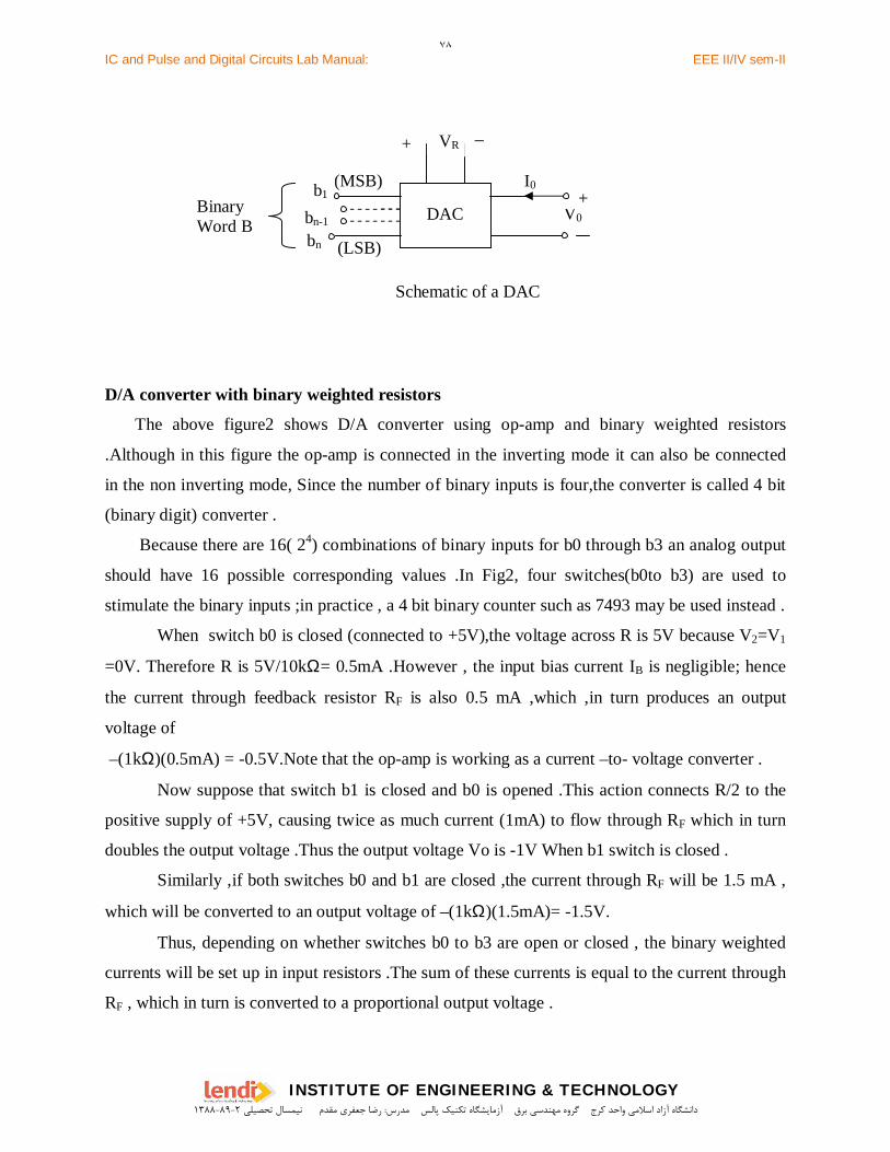
IC and Pulse and Digital Circuits Lab Manual: EEE II/IV sem-II
INSTITUTE OF ENGINEERING & TECHNOLOGY
D/A converter with binary weighted resistors
The above figure2 shows D/A converter using op-amp and binary weighted resistors
.Although in this figure the op-amp is connected in the inverting mode it can also be connected
in the non inverting mode, Since the number of binary inputs is four,the converter is called 4 bit
(binary digit) converter .
Because there are 16( 24) combinations of binary inputs for b0 through b3 an analog output
should have 16 possible corresponding values .In Fig2, four switches(b0to b3) are used to
stimulate the binary inputs ;in practice , a 4 bit binary counter such as 7493 may be used instead .
When switch b0 is closed (connected to +5V),the voltage across R is 5V because V2=V1
=0V. Therefore R is 5V/10kΩ= 0.5mA .However , the input bias current IB is negligible; hence
the current through feedback resistor RF is also 0.5 mA ,which ,in turn produces an output
voltage of
–(1kΩ)(0.5mA) = -0.5V.Note that the op-amp is working as a current –to- voltage converter .
Now suppose that switch b1 is closed and b0 is opened .This action connects R/2 to the
positive supply of +5V, causing twice as much current (1mA) to flow through RF which in turn
doubles the output voltage .Thus the output voltage Vo is -1V When b1 switch is closed .
Similarly ,if both switches b0 and b1 are closed ,the current through RF will be 1.5 mA ,
which will be converted to an output voltage of –(1kΩ)(1.5mA)= -1.5V.
Thus, depending on whether switches b0 to b3 are open or closed , the binary weighted
currents will be set up in input resistors .The sum of these currents is equal to the current through
RF , which in turn is converted to a proportional output voltage .
DAC
+
V0 +
_VR
(MSB)
(LSB)
b1
bn-1
Schematic of a DAC
BinaryWord B
I0
bn
۷۸
دانشگاه آزاد اسالمي واحد كرج گروه مهندسي برق آزمايشگاه تكنيك پالس مدرس: رضا جعفري مقدم نيمسال تحصيلي 1۳۸۸-۸9-2
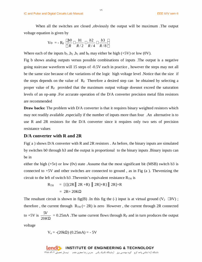
IC and Pulse and Digital Circuits Lab Manual: EEE II/IV sem-II
INSTITUTE OF ENGINEERING & TECHNOLOGY
When all the switches are closed ,obviously the output will be maximum .The output
voltage equation is given by
Vo = - RF
+++
8/3
4/2
2/10
Rb
Rb
Rb
Rb
Where each of the inputs b3 ,b2 ,b1 and b0 may either be high (+5V) or low (0V).
Fig b shows analog outputs versus possible combinations of inputs .The output is a negative
going staircase waveform will 15 steps of -0.5V each in practice , however the steps may not all
be the same size because of the variations of the logic high voltage level .Notice that the size if
the steps depends on the value of RF Therefore a desired step can be obtained by selecting a
proper value of RF provided that the maximum output voltage doesnot exceed the saturation
levels of an op-amp .For accurate operation of the D/A converter precision metal film resistors
are recommended
Draw backs: The problem with D/A converter is that it requires binary weighted resistors which
may not readily available ,especially if the number of inputs more than four .An alternative is to
use R and 2R resistors for the D/A converter since it requires only two sets of precision
resistance values
D/A converter with R and 2RFig( a ) shows D/A converter with R and 2R resistors . As before, the binary inputs are simulated
by switches b0 through b3 and the output is proportional to the binary inputs .Binary inputs can
be in
either the high (+5v) or low (0v) state .Assume that the most significant bit (MSB) switch b3 is
connected to +5V and other switches are connected to ground , as in Fig (a ). Thevenizing the
circuit to the left of switch b3 .Thevenin’s equivalent resistance RTH is
RTH = [[(2R 2R +R) 2R]+R 2R]+R
= 2R= 20KΩ
The resultant circuit is shown in fig(B) .In this fig the (-) input is at virtual ground (V2 ≅0V) ;
therefore , the current through RTH (= 2R) is zero However , the current through 2R connected
to +5V isΩK
V20
5 = 0.25mA .The same current flows through RF and in turn produces the output
voltage
Vo = -(20kΩ) (0.25mA) = - 5V
۷۹
دانشگاه آزاد اسالمي واحد كرج گروه مهندسي برق آزمايشگاه تكنيك پالس مدرس: رضا جعفري مقدم نيمسال تحصيلي 1۳۸۸-۸9-2

IC and Pulse and Digital Circuits Lab Manual: EEE II/IV sem-II
INSTITUTE OF ENGINEERING & TECHNOLOGY
Using the same analysis, the output voltage corresponding to all possible combinations of binary
inputs can be calculated .The maximum or full –scale output of -9.375 V is obtained when all
the inputs are high .The output voltage equation can be written as
Vo = - RF
+++
Rb
Rb
Rb
Rb
160
81
42
23
Where each of the inputs b3, b2, b1 and b0 may be either high(+5V) or low (0V)
The great advantage of the D/A Converter is that it requires only two sets of precision
resistance values; nevertheless, it requires more resistors and is also more difficult to analyze
than the binary –weighted resistor type .As the number of binary inputs is increased beyond four,
both D/A converter circuit get complex and their accuracy degenerates. Therefore, in critical
applications an integrated circuit specially designed as D/A converter should be used.
OBSERVATIONS
S.No Digital Inputs Analog Output
1 0 0 0 0
2 0 0 0 1
3 0 0 1 0
4 0 0 1 1
5 0 1 0 0
6 0 1 0 1
7 0 1 1 0
8 0 1 1 1
9 1 0 0 0
10 1 0 0 1
11 1 0 1 0
12 1 0 1 1
13 1 1 0 0
14 1 1 0 1
15 1 1 1 0
16 1 1 1 1
۸۰
دانشگاه آزاد اسالمي واحد كرج گروه مهندسي برق آزمايشگاه تكنيك پالس مدرس: رضا جعفري مقدم نيمسال تحصيلي 1۳۸۸-۸9-2

IC and Pulse and Digital Circuits Lab Manual: EEE II/IV sem-II
INSTITUTE OF ENGINEERING & TECHNOLOGY
PROCEDURE:
1. Connect the circuit as shown in the diagram.
2. Connect the output of ladder to the input of op-amp 741 ,
3. Observe the output of op-amp 741 with DMM.
4. For each value of input variation measure the output voltage with DMM and tabulate
the values.
5. Now remove DMM and observe the output on CRO.
6. Check whether the output of amplifier is a staircase waveform.
RESULT: Operation of digital to analog converter is verified.
۸۱
دانشگاه آزاد اسالمي واحد كرج گروه مهندسي برق آزمايشگاه تكنيك پالس مدرس: رضا جعفري مقدم نيمسال تحصيلي 1۳۸۸-۸9-2