Embed Size (px)
Citation preview

30
International Journal of Computing and ICT Research, Vol. 4, No. 1, June 2010
Experiments for Accelerating IEEE 802.11i on Cyclone II FPGA
Chakib Alaoui, Ph.D‡. Taif University, KSA
Abstract
This paper presents hardware solutions for accelerating IEEE 802.11i. Several experiments were applied on the low-cost Cyclone II FPGA by using various architectures with different number of threads. The FPGA offloads the process of AES encryption from the master CPU. In addition, it offers the possibility of using several threads to run the AES encryption. Different optimizations have been applied on the hardware architecture of AES and on the basic unit of AES, in order to satisfy different constraints in terms of latency, area occupation and speed. Their performances are compared to AES software implemented on a NIOS II processor. A strong focus is devoted for the achievement of high throughput, which is required to support security requirements for the high bandwidth applications.
Categories and Subject Descriptors: B.2.4 [Algorithms], B.6.1 [Memory Used as Logic], B.7.1 [Algorithms Implemented in Hardware], C.1.4 [Parallel Architectures]. General Terms: IEEE 802.11i, AES, Cipher, WEP, FPGA. CYCLONE II
IJCIR Reference Format:
Chakib Alaoui, Experiments for Accelerating IEEE 802.11i on Cyclone II FPGA. International Journal of Computing and ICT Research, Vol. 4, No. 1, pp. 30 - 42. http://www.ijcir.org/volume4-number1/article 4.pdf.
______________________________________________________________________________________ 1. INTRODUCTION ENCRYPTION is a fundamental building block for data and telecommunication networks security. It makes electronic commerce, payment systems and transactions over networks possible. It is also a tool for privacy, trust, access control and corporate security, as defined by NIST [2001]. Effective implementations of cryptographic algorithms are essential for the realization of many real time communication systems. Performance has always been one of the most critical issues of a cryptographic function. It determines its effectiveness. It is evaluated by many metrics like latency, size and power consumption. Cryptographic computations are intensive and therefore they influence the performance of the whole system.
Wi-Fi (IEEE 802.11) is a common example of wireless communication. Schools, hospitals and public buildings are the major applications fields. However, the major drawback of current wireless LAN technology is the weak security measures in the standard 802.11 protocols (Wired Equivalent Privacy -WEP) as described by Graham S. J. [2003]. The solutions for WLAN security are delivered in two stages:
‡ Author’s Address: Chakib Alaoui, Faculty of Computers and Information Systems. Taif University. Taif – Al-Haweiah – P.O. Box
888 – Zip Code 21974 – Kingdom of Saudi Arabia – www.tu.edu.sa.
"Permission to make digital or hard copies of part or all of this work for personal or classroom use is granted without fee provided that
copies are not made or distributed for profit or commercial advantage and that copies bear this notice and the full citation on the first
page. Copyrights for components of this work owned by others than IJCIR must be honored. Abstracting with credit is permitted. To
copy otherwise, to republish, to post on servers or to redistribute to lists, requires prior specific permission and/or a fee."
© International Journal of Computing and ICT Research 2010.
International Journal of Computing and ICT Research, ISSN 1818-1139 (Print), ISSN 1996-1065 (Online), Vol.4, No.1, pp. 30 - 42,
June, 2010

31
International Journal of Computing and ICT Research, Vol. 4, No. 1, June 2010
o The first is the Wi-Fi Protected Access (WPA), which has been designed to allow software upgrade for existing WLAN systems.
o The second is the standard IEEE 802.11i, which provides the best available security, but requires hardware support as described by Graham S. J. [2003].
The AES (Advanced Encryption Standard) protocol requires complex algorithms for encryption/decryption processes, which makes them computationally extensive (AES requires about 350 lines of code, WEP implement RC4 algorithm that require 50 lines of code). At backbone communication channels or heavily loaded servers, it is possible to lose processing speed. This drops the efficiency of the overall system while running cryptography algorithms. Moreover, the 802.11i standard specifies that AES should have its own coprocessor in order to speed up the encryption/decryption process (Morioka et al. [2002]). This implies that older existing wireless hardware cannot be upgraded via firmware to support IEEE 802.11i.
IEEE 802.11i (also known as WPA2) is an enhancement of the 802.11 standard specifying security mechanisms of wireless networks. The draft standard was ratified on June 24, 2004, and supersedes the previous security specifications. In addition to the introduction of key management and establishment, it defines encryption and authentication improvement (Morioka et al. [2002]). AES is a mandatory implementation of 802.11i. It was designed by D. Whiting, N. Ferguson and R. Housley. AES may be implemented in sizes of 128 bits, 192 bits or 256 bits, but 802.11i supports 128 bit AES only. There are several AES implementation on FPGA’s (Field Programmable Gate Arrays) available on the literature as was described by Alireza et al. [2004], Chodowiec et al. [2001], Chiueh et al. [2000], Dandalis et al. [2000], Elbirt et al. [2000], Elbirt A. J. et al. [2001], Gaj et al. [2000], Fisher V. et al. [2001], Ichikawa et al. [2000] and McLoone et al. [2001]. Its ASIC (Application Specific Integrated Circuit) counterpart was also widely studied by Lin et al. [2001], Lutz et al. [2002], Mayer et al. [2002], Morioka et al.[2002] and Morioka et al. [2000]. These implementations feature high speed and high costs suitable for high end applications only. Early AES designs featured pipelined architectures and limited resource utilization. These designs were described by Dandalis et al. [2000], Elbirt et al. [2000], Gaj et al. [2000] and Ichikawa et al. [2000]. Later FPGA and ASIC implementations showed better optimization, using dedicated on-chip memories implementing S-Boxes, as described in Alireza et al. [2004], Chiueh et al. [2000], Edney et al. [2003], Hodjat A. et al. [2004], Lin et al. [2001], Kimmo et al. [2003] and Verbauwhede I. et al. [2003].
The goal of this work is to design and evaluate an embedded coprocessor based on the NIOS II processor. It implements an efficient, cost-effective solution and optimized WiFi NIC (Network Interface Card). Different optimizations will be applied on the hardware architecture in order to satisfy different constrains in terms of latency, area occupation and security. This design uses Cyclone II FPGA (Field Programmable Gate Array) using Quartus foundation series.
2. IEEE 802.11i NETWORK INTERFACE CARD ARCHITECTURE 2.1 Network Interface Card components in IEEE 802.11 There are essentially four parts in a Wi-Fi LAN card shown in figure 1:
32
International Journal of Computing and ICT Research, Vol. 4, No. 1, June 2010
Figure1: NIC components in IEEE 802.11
1. Radio Frequency (RF) deals with the transmission and reception of the signal through the antenna. 2. MODEM extracts data from the received signal 3. Medium Access Control (MAC) is the heart of IEEE802.11 protocol. It has many functions like encryption/decryption of data, retransmission of lost data and data acknowledgement. 4. Host Interface is used to connect all the above to a computer like the USB or PCI bus.
Since IEEE 802.11i protocol is an enhancement to the MAC in terms of security, a closer look at the MAC components of IEEE802.11 is needed. Refer to figure 2.
Figure 2: MAC Components Graham S. J. [2003] MAC is made of a microprocessor who handles all the formatting and timing operations to control the protocol, the firmware is software that implements most functions and finally a hardware assist that speeds up the process of encryption/decryption of WEP. The hardware assist implemented in the existing NIC causes a critical problem for IEEE 802.11i; it cannot support AES. 2.2 WIFI Adapter Card IEEE 802.11i
2.2.1 WIFI Adapter Card IEEE 802.11i Block Diagram
The earlier NIC is static hardware and therefore its configuration could not be changed. The new design overcomes this issue and gives more flexibility for the longer term. FPGAs provide hardware reconfiguration possibility, i.e. flexible interconnect and short development time. They are very suitable as

33
International Journal of Computing and ICT Research, Vol. 4, No. 1, June 2010
hardware accelerators for AES. Another great improvement of the new WiFi adapter card is the network processor. It controls and processes all the network tasks so that the host CPU can be used for non-network related tasks such as video/audio processing. In this case, all networking tasks should be dropped into the FPGA (Encryption, Firewall, TCP|IP stack…). For evaluation purposes, NIOS II CPU from Altera Corporation was used as network processor. Figure 3 shows a block diagram of the WiFi adapter card 802.11i
Figure 3: WiFi Adapter Card IEEE 802.11i Avalon bus is an Altera’s interface bus, used in NIOS II CPU. RAM contains unencrypted or decrypted data ready to be processed by AES coprocessor. The ROM contains all instructions necessary for the FPGA to work. During the boot-up phase, instructions are fetched from ROM since FPGA is volatile. PCI Bridge provides transparency between the host CPU and the NIOS II network processor. MODEM and Radio Frequency are off-chip. 2.2.2 The Choice of Network Processor
It was shown by Evangelos et al. [2001] that performance improvements made to general purpose processors do not translate necessarily into improved network performance, because these processors are not optimized for network data processing. Recent processors incorporates several innovations in their architecture, like larger caches, out of order executions, deep pipelines, and super-scale executions, all of which cannot necessarily be exploited by networking code. It was also concluded by the same author, that, even if the processor speed increases by Moore’s law, network system speed increases in much lower pace. So it is necessary to develop an efficient co-processor dedicated for network tasks.
3. AES DESIGN AND IMPLEMENTATION
3.1 Key Scheduling by using Rijndael Algorithm

34
International Journal of Computing and ICT Research, Vol. 4, No. 1, June 2010
Figure 4: Algorithmic View of AES 128 from Zambreno et al. [2004] The initial 128-bit key is fed into the KeyExpansion function which produces separate keys for each of the 10 required rounds. These rounds combine their scheduled keys with a two dimensional representation of the input using various transformations:
o SubBytes( ) calculates a non-linear function independently on each byte of the state. The substitution used by this transformation can be more simply represented as a lookup table which is referred to as an “S-box”.
o MixColumns( ) separately modifies each column of the state in what is essentially a matrix multiplication operation. Fortunately, in the 8-bit finite mathematical field relied on by this class of block ciphers, multipliers can be replaced with simpler fixed-length shifts and XOR operations.
o ShiftRows( ) cyclically shifts the bytes in the last three rows of the state. As this function requires no computational hardware it can be implemented on an FPGA as simple wiring.
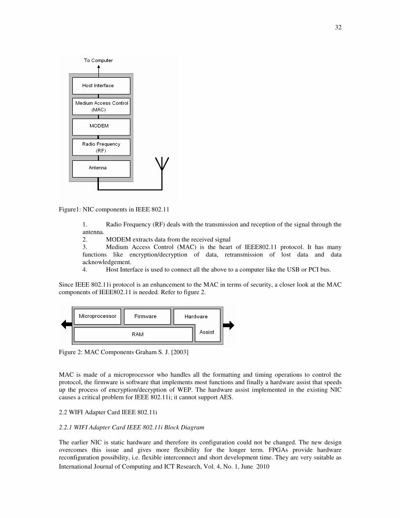
o AddRoundKey( ) adds the round key to the state using a bitwise XOR operation. Key scheduling expands a 128-bit cipher key into a 170 Byte key. It utilizes operations like word rotation, word substitution, and exclusive OR with round constant. Figure 5, from A. SATOH [2001], shows a more detailed AES key scheduling architecture.
35
International Journal of Computing and ICT Research, Vol. 4, No. 1, June 2010
Figure 5: Detailed Key Scheduling Architecture. The key expander in Figure 5 generates 11 sets of 128-bit round keys from one 128-bit secret key by using a 4-byte S-Box. These round keys can be prepared on the fly in parallel with the encryption process. In the decryption process, these sets of keys are used in reverse order.
First, the 128 bit cipher is divided into 4 sub-keys Word[0] to Word[3]. Then the shown operations are done to produce four new sub-keys Word[4] to Word[7]. Then this cycle is repeated 10 times in order to produce 160 Bytes. In total, a key of 176 Bytes is obtained.
In order to produce the new four sub-keys, the previous values of sub-keys are needed. So with this architecture, parallel execution is not possible.
In order to exploit the nature of parallelism offered by the FPGA hardware, an improved architecture is proposed using redundant computations. Refer to figure 6.
Figure 6: Modified Key Scheduling Architecture

36
International Journal of Computing and ICT Research, Vol. 4, No. 1, June 2010
3.2 AES Hardware Architecture
Figure 7: AES( ) Architecture Figure 7 shows the AES() architecture, it is made of: Control Unit: controls the components of the core (key registers bank and AES core). It also organizes the data flow by loading the specific data at the right round. After 10 rounds, the control unit will force the AES core to stop and output the cipher text. Key registers bank: outputs the round keys. These sub-keys were computed offline. AES Core: performs all the AES( ) modules described before.
3.3 Round Component Optimizations Four different hardware/software optimizations have been developed. The first is based on the basic AES( ) unit which implements one round and executes ten times. This optimization employs the minimum hardware. The second optimization uses two AES( ) units and executes 5 times. The third implementation uses five AES( ) unites and executes them two times. Finally, the fourth implementation uses ten AES( ) units and executes them only one time. This last optimization uses the maximum hardware. Figure 8 shows the four different AES implementations.

37
International Journal of Computing and ICT Research, Vol. 4, No. 1, June 2010
Figure 8: Four Different AES Implementations: 1 AES() x 10 exec., 2 AES x 5 exec., 5 AES x 2 exec. and 10 AES x 1 exec.
38
International Journal of Computing and ICT Research, Vol. 4, No. 1, June 2010
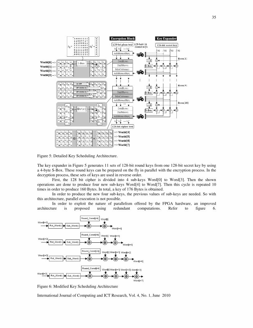
4. AES TESTING AND EVALUATION The code has been synthesized using Altera’s Quartus 6.1 development system. And Altera’s Cyclone II chip was chosen for the implementation of the ciphers, because of its good performance among Altera’s family and low cost. 4.1 AES Modules Synthesis Table 1 shows the synthesis of the main components of AES, which are MixColumns() ver1, MixColumns() ver2, ShiftRows(), SubBytes() and SubBytes that implements RAM. TABLE1: SYNTHESIS OF THE MAIN COMPONENTS OF AES There are two choices SubBytes() look-up table in the target device: RAM: The values of the S-Box are loaded at the embedded RAM at configuration time. Logic: S-Box can also be converted into logical representations and therefore implemented with logic elements. This option consumes chip area.
Data from table1 shows that the implementation of SubBytes() with embedded RAM gives significant improvements in the area/delay performance. Each 8 bits require 2048 bit of RAM, so in order to process 128 bits, 32768 bits for a 16x16 S-Box. 4.2 AES Cores Synthesis Table 2 shows the synthesis results of AES key scheduling in Cyclone II TABLE2: SYNTHESIS RESULTS OF AN AES KEY SCHEDULING WITH CYCLONE II
Implementation Total
Logic Elements 1102 Registers 269 Clock Frequency (MHz) 167.81 Clock Cycles per Block 11 Period (ns) 5.96 Throughput (Mbits/s) 1952.7
Table 3 shows the synthesis results of AES without exploring the embedded RAM in Cyclone II
Total MixColumns() ver1
MixColumns() ver2
SubBytes() SybBytes() RAM
Logic Elements 212 196 196 0
Registers 0 0 0 0
Memory bits 0 0 0 2048
Cell Delay (ns) 4.275 4.446 5.777 4.292
Interconnect
Delay (ns)
11.263 11.394 9.090 7.955
Worst Case tpd
(ns)
15.538 15.840 14.867 14.04
39
International Journal of Computing and ICT Research, Vol. 4, No. 1, June 2010
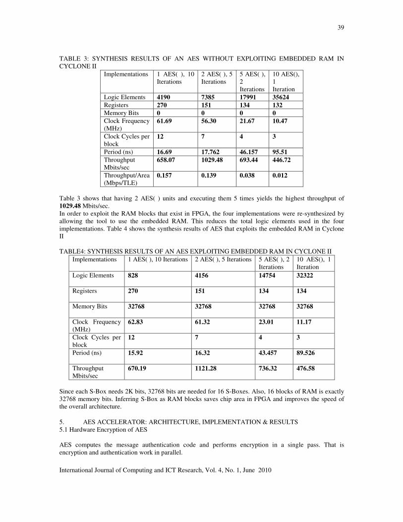
TABLE 3: SYNTHESIS RESULTS OF AN AES WITHOUT EXPLOITING EMBEDDED RAM IN CYCLONE II
Implementations 1 AES( ), 10 Iterations
2 AES( ), 5 Iterations
5 AES( ), 2 Iterations
10 AES(), 1 Iteration
Logic Elements 4190 7385 17991 35624
Registers 270 151 134 132
Memory Bits 0 0 0 0
Clock Frequency (MHz)
61.69 56.30 21.67 10.47
Clock Cycles per block
12 7 4 3
Period (ns) 16.69 17.762 46.157 95.51
Throughput Mbits/sec
658.07 1029.48 693.44 446.72
Throughput/Area (Mbps/TLE)
0.157 0.139 0.038 0.012
Table 3 shows that having 2 AES( ) units and executing them 5 times yields the highest throughput of 1029.48 Mbits/sec. In order to exploit the RAM blocks that exist in FPGA, the four implementations were re-synthesized by allowing the tool to use the embedded RAM. This reduces the total logic elements used in the four implementations. Table 4 shows the synthesis results of AES that exploits the embedded RAM in Cyclone II TABLE4: SYNTHESIS RESULTS OF AN AES EXPLOITING EMBEDDED RAM IN CYCLONE II
Implementations 1 AES( ), 10 Iterations 2 AES( ), 5 Iterations 5 AES( ), 2 Iterations
10 AES(), 1 Iteration
Logic Elements 828 4156 14754 32322
Registers 270 151 134 134
Memory Bits 32768 32768 32768 32768
Clock Frequency (MHz)
62.83 61.32 23.01 11.17
Clock Cycles per block
12 7 4 3
Period (ns) 15.92 16.32 43.457 89.526
Throughput Mbits/sec
670.19 1121.28 736.32 476.58
Since each S-Box needs 2K bits, 32768 bits are needed for 16 S-Boxes. Also, 16 blocks of RAM is exactly 32768 memory bits. Inferring S-Box as RAM blocks saves chip area in FPGA and improves the speed of the overall architecture.
5. AES ACCELERATOR: ARCHITECTURE, IMPLEMENTATION & RESULTS 5.1 Hardware Encryption of AES AES computes the message authentication code and performs encryption in a single pass. That is encryption and authentication work in parallel.

40
International Journal of Computing and ICT Research, Vol. 4, No. 1, June 2010
Figure 7 shows the AES algorithm used in the 802.11i security protocol. It is responsible for the authentication that produces a 64-bit long MIC (Message Integrity Check). IV in the Initialization Vector, it contains the source address, the length of packet during the session and other fields. PN: Packet Number.
Figure 9: AES Algorithm from McLoone et al. [2001] 5.2. AES Implementation Results In order to implement the AES core, the design that meets the lowest area with the highest throughput must be selected. The lowest area achieves a throughput of 670.19 Mbps (1 AES( ), 10 executions), while the second design (2 AES( ), 5 executions) achieves 1121.28 Mbps. Therefore these two different designs have been used to implement AES algorithm. Figure 10 shows the performance and the cost comparison of these 2 implementations.
Figure 10: Performance and Cost Comparison of AES Implementations

41
International Journal of Computing and ICT Research, Vol. 4, No. 1, June 2010
6. CONCLUSION In this paper a top-down methodology for implementing cryptographic block ciphers on FPGA was proposed and evaluated. Cyclone II series FPGA and NIOS II CPU make a low-cost and compact solution that adds high-speed features. Various architectures of AES units were implemented with strong emphasis on high speed performance. FPGA technology has matured to the point where high throughput can be easily obtained. The most interesting result achieved in this paper is a data rate of 688.16 Mbits/sec by using the standard and low cost Cyclon II FPGA chip of Altera. This encryption rate meets the performance requirements of the emerging cryptographic applications such as the high speed standard IEEE 802.11n which supports a data rate of 600 Mbps as supported by Evangelos et al. [2001]
7. REFERENCES
AKASHI SATOH, SUMIO MORIOKA, KOHJI TAKANO, AND SEIJI MUNETOH. A Compact Rijndael Hardware Architecture with S-Box Optimization. Proc. ASIACRYPT 2001, LNCS 2248, 2001, pp. 239–254.
ALIREZA HODJAT AND INGRID VERBAUWHEDE. 2004. A 21.54 Gbit/s Fully Pipelined AES Processor on FPGA. IEEE Symposium on Field Programmable Custom Computing Machines,
April 2004.
ALIZERA HODJAT AND INGRID VERBAUWHEDE. 2004. Minimum area Cost for a 30 to 70 Gbits/s AES Processor. Proceedings of IEEE Computer Society Annual Symposium on VLSI, Pages 83-88,
February 2004
CHODOWIEC P., GAJ K., BELLOWS P. AND SCHOTT B. 2001. Experimental Testing of the Gigabit IPSec-Compliant Implementations of Rijndael and Triple DES Using SLAAC-1V FPGA Accelerator Board. Information Security Conference (ISC 2001), Malaga, Spain, 2001
DANDALIS A., PRASANNA V.K. AND ROLIM J.D. 2000. A Comparative Study of Performance of AES Final Candidates Using FPGAs. Cryptographic Hardware and Embedded Systems Workshop
(CHES 2000), Worcester, Massachusetts, 2000
ELBIRT A.J., YIP W., CHETWYND B. AND PAAR C. 2000. An FPGA Implementation and Performance Evaluation of the AES Block Cipher Candidate Algorithm Finalists. Third Advanced
Encryption Standard (AES3) Candidate Conference, New York, 2000 ELBIRT A.J., YIP W., CHETWYND B. AND PAAR C. 2001. An FPGA-based performance evaluation of
the AES block cipher candidate algorithm finalists, IEEE Transactions on Very Large Scale
Integration (VLSI) Systems, Volume: 9 Issue: 4, August 2001 EVANGELOS P. MARKATOS. 2001. Speeding up TCP/IP: Faster Processors are not enough. The 21st
IEEE International Performance, Computing and Communication Conference, 2001
FISCHER V. AND DRUTAROVSKY M. 2001. Two Methods of Rijndael Implementation in Reconfigurable Hardware. Cryptographic Hardware and Embedded Systems (CHES 2001), Paris,
France, 2001
GAJ K. AND CHODOWIEC P. 2000. Comparison of the Hardware Performance of the AES Candidates Using Reconfigurable Hardware. Third Advanced Encryption Standard (AES3) Candidate
Conference, New York, 2000 ICHIKAWA T. AND MATSUI T. 2000. Hardware Evaluation of the AES Finalists. Third Advanced
Encryption Standard (AES3) Candidate Conference, New York, 2000
J. ZAMBRENO, D. NGUYEN AND A. N. CHOUDHARY, “Exploring area/delay tradeoffs in an AES FPGA implementation,” FPL 2004, LNCS3203, pp. 575-585, 2004.
JARVINEN K.U., TOMMISKA M.T. AND SKYTTA J.O. 2003. A Fully Pipelined Memoryless 17.8 Gbps AES-128 Encryptor, International Symposium on Field-Programmable Gate Arrays, Monterey,
CA, 2003
JON EDNEY, WILLIAM A. AND ARBAUGH. 2003. Real 802.11 Security: Wi-Fi Protected Access and 802.11i. ISBN 0-321-13620-9, Chap9, July 15, 2003
KIMMO U. JARVINEN, MATTI TOMMISKA AND SKYTTA J.O. 2003. A Fully Pipelined Memoryless 17.8 Gbps AES-128 Encryptor. Proceedings of the ACM/SIGDA International Symposium on
Field Programmable Gate Arrays, February 23-25 2003, Monterey, CA.

42
International Journal of Computing and ICT Research, Vol. 4, No. 1, June 2010
LIN T.F., SU C.P., HUANG C.T. AND WU C.W. 2001. A High-Throughput Low-Cost AES Cipher Chip. IEEE Asia-Pacific Conference on ASIC, 2002
LUTZ A.K., TREICHLER J., G¨URKAYNAK F.K., KAESLIN H., BASLER G., ERNI A., REICHMUTH S., ROMMENS P., OETIKER S. AND FICHTNER W. 2002. 2Gbit/s Hardware Realizations of RIJNDAEL and ERPENT: A Comparative Analysis. Cryptographic Hardware and Embedded
Systems (CHES 2002), San Francisco Bay, CA, 2002
MAYER U., OELSNER C. AND KOHLER T. 2002. Evaluation of Different Rijndael Implementations for High-end Servers. IEEE International Symposium on Circuits and Systems (ISCAS 2002), 2002
MCLOONE M. AND MCCANNY J.V. 2001. High Performance Single-Chip FPGA Rijndael Algorithm Implementations. Cryptographic Hardware and Embedded Systems (CHES 2001), Paris, France,
2001 MCLOONE M. AND MCCANNY J.V. 2001. Single-Chip FPGA Implementation of the Advanced
Encryption Standard Algorithm. Field Programmable Logic and Applications (FPL 2001),
Belfast, Northern Ireland, UK, 2001 MCLOONE W. AND MCCANNY J.V. 2001. FPGA Implementation Utilizing Look-up Tables. IEEE
Workshop on Signal Processing Systems, 2001 MORIOKA S. AND SATOH A. 2000. A 10 Gbps Full-AES Crypto Design with Twisted-BDD S-Box
Architecture. IEEE International Conference on Computer Design: VLSI in Computers and
Processors, 2000 National Institute of Standards and Technology (U.S.). 2001. Advanced Encryption Standard. Available at: http://csrc.nist.gov/publication/drafts/dfips-AES.pdf
MORIOKA S. AND SATOH A. 2002. An Optimized S-Box Circuit Architecture for Low Power AES Design. Cryptographic Hardware and Embedded Systems (CHES 2002), San Francisco Bay, CA,
2002
SIMON JAMES GRAHAM. 2003. Hardware-Based Secure WLAN Solution. The University of Auckland,
Part IV, September 15, 2003
TZI-CKER CHIUEH AND PRASHANT PRADHAN. 2000. Cache Memory Design for Network Processors. Proceedings of the Sixth International Symposium on High-Performance Computer
Architecture, Pages 409-418, 2000
VERBAUWHEDE I., SCHAUMONT P. AND KUO H. 2003. Design and Performance Testing of a 2.29-GB/s Rijndael Processor. IEEE Journal of Solid-State Circuits, Volume: 38 Issue:3, March 2003