Embed Size (px)
Citation preview
1
Exploiting Statistical Information for Implementation ofInstruction Scratchpad Memory in Embedded System
Andhi Janapsatya, Member, IEEE, Aleksandar Ignjatovic̀, and Sri Parameswaran Member, IEEE
Abstract— A method to both reduce energy and improve performancein a processor-based embedded system is described in this paper.Comprising of a scratchpad memory instead of an instruction cache,the target system dynamically (at runtime) copies into the scratchpadcode segments that are determined to be beneficial (in terms of energyefficiency and/or speed) to execute from the scratchpad. We develop aheuristic algorithm to select such code segments based on a metric, calledconcomitance. Concomitance is derived from the temporal relationshipsof instructions. A hardware controller is designed and implementedfor managing the scratchpad memory. Strategically placed custominstructions in the program inform the hardware controller when tocopy instructions from the main memory to the scratchpad. A novelheuristic algorithm is implemented for determining locations within theprogram where to insert these custom instructions. For a set of realisticbenchmarks, experimental results indicate the method uses 41.9% lowerenergy (on average) and improves performance by 40.0% (on average)when compared to a traditional cache system which is identical in size.
Index Terms— Scratchpad Memory, Embedded system.
I. INTRODUCTION
Processors are increasingly replacing gates as the basic designblock in digital circuits. This rise is neither extraordinary nor rapid.Just as transistors slowly gave way to gates, and gates to more com-plex circuits, processors are progressively becoming the predominantcomponent in embedded systems. As microprocessors become cheap,and the time to market critical, it is but a natural progression fordesigners to abandon gates in favor of processors as the main buildingcomponents. The utilization of processors in embedded systems givesrise to a plethora of opportunities to optimize designs, which areneither needed nor available to the designer of an Application SpecificIntegrated Circuit (ASIC).
One critical area of optimization is the reduction of power insystems while increasing or at least maintaining the performance.The criticality stems from usage of embedded systems in batterypowered devices as well as the reduced reliability of systems whichoperate while emanating excessive amounts of heat. Examples ofexisting techniques for achieving reduced energy consumption inembedded systems are: shutting down parts of the processor [1],voltage scaling [2], addition of application specific instructions [3],[4], feature size reduction [5], and additional cache levels [6].
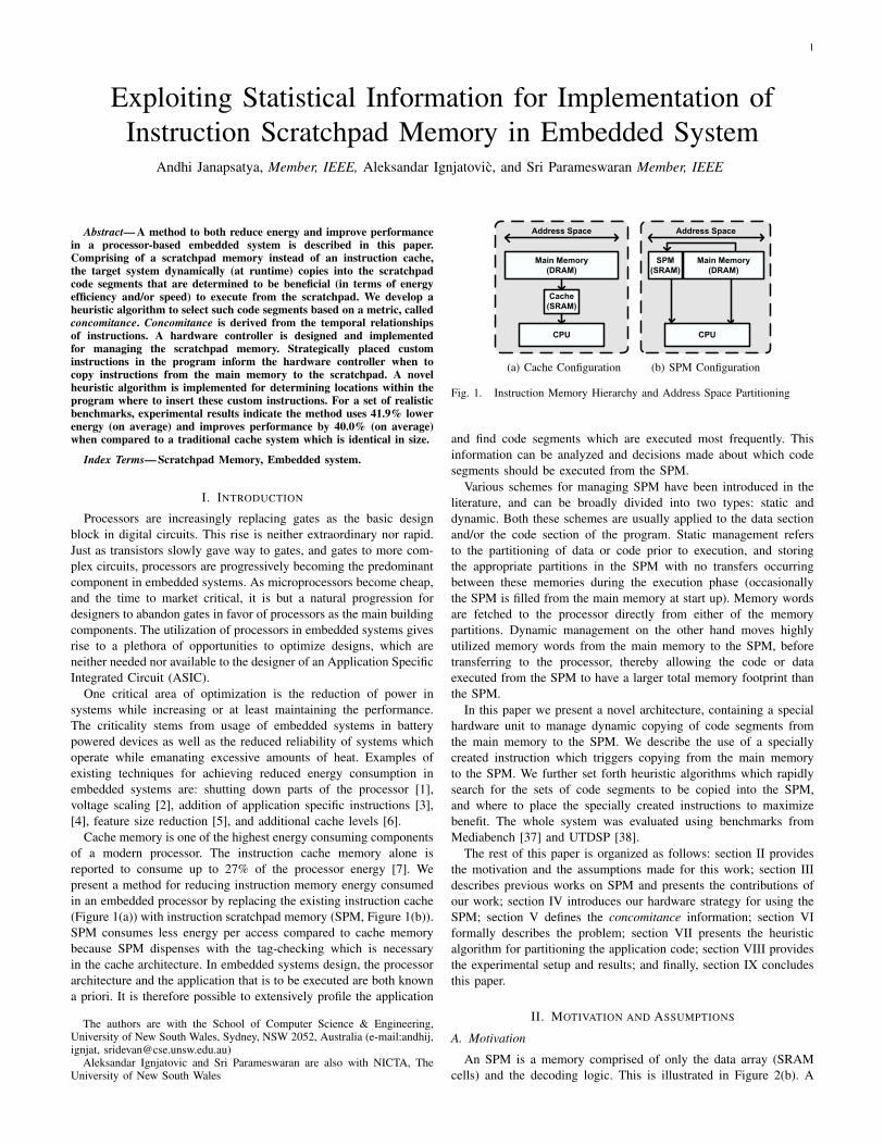
Cache memory is one of the highest energy consuming componentsof a modern processor. The instruction cache memory alone isreported to consume up to 27% of the processor energy [7]. Wepresent a method for reducing instruction memory energy consumedin an embedded processor by replacing the existing instruction cache(Figure 1(a)) with instruction scratchpad memory (SPM, Figure 1(b)).SPM consumes less energy per access compared to cache memorybecause SPM dispenses with the tag-checking which is necessaryin the cache architecture. In embedded systems design, the processorarchitecture and the application that is to be executed are both knowna priori. It is therefore possible to extensively profile the application
The authors are with the School of Computer Science & Engineering,University of New South Wales, Sydney, NSW 2052, Australia (e-mail:andhij,ignjat, [email protected])
Aleksandar Ignjatovic and Sri Parameswaran are also with NICTA, TheUniversity of New South Wales
CPU
Cache
(SRAM)
Main Memory
(DRAM)
Address Space
(a) Cache Configuration
SPM
(SRAM)
Main Memory
(DRAM)
Address Space
CPU
(b) SPM Configuration
Fig. 1. Instruction Memory Hierarchy and Address Space Partitioning
and find code segments which are executed most frequently. Thisinformation can be analyzed and decisions made about which codesegments should be executed from the SPM.
Various schemes for managing SPM have been introduced in theliterature, and can be broadly divided into two types: static anddynamic. Both these schemes are usually applied to the data sectionand/or the code section of the program. Static management refersto the partitioning of data or code prior to execution, and storingthe appropriate partitions in the SPM with no transfers occurringbetween these memories during the execution phase (occasionallythe SPM is filled from the main memory at start up). Memory wordsare fetched to the processor directly from either of the memorypartitions. Dynamic management on the other hand moves highlyutilized memory words from the main memory to the SPM, beforetransferring to the processor, thereby allowing the code or dataexecuted from the SPM to have a larger total memory footprint thanthe SPM.
In this paper we present a novel architecture, containing a specialhardware unit to manage dynamic copying of code segments fromthe main memory to the SPM. We describe the use of a speciallycreated instruction which triggers copying from the main memoryto the SPM. We further set forth heuristic algorithms which rapidlysearch for the sets of code segments to be copied into the SPM,and where to place the specially created instructions to maximizebenefit. The whole system was evaluated using benchmarks fromMediabench [37] and UTDSP [38].
The rest of this paper is organized as follows: section II providesthe motivation and the assumptions made for this work; section IIIdescribes previous works on SPM and presents the contributions ofour work; section IV introduces our hardware strategy for using theSPM; section V defines the concomitance information; section VIformally describes the problem; section VII presents the heuristicalgorithm for partitioning the application code; section VIII providesthe experimental setup and results; and finally, section IX concludesthis paper.
II. MOTIVATION AND ASSUMPTIONS
A. Motivation
An SPM is a memory comprised of only the data array (SRAMcells) and the decoding logic. This is illustrated in Figure 2(b). A
Data RAM
(SRAM)
De
cod
ing
Lo
gic
Output
Driver
tag RAM
(SRAM)
Output
Driver
Upper bits
Comparator
Logic
Memory Address
Hit/Miss Data
(a) Cache Architecture
Data RAM
(SRAM)
De
cod
ing
Lo
gic
Output
Driver
Memory Address
Data
(b) SPM Architecture
Fig. 2. Architecture of Cache in comparison to SPM.
cache shown in Figure 2(a), in comparison, has data array (SRAMcells), decoding logic, tag array (SRAM cells), and comparator logic.Comparator logic checks if the existing content in cache matches thecurrent CPU request and thus determines whether a cache hit or acache miss has occurred. The access time and the access energy ofindividual components within the cache have been estimated usingthe tool CACTI [35]. CACTI results shows that for a cache systemconsisting of 8K bytes with associativities ranging from 1 to 32, theaccess time of the cache tag-RAM array is 38.9% longer on averagecompared to access time of the cache data-RAM array and the accessenergy of the data-RAM is on average 72.5% of the total cache accessenergy.
Each piece of data is placed into the cache according to its mainmemory location, identified by the tag. Thus, cache memory istransparent to the CPU. The SPM is used as a replacement of (level 1)instruction cache. The absence of the tag array within the SPM meansthat CPU has to know where a particular instruction reside within theSPM. To allow the CPU to locate data, SPM and the DRAM span asingle memory address space, partitioned between them.
Selecting the correct code segments for placement onto the SPMrequires a careful analysis of the way such code segments areexecuted. All prior work in this area has focused upon loop analysisof the trace of a program as the method for finding the appropriatecode segments to be placed in the SPM. Loop analysis has severaldrawbacks: (i) the structure and relationship of loops can be verycomplex and thus difficult to analyse; (ii) this structure can signifi-cantly vary for different inputs; (iii) the precise structure of loops isirrelevant for the placement of instructions in the SPM because onlyrelative (temporal) proximity of executions of blocks of code matters,rather than the precise order of these instructions as provided by theloop analysis; see [9], [10], [11], [12]. Thus in this paper, insteadof looking at the loop structure, we analyze temporal correlation ofexecutions of blocks of code using statistical methods with a signalprocessing flavor. The trace is seen as a “signal” on which we performa statistical, rather than a structural analysis.
We call the measure we introduce for temporal proximity ofconsecutive executions of the same block of the code the self-concomitance of the block, and we use it to decide if the block shouldbe executed from the SPM or from the main memory. Similarly,the measure for temporal proximity of interleaved executions of twodifferent blocks of the code we call the concomitance, and use it todecide whether two blocks should be placed in SPM simultaneouslyor they can overlap in the SPM.
Such analysis of the trace has proven to yield an algorithm forSPM placement with performance results that are not only superiorto the loop analysis method, but is also much simpler, more efficient,and adaptive to different types of applications by changing only
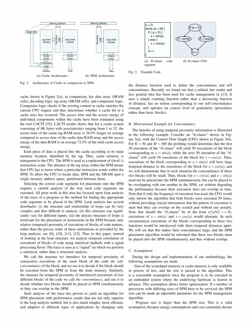
a = 0;while (a < M) { If ( a < K) { x = sin(a); } else { x = cos(a); } a++;}
(a) If-clause codesegment
X = sin(a) X = cos(a)
a++;
If (a < K)
(b) If-clause CFG
Fig. 3. Example Code
the distance function used to define the concomitance and selfconcomitance. Recently we found out that a related, but cruder andless general idea has been used for cache management in [13]. Ituses a simple counting function rather than a decreasing functionof distance, has no notion corresponding to our self-concomitanceconcept, and operates on coarser level of granularity (proceduresrather than basic blocks).
B. Motivational Example for Concomitance
The benefits of using temporal proximity information is illustratedin the following example. Consider an “if-clause” shown in Fig-ure 3(a), with the Control Flow Graph (CFG) shown in Figure 3(b).For K = 50 and M = 100 the profiling would determine that the first50 execution of the “if-clause” will yield 50 executions of the blockcorresponding to x = sin(a), while the next 50 execution of the “if-clause” will yield 50 executions of the block for x = cos(a). Thus,executions of the block corresponding to x = sin(a) will have largetemporal distance to the executions of the block for x = cos(a), andwe will demonstrate that in such situation the concomitance of thesetwo blocks will be small. Thus, blocks for x = cos(a) and x = sin(a)need not be placed into the SPM simultaneously, but can be placed tobe overlapping with one another in the SPM, yet without degradingthe performance because their execution does not overlap in time.Note that if only the frequency of execution was used, the CFG wouldonly inform the algorithm that both blocks were executed 50 times,without providing crucial information that the pattern of execution issuch that they can overlap on the scratch pad without any penalty.Note that should the “if-clause” be of the form i f (a%2 == 0),executions of x = sin(a) and x = cos(a) would alternate. In suchcircumstances executions of the blocks corresponding to these twofunctions would be interleaved with short temporal distances apart.We will see that this makes their concomitance large, and the SPMplacement algorithm would be informed that these two blocks mustbe placed into the SPM simultaneously and thus without overlap.
C. Assumptions
During the design and implementation of our methodology, thefollowing assumptions are made.
- Size of the scratchpad memory or cache memory is only availablein powers of two, and the size is passed to the algorithm. Thisis a reasonable assumption since the program is to be executed inan embedded system where the underlying hardware is known inadvance. This assumption allows better optimization. If a number ofprocessors with differing sizes of SPM have to be serviced, the SPMsize can be made an adjustable parameter for the SPM managementalgorithm.
- Program size is larger than the SPM size. This is a validassumption, because energy consumptions and cost constraints dictate

architectures with relatively small size SPM, compared to the size ofa typical application.
- Size of the largest basic block is less than or equal to the SPMsize. This assumption is quite valid in embedded systems where basicblocks are usually rather small. However, if the basic block is toolarge for the SPM, it can be split into a smaller part that fits into theSPM and the remainder that is executed from the main memory.
- Each instruction is exclusively executed from either the SPM orthe main memory. This ensures that it is never necessary to haveduplicates of parts of the code or to alter branch destinations duringthe execution of the program.
- Program traces used for profiling provide an accurate depictionof the program behavior during its execution. This assumption isreasonable when a sufficiently large input space has been applied.The amount of profiling needed to obtain a particular confidenceinterval is given in [32].
- We do not consider higher level caches. In an embedded system,where frequently there is no cache at all, it is unlikely that morethan a single level of cache is available. Moreover, having higherlevel caches would not reduce the effectiveness of the approach.
III. RELATED WORK
In the past, use of SPM replacing cache memory has been shownto improve the performance and reduce energy consumption [8].Existing works on cache optimization techniques rely on carefulplacement of instructions and/or data within the memory to ensurelow cache miss rates. Cache optimization methods generally increasethe program memory size [14], [15], [16], [17], [18], [19], [20], [21].
In 1997, Panda et al. [22] presented a scheme to statically managean SPM for use as data memory. They describe a partitioning problemfor deciding whether data variables should be located in SPM orDRAM (accessed via the data cache). Their algorithm maximizescache hit rates by allowing data variables to be executed from SPM.Avissar et al. [23] presented a different static scheme for utilizingSPM as data memory. They presented an algorithm that can partitionthe data variables as well as the data stack among different memoryunits, such as SPM , DRAM, and ROM to maximize performance.Experimental results shows that Avissar et al. were able to achieve30% performance improvement over traditional direct-mapped datacaches. By allowing part of the data stack to operate from SPM,performance improvement of 44.2% was obtained, compared to asystem without SPM.
In 2001, Kandemir et al. introduced dynamic management of SPMfor data memory [24]. Their memory architecture consisted of anSPM and a DRAM which was accessed through cache. To transferdata from DRAM into SPM, they created two new software datatransfer calls; one to read instructions from DRAM and another towrite instructions into SPM. Multiple optimization strategies werepresented to partition data variables between SPM and DRAM. Thebest results were obtained from the hand optimized version. Theirresults shows a 29.4% improvement in performance compared to atraditional cache memory system. In addition, they also show thatit is possible to obtain up to 10.2% performance improvement inusing a dynamic management scheme for SPM compared to the staticversion. The work presented in [24] applied only to well-structuredscientific and multimedia applications, with each loop nest needingindependent analysis.
In 2003, Udayakumaran and Barua [25] improved upon [24] andpresented a more general scheme for dynamic management of SPMas data memory. The method from [25] analyzes the whole programat once and aims to exploit locality throughout the whole program,instead of individual loop nesting. Reported reduction in execution
time is by an average of 31.2% over the optimal static allocationscheme.
In 2002, Steinke et al. [26] presented statically managed SPMfor both instruction and data. Their results shows on average 23%reduction in energy consumption over a cache solution.
In 2003, Angiolini et al. presented another SPM static managementscheme for data memory and instruction memory that employs apolynomial time algorithm for partitioning data and instructions intoDRAM and SPM [27]. Their results show energy improvementranging from 39% to 84% over an unpartitioned SPM. In 2004,Angiolini et al. presented a different approach to static usage schemefor SPM [28] by mapping applications to existing hardware.
In [29], Steinke et al. presented a dynamic management schemefor instruction SPM. For each instruction to be copied into theSPM, they insert a load and a store instruction. The load instructionbrings the instruction to be copied from the main memory to theprocessor, and a store instruction stores it back into SPM. Theiralgorithm for determining locations in the program for inserting loadand store instructions is based on a solution of a Integer LinearProgramming (ILP) problem that is obtained by using an ILP solver.They conducted experiments with small applications (bubble sort,heap sort, ‘biquad’ from DSP stone benchmark suit, etc.) and theirresults show on average a 29.9% energy reduction and a 25.2%performance improvement compared with a cache solution.
In 2004, Janapsatya et al. presented a hardware/software approachfor dynamic management scheme of SPM [30]. Their approachintroduces a specially designed hardware component to managethe copying of instructions from the main memory into the SPM.They utilize instructions execution frequency information to modelapplications as graph and perform graph partitioning to determinelocations within the program for initiating the copying process.
A. Contributions
Our work improves upon the state of the art in the following ways:• we design a novel architecture to perform dynamic management
of instruction code between SPM and main memory;• we replace difficult structural loop analysis of the program by
an essentially statistical method for automated decision makingregarding which basic blocks should be executed from SPM and,among them, which groups of basic blocks should be placed inthe SPM simultaneously without an overlap;
• we develop a novel graph partitioning algorithm for splitting theinstruction code into segments that will either be copied into theSPM or executed directly from the main memory, in a way thatreduces the overall energy dissipation.
We evaluated the system by using realistic embedded applicationsand show performance and energy comparisons with processors ofvarious cache sizes and differing associativities.
IV. SYSTEM ARCHITECTURE
A. Hardware Implementation
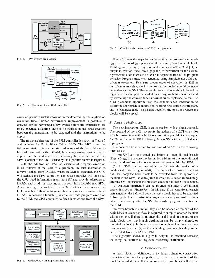
The proposed methodology modifies the processor by addingan SPM controller, which is responsible for copying instructionsfrom DRAM to SPM and stalling the CPU whenever copyingis in progress. Figure 4 shows the block diagram of the SPMcontroller, SPM, DRAM, and the CPU. A new instruction calledSMI (Scratchpad Managing Instruction) is implemented. The SMIis used to activate the SPM controller; SMIs are inserted within theprogram and are executed whenever the CPU encounters them. Thecost of the CPU stalling while the SPM is being copied is identicalto servicing a cache miss; and the number of times the SMI was
DRAMSPM
(Scratchpad
Memory)
Addr
Data
Out
Data In
Data
Out
Addr
word
select
Data
Addr
CPU
Core
stall
SPM
Controller
Instruction
OperandAddr
Read/
!Write
Fig. 4. SPM system architecture
`
Memory
Controller
sizeAddress of
SPMAddress Of
DRAM
Control
Logic
Addr
word
select
Basic Block
Table (BBT)
Special
Instruction
Operand
CPU
stall
Read/
!W rite
Fig. 5. Architecture of the SPM controller
executed provides useful information for determining the applicationexecution time. Further performance improvement is possible, ifcopying can be performed a few cycles before the instructions areto be executed assuming there is no conflict in the SPM locationbetween the instructions to be executed and the instructions to becopied.
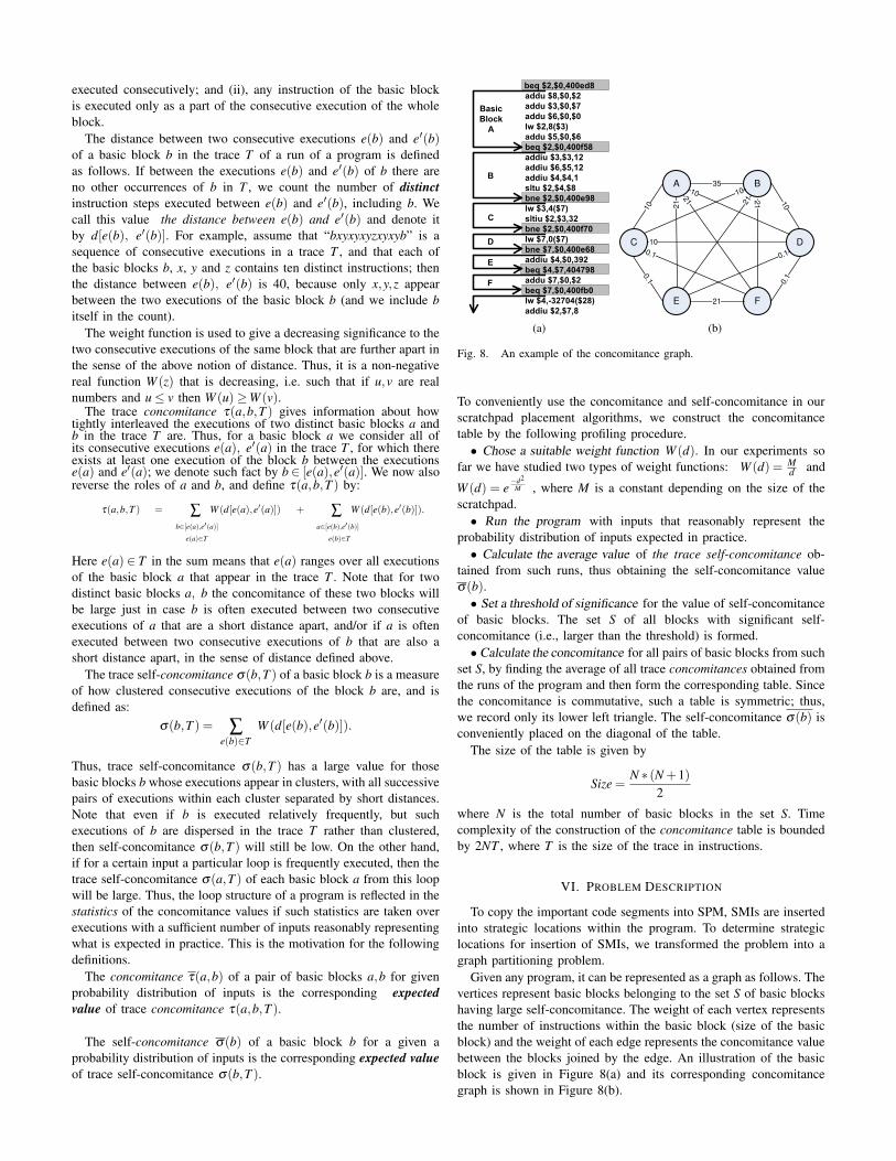
The micro-architecture of the SPM-controller is shown in Figure 5and includes the Basic Block Table (BBT). The BBT stores thefollowing static information: start addresses of the basic blocks tobe read from within the DRAM; how many instructions are to becopied; and the start addresses for storing the basic blocks into theSPM. Content of the BBT is filled by the algorithm shown in Figure 6.
With the addition of SPM, an example of program executionis as follows: at the start of a program, the first instruction isalways fetched from DRAM. When an SMI is executed, the CPUwill activate the SPM controller. The SPM controller will then stallthe CPU, read information from the BBT and provide addresses toDRAM and SPM for copying instructions from DRAM into SPM.After copying is completed, the SPM controller will release theCPU, which will then continue to fetch and execute instructions fromDRAM. Whenever a branching instruction leads program executionto the SPM, the CPU continues to fetch instructions from the SPM.
Application Profiling
C compilerAssembly/Machine
Code
Energy Model
DRAM Energy Model
SPM Controller Energy Model
SPM (SRAM) Energy Model
Simulate and Obtain
Program Trace
CPU Energy Model (Wattch)
C program Programbehavior
Graph Partitioning Algorithm
Procedure 1: Graph Partitioning
Procedure
Procedure 2: Removal of Insignificant Subgraph
Output for Implementation
Modified Assembly/
Machine code
Hardware Table Content (BBT)
Fig. 6. Methodology for Implementing the SPM
…
SMI <BBT addr>
jmp <SPM addr>
(a)
start: …
beq <dest>
…
dest: SMI <BBT addr>
jmp <SPM addr>
...
(b)
dest: …
beq <dest>
SMI <BBT addr>
jmp <SPM addr>
...
(c)
Fig. 7. Condition for insertion of SMI into programs.
Figure 6 shows the steps for implementing the proposed methodol-ogy. The methodology operates on the assembly/machine code level.Profiling and tracing (using modified simplescalar/Pisa 3.0d [31] tooutput instruction trace into a gzip file) is performed on the assem-bly/machine code to obtain an accurate representation of the programbehavior. Program trace was generated using SimpleScalar 3.0d out-of-order execution. To ensure proper order of execution of SMI inout-of-order machine, the instructions to be copied should be madedependent on the SMI. This is similar to a load operation followed byregister operation upon the loaded data. Program behavior is capturedby extracting the concomitance information as explained below. TheSPM placement algorithm uses the concomitance information todetermine appropriate locations for inserting SMI within the program,and to construct table (BBT) that specifies the positions where theblocks will be copied.
B. Software Modification
The new instruction, SMI, is an instruction with a single operand.The operand of the SMI represents the address of a BBT entry. Fora 32 bit instruction with a 16 bit operand, it is possible to have up to65536 entries in the BBT, allowing 65536 SMIs to be inserted intoa program.
The code can be modified by insertion of an SMI in the followingthree cases:
(1) An SMI can be inserted just before an unconditional branch(Figure 7(a)); in this case the destination address of the unconditionalbranch is altered to point to the correct address within the SPM.
(2) An SMI can be inserted to be the new destination of aconditional branch (Figure 7(b)); if the branch tests positive, such anSMI will copy the basic block to be executed from the appropriatelocation in the SPM; an extra jump instruction is added immediatelyafter the SMI, to transfer the program execution to that SPM location.
(3) An SMI instruction can be inserted just after a conditionalbranch instruction (Figure 7(c)). In this case, if the conditional branchtests negative, the SMI will copy the basic block that is to be executedfollowing the branch instruction. Again, an extra jump instruction isadded immediately after the SMI to transfer program execution tothe SPM.
An extra branch instruction may also be needed at the end of thebasic block if execution flow is required to jump to another locationwithin memory. If there is an unconditional branch at the end of thebasic block, then the branch destination can be simply altered, ormodified as in (1). If there are conditional branches then we mayhave to modify as per (2) or (3) depending upon whether they are tobe executed from DRAM or SPM.
The algorithm shown in Figure 6, outputs the modified softwareincluding the addition of any extra branching instructions.
V. CONCOMITANCE
A basic block, by definition, is the largest chain of consecutiveinstructions that has the properties: (i), if the first instruction of theblock is executed, then all instructions in the basic block will also be
executed consecutively; and (ii), any instruction of the basic blockis executed only as a part of the consecutive execution of the wholeblock.
The distance between two consecutive executions e(b) and e′(b)of a basic block b in the trace T of a run of a program is definedas follows. If between the executions e(b) and e′(b) of b there areno other occurrences of b in T , we count the number of distinctinstruction steps executed between e(b) and e′(b), including b. Wecall this value the distance between e(b) and e′(b) and denote itby d[e(b), e′(b)]. For example, assume that “bxyxyxyzxyxyb” is asequence of consecutive executions in a trace T , and that each ofthe basic blocks b, x, y and z contains ten distinct instructions; thenthe distance between e(b), e′(b) is 40, because only x,y,z appearbetween the two executions of the basic block b (and we include bitself in the count).
The weight function is used to give a decreasing significance to thetwo consecutive executions of the same block that are further apart inthe sense of the above notion of distance. Thus, it is a non-negativereal function W (z) that is decreasing, i.e. such that if u,v are realnumbers and u ≤ v then W (u) ≥W (v).
The trace concomitance τ(a,b,T ) gives information about howtightly interleaved the executions of two distinct basic blocks a andb in the trace T are. Thus, for a basic block a we consider all ofits consecutive executions e(a), e′(a) in the trace T , for which thereexists at least one execution of the block b between the executionse(a) and e′(a); we denote such fact by b ∈ [e(a),e′(a)]. We now alsoreverse the roles of a and b, and define τ(a,b,T ) by:
τ(a,b,T ) = ∑b∈[e(a),e′(a)]
e(a)∈T
W (d[e(a),e′(a)]) + ∑a∈[e(b),e′(b)]
e(b)∈T
W (d[e(b),e′(b)]).
Here e(a) ∈ T in the sum means that e(a) ranges over all executionsof the basic block a that appear in the trace T . Note that for twodistinct basic blocks a, b the concomitance of these two blocks willbe large just in case b is often executed between two consecutiveexecutions of a that are a short distance apart, and/or if a is oftenexecuted between two consecutive executions of b that are also ashort distance apart, in the sense of distance defined above.
The trace self-concomitance σ(b,T ) of a basic block b is a measureof how clustered consecutive executions of the block b are, and isdefined as:
σ(b,T ) = ∑e(b)∈T
W (d[e(b),e′(b)]).
Thus, trace self-concomitance σ(b,T ) has a large value for thosebasic blocks b whose executions appear in clusters, with all successivepairs of executions within each cluster separated by short distances.Note that even if b is executed relatively frequently, but suchexecutions of b are dispersed in the trace T rather than clustered,then self-concomitance σ(b,T ) will still be low. On the other hand,if for a certain input a particular loop is frequently executed, then thetrace self-concomitance σ(a,T ) of each basic block a from this loopwill be large. Thus, the loop structure of a program is reflected in thestatistics of the concomitance values if such statistics are taken overexecutions with a sufficient number of inputs reasonably representingwhat is expected in practice. This is the motivation for the followingdefinitions.
The concomitance τ(a,b) of a pair of basic blocks a,b for givenprobability distribution of inputs is the corresponding expectedvalue of trace concomitance τ(a,b,T ).
The self-concomitance σ(b) of a basic block b for a given aprobability distribution of inputs is the corresponding expected valueof trace self-concomitance σ(b,T ).
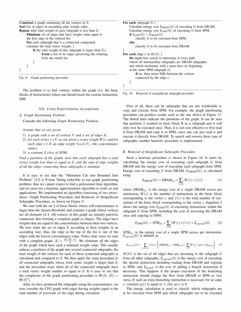
beq $2,$0,400ed8 addu $8,$0,$2 addu $3,$0,$7 addu $6,$0,$0 lw $2,8($3) addu $5,$0,$6 beq $2,$0,400f58 addiu $3,$3,12 addiu $6,$5,12 addiu $4,$4,1 sltu $2,$4,$8 bne $2,$0,400e98 lw $3,4($7) sltiu $2,$3,32 bne $2,$0,400f70 lw $7,0($7) bne $7,$0,400e68 addiu $4,$0,392 beq $4,$7,404798 addu $7,$0,$2 beq $7,$0,400fb0 lw $4,-32704($28) addiu $2,$7,8
BasicBlock
A
B
C
D
E
F
(a)
A B
E
C D
10
F
35
21
0.1
10
0.1
21
2121
10
0.1
10
0.1
21
10
(b)
Fig. 8. An example of the concomitance graph.
To conveniently use the concomitance and self-concomitance in ourscratchpad placement algorithms, we construct the concomitancetable by the following profiling procedure.• Chose a suitable weight function W (d). In our experiments so
far we have studied two types of weight functions: W (d) = Md and
W (d) = e−d2
M , where M is a constant depending on the size of thescratchpad.• Run the program with inputs that reasonably represent the
probability distribution of inputs expected in practice.• Calculate the average value of the trace self-concomitance ob-
tained from such runs, thus obtaining the self-concomitance valueσ(b).• Set a threshold of significance for the value of self-concomitance
of basic blocks. The set S of all blocks with significant self-concomitance (i.e., larger than the threshold) is formed.• Calculate the concomitance for all pairs of basic blocks from such
set S, by finding the average of all trace concomitances obtained fromthe runs of the program and then form the corresponding table. Sincethe concomitance is commutative, such a table is symmetric; thus,we record only its lower left triangle. The self-concomitance σ(b) isconveniently placed on the diagonal of the table.
The size of the table is given by
Size =N ∗ (N +1)
2
where N is the total number of basic blocks in the set S. Timecomplexity of the construction of the concomitance table is boundedby 2NT , where T is the size of the trace in instructions.
VI. PROBLEM DESCRIPTION
To copy the important code segments into SPM, SMIs are insertedinto strategic locations within the program. To determine strategiclocations for insertion of SMIs, we transformed the problem into agraph partitioning problem.
Given any program, it can be represented as a graph as follows. Thevertices represent basic blocks belonging to the set S of basic blockshaving large self-concomitance. The weight of each vertex representsthe number of instructions within the basic block (size of the basicblock) and the weight of each edge represents the concomitance valuebetween the blocks joined by the edge. An illustration of the basicblock is given in Figure 8(a) and its corresponding concomitancegraph is shown in Figure 8(b).
Construct a graph containing all the vertices in S;Sort list of edges in ascending edge weight value.Repeat until total weight of each subgraph is less than Z.
Eliminate set of edges that have weight value equal tothe first edge in the ordered list.For each subgraph that is a connected componentcalculate the total vertex weight; {
If the total weight of this subgraph is larger than Z,{Form a list of its edges preserving the orderingfrom the initial list.
}
}
}
Fig. 9. Graph partitioning procedure
The problem is to find vertices within the graph (i.e. the basicblocks of instructions) where one should insert the custom instruction,SMI.
VII. CODE PARTITIONING ALGORITHM
A. Graph Partitioning Problem
Consider the following Graph Partitioning Problem.
Assume that we are given:
1) a graph with a set of vertices V and a set of edges E;2) for each vertex v∈V we are given a vertex weight W (v) and for
each edge e ∈ E an edge weight τ(a,b,T ). (the concomitancevalue);
3) a constant Z (size of SPM)
Find a partition of the graph, such that each subgraph has a totalvertex weight less than or equal to Z, and the sum of edge weightsof all the edges connecting these subgraphs is minimal.
It is easy to see that the “Minimum Cut into Bounded SetsProblem” [33] is P-time Turing reducible to our graph partitioningproblem; thus we cannot expect to find a polynomial time algorithm,and we must use a heuristic approximation algorithm to work on realapplications. We implemented an algorithm consisting of two proce-dures: Graph Partitioning Procedure and Removal of InsignificantSubgraphs Procedure, as shown on Figure 9.
We start with the set S of basic blocks whose self-concomitance islarger than the chosen threshold, and consider a graph whose verticesare all elements of S. All vertices of this graph are initially pairwiseconnected, thus forming a complete graph (a clique). The edges haveweights that are equal to the concomitance between their two vertices.We now order the set of edges E according to their weights in anascending way; thus, the edge at the top of the list is one of theedges with the lowest concomitance value. Notice that, since we startwith a complete graph, |E| = |S|·(|S|−1)
2 . We eliminate all the edgesof the graph which have such a minimal weight value. This usuallyinduces a partition of the graph into several connected subgraphs; thetotal weight of the vertices for each of these connected subgraphs iscalculated and compared to Z. We then apply the same procedure toall connected subgraphs whose total vertex weight is larger than Z,and the procedure stops when all of the connected subgraphs havea total vertex weight smaller or equal to Z. It is easy to see thatthe complexity of the graph partitioning procedure is Θ(|S| · |E|) =Θ(|S|3).
After we have produced the subgraphs using the concomitance, wenow consider the CFG graph with edges having weights equal to thetotal number of traversals of the edge during execution.
For each subgraph G {
Calculate energy cost EDRAM(G) of executing G from DRAM,Calculate energy cost ESPM(G) of executing G from SPM,if ESPM(G) < EDRAM(G)
classify G to be executed from SPM,else
classify G to be executed from DRAM.}For each edge e in IE(G) {
Do depth-first search to determine if every pathwhose all intermediary subgraphs are DRAM subgraphs,and which terminates with e must have its beginningat the same SPM subgraph G;
if no, then insert SMI between the verticesconnected by the edge e.
}
}
Fig. 10. Removal of insignificant subgraph procedure
First of all, there can be subgraphs that are not worthwhile tocopy and execute from SPM. For example, the graph partitioningprocedure can produce results such as the one shown in Figure 11.The dotted lines indicate the partitions of the graph. It can be seenthat partition 2 resulted in basic block B as a subgraph and it willonly ever be executed once. Thus, it is not cost effective to first readit from DRAM and copy it to SPM, since one can just read it andexecute it directly from DRAM. To search and remove these type ofsubgraphs, another heuristic procedure is implemented.
B. Removal of Insignificant Subgraphs Procedure
Such a heuristic procedure is shown in Figure 10. It starts bycalculating the energy cost of executing each subgraph G fromDRAM and the energy cost of executing such subgraph from SPM.Energy cost of executing G from DRAM, EDRAM(G), is calculatedusing
EDRAM(G) = DRAMacc ∗ ∑v∈G
(W (v)∗ f (v)) (1)
where DRAMacc is the energy cost of a single DRAM access perinstruction, W (v) is the number of instructions in the basic blockcorresponding to the vertex v, and f (v) is the total number of exe-cutions of the basic block corresponding to the vertex v. Equation 2shows the energy cost ESPM(G) of executing instructions within thesubgraph G from SPM, including the cost of accessing the DRAMonce and copying to SPM.
ESPM(G) = SPMacc ∗ ∑v∈G
(W (v)∗ f (v))+Especial(G) (2)
SPMacc is the energy cost of a single SPM access per instruction.Especial(G) is defined as
Especial(G) = ∑e∈IE(G)
F(e)∗
(
(DRAMacc +SPMwrite)∗ ∑v∈G
W (v)+q(e)∗Ebranch
)
(3)
IE(G) is the set of all edges that are incoming to the subgraph Gfrom all other subgraphs; Especial(G) is the energy cost of executingthe special instruction including reading from DRAM and copyingto SPM, and Ebranch is the cost of adding a branch instruction ifnecessary. This happens if the proper execution of the branchinginstruction should change the flow from DRAM to SPM or viceversa. If such an extra branching instruction is necessary for an edgee, constant q(e) is equal to 1, else q(e) is 0.
The energy calculation is used to classify which subgraphs areto be executed from SPM and which subgraphs are to be executed

A
B
CD E F G1
11
110001000
1000
1000 1
999
1001
Subgraph 1
Subgraph 2 Subgraph 3
DRAM Subgraph
SPM Subgraph
Fig. 11. Subgraph Representation
Parameters ConfigurationIssue Queue 16 entriesLoad/Store Queue 16 entriesFetch Queue 4 entriesFetch/Decode Width 4 inst. per cycleIssue/Commit Width 4 inst. per cycleFunction Units 4 IALU, 1 IMULT, 2 FPALU, 1 FPMULTL1 ICache 8way, 2 cyclesL1 DCache 32KB, 2way, 1 cycleMemory 100 cycles for first chunk, 10 cycles the rest
TABLE ISIMPLESCALAR CONFIGURATION.
from DRAM; only subgraphs G with ESPM(G) < EDRAM(G) will beexecuted from SPM. We call such a subgraph an SPM-subgraph G.
The rest of the procedure inserts the SMI as follows. For everySPM-subgraph, it will examine all incoming edges to this subgraphIE(G). We determine if such an edge is included in a path eitherfrom another SPM-subgraph G1, or from the start of the program,and only in such cases an SMI is inserted. This means that if allpaths including this edge emanate from the same SPM-subgraph G,an SMI need not be inserted. The complexity of this procedure isΘ(|S|2), where S is the number of vertices in the graph.
For example, in the CFG shown in Figure 11, there are threesubgraphs created by the graph partitioning procedure. Subgraph 1consists of the basic block B only. Assume that the energy costestimation using equation 1 and 2 classified basic block B to beexecuted from DRAM. Consider the edge from B to D. All pathscontaining the edge from B to D also contain the edge from A to B.Since A belongs to the same SPM subgraph as D, by our procedureno SMI will be inserted in the edge from B to D. In this way weavoid unnecessary replacement of instructions that are already in theSPM.
The algorithm described in this section assumed the use of the con-comitance value for the partitioning of the graph. Similar algorithmcan be used with frequency (as in [30]) instead of concomitance, andthe results are compared in Section VIII.
VIII. EXPERIMENTAL RESULTS
A. Experimental Setup
We simulated a number of benchmarks using simplescalar/PISA3.0d [31], to obtain memory access statistics. Power figures for theCPU were calculated using Wattch [34] (for a 0.18µm process.).CACTI 3.2 [35] was used as the energy model for the cache memory.The energy model for the scratchpad memory was extracted fromCACTI as in [8]. The DRAM power figures were taken from IBMembedded DRAM SA-27E [36]. The configuration for the simulatedCPU is as shown in Table I.
All benchmarks were obtained from the Mediabench suite [37]except for the benchmark histogram which were from UTDSPtest suite [38]. The total number of instructions executed in eachbenchmark is tabulated in Table II.
0
2
4
6
8
10
12
14
16
512 1024 2048 4096 8192 16384
Cache/SPM size (Bytes)
RAMcells size (Kbits)
Cache tag-RAM
BBT-RAM
Fig. 12. Cache tag-RAM size compared to BBT size in bits.
B. Area Cost for Inclusion of SMI Hardware Controller
In cache, the tag array memory cells keep record of the entrieswithin the cache data array. While for the SPM system proposedhere, the BBT keeps a record of where each set of code segment(s)are to be placed within the SPM. Each BBT entry needs to store oneDRAM address, one SPM address, and the number of instructionsto be copied. Since the most significant bits of the SPM address isknown from the memory map (as shown in Figure 2(b)), only theleast significant bits of the SPM address need to be stored within theBBT.
For example, given DRAM size of 2M bytes, SPM size of 1Kbytes, and instruction size of 8 bytes; there exists enough space tostore up to 256K instructions within the DRAM and 128 instructionswithin the SPM. Thus, the number of instructions that need to becopied ranges from 1-128 requiring 7 bits per entry, Each DRAMaddress requires 18 bits per entry (to manage 256K instructions),and each SPM address requires 7 bits per entry. In total each BBTentry requires enough space to store 32 bits.
Figure 12 shows comparison between the number of bits in a cachetag RAM cells and the average size of the BBT for different sizecache/SPM with a main memory size of 2M bytes. The averagesize of the BBT is calculated from all the benchmarks shown inTable II. From Figure 12, it can be seen that cache tag RAMcellsgrows linearly as the cache size grows exponentially, but the BBTsize decreases as the SPM grows exponentially. BBT size decreasesas SPM size increases because with a larger SPM, fewer SMIs areneeded.
Table III showed a comparison of the total number of memoryaccesses. Performance and energy results measured from the experi-ments are shown in Table IV and Table V, and cost of adding copylocations within the program is shown in Table II.
In Table II, column 1 shows the application name, column 2gives the size of the program, column 3 the number of instructionsexecuted, column 4 gives the average number of copy locationsto be inserted (average is taken from varying SPM sizes rangingfrom 1K bytes to 16K bytes), column 5 shows the average numberof instructions that need to be copied into the SPM using theconcomitance method, column 6 and 7 present the results from usingfrequency as the edge value ([30]). Comparing figures in Table II,column 5 and column 7 shows that the number of instructions to becopied into the SPM is significantly reduced using the concomitancemethod compared to the frequency method.
An SPM controller with BBT size of 128 entries (Total size = 4096Bits) was implemented in Verilog. The SPM controller is a finite statemachine that accesses the BBT and forwards the output of the BBTas DRAM and SPM memory addresses. Power estimation of the SPMcontroller was done using a commercial power estimation tool withthe following settings: ClockFreq. = 500MHz; Voltage1.8V ; usinga 0.18µm technology. Power estimation showed that it consumed2.94mW of power. This is in comparison with cache tag power

Concomitance method Frequency methodApplication Prog. size Total no. of SMI insns Avg. no. of insn. SMI insns Avg. no. of insn.
(insn.) insn. exec. inserted copied into SPM inserted copied into SPMrawcaudio 9182 6689768 4.6 1247 30.4 741972rawdaudio 9384 12414463 4.6 1263 29.7 2704463
g721enc 11052 314594475 6.2 33751706 63 130722589g721dec 11066 302967631 4.8 12844416 58 87833725
mpeg2enc 26808 1134231679 23.4 4385032 272.86 197787388pegwitenc 20562 13483894 5.6 29795 81.6 506801pegwitdec 20562 18941701 4.2 15793 120.0 1131996pegwitkey 20562 33700290 3.2 2085 113.1 601407histogram 12620 21328862 7 2829 47 2943470
TABLE IICOST OF ADDING AND EXECUTING COPY INSTRUCTIONS.
of 159mW, obtained from CACTI [35], for a 0.18µm 64 bytes ofdirect map cache. The cache power would progressively increase forgreater ways of associativity. In addition, we also synthesized theSPM controller using Synopsys tools [39], for a 0.18µm process. Theresult shows that the SPM controller is approximately 1108 gates insize. Comparing the size of the SPM controller with a synthesizedversion of the simplescalar CPU (obtained from [40], the size of thesynthesized CPU without the cache memories is approximately 82200gates.) shows that the SPM controller is approximately 1.35% of thetotal CPU size.
C. Performance Cost to Accommodate The Execution of SMI
Table III compares the total number of memory accesses ofa cache system, the system with scratchpad using the frequencymethod for capturing the program behavior ([30]), and the systemwith scratchpad using the concomitance metric as a method forcapturing the program behavior. Column 1 in Table III gives theapplication name; column 2 shows the cache or SPM size; column3 to column 7 show the total number of cache misses for differentcache associativities; column 8 gives the total DRAM accesses usingthe frequency optimization method; column 9 shows the total DRAMaccesses obtained from using the concomitance optimization method;column 10 shows the percentage improvement of the concomitancemethod over the average values of the results of the cache system(in columns 3 to column 7); and column 11 compares the percentageimprovement of the concomitance method over the frequency method.In column 11, it is shown that the concomitance method reduces thetotal number of DRAM accesses by an average of 52.94% comparedto the frequency method. When comparison is made with a cachebased system (column 3 to 7), it is shown that the total number ofDRAM accesses for the SPM system can be larger than the totalnumber of cache misses. Despite the higher total DRAM accesses ina SPM system compared to the cache system, it does not translateto worse energy consumption and worse performance compared toa cache system (such cases are highlighted in bold in Tables III,IV, and V.) This is because the energy and time cost per SPMaccess is far less compared to the energy and time cost per cacheaccess (especially when compared to the energy and time cost ofaccessing a 16-way set associative cache.). It can also be noted thattotal number of DRAM accesses for an SPM system is comprised ofboth the number of instructions to be executed from DRAM and thetotal number of instructions copied from DRAM to SPM. Copyinginstructions from DRAM to SPM causes a sequential DRAM accesswhich consumes less power and time compared to a random DRAMaccess that happens on each cache miss.
SimpleScalarSimulation
ProgramTrace
SimpleScalar Binary
ControlFlow Graph
ConcomitanceTable
Edge CuttingProcedure based on frequency
information
Instruction Cache misses.
Time and Energy Model
Processor Model(Sim-wattch)
Cache and SPM model (CACTI)
Performance and Energy Comparison.
Edge-CutProcedure based on
concomitance informationPerformance measurement
Energy measurement
Fig. 13. Experimental Setup.
0
20
40
60
80
100
120
140
160
rawcaudio
0
50
100
150
200
250
300
rawdaudio
0
1000
20003000
4000
5000
6000
70008000
9000
10000
g721enc
0
2000
4000
6000
8000
10000
12000
g721dec
0
5000
10000
15000
20000
25000
30000
mpeg2encode
0
200
400
600
800
1000
1200
1400
pegwitenc
0
50
100
150
200
250
300
350
400
450
pegwitdec
0
50
100
150
200
250
300
350
pegwitkey
0
100
200
300
400
500
600
700
800
900
histogram
0
20
40
60
80
100
120
140
160 Assoc=1
Assoc=2
assoc=4
Assoc=8
Assoc=16
Frequency
Concomitance
Fig. 14. Energy Comparison for 8K bytes SRAM. (y-axes are energy in mJ)
D. Analysis of Results
The experimental setup for measuring the performance and energyconsumption is shown in Figure 13. Performance of the memoryarchitecture is evaluated by calculating the total memory accesses fora complete program execution. Estimation of memory access time ispossible due to known SPM access time, cache access time, DRAMaccess time, hit rates of cache and number of times the SPM contentsare changed.
Total access time of the cache architecture system is calculatedusing equation 4
cacheaccess time(ns) =(cachehit + cachemiss)∗ cachetime(ns)+
cachemiss ∗DRAMtime(ns)(4)
where cachehit is the total number of cache hits, cachemiss is thenumber of cache misses, cachetime is the access time to fetch one

SRAM Total cache misses DRAM DRAM % imp. ofsize assoc = acc. acc. conc. over
1 2 4 8 16 (freq.) (conc.) cache freq.(avg.)
rawcaudio1024 7408 6653 7818 8666 6807 3883 3004 59.4 22.62048 7052 4629 2899 2846 2852 3427 2396 32.7 30.14096 3931 4076 2334 2275 2240 3400 2092 24.1 38.58192 2154 1981 1868 1847 1830 3400 2092 -8.5 38.5
16384 2007 1841 1810 1799 1799 3400 1799 2.7 47.1rawdaudio
1024 20899 26033 29336 30530 31148 31527 12488 53.7 60.42048 14996 10389 4806 2914 2920 3470 2634 44.3 24.14096 5465 5900 2398 2352 2322 3535 2160 29.8 38.98192 2208 2035 1932 1915 1899 3535 2160 -8.5 38.9
16384 2049 1898 1878 1867 1867 3535 1867 2.2 47.2g721enc
1024 1.3E+8 1.3E+8 1.1E+8 1.1E+8 1.1E+8 1.5E+8 5.6E+7 52.6 62.82048 1.1E+8 1.1E+8 1.1E+8 1.1E+8 1.1E+8 2.1E+8 5.6E+7 47.9 73.14096 7.8E+7 8.3E+7 9.0E+7 1.0E+8 1.1E+8 3.3E+8 1.2E+8 -38.1 62.68192 5.1E+7 2.1E+7 1.4E+7 1.1E+7 4.3E+6 7.5E+5 3.0E+5 97.2 59.5
16384 3.9E+6 2.4E+6 1.1E+4 2.7E+3 2.7E+3 8.6E+3 2.7E+3 55.5 68.6g721dec
1024 1.2E+8 1.2E+8 1.1E+8 1.1E+8 1.1E+8 1.3E+8 3.0E+7 73.5 77.12048 1.0E+8 1.0E+8 1.0E+8 1.0E+8 1.0E+8 1.8E+8 3.9E+7 62.4 78.64096 7.4E+7 8.0E+7 8.5E+7 9.2E+7 1.0E+8 1.1E+8 4.1E+7 51.8 62.58192 4.1E+7 2.6E+7 8.6E+6 3.6E+6 3.7E+6 1.9E+5 4.7E+4 99.3 75.1
16384 6.6E+4 3.5E+4 1.3E+4 3.6E+3 2.8E+3 6.8E+3 2.7E+3 58.8 60.0mpeg2enc
1024 1.1E+8 1.4E+8 1.7E+8 1.8E+8 1.9E+8 2.4E+8 8.6E+7 43.6 64.22048 2.7E+7 1.1E+7 1.1E+7 1.1E+7 1.1E+7 2.5E+7 5.2E+6 58.8 79.44096 4.8E+6 4.1E+6 3.0E+6 2.8E+6 2.7E+6 6.7E+6 1.9E+6 43.4 71.98192 1.9E+6 1.0E+6 7.6E+5 7.9E+5 8.4E+5 4.5E+6 7.7E+5 19.0 82.9
16384 4.8E+5 3.7E+5 1.4E+5 1.1E+5 1.1E+5 2.8E+6 1.3E+5 21.1 95.4pegwitenc
1024 1.0E+7 9.9E+6 9.8E+6 9.8E+6 9.6E+6 9.4E+6 8.6E+6 12.4 8.62048 9.3E+6 8.7E+6 8.6E+6 8.6E+6 8.6E+6 9.0E+6 8.0E+6 8.4 10.74096 7.3E+6 8.3E+6 8.3E+6 8.4E+6 8.4E+6 9.0E+6 8.0E+6 1.6 10.78192 3.2E+6 3.5E+6 3.0E+6 3.0E+6 3.0E+6 3.4E+6 2.9E+6 6.8 13.7
16384 3.6E+5 6.4E+4 4.8E+4 6.0E+4 6.6E+4 3.6E+5 6.7E+4 4.8 81.2pegwitdec
1024 6.3E+6 6.2E+6 6.1E+6 6.2E+6 6.0E+6 5.9E+6 5.5E+6 10.8 7.42048 5.9E+6 5.6E+6 5.5E+6 5.5E+6 5.5E+6 5.7E+6 5.2E+6 6.9 8.94096 4.6E+6 5.4E+6 5.4E+6 5.4E+6 5.4E+6 5.7E+6 5.2E+6 0.1 8.98192 1.8E+5 1.9E+5 1.4E+5 1.4E+5 1.2E+5 3.7E+5 8.0E+4 46.8 78.6
16384 7.1E+4 6.3E+4 6.0E+4 7.6E+4 8.5E+4 2.5E+5 6.6E+4 6.2 73.5pegwitkey
1024 1.2E+6 1.1E+6 9.9E+5 1.0E+6 8.8E+5 7.7E+5 3.9E+5 61.8 49.82048 7.5E+5 4.4E+5 3.8E+5 3.8E+5 3.8E+5 5.3E+5 7.9E+4 81.8 85.04096 2.7E+5 2.6E+5 2.7E+5 2.9E+5 2.9E+5 5.3E+5 7.9E+4 71.2 85.08192 1.2E+5 1.3E+5 8.8E+4 8.1E+4 6.3E+4 9.7E+4 3.9E+4 56.6 59.5
16384 3.9E+4 3.1E+4 2.6E+4 3.2E+4 3.5E+4 9.7E+4 3.9E+4 -22.9 59.5histogram
1024 1.6E+7 1.7E+7 1.8E+7 1.8E+7 1.9E+7 1.9E+7 1.7E+7 5.7 14.62048 1.3E+7 1.3E+7 1.4E+7 1.4E+7 1.4E+7 1.4E+7 9.0E+6 34.1 37.44096 8.2E+6 7.1E+6 4.9E+6 3.8E+6 3.7E+6 1.4E+7 3.4E+6 32.0 74.88192 5.7E+6 1.7E+6 2.6E+5 1.5E+4 3.5E+3 7.8E+4 9.2E+3 34.6 88.2
16384 4.2E+6 4.5E+5 3.3E+3 3.0E+3 2.9E+3 8.5E+3 2.8E+3 44.0 66.3
TABLE IIITOTAL MEMORY ACCESS COMPARISON.(CACHE RESULT SHOWS THE
TOTAL CACHE MISSES. DRAM ACCESS IS THE TOTAL NUMBER OF
INSTRUCTIONS EXECUTED FROM DRAM PLUS THE NUMBER OF
INSTRUCTIONS COPIED FROM DRAM TO THE SPM.)
instruction from the cache, and DRAMtime is the amount of timespent to access one DRAM instruction.We estimate the total memory access time for the SPM architectureusing equation 5,
SPMaccess time(ns) =SPMexe ∗SPMtime(ns)+
SMIexe ∗ copysize ∗DRAMtime(ns)+
DRAMexe ∗DRAMtime(ns)(5)
where SPMexe is the number of instructions executed from SPM,SPMtime is the amount of time needed to fetch one instruction fromthe SPM, SMIexe is the total number of times all SMIs are executed,copysize is the total number of instructions copied from DRAM
SRAM Cache System’s Energy (mJ) SPM SPM % imp. ofsize assoc = (mJ) (mJ) conc. over
1 2 4 8 16 (freq.) (conc.) cache freq.(avg.)
rawcaudio1024 101 105 105 113 130 69 59 45.9 13.62048 103 106 106 117 132 73 64 43.2 12.64096 109 111 111 118 138 77 66 43.2 14.38192 116 118 118 122 140 92 70 42.5 23.3
16384 140 139 139 147 165 99 75 48.5 24.2rawdaudio
1024 194 201 201 217 249 157 116 45.1 26.12048 197 200 200 222 249 161 122 42.4 24.24096 207 211 211 223 260 170 127 42.3 25.08192 219 223 223 230 264 196 135 41.7 31.4
16384 265 263 263 277 310 210 143 47.7 31.6g721enc
1024 25763 23507 23507 23753 24470 18397 10082 58.3 45.22048 22782 22856 22856 23473 24123 22071 8920 61.6 59.64096 18919 20190 20190 22273 24056 32151 14548 30.6 54.88192 8880 7906 7906 7595 7314 4557 3356 57.5 26.4
16384 7016 6568 6568 6932 7778 4832 3552 48.9 26.5g721dec
1024 24830 22514 22514 22552 23315 16092 7185 68.9 55.42048 21745 22026 22026 22589 23340 19071 6843 69.4 64.14096 18141 19137 19137 20672 22841 13214 6968 64.9 47.38192 9562 6779 6779 6104 6969 4357 3215 54.5 26.2
16384 6382 6327 6327 6677 7493 4664 3422 48.3 26.6mpeg2enc
1024 39931 44684 44684 49043 52774 34447 22183 51.6 35.62048 19399 19849 19849 21853 24341 14118 11612 44.5 17.84096 19292 19502 19502 20636 23970 13218 11636 43.1 12.08192 19971 20294 20294 20941 24068 15421 12174 42.1 21.1
16384 24032 23793 23793 25099 28151 16479 12907 48.1 21.7pegwitenc
1024 2161 2141 2141 2200 2242 1780 1621 25.5 8.92048 1964 1949 1949 2014 2082 1712 1543 22.5 9.94096 1929 1947 1947 1977 2088 1730 1554 21.4 10.28192 1157 1105 1105 1116 1192 970 795 29.9 18.0
16384 717 711 711 752 838 553 381 48.7 31.1pegwitdec
1024 1312 1310 1310 1337 1365 1106 1016 23.4 8.12048 1215 1211 1211 1244 1286 1071 978 20.7 8.74096 1201 1208 1208 1231 1288 1081 984 19.8 9.08192 361 361 361 370 419 313 213 42.9 31.9
16384 411 407 407 431 483 322 224 47.3 30.3pegwitkey
1024 379 374 374 394 407 240 180 53.2 24.92048 282 276 276 300 330 205 141 51.6 31.24096 264 269 269 287 328 215 147 47.8 31.68192 256 254 254 260 294 205 149 43.4 27.4
16384 289 286 286 303 340 219 158 47.2 27.8histogram
1024 3468 3585 3585 3656 3793 3061 2740 24.2 10.52048 3050 3122 3122 3120 3176 2094 1580 49.3 24.54096 1921 1708 1708 1591 1442 1624 735 55.7 54.88192 830 474 474 441 507 322 229 55.8 29.0
16384 607 504 504 532 596 339 243 55.4 28.3
TABLE IVSYSTEM’S ENERGY COMPARISON.
to SPM during program runtime, and DRAMexe is the number ofinstruction executed from DRAM.SPM memory access time is compared to cache memory access timeusing the following equation.
%improvement =
100−((SPMaccess time(ns)/cacheaccess time(ns))∗100)(6)
Energy consumption comparison is shown in Table IV. The cacheenergy consumption is calculated using equation 7,
cacheenergy =(cachehit + cachemiss)∗Ecache+
cachemiss ∗EDRAM + cacheaccess time ∗ECPU(7)
where EDRAM is the energy cost per DRAM access and ECPU is theenergy consumed by the CPU.
SRAM Cache System Execution Time (ms) SPM SPM % imp. ofsize assoc = (ms) (ms) conc. over
1 2 4 8 16 (freq.) (conc.) cache freq.(avg.)
rawcaudio1024 7.9 8.0 8.0 8.4 9.1 5.2 4.7 43.3 10.82048 8.1 8.1 8.1 8.7 9.2 5.6 5.0 40.5 9.94096 8.5 8.5 8.5 8.8 9.7 5.9 5.2 40.5 11.88192 9.0 9.0 9.0 9.0 9.9 7.0 5.5 39.7 21.3
16384 11.0 10.7 10.7 11.0 11.8 7.6 5.9 46.4 22.1rawdaudio
1024 14.8 15.1 15.1 15.7 17.1 9.9 8.8 43.5 11.72048 15.0 15.0 15.0 16.1 17.1 10.3 9.3 40.6 9.84096 15.8 15.8 15.8 16.2 18.0 11.0 9.7 40.5 11.78192 16.7 16.8 16.8 16.7 18.3 13.0 10.3 39.7 21.3
16384 20.3 19.8 19.8 20.4 21.9 14.0 10.9 46.4 22.1g721enc
1024 2016.8 1832.5 1832.5 1837.3 1864.5 1443.5 798.4 57.4 44.72048 1782.8 1781.3 1781.3 1815.6 1837.2 1747.1 703.8 60.9 59.74096 1479.5 1571.8 1571.8 1720.7 1831.8 2563.4 1147.7 29.4 55.28192 690.9 607.3 607.3 567.7 517.3 335.0 261.8 55.8 21.9
16384 545.1 502.2 502.2 516.9 554.1 355.4 277.1 47.0 22.0g721dec
1024 1943.6 1754.9 1754.9 1744.0 1775.8 1260.1 568.2 68.3 54.92048 1701.5 1716.5 1716.5 1747.1 1777.6 1507.9 538.6 68.9 64.34096 1418.5 1489.5 1489.5 1596.0 1738.3 1034.2 548.0 64.4 47.08192 744.5 519.2 519.2 451.5 492.2 319.1 250.6 52.7 21.5
16384 495.5 483.6 483.6 497.8 533.6 342.2 266.8 46.4 22.0mpeg2enc
1024 3142.5 3495.2 3495.2 3789.4 3978.2 2762.6 1742.9 51.0 36.92048 1500.8 1509.6 1509.6 1616.0 1705.0 1123.1 899.1 42.5 19.94096 1490.0 1479.5 1479.5 1516.2 1673.6 1048.2 900.3 40.9 14.18192 1539.2 1538.7 1538.7 1534.4 1678.0 1221.2 942.9 39.7 22.8
16384 1859.7 1812.6 1812.6 1865.2 1999.5 1300.3 1000.2 46.4 23.1pegwitenc
1024 169.0 166.6 166.6 169.7 169.9 136.6 128.8 23.5 5.72048 153.5 151.5 151.5 155.1 157.3 131.4 122.6 20.3 6.74096 150.7 151.3 151.3 152.2 157.8 132.8 123.4 19.1 7.18192 90.1 85.2 85.2 84.4 87.4 73.1 62.8 27.3 14.1
16384 55.6 54.3 54.3 56.0 59.7 40.3 29.6 47.0 26.5pegwitdec
1024 102.6 102.0 102.0 103.3 103.7 84.9 80.8 21.3 4.82048 95.0 94.2 94.2 95.9 97.5 82.2 77.7 18.5 5.44096 93.8 93.9 93.9 94.9 97.6 83.0 78.2 17.5 5.88192 27.9 27.4 27.4 27.2 29.4 22.7 16.5 40.6 27.1
16384 31.8 31.0 31.0 32.1 34.4 23.3 17.4 45.6 25.3pegwitkey
1024 29.5 28.8 28.8 29.7 29.6 17.8 14.1 51.8 20.62048 21.9 21.1 21.1 22.4 23.5 15.1 11.0 50.0 27.14096 20.5 20.6 20.6 21.3 23.3 15.8 11.4 46.0 27.68192 19.8 19.3 19.3 19.2 20.6 15.0 11.6 41.0 22.6
16384 22.4 21.9 21.9 22.6 24.2 16.1 12.3 45.3 23.2histogram
1024 271.6 280.3 280.3 284.8 293.3 238.3 218.5 22.5 8.32048 238.9 244.0 244.0 242.7 244.9 162.9 125.8 48.2 22.84096 150.2 132.9 132.9 122.7 108.8 127.0 58.2 54.6 54.28192 64.6 36.1 36.1 32.4 35.4 22.9 17.7 54.0 22.8
16384 47.1 38.4 38.4 39.5 42.4 24.1 18.8 54.0 22.1
TABLE VSYSTEM’S PERFORMANCE COMPARISON.
The SPM energy is calculated using equation 8,
SPMenergy =ESPM ∗SPMexe +EDRAM ∗DRAMexe+
K ∗ESMI + J ∗Ebranch +SPMaccess time ∗ECPU(8)
where ESPM is the energy cost per SPM access, ESMI is the energycost per execution of the special instruction, K is the total number oftimes SMIs are executed, Ebranch is the energy cost for any additionalbranch instructions, and J is the total number of times any additionalbranch instructions are executed.The percentage difference between the SPM energy consumptionand the cache energy consumption is calculated using the followingequation.
%energy improvement = 100− ((SPMenergy/avg cacheenergy)∗100) (9)
Results of the percentage energy improvement is shown in Table IV.
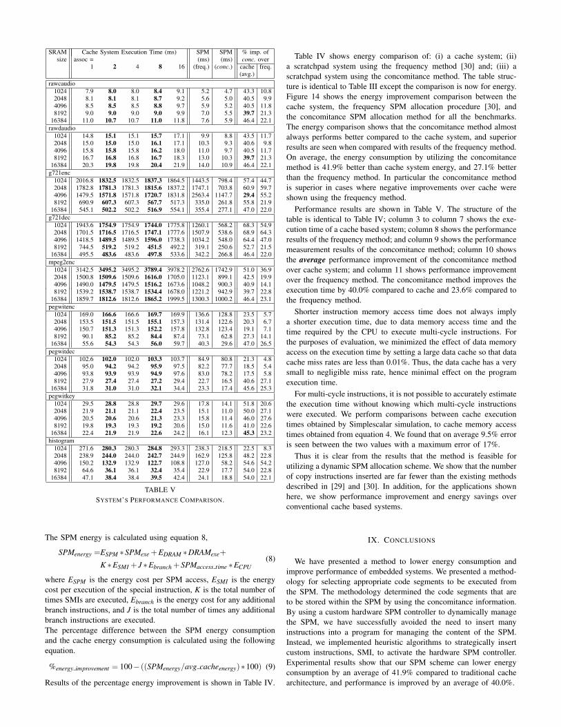
Table IV shows energy comparison of: (i) a cache system; (ii)a scratchpad system using the frequency method [30] and; (iii) ascratchpad system using the concomitance method. The table struc-ture is identical to Table III except the comparison is now for energy.Figure 14 shows the energy improvement comparison between thecache system, the frequency SPM allocation procedure [30], andthe concomitance SPM allocation method for all the benchmarks.The energy comparison shows that the concomitance method almostalways performs better compared to the cache system, and superiorresults are seen when compared with results of the frequency method.On average, the energy consumption by utilizing the concomitancemethod is 41.9% better than cache system energy, and 27.1% betterthan the frequency method. In particular the concomitance methodis superior in cases where negative improvements over cache wereshown using the frequency method.
Performance results are shown in Table V. The structure of thetable is identical to Table IV; column 3 to column 7 shows the exe-cution time of a cache based system; column 8 shows the performanceresults of the frequency method; and column 9 shows the performancemeasurement results of the concomitance method; column 10 showsthe average performance improvement of the concomitance methodover cache system; and column 11 shows performance improvementover the frequency method. The concomitance method improves theexecution time by 40.0% compared to cache and 23.6% compared tothe frequency method.
Shorter instruction memory access time does not always implya shorter execution time, due to data memory access time and thetime required by the CPU to execute multi-cycle instructions. Forthe purposes of evaluation, we minimized the effect of data memoryaccess on the execution time by setting a large data cache so that datacache miss rates are less than 0.01%. Thus, the data cache has a verysmall to negligible miss rate, hence minimal effect on the programexecution time.
For multi-cycle instructions, it is not possible to accurately estimatethe execution time without knowing which multi-cycle instructionswere executed. We perform comparisons between cache executiontimes obtained by Simplescalar simulation, to cache memory accesstimes obtained from equation 4. We found that on average 9.5% erroris seen between the two values with a maximum error of 17%.
Thus it is clear from the results that the method is feasible forutilizing a dynamic SPM allocation scheme. We show that the numberof copy instructions inserted are far fewer than the existing methodsdescribed in [29] and [30]. In addition, for the applications shownhere, we show performance improvement and energy savings overconventional cache based systems.
IX. CONCLUSIONS
We have presented a method to lower energy consumption andimprove performance of embedded systems. We presented a method-ology for selecting appropriate code segments to be executed fromthe SPM. The methodology determined the code segments that areto be stored within the SPM by using the concomitance information.By using a custom hardware SPM controller to dynamically managethe SPM, we have successfully avoided the need to insert manyinstructions into a program for managing the content of the SPM.Instead, we implemented heuristic algorithms to strategically insertcustom instructions, SMI, to activate the hardware SPM controller.Experimental results show that our SPM scheme can lower energyconsumption by an average of 41.9% compared to traditional cachearchitecture, and performance is improved by an average of 40.0%.

REFERENCES
[1] K. Lahiri, S. Dey, and A. Raghunathan, “Communication ArchitectureBased Power Management for Battery Efficient System Design,” DesignAutomation Conference. 39th Annual Proceedings of, 2002.
[2] J. Luo and N. K. Jha, “Power-profile Driven Variable Voltage Scaling forHeterogeneous Distributed Real-time Embedded Systems,” VLSI Design.Proceedings of, 2003.
[3] F. Sun, S. Ravi, A. Raghunathan, and N. K. Jha, “Custom-InstructionSynthesis for Extensible-Processor Platforms,” Computer Aided Design.IEEE Transactions on, vol.23, no.2, pp.216-228, 2004.
[4] N. Cheung, S. Parameswaran, and J. Henkel, “A quantitative study andestimation models for extensible instructions in embedded processors,”International Conference on Computer Aided Design. Proceedings of,2004.
[5] J. M. Rabaey, “Digital Integrated Circuits: A Design Perspective,”Prentice Hall, 1996.
[6] J. Kin, G. Munish, and W. H. Mangione-Smith, “The Filter Cache:An Energy Efficient Memory Structure,” Microarchitecture. 30th AnnualIEEE conference on, 1997.
[7] J. Montanaro et al., “A 160MHz, 32b, 0.5W CMOS RISC microproces-sor,” Solid State Circuit. IEEE Journal of, vol.31, no.11, pp. 1703-1714,1996.
[8] R. Banakar et al., “Scratchpad Memory: A Design Alternative forCache On-chip Memory in Embedded Systems,” Conference on Hard-ware/Software Codesign. Proceedings of, 2002.
[9] G. Ramalingam, “On Loops, Dominators, and Dominance Frontier,”Programming Language Design and Implementation. Conference on,pp.233-241, 2000.
[10] P. Havlak, “Nesting of Reducible and Irreducible Loops,” ProgrammingLanguages and Systems. ACM Transactions on, vol.19, no.4, 1997.
[11] V. C. Sreedhar, G. R. Gao, and Y. F. Lee, “Identifying Loops using DJGraphs,” Programming Languages and Systems. ACM Transactions on,vol.18, no.6, 1996.
[12] B. Steensgaard, “Sequentializing Program Dependence Graphs for Ir-reducible Programs,” Technical Report MSR TR-93-14, Microsoft Re-search, Redmond, Washington, October 1993.
[13] N. Gloy and M. D. Smith, “Procedure Placement Using Temporal-Ordering Information,” Programming Languages and Systems. ACMTransactions on, Vol. 32, No. 5, Pages 977-1027, September 1999.
[14] S. Parameswaran and J. Henkel, “I-CoPES: fast instruction code place-ment for embedded systems to improve performance and energy effi-ciency,” International Conference on Computer Aided Design. Proceed-ings of, 2001.
[15] P. P. Chang and et al., “IMPACT: an architectural framework formultiple-instruction-issue processors,” Computer Architecture News, vol.19, no. 3, 1991.
[16] S. McFarling, “Program optimization for instruction caches,” Archi-tectural Support for Programming Language and Operating Systems.Proceedings of the 3rd, 1989.
[17] S. McFarling, “Procedure merging with instruction caches,” SIGPLANNotices, vol. 26, no. 6, 1991.
[18] P. R. Panda, N. D. Dutt, and A. Nicolau, “Memory Organization for Im-proved Data Cache Performance in Embedded Processors, InternationalSymposium on System Synthesis. Proceedings of the 9th,, 1996.
[19] P. R. Panda, H. Nakamura, N. D. Dutt, and A. Nicolau, “A DataAlignment Technique for Improving Cache Performance,” InternationalConference on Computer Design. Proceedings of,, 1997.
[20] H. Tomiyama and H. Yasuura, “Optimal code Placement of EmbeddedSoftware for Instruction Cache,” The European Conference EuropeanExhibition on Design Automation Test Conference, 1996.
[21] S. Bartolini and C. A. Prete, “A cache-aware program transformationtechnique suitable for embedded systems,” Information and SoftwareTechnology, vol.44, no.13, 2002.
[22] P. R. Panda, N. D. Dutt, and A. Nicolau, “Efficient Utilization of Scratch-Pad Memory in Embedded Processor Applications,” European Designand Test Conference, Proceedings of, 1997.
[23] O. Avissar and R Barua, “An Optimal Memory Allocation Scheme forScratch-Pad-Based Embedded Systems,” ACM Transactions on Embed-ded Computing Systems, vol. 1, pp. 6-26, 2002.
[24] M. Kandemir and A. Choudhary, “Compiler-Directed Scratch Pad Mem-ory Hierarchy Design and Management,” Design Automation Confer-ence. Proceedings of 39th, 2002.
[25] S. Udayakumaran and R. Barua, “Compiler-Decided Dynamic MemoryAllocation for Scratch-Pac Based Embedded Systems,” InternationalConference on Compilers, Architecture, and Synthesis for EmbeddedSystems. Proceedings of the, 2003.
[26] S. Steinke, L. Wehmeyer, B. Lee, and P. Marwedel, “Assigning Programand Data Objects to Scratchpad for Energy Reduction,” Conference onDesign, Automation, and Test in Europe. Proceedings of the, 2002.
[27] F. Angiolini, L. Benini, and A. Caprara, “Polynomial-Time Algorithmfor On-Chip Scratchpad Memory Partitioning,” International Conferenceon Compilers, Architecture, and Synthesis for Embedded Systems. Pro-ceedings of the, 2003.
[28] F. Angiolini et al., “A Post-Compiler Approach to Scratchpad Mappingof Code,” International Conference on Compilers, Architecture, andSynthesis for Embedded Systems. Proceedings of the, 2004.
[29] S. Steinke et al., “Reducing Energy Consumption by Dynamic Copyingof Instructions onto Onchip Memory,” International Symposium onSystem Synthesis. Proceedings of the 15th, 2002.
[30] A. Janapsatya, A. Ignjatovic, and S. Parameswaran, “Hardware/SoftwareManaged Scratchpad Memory for Embedded System”, InternationalConference on Computer Aided Design. Proceedings of, 2004.
[31] D. Burger and T. M. Austin, “The SimpleScalar Tool Set, Version 2.0,”TR-CS-1342 (http://www.simplescalar.com), University of Wisconsin-madison, June 1997.
[32] P. Bartlett et al., “Profiling in the ASP Codesign Environment,” Journalof Systems Architecture, vol. 46, no. 14, pp. 1263-1274, Elsevier,Netherlands, Dec. 2000.
[33] M. R. Garey and D. S. Johnson, “Computers and Intractability,” W. H.Freeman and Company, New York, 2000.
[34] D. Brooks, V. Tiwari, and M. Martonosi, “Wattch: A Framework forArchitectural-Level Power Analysis and Optimizations,” InternationalSymposium on Computer Architecture. Proceedings of the 27th, 2000.
[35] P. Shivakumar and N. P. Jouppi, “Cacti 3.0: An Integrated Cache Timing,Power, and Area Model,” Technical Report 2001/2, Compaq ComputerCorporation, August, 2001. 2001.
[36] IBM Microelectronics Division, “Embedded DRAM SA-27E,”http://ibm.com/chips, 2002.
[37] C. Lee et al., “MediaBench: A Tool for Evaluating Multimedia and Com-munications Systems,” Microarchitecture. 30th Annual IEEE conferenceon, 1997.
[38] C. Lee and M. Stoodley, “UTDSP Benchmark Suite,” http://www.eecg.toronto.edu/ corinna/DSP/infrastructure/UTDSP.html, 1992.
[39] Synopsys Inc., “Synopsys - Electronic Design Automation Solutions andServices,” http://www.synopsys.com, 2005.
[40] J. Peddersen, S. L. Shee, A. Janapsatya, and S. Parameswaran, “RapidEmbedded Hardware/Software System Generation,” International Con-ference on VLSI Design. Proceedings of the 18th, 2005.
Andhi Janapsatya (S’00-M’06) received his B.E.(Honors) degree in electrical engineering from TheUniversity of Queensland in Brisbane, Australia, in2001. He is currently pursuing his Ph.D. at TheUniversity of New South Wales in Sydney, Australia(submitted Oct 2005). His research interest includelow power design, application specific hardwaredesign, and energy and performance optimization ofapplication specific systems.
Aleksandar Ignjatovic̀ received Bachelor’s andMaster’s degrees in Mathematics at the University ofBelgrade, former Yugoslavia, and in 1990 Ph.D. inMathematical Logic at the University of Californiaat Berkeley. He was an Assistant Professor of Math-ematical Logic and Philosophy at the Carnegie Mel-lon University before starting Kromos TechnologyInc. Presently he is a senior lecturer at the School ofComputer Science and Engineering at the Universityof New South Wales in Sydney. His interests includeapplications of Mathematical Logic to Complexity
Theory, Approximation Theory, Algorithms and Embedded Systems Design.
Sri Parameswaran is an Associate Professor in theSchool of Computer Science and Engineering. Healso serves as the Program Director for ComputerEngineering at the University of New South Wales.Sri has received the Faculty of Engineering Teach-ing Staff Excellence Award in 2005. His researchinterests are in System Level Synthesis, Low powersystems, High Level Systems and Network on Chips.He has served on the Program Committees of numer-ous International Conferences, such as Design andTest in Europe (DATE), the International Conference
on Computer Aided Design (ICCAD), the International Conference on Hard-ware/Software Codesign and System Synthesis (CODES-ISSS), Asia SouthPacific Design Automation Conference (ASP-DAC) and the InternationalConference on Compilers, Architectures and Synthesis for Embedded Systems(CASES). He has received best paper nominations from the InternationalConference on VLSI Design and the Asia South Pacific Design AutomationConference.


![IEEE TRANSACTIONS ON VERY LARGE SCALE …ece.gmu.edu/~hhomayou/files/TVLSI-peripherals.pdf · 1Results were obtained for TSMC, TOSHIBA, IBM, UMC and CHAR- ... [22] for65nmtechnology](https://img.pdfslide.net/doc/110x75/5b04338f7f8b9a2e228d7822/ieee-transactions-on-very-large-scale-ecegmueduhhomayoufilestvlsi-were.jpg)