Embed Size (px)
Citation preview
Exploring the Design Space of Power-Aware Opto-Electronic Networked SystemsXuning Chen† Li-Shiuan Peh† Gu-Yeon Wei‡ Yue-Kai Huang† Paul Prucnal†
†Dept. of Electrical Engineering, Princeton University,Princeton, NJ 08544
‡Dept. of Electrical Engineering & Computer Science,Harvard University, Cambridge, MA 02138
Abstract
As microprocessors become increasingly intercon-nected, the power consumed by the interconnection networkcan no longer be ignored. Moreover, with demand for linkbandwidth increasing, optical links are replacing electricallinks in inter-chassis and inter-board environments. As a re-sult, the power dissipation of optical links is becoming ascritical as their speed. In this paper, we first explore op-tions for building high speed opto-electronic links and discussthe power characteristics of different link components. Then,we propose circuit and network mechanisms that can realizepower-aware optical links – links whose power consumptioncan be tuned dynamically in response to changes in networktraffic. Finally, we incorporate power-control policies alongwith the power characterization of link circuitry into a de-tailed network simulator to evaluate the performance cost andpower savings of building power-aware opto-electronic net-worked systems. Simulation results show that more than 75%savings in power consumption can be achieved with the pro-posed power-aware opto-electronic network.
1 Introduction
Computer systems are increasingly composed ofsubsystems connected with an interconnection network fabric– such as clusters of PCs, servers composed of compute and/orstorage blades, supercomputers built from boxes and boards ofmicroprocessors. Due to tight cooling budgets, power is be-coming the key constraint limiting scalability in these systems.With link circuitry consuming a significant portion of the sys-tem power budget (60% of the line card power budget in theAvici TSR router [4], and 70% of the switch power budget inthe IBM InfiniBand 8-port 12X switch [6]), there is a clear in-centive to focus on improving the power efficiency for this partof the system.
As bandwidth demands increase, opto-electroniclinks are becoming the de-facto interconnect between boxes,and moving into the board-to-board domain as well. While anoptical link enables high bit rates, it does not ease the powerconsumption problem, prompting companies and researchersto find ways to reduce power in optical links [22]. In this pa-per, we investigate a power-aware architecture that uses power-control policies to dynamically control the bit rate and powerconsumption of opto-electronic links.
Power-aware networks that regulate their powerconsumption in response to actual traffic utilization were firstproposed in [24], which explored the use of dynamic voltagescalable (DVS) electrical links in networks, with routers con-trolling and setting the link bit rates. Since then, there havebeen various studies on power-aware networks – exploring theimpact of DVS on on-chip interconnects’ transmission energy
and bit error rate [30], exploring power-aware networks whereelectrical links are turned completely on and off [26], inves-tigating the control of DVS links in clusters of workstationsthrough routing table reconfiguration [11]. These prior worksfocused on network design, exploring different policies for thecontrolling of the power-aware network, glossing over the cir-cuit design issues of a power-aware link, and its impact on thecontrol policy and the overall network architecture.
The motivation to explore the possibility of design-ing power-aware opto-electronic network systems is two fold.First, as with electrical links, opto-electronic links consumesignificant power, and have a power profile that does not varysignificantly with actual utilization, so the interconnection fab-ric in these systems can consume high power even when thesystem is lightly-loaded. Second, since real-life network traf-fic exhibits substantial temporal and spatial variance [14, 26],opto-electronic networks that can regulate their own powerconsumption at run-time by tuning their bit-rate and supplyvoltage with respect to network traffic stand to gain significantpower savings.
In this paper, we explore the design space of power-aware opto-electronic networks from the bottom up, first in-vestigating ways to incorporate run-time power-control intoeach component of a link, understanding the limits, then de-signing and architecting a complete power-aware networkedsystem with routers that dynamically control the power con-sumed by the opto-electronic links. Section 2 dives into thevarious components of an opto-electronic link to show howeach works, their power characteristics, and ways to incorpo-rate power-control into each component. Section 3 presents acomplete power-aware opto-electronic network design, whichdiffers from traditional network design in both topology aswell as router microarchitecture. To evaluate this design, net-work simulations are run using both synthetic and actual traffictraces. The simulation setup and results are shown in Section 4.Section 5 concludes the paper and discusses our next steps inprototyping the proposed system. This paper is the result of acollaborative effort between optics, electronics, and networksresearchers to make power-aware opto-electronic networks areality.
2 Power-aware opto-electronic link design
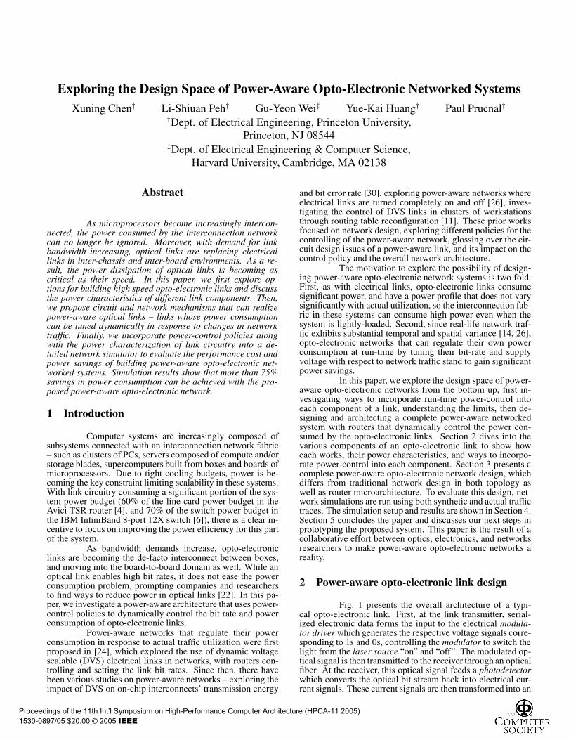
Fig. 1 presents the overall architecture of a typi-cal opto-electronic link. First, at the link transmitter, serial-ized electronic data forms the input to the electrical modula-tor driver which generates the respective voltage signals corre-sponding to 1s and 0s, controlling the modulator to switch thelight from the laser source “on” and “off”. The modulated op-tical signal is then transmitted to the receiver through an opticalfiber. At the receiver, this optical signal feeds a photodetectorwhich converts the optical bit stream back into electrical cur-rent signals. These current signals are then transformed into an
Proceedings of the 11th Int’l Symposium on High-Performance Computer Architecture (HPCA-11 2005)
1530-0897/05 $20.00 © 2005 IEEE
amplified voltage signal via a transimpedance amplifier (TIA).Finally, the clock and data recovery (CDR) circuit tracks theamplified voltage signal and extracts the digital 1s and 0s.
In the subsequent subsections, we outline designconsiderations for applying dynamic power control mecha-nisms to an opto-electronic link. For each link component,we first explain how it works, characterize what affects itspower dissipation, then propose ways to incorporate dynamicpower-control for a power-aware network system. Our pro-posals for incorporating power-control into opto-electroniclinks build upon prior research of variable-frequency electroniclinks [28, 12]. Essentially, there are two ways of realizingpower-awareness – controlling just the link bit rate, or con-trolling both bit rate and supply voltage, with respect to thenetwork traffic. We’ll discuss the implications of these alter-natives for every link component.
2.1 Transmitter: Laser source and modulator
There are two basic alternatives for implementingthe light source opto-electronic links used in board-to-boardand box-to-box networks: (1) Vertical cavity surface emittinglasers (VCSELs), where light is generated on chip and directlymodulated by electrical drive currents; (2) An external lasersource housed in a separate chassis, feeding the hundreds tothousands of transmitters within the system, with multiple-quantum-well (MQW) modulators [16] that switch light “on”and “off” based on electrically driven signals.
2.1.1 Transmitter: Directly modulated VCSELs &driver
Operation. VCSELs are controlled electronically – when theinput driving current is above a certain threshold (Ith) the VC-SEL is stimulated and it emits light. At high bit rates, thisthreshold not only affects light generation, but also the timerequired for the stimulated emission to stabilize [16]. There-fore, a VCSEL is usually constantly biased at a current abovethis threshold (Ibias). The VCSEL driver modulates the driv-ing current to the VCSEL based on the input bit patterns, sothat the driving current, I , is Im + Ibias (Im is the modulationcurrent) for bit 1, and just Ibias for bit 0. The VCSEL thenconverts 1s and 0s into high and low light intensities, respec-tively.
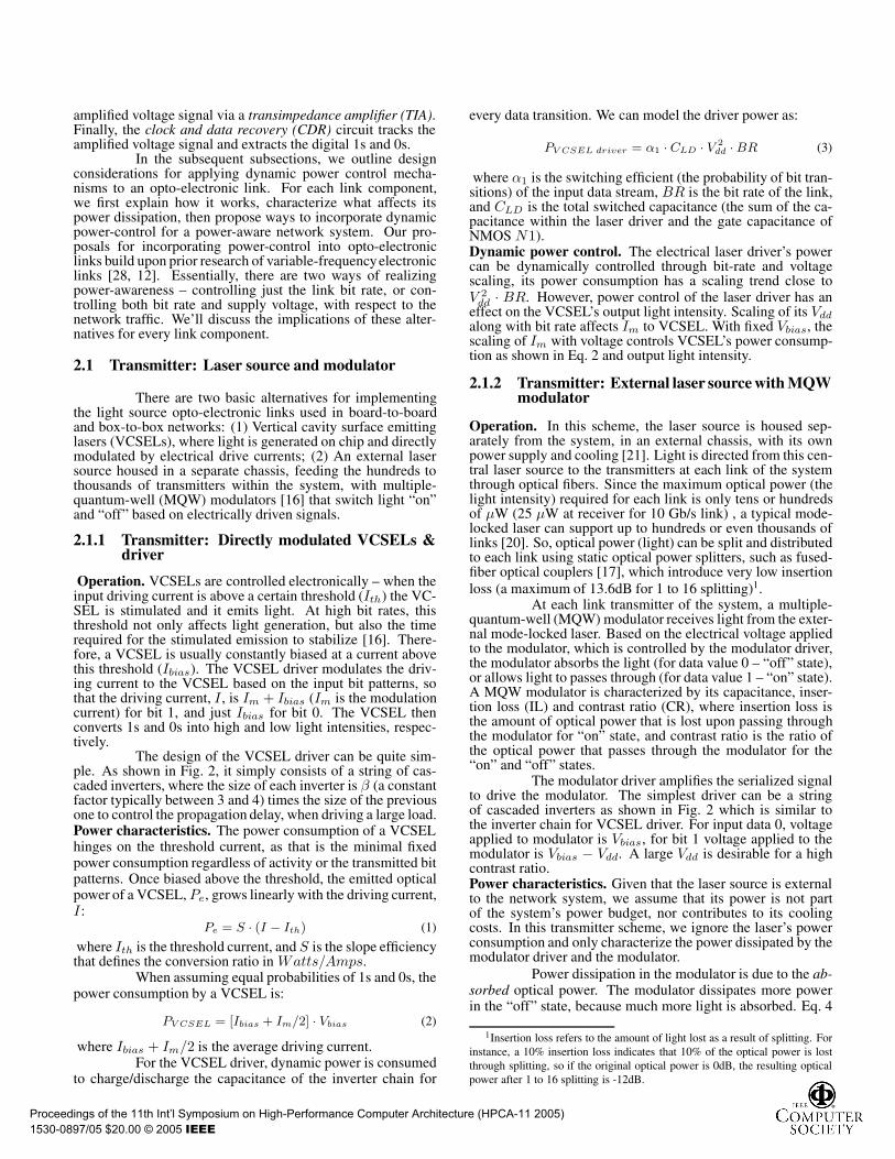
The design of the VCSEL driver can be quite sim-ple. As shown in Fig. 2, it simply consists of a string of cas-caded inverters, where the size of each inverter is β (a constantfactor typically between 3 and 4) times the size of the previousone to control the propagation delay, when driving a large load.Power characteristics. The power consumption of a VCSELhinges on the threshold current, as that is the minimal fixedpower consumption regardless of activity or the transmitted bitpatterns. Once biased above the threshold, the emitted opticalpower of a VCSEL, Pe, grows linearly with the driving current,I:
Pe = S · (I − Ith) (1)
where Ith is the threshold current, and S is the slope efficiencythat defines the conversion ratio in Watts/Amps.
When assuming equal probabilities of 1s and 0s, thepower consumption by a VCSEL is:
PV CSEL = [Ibias + Im/2] · Vbias (2)
where Ibias + Im/2 is the average driving current.For the VCSEL driver, dynamic power is consumed
to charge/discharge the capacitance of the inverter chain for
every data transition. We can model the driver power as:
PV CSEL driver = α1 · CLD · V 2dd · BR (3)
where α1 is the switching efficient (the probability of bit tran-sitions) of the input data stream, BR is the bit rate of the link,and CLD is the total switched capacitance (the sum of the ca-pacitance within the laser driver and the gate capacitance ofNMOS N1).Dynamic power control. The electrical laser driver’s powercan be dynamically controlled through bit-rate and voltagescaling, its power consumption has a scaling trend close toV 2
dd · BR. However, power control of the laser driver has aneffect on the VCSEL’s output light intensity. Scaling of its Vddalong with bit rate affects Im to VCSEL. With fixed Vbias, thescaling of Im with voltage controls VCSEL’s power consump-tion as shown in Eq. 2 and output light intensity.
2.1.2 Transmitter: External laser source with MQWmodulator
Operation. In this scheme, the laser source is housed sep-arately from the system, in an external chassis, with its ownpower supply and cooling [21]. Light is directed from this cen-tral laser source to the transmitters at each link of the systemthrough optical fibers. Since the maximum optical power (thelight intensity) required for each link is only tens or hundredsof µW (25 µW at receiver for 10 Gb/s link) , a typical mode-locked laser can support up to hundreds or even thousands oflinks [20]. So, optical power (light) can be split and distributedto each link using static optical power splitters, such as fused-fiber optical couplers [17], which introduce very low insertionloss (a maximum of 13.6dB for 1 to 16 splitting)1.
At each link transmitter of the system, a multiple-quantum-well (MQW) modulator receives light from the exter-nal mode-locked laser. Based on the electrical voltage appliedto the modulator, which is controlled by the modulator driver,the modulator absorbs the light (for data value 0 – “off” state),or allows light to passes through (for data value 1 – “on” state).A MQW modulator is characterized by its capacitance, inser-tion loss (IL) and contrast ratio (CR), where insertion loss isthe amount of optical power that is lost upon passing throughthe modulator for “on” state, and contrast ratio is the ratio ofthe optical power that passes through the modulator for the“on” and “off” states.
The modulator driver amplifies the serialized signalto drive the modulator. The simplest driver can be a stringof cascaded inverters as shown in Fig. 2 which is similar tothe inverter chain for VCSEL driver. For input data 0, voltageapplied to modulator is Vbias, for bit 1 voltage applied to themodulator is Vbias − Vdd. A large Vdd is desirable for a highcontrast ratio.Power characteristics. Given that the laser source is externalto the network system, we assume that its power is not partof the system’s power budget, nor contributes to its coolingcosts. In this transmitter scheme, we ignore the laser’s powerconsumption and only characterize the power dissipated by themodulator driver and the modulator.
Power dissipation in the modulator is due to the ab-sorbed optical power. The modulator dissipates more powerin the “off” state, because much more light is absorbed. Eq. 4
1Insertion loss refers to the amount of light lost as a result of splitting. Forinstance, a 10% insertion loss indicates that 10% of the optical power is lostthrough splitting, so if the original optical power is 0dB, the resulting opticalpower after 1 to 16 splitting is -12dB.
Proceedings of the 11th Int’l Symposium on High-Performance Computer Architecture (HPCA-11 2005)
1530-0897/05 $20.00 © 2005 IEEE
Tx MQW modulator
Vbias
Modulator driver
Serialized data
Vdd
RxPhoto
detector
Vbias
TIA
Vdd Reference fRf
current
CDRData
Clock
Voltage
Externallaser
Figure 1. Opto-electronic link architecture.
TxMQW
modulator
Vbias
Modulator driver
Input
Vdd
External Laser
TxVCSEL
Vbias
VCSEL driver
Vdd
Im Ibias
I
N1 N2 Vctr
(a) (b)
VgsInput
Figure 2. Alternatives for laser source and modulators. (a) An external laser source with an on-chip MQW modulator. (b) A directlymodulated VCSEL laser source.
shows the average power assuming the same probability of 1sand 0s.
Pmodulator = 0.5·Rs ·PI ·[IL·(Vbias−Vdd)+(1− 1 − IL
CR·Vbias)]
(4)where Rs is the conversion efficiency from optical power to
electrical current, PI the input optical power, Vbias the biasvoltage, and Vdd the supply voltage.
Again, modulator driver’s power consumption isdue to the charging/discharging of capacitances in the inverterchain. The maximum output voltage swing corresponds to thesupply voltage, so total power dissipation can be approximatedas:
Pmodulator driver = α2 · Cmd · V 2dd · BR (5)
where α2 is the switching efficiency (probability of bit transi-tions) of the input data stream, BR is the bit rate of the link,and Cmd is the total capacitance it drives (the sum of the ca-pacitance of the driver and the modulator).Dynamic power control. The modulator can be made power-aware by varying the light intensity delivered to each link byinserting a tunable attenuator after the splitter output for eachlink.
The electrical modulator driver can also be madepower-aware through bit-rate scaling. While scaling the sup-ply voltage with bit rate offers additional power savings, thatwould reduce the voltage swing to the modulator. This reduc-tion degrades the contrast ratio [7] making it harder to detectthe data at the receiver. Due to the already low supply voltagelevels, we opt to keep the supply voltage for modulator driverfixed. So, the power consumed by the modulator driver onlyscales with bit rate.
2.2 Receiver design
At the receiver, as shown in Fig. 1, the photode-tector accepts the light and converts the optical bit streamback into electrical current signals, which are then transformedinto amplified voltage signals by the transimpedance amplifier
(TIA). Finally, the clock and data recovery (CDR) circuit tracksthe amplified voltage signal and extracts the digital 1s and 0s.We explain the operation and real-time power-control of thesecomponents in detail in the following subsections.
2.2.1 Receiver: Photodetector
Operation. The photodetector converts the optical signalsinto photon-current. To guarantee an acceptable bit error rate(BER) (typical BER for inter-chassis and inter-board links is10−12), a minimum amount of optical power is required bythe detector, defined as the receiver sensitivity (Prec). Higherbit rates require higher receiver sensitivity to achieve the sameBER.Power characteristics. The detector dissipates power as it ab-sorbs photons to generate current. The average power dissipa-tion is shown in Eq. 6 [10]:
Pdetector = Prec · q
hν· Vbias · CR + 1
CR − 1(6)
where q is the charge of an electron, h is Planck constant, νis the optical frequency, and CR the optical intensity contrastratio for bit 1 and 0. Vbias is the bias voltage to the photode-tector.Dynamic power control. Given that the photodetector’spower dissipation is much lower than other components(<1mW [10]), no additional power control mechanisms areconsidered.
2.2.2 Receiver: Transimpedance amplifier (TIA)
Operation. The TIA typically consists of an internal common-source amplifier with a feedback impedance Rf as shown inFig. 1. It transforms the photon current (Ip) from the detectorto a voltage swing Ip · Rf . It works well up to a maximumbit rate (BRmax), which is regulated by the bias current of theinternal amplifier [1]:
Ibias = c · BRmax (7)
where c is a constant for a given TIA implementation.
Proceedings of the 11th Int’l Symposium on High-Performance Computer Architecture (HPCA-11 2005)
1530-0897/05 $20.00 © 2005 IEEE
Power characteristics. The power consumption for TIA de-pends on the bias current (Ibias), photon-current (Ip) and darkcurrent (Id) of the photo-detector [1]. However, as the powerincurred by the photon-current (less than 100µA) and dark cur-rent (several nA) are negligible [10], compared to the total TIApower consumption (around hundreds of mW) [1], the powerconsumed by TIA can be simplified as in Eq. 8:
PTIA = Ibias · Vdd = c · BRmax · Vdd (8)
Dynamic power control. When the bit rate scales down, themaximum affordable bit rate BRmax can be reduced by thesame degree. Thus, the bias current can scale with the bit-rate by tuning the supply voltage as the bias current has analmost linear relation to the supply current [19]. Then, theTIA’s power scales with Vdd · BR. Another benefit is that theTIA output voltage swing Ip · Rf can be smaller when supplyvoltage decreases. So with Rf fixed, less Ip is required for alower supply voltage.
2.2.3 Receiver: Clock and data recovery circuitry(CDR)
Operation. The CDR is a key component of both optical andelectrical receivers. It consists of a clock recovery circuit thatre-times an internal clock with respect to the incoming datasignals and decision circuitry that extracts digital data from thereceived signals. Once in lock, the CDR can recover a constantstream of data received at a fixed rate. However, in the event ofa sudden change in the bit rate, the CDR requires time (set bythe bandwidth of the timing recovery loop) to recapture lockbefore it can again operate reliably.Power characteristics. A straight forward implementation ofa CDR is to use a PLL (phase-locked loop) structure [12] . In aCDR, the PLL and clock buffers are the dominant power con-sumers, so power consumption does not change much with ac-tual bit patterns. Assuming CDRs are mostly comprised of dig-ital circuitry, the main power consumption comes from charg-ing and discharging capacitors at high frequency. Its powerconsumption can be approximated as:
PCDR = α3 · CCDR · V 2dd · BR (9)
where α3 is the switch efficient for CDR representing the prob-ability of charging or discharging the capacitance, CCDR is thecapacitance of the CDR.Dynamic power control. Like the VCSEL driver and the TIA,the CDR can similarly be frequency and voltage-scaled, as bitrate varies. Therefore, its power consumption has a scalingtrend close to V 2 ·f [12]. Whenever bit rate changes, we makethe conservative assumption that the CDR needs to relock tothe bit rate and re-synchronize the clock with the incomingdata, so it is disabled for a time period called bit-rate transitiondelay Tbr .
2.3 Design issues
Comparison of VCSELs vs. MQW modulatorswith an external laser. Due to its ease of integration withCMOS technologies, small footprint, and simpler connectiondesign over MQW modulators, VCSELs are commonly usedas the light source in box-to-box and board-to-board opto-electronic links. However, an external laser source coupledwith MQW modulators has also been proposed as an alterna-tive for such links [9] and offers some advantages. Here, we
compare the relative merits of using VCSELs versus MQWmodulators for a power-aware network, first considering vari-ous attributes of each scheme with respect to performance andpower. While this comparison is qualitative, Section 4 willevaluate both schemes using detailed network simulations toprovide a more quantitative comparison.
One advantage of using MQW modulators with anexternal laser source is that the technology has been exten-sively used for telecommunications. Hence, we can leverageexisting technology advancements, while VCSEL technologyis relatively immature. For example, current modulator-basedlinks have been demonstrated for 40 Gbps operation and be-yond [20]. In comparison, the highest modulation speed forVCSELs is still at 10GHz [18]. Another significant benefit ofusing MQW modulators can be derived from the stable opticalpower available from the external laser source. This stabil-ity offers relatively lower noise operation. Comparatively, theVCSEL output is sensitive to various factors such as temper-ature and the operating voltage environment, thus, requiringadditional circuit complexity to stabilize the system.
In addition to the performance benefits, modulator-based optical links has potential power advantages as well. Us-ing an external laser source allows us to move the primary heatsource in opto-electronic networked systems away (physically)from the actual system, into a separate chassis with its ownpower supply and cooling. This separation allows us to fo-cus on the network system’s power in order to ease thermalconstraints and only contend with the power dissipation asso-ciated with the MQW modulators in the overall system powerbudget.
While one of the disadvantages of VCSELs stemsfrom the threshold current that consumes constant power, re-cent progress in in VCSEL technology, such as oxide-aperture-confined structure [18, 10], has significantly reduced thethreshold current to hundreds of micro-amps. Thus, for theon-board power dissipation, VCSEL based transmitters dissi-pate power comparable to MQW modulator based transmitters[10]. Moreover, there is lower complexity to build and controla VCSEL based power-aware opto-electronic link. So, bothschemes are explored in this paper and their relative efficiencyin adjusting network power consumption with respect to trafficis simulated and explored in Section 4.
Interaction between power-control mechanismsand operation of link components. Implementing power con-trol into the various link components of a power-aware networkrequires careful consideration of its interaction with the com-ponents. When bit rate scales down, also reducing the supplyvoltage to each of the components (e.g., VCSEL/modulatordriver, TIA, and CDR) offers significant power savings, asshown by Eqs. 3, 5, 8 and 9. However, if the output swing ofthe modulator driver (set by the power supply voltage) drops,there will be a dramatic increase in insertion loss and a big de-crease in contrast ratio. Those effects will adversely affect thephotodetector’s operation. Therefore, only bit rate (frequency)control can be used to reduce power consumption in the mod-ulator driver.
In contrast, for a VCSEL-based transmitter, both bitrate and supply voltage can be controlled, as a decrease in mod-ulation current (due to a lower supply voltage) only leads to alinear reduction in the optical output power, preserving a highcontrast ratio. Moreover, both the photodetector and TIA areable to operate at lower light levels and supply voltages as bitrate decreases. Hence, it is possible to maintain acceptableBER performance by carefully balancing the impact of lowerlight intensity.
These simple examples show that the power-controlmechanisms (i.e., frequency and voltage control) in each com-
Proceedings of the 11th Int’l Symposium on High-Performance Computer Architecture (HPCA-11 2005)
1530-0897/05 $20.00 © 2005 IEEE
ponent of an opto-electronic link have to work in concert, inorder to allow link power consumption to vary with bit rateswhile ensuring correct operation. These nuances are factoredinto our overall networked system design and simulated to fa-cilitate a quantitative exploration of the design space of power-aware opto-electronic networks.
3 Power-aware opto-electronic networked sys-tem
Advances in VLSI and network link bandwidths aremaking it cost-effective to connect multiple processing ele-ments to each communication router, forming clustered sys-tems. While flat interconnection network architectures aretraditionally assumed, hierarchical, clustered architectures aregaining interest in large scalable parallel systems–examplesinclude the IBM Blue Gene [5], Intel Paragon [8], StanfordDASH [15], and Cray T3D [3]. We thus target such systemswith power-awareness using power-controlled opto-electroniclinks, as proposed in the previous section, for both inter-rackas well as inter-board interconnections.
3.1 System architecture
In this section, we present in detail an example sys-tem architecture using MQW-modulator-based links, owing totheir higher complexity. A network system with VCSEL-basedlinks is similar to the example system except that no externallaser source is required. Moreover, light intensity is controlleddirectly by the VCSEL driver instead of requiring external op-tical power control.
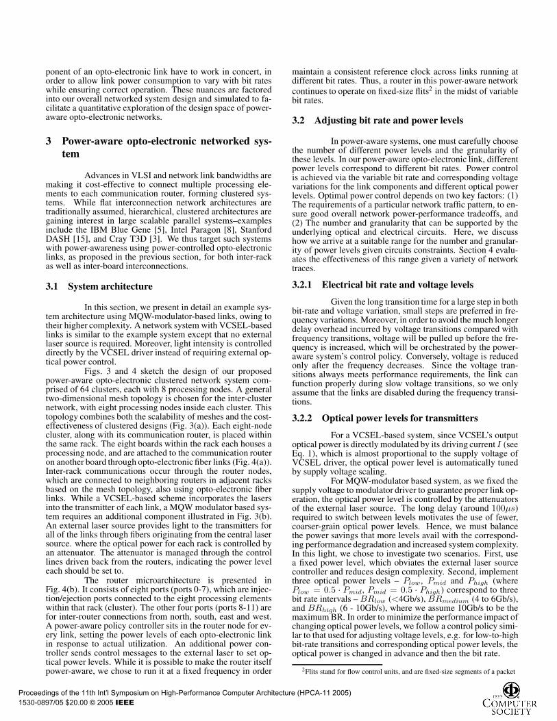
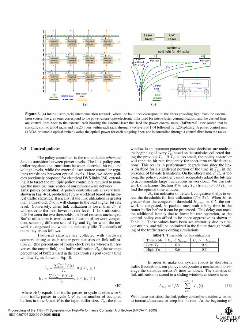
Figs. 3 and 4 sketch the design of our proposedpower-aware opto-electronic clustered network system com-prised of 64 clusters, each with 8 processing nodes. A generaltwo-dimensional mesh topology is chosen for the inter-clusternetwork, with eight processing nodes inside each cluster. Thistopology combines both the scalability of meshes and the cost-effectiveness of clustered designs (Fig. 3(a)). Each eight-nodecluster, along with its communication router, is placed withinthe same rack. The eight boards within the rack each houses aprocessing node, and are attached to the communication routeron another board through opto-electronic fiber links (Fig. 4(a)).Inter-rack communications occur through the router nodes,which are connected to neighboring routers in adjacent racksbased on the mesh topology, also using opto-electronic fiberlinks. While a VCSEL-based scheme incorporates the lasersinto the transmitter of each link, a MQW modulator based sys-tem requires an additional component illustrated in Fig. 3(b).An external laser source provides light to the transmitters forall of the links through fibers originating from the central lasersource. where the optical power for each rack is controlled byan attenuator. The attenuator is managed through the controllines driven back from the routers, indicating the power leveleach should be set to.
The router microarchitecture is presented inFig. 4(b). It consists of eight ports (ports 0-7), which are injec-tion/ejection ports connected to the eight processing elementswithin that rack (cluster). The other four ports (ports 8-11) arefor inter-router connections from north, south, east and west.A power-aware policy controller sits in the router node for ev-ery link, setting the power levels of each opto-electronic linkin response to actual utilization. An additional power con-troller sends control messages to the external laser to set op-tical power levels. While it is possible to make the router itselfpower-aware, we chose to run it at a fixed frequency in order
maintain a consistent reference clock across links running atdifferent bit rates. Thus, a router in this power-aware networkcontinues to operate on fixed-size flits2 in the midst of variablebit rates.
3.2 Adjusting bit rate and power levels
In power-aware systems, one must carefully choosethe number of different power levels and the granularity ofthese levels. In our power-aware opto-electronic link, differentpower levels correspond to different bit rates. Power controlis achieved via the variable bit rate and corresponding voltagevariations for the link components and different optical powerlevels. Optimal power control depends on two key factors: (1)The requirements of a particular network traffic pattern, to en-sure good overall network power-performance tradeoffs, and(2) The number and granularity that can be supported by theunderlying optical and electrical circuits. Here, we discusshow we arrive at a suitable range for the number and granular-ity of power levels given circuits constraints. Section 4 evalu-ates the effectiveness of this range given a variety of networktraces.
3.2.1 Electrical bit rate and voltage levels
Given the long transition time for a large step in bothbit-rate and voltage variation, small steps are preferred in fre-quency variations. Moreover, in order to avoid the much longerdelay overhead incurred by voltage transitions compared withfrequency transitions, voltage will be pulled up before the fre-quency is increased, which will be orchestrated by the power-aware system’s control policy. Conversely, voltage is reducedonly after the frequency decreases. Since the voltage tran-sitions always meets performance requirements, the link canfunction properly during slow voltage transitions, so we onlyassume that the links are disabled during the frequency transi-tions.
3.2.2 Optical power levels for transmitters
For a VCSEL-based system, since VCSEL’s outputoptical power is directly modulated by its driving current I (seeEq. 1), which is almost proportional to the supply voltage ofVCSEL driver, the optical power level is automatically tunedby supply voltage scaling.
For MQW-modulator based system, as we fixed thesupply voltage to modulator driver to guarantee proper link op-eration, the optical power level is controlled by the attenuatorsof the external laser source. The long delay (around 100µs)required to switch between levels motivates the use of fewer,coarser-grain optical power levels. Hence, we must balancethe power savings that more levels avail with the correspond-ing performance degradation and increased system complexity.In this light, we chose to investigate two scenarios. First, usea fixed power level, which obviates the external laser sourcecontroller and reduces design complexity. Second, implementthree optical power levels – Plow, Pmid and Phigh (wherePlow = 0.5 · Pmid, Pmid = 0.5 · Phigh) correspond to threebit rate intervals – BRlow (<4Gb/s), BRmedium (4 to 6Gb/s),and BRhigh (6 - 10Gb/s), where we assume 10Gb/s to be themaximum BR. In order to minimize the performance impact ofchanging optical power levels, we follow a control policy simi-lar to that used for adjusting voltage levels, e.g. for low-to-highbit-rate transitions and corresponding optical power levels, theoptical power is changed in advance and then the bit rate.
2Flits stand for flow control units, and are fixed-size segments of a packet
Proceedings of the 11th Int’l Symposium on High-Performance Computer Architecture (HPCA-11 2005)
1530-0897/05 $20.00 © 2005 IEEE
Light provider
Inter-router linksControl infor
20 fibers
Rack with 8 nodes and one router
20fibers
Rack with 8 nodes and one router
20fibers
Rack with 8 nodes and one router
20 fibers
Rack with 8 nodes and one router
20fibers
Rack with 8 nodes and one router
20fibers
Rack with 8 nodes and one router
20 fibers
Rack with 8 nodes and one router
20fibers
Rack with 8 nodes and one router
20fibers
Rack with 8 nodes and one router
20 fibers
Rack with 8 nodes and one router
20 fibers
Rack with 8 nodes and one router
20 fibers
Rack with 8 nodes and one router
LaserDriver
CWLaser
splitter to split light for 64 racks
1 to 20 splitter &20 VOAs
For rack 63
0
For rack 1
19
0
1279
0
63
Light provider
Controlinfor
1 63
1 to 20 splitters
VOA 0
VOA 1
VOA19
1 to 20 de-
multi-plexer
190 1
0 1 19
(a) (b)
Figure 3. (a) Inter-cluster (rack) interconnection network, where the bold lines correspond to the fibers providing light from the externallaser source, the gray ones correspond to the power-aware opto-electronic links used for inter-cluster communication, and the dashed linesare control lines back to the external rack housing the external laser that feed the power control units, (b)External laser source that isstatically split to all 64 racks and the 20 fibers within each rack, through two levels of 1:64 followed by 1:20 splitting. A power control unit(a VOA or tunable optical switch) varies the optical power for each outgoing fiber, and is controlled through a control fiber from the racks.
3.3 Control policies
The policy controllers in the router decide when andhow to transition between power levels. The link policy con-troller regulates the transitions between electrical bit rate andvoltage levels, while the external laser source controller regu-lates transitions between optical levels. Here, we adopt poli-cies previously proposed for electrical DVS links [24], extend-ing it to target the multiple policy controllers required to man-age the multiple time scales of our power-aware network.Link policy controller. A policy controller sits at every link,shown in Fig. 4(b), predicting future workload based on histor-ical traffic statistics. Basically, if the link utilization is greaterthan a threshold, TH , it will change to the next higher bit ratelevel. Conversely, when link utilization is lower than TL, itwill move to the next lower bit rate level. If link utilizationfalls between the two thresholds, the level remains unchanged.Buffer utilization is used as an indication of network conges-tion, selecting different sets of TH and TL for when the net-work is congested and when it is relatively idle. The details ofthe policy are as follows.
Historical statistics are collected with hardwarecounters sitting at each router port–statistics on link utiliza-tion Lu (the percentage of router clock cycles where a flit tra-verses the output link) and buffer utilization Bu (the averagepercentage of buffers used in the next router’s port) over a timewindow Tw as shown in Eq. 10.
Lu =
PTw−1t=0 A(t)
Tw, 0 ≤ Lu ≤ 1
Bu =
PTw−1t=0 F (t)/B
Tw, 0 ≤ Bu ≤ 1
(10)
where A(t) equals 1 if traffic passes in cycle t, otherwise 0if no traffic passes in cycle t, Ft is the number of occupiedbuffers in time t, and B is the input buffer size. Tw, the time
window, is an important parameter, since decisions are made atthe beginning of every Tw based on the statistics collected dur-ing the previous Tw. If Tw is too small, the policy controllerwill tune the bit rate frequently for short-term traffic fluctua-tions. This results in performance degradations since the linkis disabled for a significant portion of the time in Tw, in thepresence of bit-rate transitions. On the other hand, if Tw is toolong, the policy controller cannot adequately adapt the bit-rateto accommodate large fluctuations in workload. We use net-work simulations (Section 4) to vary Tw (from 5 to 500 Tbr) tofind the optimal time window.
Bu (an indicator of network congestion) helps to se-lect the thresholds for link utilization (TH , TL). When Bu isgreater than the congestion threshold Bu,con = 0.5, the net-work is congested, so packets must wait a long time in therouter buffer before it can be processed. This delay can maskthe additional latency due to lower bit rate operation, so thecontrol policy can afford to be more aggressive as shown inTable 1. These values have been set arbitrarily due to timeconstraints, and will be optimized in the future through profil-ing of the traffic traces during simulations.
Table 1. Thresholds for link utilizationThresholds Bu < Bu,con Bu >= Bu,con
Low, TL 0.4 0.6High, TH 0.6 0.7
In order to make our system robust to short-termtraffic fluctuations, our policy incorporates a mechanism to av-erage the statistics across N time windows. The statistics oflink utilization is stored in a sliding window, as shown here:
Lu,a = 1/N ·i=N−1∑
i=0
Lu(i) (11)
With these statistics, the link policy controller decides whetherto increase/decrease or keep the bit-rate. At the beginning of
Proceedings of the 11th Int’l Symposium on High-Performance Computer Architecture (HPCA-11 2005)
1530-0897/05 $20.00 © 2005 IEEE
Router
Node 3
Node 2
Node 1
Node 0
32
10
Node 7
Node 6
Node 5
Node 4
45
67
11
910
8
20 fibers
Light provider
Inter-router links
Links for injection/ejection
Control infor
CrossbarSwitch
Routing0
9
10
11
0
8
9
10
11
8
7 7
Rx8
Rx9
Rx11
Rx10
Rxsfor 8 inject ports
Tx8
Tx9
Tx10
Tx11
Txsfor 8 eject ports
External light source Controller
Light provider
Inter-router links
Control infor
Links for injection/ejection
Input buffer
Input buffer
Input buffer
Input buffer
Output buffer
Output buffer
Output buffer
Output buffer
Policy controller
Policy controller
Policy controller
Policy controller
Output buffers
Input buffers
Policy controllers for ejection ports
(a) (b)
Figure 4. (a) Sketch of the internals of a rack, consisting of eight boards, each with a processing node, and the communication routerboard, (b) Router micro-architecture, with 8 injection and ejection ports to the intra-rack cluster, and 4 ports with two uni-directional linksfor inter-rack communications.
every Tw, Lu,a is compared with two link utilization thresh-olds (TH , TL). When Lu,a is greater than TH , the policy con-troller increases bit rate by one level, Similarly, when Lu,a islower than TL, the bit rate will decrease by a step. If Lu,afalls between the two thresholds, bit rate does not change. Fora modulator-based system with multiple optical power levels,the link policy controller cooperates with the external lasersource controller, which is described next.External laser source controller for modulator-based sys-tems. To accommodate the long transition/response times ofthe attenuators at the external laser source, the external lasersource controller seeks to track much longer trends in networktraffic. Since the response time of the attenuators is around100µs, the link policy controller will decide whether to changethe optical power levels every 200µs. If in this 200µs, the bitrate always remains at a power level that can function witha lower optical power, the policy controller will send a Pdecrequest, which triggers the external laser source controller totell the external laser source to halve its optical power. On theother hand, if the link policy controller needs to increase linkbit rate above that which can be supported by the current op-tical power level, it will instantly send a Pinc request to theexternal laser source controller (with the electrical bit-rate andvoltage remaining constant until the optical power increases),which will prompt a doubling of the optical power. Otherwise,the input optical power remains fixed.
4 Evaluation results
To evaluate the performance impact and potentialpower savings of power-aware opto-electronic networks, wesimulate the details of the entire power-aware network systemas described in the previous two sections. Here, we present thesimulation setup and experimental findings.
4.1 Network simulator & experimental setup
An event-driven flit-level interconnection networksimulator [23] with 5-stage pipelined routers was modified
to include the detailed power-performance characteristics ofa power-aware opto-electronic link, the external laser sourcewith attenuators, the routers with the policy controllers, model-ing a complete 64-rack power-aware networked system. In ourexperiments, the routers run at 625MHz, have 16 flits buffersper input port, where each flit is 16 bits wide. The maximumbandwidth out of each input port is set to be 10Gb/s. Thesimulator can be configured to model either VCSEL-based orMQW-modulator-based opto-electronic links.
Separate clock domains are used for the router coreand its links. Functional modules inside the router core op-erate off of a fixed system clock, while each link has its ownclock dynamically tuned by the link policy controller to followthe traffic changes. In the MQW-modulator-based links withmultiple optical power levels, the external laser source policycontroller in each router dynamically controls the attenuatorsin the external chassis.
The power consumption for the various componentsof an opto-electronic link is estimated using the power modelsdescribed in Section 2, based on parameters from [1, 2, 13],assuming 0.18µm CMOS technology is used to implement allof the link circuitry. A rough breakdown of the power con-sumed for various link components operating at the maximumbit rate of 10Gb/s is listed in Table 2, along with approxi-mate power-scaling trends for each component derived fromthe power models presented in Section 2. We assume that therequired supply voltage to the VCSEL driver, TIA, and CDRwill linearly scale with bit rate [12, 28], while the modulatordriver’s voltage is fixed to ensure correct operation.
As shown in Table 2, the transmitter of our uni-directional 10Gb/s opto-electronic link takes approximately40mW, while the receiver dissipates approximately 250mW,a total of 290mW per link. With bit rate scaling from 10Gb/sto 5Gb/s with 6 bit-rate levels, the supply voltage scales from1.8V to 0.9V accordingly, excluding the supply voltage tothe modulator driver. This lowers link power consumption to61.25mW at 5Gb/s for a VCSEL-based links, allowing a po-tential power savings of about 80%.
To be conservative, the link will be disabled for
Proceedings of the 11th Int’l Symposium on High-Performance Computer Architecture (HPCA-11 2005)
1530-0897/05 $20.00 © 2005 IEEE
Table 2. Power consumptions and scaling trends of the link components.VCSEL VCSEL driver Modulator driver TIA CDR
Power (mW) 30 10 40 100 150Scaling trend ∼ Vdd V 2
dd · BR BR Vdd · BR V 2dd · BR
20 network cycles3 after the bit-rate transitions to give theCDR time to relock the clock to the input data. The tran-sitions of supply voltage is slower, taking 100 network cy-cles. These delays are estimated and extrapolated based oncharacterizations of prior circuit designs of variable-frequencylinks [28, 12]. The impact of these transition delays will beinvestigated through network simulations.
Latency, throughput, power dissipation, and power-latency product are the metrics used to evaluate our power-aware policies. Latency refers to the time from the creation ofthe first flit of the packet till the ejection of its last flit fromthe network at the destination, throughput is defined as the in-jection rate at which average network latency exceeds twicethe latency at zero network load, and the power dissipated byour power aware network is expressed as a percentage of thatconsumed by a non-power-aware network with all links at themaximum bit rate of 10Gb/s. Averages are computed acrossall nodes in the network. Power-latency product multiplies av-erage latency with average power dissipation, encapsulating ina single metric the power-performance of a network.
4.2 Workloads
Network workloads that accurately reflect the hightemporal and spatial traffic variance of many applications, withdynamic fluctuations, bursts and hot-spots, are most useful forevaluating the performance of our power-aware network de-sign. In this paper, we present results for three sets of traces:(1) Uniform random traffic, where each node has equal proba-bility of sending to any other node, at a constant injection rate;(2) A time-varying hot-spot traffic trace, where packets are in-jected at different injection rates at different phases of the sim-ulation (temporal variance), and node 4 in rack(3,5) acceptsfour times the traffic injected into others (spatial variance); (3)Actual traffic traces extracted from SPLASH2 parallel applica-tions [29] running on the RSIM multiprocessor simulator withdefault parameters [27].
Uniform random traffic is one of the most widely-used network loads due to its simplicity that lends readilyto analysis. For power-aware networks, its constant injec-tion rate poses a worst-case scenario to the policy controller,since the lack of variance provides little opportunity for fre-quency/voltage scaling. We thus use it to stress our power-aware policies. The time-varying hotspot trace is used to eval-uate the responsiveness of our power-aware network designto fairly marked fluctuations in network traffic, essentially tostress our power-aware circuit mechanisms, highlighting theimpact of link circuitry overheads. The SPLASH traffic tracesare used to evaluate the realistic power-performance impact ofa power-aware network.
4.3 Simulation results and performance evaluation
4.3.1 Uniform random traffic
Effect of policy parameters. We first explore the impact ofour policy’s sampling window size (Tw), i.e. how frequentlyit samples statistics, on a modulator-based network (trends are
3A network cycle is basically one flit time.
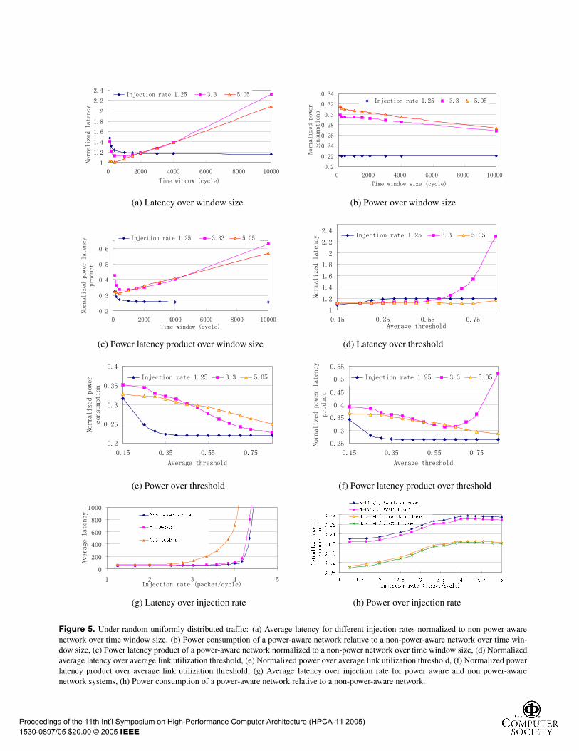
similar for VCSEL-based networks), varying it from 100 to10000 cycles.
Fig. 5(a) presents the average network latency (av-eraged across all links in the network) relative to that of a nonpower aware network under light (1.25 packets/cycle), medium(3.3 packets/cycle) and heavy (5 packets/cycle) injection rates.It shows that a larger latency penalty is incurred for the short-est windows (Tw = 100). This is because a control pol-icy that uses shorter windows yields more power-level tran-sitions, which in turn incurs more transition penalties. Largerlatency penalty is also incurred for a bigger window size un-der medium and heavy traffic since it cannot respond quicklyto traffic variations. The effect on power dissipation (seeFig. 5(b)) shows shorter time windows leading to higher powerconsumption for all traffic injection rates except under 1.25packets/cycle. At such light traffic, the power-aware networkessentially transitions to the lowest bit-rate supported (5Gb/s)and remains at that level. Fig. 5(c) presents the effect of win-dow size on power-latency product. It shows that window sizearound 1000 cycles yields acceptable power latency productfor all injection rates. While one might expect a shorter timewindow to enable the policy to be more responsive, better tracktraffic fluctuations, and thus reduce power, more frequent bit-rate transitions also lead to higher power consumptions. Sincethe network must disable the links more often, it must com-pensate for this loss in link activity with higher bit rates whenlinks are active, resulting in higher power consumption. Basedon these results, we choose Tw = 1000 cycles for all subsequentsimulations.
Figs. 5(d),(e),(f) present the effect of link utilizationthresholds (TH and TL) on average latency, power consump-tion and power-latency product, respectively. The differencebetween high and low utilization thresholds (TH −TL) is fixedat 0.1 as simulations show better power-performance. Intu-itively, higher thresholds lead to more aggressive scaling oflink bit rates, which result in larger delays as well as lowerpower consumption, as is evident for the injection rate of 3.3packets/cycle. At light traffic (1.25 packets/cycle), the power-aware network relegates to few transitions – mimicking a net-work whose link bit rates are statically set at startup. Athigh traffic (5.05 packets/cycle), network latency does not in-crease either with more aggressive thresholds, as the network ishighly congested, so flits are queued up in the routers for longperiods of time anyway, masking the additional link delay dueto power-aware networks. We choose an average threshold of0.5 for subsequent simulations in order to balance the impacton power-performance. If a larger average threshold of 0.6 ischosen, higher power savings can be attained, demonstratingthe tradeoff designers have to make.Effect of link technology. Fig 5(g) compares the average la-tency of two power-aware network configurations – one whoselink bit rates vary from 5 to 10Gb/s, vs. one whose link bit ratesvary from 3.3 to 10Gb/s. Our simulations show the networkwith 5-10Gb/s links not hurting network throughput, saturatingat the same point as the non-power-aware network. When 3.3-10Gb/s links are used, however, throughput suffers, degrad-ing to about 3 packets/cycle. If link bit rates are statically setat 3.3Gb/s, throughput will be severely affected, dropping tolower than 2 packets/cycle.
Fig. 5(h) presents the average power consumptionof power-aware network systems. Power savings can be at-
Proceedings of the 11th Int’l Symposium on High-Performance Computer Architecture (HPCA-11 2005)
1530-0897/05 $20.00 © 2005 IEEE
�
���
���
���
���
�
���
���
� ���� ���� ���� ���� �����
��� ��� ��������
������������ ��
������������������ ��� ����
���
����
����
����
����
���
����
����
� ���� ���� ���� ���� �����
�� ����� ��� �������
����������� �
������������
�������� ���� ���� ��� ����
(a) Latency over window size (b) Power over window size
���
���
���
���
���
� ���� ���� ���� ���� ������ ������������� �
����������� ��������
������
��� ��������� ����� ���� �����
�
���
���
���
���
�
���
���
���� ��� ���� ����� ��� ���� �����
������������ �� ��� ��������� ����� � ����
(c) Power latency product over window size (d) Latency over threshold
���
����
���
����
���
���� ���� ���� ����
�� ������������
����������� �
�����������
����������� ������� ��� ����
����
���
����
���
����
���
����
���� ���� ���� ����
�� ������������
����������� ��������
������
����������� ������� ��� ����
(e) Power over threshold (f) Power latency product over threshold
�
���
���
���
���
����
� � � � ��� ������������ ���� � ���
������������� ���������������
�� ���
����� ���
����
����
����
���
����
����
����
� ��� � ��� � ��� � ��� ��� ������������ ���� � ���
��������������
����������
����������� ����������
�������������������
������������� ����������
���������������������
(g) Latency over injection rate (h) Power over injection rate
Figure 5. Under random uniformly distributed traffic: (a) Average latency for different injection rates normalized to non power-awarenetwork over time window size. (b) Power consumption of a power-aware network relative to a non-power-aware network over time win-dow size, (c) Power latency product of a power-aware network normalized to a non-power network over time window size, (d) Normalizedaverage latency over average link utilization threshold, (e) Normalized power over average link utilization threshold, (f) Normalized powerlatency product over average link utilization threshold, (g) Average latency over injection rate for power aware and non power-awarenetwork systems, (h) Power consumption of a power-aware network relative to a non-power-aware network.
Proceedings of the 11th Int’l Symposium on High-Performance Computer Architecture (HPCA-11 2005)
1530-0897/05 $20.00 © 2005 IEEE
tained even when the inter-router links are completely satu-rated, as the injection/ejection links into the cluster router arelowly utilized for uniform random traffic. Before network sat-uration, power dissipation increases as more traffic is injected.Beyond that, the power-aware policy controller can be moreaggressive in adjusting bit rates to enable more power sav-ings even as traffic increases. It shows that power aware opto-electronic networks are more effective at light and heavy endsof traffic conditions where sensitivity of overall network la-tency to link delay is lower.
It is again important to point out that more powersavings is also achievable at the expense of increased la-tency penalty by using a lower minimum bit-rate as shown inFig 5(g),(h). These plots clearly demonstrate the tradeoff be-tween latency and power savings for power-aware networks.If power consumption is our main concern, greater than 90%savings in power consumption can be achieved, with VCSEL-based networks having a slight advantage. We select 5-10Gb/srange henceforth since that gives better power-performance.
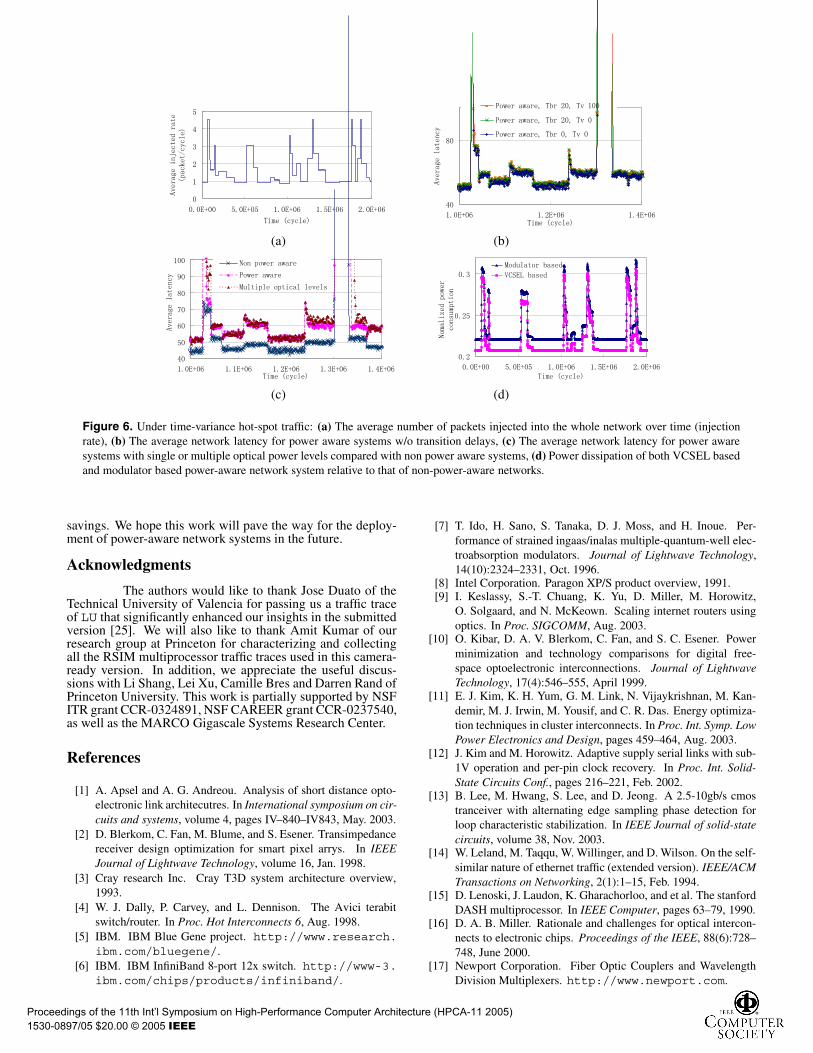
4.3.2 Time-varying hot-spot traffic
Fig. 6 presents the network simulation results usingthe time-varying hotspot traffic trace shown in Fig. 6(a).Effect of link circuitry constraints. The number and range ofbit-rate (and corresponding voltage) levels and transition de-lays between levels are key link circuitry constraints that im-pact overall network performance. Having an understandingof their effect on overall network performance allows a linkdesigner to better tune its link specifications.
To explore the effect of transition delay overheads,we zero out Tv and/or Tbr. As expected, Fig. 6(b) and (c)shows that a system without power awareness has the lowestlatency, since all of the links operate at the highest bit rate,and thus consume the most power. Given the control policyof changing the supply voltage in advance of increasing thebit rate, links are able to always operate in the presence ofvoltage transitions. Hence, the voltage transition penalty hasnegligible impact on performance. These results also show thatfor a timing window size (Tw) of 1000 cycles, the relativelysmall penalty of disabling the link for 20 cycles during bit-transitions (Tbr) has little impact on performance.VCSEL vs. MQW modulator-based power-aware links.Fig. 6(c) provides insights into the impact of multiple opticalpower levels for a network with MQW modulators. For smallincreases in the network traffic (from 1.1e6 to 1.3e6 cycles),which corresponds to a small increase in bit rate, the opticalpower level does not change and there is no additional latencypenalty. However, for a larger jump (between 1e6 and 1.1e6cycles), a change in the optical power level is triggered, incur-ring higher latency as the network has to wait 100µs for anoptical power transition. These simulation results verify thatchoosing a smaller number of coarse-grain optical power lev-els yields lower latency penalties. While this additional delaypenalty is infrequent, subsequent simulations assume a singleoptical level to simplify comparisons between systems usingVCSELs and MQW modulators.
Given these promising results, Fig. 6(d) then com-pares the normalized power consumption for systems usingVCSELs versus MQW modulators, relative to non-power-aware networks. The slight advantage of a VCSEL-based sys-tem stems from the fact that its laser driver’s power can scalewith both bit rate and voltage, while the modulator driver op-erates off of a fixed supply voltage and only scales with bitrate.
4.3.3 Traffic traces of SPLASH2 parallel bench-marks on RSIM
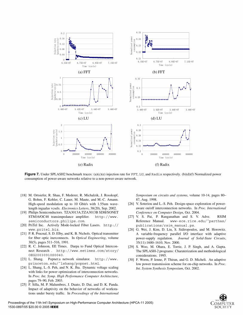
Three SPLASH2 benchmarks are used to evaluateour power-aware network – fast fourier transform (FFT), ma-trix decomposition (LU), integer sort kernel (Radix). Thebenchmarks are parallelized onto 64 nodes housed in 8 racksof our proposed networked system. Since traces are long (sev-eral hundreds of millions of cycles), we snapshot just a por-tion where large fluctuations in injection rate are seen (Fig. 7).Figs. 7(a)(c)(e) show the injection rate over time (the averagepacket size is 48-flit) while Figs. 7(b)(d)(f) present the powerconsumption of the modulator-based power aware system un-der those 3 traces normalized to the power of non power awaresystem. We see that our power-aware network tracks work-load fluctuations effectively. In addition, since link bit-rate isonly changed for big variations in link utilization, the powercurves filter out small fluctuations in the injection rate curvesand are thus smoother. On average, more than 75% savingsin power consumption is achieved with less than double net-work latency, resulting in more than 60% savings in networkpower latency product as shown in Table 3. The latency im-pact for FFT is much lower than the others as its traffic peaksand troughs occur over a longer period of time, making it eas-ier for the policy to accurately predict trends. The increase inthis raw network transmission latency needs to be taken in thecontext of overall network delay, which includes hundreds andthousands of cycles of network interface and software latency.
Table 3. Power-performance numbers for power aware net-works normalized against non-power-aware networks.
Traces FFT LU RadixAverage latency 1.08 1.50 1.60Average power consumption 0.22 0.25 0.23Average power latency product 0.24 0.38 0.37
5 Conclusions
In this paper, we explored the design space ofpower-aware opto-electronic networks. To the best of ourknowledge, this is the first complete power-aware network de-sign that explores link circuits, router microarchitecture, andoverall network system architecture in tandem, as well as thefirst proposal of a detailed power-aware link architecture. Jointinvestigation across these areas allow link constraints to beaccurately factored into network design, and system require-ments to be incorporated into the underlying circuit design pro-cess.
Through detailed network simulations with bothsynthetic and actual traces, we show that power-aware opto-electronic networks can lower power consumption by approx-imately 4×, with VCSEL-based power-aware opto-electroniclinks consistently turning in slightly better power-performanceacross all traces. Moreover, this simulation environment hasenabled us to understand the impact of various control param-eters and design choices on power and performance, and findoptimal settings.
We are currently working towards the design ofopto-electronic link components implemented in a 0.18µmCMOS process with power-control capabilities that are com-patible to the proposed power-aware network. Experimentalresults extracted from the test-chip prototype can then be fedinto our network system simulator, in place of current mod-els, to more accurately evaluate system performance and power
Proceedings of the 11th Int’l Symposium on High-Performance Computer Architecture (HPCA-11 2005)
1530-0897/05 $20.00 © 2005 IEEE
�
�
�
�
�
�
������ ������ ����� ����� �����
�� ���������
������������� �����
��������������
��
��
������� ������ ��������� ������ �
�������������
��� ������ �������������
��� ������ �����������
��� ������ �����������
(a) (b)
��
��
��
��
��
��
���
����� ����� ����� � ��� �����������������
�������������
���������������
�����������
!�"�������"�������#��$
���
����
���
������� ������� ������ ������ ������
�� ������ �
������������
�����������
������������� �
���� ���� �
(c) (d)
Figure 6. Under time-variance hot-spot traffic: (a) The average number of packets injected into the whole network over time (injectionrate), (b) The average network latency for power aware systems w/o transition delays, (c) The average network latency for power awaresystems with single or multiple optical power levels compared with non power aware systems, (d) Power dissipation of both VCSEL basedand modulator based power-aware network system relative to that of non-power-aware networks.
savings. We hope this work will pave the way for the deploy-ment of power-aware network systems in the future.
Acknowledgments
The authors would like to thank Jose Duato of theTechnical University of Valencia for passing us a traffic traceof LU that significantly enhanced our insights in the submittedversion [25]. We will also like to thank Amit Kumar of ourresearch group at Princeton for characterizing and collectingall the RSIM multiprocessor traffic traces used in this camera-ready version. In addition, we appreciate the useful discus-sions with Li Shang, Lei Xu, Camille Bres and Darren Rand ofPrinceton University. This work is partially supported by NSFITR grant CCR-0324891, NSF CAREER grant CCR-0237540,as well as the MARCO Gigascale Systems Research Center.
References
[1] A. Apsel and A. G. Andreou. Analysis of short distance opto-electronic link architecutres. In International symposium on cir-cuits and systems, volume 4, pages IV–840–IV843, May. 2003.
[2] D. Blerkom, C. Fan, M. Blume, and S. Esener. Transimpedancereceiver design optimization for smart pixel arrys. In IEEEJournal of Lightwave Technology, volume 16, Jan. 1998.
[3] Cray research Inc. Cray T3D system architecture overview,1993.
[4] W. J. Dally, P. Carvey, and L. Dennison. The Avici terabitswitch/router. In Proc. Hot Interconnects 6, Aug. 1998.
[5] IBM. IBM Blue Gene project. http://www.research.ibm.com/bluegene/.
[6] IBM. IBM InfiniBand 8-port 12x switch. http://www-3.ibm.com/chips/products/infiniband/.
[7] T. Ido, H. Sano, S. Tanaka, D. J. Moss, and H. Inoue. Per-formance of strained ingaas/inalas multiple-quantum-well elec-troabsorption modulators. Journal of Lightwave Technology,14(10):2324–2331, Oct. 1996.
[8] Intel Corporation. Paragon XP/S product overview, 1991.[9] I. Keslassy, S.-T. Chuang, K. Yu, D. Miller, M. Horowitz,
O. Solgaard, and N. McKeown. Scaling internet routers usingoptics. In Proc. SIGCOMM, Aug. 2003.
[10] O. Kibar, D. A. V. Blerkom, C. Fan, and S. C. Esener. Powerminimization and technology comparisons for digital free-space optoelectronic interconnections. Journal of LightwaveTechnology, 17(4):546–555, April 1999.
[11] E. J. Kim, K. H. Yum, G. M. Link, N. Vijaykrishnan, M. Kan-demir, M. J. Irwin, M. Yousif, and C. R. Das. Energy optimiza-tion techniques in cluster interconnects. In Proc. Int. Symp. LowPower Electronics and Design, pages 459–464, Aug. 2003.
[12] J. Kim and M. Horowitz. Adaptive supply serial links with sub-1V operation and per-pin clock recovery. In Proc. Int. Solid-State Circuits Conf., pages 216–221, Feb. 2002.
[13] B. Lee, M. Hwang, S. Lee, and D. Jeong. A 2.5-10gb/s cmostranceiver with alternating edge sampling phase detection forloop characteristic stabilization. In IEEE Journal of solid-statecircuits, volume 38, Nov. 2003.
[14] W. Leland, M. Taqqu, W. Willinger, and D. Wilson. On the self-similar nature of ethernet traffic (extended version). IEEE/ACMTransactions on Networking, 2(1):1–15, Feb. 1994.
[15] D. Lenoski, J. Laudon, K. Gharachorloo, and et al. The stanfordDASH multiprocessor. In IEEE Computer, pages 63–79, 1990.
[16] D. A. B. Miller. Rationale and challenges for optical intercon-nects to electronic chips. Proceedings of the IEEE, 88(6):728–748, June 2000.
[17] Newport Corporation. Fiber Optic Couplers and WavelengthDivision Multiplexers. http://www.newport.com.
Proceedings of the 11th Int’l Symposium on High-Performance Computer Architecture (HPCA-11 2005)
1530-0897/05 $20.00 © 2005 IEEE
�
����
����
����
����
���
������ ������ ������ ������
�����������
������������
� �������������
����
����
����
����
����
������ ������ ������ ������
�����������
����������� �
�����������
(a) FFT (b) FFT
�
����
���
����
�
������ ������ ������ ������
� ����������
������������
� �������������
���
����
���
����
������� ������� ������� ������
�� ���������
����������� �
�����������
(c) LU (d) LU
�
���
�
���
�
� ������ ������ ������ ������
�� �������
������������
� �������������
���
����
����
����
����
���
� ������ ������ ������ ������
��� ������
����������� �
�����������
(e) Radix (f) Radix
Figure 7. Under SPLASH2 benchmark traces: (a)(c)(e) injection rate for FFT, LU, and Radix respectively. (b)(d)(f) Normalized powerconsumption of power-aware networks relative to a non-power-aware network.
[18] M. Ortsiefer, R. Shau, F. Mederer, R. Michalzik, J. Rosskopf,G. Bohm, F. Kohler, C. Lauer, M. Maute, and M.-C. Amann.High-speed modulation up to 10 Gbit/s with 1.55um wave-length ingaalas vcsels. Electronics Letters, 38(20), Sep. 2002.
[19] Philips Semiconductors. TZA3013A;TZA3013B SDH/SONETSTM16/OC48 transimpedance amplifier. http://www.semiconductors.philips.com.
[20] PriTel Inc. Actively Mode-locked Fiber Lasers. http://www.pritel.biz.
[21] P. R. Prucnal, S. D. Elby, and K. B. Nichols. Optical transmitterfor fiber optic inerconnects. In Optical Engineering, volume30(5), pages 511–516, 1991.
[22] R. C. Johnson, EE Times. Darpa to Fund Optical Intercon-nect Research . http://www.eetimes.com/story/OEG20030910S0040.
[23] L. Shang. Popnet:a network simulator. http://www.princeton.edu/˜lshang/popnet.html.
[24] L. Shang, L.-S. Peh, and N. K. Jha. Dynamic voltage scalingwith links for power optimization of interconnection networks.In Proc. Int. Symp. High Performance Computer Architecture,pages 79–90, Feb. 2003.
[25] F. Silla, M. P. Malumbres, J. Duato, D. Dai, and D. K. Panda.Impact of adaptivity on the behavior of networks of worksta-tions under bursty traffic. In Proceedings of the International
Symposium on circuits and systems, volume 10-14, pages 80–87, Aug. 1998.
[26] V. Soteriou and L.-S. Peh. Design-space exploration of power-aware on/off interconnection networks. In Proc. InternationalConference on Computer Design, Oct. 2004.
[27] V. S. Pai, P. Ranganathan and S. V. Adve. RSIMReference Manual. www-ece.rice.edu/˜parthas/publications/rsim_manual.ps.
[28] G. Wei, J. Kim, D. Liu, S. Sidiropoulos, and M. Horowitz.A variable-frequency parallel I/O interface with adaptivepower-supply regulation. Journal of Solid-State Circuits,35(11):1600–1610, Nov. 2000.
[29] S. Woo, M. Ohara, E. Torrie, J. P. Singh, and A. Gupta.The SPLASH-2 programs: Charaterization and methodologicalconsiderations. 1995.
[30] F. Worm, P. Ienne, P. Thiran, and G. D. Micheli. An adaptivelow power transmission scheme for on-chip networks. In Proc.Int. System Synthesis Symposium, Oct. 2002.
Proceedings of the 11th Int’l Symposium on High-Performance Computer Architecture (HPCA-11 2005)
1530-0897/05 $20.00 © 2005 IEEE