Embed Size (px)
Citation preview
Technical Report, IDE0503, January 2005
EXTREME PROCESSORS FOREXTREME PROCESSING
STUDY OF MODERATELY PARALLEL PROCESSORS
Master Thesis in Electrical Engineering
Christian Bangsgaard
Tobias Erlandsson
Alexander Orning
School of Information Science, Computer and Electrical Engineering
Halmstad University

Extreme Processors for Extreme Processing
Study of moderately parallel processors
Master Thesis in Electrical Engineering
School of Information Science, Computer and Electrical EngineeringHalmstad University
Box 823, S-301 18 Halmstad, Sweden
January 2005
c© 2005Christian Bangsgaard
Tobias ErlandssonAlexander Orning
All Rights Reserved
EXTREME PROCESSORS FOR EXTREME PROCESSING
Description of cover page picture: Closeup picture of a processor and its die.
ii
Preface
This Master´s thesis is the concluding part of the master program in Computer Sys-tem Engineering at School of Information Science, Computer and Electronic Engineering(IDE), Halmstad University, Sweden. This project has been carried out as a co-operationbetween Halmstad University and Ericsson Microwave Systems AB in Molndal, Sweden.
We would like to thank our supervisor at Halmstad University, Professor Bertil Svenssonfor encouragement and guidance throughout the project. Many thanks also to AndersAhlander for his good advice regarding radar technology and Latef Berzenji for supervisingthe language in this thesis.
————————— —————————Christian Bangsgaard Tobias Erlandsson
—————————Alexander Orning
Halmstad University, 3rd February 2005
iii

EXTREME PROCESSORS FOR EXTREME PROCESSING
iv
Abstract
Future radars require more flexible and faster radar signal processing chain than commer-cial radars of today. This means that the demands on the processors in a radar signalsystem, and the desire to be able to compute larger amount of data in lesser time, isconstantly increasing.
This thesis focuses on commercial micro-processors of today that can be used for ActiveElectronically Scanned Array Antenna (AESA) based radar, their physical size, powerconsumption and performance must to be taken into consideration. The evaluation isbased on theoretical comparisons among some of the latest processors provided by PACT,PicoChip, Intrinsity, Clearspeed and IBM. The project also includes a benchmark madeon PowerPC G5 from IBM, which shows the calculation time for different Fast FourierTransforms (FFTs).
The benchmark on the PowerPC G5 shows that it is up to 5 times faster than its predeces-sor PowerPC G4 when it comes to calculate FFTs, but it only consumes twice the power.This is due to the fact that PowerPC G5 has a double word length and almost twice thefrequency. Even if this seems as a good result, all the PowerPC´s that are needed to reachthe performance for an AESA radar chain would consume too much power.
The thesis ends up with a discussion about the traditional architectures and the newmulti-core architectures. The future belongs with almost certainty to some kind of multi-core processor concept, because of its higher performance per watt. But the traditionalsingle core processor is probably the best choice for more moderate-performance systemsof today, if you as developer looking for a traditional way of programing processors.
v

EXTREME PROCESSORS FOR EXTREME PROCESSING
vi
Abbreviations
AESA Active Electronically Scanned Array AntennaALU Arithmetic Logic UnitASIC Application Specific Integrated CircuitCERES Center for Research on Embedded SystemsCFAR Constant False Alarm RationCISC Complex Instruction Set ComputerCPU Central Processing UnitDFT Discrete Fourier TransformDSP Digital Signal ProcessingEEMBC Embedded Microprocessor Benchmark ConsortiumEMW Ericsson Microwave Systems ABFFT Fast Fourier TransformFFTW Fastest Fourier in the WestFIR Finite FLOPS Floating-points Per SecondFPGA Field Programmable Gate ArrayFPU Floating-Point UnitGIPS Giga Instructions Per SecondGOPS Giga Operations Per SecondHSSP High-Speed Signal ProcessingLVDS Low Voltage Digital SignalMAC Multiple AccumulateMIMD Multiple Instruction Multiple DataMIPS Microprocessor without Interlocked Pipeline StagesMP MultiprocessingMPD Medium Pulse repetition frequency Doppler radarMTAP Multi-Tread Array of ProcessorsNDL 1-of N Dynamic LogicNML Native Mapping LanguagePAE Processing Array ElementPE Processing ElementPCI Peripheral Component InterconnectPOWER Performance Optimization With Enhanced RISCRISC Reduced Instruction Set ComputerSAR Synthetic Aperture RadarSIMD Single Instruction Multiple DataSPEC Standard Performance Evaluation CorporationTSL Traditional Static LogicVHDL Very high speed integrated circuit Hardware Description LanguageVLIW Very Long Instruction WordXPP eXtreme Processing Platform3GIO Third generation I/O
vii

EXTREME PROCESSORS FOR EXTREME PROCESSING
viii
LIST OF FIGURES
List of Figures
1.1 The extra dimension that AESA adds to the indata (A.Alander ”Parallel Computers
for Data-Intensive Signal Processing”) . . . . . . . . . . . . . . . . . . . . . . . . . . . 1
2.1 The progress of Intel´s processors (Moore‘s Law[1]) . . . . . . . . . . . . . . . . 5
2.2 The Von Neuman model . . . . . . . . . . . . . . . . . . . . . . . . . . . . 6
2.3 Basic superscalar architecture. . . . . . . . . . . . . . . . . . . . . . . . . . . 7
2.4 Basic SIMD structure. . . . . . . . . . . . . . . . . . . . . . . . . . . . . . . 8
2.5 The basic model of a centralized shared memory. . . . . . . . . . . . . . . . 9
2.6 The basic model of a distributed memory. . . . . . . . . . . . . . . . . . . . 9
3.1 A 2-point FFT butterfly . . . . . . . . . . . . . . . . . . . . . . . . . . . . . 12
3.2 A 4-point FFT butterfly . . . . . . . . . . . . . . . . . . . . . . . . . . . . 13
3.3 Flow schematic of a MPD-chain (Frisk, Ahlander [2]) . . . . . . . . . . . . . . . . 13
3.4 Pulse Compression: The overlapped pulse A+B is separated into A and B.(Frisk, Ahlander [2]) . . . . . . . . . . . . . . . . . . . . . . . . . . . . . . . . . . 14
3.5 Doppler Filter: The target echoes are calculated into doppler channels viaFFT. (Frisk,Ahlander [2]) . . . . . . . . . . . . . . . . . . . . . . . . . . . . . . . 14
3.6 Target Detection: The targets are compared with the threshold level, tominimize false alarm or missed targets.(Frisk,Ahlander [2]) . . . . . . . . . . . . . 14
3.7 FFTW Benchmark Results on PowerPC (970) G5, 2GHz, the x-axis showsthe size of the FFT in points (from 2−→262144) and the y-axis shows theperformance in MFLOPS. The different lines are different FFTs, the markedline is the FFTW3 calculation that is later used in this project. (Made by FFTW
[3]) . . . . . . . . . . . . . . . . . . . . . . . . . . . . . . . . . . . . . . . . . 16
3.8 FFTW Benchmark Results on PowerPC (7450) G4, 733MHz, the x-axisshows the size of the FFT in points (from 2−→262144) and the y-axis showsthe performance in MFLOPS. The different lines are different FFTs, themarked line is the FFTW3 calculation that is later used in this project.(Made by FFTW [3]) . . . . . . . . . . . . . . . . . . . . . . . . . . . . . . . . . . 17
4.1 Functional blocks of the PowerPC 970 family (www-306.ibm.com [4]) . . . . . . . . 20
4.2 The CS301´s architecture with the MTAP processors . . . . . . . . . . . . 25
4.3 Top architecture of the CS301 (White Paper ”Multi-Threaded Array Processor architecture”
[5]Copyright ClearSpeed Technology plc) . . . . . . . . . . . . . . . . . . . . . . . . . . 25
4.4 The picoArray (PicoChip ”Advanced information PC102”)[6] . . . . . . . . . . . . . . . . 27
ix
EXTREME PROCESSORS FOR EXTREME PROCESSING
4.5 Overlapped clock used by FastMATH . . . . . . . . . . . . . . . . . . . . . . 29
4.6 FastMATH architecture . . . . . . . . . . . . . . . . . . . . . . . . . . . . . 30
4.7 The XPP array (PACT ”The XPP Array” [7]) . . . . . . . . . . . . . . . . . . . . . . 32
4.8 The ALU-PAE in XPP architecture (PACT ”The XPP Array” [7]) . . . . . . . . . . 33
5.1 Example of different interconnection devices possible by using RapidIO. (”Ra-
pidIO: The interconnect Architecture for High Performance Embedded Systems” [8]) . . . . . . . . 36
6.1 Graph over the FFTW3 implementation test. . . . . . . . . . . . . . . . . . 40
6.2 The result from figure 6.1 normalized regards frequency. . . . . . . . . . . . 41
6.3 The result from figure 6.1 normalized regards to power. . . . . . . . . . . . 42
6.4 Graph over implementation test of FFT with AltiVec. . . . . . . . . . . . . 43
6.5 FFTW´s benchmark result on the PowerPC G5 2 GHz compared to thebenchmark made on the PowerPC G5 1.8 GHz in this project . . . . . . . . 44
6.6 A graphic results of the MPD-chain benchmark. . . . . . . . . . . . . . . . . 45
7.1 This graph shows the different FFTW3 result on both G4 and G5. . . . . . 47
7.2 This graph shows the results from the G4 and G5 when the power is normalized 48
x
LIST OF TABLES
List of Tables
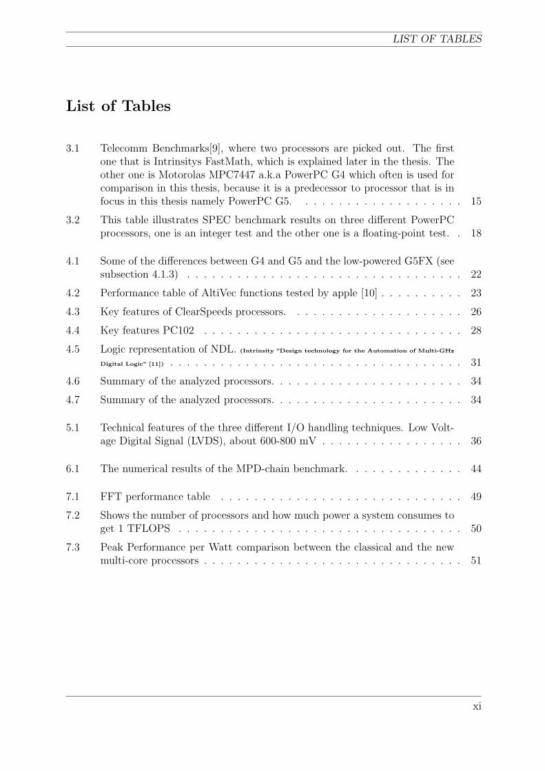
3.1 Telecomm Benchmarks[9], where two processors are picked out. The firstone that is Intrinsitys FastMath, which is explained later in the thesis. Theother one is Motorolas MPC7447 a.k.a PowerPC G4 which often is used forcomparison in this thesis, because it is a predecessor to processor that is infocus in this thesis namely PowerPC G5. . . . . . . . . . . . . . . . . . . . 15
3.2 This table illustrates SPEC benchmark results on three different PowerPCprocessors, one is an integer test and the other one is a floating-point test. . 18
4.1 Some of the differences between G4 and G5 and the low-powered G5FX (seesubsection 4.1.3) . . . . . . . . . . . . . . . . . . . . . . . . . . . . . . . . . 22
4.2 Performance table of AltiVec functions tested by apple [10] . . . . . . . . . . 23
4.3 Key features of ClearSpeeds processors. . . . . . . . . . . . . . . . . . . . . 26
4.4 Key features PC102 . . . . . . . . . . . . . . . . . . . . . . . . . . . . . . . 28
4.5 Logic representation of NDL. (Intrinsity ”Design technology for the Automation of Multi-GHz
Digital Logic” [11]) . . . . . . . . . . . . . . . . . . . . . . . . . . . . . . . . . . . 31
4.6 Summary of the analyzed processors. . . . . . . . . . . . . . . . . . . . . . . 34
4.7 Summary of the analyzed processors. . . . . . . . . . . . . . . . . . . . . . . 34
5.1 Technical features of the three different I/O handling techniques. Low Volt-age Digital Signal (LVDS), about 600-800 mV . . . . . . . . . . . . . . . . . 36
6.1 The numerical results of the MPD-chain benchmark. . . . . . . . . . . . . . 44
7.1 FFT performance table . . . . . . . . . . . . . . . . . . . . . . . . . . . . . 49
7.2 Shows the number of processors and how much power a system consumes toget 1 TFLOPS . . . . . . . . . . . . . . . . . . . . . . . . . . . . . . . . . . 50
7.3 Peak Performance per Watt comparison between the classical and the newmulti-core processors . . . . . . . . . . . . . . . . . . . . . . . . . . . . . . . 51
xi

EXTREME PROCESSORS FOR EXTREME PROCESSING
xii
CONTENTS
Contents
Preface iii
Abstract v
Abbreviations vii
1 Introduction 1
1.1 Future radar technology . . . . . . . . . . . . . . . . . . . . . . . . . . . . 1
1.1.1 Synthetic Aperture Radar . . . . . . . . . . . . . . . . . . . . . . . 2
1.2 Problem definition . . . . . . . . . . . . . . . . . . . . . . . . . . . . . . . 2
1.2.1 Survey . . . . . . . . . . . . . . . . . . . . . . . . . . . . . . . . . . 2
1.2.2 Multi-chip systems . . . . . . . . . . . . . . . . . . . . . . . . . . . 2
1.2.3 Implementation . . . . . . . . . . . . . . . . . . . . . . . . . . . . . 2
1.3 Related Work . . . . . . . . . . . . . . . . . . . . . . . . . . . . . . . . . . 3
1.3.1 Research and Development . . . . . . . . . . . . . . . . . . . . . . . 3
1.3.2 Previous work . . . . . . . . . . . . . . . . . . . . . . . . . . . . . . 3
2 Processor architecture 5
2.1 RISC . . . . . . . . . . . . . . . . . . . . . . . . . . . . . . . . . . . . . . . 6
2.2 CISC . . . . . . . . . . . . . . . . . . . . . . . . . . . . . . . . . . . . . . . 6
2.3 Superscalar . . . . . . . . . . . . . . . . . . . . . . . . . . . . . . . . . . . 7
2.4 VLIW . . . . . . . . . . . . . . . . . . . . . . . . . . . . . . . . . . . . . . 7
2.5 Multiprocessor . . . . . . . . . . . . . . . . . . . . . . . . . . . . . . . . . 8
2.6 Interconnection Networks . . . . . . . . . . . . . . . . . . . . . . . . . . . . 8
3 Theory 11
3.1 Fast Fourier Transform . . . . . . . . . . . . . . . . . . . . . . . . . . . . . 11
3.2 Medium Pulse repetition frequency Doppler radar chain . . . . . . . . . . . 12
3.3 Benchmarks . . . . . . . . . . . . . . . . . . . . . . . . . . . . . . . . . . . 14
3.3.1 The Embedded Microprocessor Benchmark Consortium . . . . . . . 15
3.3.2 Fastest Fourier Transform in the West . . . . . . . . . . . . . . . . 15
3.3.3 SPEC . . . . . . . . . . . . . . . . . . . . . . . . . . . . . . . . . . 18
xiii
EXTREME PROCESSORS FOR EXTREME PROCESSING
4 Processor survey 19
4.1 IBM . . . . . . . . . . . . . . . . . . . . . . . . . . . . . . . . . . . . . . . 19
4.1.1 POWER architecture . . . . . . . . . . . . . . . . . . . . . . . . . . 20
4.1.2 G4 vs. G5 . . . . . . . . . . . . . . . . . . . . . . . . . . . . . . . . 21
4.1.3 PowerPC 970FX . . . . . . . . . . . . . . . . . . . . . . . . . . . . 22
4.1.4 AltiVec . . . . . . . . . . . . . . . . . . . . . . . . . . . . . . . . . 22
4.1.5 Summary of the PowerPC 970 . . . . . . . . . . . . . . . . . . . . . 23
4.1.6 Key features of PowerPC 970 . . . . . . . . . . . . . . . . . . . . . 24
4.2 ClearSpeed . . . . . . . . . . . . . . . . . . . . . . . . . . . . . . . . . . . 24
4.2.1 CS301 . . . . . . . . . . . . . . . . . . . . . . . . . . . . . . . . . . 24
4.2.2 CSX600 . . . . . . . . . . . . . . . . . . . . . . . . . . . . . . . . . 25
4.2.3 Summary of ClearSpeeds processors . . . . . . . . . . . . . . . . . . 26
4.2.4 Key features of CS 301 and the CSX600 . . . . . . . . . . . . . . . 26
4.3 PicoChip . . . . . . . . . . . . . . . . . . . . . . . . . . . . . . . . . . . . . 27
4.3.1 Summary of PC 102 . . . . . . . . . . . . . . . . . . . . . . . . . . 28
4.3.2 Key features of PC 102 . . . . . . . . . . . . . . . . . . . . . . . . . 29
4.4 Intrinsity . . . . . . . . . . . . . . . . . . . . . . . . . . . . . . . . . . . . . 29
4.4.1 1-of-N Dynamic Logic . . . . . . . . . . . . . . . . . . . . . . . . . 30
4.4.2 Summary of FastMath . . . . . . . . . . . . . . . . . . . . . . . . . 31
4.4.3 Key features of FastMATH . . . . . . . . . . . . . . . . . . . . . . . 31
4.5 PACT . . . . . . . . . . . . . . . . . . . . . . . . . . . . . . . . . . . . . . 31
4.5.1 XPP architechture . . . . . . . . . . . . . . . . . . . . . . . . . . . 32
4.5.2 Summary of PACT processors . . . . . . . . . . . . . . . . . . . . . 33
4.5.3 Key features of XPP64-A . . . . . . . . . . . . . . . . . . . . . . . 33
4.6 Summary . . . . . . . . . . . . . . . . . . . . . . . . . . . . . . . . . . . . 34
5 Interconnection networks for multi-chip systems 35
5.1 Interconnection networks . . . . . . . . . . . . . . . . . . . . . . . . . . . . 35
5.1.1 3GIO . . . . . . . . . . . . . . . . . . . . . . . . . . . . . . . . . . . 35
5.1.2 RapidIO . . . . . . . . . . . . . . . . . . . . . . . . . . . . . . . . . 35
5.1.3 HyperTransport . . . . . . . . . . . . . . . . . . . . . . . . . . . . . 36
5.1.4 Summary . . . . . . . . . . . . . . . . . . . . . . . . . . . . . . . . 36
xiv
CONTENTS
6 Implementation 39
6.1 FFT implementation . . . . . . . . . . . . . . . . . . . . . . . . . . . . . . 39
6.1.1 Result of FFTW3 implementation . . . . . . . . . . . . . . . . . . . 39
6.1.2 Result of FFT implementation with AltiVec . . . . . . . . . . . . . 41
6.1.3 Summary of FFT implementation . . . . . . . . . . . . . . . . . . . 41
6.2 MPD-chain implementation . . . . . . . . . . . . . . . . . . . . . . . . . . 43
6.2.1 Result of MPD-chain implementation . . . . . . . . . . . . . . . . . 44
6.2.2 Summary of the MPD-chain benchmark . . . . . . . . . . . . . . . 45
7 Conclusion 47
7.1 Future architecture . . . . . . . . . . . . . . . . . . . . . . . . . . . . . . . 50
7.1.1 Technical aspects . . . . . . . . . . . . . . . . . . . . . . . . . . . . 50
7.1.2 Market aspect . . . . . . . . . . . . . . . . . . . . . . . . . . . . . . 52
7.2 Future Work . . . . . . . . . . . . . . . . . . . . . . . . . . . . . . . . . . . 52
Bibliography 55
A Result of FFTW3 implementation in table form 59
B Benchmark main.c 61
xv

EXTREME PROCESSORS FOR EXTREME PROCESSING
xvi
CHAPTER 1. INTRODUCTION
1 Introduction
The project Extreme Processors for Extreme Processing addresses a global problem in themodern world. Which is the desire to be able to compute larger amounts of data in lessertime. In this project the target is future airborne radar technology that is developed byEricsson Microwave Systems AB (EMW).
More specifically the project´s question is, if it is possible to use modern commercialprocessors, or have the demands grown beyond their capabilities?
EMW with its long experience in radar technology has been successful in developingairborne radar systems. One of their most successful radars was developed in the early1970s. This radar was later on used in JA 37 Viggen. In the 1990s this radar was regardedas the best airborne radar in Europe. The experiences from both the development of theradar PS46 and the research in wave propagation and antenna construction are importantcontributory factors for finding a good solution for future radar systems [12].
1.1 Future radar technology
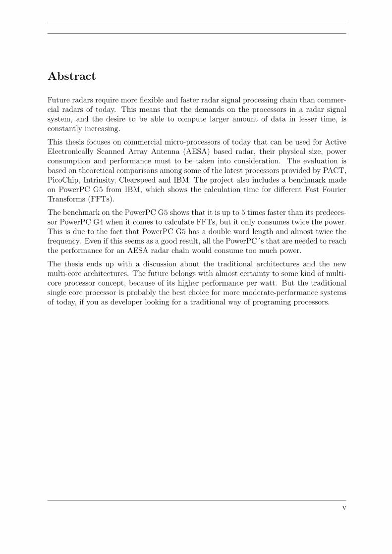
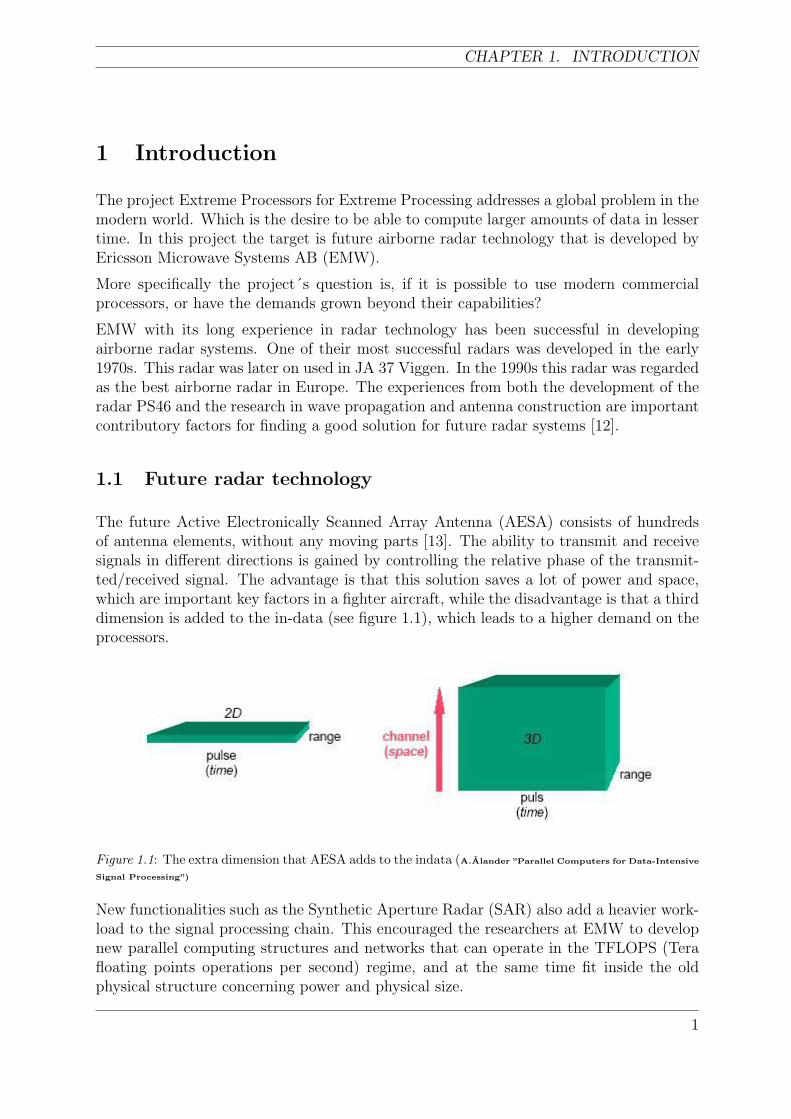
The future Active Electronically Scanned Array Antenna (AESA) consists of hundredsof antenna elements, without any moving parts [13]. The ability to transmit and receivesignals in different directions is gained by controlling the relative phase of the transmit-ted/received signal. The advantage is that this solution saves a lot of power and space,which are important key factors in a fighter aircraft, while the disadvantage is that a thirddimension is added to the in-data (see figure 1.1), which leads to a higher demand on theprocessors.
Figure 1.1: The extra dimension that AESA adds to the indata (A.Alander ”Parallel Computers for Data-Intensive
Signal Processing”)
New functionalities such as the Synthetic Aperture Radar (SAR) also add a heavier work-load to the signal processing chain. This encouraged the researchers at EMW to developnew parallel computing structures and networks that can operate in the TFLOPS (Terafloating points operations per second) regime, and at the same time fit inside the oldphysical structure concerning power and physical size.
1
EXTREME PROCESSORS FOR EXTREME PROCESSING
1.1.1 Synthetic Aperture Radar
Synthetic Aperture Radar (SAR) is a way to electronically manufacture a ground pictureusing radar technology. The benefit of using this technology instead of cameras is that itis independent of the weather. The result will be the same even if it is cloudy, rainy ordark.
The technique is based on sampling ground echoes of a moving radar. The series of echoesare then combined by using large FFT calculations that creates a synthetic aperture whichis much larger than the length of the aircraft [14].
1.2 Problem definition
Future radar equipments such as the multi-mode AESA radar demands more flexible andfaster radar signal processing chain than commercial radars of today, but still fits insidethe old ”box” in terms of physical size and power consumptions. This means that thefuture processing nodes must be capable of handling not only larger volumes of data butalso the changing size of the in-data in contrast to the one mode radar of today which hasa fixed size of in-data. The processing nodes will be limited to commercial processors.
To be able to solve this task, the project will be divided into three main areas:
• Make a survey over the most interesting processors.
• Make studies of multi-chip systems for radar signal processing.
• Make implementation studies of radar algorithms on a processor.
1.2.1 Survey
The market is a swarm of different processors and architectures and of course are notall meant for radar processing chains. The first task for the project is to find interestingprocessors and architectures that could work as backbone in future radar equipments.
1.2.2 Multi-chip systems
It is clear that no processor in a near future is capable to singly performing in the TFLOPSregime, the future radar processing systems must also be based on some sort of multi-chipsystems. In this area, the work will focus on the bottle neck of I/O handling and naturallythe focus will be on systems consisting of processors examined in this thesis.
1.2.3 Implementation
As the processors and architectures performance increase, their complexity will increaseas well; this means it puts more demands on the programmer and software for maximumperformance. This will be studied by making an implementation of a radar algorithm ona chosen processor; whose performance and engineering efficiency will be measured andevaluated.
2
CHAPTER 1. INTRODUCTION
1.3 Related Work
This thesis is conducted in cooperation between three master theses groups, EMW andCenter for Research on Embedded Systems (CERES) at Halmstad University. One of thegroups (R. Karlsson and B. Byline [15]) has also studied micro-processors, but concentrateon more highly parallel architectures. The other group (Z. Ul-Abdin, O. Johnsson M.Stenemo [16])examines streaming languages for parallel architectures. The overall goal ofthis research is to find interesting architectures/processors for future radar equipment.
1.3.1 Research and Development
At the National Defense Research Establishment of Sweden in 1996 L. Pettersson et.albuilt an experimental S-band antenna that performs digital beam forming [17]. Theydemonstrated the experiment by using a special designed ASIC as processing element [18]but failed to run it at real time which is a demand in the area of airborne radar. The goalof the future was to obtain the result in real time. These results were quite similar all overthe world at that time, where we had the radar technology but no processing elements thatcould handle the data it created. Since then there has been numerous attempts to solvethis problem. For example a research project is conducted at MIT Lincoln Laboratory,where researchers are building a signal processor for an airborne radar system that issupposed to operate at a speed of one trillion operations per second [19]. This can besummarized that until resent years no commercial processor has been, suitable for thenew kind of airborne radars.
In an article in Military & Aerospace Electronics [20], John Keller is addressing radarprocessing which shifts from Digital Signal Processors (DSP) to Field ProgrammableGate Arrays (FPGA) and SIMD structures such as AltiVec. He refers to many leadingcompanies in radar technology and processor companies states that they all agree that forfuture signal processing chains in radar technology DSP solutions are history,and assertsthat more general-purpose chips such as AltiVec and FPGA solutions are the future.
There is a lot of money spend on these questions; one example is in United States wherethe US Air Force is spending $888 million dollar to Northrop Grumman Corporation for aresearch project that is supposed to develop, integrate and test the Multi-Platform RadarTechnology Insertion Program (MP-RTIP)[21].
1.3.2 Previous work
One of the earlier EMW projects in the area was entitled ”High-Speed Signal Processing”(HSSP). A report by Anders Ahlander and Per Soderstam [13] summarized the project.It addressed the signal processing demands and a solution for the AESA system. The so-lution was based on technology in late 1990s. At that time no commercial micro processorwas powerful enough to be used as a computing node in the system. They proposed a sys-tem based on computing nodes built with Application Specific Integrated Circuit (ASIC)technology available in 2001. The desired system design is a high-level Multiple Instruc-tion stream, Multiple Data stream (MIMD) system using a high-speed time-deterministic
3
EXTREME PROCESSORS FOR EXTREME PROCESSING
intermodule communication network. The modules are moderately parallel Single Instruc-tion stream, Multiple Data stream (SIMD) processor arrays based on pipelined floatingpoint processors [13].
There is also a recent master project performed on the same topic at Halmstad University,one of them was presented by F Gunnarson and C Hansson in 2002. They examined theefficiency of the two parallel architecture BOPS 2x2 ManArray and the PACT XPU128[22].
4
CHAPTER 2. PROCESSOR ARCHITECTURE
2 Processor architecture
Ever since the birth of the first computer, the demands have grown at a steady rate whichhave forced the developers to create newer and faster computers to keep up with thedemands.
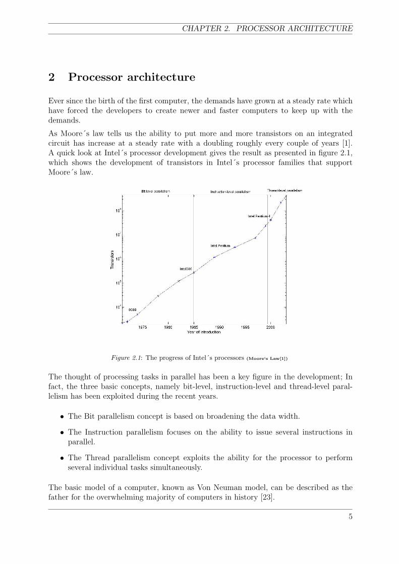
As Moore´s law tells us the ability to put more and more transistors on an integratedcircuit has increase at a steady rate with a doubling roughly every couple of years [1].A quick look at Intel´s processor development gives the result as presented in figure 2.1,which shows the development of transistors in Intel´s processor families that supportMoore´s law.
Figure 2.1: The progress of Intel´s processors (Moore‘s Law[1])
The thought of processing tasks in parallel has been a key figure in the development; Infact, the three basic concepts, namely bit-level, instruction-level and thread-level paral-lelism has been exploited during the recent years.
• The Bit parallelism concept is based on broadening the data width.
• The Instruction parallelism focuses on the ability to issue several instructions inparallel.
• The Thread parallelism concept exploits the ability for the processor to performseveral individual tasks simultaneously.
The basic model of a computer, known as Von Neuman model, can be described as thefather for the overwhelming majority of computers in history [23].
5
EXTREME PROCESSORS FOR EXTREME PROCESSING
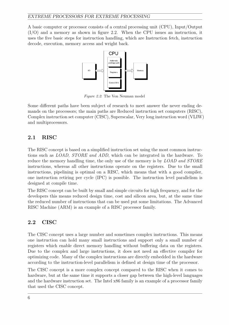
A basic computer or processor consists of a central processing unit (CPU), Input/Output(I/O) and a memory as shown in figure 2.2. When the CPU issues an instruction, ituses the five basic steps for instruction handling, which are Instruction fetch, instructiondecode, execution, memory access and wright back.
Figure 2.2: The Von Neuman model
Some different paths have been subject of research to meet answer the never ending de-mands on the processors; the main paths are Reduced instruction set computers (RISC),Complex instruction set computer (CISC), Superscalar, Very long instruction word (VLIW)and multiprocessors.
2.1 RISC
The RISC concept is based on a simplified instruction set using the most common instruc-tions such as LOAD, STORE and ADD, which can be integrated in the hardware. Toreduce the memory handling time, the only use of the memory is by LOAD and STOREinstructions, whereas all other instructions operate on the registers. Due to the smallinstructions, pipelining is optimal on a RISC, which means that with a good compiler,one instruction retiring per cycle (IPC) is possible. The instruction level parallelism isdesigned at compile time.
The RISC concept can be built by small and simple circuits for high frequency, and for thedevelopers this means reduced design time, cost and silicon area, but, at the same timethe reduced number of instructions that can be used put some limitations. The AdvancedRISC Machine (ARM) is an example of a RISC processor family.
2.2 CISC
The CISC concept uses a large number and sometimes complex instructions. This meansone instruction can hold many small instructions and support only a small number ofregisters which enable direct memory handling without buffering data on the registers.Due to the complex and large instructions, it does not need an effective compiler foroptimizing code. Many of the complex instructions are directly embedded in the hardwareaccording to the instruction-level parallelism is defined at design time of the processor.
The CISC concept is a more complex concept compared to the RISC when it comes tohardware, but at the same time it supports a closer gap between the high-level languagesand the hardware instruction set. The Intel x86 family is an example of a processor familythat used the CISC concept.
6
CHAPTER 2. PROCESSOR ARCHITECTURE
2.3 Superscalar
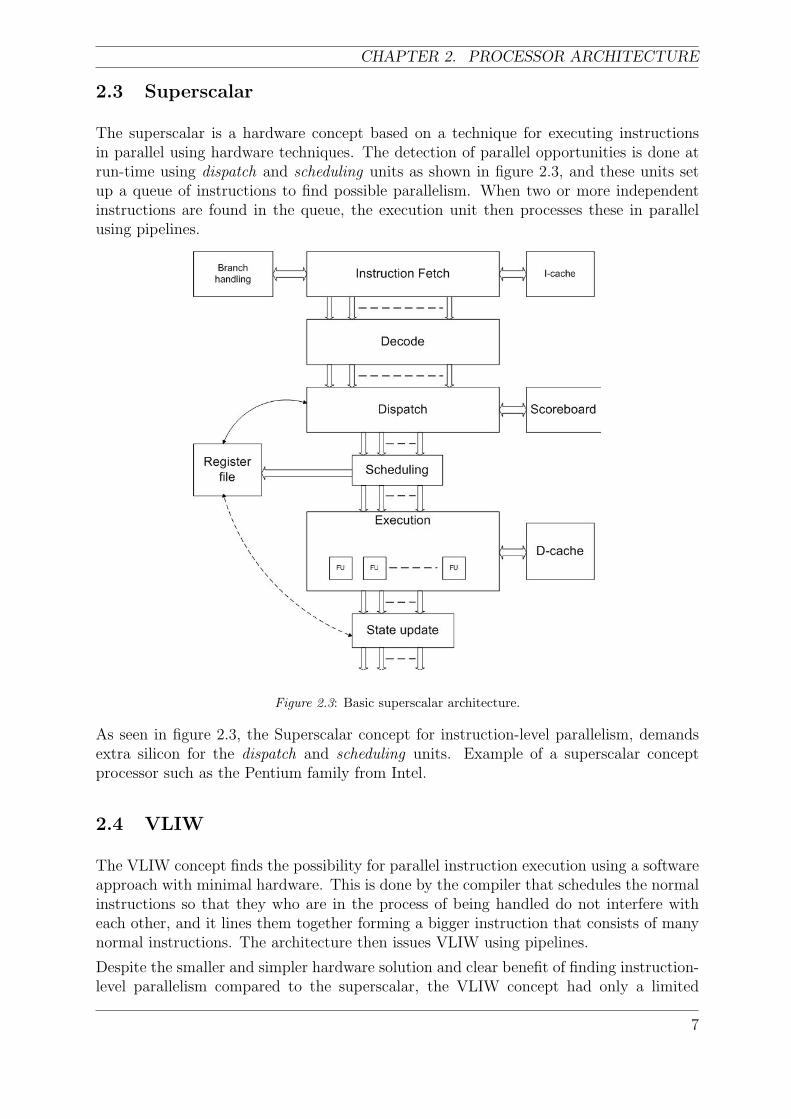
The superscalar is a hardware concept based on a technique for executing instructionsin parallel using hardware techniques. The detection of parallel opportunities is done atrun-time using dispatch and scheduling units as shown in figure 2.3, and these units setup a queue of instructions to find possible parallelism. When two or more independentinstructions are found in the queue, the execution unit then processes these in parallelusing pipelines.
Figure 2.3: Basic superscalar architecture.
As seen in figure 2.3, the Superscalar concept for instruction-level parallelism, demandsextra silicon for the dispatch and scheduling units. Example of a superscalar conceptprocessor such as the Pentium family from Intel.
2.4 VLIW
The VLIW concept finds the possibility for parallel instruction execution using a softwareapproach with minimal hardware. This is done by the compiler that schedules the normalinstructions so that they who are in the process of being handled do not interfere witheach other, and it lines them together forming a bigger instruction that consists of manynormal instructions. The architecture then issues VLIW using pipelines.
Despite the smaller and simpler hardware solution and clear benefit of finding instruction-level parallelism compared to the superscalar, the VLIW concept had only a limited
7
EXTREME PROCESSORS FOR EXTREME PROCESSING
success at the commercial market, but in the last few years some commercial processorshave emerged mainly in the signal processor market, like the TMS320C6x family fromTexas Instruments.
2.5 Multiprocessor
During the last years, the development of processors based on Moore´s law has cometo a standstill mainly due to power issue, as it is simply not possible to cool down theprocessors of tomorrow [24]. This has opened the door for new families of processors usinga concept that puts several processing elements in the same silica, which enables the useof lower clock frequency for lesser power consumption.
The number of processing elements that are used can range from a couple to several hun-dreds which are reflected in their complexity, where some are almost full sized processorswhile others are only small arithmetical units.
2.6 Interconnection Networks
There are different parallel computation models but the two basic concepts are:
• Single Instruction stream, Multiple Data streams (SIMD)
• Multiple Instruction streams, Multiple Data streams (MIMD)
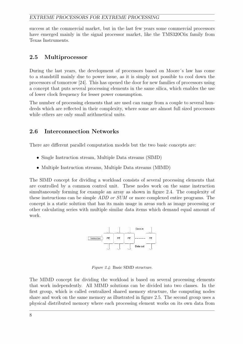
The SIMD concept for dividing a workload consists of several processing elements thatare controlled by a common control unit. These nodes work on the same instructionsimultaneously forming for example an array as shown in figure 2.4. The complexity ofthese instructions can be simple ADD or SUM or more complexed entire programs. Theconcept is a static solution that has its main usage in areas such as image processing orother calculating series with multiple similar data items which demand equal amount ofwork.
Figure 2.4: Basic SIMD structure.
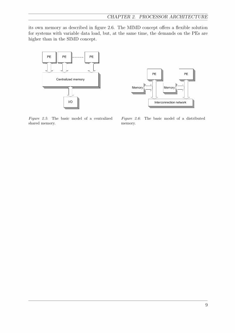
The MIMD concept for dividing the workload is based on several processing elementsthat work independently. All MIMD solutions can be divided into two classes. In thefirst group, which is called centralized shared memory structure, the computing nodesshare and work on the same memory as illustrated in figure 2.5. The second group uses aphysical distributed memory where each processing element works on its own data from
8
CHAPTER 2. PROCESSOR ARCHITECTURE
its own memory as described in figure 2.6. The MIMD concept offers a flexible solutionfor systems with variable data load, but, at the same time, the demands on the PEs arehigher than in the SIMD concept.
Figure 2.5: The basic model of a centralizedshared memory.
Figure 2.6: The basic model of a distributedmemory.
9

EXTREME PROCESSORS FOR EXTREME PROCESSING
10
CHAPTER 3. THEORY
3 Theory
This chapter will cover theory that is needed to understand some of the problems andchallenges that this project encounters. First an introduction to Fast Fourier Transform(FFT) is presented in section 3.1, and section 3.2 examines the Medium Pulse repetitionfrequency Doppler -radar chain (MPD-chain). Whereas section 3.3 tackles some differentbenchmark companies and techniques that are of interest.
3.1 Fast Fourier Transform
Discrete Fourier Transform (DFT) is a mathematical technique used for analyzing periodicdigital series of observations: x(t) = 0, ...., N − 1 where N is typically a large number.DFTs main applications are in image processing, communication and radar.
When analyzing digital series using DFT, the assumption is that there are periodicalrepeating patterns hidden in the series of observations and also other phenomena that arenot repeated in any discernible cyclic way, often called ”noise”. The DFT helps to identifythe cyclic phenomena [25].
The mathematic definition of a DFT is displayed in equation 3.1
XN [k] =N−1∑n=0
x[n]e−j( 2πN
)kn k = 0, . . . N − 1 (3.1)
The size of N in a DFT is often a factor of power of two like 128, 256, 512 and so on.
There are different ways to implement and calculate a DFT based on equation 3.1 onto aprocessor. The two basic ideas are [26]:
First, the ”hard”way, which is simply to add together the sum of all N using equation 3.1.This means that for N different k values demand N2 multiplications, and to sum up allN values, each k will take N(N − 1) additions. Totally 2N2 − N ≈ 2N2 arithmeticoperations. When using DSP, the time it takes to sum is neglected compared to the timeit takes to multiply. Therefor, the time it takes to calculate large N can be approximatedto equation 3.2 [26]:
CalculationT ime = 2N2 ≈ N2 (3.2)
The second method is by using an FFT algorithm. An FFT algorithm, which is basedon equation 3.1 uses another way to calculate it other than the ”hard” way. It divides aDFT with N points into N DFTs. First divide a N equation 3.1 into two N/2 equationsas shown in equation 3.3 where the equation is divided into a sum of all even numbers(n = 2a) and one sum of all uneven (n = 2a + 1) [26].
11
EXTREME PROCESSORS FOR EXTREME PROCESSING
XN [k] =
N/2−1∑a=0
x[2a]e−j( 2πN
)k2a +
N/2−1∑a=0
x[2a + 1]e−j( 2πN
)k(2a+1) (3.3)
Equation 3.3 can then be divided into two N/4s and so on until N DFTs are created.How long time should it take to calculate a DFT by using a FFT algorithm?
Since the size of N is a factor of two, one can say that N = 2A where A is an even integer.The dividing of equation 3.1 continues down to A = log N steps. For each step in the FFTalgorithm, N multiplications and as many additions are needed, since there are totallylog N steps the total will be 2N log N . When using a processor, the multiplication takesa much longer time than the additions which give the calculation time 3.4.
CalculationT ime = N log N (3.4)
When comparing the two calculation time´s equatios 3.2 and 3.4, one can easily see thebenefit of using an FFT algorithm.
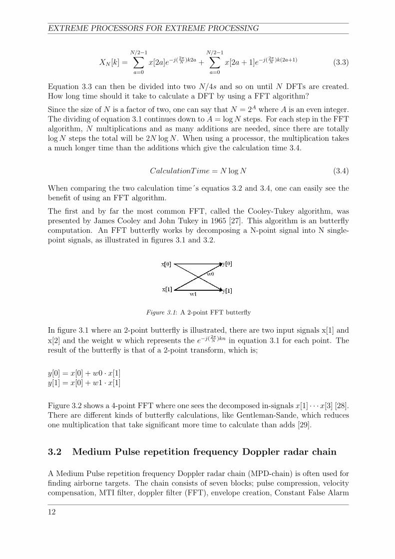
The first and by far the most common FFT, called the Cooley-Tukey algorithm, waspresented by James Cooley and John Tukey in 1965 [27]. This algorithm is an butterflycomputation. An FFT butterfly works by decomposing a N-point signal into N single-point signals, as illustrated in figures 3.1 and 3.2.
Figure 3.1: A 2-point FFT butterfly
In figure 3.1 where an 2-point butterfly is illustrated, there are two input signals x[1] and
x[2] and the weight w which represents the e−j( 2πN
)kn in equation 3.1 for each point. Theresult of the butterfly is that of a 2-point transform, which is;
y[0] = x[0] + w0 · x[1]y[1] = x[0] + w1 · x[1]
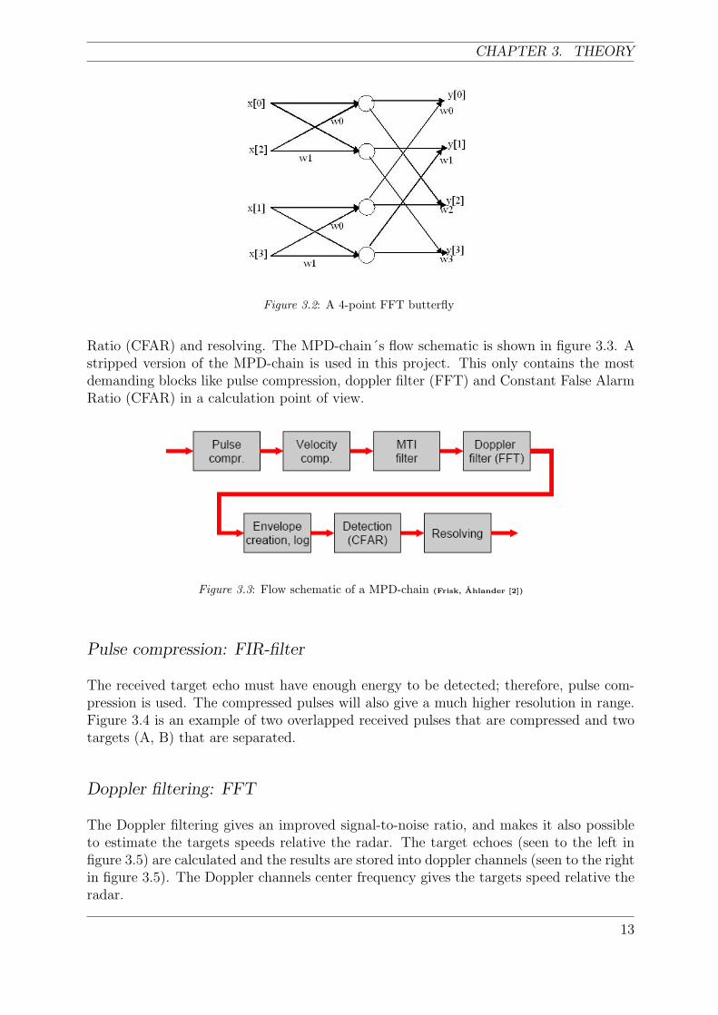
Figure 3.2 shows a 4-point FFT where one sees the decomposed in-signals x[1] · · ·x[3] [28].There are different kinds of butterfly calculations, like Gentleman-Sande, which reducesone multiplication that take significant more time to calculate than adds [29].
3.2 Medium Pulse repetition frequency Doppler radar chain
A Medium Pulse repetition frequency Doppler radar chain (MPD-chain) is often used forfinding airborne targets. The chain consists of seven blocks; pulse compression, velocitycompensation, MTI filter, doppler filter (FFT), envelope creation, Constant False Alarm
12
CHAPTER 3. THEORY
Figure 3.2: A 4-point FFT butterfly
Ratio (CFAR) and resolving. The MPD-chain´s flow schematic is shown in figure 3.3. Astripped version of the MPD-chain is used in this project. This only contains the mostdemanding blocks like pulse compression, doppler filter (FFT) and Constant False AlarmRatio (CFAR) in a calculation point of view.
Figure 3.3: Flow schematic of a MPD-chain (Frisk, Ahlander [2])
Pulse compression: FIR-filter
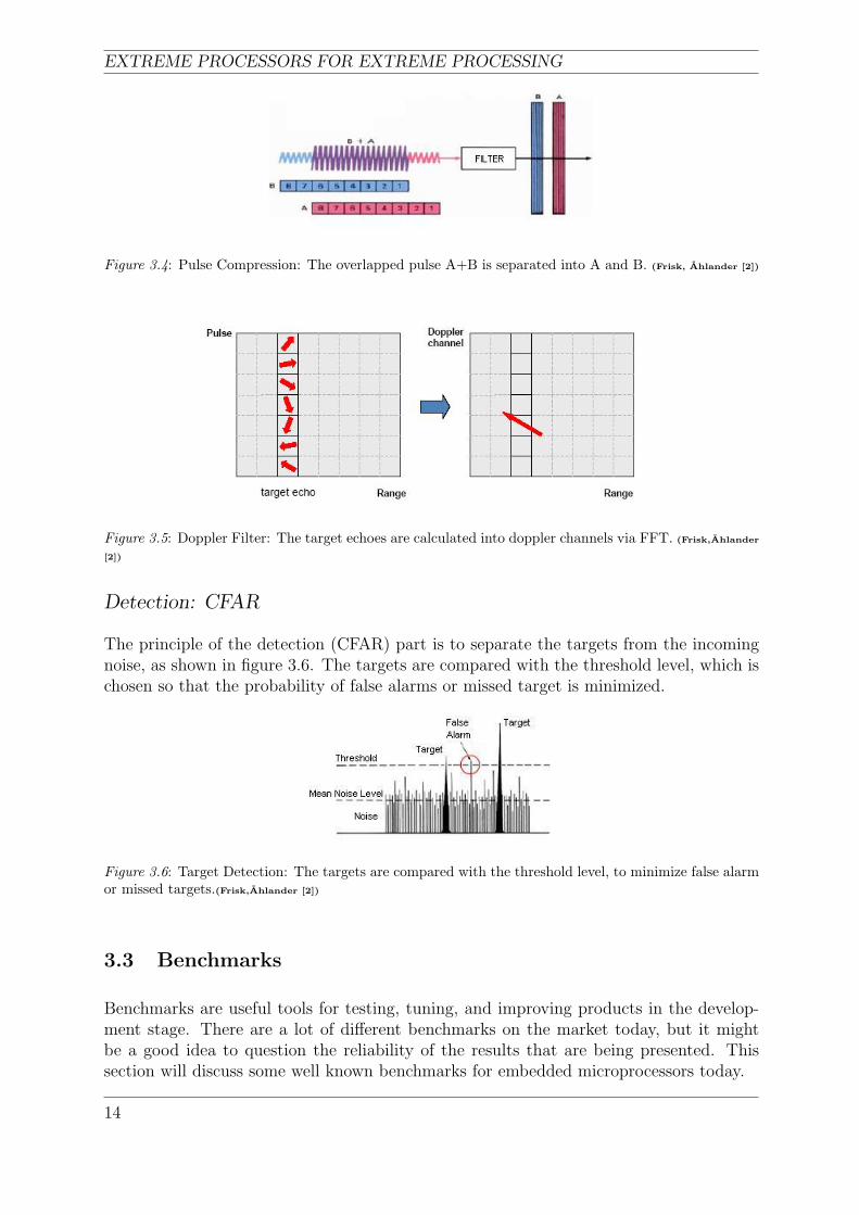
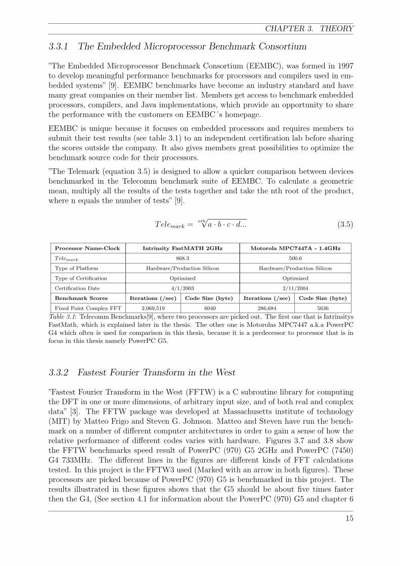
The received target echo must have enough energy to be detected; therefore, pulse com-pression is used. The compressed pulses will also give a much higher resolution in range.Figure 3.4 is an example of two overlapped received pulses that are compressed and twotargets (A, B) that are separated.
Doppler filtering: FFT
The Doppler filtering gives an improved signal-to-noise ratio, and makes it also possibleto estimate the targets speeds relative the radar. The target echoes (seen to the left infigure 3.5) are calculated and the results are stored into doppler channels (seen to the rightin figure 3.5). The Doppler channels center frequency gives the targets speed relative theradar.
13
EXTREME PROCESSORS FOR EXTREME PROCESSING
Figure 3.4: Pulse Compression: The overlapped pulse A+B is separated into A and B. (Frisk, Ahlander [2])
Figure 3.5: Doppler Filter: The target echoes are calculated into doppler channels via FFT. (Frisk,Ahlander
[2])
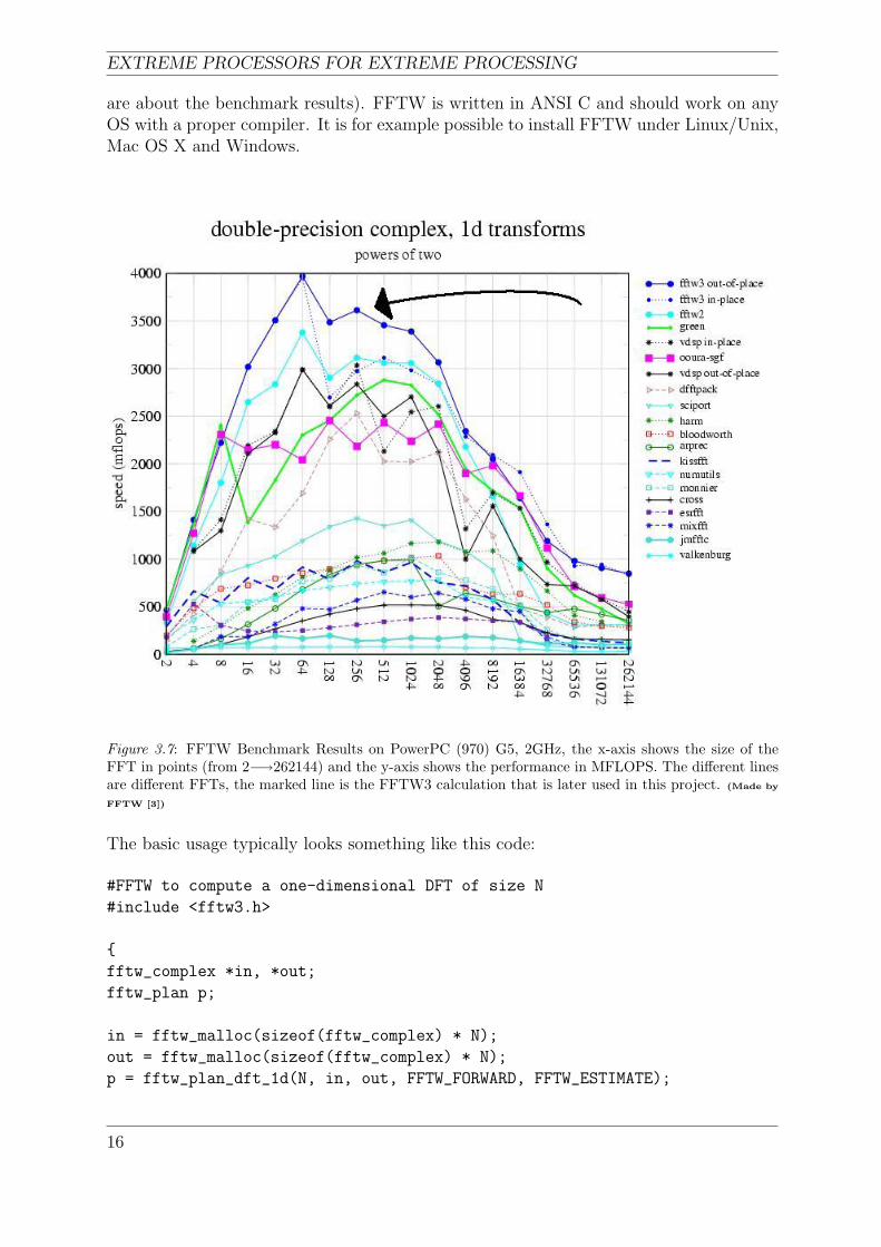
Detection: CFAR
The principle of the detection (CFAR) part is to separate the targets from the incomingnoise, as shown in figure 3.6. The targets are compared with the threshold level, which ischosen so that the probability of false alarms or missed target is minimized.
Figure 3.6: Target Detection: The targets are compared with the threshold level, to minimize false alarmor missed targets.(Frisk,Ahlander [2])
3.3 Benchmarks
Benchmarks are useful tools for testing, tuning, and improving products in the develop-ment stage. There are a lot of different benchmarks on the market today, but it mightbe a good idea to question the reliability of the results that are being presented. Thissection will discuss some well known benchmarks for embedded microprocessors today.
14
CHAPTER 3. THEORY
3.3.1 The Embedded Microprocessor Benchmark Consortium
”The Embedded Microprocessor Benchmark Consortium (EEMBC), was formed in 1997to develop meaningful performance benchmarks for processors and compilers used in em-bedded systems” [9]. EEMBC benchmarks have become an industry standard and havemany great companies on their member list. Members get access to benchmark embeddedprocessors, compilers, and Java implementations, which provide an opportunity to sharethe performance with the customers on EEMBC´s homepage.
EEMBC is unique because it focuses on embedded processors and requires members tosubmit their test results (see table 3.1) to an independent certification lab before sharingthe scores outside the company. It also gives members great possibilities to optimize thebenchmark source code for their processors.
”The Telemark (equation 3.5) is designed to allow a quicker comparison between devicesbenchmarked in the Telecomm benchmark suite of EEMBC. To calculate a geometricmean, multiply all the results of the tests together and take the nth root of the product,where n equals the number of tests” [9].
Telemark =nth√
a · b · c · d... (3.5)
Processor Name-Clock Intrinsity FastMATH 2GHz Motorola MPC7447A - 1.4GHz
Telemark 868.3 500.6
Type of Platform Hardware/Production Silicon Hardware/Production Silicon
Type of Certification Optimized Optimized
Certification Date 4/1/2003 2/11/2004
Benchmark Scores Iterations (/sec) Code Size (byte) Iterations (/sec) Code Size (byte)
Fixed Point Complex FFT 2,069,519 6040 286,684 5636
Table 3.1: Telecomm Benchmarks[9], where two processors are picked out. The first one that is IntrinsitysFastMath, which is explained later in the thesis. The other one is Motorolas MPC7447 a.k.a PowerPCG4 which often is used for comparison in this thesis, because it is a predecessor to processor that is infocus in this thesis namely PowerPC G5.
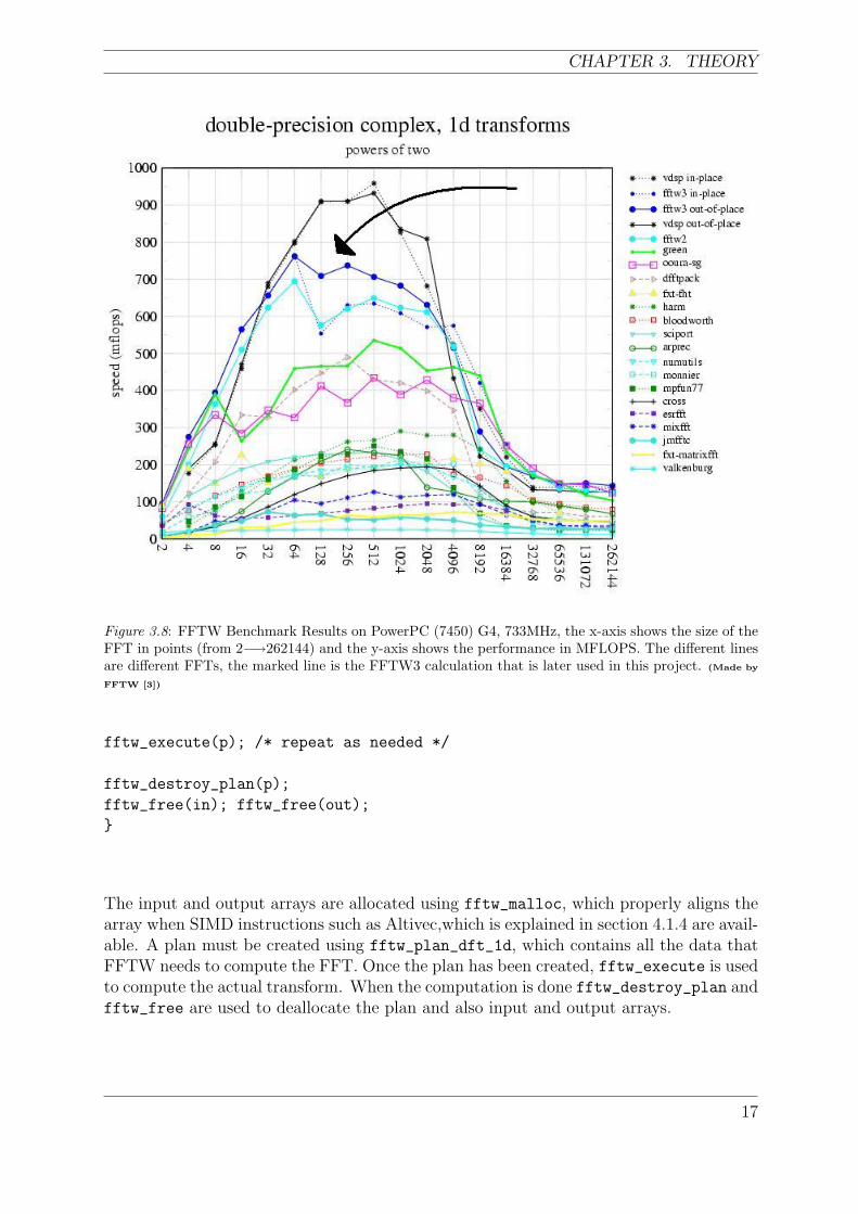
3.3.2 Fastest Fourier Transform in the West
”Fastest Fourier Transform in the West (FFTW) is a C subroutine library for computingthe DFT in one or more dimensions, of arbitrary input size, and of both real and complexdata” [3]. The FFTW package was developed at Massachusetts institute of technology(MIT) by Matteo Frigo and Steven G. Johnson. Matteo and Steven have run the bench-mark on a number of different computer architectures in order to gain a sense of how therelative performance of different codes varies with hardware. Figures 3.7 and 3.8 showthe FFTW benchmarks speed result of PowerPC (970) G5 2GHz and PowerPC (7450)G4 733MHz. The different lines in the figures are different kinds of FFT calculationstested. In this project is the FFTW3 used (Marked with an arrow in both figures). Theseprocessors are picked because of PowerPC (970) G5 is benchmarked in this project. Theresults illustrated in these figures shows that the G5 should be about five times fasterthen the G4, (See section 4.1 for information about the PowerPC (970) G5 and chapter 6
15
EXTREME PROCESSORS FOR EXTREME PROCESSING
are about the benchmark results). FFTW is written in ANSI C and should work on anyOS with a proper compiler. It is for example possible to install FFTW under Linux/Unix,Mac OS X and Windows.
Figure 3.7: FFTW Benchmark Results on PowerPC (970) G5, 2GHz, the x-axis shows the size of theFFT in points (from 2−→262144) and the y-axis shows the performance in MFLOPS. The different linesare different FFTs, the marked line is the FFTW3 calculation that is later used in this project. (Made by
FFTW [3])
The basic usage typically looks something like this code:
#FFTW to compute a one-dimensional DFT of size N
#include <fftw3.h>
{
fftw_complex *in, *out;
fftw_plan p;
in = fftw_malloc(sizeof(fftw_complex) * N);
out = fftw_malloc(sizeof(fftw_complex) * N);
p = fftw_plan_dft_1d(N, in, out, FFTW_FORWARD, FFTW_ESTIMATE);
16
CHAPTER 3. THEORY
Figure 3.8: FFTW Benchmark Results on PowerPC (7450) G4, 733MHz, the x-axis shows the size of theFFT in points (from 2−→262144) and the y-axis shows the performance in MFLOPS. The different linesare different FFTs, the marked line is the FFTW3 calculation that is later used in this project. (Made by
FFTW [3])
fftw_execute(p); /* repeat as needed */
fftw_destroy_plan(p);
fftw_free(in); fftw_free(out);
}
The input and output arrays are allocated using fftw_malloc, which properly aligns thearray when SIMD instructions such as Altivec,which is explained in section 4.1.4 are avail-able. A plan must be created using fftw_plan_dft_1d, which contains all the data thatFFTW needs to compute the FFT. Once the plan has been created, fftw_execute is usedto compute the actual transform. When the computation is done fftw_destroy_plan andfftw_free are used to deallocate the plan and also input and output arrays.
17
EXTREME PROCESSORS FOR EXTREME PROCESSING
3.3.3 SPEC
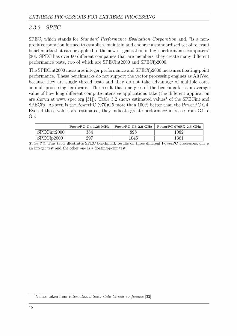
SPEC, which stands for Standard Performance Evaluation Corporation and, ”is a non-profit corporation formed to establish, maintain and endorse a standardized set of relevantbenchmarks that can be applied to the newest generation of high-performance computers”[30]. SPEC has over 60 different companies that are members, they create many differentperformance tests, two of which are SPECint2000 and SPECfp2000.
The SPECint2000 measures integer performance and SPECfp2000 measures floating-pointperformance. These benchmarks do not support the vector processing engines as AltiVec,because they are single thread tests and they do not take advantage of multiple coresor multiprocessing hardware. The result that one gets of the benchmark is an averagevalue of how long different compute-intensive applications take (the different applicationare shown at www.spec.org [31]). Table 3.2 shows estimated values1 of the SPECint andSPECfp. As seen is the PowerPC (970)G5 more than 100% better than the PowerPC G4.Even if these values are estimated, they indicate greate performace increase from G4 toG5.
PowerPC G4 1.25 MHz PowerPC G5 2.0 GHz PowerPC 970FX 2.5 GHz
SPECint2000 384 898 1082SPECfp2000 297 1045 1361
Table 3.2: This table illustrates SPEC benchmark results on three different PowerPC processors, one isan integer test and the other one is a floating-point test.
1Values taken from International Solid-state Circuit conference [32]
18
CHAPTER 4. PROCESSOR SURVEY
4 Processor survey
In this project, different processors are analyzed to see if they meet the requirements ofthe problem. The selected processors are divided into two categories. The first is theclassic architecture of fast processors, which consist of one processing unit with multiplefunctional units. This category often has a high clock frequency (typically > 1Ghz) andis able to use multiple threads. Among the processors that are studied in this thesis,the PowerPC 970 is the only one that belongs to this category. The other types ofprocessors are the ones that consist of several or more processing elements, which use alower frequency (typically 100-300Mhz) and thus gain power.
This chapter presents the processors that were useful and interesting to this project. Eachintroduction ends up with a table that contains some interesting performance features forthe processor. The performance of the figures will be introduced in giga instructions perseconds (GIPS), giga operations per second (GOPS) and giga floating point operationsper second (GFLOPS), because different manufacturers present different units.
4.1 IBM
The fifth generation of PowerPC called PowerPC 970 or PowerPC G5 is introduced byIBM. This is a 64-bit processor with a core based on the POWER4 architecture, (page 21in section 4.1.1) with a vector-processing engine called AltiVec (page 23 in section 4.1.4).The 64-bit solution has many significant advantages, such as the possibility of using morethan 4 GB ( 232 ≈ 4.3 · 109) of physical memory that ordinary 32-bit architecture canuse. Theoretically, it is possible to address up to 264 ≈ 18 · 1018B of memory. But the G5only uses 42-bit to address memory. Another advantage is that it takes less clock-cyclesto calculate large instructions [33]. This processor also has an additional floating-pointunit which gives it better performance because it eliminates some bottlenecks. There isalso has an additional load/store unit that allows more memory accesses to be processedper cycle, which together with a high bandwidth make the G5 capable of consuming a lotof data [34].
The PowerPC 970 family is designed to calculate 32-bit data at full speed with its 32-bitunidirectional bus, which means that data can always be sent in any direction. It alsohas the possibility to execute both at a 32-bit environment and mixed 32/64-bit and ofcourse 64-bit environment.
In figure 4.1 an overview of the functional blocks is provided for a better understandingof the 970 family.
• The first functional block is the L2 cache memory, which fetches data from theRAM memory to the execution core. Then the instruction is prefetched to the L1instruction cache and the L1 data cache can prefetch eight active data streams atthe same time.
19
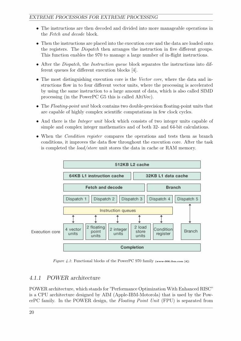
EXTREME PROCESSORS FOR EXTREME PROCESSING
• The instructions are then decoded and divided into more manageable operations inthe Fetch and decode block.
• Then the instructions are placed into the execution core and the data are loaded ontothe registers. The Dispatch then arranges the instruction in five different groups.This function enables the 970 to manage a large number of in-flight instructions.
• After the Dispatch, the Instruction queue block separates the instructions into dif-ferent queues for different execution blocks [4].
• The most distinguishing execution core is the Vector core, where the data and in-structions flow in to four different vector units, where the processing is acceleratedby using the same instruction to a large amount of data, which is also called SIMDprocessing (in the PowerPC G5 this is called AltiVec).
• The Floating-point unit block contains two double-precision floating-point units thatare capable of highly complex scientific computations in few clock cycles.
• And there is the Integer unit block which consists of two integer units capable ofsimple and complex integer mathematics and of both 32- and 64-bit calculations.
• When the Condition register compares the operations and tests them as branchconditions, it improves the data flow throughout the execution core. After the taskis completed the load/store unit stores the data in cache or RAM memory.
Figure 4.1: Functional blocks of the PowerPC 970 family (www-306.ibm.com [4])
4.1.1 POWER architecture
POWER architecture, which stands for ”Performance Optimization With Enhanced RISC”is a CPU architecture designed by AIM (Apple-IBM-Motorola) that is used by the Pow-erPC family. In the POWER design, the Floating Point Unit (FPU) is separated from
20
CHAPTER 4. PROCESSOR SURVEY
the instruction decoder and the integer parts, which allow the decoder to send instruc-tions to the FPU and the Arithmetical Logic Units (ALU) at the same time. A complexinstruction decoder is added to fetch one instruction, decode another and send one to theALU and CPU at the same time. The outcome of this is one of the first superscalar CPUdesigns. The POWER design is now at its fourth generation; the first POWER1 consistedof three chips (branch, integer, floating point) wired together on a board to create a sin-gle system. For generation two, another floating point unit, 256 kB cache and a 128-bitmath unit was added. The third generation POWER3 was the first to move into 64-bitarchitecture, where a third ALU and one more instruction decoder were added to a totalof eight functional units. Then came the POWER4, where four pairs of POWER3 CPUare added onto a motherboard, the frequency is increased and a high-speed connection isplaced between them. The POWER4 even in its single form is considered one of the mostpowerful CPUs on the market, but it consumes an astonishing 500 W [35].
4.1.2 G4 vs. G5
The main differences between PowerPC G4 and the PowerPC G5 will be examined in thissection.
• The main and most evident difference is the word length of 64-bit on the G5 com-pared with 32-bit on the G4.
• Another difference is the extremely wide execution core of the G5 which is able tohave over 200 instructions in flight, compared with 16 instructions on the G4 [36].
• The G5 has two floating point units and two load/store units compared with theG4 that has one of each.
• The G4 has four integers compared with two on the G5, but the G4´s integer unitsare three simple and one complex where the complex is the only one that can eithercalculate, multiply or divide. The G5´s two integers can both handle multiply andone of them can also divide.
• The G5´s pipelines have 23 stages compared with the G4 which has 7 , but thisresults in that the branch mis-predictions are more costly [34]. However, this issolved by adding branch prediction logic to the core, which solves this problem [36].
• The throughput separates the G5 from the G4. The G4 has a throughput of about800MByte/s, which means that most of the time the G4 is waiting for data. Wheresthe G5 has an EIO Elastic IO Front-Side bus which is two unidirectional 32-bitbuses with a bit rate of 8GByte/s.
• Table 4.11 shows various features on the G4 and G5.
The G4´s design is based on the philosophy called by Jon Stokes [36] as ”wide and shallow”.This means that the execution core executes a wide range of instructions at the same timebut the amount of instructions is small. The front can execute four instructions in one
1Data is taken from arstechnica.com/ [34] and www-306.ibm.com/ [4]
21
EXTREME PROCESSORS FOR EXTREME PROCESSING
PowerPC G4 G5 G5FXBits 32 64 64Clock speed [GHz] 0.55-1.42 1.6-2.0 2.0-2.5L2 Cache [kB] 256 512 512Bus speed [MHz] 167 800-1000 1100Latency [nSec] 95 135 119Memory bandwidth [Gbit/sec] 2.7 6.4 3.2Processor Technology [nm] 180 130 90Die Size [mm2] 106 118 62
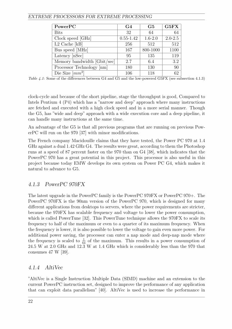
Table 4.1: Some of the differences between G4 and G5 and the low-powered G5FX (see subsection 4.1.3)
clock-cycle and because of the short pipeline, stage the throughput is good, Compared toIntels Pentium 4 (P4) which has a ”narrow and deep” approach where many instructionsare fetched and executed with a high clock speed and in a more serial manner. Thoughthe G5, has ”wide and deep” approach with a wide execution core and a deep pipeline, itcan handle many instructions at the same time.
An advantage of the G5 is that all previous programs that are running on previous Pow-erPC will run on the 970 [37] with minor modifications.
The French company Macidouille claims that they have tested, the Power PC 970 at 1.4GHz against a dual 1.42 GHz G4. The results were great, according to them the Photoshopruns at a speed of 87 percent faster on the 970 than on G4 [38], which indicates that thePowerPC 970 has a great potential in this project. This processor is also useful in thisproject because today EMW develops its own system on Power PC G4, which makes itnatural to advance to G5.
4.1.3 PowerPC 970FX
The latest upgrade in the PowerPC family is the PowerPC 970FX or PowerPC 970+. ThePowerPC 970FX is the 90nm version of the PowerPC 970, which is designed for manydifferent applications from desktops to servers, where the power requirements are stricter,because the 970FX has scalable frequency and voltage to lower the power consumption,which is called PowerTune [32]. This PowerTune technique allows the 970FX to scale itsfrequency to half of the maximum or even to a quarter of its maximum frequency. Whenthe frequency is lower, it is also possible to lower the voltage to gain even more power. Foradditional power saving, the processor can enter a nap mode and deep-nap mode wherethe frequency is scaled to 1
64of the maximum. This results in a power consumption of
24.5 W at 2.0 GHz and 12.3 W at 1.4 GHz which is considerably less than the 970 thatconsumes 47 W [39].
4.1.4 AltiVec
”AltiVec is a Single Instruction Multiple Data (SIMD) machine and an extension to thecurrent PowerPC instruction set, designed to improve the performance of any applicationthat can exploit data parallelism” [40]. AltiVec is used to increase the performance in
22
CHAPTER 4. PROCESSOR SURVEY
audio, video and communication applications. For using AltiVec, the developers do notneed to rewrite the entire application, but the application must be reprogrammed or atleast recompiled. Applications that use AltiVec do not require to be written in assembler.It is also possible to use C, C++ or Obj C for easier use.
Apple provides a number of highly tuned vector libraries such as a FFT suite of basicvector math routines, like sine, cosine and square root. Equation 4.1 shows calculatingthe theoretical peak performance of a 2.5 Ghz dual processor G5 machine:
(2.5x10⁹cycles/s) · (8FLOP/cycle) · (2processors) = 40GFLOPS (4.1)
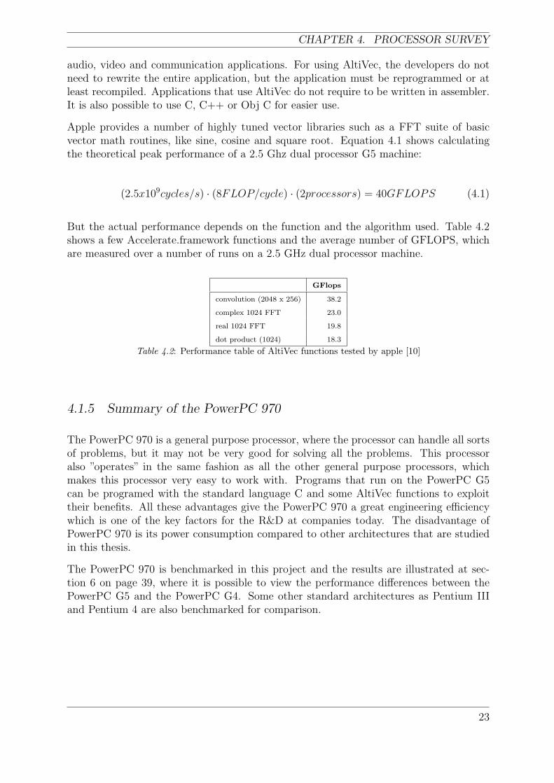
But the actual performance depends on the function and the algorithm used. Table 4.2shows a few Accelerate.framework functions and the average number of GFLOPS, whichare measured over a number of runs on a 2.5 GHz dual processor machine.
GFlops
convolution (2048 x 256) 38.2
complex 1024 FFT 23.0
real 1024 FFT 19.8
dot product (1024) 18.3
Table 4.2: Performance table of AltiVec functions tested by apple [10]
4.1.5 Summary of the PowerPC 970
The PowerPC 970 is a general purpose processor, where the processor can handle all sortsof problems, but it may not be very good for solving all the problems. This processoralso ”operates” in the same fashion as all the other general purpose processors, whichmakes this processor very easy to work with. Programs that run on the PowerPC G5can be programed with the standard language C and some AltiVec functions to exploittheir benefits. All these advantages give the PowerPC 970 a great engineering efficiencywhich is one of the key factors for the R&D at companies today. The disadvantage ofPowerPC 970 is its power consumption compared to other architectures that are studiedin this thesis.
The PowerPC 970 is benchmarked in this project and the results are illustrated at sec-tion 6 on page 39, where it is possible to view the performance differences between thePowerPC G5 and the PowerPC G4. Some other standard architectures as Pentium IIIand Pentium 4 are also benchmarked for comparison.
23
EXTREME PROCESSORS FOR EXTREME PROCESSING
4.1.6 Key features of PowerPC 970
Some interesting features of the PowerPC 970 are stated2 in this section.
Peak performance Power consumption7.2 GFLOPS 47 W at 1.8 GHzAltivec SIMD structure: 14.2 GFLOPS
On-chip memory Programming32 kB L1 Data cache Running on Power Mac G5512 kB L2 Cache
Application PerformanceThere are benchmarks at page 14 in section 3.3
4.2 ClearSpeed
Clearspeed is a company that manufactures extreme processors, which are high perfor-mance floating point co-processor based on a multi-threaded array of processors (MTAP).The architectural idea is to use many small processing elements which are set at low fre-quency to gain power. ClearSpeed has two processors called CS301 and CSX600 that areuseful for this project.
4.2.1 CS301
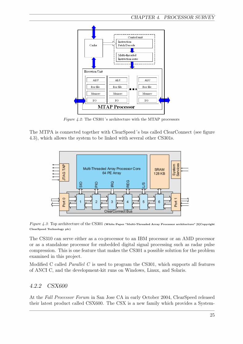
The architecture of the CS301 consists of an execution unit, a control unit, I/O and somecache. The control unit fetches, decodes and dispatches instructions to the executionunit (see figure 4.2). It also provides hardware support for the multi-threaded executionswhich allow fast exchanges between multiple threads; for example the parallel architectureresults in latencies when all PEs read/write to the same external memory at the sametime. The control unit solves this problem by giving the processor another code threadthat keeps the processor busy [5].
The execution unit on the CS301 is based on the 64 processing elements (PE). EachPE consists of a 32-bit ALU and two FPUs. It also includes an integer MAC, registers,memory and I/O. The PE´s processors are configurable which makes it possible to scalespecific applications. The execution unit can be divided into two parts. One part is themono execution unit, which is dedicated to do mono executions like scalar or non-paralleldata, and it handles the flow control of branching and thread switching. The remainderof the PEs are the poly execution unit which handles all parallel data. This unit, whichconsists of an array of PEs, operates comparable to an SIMD processor [5].
There are two different I/Os in the CS301 chip; one is Programmed I/O (PIO), which isused for accessing memory external to the core, and the other is Streaming I/O (SIO)which allows blocks of bordering to be streamed straight into the memory within PEs [5].
2The data in this section is taken from www-306.ibm.com [41]
24
CHAPTER 4. PROCESSOR SURVEY
Figure 4.2: The CS301´s architecture with the MTAP processors
The MTPA is connected together with ClearSpeed´s bus called ClearConnect (see figure4.3), which allows the system to be linked with several other CS301s.
Figure 4.3: Top architecture of the CS301 (White Paper ”Multi-Threaded Array Processor architecture” [5]Copyright
ClearSpeed Technology plc)
The CS310 can serve either as a co-processor to an IBM processor or an AMD processoror as a standalone processor for embedded digital signal processing such as radar pulsecompression. This is one feature that makes the CS301 a possible solution for the problemexamined in this project.
Modified C called Parallel C is used to program the CS301, which supports all featuresof ANCI C, and the development-kit runs on Windows, Linux, and Solaris.
4.2.2 CSX600
At the Fall Processor Forum in San Jose CA in early October 2004, ClearSpeed releasedtheir latest product called CSX600. The CSX is a new family which provides a System-
25
EXTREME PROCESSORS FOR EXTREME PROCESSING
on-a-Chip (SoC) solution with the MTAP processor core. The CSX600 also includes aDDR2-RAM interface and an on-chip SRAM.
The MTAP core consists of 96 VLIW PEs where each PE contains an integer ALU, 16-bitinteger MAC, 64-bit superscaler FPU as well as memory I/O and registers. This processoris ideally for applications with high processing and high bandwidth requirements. Theperformance data of the CSX600 is doubled up compared with the CS301.
4.2.3 Summary of ClearSpeeds processors
ClearSpeed´s processor which aims for low power consumption, remains a great floatingpoint calculating processor, because its PEs are entire processors with ALU, memoryand registers, which are the same as 64 resp 96 working processors. ClearSpeed saysthat ”ClearSpeed’s processors provide significant advances in performance and low powerconsumption while maintaining ease of programming”, which sums up the ClearSpeedtechnology well. The CS301 and the CSX600 have a very low power consumption whichenables the user to have several units to gain performance, but still does not have toworry about using too much power, which of course makes the system very complex. Toprogram ClearSpeed processors C is used which is good for the engineering efficiency, andClearspeed also offers a software development kit (SDK) with extensions to support theMTAP.
ClearSpeed also say that their processors are well suited for digital signal processing likeFFT, because there are complete libraries that support these functions. The results of abenchmark with FFT calculation made by Lockheed Martin are shown in table 7.1.
4.2.4 Key features of CS 301 and the CSX600
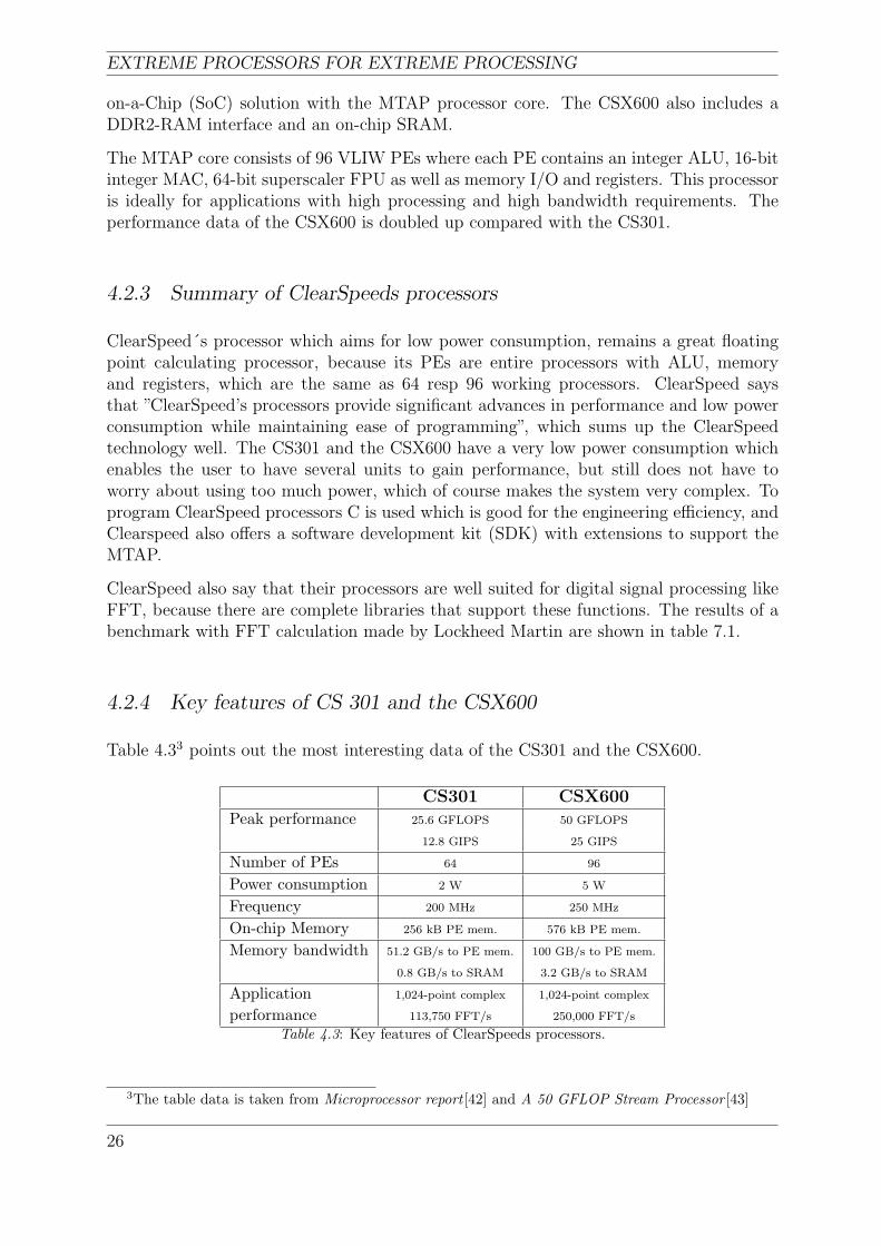
Table 4.33 points out the most interesting data of the CS301 and the CSX600.
CS301 CSX600Peak performance 25.6 GFLOPS 50 GFLOPS
12.8 GIPS 25 GIPS
Number of PEs 64 96
Power consumption 2 W 5 W
Frequency 200 MHz 250 MHz
On-chip Memory 256 kB PE mem. 576 kB PE mem.
Memory bandwidth 51.2 GB/s to PE mem. 100 GB/s to PE mem.
0.8 GB/s to SRAM 3.2 GB/s to SRAM
Application 1,024-point complex 1,024-point complex
performance 113,750 FFT/s 250,000 FFT/s
Table 4.3: Key features of ClearSpeeds processors.
3The table data is taken from Microprocessor report [42] and A 50 GFLOP Stream Processor [43]
26
CHAPTER 4. PROCESSOR SURVEY
4.3 PicoChip
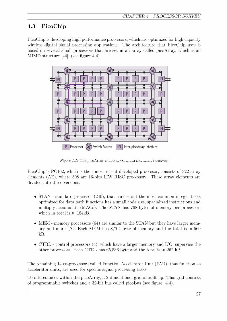
PicoChip is developing high performance processors, which are optimized for high capacitywireless digital signal processing applications. The architecture that PicoChip uses isbased on several small processors that are set in an array called picoArray, which is anMIMD structure [44], (see figure 4.4).
Figure 4.4: The picoArray (PicoChip ”Advanced information PC102”)[6]
PicoChip´s PC102, which is their most recent developed processor, consists of 322 arrayelements (AE), where 308 are 16-bits LIW RISC processors. These array elements aredivided into three versions.
• STAN - standard processor (240), that carries out the most common integer tasksoptimized for data path functions has a small code size, specialized instructions andmultiply-accumulate (MACs). The STAN has 768 bytes of memory per processor,which in total is ≈ 184kB.
• MEM - memory processors (64) are similar to the STAN but they have larger mem-ory and more I/O. Each MEM has 8,704 byte of memory and the total is ≈ 560kB.
• CTRL - control processors (4), which have a larger memory and I/O, supervise theother processors. Each CTRL has 65,536 byte and the total is ≈ 262 kB
The remaining 14 co-processors called Function Accelerator Unit (FAU), that function asaccelerator units, are used for specific signal processing tasks.
To interconnect within the picoArray, a 2-dimentionel grid is built up. This grid consistsof programmable switches and a 32-bit bus called picoBus (see figure 4.4).
27
EXTREME PROCESSORS FOR EXTREME PROCESSING
The AEs provide a theoretical peak performance of 197.1 Giga instructions per second(GIPS).Calculated as (Peak of 4 LIW instructions per operations)x(160 MHz clock)x(308 proces-sors per element)= 197.1 GIPS.But 2 LIW instructions per operations is more of an average assumption which resultsin a performance of 98.6 GIPS. Some interesting features on the PC 102 are shown intable 4.4.
Subject UnitFrequency 160 MHzOn-chip RAM 1003 kBExternal SRAM 8 (128) MBPeak processing capacity 197.1 GIPSPeak MAC 38,4 GMACLatency 55,6 us
Table 4.4: Key features PC102
As seen in figure 4.4, there is a specialized interface called Inter-picoArray Interface (IPI),which allows several PC102s to interconnect with each other to increase the processingcapability. There is also a second interface called Asynchronous Data Interface (ADI),that allows data to be switched between the picoBus and the external asynchronous datastream [6].
The software that picoChip developed is called picoTool, which contains compiler andsimulator that allow a design to be tested before it is downloaded to the PC102. PicoToolis also provided by libraries, like FFTs and FIR filters.
To program the PC102, most of the applications can be made in picoChip´s ANCI Ccompiler, and the time critical processes´s assembler is used. Then structural VHDL isused to get the logic synthesis [45].
4.3.1 Summary of PC 102
PicoCips PC 102 is a low power processor but it has no hardware support for floating-point calculations compared to ClearSpeeds. Anyway, this is a very powerful processor,because of its highly parallel architecture, and high-speed interconnection capabilities(Inter-picoArray Interface) which make it possible to connect it with several PC102s.However, the off-chip communication to RAMs is significantly less than the other proces-sors. The PC 102 is the best processor, performance wise, of all the analyzed processors.Because it has over 300 processing elements which is three times more than the Clear-Speeds CSX600 (see table 4.6 and 4.7). But the PC 102 does not handle floating-pointcalculations very efficiently. If floating-point calculations are needed, even PicoChip willrecommend ClearSpeeds processors[46]. A great benefit of the PC 102 processor is thatthey are easy to connect with several other PC 102s due to the IPI, and this gives the PC102 good connectivity.
According to picoChip, the PC 102 is ”surprisingly easy” to program. ”Each processoris orthogonal and only interacts through defined means; as such, there is no necessityfor the developer to explicitly ”manage” or coordinate them - that is all handled through
28
CHAPTER 4. PROCESSOR SURVEY
the toolflow.” [www.picochip.com]. Which is necessary, because it would not be easy tocontrol over 300 PEs.
4.3.2 Key features of PC 102
Some of the available data on PC 1024 is displayed in this section.
Peak performance Power consumption197.1 GIPS 6 W at 160 MHz
On-chip memory Memory bandwidth1003 kB SRAM 3.3 Tbit/s on-chip
20 Gbit/s I/O20MB/s to SRAM
Application Performance ProgrammingTable 4.4 Development kits are available
4.4 Intrinsity
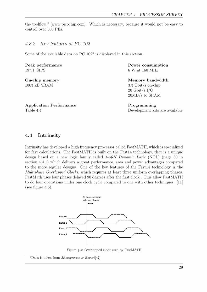
Intrinsity has developed a high frequency processor called FastMATH, which is specializedfor fast calculations. The FastMATH is built on the Fast14 technology, that is a uniquedesign based on a new logic family called 1-of-N Dynamic Logic (NDL) (page 30 insection 4.4.1) which delivers a great performance, area and power advantages comparedto the more regular designs. One of the key features of the Fast14 technology is theMultiphase Overlapped Clocks, which requires at least three uniform overlapping phases.FastMath uses four phases delayed 90 degrees after the first clock . This allow FastMATHto do four operations under one clock cycle compared to one with other techniques. [11](see figure 4.5).
Figure 4.5: Overlapped clock used by FastMATH
4Data is taken from Microprocessor Report [47]
29
EXTREME PROCESSORS FOR EXTREME PROCESSING
According to Intrinsity [48], a typical application for the FastMATH is cellular base sta-tions, radar, sonar and medical equipment such as ultrasound, x-ray and nuclear.
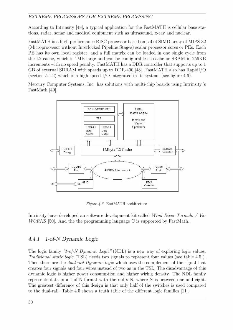
FastMATH is a high performance RISC processor based on a 4x4 SIMD array of MIPS-32(Microprocessor without Interlocked Pipeline Stages) scalar processor cores or PEs. EachPE has its own local register, and a full matrix can be loaded in one single cycle fromthe L2 cache, which is 1MB large and can be configurable as cache or SRAM in 256KBincrements with no speed penalty. FastMATH has a DDR controller that supports up to 1GB of external SDRAM with speeds up to DDR-400 [48]. FastMATH also has RapidI/O(section 5.1.2) which is a high-speed I/O integrated in its system, (see figure 4.6).
Mercury Computer Systems, Inc. has solutions with multi-chip boards using Intrinsity´sFastMath [49].
Figure 4.6: FastMATH architecture
Intrinsity have developed an software development kit called Wind River Tornado / Vx-WORKS [50]. And the the programming language C is supported by FastMath.
4.4.1 1-of-N Dynamic Logic
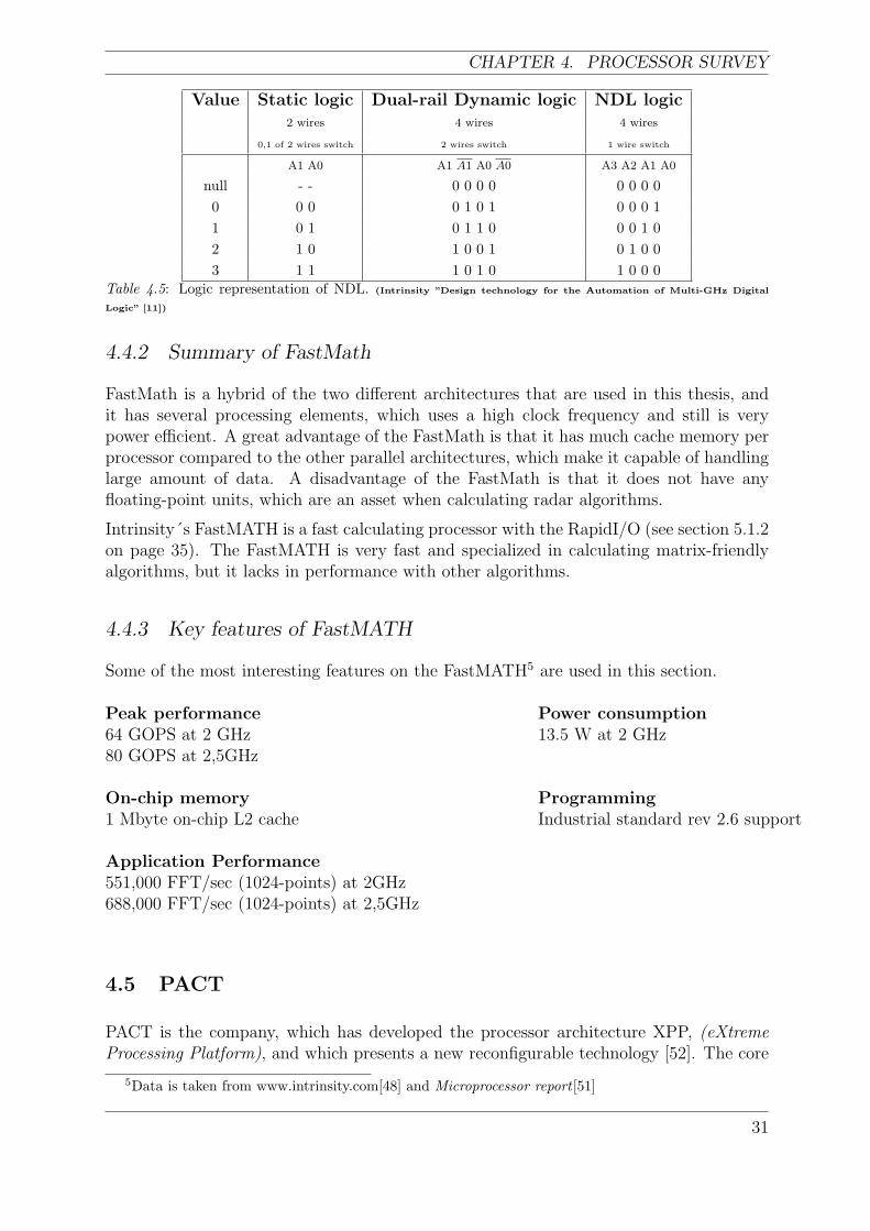
The logic family ”1-of-N Dynamic Logic” (NDL) is a new way of exploring logic values.Traditional static logic (TSL) needs two signals to represent four values (see table 4.5 ).Then there are the dual-rail Dynamic logic which uses the complement of the signal thatcreates four signals and four wires instead of two as in the TSL. The disadvantage of thisdynamic logic is higher power consumption and higher wiring density. The NDL familyrepresents data in a 1-of-N format with the radix N, where N is between one and eight.The greatest difference of this design is that only half of the switches is used comparedto the dual-rail. Table 4.5 shows a truth table of the different logic families [11].
30
CHAPTER 4. PROCESSOR SURVEY
Value Static logic Dual-rail Dynamic logic NDL logic2 wires 4 wires 4 wires
0,1 of 2 wires switch 2 wires switch 1 wire switch
A1 A0 A1 A1 A0 A0 A3 A2 A1 A0
null - - 0 0 0 0 0 0 0 00 0 0 0 1 0 1 0 0 0 11 0 1 0 1 1 0 0 0 1 02 1 0 1 0 0 1 0 1 0 03 1 1 1 0 1 0 1 0 0 0
Table 4.5: Logic representation of NDL. (Intrinsity ”Design technology for the Automation of Multi-GHz Digital
Logic” [11])
4.4.2 Summary of FastMath
FastMath is a hybrid of the two different architectures that are used in this thesis, andit has several processing elements, which uses a high clock frequency and still is verypower efficient. A great advantage of the FastMath is that it has much cache memory perprocessor compared to the other parallel architectures, which make it capable of handlinglarge amount of data. A disadvantage of the FastMath is that it does not have anyfloating-point units, which are an asset when calculating radar algorithms.
Intrinsity´s FastMATH is a fast calculating processor with the RapidI/O (see section 5.1.2on page 35). The FastMATH is very fast and specialized in calculating matrix-friendlyalgorithms, but it lacks in performance with other algorithms.
4.4.3 Key features of FastMATH
Some of the most interesting features on the FastMATH5 are used in this section.
Peak performance Power consumption64 GOPS at 2 GHz 13.5 W at 2 GHz80 GOPS at 2,5GHz
On-chip memory Programming1 Mbyte on-chip L2 cache Industrial standard rev 2.6 support
Application Performance551,000 FFT/sec (1024-points) at 2GHz688,000 FFT/sec (1024-points) at 2,5GHz
4.5 PACT
PACT is the company, which has developed the processor architecture XPP, (eXtremeProcessing Platform), and which presents a new reconfigurable technology [52]. The core
5Data is taken from www.intrinsity.com[48] and Microprocessor report [51]
31
EXTREME PROCESSORS FOR EXTREME PROCESSING
of the XPP is a high performance processor for streaming applications, which are able tocompute a lot of data at a low power consumption.
4.5.1 XPP architechture
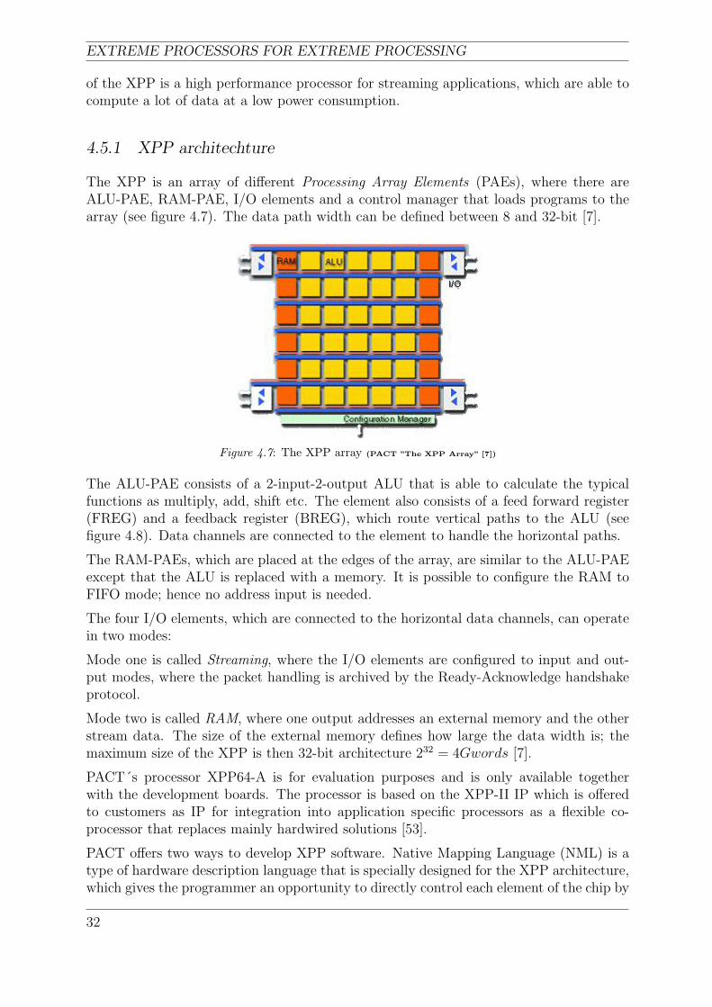
The XPP is an array of different Processing Array Elements (PAEs), where there areALU-PAE, RAM-PAE, I/O elements and a control manager that loads programs to thearray (see figure 4.7). The data path width can be defined between 8 and 32-bit [7].
Figure 4.7: The XPP array (PACT ”The XPP Array” [7])
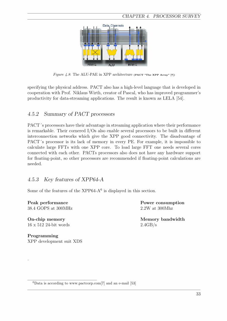
The ALU-PAE consists of a 2-input-2-output ALU that is able to calculate the typicalfunctions as multiply, add, shift etc. The element also consists of a feed forward register(FREG) and a feedback register (BREG), which route vertical paths to the ALU (seefigure 4.8). Data channels are connected to the element to handle the horizontal paths.
The RAM-PAEs, which are placed at the edges of the array, are similar to the ALU-PAEexcept that the ALU is replaced with a memory. It is possible to configure the RAM toFIFO mode; hence no address input is needed.
The four I/O elements, which are connected to the horizontal data channels, can operatein two modes:
Mode one is called Streaming, where the I/O elements are configured to input and out-put modes, where the packet handling is archived by the Ready-Acknowledge handshakeprotocol.
Mode two is called RAM, where one output addresses an external memory and the otherstream data. The size of the external memory defines how large the data width is; themaximum size of the XPP is then 32-bit architecture 232 = 4Gwords [7].
PACT´s processor XPP64-A is for evaluation purposes and is only available togetherwith the development boards. The processor is based on the XPP-II IP which is offeredto customers as IP for integration into application specific processors as a flexible co-processor that replaces mainly hardwired solutions [53].
PACT offers two ways to develop XPP software. Native Mapping Language (NML) is atype of hardware description language that is specially designed for the XPP architecture,which gives the programmer an opportunity to directly control each element of the chip by
32
CHAPTER 4. PROCESSOR SURVEY
Figure 4.8: The ALU-PAE in XPP architecture (PACT ”The XPP Array” [7])
specifying the physical address. PACT also has a high-level language that is developed incooperation with Prof. Niklaus Wirth, creator of Pascal, who has improved programmer’sproductivity for data-streaming applications. The result is known as LELA [54].
4.5.2 Summary of PACT processors
PACT´s processors have their advantage in streaming application where their performanceis remarkable. Their cornered I/Os also enable several processors to be built in differentinterconnection networks which give the XPP good connectivity. The disadvantage ofPACT´s processor is its lack of memory in every PE. For example, it is impossible tocalculate large FFTs with one XPP core. To load large FFT one needs several coresconnected with each other. PACTs processors also does not have any hardware supportfor floating-point, so other processors are recommended if floating-point calculations areneeded.
4.5.3 Key features of XPP64-A
Some of the features of the XPP64-A6 is displayed in this section.
Peak performance Power consumption38.4 GOPS at 300MHz 2.2W at 300Mhz
On-chip memory Memory bandwidth16 x 512 24-bit words 2.4GB/s
ProgrammingXPP development suit XDS
.
6Data is according to www.pactcorp.com[7] and an e-mail [53]
33
EXTREME PROCESSORS FOR EXTREME PROCESSING
4.6 Summary
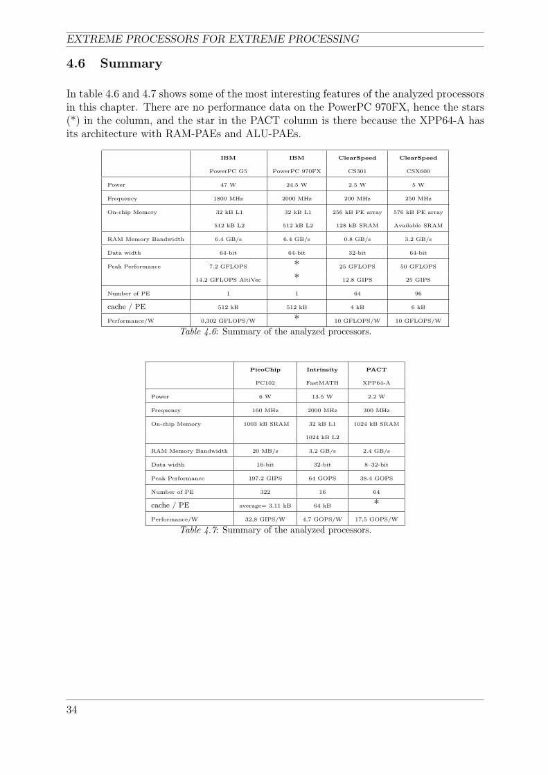
In table 4.6 and 4.7 shows some of the most interesting features of the analyzed processorsin this chapter. There are no performance data on the PowerPC 970FX, hence the stars(*) in the column, and the star in the PACT column is there because the XPP64-A hasits architecture with RAM-PAEs and ALU-PAEs.
IBM IBM ClearSpeed ClearSpeed
PowerPC G5 PowerPC 970FX CS301 CSX600
Power 47 W 24.5 W 2.5 W 5 W
Frequency 1800 MHz 2000 MHz 200 MHz 250 MHz
On-chip Memory 32 kB L1 32 kB L1 256 kB PE array 576 kB PE array
512 kB L2 512 kB L2 128 kB SRAM Available SRAM
RAM Memory Bandwidth 6.4 GB/s 6.4 GB/s 0.8 GB/s 3.2 GB/s
Data width 64-bit 64-bit 32-bit 64-bit
Peak Performance 7.2 GFLOPS * 25 GFLOPS 50 GFLOPS
14.2 GFLOPS AltiVec * 12.8 GIPS 25 GIPS
Number of PE 1 1 64 96
cache / PE 512 kB 512 kB 4 kB 6 kB
Performance/W 0,302 GFLOPS/W * 10 GFLOPS/W 10 GFLOPS/W
Table 4.6: Summary of the analyzed processors.
PicoChip Intrinsity PACT
PC102 FastMATH XPP64-A
Power 6 W 13.5 W 2.2 W
Frequensy 160 MHz 2000 MHz 300 MHz
On-chip Memory 1003 kB SRAM 32 kB L1 1024 kB SRAM
1024 kB L2
RAM Memory Bandwidth 20 MB/s 3.2 GB/s 2.4 GB/s
Data width 16-bit 32-bit 8–32-bit
Peak Performance 197.2 GIPS 64 GOPS 38.4 GOPS
Number of PE 322 16 64
cache / PE average= 3.11 kB 64 kB *Performance/W 32,8 GIPS/W 4,7 GOPS/W 17,5 GOPS/W
Table 4.7: Summary of the analyzed processors.
34
CHAPTER 5. INTERCONNECTION NETWORKS FOR MULTI-CHIP SYSTEMS
5 Interconnection networks for multi-chip systems
As discussed in the problem definition, it is clear that no commercial processor for thenear future is capable of handling a workload which demands TFLOPS in calculationspeed, or can handle the complexity in the future multipurpose AESA radar [13].
5.1 Interconnection networks
The classical solution for multiprocessing (MP) connections has been using parallel buseslike Peripheral Component Interconnect PCI, whose development are based on the abilityto increase the bus width and the frequency for gaining speedup. Unfortunately, thisdevelopment has reached fundamental limits, mainly due to clock skew, latency and pincount. When comparing the performance issue between the microprocessors that hasdoubled their performance every eighteen months (see section 2 on page 5) while the I/Obuses has doubled their performance approximately every three years. This has opened thedoor for new solutions. According to Carry D. Snyder [55], three promising solutions willbe presented and compared; two of which are 3rd Generation I/O (3GIO) and RapidIOwhich are based on a switching fabric, and the other one is the HyperTransport which isa PCI-type of architecture with a bus solution.
5.1.1 3GIO
The third generation I/O (3GIO) or PCI Express which was founded by Intel has focuson the PC market but it has also strong possibilities in embedded systems. The techniqueis developed by the PCI Special Interest Group (PCI SIG), which is based on key PCIattributes concerning usage model and software interfaces, but when as to the bandwidth-limiting the parallel bus is replaced by a fully serial interface to support multiple point-to-point connections[56]. This is done by replacing the multi-drop bus to a switch; whichcan either be a stand alone part of the system or integrated in the Host Bridge.
A basic connection built by different driven pairs of signals, can be scaled up to 32 lanewidth with an initial frequency of 2.5 Gbit/sec/direction, which could be increased in timeas the silicon technology advances [56]. The communication is a packet-based protocolwhich sends and receives packets through the I/O system.
5.1.2 RapidIO
The RapidIO which is developed by a trade association and controlled by its members,focuses on embedded systems which reflects the members, such as Mercury computersystems Inc. Motorola and IBM. The RapidIO concept that has a wide area of use asshown in figure 5.1, is mainly used in the embedded processor market.
35
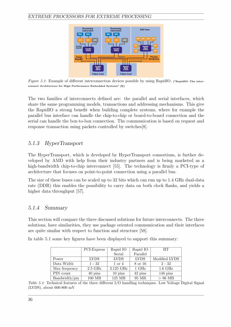
EXTREME PROCESSORS FOR EXTREME PROCESSING
Figure 5.1: Example of different interconnection devices possible by using RapidIO. (”RapidIO: The inter-
connect Architecture for High Performance Embedded Systems” [8])
The two families of interconnects defined are: the parallel and serial interfaces, whichshare the same programming models, transactions and addressing mechanisms. This givethe RapidIO a strong benefit when building complete systems, where for example theparallel bus interface can handle the chip-to-chip or board-to-board connection and theserial can handle the box-to-box connection. The communication is based on request andresponse transaction using packets controlled by switches[8].
5.1.3 HyperTransport
The HyperTransport, which is developed by HyperTransport consortium, is further de-veloped by AMD with help from their industry partners and is being marketed as ahigh-bandwidth chip-to-chip interconnect [55]. The technology is firmly a PCI-type ofarchitecture that focuses on point-to-point connection using a parallel bus.
The size of these buses can be scaled up to 32 bits which can run up to 1.4 GHz dual-datarate (DDR) this enables the possibility to carry data on both clock flanks, and yields ahigher data throughput [57].
5.1.4 Summary
This section will compare the three discussed solutions for future interconnects. The threesolutions, have similarities, they use package oriented communication and their interfacesare quite similar with respect to function and structure [58].
In table 5.1 some key figures have been displayed to support this summary:
PCI-Express Rapid IO Rapid IO HTSerial Parallel
Power LVDS LVDS LVDS Modified LVDSData Width 1 - 32 1 or 4 8 or 16 2 - 32Max frequency 2.5 GHz 3.125 GHz 1 GHz 1.6 GHzPIN count 40 pins 10 pins 42 pins 148 pinsBandwidth/pin 100 MB 125 MB 95 MB > 86 MB
Table 5.1: Technical features of the three different I/O handling techniques. Low Voltage Digital Signal(LVDS), about 600-800 mV
36
CHAPTER 5. INTERCONNECTION NETWORKS FOR MULTI-CHIP SYSTEMS
When comparing the three presented techniques, the focus has been on future possibilitiesand support instead of technical numbers where no solution is superior. The proposedsolution in this thesis will be RapidIO mainly due to its capabilities to support both”short” chip-to-chip communication using the parallel technique and ”longer” box-to-boxcommunication by serial technique through for example a backplane. The RapidIO, in thiscase, has also the best support from companies where among others one can find Motorola,IBM, Mercury computer systems Inc., Intrinsity and perhaps the most important Ericsson,which means that Ericsson can actively contribute to the development and get first handknowledge about the technology.
When drawing these conclusions one must keep in mind two things, first of all, no calcu-lations examples have been done in this project to investigate if the discussed techniquesare effective enough for future radar systems, but in the section 7.2 we have proposed afuture project that shall investigate it. The second thing one must keep in mind is that allthree techniques are in some what initial states of their development which means somemajor technical changes can appear in a near future.
37

EXTREME PROCESSORS FOR EXTREME PROCESSING
38
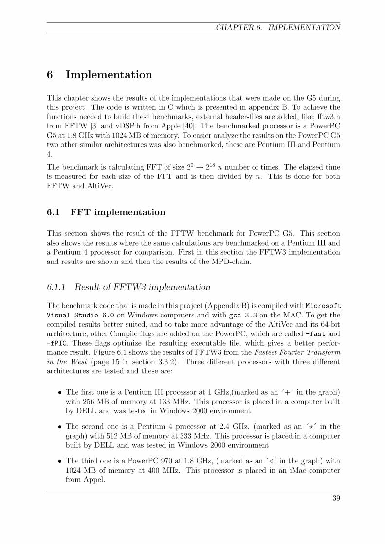
CHAPTER 6. IMPLEMENTATION
6 Implementation
This chapter shows the results of the implementations that were made on the G5 duringthis project. The code is written in C which is presented in appendix B. To achieve thefunctions needed to build these benchmarks, external header-files are added, like; fftw3.hfrom FFTW [3] and vDSP.h from Apple [40]. The benchmarked processor is a PowerPCG5 at 1.8 GHz with 1024 MB of memory. To easier analyze the results on the PowerPC G5two other similar architectures was also benchmarked, these are Pentium III and Pentium4.
The benchmark is calculating FFT of size 20 → 218 n number of times. The elapsed timeis measured for each size of the FFT and is then divided by n. This is done for bothFFTW and AltiVec.
6.1 FFT implementation
This section shows the result of the FFTW benchmark for PowerPC G5. This sectionalso shows the results where the same calculations are benchmarked on a Pentium III anda Pentium 4 processor for comparison. First in this section the FFTW3 implementationand results are shown and then the results of the MPD-chain.
6.1.1 Result of FFTW3 implementation
The benchmark code that is made in this project (Appendix B) is compiled with Microsoft
Visual Studio 6.0 on Windows computers and with gcc 3.3 on the MAC. To get thecompiled results better suited, and to take more advantage of the AltiVec and its 64-bitarchitecture, other Compile flags are added on the PowerPC, which are called -fast and-fPIC. These flags optimize the resulting executable file, which gives a better perfor-mance result. Figure 6.1 shows the results of FFTW3 from the Fastest Fourier Transformin the West (page 15 in section 3.3.2). Three different processors with three differentarchitectures are tested and these are:
• The first one is a Pentium III processor at 1 GHz,(marked as an ´+´ in the graph)with 256 MB of memory at 133 MHz. This processor is placed in a computer builtby DELL and was tested in Windows 2000 environment
• The second one is a Pentium 4 processor at 2.4 GHz, (marked as an ´?´ in thegraph) with 512 MB of memory at 333 MHz. This processor is placed in a computerbuilt by DELL and was tested in Windows 2000 environment
• The third one is a PowerPC 970 at 1.8 GHz, (marked as an ´/´ in the graph) with1024 MB of memory at 400 MHz. This processor is placed in an iMac computerfrom Appel.
39
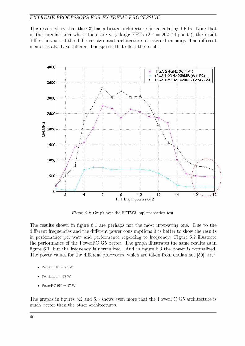
EXTREME PROCESSORS FOR EXTREME PROCESSING
The results show that the G5 has a better architecture for calculating FFTs. Note thatin the circular area where there are very large FFTs (218 = 262144-points), the resultdiffers because of the different sizes and architecture of external memory. The differentmemories also have different bus speeds that effect the result.
Figure 6.1: Graph over the FFTW3 implementation test.
The results shown in figure 6.1 are perhaps not the most interesting one. Due to thedifferent frequencies and the different power consumptions it is better to show the resultsin performance per watt and performance regarding to frequency. Figure 6.2 illustratethe performance of the PowerPC G5 better. The graph illustrates the same results as infigure 6.1, but the frequency is normalized. And in figure 6.3 the power is normalized.The power values for the different processors, which are taken from endian.net [59], are:
• Pentium III = 26 W
• Pentium 4 = 65 W
• PowerPC 970 = 47 W
The graphs in figures 6.2 and 6.3 shows even more that the PowerPC G5 architecture ismuch better than the other architectures.
40
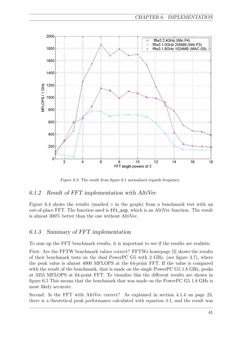
CHAPTER 6. IMPLEMENTATION
Figure 6.2: The result from figure 6.1 normalized regards frequency.
6.1.2 Result of FFT implementation with AltiVec
Figure 6.4 shows the results (marked ◦ in the graph) from a benchmark test with anout-of-place FFT. The function used is fft_zop, which is an AltiVec function. The resultis almost 300% better than the one without AltiVec.
6.1.3 Summary of FFT implementation
To sum up the FFT benchmark results, it is important to see if the results are realistic.
First: Are the FFTW benchmark values correct? FFTWs homepage [3] shows the resultsof their benchmark tests on the dual PowerPC G5 with 2 GHz, (see figure 3.7), wherethe peak value is almost 4000 MFLOPS at the 64-point FFT. If the value is comparedwith the result of the benchmark, that is made on the single PowerPC G5 1.8 GHz, peaksat 3355 MFLOPS at 64-point FFT. To visualize this the different results are shown infigure 6.5 This means that the benchmark that was made on the PowerPC G5 1.8 GHz ismost likely accurate.
Second: Is the FFT with AltiVec correct? As explained in section 4.1.4 on page 23,there is a theoretical peak performance calculated with equation 4.1, and the result was
41
EXTREME PROCESSORS FOR EXTREME PROCESSING
Figure 6.3: The result from figure 6.1 normalized regards to power.
40 GFLOPS with a dual G5 at 2.5 GHz. The real value was on the other hand 38.2GFLOPS. But the 1024-point complex FFT peaked at 23 GFLOPS according to table 4.2.According to equation 4.1, it is possible to divide the value with two, if only one processoris used, this will give an approximated value of 11.5 GFLOPS for the 1024-point complexFFT which is more comparable with results from the benchmark made in this project.As seen in figure 6.4, the benchmark peaked at 8.2 GFLOPS at 1024-points, which is arealistic value.
To prove that the resulting value of 8.2 GFLOPS is realistic, equation 4.1 is used again.The 2.5 GHz G5 theoretically peak at 40 GFLOPS, and the 1024-point complex FFTpeak really at 23 GFLOPS. The theoretical value divided by the 1024-point complex FFTresults in a factor for named σ for example, then:
σ = 4023
= 1.74
The theoretical peak value according to equation 4.1 for the 1.8 GHz single G5 is 14.4GFLOPS. Together with σ, a realistic value of how the 1.8 GHz G5 should perform canbe calculated as:
Realistic value for 1.8 GHz G5 = 14.4σ≈ 8.3
42
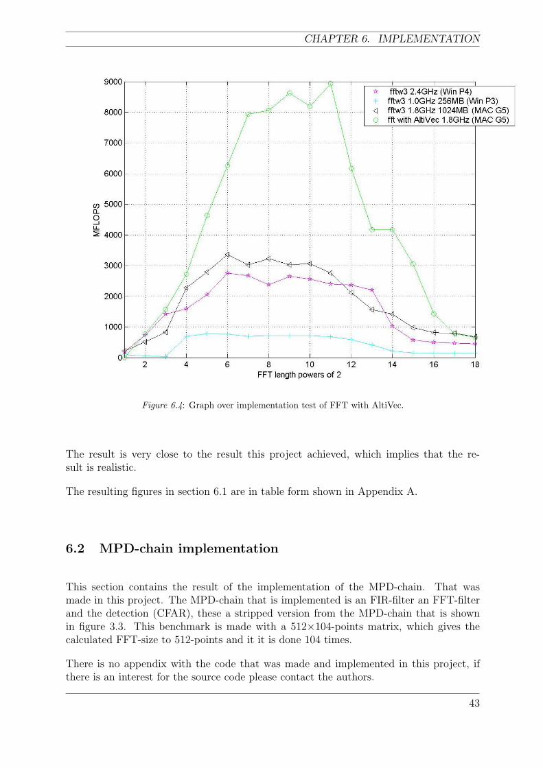
CHAPTER 6. IMPLEMENTATION
Figure 6.4: Graph over implementation test of FFT with AltiVec.
The result is very close to the result this project achieved, which implies that the re-sult is realistic.
The resulting figures in section 6.1 are in table form shown in Appendix A.
6.2 MPD-chain implementation
This section contains the result of the implementation of the MPD-chain. That wasmade in this project. The MPD-chain that is implemented is an FIR-filter an FFT-filterand the detection (CFAR), these a stripped version from the MPD-chain that is shownin figure 3.3. This benchmark is made with a 512×104-points matrix, which gives thecalculated FFT-size to 512-points and it it is done 104 times.
There is no appendix with the code that was made and implemented in this project, ifthere is an interest for the source code please contact the authors.
43
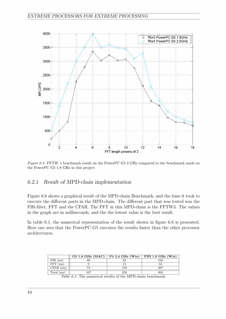
EXTREME PROCESSORS FOR EXTREME PROCESSING
Figure 6.5: FFTW´s benchmark result on the PowerPC G5 2 GHz compared to the benchmark made onthe PowerPC G5 1.8 GHz in this project
6.2.1 Result of MPD-chain implementation
Figure 6.6 shows a graphical result of the MPD-chain Benchmark, and the time it took toexecute the different parts in the MPD-chain. The different part that was tested was theFIR-filter, FFT and the CFAR. The FFT in this MPD-chain is the FFTW3. The valuesin the graph are in milliseconds, and the the lowest value is the best result.
In table 6.1, the numerical representation of the result shown in figure 6.6 is presented.Here one sees that the PowerPC G5 executes the results faster than the other processorarchitectures.
G5 1.8 GHz (MAC) P4 2.4 GHz (Win) PIII 1.0 GHz (Win)FIR (ms) 86 93 163FFT (ms) 9 15 54CFAR (ms) 72 150 387
Total (ms) 167 258 604
Table 6.1: The numerical results of the MPD-chain benchmark.
44
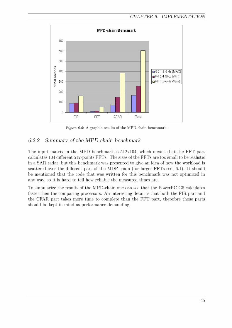
CHAPTER 6. IMPLEMENTATION
Figure 6.6: A graphic results of the MPD-chain benchmark.
6.2.2 Summary of the MPD-chain benchmark
The input matrix in the MPD benchmark is 512x104, which means that the FFT partcalculates 104 different 512-points FFTs. The sizes of the FFTs are too small to be realisticin a SAR radar, but this benchmark was presented to give an idea of how the workload isscattered over the different part of the MDP-chain (for larger FFTs see 6.1). It shouldbe mentioned that the code that was written for this benchmark was not optimized inany way, so it is hard to tell how reliable the measured times are.
To summarize the results of the MPD-chain one can see that the PowerPC G5 calculatesfaster then the comparing processors. An interesting detail is that both the FIR part andthe CFAR part takes more time to complete than the FFT part, therefore those partsshould be kept in mind as performance demanding.
45

EXTREME PROCESSORS FOR EXTREME PROCESSING
46
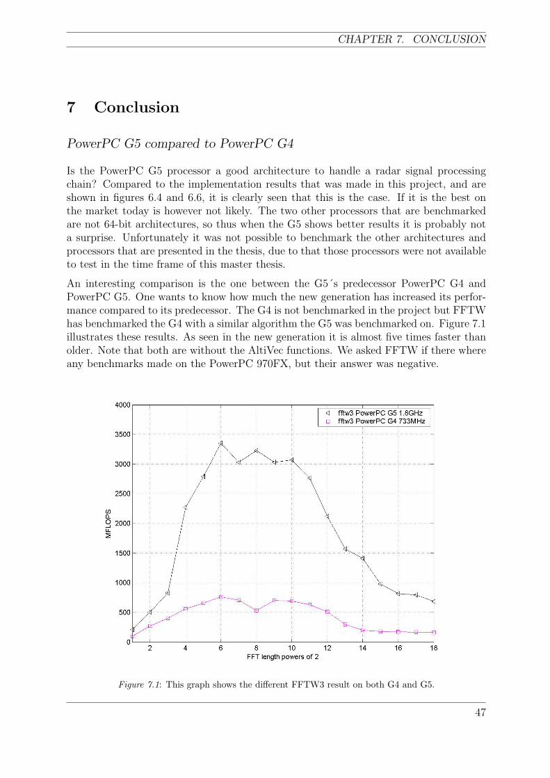
CHAPTER 7. CONCLUSION
7 Conclusion
PowerPC G5 compared to PowerPC G4
Is the PowerPC G5 processor a good architecture to handle a radar signal processingchain? Compared to the implementation results that was made in this project, and areshown in figures 6.4 and 6.6, it is clearly seen that this is the case. If it is the best onthe market today is however not likely. The two other processors that are benchmarkedare not 64-bit architectures, so thus when the G5 shows better results it is probably nota surprise. Unfortunately it was not possible to benchmark the other architectures andprocessors that are presented in the thesis, due to that those processors were not availableto test in the time frame of this master thesis.
An interesting comparison is the one between the G5´s predecessor PowerPC G4 andPowerPC G5. One wants to know how much the new generation has increased its perfor-mance compared to its predecessor. The G4 is not benchmarked in the project but FFTWhas benchmarked the G4 with a similar algorithm the G5 was benchmarked on. Figure 7.1illustrates these results. As seen in the new generation it is almost five times faster thanolder. Note that both are without the AltiVec functions. We asked FFTW if there whereany benchmarks made on the PowerPC 970FX, but their answer was negative.
Figure 7.1: This graph shows the different FFTW3 result on both G4 and G5.
47
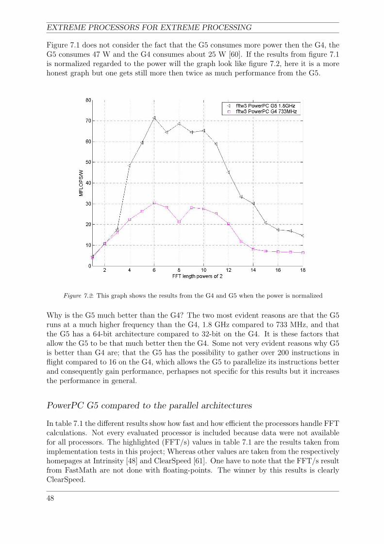
EXTREME PROCESSORS FOR EXTREME PROCESSING
Figure 7.1 does not consider the fact that the G5 consumes more power then the G4, theG5 consumes 47 W and the G4 consumes about 25 W [60]. If the results from figure 7.1is normalized regarded to the power will the graph look like figure 7.2, here it is a morehonest graph but one gets still more then twice as much performance from the G5.
Figure 7.2: This graph shows the results from the G4 and G5 when the power is normalized
Why is the G5 much better than the G4? The two most evident reasons are that the G5runs at a much higher frequency than the G4, 1.8 GHz compared to 733 MHz, and thatthe G5 has a 64-bit architecture compared to 32-bit on the G4. It is these factors thatallow the G5 to be that much better then the G4. Some not very evident reasons why G5is better than G4 are; that the G5 has the possibility to gather over 200 instructions inflight compared to 16 on the G4, which allows the G5 to parallelize its instructions betterand consequently gain performance, perhapses not specific for this results but it increasesthe performance in general.
PowerPC G5 compared to the parallel architectures
In table 7.1 the different results show how fast and how efficient the processors handle FFTcalculations. Not every evaluated processor is included because data were not availablefor all processors. The highlighted (FFT/s) values in table 7.1 are the results taken fromimplementation tests in this project; Whereas other values are taken from the respectivelyhomepages at Intrinsity [48] and ClearSpeed [61]. One have to note that the FFT/s resultfrom FastMath are not done with floating-points. The winner by this results is clearlyClearSpeed.
48
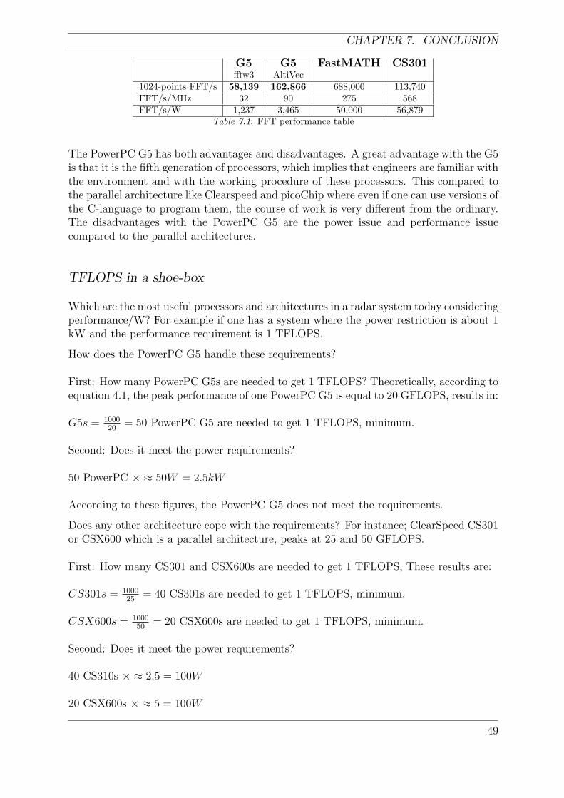
CHAPTER 7. CONCLUSION
G5 G5 FastMATH CS301fftw3 AltiVec
1024-points FFT/s 58,139 162,866 688,000 113,740FFT/s/MHz 32 90 275 568FFT/s/W 1,237 3,465 50,000 56,879
Table 7.1: FFT performance table
The PowerPC G5 has both advantages and disadvantages. A great advantage with the G5is that it is the fifth generation of processors, which implies that engineers are familiar withthe environment and with the working procedure of these processors. This compared tothe parallel architecture like Clearspeed and picoChip where even if one can use versions ofthe C-language to program them, the course of work is very different from the ordinary.The disadvantages with the PowerPC G5 are the power issue and performance issuecompared to the parallel architectures.
TFLOPS in a shoe-box
Which are the most useful processors and architectures in a radar system today consideringperformance/W? For example if one has a system where the power restriction is about 1kW and the performance requirement is 1 TFLOPS.
How does the PowerPC G5 handle these requirements?
First: How many PowerPC G5s are needed to get 1 TFLOPS? Theoretically, according toequation 4.1, the peak performance of one PowerPC G5 is equal to 20 GFLOPS, results in:
G5s = 100020
= 50 PowerPC G5 are needed to get 1 TFLOPS, minimum.
Second: Does it meet the power requirements?
50 PowerPC × ≈ 50W = 2.5kW
According to these figures, the PowerPC G5 does not meet the requirements.
Does any other architecture cope with the requirements? For instance; ClearSpeed CS301or CSX600 which is a parallel architecture, peaks at 25 and 50 GFLOPS.
First: How many CS301 and CSX600s are needed to get 1 TFLOPS, These results are:
CS301s = 100025
= 40 CS301s are needed to get 1 TFLOPS, minimum.
CSX600s = 100050
= 20 CSX600s are needed to get 1 TFLOPS, minimum.
Second: Does it meet the power requirements?
40 CS310s × ≈ 2.5 = 100W
20 CSX600s × ≈ 5 = 100W
49
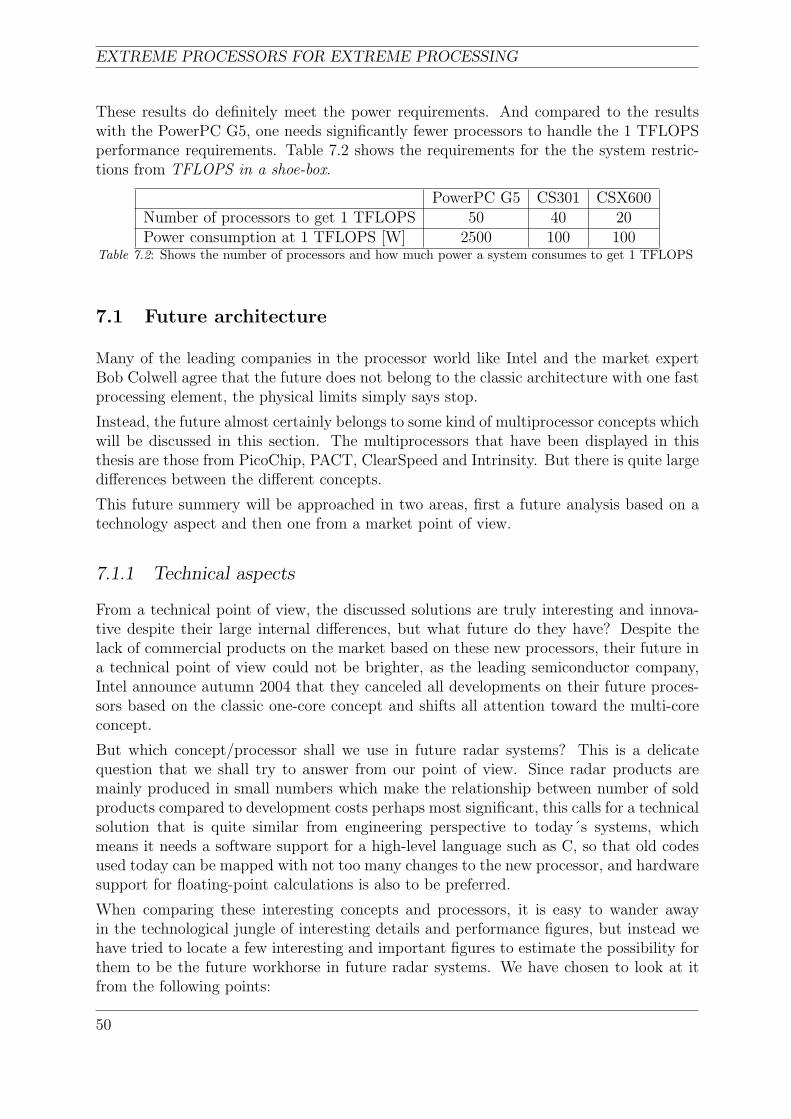
EXTREME PROCESSORS FOR EXTREME PROCESSING
These results do definitely meet the power requirements. And compared to the resultswith the PowerPC G5, one needs significantly fewer processors to handle the 1 TFLOPSperformance requirements. Table 7.2 shows the requirements for the the system restric-tions from TFLOPS in a shoe-box.
PowerPC G5 CS301 CSX600Number of processors to get 1 TFLOPS 50 40 20Power consumption at 1 TFLOPS [W] 2500 100 100
Table 7.2: Shows the number of processors and how much power a system consumes to get 1 TFLOPS
7.1 Future architecture
Many of the leading companies in the processor world like Intel and the market expertBob Colwell agree that the future does not belong to the classic architecture with one fastprocessing element, the physical limits simply says stop.
Instead, the future almost certainly belongs to some kind of multiprocessor concepts whichwill be discussed in this section. The multiprocessors that have been displayed in thisthesis are those from PicoChip, PACT, ClearSpeed and Intrinsity. But there is quite largedifferences between the different concepts.
This future summery will be approached in two areas, first a future analysis based on atechnology aspect and then one from a market point of view.
7.1.1 Technical aspects
From a technical point of view, the discussed solutions are truly interesting and innova-tive despite their large internal differences, but what future do they have? Despite thelack of commercial products on the market based on these new processors, their future ina technical point of view could not be brighter, as the leading semiconductor company,Intel announce autumn 2004 that they canceled all developments on their future proces-sors based on the classic one-core concept and shifts all attention toward the multi-coreconcept.
But which concept/processor shall we use in future radar systems? This is a delicatequestion that we shall try to answer from our point of view. Since radar products aremainly produced in small numbers which make the relationship between number of soldproducts compared to development costs perhaps most significant, this calls for a technicalsolution that is quite similar from engineering perspective to today´s systems, whichmeans it needs a software support for a high-level language such as C, so that old codesused today can be mapped with not too many changes to the new processor, and hardwaresupport for floating-point calculations is also to be preferred.
When comparing these interesting concepts and processors, it is easy to wander awayin the technological jungle of interesting details and performance figures, but instead wehave tried to locate a few interesting and important figures to estimate the possibility forthem to be the future workhorse in future radar systems. We have chosen to look at itfrom the following points:
50
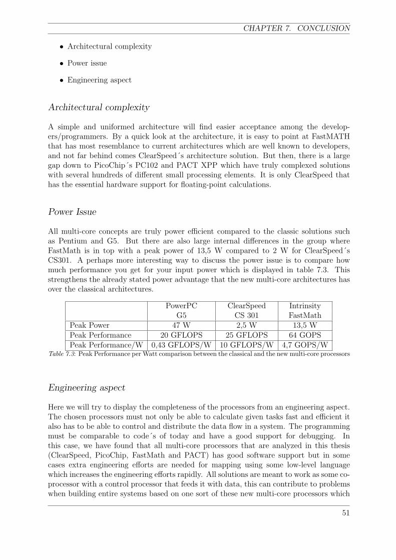
CHAPTER 7. CONCLUSION
• Architectural complexity
• Power issue
• Engineering aspect
Architectural complexity
A simple and uniformed architecture will find easier acceptance among the develop-ers/programmers. By a quick look at the architecture, it is easy to point at FastMATHthat has most resemblance to current architectures which are well known to developers,and not far behind comes ClearSpeed´s architecture solution. But then, there is a largegap down to PicoChip´s PC102 and PACT XPP which have truly complexed solutionswith several hundreds of different small processing elements. It is only ClearSpeed thathas the essential hardware support for floating-point calculations.
Power Issue
All multi-core concepts are truly power efficient compared to the classic solutions suchas Pentium and G5. But there are also large internal differences in the group whereFastMath is in top with a peak power of 13,5 W compared to 2 W for ClearSpeed´sCS301. A perhaps more interesting way to discuss the power issue is to compare howmuch performance you get for your input power which is displayed in table 7.3. Thisstrengthens the already stated power advantage that the new multi-core architectures hasover the classical architectures.
PowerPC ClearSpeed IntrinsityG5 CS 301 FastMath
Peak Power 47 W 2,5 W 13,5 WPeak Performance 20 GFLOPS 25 GFLOPS 64 GOPSPeak Performance/W 0,43 GFLOPS/W 10 GFLOPS/W 4,7 GOPS/W
Table 7.3: Peak Performance per Watt comparison between the classical and the new multi-core processors
Engineering aspect
Here we will try to display the completeness of the processors from an engineering aspect.The chosen processors must not only be able to calculate given tasks fast and efficient italso has to be able to control and distribute the data flow in a system. The programmingmust be comparable to code´s of today and have a good support for debugging. Inthis case, we have found that all multi-core processors that are analyzed in this thesis(ClearSpeed, PicoChip, FastMath and PACT) has good software support but in somecases extra engineering efforts are needed for mapping using some low-level languagewhich increases the engineering efforts rapidly. All solutions are meant to work as some co-processor with a control processor that feeds it with data, this can contribute to problemswhen building entire systems based on one sort of these new multi-core processors which
51
EXTREME PROCESSORS FOR EXTREME PROCESSING
is the best solution. Mixing different kinds of processors makes the developing complexityincrease rapidly but are perhaps necessary in future to reach the stated demands. In thiscase we have found Intrinsity´s and ClearSpeed´s solutions to have the biggest possibilitieswith an advantage for Intrinsty´s FastMATH that has clear hardware support for theseduties and has embedded support for the proposed I/O switching fabric RapidIO.
We feel that the solutions from Intrinsity and ClearSpeed current are to be prefered froma technical point of view with an overweight toward ClearSpeed´s solutions. We believethat the impressive solutions from PicoChip and PACT do not have their current futurein radar systems but one should not disregard them in future analysis. One must keep inmind that all the concepts are in some kind of initial work which makes it possible thatmuch can happen in a near future.
7.1.2 Market aspect
A major issue for the future is if these new companies and their impressive solutions willsurvive or if they will be out manoeuvred or bought by the market giants such as Intelor IBM. The key for success in our opinion is that the giants must change their researchdirection from their classical concepts toward these new concepts with a much brighterfuture. How can this be achieved?
The most effective way would be by starting some kind of joint project, such as thePowerPC cooperation between one or several larger market leading companies and smallercompanies that have their place, in the multiprocessor concept. The larger companies haveoften impressive strength when it comes to research budgets which no smaller companiescan get close to while the smaller can contribute with their perhaps more innovativethoughts and special knowledge in the multiprocessor concept. If the market finds fastacceptance to these new solutions, the giant companies risk to be outdistanced by thesmaller companies which aspired to become tomorrows giants.
7.2 Future Work
During this project we have identified two possible future projects which we will describein this section:
Implementation study of FastMATH and ClearSpeed
The first project would be an implementation study of the proposed future architecturesfrom Intrinsity and ClearSpeed. The optimal solution would be to implement the sameMPD-chain and FFTs as was done in this project to get as god comparison as possible.
The questions we would like to have answered in this project are what performance onecan get compared to the given optimal figures and how is the engineering efficiency forthese architectures.
52
CHAPTER 7. CONCLUSION
Implementation study of RapidIO
The second project that we suggest is a continuing on the work in chapter 5 where wepresented three possible candidates for future interconnection networks. We suggest aproject that has a similar disposition as this project, but instead of processors, the surveyshould handle future interconnection network techniques such as the three discussed inthis thesis. An implementation study should be conducted using RapidIO so that it canbe fully evaluated.
The question that this project should answer is if these new techniques can efficient coverthe needs in future extreme processing environments such as radar.
53

EXTREME PROCESSORS FOR EXTREME PROCESSING
54
BIBLIOGRAPHY
Bibliography
[1] Intel. (2004-11-09) Moore´s Law. [Online]. Available: http://www.intel.com/research/silicon/mooreslaw.htm
[2] T. Frisk, A. Ahlander, “Introduction to radar signal processing,” 1999, power Pointpresentation.
[3] Matteo Frigo and Steven G. Johnson. (2004-10-04) Fastest Fourier Transform in theWest. [Online]. Available: http://www.fftw.org/
[4] IBM. (2004-11-09) IBM PowerPC 970FX and networking applications. [Online].Available: http://www-306.ibm.com/g
[5] ClearSpeed, “Multi-Threaded Array Processor Architecture ,” White Paper 2004,2004-10-01.
[6] PicoChip, “Advanced Information PC102,” PC102-SFD v0.45, 2004-03-03.
[7] PACT. (2004-05-10) PACT Homepage. [Online]. Available: http://www.pactcorp.com/
[8] Dan Bouvier, “RapidIO: The interconnect Architecture for High Perfomance Embed-ded Systems.” White Paper, 2003.
[9] The Embedded Microprocessor Benchmark Consortium. (2004-10-01) About.[Online]. Available: http://www.eembc.hotdesk.com/
[10] Apple. (2004-12-01) Executive Summary. [Online]. Available: http://developer.apple.com/hardware/ve/summary.html
[11] Intrinsity, “Design Technology for the Automation of Multi-Gigahertz Digital Logic,” Fast14 Technology, 2004-10-05.
[12] G. Lindqvist, B. Widefeldt, JAS 39 GRIPEN. Nassjo: Air Historic Research AB,2003.
[13] P. Soderstam, A. Ahlander, “A future high-performance signal processing system,”1999, eMW Report.
[14] Wikipedia. (2004-05-10) Aperature radar. [Online]. Available: http://en.wikipedia.org/wiki/
[15] R. Karlsson B. Byline, “Extreme Processors for Extreme Processing study of highlyparallel architectures,” Master Thesis at Halmstad University 2005.
[16] Z. Ul-Abdin, O. Johnsson M. Stenemo,“Programming and implementation of stream-ing applications,” Master Thesis at Halmstad University 2005.
55
EXTREME PROCESSORS FOR EXTREME PROCESSING
[17] Lars Pettersson et.al, “An Experimental S-Band Digital Beamforming Antenna,”Conference paper, Oct 1996.
[18] U. Sjostrom et.al, “Design and Implementation of a Digital Down Converter Chip,”Conference paper, 1996.
[19] William S. Song et.al, “One trillion Operations per Second On-Board VLSI SIgnalProcessor for Discoverer II Space Based Radar,” Conference paper, March 2000.
[20] Military and Aerospace Electronics. (2004-05-3) Radar processing shifts to FPGAsand Altivec. [Online]. Available: http://mae.pennnet.com
[21] ——. (2004-05-3) Northrop Grumman wins 888 million dollar contract for advancedairborne radar. [Online]. Available: http://mae.pennnet.com
[22] F. Gunnarson and C. Hansson, “Embedded Supercomputers - A Study of ComputerArchitectures for Radar Signal Processing,” Master Thesis at Halmstad University2002.
[23] M.D. Godfrey and D.F. Hendry, “The Computer as von Neumann Planned It,” IEEEAnnals of the History of computing, 1993.
[24] Bob Colwell. (2004-11-10) Embedded Processors, No more hand-me-downs. [Online].Available: www.hh.se/ide/forskning/ceres
[25] E. Chu, A. George, Inside the FFT black box Serial and parallel fast fourier transforalgorithms. CRC Press, 2000.
[26] Steven W. Smith, Digital Signal Processing, Second Edition. Carlifonia TechnicalPublishing, 1999.
[27] Wikipedia. (2004-05-10) Fast Fourier transform. [Online]. Available: http://en.wikipedia.org/wiki/
[28] Relisoft. (2004-11-22) FFT. [Online]. Available: http://www.relisoft.com/Science/Physics/fft.html
[29] Skylondaworks. (2004-11-22) FFT butterfly Computation. [Online]. Available:http://www.skylondaworks.com/
[30] SPEC. (2004-10-21) SPECs homepage. [Online]. Available: http://www.spec.org
[31] ——. (2004-10-21) Q9: What source code is provided? [Online]. Available:http://www.spec.org/cpu2000/press/faq.html.dist
[32] Rohrer, N.J et al, “PowerPC 970 in 130 nm and 90 nm technologies,” 2004 IEEEInternational Solid-state Circuit conference, 2004-02-16.
[33] IBM. (2004-05-10) Power PC 970. [Online]. Available: http://www-306.ibm.com/
[34] apple. (2004-09-29) Technical Note TN2087. [Online]. Available: http://developer.apple.com/technotes/tn/tn2087.html
56
BIBLIOGRAPHY
[35] Wikipedia. (2004-05-10) IBM POWER. [Online]. Available: http://en.wikipedia.org/wiki/IBM POWER
[36] J. Stokes. (2004-09-29) Inside the IBM PowerPC 970. [Online]. Available:http://arstechnica.com/
[37] Momentum. (2004-05-10) 970 FAQ. [Online]. Available: http://www.970eval.com/
[38] J. Johansson. (2004-05-10) Forsta hastighetstestet av Power PC 970. [Online].Available: http://www.idg.se/
[39] IBM. (2004-11-22) Quick Reference Guide. [Online]. Available: http://www-306.ibm.com/
[40] Apple. (2004-09-27) Executive Summary. [Online]. Available: http://developer.apple.com/hardware/ve/summary.html
[41] P. Sandon. (2004-05-10) First in a new family of 64-bit high performance PowerPCprocessors. [Online]. Available: http://www-306.ibm.com/
[42] R.T. Halfhill, “Floating point buoys ClearSpeed,” Microprocessor Report 17 Nov,2003.
[43] S McIntosh Smith, “ClearSpeeds CSX600 ,” A 50 GFLOP Stream Processor, 2004-10-14.
[44] R.T. Halfhill, “PicoChip preaches Parallelism,” Microprocessor Report 28 July, 2003.
[45] PicoChip. (2004-05-10) PC102 Product Brief. [Online]. Available: http://www.picochip.com/technology/picoarray
[46] Rupert Baines at PicoChip. (2004-12-1) Personal e-mail conversation.
[47] R.T. Halfhill, “PicoChip makes a Big Mac,” Microprocessor Report 14 Oct, 2003.
[48] Intrinsity. (2004-05-10) Intrinsity Product Brief. [Online]. Available: http://www.intrinsity.com/
[49] Intrinsity, Mercury, “Multi-User Detection System Using the Intrinsity FastMATHProcessor,” White paper, www.intrinsity.com.
[50] Intrinsity. (2004-11-10) Intrinsity R© Evaluation Board Getting Started Guide.[Online]. Available: http://www.intrinsity.com/technology/documents.htm
[51] M. Baron, “Extremely High Performance,” Microprocessor Report 18 Feb, 2003.
[52] PACT corp. (2004-10-06) The XPP White paper release 2.1. [Online]. Available:http://www.pactcorp.com
[53] Eberhard Schueler at PACT. (2005-02-01) Personal e-mail conversation.
[54] P. N. Glaskowsky, “PACT debuts extreme processor,” Microprocessor Report 9 Sep,2000.
57
EXTREME PROCESSORS FOR EXTREME PROCESSING
[55] Carry D.Snyder, “Narrowed I/O Options Expand,” Microprocessor report 29 May,2001.
[56] Ajay V. Bhatt, “Creating a Third generation I/O interconnect.” White Paper, 2002.
[57] HyperTransport Consortium, “HyperTransport I/O Technology Comparison WithTraditional And Emerging I/O Technologies,” White Paper, June 2004.
[58] M.Gries et.al, “Developing a Flexible Interface for RapidIO, Hypertransport, andPCI-Express,” Conference paper, Sept 2004.
[59] endian.net. (2004-11-10) endian.net: Quick Specs Compared. [Online]. Available:http://endian.net
[60] Freescale semiconducter. (2004-11-10) MPC7455 : Host Processor. [Online].Available: http://www.freescale.com/webapp/sps/site/prod summary.jsp?code=MPC7455&nodeId=018rH3bTdG8653
[61] ClearSpeed. (2004-11-08) Digital Signal Processing . [Online]. Available: http://www.clearspeed.com
58
APPENDIX A. RESULT OF FFTW3 IMPLEMENTATION IN TABLE FORM
A Result of FFTW3 implementation in table form
Pentium IIIFFT length FLOPS FFT length FLOPS FFT length FLOPS
2 88 128 695 8,192 4164 54 256 715 16,384 2118 34 512 718 32,762 15016 699 1,024 714 65,536 14732 776 2,048 686 131,072 14164 773 4,096 585 262,144 137
Pentium 4FFT length FLOPS FFT length FLOPS FFT length FLOPS
2 179 128 2666 8,192 22074 725 256 2370 16,384 10258 1422 512 2644 32,762 57016 1584 1,024 2560 65,536 49932 2051 2,048 2406 131,072 47864 2757 4,096 2369 262,144 450
G5FFT length FLOPS FFT length FLOPS FFT length FLOPS
2 210 128 3030 8,192 15674 514 256 3225 16,384 14128 825 512 3030 32,762 97816 2272 1,024 3067 65,536 81632 2793 2,048 2762 131,072 79364 3355 4,096 2118 262,144 686
G5 with AltiVecFFT length FLOPS FFT length FLOPS FFT length FLOPS
2 * 128 7937 8,192 41674 771 256 8064 16,384 41678 1572 512 8620 32,762 304816 2717 1,024 8196 65,536 143132 4629 2,048 8929 131,072 77464 6250 4,096 6172 262,144 660
59

EXTREME PROCESSORS FOR EXTREME PROCESSING
60
APPENDIX B. BENCHMARK MAIN.C
B Benchmark main.c
#include <fftw3.h>#include <time.h>#include <sys/types.h>#include <stdio.h>#include <math.h>#include <stdlib.h>#include <string.h>#include <CoreServices/CoreServices.h>#include <vecLib/vDSP.h>#include <sys/types.h>#include "javamode.h"#include "main.h"#include <Carbon/Carbon.h>
#define START_POINTS 2#define STEP_NUM 18
double fftw3(int N, int numTries);void print_status(int numTries, double flops, double elapsedTime, double MFLOPS, int N,int tag);void matlab(double *MFLOPS,int F);double ComplexFFTUsageAndTimingOutOfPlace (int N, int numTries );//**********************************************************************************************main(void){int x, N, numTries, estMflops=500;double flops, MFLOPS_fftw, MFLOPS_fft_zop, elapsedTime_fftw, elapsedTime_fft_zop;double MFLOPS_FFTW3[STEP_NUM];double MFLOPS_FFT_ZOP[STEP_NUM];
printf("Benchmarking FFTW3...\n");
for(x=2;x<(STEP_NUM);x++){N=(int)(pow(2,(x+1)));
flops = 5*N*(log10(N) / log10(2));numTries = (int)(estMflops * 1e6 / flops * 10); //questimate 10 seconds
elapsedTime_fftw=fftw3(N, numTries);elapsedTime_fft_zop=ComplexFFTUsageAndTimingOutOfPlace (N, numTries );
MFLOPS_fftw = (double)(flops / ((elapsedTime_fftw/numTries) * 1e6));MFLOPS_fft_zop = (double)(flops / ((elapsedTime_fft_zop/numTries) * 1e6));
MFLOPS_FFTW3[x]=MFLOPS_fftw;MFLOPS_FFT_ZOP[x]=MFLOPS_fft_zop;
print_status(numTries, flops, elapsedTime_fftw, MFLOPS_fftw, N,1);print_status(numTries, flops, elapsedTime_fft_zop, MFLOPS_fft_zop, N,0);}
61
EXTREME PROCESSORS FOR EXTREME PROCESSING
matlab(MFLOPS_FFTW3,1);matlab(MFLOPS_FFT_ZOP,0);}//**********************************************************************************************double fftw3(int N, int numTries){int i=0;double elapsedTime;double startTime=0, endTime=0;
fftw_complex *in, *out;fftw_plan p;
// Allocate memory for the input & output operandsin = fftw_malloc(sizeof(fftw_complex) * N);out = fftw_malloc(sizeof(fftw_complex) * N);
// Creating Planp = fftw_plan_dft_1d(N, in, out, FFTW_FORWARD, FFTW_PATIENT);
// Timing section for the FFT.startTime = clock();for (i=0;i<numTries;i++){fftw_execute(p);}endTime = clock();
elapsedTime = (endTime-startTime) / CLOCKS_PER_SEC; // Tiden i Sec.
// Free allocated memory.fftw_destroy_plan(p);fftw_free(in); fftw_free(out);
return(elapsedTime);}//**********************************************************************************************double ComplexFFTUsageAndTimingOutOfPlace (int N, int numTries ){COMPLEX_SPLIT originalValue, A, result1;FFTSetup setup;UInt32 log2n;UInt32 n;SInt32 stride;SInt32 result1Stride;UInt32 i;float scale;double elapsedTime;double startTime=0, endTime=0;int N1=N;
n=N;log2n= log2(n);
stride = 1;result1Stride = 1;
62
APPENDIX B. BENCHMARK MAIN.C
printf ( "\n1D complex FFT out-of-place of length log2 ( %d ) = %d\n\n", (unsigned int)n,(unsigned int)log2n );
// Allocate memory for the input operands and check its availability.originalValue.realp = ( float* ) malloc ( n * sizeof ( float ) );originalValue.imagp = ( float* ) malloc ( n * sizeof ( float ) );A.realp = ( float* ) malloc ( n * sizeof ( float ) );A.imagp = ( float* ) malloc ( n * sizeof ( float ) );result1.realp = ( float* ) malloc ( n * sizeof ( float ) );result1.imagp = ( float* ) malloc ( n * sizeof ( float ) );
if( originalValue.realp == NULL || originalValue.imagp == NULL || A.realp == NULL|| A.imagp == NULL || result1.realp == NULL || result1.imagp == NULL )
{printf( "\nmalloc failed to allocate memory for the FFT section of the test.\n");exit(0);}
// Set the input vector of length n: [(1+j1),...,(1+j1)], where j^2 = -1.for ( i = 0; i < n; i++ ){originalValue.realp[i] = ( float ) ( i + 1 );originalValue.imagp[i] = 0.0;}
memcpy ( A.realp, originalValue.realp, ( n * sizeof ( float ) ) );memcpy ( A.imagp, originalValue.imagp, ( n * sizeof ( float ) ) );
// Set up the required memory for the FFT routines and check its availability.setup = create_fftsetup ( log2n, FFT_RADIX2 );if( setup == NULL ){printf ( "\nFFT_Setup failed to allocate enough memory.\n" );exit ( 0 );}
// Carry out a Forward and Inverse FFT transform, check for errors.fft_zop ( setup, &A, stride, &result1, result1Stride, log2n, FFT_FORWARD );fft_zop ( setup, &result1, result1Stride, &result1, result1Stride, log2n, FFT_INVERSE );
// Verify correctness of the results.scale = ( float ) 1.0 / n;
vsmul( result1.realp, 1, &scale, result1.realp, 1, n );vsmul( result1.imagp, 1, &scale, result1.imagp, 1, n );
// Timing section for the FFT.{
startTime = clock();for ( i = 0; i < numTries; i++ ){fft_zop ( setup, &A, stride, &result1, result1Stride, log2n, FFT_FORWARD );}endTime = clock();
63
EXTREME PROCESSORS FOR EXTREME PROCESSING
}
// Free allocated memory.destroy_fftsetup ( setup );free ( originalValue.realp );free ( originalValue.imagp );free ( A.realp );free ( A.imagp );free ( result1.realp );free ( result1.imagp );return(elapsedTime);}//**********************************************************************************************void print_status(int numTries, double flops, double elapsedTime, double MFLOPS, int N, int tag){if(tag==1){printf("\n");printf("*********************************************\n");printf("Result of FFTW3 %d-points FFT\n", N);printf("*********************************************\n");}else if(tag==0){printf("\n");printf("*********************************************\n");printf("Result of FFT ZIP %d-points FFT\n", N);printf("*********************************************\n");}printf ("Number of Tries:\t\t%d\n", numTries);printf ("FLOPS:\t\t\t\t%.f\n", flops);printf ("CPU Time (Seconds):\t\t%.3f\n", elapsedTime);printf ("Time for one FFT (uSeconds):\t%f\n", (elapsedTime/numTries) * 1e6);printf ("MFLOPS:\t\t\t\t%.2f\n", MFLOPS);}//**********************************************************************************************void matlab(double *MFLOPS, int F){int x;FILE *out;
// Creating MATLAB script(.m) over dataif(F==1){out = fopen("Benchmark_G5_fftw.m", "w");}else if(F==0){out = fopen("Benchmark_G5_fftzop.m", "w");}
fprintf(out, "powers = 1:%i;\n", STEP_NUM);fputs("points = 2.^powers;\n", out);fputs("fftw3 = [ ", out);
for(x=0;x!=STEP_NUM;x++){
64
APPENDIX B. BENCHMARK MAIN.C
fprintf(out, "%.2f", MFLOPS[x]);fputs(" ", out);}
fputs("];\n", out);fputs("figure(1)\n", out);fputs("plot(powers,fftw3,’*b’);\n", out);fputs("hold on\n", out);fputs("plot(powers,fftw3,’b’);\n", out);fputs("xlabel(’FFT length’);\n", out);fputs("ylabel(’MFLOPS’);\n", out);fprintf(out, "AXIS([1 %i 0 4000]);\n", STEP_NUM);fputs("legend(’fftw3 (MAC)’);\n", out);fputs("grid on;\n", out);}//**********************************************************************************************
65