Embed Size (px)
Citation preview

Technical Document
Model: F120
Name: F120 PCBA Service Manual
No.:
Version: V1.0
Drawn wanglinwen
Check
Sign
Standard
Approved
Page 2 of 26
Amendment Records
No. Version Drawn/
Amender Date Reason
Brief Introduction
1.0 2013-4-17
Note1: Fill in this table when you amend it every time. Note2: When you file it for the first time, write “None” in the “Reason” and “Brief Introduction”.
Page 3 of 26
Contents 1 Brief Introduction ................................................................................................................... 5 2 Security Items ........................................................................................................................ 5
2.1 Brief Notices ............................................................................................................... 5 2.2 Equipments Notices ................................................................................................. 5
3 Test Tools & Setup ................................................................................................................ 5 3.1 Test Tools .................................................................................................................... 5 3.2 Tool Settings............................................................................................................... 5
4 PCBA ....................................................................................................................................... 6 4.1 Top Side ...................................................................................................................... 6 4.2 Bottom Side ................................................................................................................ 7
5 Base Band Elements & Circuit Analysis .......................................................................... 7 5.1 SC6531 Typical Application .................................................................................... 8 5.2 System Clock ............................................................................................................. 8 5.3 Power Management ................................................................................................. 9 5.4 Storage Interface ....................................................................................................... 9 5.5 Audio Interface .......................................................................................................... 9 5.6 SIM Interface.............................................................................................................. 9 5.7 Keypad Interface ..................................................................................................... 10 5.8 Charging Circuit ...................................................................................................... 11 5.9 LCD Interface ........................................................................................................... 12
6 Power-on Procedure .......................................................................................................... 13 7 RF Elements ........................................................................................................................ 13
7.1 RF Structure ............................................................................................................. 13 7.2 SC2661 Introduction ........................................................................................... 13 7.3 RX Loop .................................................................................................................... 13 7.4 TX Loop ..................................................................................................................... 14 7.5 RF FAQ ..................................................................................................................... 14 7.6 BUG Analysis ........................................................................................................... 14
8 Trouble & Service ............................................................................................................... 15 8.1 Cannot Download ................................................................................................... 15 8.2 Cannot Power on .................................................................................................... 17 8.3 LCD Problem ........................................................................................................... 17
8.3.1 Black Screen ................................................................................................ 17 8.3.2 White, Mess, Blue Screen......................................................................... 17
8.4 Keypad Invalid ......................................................................................................... 18 8.5 Motor Problem ......................................................................................................... 18
8.5.1 Cannot Vibrate ............................................................................................. 18 8.5.2 Vibrate with Power-on ................................................................................ 18
8.6 Earphone Circuit Problem ..................................................................................... 19 8.6.1 Cannot Check Earphone ........................................................................... 19 8.6.2 Cannot Answer Calls .................................................................................. 19
Page 4 of 26
8.6.3 None in-out ................................................................................................... 19 8.7 Audio Circuit Problem ............................................................................................ 20
8.7.1 RECIEVER Silence .................................................................................... 21 8.7.2 MIC Silence .................................................................................................. 21
8.8 Camera Problem ..................................................................................................... 21 8.8.1 Not Ready ..................................................................................................... 22 8.8.2 Mess Screen ................................................................................................ 22
8.9 T-Flash Problem ...................................................................................................... 22 8.9.1 Cannot Identify Card .................................................................................. 22 8.9.2 Cannot Read Data ...................................................................................... 22
8.10 SIM Problem ............................................................................................................ 22 8.11 MP3 Problem ........................................................................................................... 23 8.12 Cannot Charged ...................................................................................................... 23 8.13 Cannot Write S/N .................................................................................................... 24 8.14 BT Station ................................................................................................................. 25
Page 5 of 26
1 Brief Introduction F120 is the phone of GSM&GSM dual standby but single using: SC6531 GSM base band chip, integrated with MCU and DSP part such as CPU in PC; SC2661 is the RF PA chip which deals with the power control of RF; Flash makes up of flash ROM and UtRAM. Please read this document to be familiar with the phone, refer it to maintain the PCBA.
2 Security Items Before maintain, please remember the items as follows:
2.1 Brief Notices
The phone makes up of many integrate circuit and electric components; do not use them in dusty, humidity and dirty area. The some components has polarity, static sensitivity, please do not touch it by hand at the best, and the iron and instrument must be grounded. Please refer to the notice on every instrument.
2.2 Equipments Notices
Please refer to the user guides of the equipments.
3 Test Tools & Setup
3.1 Test Tools
Wireless general-purpose tester, such as CMD55, Agilent8960, CMU200 Signal source Stroboscope HP high frequency test probe Oscillograph Digital Power Multimeter Clamping Level translation board or USB translation cable
3.2 Tool Settings
Supply an external power connect VBAT (3.8V DC, 1.0A), use the digital power best to view the changes. Please refer to the user guides of the equipments.

Page 6 of 26
4 PCBA
4.1 Top Side
Page 7 of 26
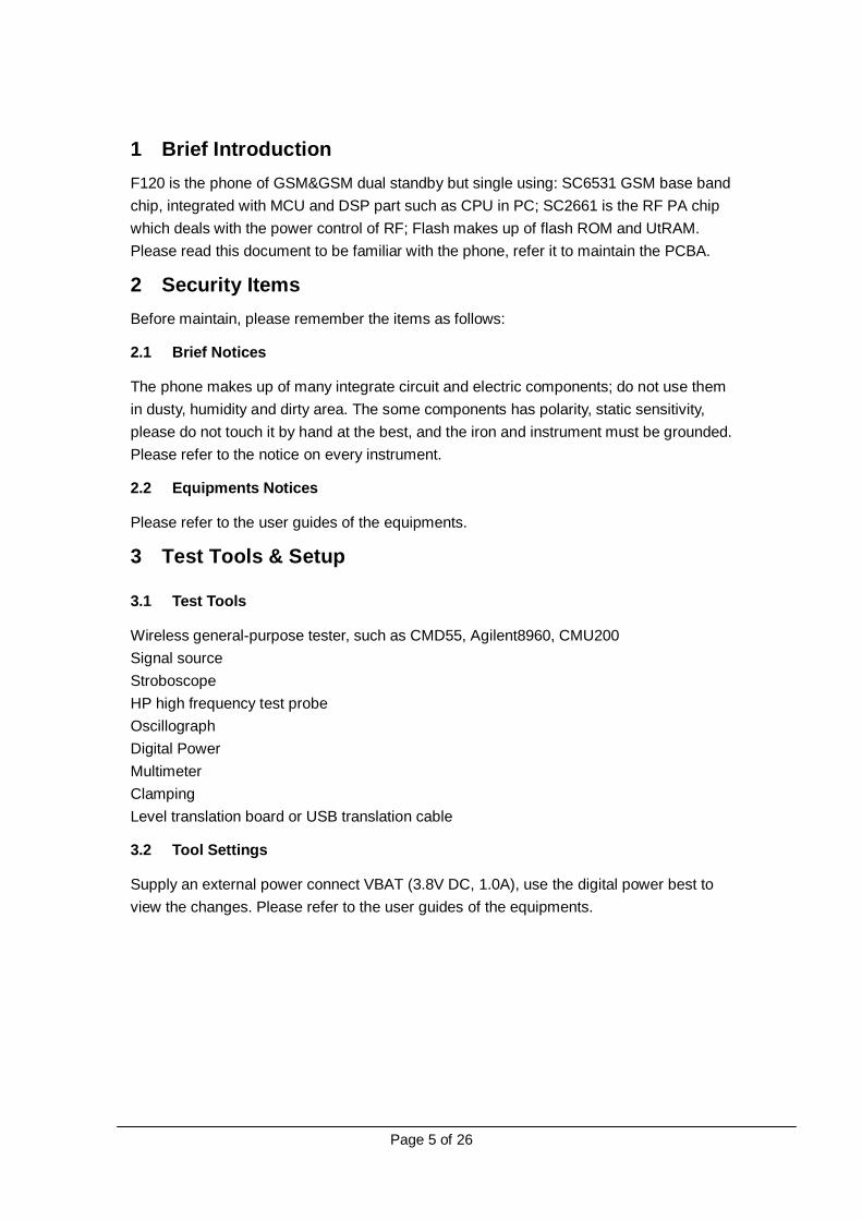
4.2 Bottom Side
5 Base Band Elements & Circuit Analysis The main module includes all the functions: LCD display, Speaker, Keypad, T-flash card, Camera, charging, etc.
Page 8 of 26
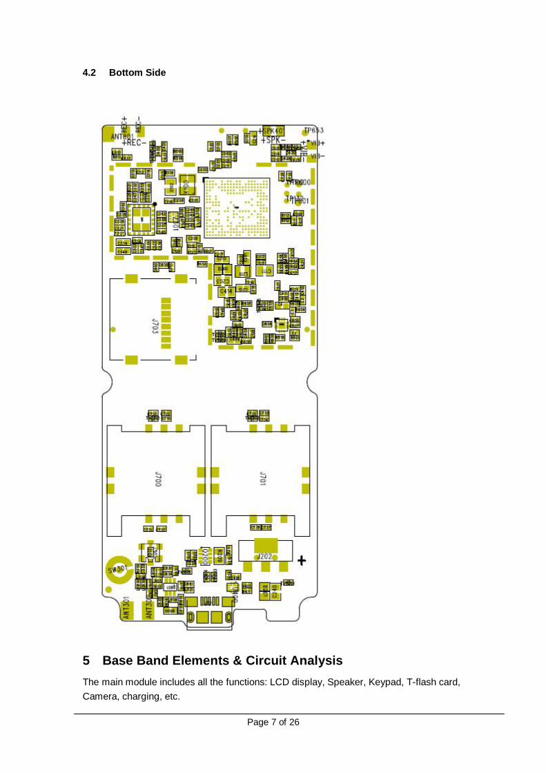
5.1 SC6531 Typical Application
SC6531 is a highly integrated single chip with embedded baseband, PSRAM and RF transceiver for GSM/GPRS applications, which is designed to provide a cost-effective, low-power and high-performance solution for mobile phones.SC6531 consists of an embedded 32-bit microcontroller and an embedded 16-bit DSP core with the specially optimized architecture and dedicated accelerators.The integrated RF transceiver provides the function of radio frequency signal transmition and receiving from or to baseband signal.
5.2 System Clock Clock is the base of control in every system. It has two types of clock in system: 32.768KHZ clock to display the time by system ; the other one is working clock, supplied by X100 (26MHZ crystal). 1)RTC——Real Time Clock: Generally, the RTC circuit is supplied by VBAT of the main battery. 2)System Clock Circuit: The clock of module is supplied by X100 (26MHZ crystal), and supply the consult clock to

Page 9 of 26
base band circuit and RF circuit.
5.3 Power Management SC6531 supplies power to the main module, and the voltage of all ports, LED driver, alerter driver, Charging Management, SIM card port, etc. One base band voltage abnormality would cause the phone cannot power on or cannot download software. And the 26MHz and 32.768 KHz would affect the power-on or download. Because the digit circuit needs the clock signal to work. The power management IC supplies the voltages as follows:
LDO Output
Voltage(V) Description
VDDSD 3.0 SD
VDD18 1.8 IO/Nand/LCM
VDD28 2.8 IO/Nand/LCM
VDDCAMD0 1.8 Sensor core
VDDCAMA 2.8 Sensor analog,Sensor IO,FM
VDDRF 2.85 GSM/GPRS RF
VDDSIM0 3.0/1.8 SIM card 1
VDDSIM1 3.0/1.8 SIM card 2
VDDCORE 1.1 CORE
5.4 Storage Interface SPI-compatible serial bus interface 1, SC6531D is a integrated 32Mbits ROM and 32Mbits RAM;
5.5 Audio Interface The audio interface includes MIC bias circuit, Earphone bias circuit, Earphone circuit, Receiver circuit, Speaker circuit. The MIC need bias circuit, and the bias circuit is supplied by CPU, and the driver of the receiver also supplied by CPU directly. So the exterior equipment is simple, only physics connected. The speaker shared with ring tone, MP3 and hand free, so use the audio amplifier to output big power. But the speaker now is used the internal audio PA, the exterior equipment is also simple, only physics connected.
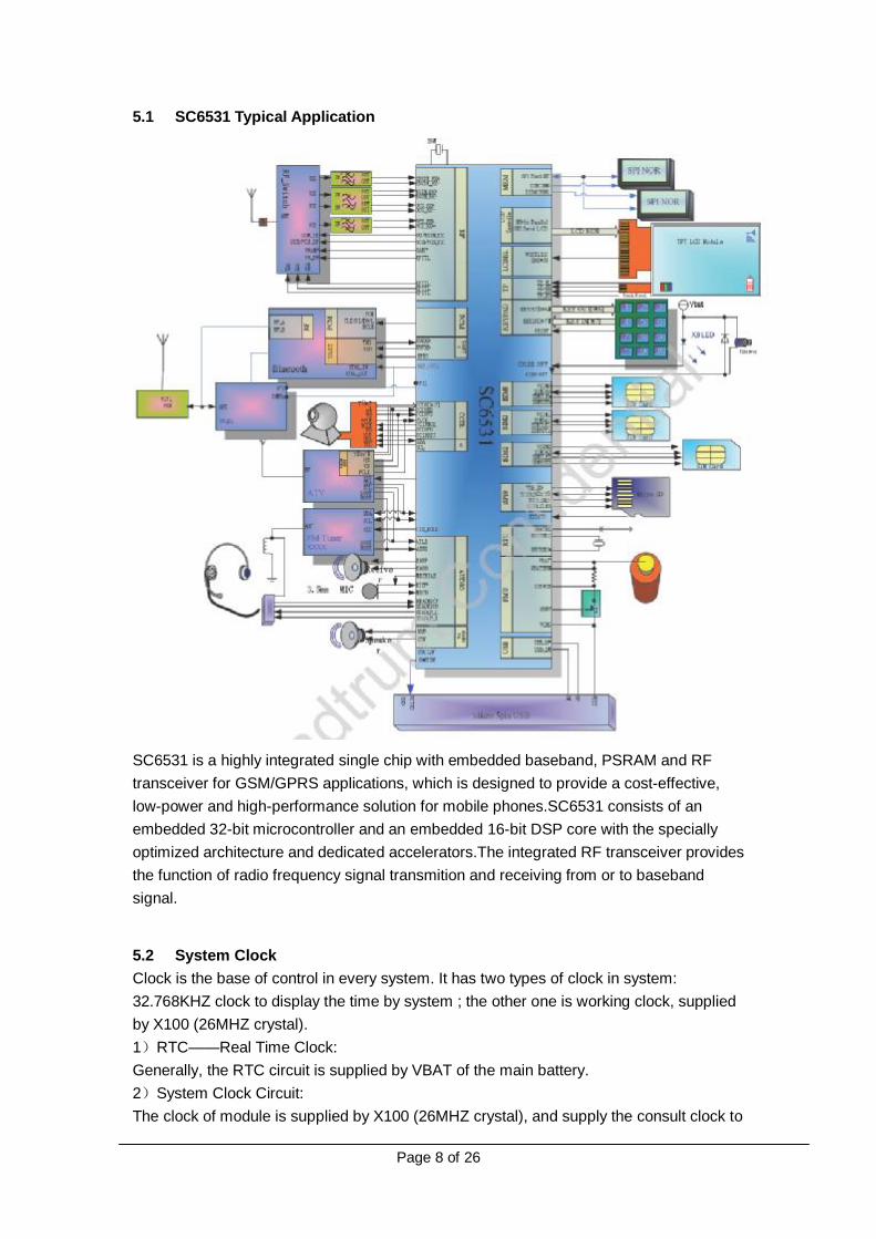
5.6 SIM Interface The phone compatibles with 1.8V, 3V SIM card and the MCU read-write it through dual serial bus.
Page 10 of 26
Fig. Dual-SIM cards Interface
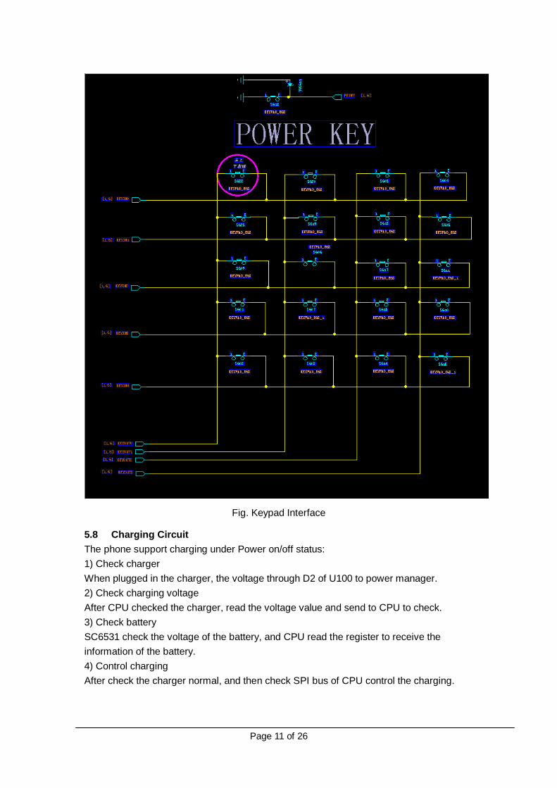
5.7 Keypad Interface The key part is made on the PCBA
Page 11 of 26
Fig. Keypad Interface
5.8 Charging Circuit The phone support charging under Power on/off status: 1) Check charger When plugged in the charger, the voltage through D2 of U100 to power manager. 2) Check charging voltage After CPU checked the charger, read the voltage value and send to CPU to check. 3) Check battery SC6531 check the voltage of the battery, and CPU read the register to receive the information of the battery. 4) Control charging After check the charger normal, and then check SPI bus of CPU control the charging.
Page 12 of 26
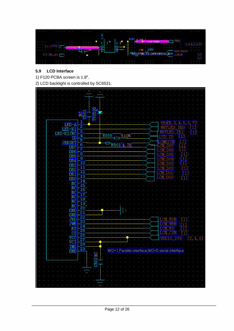
5.9 LCD Interface 1) F120 PCBA screen is 1.8″. 2) LCD backlight is controlled by SC6531.
Page 13 of 26
6 Power-on Procedure 1.Supply Power firstly, after PMU of SC6531 has V-BAT, it supplies 1.1V voltage to LDO interior of PMU and supplies VRTC (1.8V) to RTC of CPU. When CPU received the VRTC, 32.768K clock crystal and RTC begin to work; PMU and CPU will be idle status. 2. After press POWERON-KEY, PMU and CPU receive the power-on signal and PMU supplies VCORE (CPU supply power 1.1V), VDD18 (IO/NAND/LCM power 1.8V), VDD28 (IO/NAND/LCM power 2.8V),, VSIM (3V flash supply power).Meanwhile, VCORE, VDD and VMEM supply power to CPU , VSIM supply power to SIM card. 3. After CPU receive the signal and power supply, it output a control signal VCXO-EN to PMU and IC. When PMU receive VCXO-EN, it send signal to PMIC and then PMIC control 26M crystal and supply benchmark clock to base band circuit through IC. 4. After 26M crystal work steadily, CPU and PMU begin to reset. 5. After CPU reset, read the basic information of power-on from ROM and check the connection through the special key-press (KEYIN0\KEYOUT0 ). If this key is pressed, it would begin to download, otherwise, CPU execute the ROM program, open the bus to send the signal and then execute the file in flash, open the backlight and screen to enter the power-on mode.
7 RF Elements
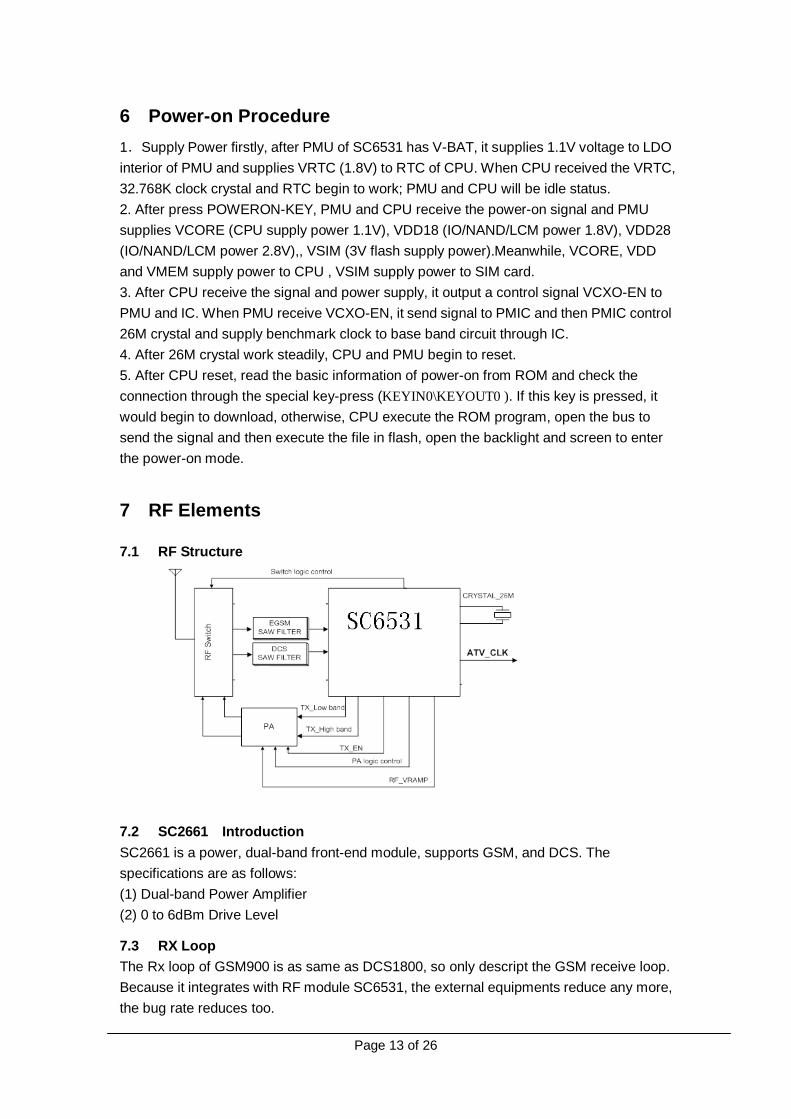
7.1 RF Structure
7.2 SC2661 Introduction SC2661 is a power, dual-band front-end module, supports GSM, and DCS. The specifications are as follows: (1) Dual-band Power Amplifier (2) 0 to 6dBm Drive Level
7.3 RX Loop The Rx loop of GSM900 is as same as DCS1800, so only descript the GSM receive loop. Because it integrates with RF module SC6531, the external equipments reduce any more, the bug rate reduces too.
Page 14 of 26
The RX signal runs to SC6531 RF from antenna switch 、SAW FILTER through matched circuit. The SC6531 choose GSM900 under control signal and divided the RX/TX signals through filter. The signal input to SC6531 through matched circuit, blow up low-noise→ mixing→ band-pass filter→ intermediate frequency blow up → mixing→ filter → I/O output.
7.4 TX Loop Four I/Q signals input → I/Q modulation→ mixing → PA amplifier output → Antenna switch →Antenna transmit
7.5 RF FAQ The main problem of RF is BT failure. The PCBA BT is Board Test, makes up of two parts as battery calibration and RF calibration. The battery calibration main adjust the coefficient between phone and battery to display voltage of battery and voltage output. RF calibration main adjust the RF parameter to accord with the GSM criterion. The battery calibration failure usually includes the voltage of battery charging and current calibration: The maintenance method is that, check the setup of calibration tool and NV firstly; and then check the connection of clamping and PCBA. It has no problem, it maybe the base chip U100 emptily or cold soldering, please soldered again or replace to solve it. The RF calibration failure usually is frequency calibration, includes GSM, DCS, PCS TX calibration. The error happen during calibrate AFC circuit; calibrate the frequency through RF chain. So it is caused by RF chain mainly. You can open the software to check the RF chain, usually the soldering of SW1 and U301 has problems, solder again or replace them to solve it. If the RF chain has no problem, please check X100 (26MHz crystal), please replace or solder it again. If GSM, DCS, PCS TX frequency calibrate error, it maybe U301 emptily soldering, please solder them again.
7.6 BUG Analysis Coupling Power too Low: If the single PCBA connection tests pass, but after assembled, found the signal is too bad. The coupling power is too low during coupling test. This problem due to these cases as follows. ① TEST-PORT is emptily soldering; ② TEST-PORT is a bad one; ③ The spring of antenna assembled badly or distortion, cannot connect the soldering pad of antenna on PCB.
Page 15 of 26
8 Trouble & Service
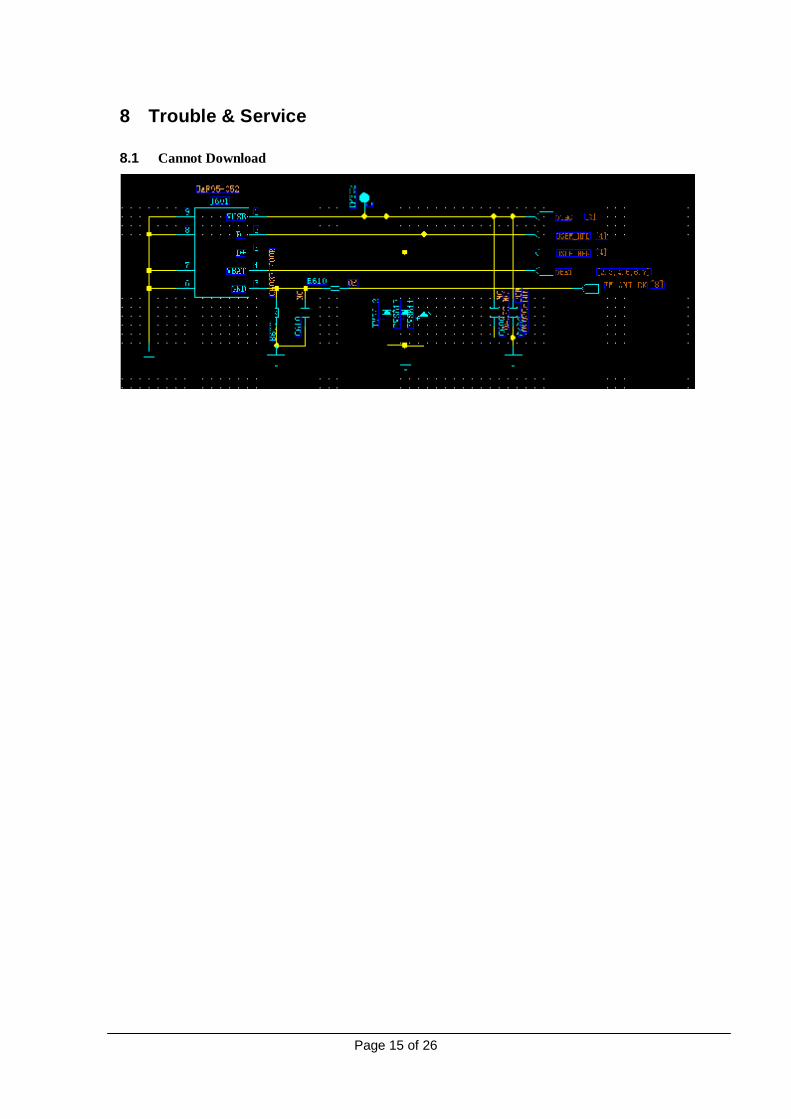
8.1 Cannot Download
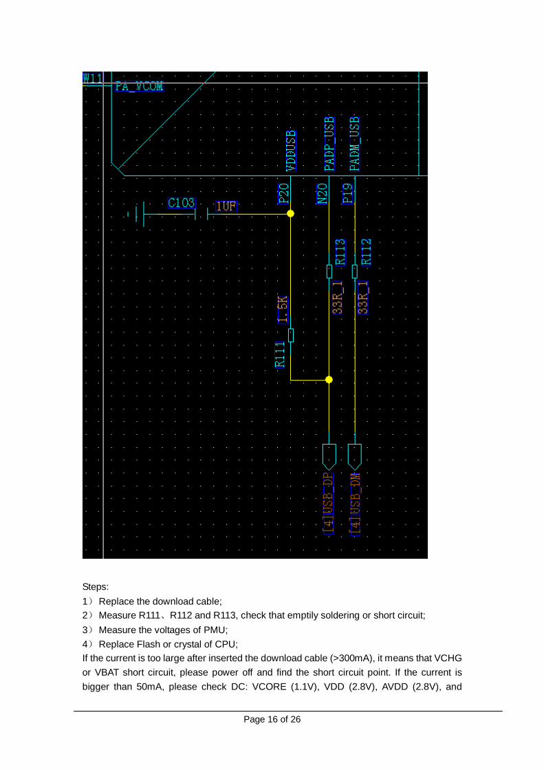
Page 16 of 26
Steps: 1) Replace the download cable; 2) Measure R111、R112 and R113, check that emptily soldering or short circuit; 3) Measure the voltages of PMU; 4) Replace Flash or crystal of CPU; If the current is too large after inserted the download cable (>300mA), it means that VCHG or VBAT short circuit, please power off and find the short circuit point. If the current is bigger than 50mA, please check DC: VCORE (1.1V), VDD (2.8V), AVDD (2.8V), and
Page 17 of 26
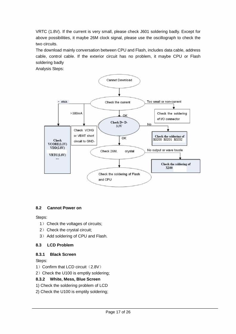
VRTC (1.8V). If the current is very small, please check J601 soldering badly. Except for above possibilities, it maybe 26M clock signal, please use the oscillograph to check the two circuits. The download mainly conversation between CPU and Flash, includes data cable, address cable, control cable. If the exterior circuit has no problem, it maybe CPU or Flash soldering badly Analysis Steps:
8.2 Cannot Power on
Steps: 1) Check the voltages of circuits; 2) Check the crystal circuit; 3) Add soldering of CPU and Flash.
8.3 LCD Problem
8.3.1 Black Screen Steps: 1)Confirm that LCD circuit(2.8V) 2)Check the U100 is emptily soldering; 8.3.2 White, Mess, Blue Screen 1) Check the soldering problem of LCD 2) Check the U100 is emptily soldering;
Page 18 of 26
8.4 Keypad Invalid
Steps: 1)Measure the col cable of connector and row cable resistance to GND by multimeter, check short circuit 2)If it is short circuit, check the soldering tin and measure it by multimeter 3)If not short circuit but high-resistance status, check the keypad connector is emptily soldering 4)If it is still fail, please check CPU is emptily soldering
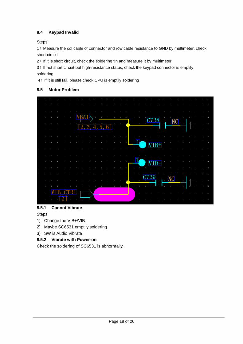
8.5 Motor Problem
8.5.1 Cannot Vibrate Steps: 1) Change the VIB+/VIB- 2) Maybe SC6531 emptily soldering 3) SW is Audio Vibrate 8.5.2 Vibrate with Power-on Check the soldering of SC6531 is abnormally.
Page 19 of 26
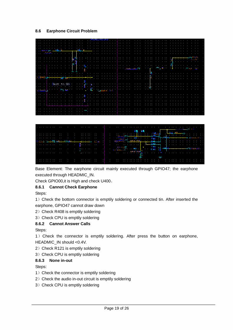
8.6 Earphone Circuit Problem
Base Element: The earphone circuit mainly executed through GPIO47; the earphone executed through HEADMIC_IN. Check GPIO00,it is High and check U400。 8.6.1 Cannot Check Earphone Steps: 1)Check the bottom connector is emptily soldering or connected tin. After inserted the earphone, GPIO47 cannot draw down 2)Check R408 is emptily soldering 3)Check CPU is emptily soldering 8.6.2 Cannot Answer Calls Steps: 1)Check the connector is emptily soldering. After press the button on earphone, HEADMIC_IN should <0.4V. 2)Check R121 is emptily soldering 3)Check CPU is emptily soldering 8.6.3 None in-out Steps: 1)Check the connector is emptily soldering 2)Check the audio in-out circuit is emptily soldering 3)Check CPU is emptily soldering
Page 20 of 26
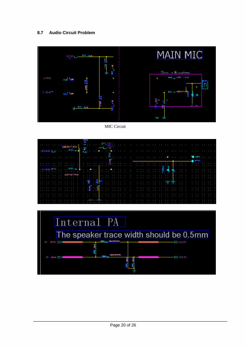
8.7 Audio Circuit Problem
MIC Circuit
Page 21 of 26
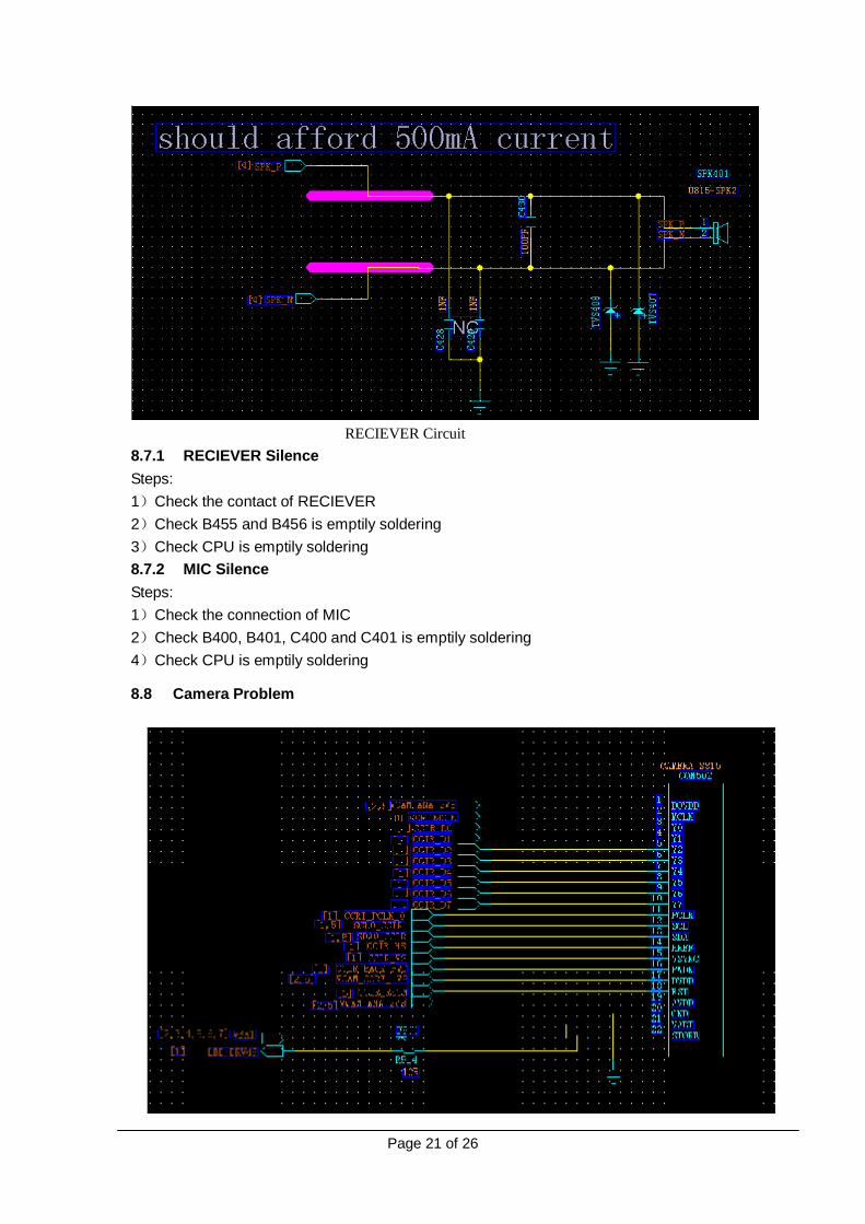
RECIEVER Circuit 8.7.1 RECIEVER Silence Steps: 1)Check the contact of RECIEVER 2)Check B455 and B456 is emptily soldering 3)Check CPU is emptily soldering 8.7.2 MIC Silence Steps: 1)Check the connection of MIC 2)Check B400, B401, C400 and C401 is emptily soldering 4)Check CPU is emptily soldering
8.8 Camera Problem
Page 22 of 26
8.8.1 Not Ready Steps: 1)Check the CAMERA connector is emptily soldering 2)Check the power manager chip is emptily soldering 3)Check CPU is emptily soldering 8.8.2 Mess Screen Steps: 1)Check the connector is emptily soldering 2)Check CPU is emptily soldering
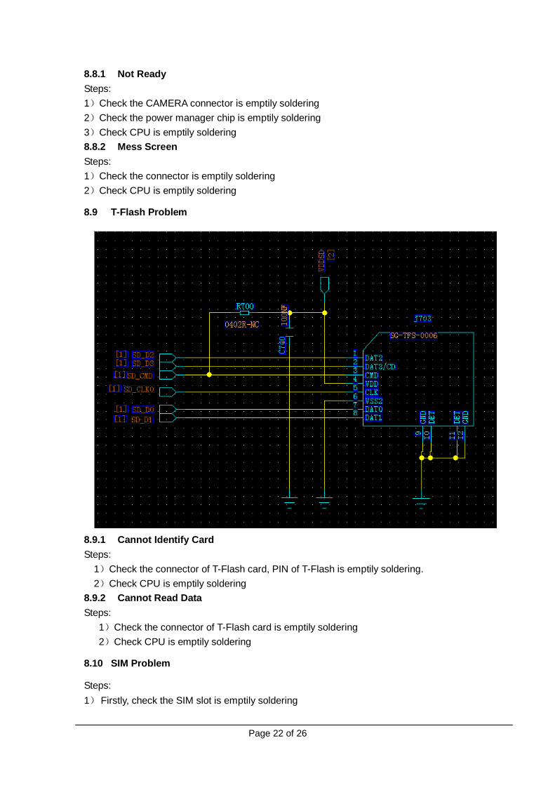
8.9 T-Flash Problem
8.9.1 Cannot Identify Card Steps:
1)Check the connector of T-Flash card, PIN of T-Flash is emptily soldering. 2)Check CPU is emptily soldering
8.9.2 Cannot Read Data Steps: 1)Check the connector of T-Flash card is emptily soldering 2)Check CPU is emptily soldering
8.10 SIM Problem
Steps: 1) Firstly, check the SIM slot is emptily soldering
Page 23 of 26
2) Add soldering PMU chip and CPU
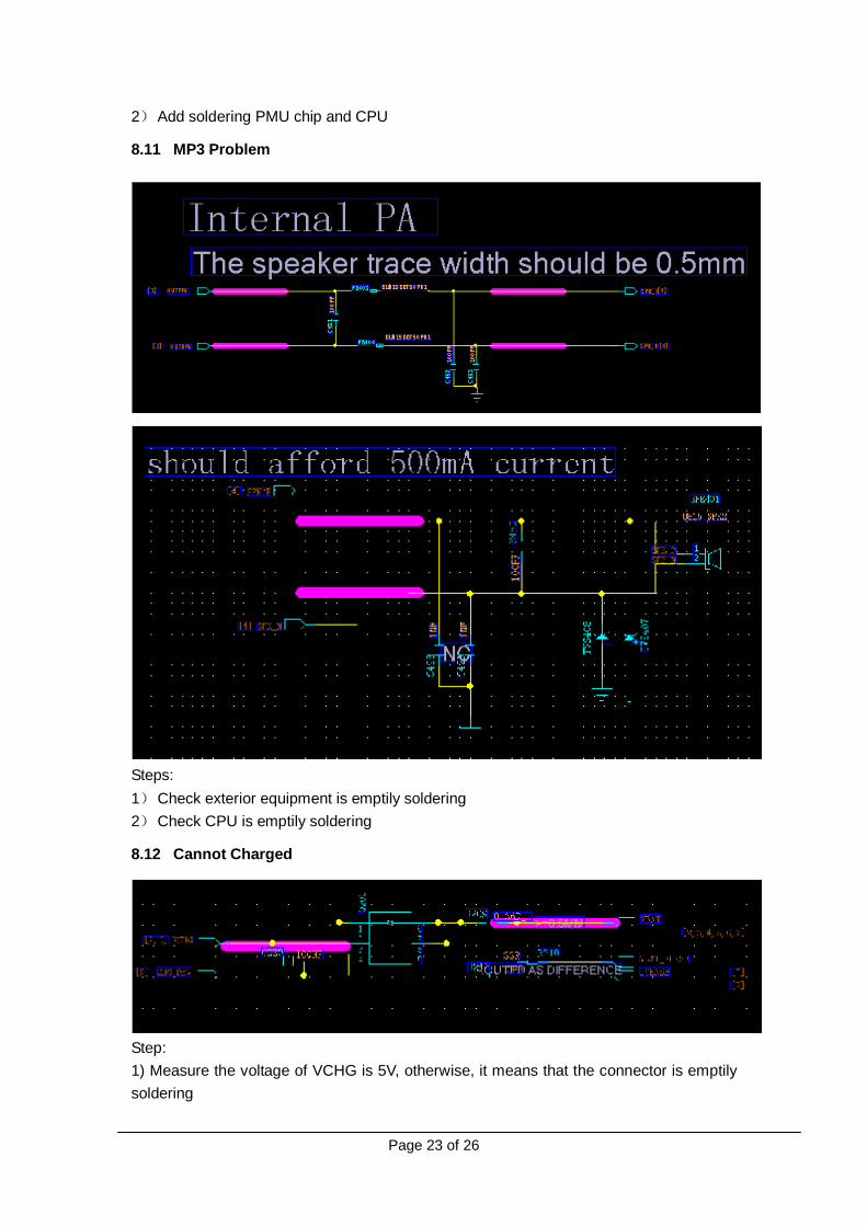
8.11 MP3 Problem
Steps: 1) Check exterior equipment is emptily soldering 2) Check CPU is emptily soldering
8.12 Cannot Charged
Step: 1) Measure the voltage of VCHG is 5V, otherwise, it means that the connector is emptily soldering
Page 24 of 26
2)Check Q200 chip is emptily soldering
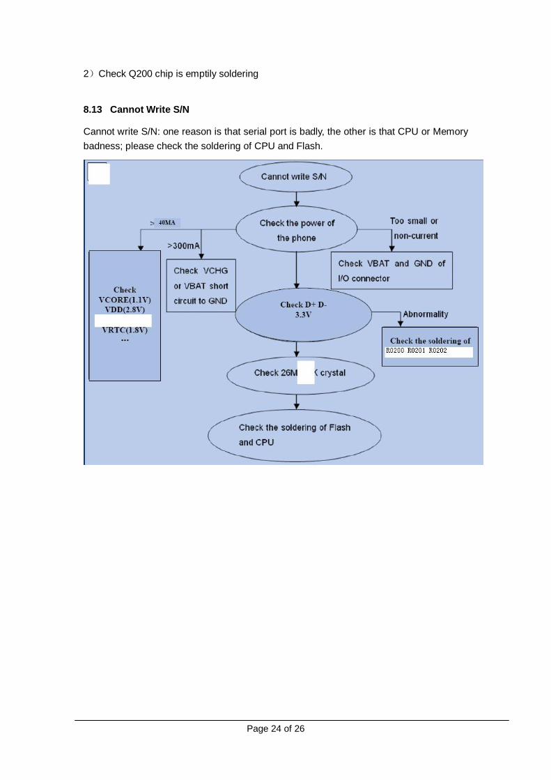
8.13 Cannot Write S/N
Cannot write S/N: one reason is that serial port is badly, the other is that CPU or Memory badness; please check the soldering of CPU and Flash.
Page 25 of 26
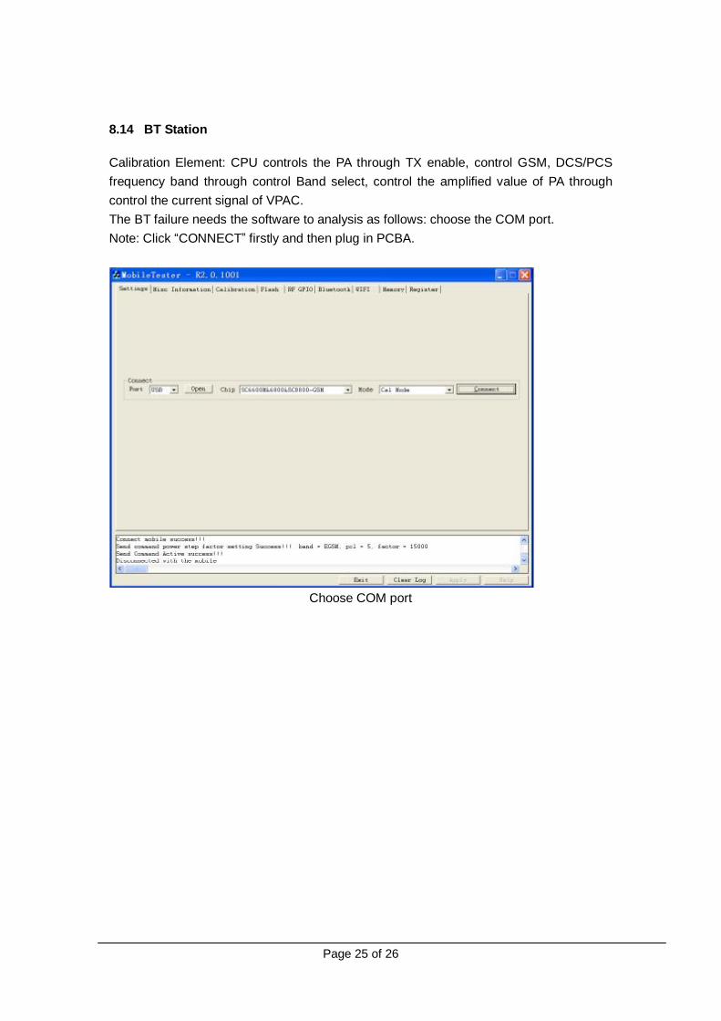
8.14 BT Station
Calibration Element: CPU controls the PA through TX enable, control GSM, DCS/PCS frequency band through control Band select, control the amplified value of PA through control the current signal of VPAC. The BT failure needs the software to analysis as follows: choose the COM port. Note: Click “CONNECT” firstly and then plug in PCBA.
Choose COM port
Page 26 of 26