Embed Size (px)
Citation preview
5
Fabrication, Doping and Characterization of Polyaniline and Metal Oxides:
Dye Sensitized Solar Cells
Sadia Ameen1, M. Shaheer Akhtar2, Young Soon Kim1 and Hyung-Shik Shin1
1Energy Materials & Surface Science Laboratory, Solar Energy Research Center, School of Chemical Engineering, Chonbuk National University, Jeonju,
2New & Renewable Energy Material Development Center (NewREC), Chonbuk National University, Jeonbuk,
Republic of Korea
1. Introduction
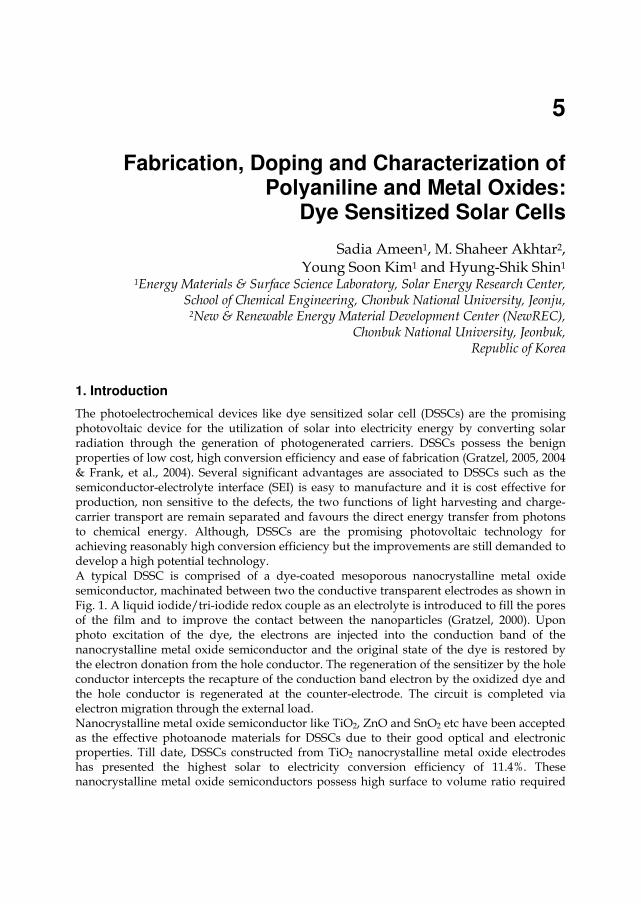
The photoelectrochemical devices like dye sensitized solar cell (DSSCs) are the promising photovoltaic device for the utilization of solar into electricity energy by converting solar radiation through the generation of photogenerated carriers. DSSCs possess the benign properties of low cost, high conversion efficiency and ease of fabrication (Gratzel, 2005, 2004 & Frank, et al., 2004). Several significant advantages are associated to DSSCs such as the semiconductor-electrolyte interface (SEI) is easy to manufacture and it is cost effective for production, non sensitive to the defects, the two functions of light harvesting and charge-carrier transport are remain separated and favours the direct energy transfer from photons to chemical energy. Although, DSSCs are the promising photovoltaic technology for achieving reasonably high conversion efficiency but the improvements are still demanded to develop a high potential technology. A typical DSSC is comprised of a dye-coated mesoporous nanocrystalline metal oxide semiconductor, machinated between two the conductive transparent electrodes as shown in Fig. 1. A liquid iodide/tri-iodide redox couple as an electrolyte is introduced to fill the pores of the film and to improve the contact between the nanoparticles (Gratzel, 2000). Upon photo excitation of the dye, the electrons are injected into the conduction band of the nanocrystalline metal oxide semiconductor and the original state of the dye is restored by the electron donation from the hole conductor. The regeneration of the sensitizer by the hole conductor intercepts the recapture of the conduction band electron by the oxidized dye and the hole conductor is regenerated at the counter-electrode. The circuit is completed via electron migration through the external load. Nanocrystalline metal oxide semiconductor like TiO2, ZnO and SnO2 etc have been accepted as the effective photoanode materials for DSSCs due to their good optical and electronic properties. Till date, DSSCs constructed from TiO2 nanocrystalline metal oxide electrodes has presented the highest solar to electricity conversion efficiency of 11.4%. These nanocrystalline metal oxide semiconductors possess high surface to volume ratio required
www.intechopen.com
Solar Cells – Dye-Sensitized Devices
96
Fig. 1. Mechanistic diagram of dye sensitized solar cell under light illumination.
for the high absorption of dye molecules for the improved light harvesting efficiency but the
challenges like enhancement in the electron transport rate, reduction of recombination rate
and the improvement in the energy conversion efficiency are still associated with metal
oxide semiconductor based DSSCs. It has been reported that the photoelectrodes made of
metal oxides nanostructures like nanoparticles, nanorods, nanowires and nanotubes
improve the photovoltaic properties of DSSCs such as JSC, VOC, FF and conversion efficiency
by the effective electron transfer during the performance of DSSCs. The conducting
polymers are the semiconducting polymers which exhibit good electrical properties similar
to metals and possess unique properties like light weight, resistance to corrosion, flexibility
and low cost. The nanostructures of conducting polymers are excessively exploited in the
electronic devices due to the large surface area of the nanomaterials and their unique
electronic properties (Huang et al., 2006, Zhnag et al., 2006, Wan, 2008, 2009 & Li et al.,
2009). These perspectives have prompted the researchers for the rapid development of
conducting polymers and the nanocrystalline metal oxide semiconductors for improving the
processability, functionality and the conversion efficiency of DSSCs.
In this chapter, we have briefly surveyed the conducting polymers, its doping and the different morphologies of nanocrystalline metal oxide semiconductors for the effective processing, functionality and the fabrication of DSSCs. The chapter focuses the recent developments in the heterostructures diodes, Ohmic devices and DSSCs fabricated with polyaniline (PANI) and the nanostructured metal oxides. The morphology, structure and physiochemical properties of TiO2 and ZnO nanostructure semiconductors have been reviewed as photoelectrode for the application of DSSCs. It has been reviewed that the performances of DSSCs are considerably affected by the preparation, morphology and the electrical properties of conducting polymers and metal oxide semiconductors. TiO2 and ZnO nanostructures based photoelectrodes have shown comparable photovoltaic performance compared to the conventional TiO2 nanoparticles based DSSCs. On the other hand, the conducting polymers as a hole transport materials are found as the potential candidates for
www.intechopen.com

Fabrication, Doping and Characterization of Polyaniline and Metal Oxides: Dye Sensitized Solar Cells
97
replacing the liquid electrolyte in DSSCs and the dopants have been discussed for enhancing the conducting properties of a particular polymer i.e. PANI.
2. Aspects of conducting polymers
The polymers are insulators due to the covalent bonded atoms in the polymer chain and thus, there is no scope for the delocalization of the valence electrons and consequently neither charge carriers nor the path for their movement are available (Stejskal et al., 2002). However, the important classes of polymers called as conducting polymers are semiconductors (Friend et al., 1999) and their band gaps could be tuned by alternating the chemical nature of either the polymer backbone or the side groups present in the polymeric chain. The overlapping of the molecular orbital for the formation of the delocalized molecular wave functions and secondly the partially filled molecular orbital for a free movement of electrons throughout the polymeric structure are the basic requirements for the polymers to become conducting in nature. These conducting polymers exhibit the unusual electronic properties such as electrical conductivity, low energy optical transitions, low ionization potential and high electron affinity (Park et al., 2010) due to the presence of extended π-conjugated systems along the polymeric chain (Gerard et al., 2002). The electrical properties of the conducting polymers could be easily tuned from insulating to metallic range by the reversible chemical, electrochemical and physical properties controlled by a doping/de-doping procedure. The electrical properties are changed by the partial oxidation or reduction of the polymer chain during the doping procedure. The conducting polymers possess the appended advantage of tailor-made property for accomplishing the requirements of the particular application through the modifications in the polymer structure. It is reported that the nanostructures of conducting polymer not only retain these unique characteristics, but also exhibit the properties like large surface area, size, and quantum effect etc which are important for designing and making the novel photovoltaic devices (Xia et al., 2010). Out of several conducting polymers, polyaniline (PANI) is the centre of scientific interest and has been considered as one of the most potential conducting polymers. The interest in PANI could possibly be linked to the numerous applications for various electrochemical, electro rheological and in the electronic fields such as batteries, sensors, controlling systems and organic displays (Smith, 1998, Wessling, 2001, Cho et al., 2002 & Choi et al. 2001) because of its facile synthetic process, good environmental stability, easy conductivity control and cheap production in large quantities. The high yield of PANI demands several essential conditions such as highly pured monomers, chemicals and solvents for obtaining the high quality polymer, the strict control on the polymerization conditions, inert and dry environment for the polymerization since the small variation in the polymerization conditions might alter the nature of the product, and as PANI might undergo isomerization reaction under light and heat therefore, the synthesized PANI products should be kept in a dark, cool and dry place (Ameen, et al., 2010)
3. General approaches for the synthesis of PANI
3.1 Interfacial polymerization In a typical reaction (Huang, et al., 2003, Virji, et al., 2004, King, et al., 2005 & Huang et al., 2004) aniline monomer is dissolved into the organic solvents which have either low or high density than water like hexane, benzene, toluene, carbon tetrachloride, chloroform etc. A
www.intechopen.com

Solar Cells – Dye-Sensitized Devices
98
separate aqueous solution of ammonium peroxydisulphate (APS) as an oxidant is prepared with the acids such as HCl, sulfuric acid, CSA, toluene sulfonic acid etc. The two solutions are then gently transferred to a glass vial for the generating the interface between the two layers. As the reaction proceeds, the green colored PANI is formed at the interface and gradually migrates into the aqueous phase and slowly the entire aqueous phase get filled homogeneously with dark-green PANI. The aqueous phase is collected through filtration after 24 h. The non-conducting PANI could be obtained by dialyzing the synthesized PANI with ammonia solution
3.2 Rapid mixing of reactants This is the simplest method for synthesizing PANI and in place of conventionally slow addition of the aqueous APS solution, the aniline monomer is mixed rapidly with APS solution. Here, the initiator molecules are consumed rapidly after the initialization of the polymerization reaction due to the even distribution of aniline monomer and APS molecules in the solution.
3.3 Sonochemical synthesis Jing et al (Jing, et al., 2006, 2007) has reported the synthesis of PANI similar to the synthesis procedure of conventional PANI. The acidic APS solution is added dropwise to an acidic aniline solution, and subjected to the ultrasonic irradiation which results to the high yield of PANI. It has been found that the excessive addition of aniline monomer or APS could contribute to the continuous formation of the primary PANI products or could lead the agglomeration of PANI. Unlike conventional procedure where irregular morphology of PANI is obtained, the sonochemical synthesis strictly prevents the further growth and agglomeration and thus, generates uniform morphology of PANI.
3.4 Electrophoretic synthesis The first step of a reaction requires a preparation of conducting PANI through the chemical
procedure using APS as oxidant. In the second step, a stock solution of PANI (1 mg/ml) is
prepared in the formic acid and the colloidal suspension is prepared by adding 100 ml of the
stock solution into acetonitrile for the preparation of an electrolyte. In the colloidal
suspension, PANI dissociate into ions due to high dielectric medium which is offered by
acetonitrile and thus, results to the formation of the positively charged PANI. The last step
involves the electrophoretic film deposition where under the influence of applied voltage for
a required time duration, positively charged colloid spheres of PANI in acidic colloidal
suspension starts moving towards the negatively biased fluorinated tin oxide glass (FTO)
electrode. This stepwise growth synthesis produces the uniform nanostructures of PANI on
the surfaces of the FTO glass substrates.
3.5 Plasma polymerization The plasma polymerization, as shown in Fig. 2 requires four parts (1) a reactor chamber quartz tube (2 cm), (2) Cu coil (4 in.), (3) plasma system (R.F. generator: 0-600 W, matching network frequency of 13.56 MHz) and (4) mechanical vacuum pump (speed 600 1/min). The glow discharges are introduced through RF amplifier with a resistive coupling mechanism at 13.5 MHz and power of 120 W. These discharges are set without carrier gas or any other additional chemical elements to prevent the contamination. The cleaned FTO glass
www.intechopen.com

Fabrication, Doping and Characterization of Polyaniline and Metal Oxides: Dye Sensitized Solar Cells
99
substrates are placed just below the RF coil, placed inside the quartz tube. Initially, the chamber is evacuated to a base pressure of 10-3 Torr through a rotator vacuum pump. After attaining the base pressure, aniline monomer is injected, using a hypodermic syringe and the reaction is promoted by the collisions of the aniline monomer molecules with the ions/particles present in the plasma.
Fig. 2. Reactor setup for plasma synthesis of PANI. Reprinted with permission from [Ameen S. et al 2009], Superlatt. Microstruc. 46 (2009) 745. © 2009, Elsevier Ltd.
4. Concept of doping in PANI
Doping is the unique, central, underlying and unifying concept, which distinguishes PANI as conducting polymer from other insulating polymers. The controlled addition of known chemical species results in the dramatic changes in the electronic, electrical, magnetic, optical and structural properties of PANI. The doping procedures of inorganic semiconductors and for conducting polymers including PANI are fundamentally different from each other. In PANI, the dopant concentrations are exceptionally high compared to commonly doped inorganic semiconductors (typically in parts per million ranges) and the doping of PANI involves random dispersion or aggregation of dopants in molar concentrations in the disordered structure of entangled chains and fibrils. However, for inorganic semiconductors, the doping generates either holes in the valence band or electrons in the conduction band. The doping of PANI generates high conductivity primarily by increasing the carrier concentrations and leads to the conjugational defect like solitons, polarons, bipolarons in the polymer chain. Doping is a reversible produce which could be carried out chemically or electrochemically with the oxidation or reduction by accepting or donating the electrons respectively and thus, results to the positive or negative charges. Ameen et al have used various acids and binary mixtures as dopants to improve the electrical conductivity of PANI.
4.1 Doping with sulfamic acid Sulfamic acid is one of the promising dopant which displays the properties of handling ease, solubility, and low corrosiveness. It is a dry, non-volatile stable solid acid, which is moderately soluble in water at room temperature. Wadia et al prepared the thin film of sulfamic acid doped PANI as electrochemical sensor for the determination of nitrite (Dhaoui, et al., 2007, 2008). Ameen et al reported the electrical conductivity of PANI nanostructures in the range of 1.1×10⁻⁴ – 4.50×10⁻³ohm-1cm-1, doped with different wt% of sulfamic acid (Ameen, et al., 2007). Moreover, PANI nanofibers doped with sulfamic acid thin film was applied as counter electrodes for the fabrication of DSSCs and obtained the conductivity of 2.06×10⁻⁴ ohm-1cm-1 by Ameen et al (Ameen, et al., 2010).
www.intechopen.com
Solar Cells – Dye-Sensitized Devices
100
4.2 Doping with sodium thiosulphate Sodium thiosulphate is an odorless translucent crystals or white crystalline powder which is soluble in water and exhibit the stability. It is incompatible with strong acid and is not hazardous. Ameen et al reported the electrical conductivity of PANI nanostructures in the range of 8.55×10⁻⁹ – 3.67×10⁻⁷ ohm-1cm-1 after doping with sodium thiosulphate (Ameen, et al., 2009).
4.3 Doping with samarium (III) chloride Samarium (III) chloride is a light yellow colored strong Lewis acid. This dopant is non hazardous and stable in nature and is reported to increase the conductivity of PANI nanostructure from 3.70×10⁻¹¹ to1.30×10−9 ohm-1cm-1 (Ameen, et al., 2009).
4.4 Doping with praseodymium (III) chloride Praseodymium (III) Chloride is a green colored powder which does not show thermal decomposition and is stable in nature. It is an excellent water-soluble crystalline strong Lewis acid and after doping is reported to show the conductivity of PANI nanostructures in the range 1.87×10⁻¹¹ – 2.22×10⁻¹⁰ohm-1cm-1 (Ameen, et al., 2008).
4.5 Doping with binary dopant: ZrO2/AgI & ZrO2/PbI2 In this binary dopant mixture ZrO2 is a luminescent material which usually makes no contribution in the conductivity of PANI. On the other hand, AgI is a non luminescent material which enhances the conductivity of PANI. The binary effects of these two materials have improved the optical and the electrical conductivity of PANI nanostructures in the range of 9.28×10⁻¹⁰ – 3.763×10⁻⁶ ohm-1cm-1(Ameen, et al., 2007). Shaoxu et al reported the synthesis, characterization and the thermal analysis of PANI-ZrO2 nanocomposites (Wang, et al., 2006). The increased ZrO2 concentration in the binary dopant mixture exhibits a high PL emission intensity which improves optoelectronic properties of PANI. Ameen et al reported the effect of ZrO2/PbI2 doping on the electrical properties of PANI and the conductivity improves from 2.70×10⁻¹³ to 8.81×10⁻⁴ ohm-1cm-1(Ameen, et al., 2009).
5. Applications of PANI in heterostructure devices
5.1 Electrophoretic deposition of PANI for heterostructure devices 5.1.1 Electrophoretically deposited PANI/ZnO heterostructure diodes The fabrication of inorganic/organic heterostructure diodes is reported by the electrophoretic process for depositing organic materials (PANI, p-type) film on inorganic n-type ZnO NPs thin film substrate with top Pt thin layer contact by Ameen et al (Ameen, et al., 2009). The pristine ZnO film is composed of well crystalline ZnO nanoparticles of size ~50-70 nm, shown in Fig. 3 (a). The penetration of the PANI molecules into the crystalline ZnO NPs thin film upon electrophoretic deposition display the accumulation of ZnO NPs and thus, the size of ZnO nanoparticles get increased to ~90 nm (Fig. 3 (b)). This assemblage confirms the substantive interaction and incorporation of electrophoretic deposited PANI into the crystalline ZnO nanoparticles thin film substrates. The FTIR studies (Fig. 4 (I)) shows the considerable shifting of the peaks might due to the bonding between the hydroxyl groups and the imine groups of the PANI molecules. Noticeably, the UV-visible spectra of PANI/ZnO thin film (Fig. 4 (II)) shows that the peak (a) retains its position, considerable large blue shift for peak (b) is noticed and small red shift
www.intechopen.com

Fabrication, Doping and Characterization of Polyaniline and Metal Oxides: Dye Sensitized Solar Cells
101
Fig. 3. Surface FE-SEM images of (a) synthesized ZnO nanoparticles (b) electrophoretically deposited PANI/ZnO thin film. Reprinted with permission from [Ameen S. et al, 2009],
Superlatt. Microstruc. 46 (2009) 872. 2009, Elsevier Ltd.
Fig. 4. (I): Typical FTIR spectrum of (a) pristine PANI (b) ZnO nanoparticles and (c) electrophoretically deposited PANI/ZnO thin film. (II): UV-Vis spectra of pristine PANI and electrophoretically deposited PANI/ZnO thin film. Inset shows the UV-Vis spectrum of ZnO nanoparticles. Reprinted with permission from [Ameen S., 2009], Superlatt. Microstruc.
46 (2009) 872. 2009, Elsevier Ltd.
www.intechopen.com
Solar Cells – Dye-Sensitized Devices
102
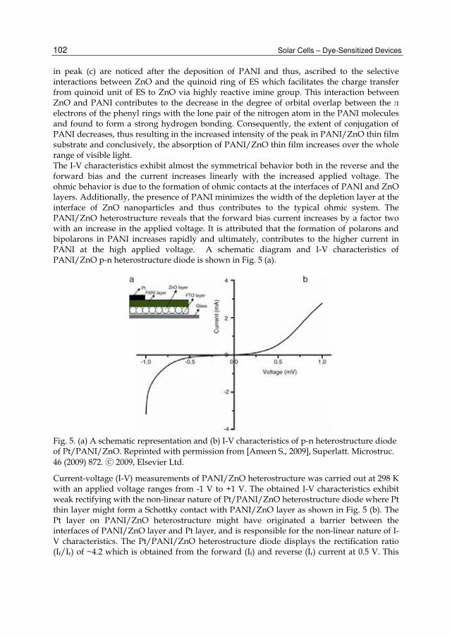
in peak (c) are noticed after the deposition of PANI and thus, ascribed to the selective interactions between ZnO and the quinoid ring of ES which facilitates the charge transfer from quinoid unit of ES to ZnO via highly reactive imine group. This interaction between ZnO and PANI contributes to the decrease in the degree of orbital overlap between the л electrons of the phenyl rings with the lone pair of the nitrogen atom in the PANI molecules and found to form a strong hydrogen bonding. Consequently, the extent of conjugation of PANI decreases, thus resulting in the increased intensity of the peak in PANI/ZnO thin film substrate and conclusively, the absorption of PANI/ZnO thin film increases over the whole range of visible light. The I-V characteristics exhibit almost the symmetrical behavior both in the reverse and the forward bias and the current increases linearly with the increased applied voltage. The ohmic behavior is due to the formation of ohmic contacts at the interfaces of PANI and ZnO layers. Additionally, the presence of PANI minimizes the width of the depletion layer at the interface of ZnO nanoparticles and thus contributes to the typical ohmic system. The PANI/ZnO heterostructure reveals that the forward bias current increases by a factor two with an increase in the applied voltage. It is attributed that the formation of polarons and bipolarons in PANI increases rapidly and ultimately, contributes to the higher current in PANI at the high applied voltage. A schematic diagram and I-V characteristics of PANI/ZnO p-n heterostructure diode is shown in Fig. 5 (a).
Fig. 5. (a) A schematic representation and (b) I-V characteristics of p-n heterostructure diode of Pt/PANI/ZnO. Reprinted with permission from [Ameen S., 2009], Superlatt. Microstruc.
46 (2009) 872. 2009, Elsevier Ltd.
Current-voltage (I-V) measurements of PANI/ZnO heterostructure was carried out at 298 K with an applied voltage ranges from -1 V to +1 V. The obtained I-V characteristics exhibit weak rectifying with the non-linear nature of Pt/PANI/ZnO heterostructure diode where Pt thin layer might form a Schottky contact with PANI/ZnO layer as shown in Fig. 5 (b). The Pt layer on PANI/ZnO heterostructure might have originated a barrier between the interfaces of PANI/ZnO layer and Pt layer, and is responsible for the non-linear nature of I-V characteristics. The Pt/PANI/ZnO heterostructure diode displays the rectification ratio (If/Ir) of ~4.2 which is obtained from the forward (If) and reverse (Ir) current at 0.5 V. This
www.intechopen.com

Fabrication, Doping and Characterization of Polyaniline and Metal Oxides: Dye Sensitized Solar Cells
103
low If/Ir value indicates that the PANI/ZnO heterostructure exhibits a weak rectifying nature and attains low turn-on voltage of ~0.15 V and delivers reasonably high current of ~0.08 mA with broader breakdown voltage (~0.52 V) with very high leakage current of ~0.6 mA.
5.1.2 Electrophoretically deposited PANI/TiO2 heterostructure diodes PANI has been electrophoretically deposited (EPD) on the surface of TiO2 nanoparticulate thin film for the fabrication of heterostructure devices by Ameen et al (Ameen, et al., 2011). The enhancements in the electron transport and current density have been explained in terms of the increased charge carriers mobility with improved optical absorption by the heterostucture diodes. Fig. 6 (a) shows the morphology of well crystalline TiO2 nanoparticles thin film of size ~20–25 nm. However, upon EPD, the size of TiO2 nanoparticles increased to ~70–80 nm (Fig. 6 (b)) might due to the penetration of PANI molecules into the pores of mesoporous TiO2 nanoparticulate thin film. Additionally, the uniform deposition and the penetration of PANI on TiO2 nanoparticulate thin film could be seen in the Fig. 6 (c).
Fig. 6. Surface FESEM images of (a) TiO2 nanoparticles (b) electrophoretically deposited PANI/TiO2 nanoparticulate thin film and (c) cross-section image of electrophoretically deposited PANI/TiO2 nanoparticulate thin film. Reprinted with permission from [Ameen S.,
2011], J. Nanosci. Nanotech. 11 (2011) 1559. 2011, American Scientific Publishers.
The shifting of FTIR peaks, as shown in Fig. 7 (a) indicates the existence of the hydrogen bonding between the surface hydroxyl groups of TiO2 nanoparticles and the imine groups of PANI molecules (Somani, et al., 1999 & Nivetal, et al., 2003). The UV-Vis spectra of pristine PANI and PANI/TiO2 nanoparticulate thin film is shown in (Fig. 7 (b)). The pristine PANI exhibits two characteristics bands at 331 and 625 nm which correspond to л–л* transitions of the phenyl rings of PANI and n-л* transitions respectively. In PANI/TiO2 nanoparticulate thin film substrates, the peak at 269 nm retains its position, while the bands at 625 nm and
www.intechopen.com
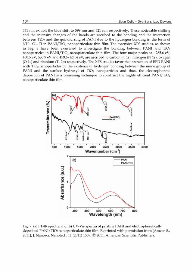
Solar Cells – Dye-Sensitized Devices
104
331 nm exhibit the blue shift to 599 nm and 321 nm respectively. These noticeable shifting and the intensity changes of the bands are ascribed to the bonding and the interaction between TiO2 and the quinoid ring of PANI due to the hydrogen bonding in the form of NH···O—Ti in PANI/TiO2 nanoparticulate thin film. The extensive XPS studies, as shown in Fig. 8 have been examined to investigate the bonding between PANI and TiO2 nanoparticles in PANI/TiO2 nanoparticulate thin film. The four major peaks at ∼285.6 eV, 400.5 eV, 530.9 eV and 459.6/465.4 eV, are ascribed to carbon (C 1s), nitrogen (N 1s), oxygen (O 1s) and titanium (Ti 2p) respectively. The XPS studies favor the interaction of EPD PANI with TiO2 nanoparticles by the existence of hydrogen bonding between the imine group of PANI and the surface hydroxyl of TiO2 nanoparticles and thus, the electrophoretic deposition of PANI is a promising technique to construct the highly efficient PANI/TiO2 nanoparticulate thin film.
Fig. 7. (a) FT-IR spectra and (b) UV-Vis spectra of pristine PANI and electrophoretically deposited PANI/TiO2 nanoparticulate thin film. Reprinted with permission from [Ameen S.,
2011], J. Nanosci. Nanotech. 11 (2011) 1559. 2011, American Scientific Publishers.
www.intechopen.com

Fabrication, Doping and Characterization of Polyaniline and Metal Oxides: Dye Sensitized Solar Cells
105
Fig. 8. (a) Resolved C1s, (b) N1s, (c) O1s and (d) Ti 2p XPS spectra of electrophoretically deposited PANI/TiO2 nanoparticulate thin film. Reprinted with permission from [Ameen S., 2011], J. Nanosci. Nanotech. 11 (2011) 1559. © 2011, American Scientific Publishers.
Fig. 9. Pt/PANI/TiO2 nanoparticulate diode. Insets show the schematic representation of the PANI/TiO2 nanoparticulate heterostructure diode. Reprinted with permission from
[Ameen S., 2011], J. Nanosci. Nanotech. 11 (2011) 1559. 2011, American Scientific Publishers.
The current–voltage (I–V) characteristics of EPD PANI/TiO2 nanoparticulate heterostructure was carried out at different temperatures (25-1500C) with an applied voltage
www.intechopen.com
Solar Cells – Dye-Sensitized Devices
106
ranges from −1V to +1V, as shown in Fig. 9. A schematic diagram of Pt/PANI/TiO2 nanoparticulate heterostructure diode is shown in the inset of Fig. 9. The I–V characteristic of Pt/PANI/TiO2 nanoparticulate heterostructure diode exhibits a rectifying and nonlinear behavior which might originate by the formation of schottky contact/barrier between Pt layer and EPD PANI/TiO2 layer in Pt/PANI/TiO2 nanoparticulate heterostructure diode. Moreover, the ratio of forward (If) and reverse current (Ir), called as rectification ratio (If/Ir) of the device is estimated as 7.0 at the bias voltage of 0.5 V. The If/Ir value indicates that the EPD PANI/TiO2 nanoparticulate heterostructure shows a weak rectifying nature. The EPD PANI/TiO2 heterostructure diode attains turn-on voltage of ~ 0.40 V and derives quite high current of ~0.25 mA at 298 K. A broader breakdown voltage (~0.51 V) and good leakage current of ~0.9 mA are achieved by Pt/PANI/TiO2 nanoparticulate heterostructure diode. The low turn on voltage and high leakage current might result from the generation of high density of minority charge carriers from EPD PANI to n-type TiO2. In a reverse bias, Pt/PANI/TiO2 nanoparticulate heterostructure diode shows slightly high break down voltage (~0.55 V) which could be explained by the hopping effect originated from the conjugated bonding of PANI and the geometry/ morphology of TiO2 nanoparticles. Therefore, the uniform and controlled thickness of PANI layer onto TiO2 nanoparticulates thin film substrate by the electrophoretic deposition provides the improved performance of the p–n heterostructure devices.
5.2 Plasma enhanced polymerization of PANI for heterostructure devices 5.2.1 Fabrication of PANI/TiO2 heterostructure device The formation of an inorganic/organic heterojunction structure by depositing the plasma polymerized PANI on n-type nanocrystalline titania (TiO2) thin film substrate has been reported by Ameen et al (Ameen, et al., 2009). Fig. 10 (a) demonstrates a porous TiO2 formed on the FTO substrates. The film is composed of the well crystalline TiO2 nanoparticles of size ~25 nm, as shown in Fig. 10 (c). It is seen in Fig. 10 (b) that the PANI molecules are well penetrated into the porous TiO2 thin film upon the plasma enhanced polymerization. The accumulation of TiO2 nanoparticles occurs after the deposition of PANI on the surface of TiO2 thin film, and could be seen in Fig. 10 (d). This assemblage confirms the internalization of plasma deposited PANI into porous TiO2 nanoparticles thin film substrates. The I-V characteristics for PANI/TiO2 heterojunction structure, as shown in our reported work (Ameen, et al., 2009,), indicates that no barrier is apparently present because the I-V characteristic curve is almost linear. The forward bias current increases with an increased applied voltage and have attained almost the linear curve. The proficient current in PANI/TiO2 is attributed to well penetration of PANI molecules into the pores of TiO2
nanoparticles layers which improves the degree of contact with TiO2 and thus decreases the series resistance of the cell while increasing the current. The efficient charge movement at the junction of PANI and TiO2 interfaces has made the heterojunction structure which behaves as a typical ohmic system. Moreover, in the reverse bias, the lower current is related to the decrease of the depletion layer because of the presence of the charge carriers at TiO2 nanoparticles thin film.
5.2.2 Plasma deposited PANI on single and bilayer of TiO2 thin film for the fabrication of PANI/TiO2 heterostructure diodes The organic/inorganic thin film is obtained by plasma enhanced p-type PANI deposited on the individual single and bilayer n-type TiO2 thin film electrodes for the fabrication of p-n
www.intechopen.com

Fabrication, Doping and Characterization of Polyaniline and Metal Oxides: Dye Sensitized Solar Cells
107
Fig. 10. Cross-sectioned FE-SEM images of (a) pristine TiO2 (b) Plasma enhanced deposited PANI/TiO2 thin film and surface FESEM images of (c) pristine TiO2 (d) Plasma enhanced deposited PANI/TiO2 thin film. Reprinted with permission from [Ameen S., 2009], Superlatt. Microstruc. 46 (2009) 745. © 2009, Elsevier Ltd.
heterostructure by Ameen et al (Ameen, et al., 2011). The single layer TiO2 electrode exhibits
non uniform and less penetration of PANI molecules by plasma enhanced polymerization
into the pores of TiO2 thin film. However, the extent of PANI deposition has drastically
enhanced by the additional layer of TiO2 on the single layered electrode due to the uniform
and well penetration of PANI into the pores of TiO2 nanoparticles.
The XPS characterizations suggest that the plasma polymerized PANI are interacted to TiO2
by the formation of hydrogen bonding between imine group of PANI and surface hydroxyl
of TiO2. UV-Vis of PANI/TiO2 thin film electrode exhibit the peaks at 324 nm corresponds to
л–л∗ transitions centered on the benzenoid and quinoid units. This peak appears with high
intensity in PANI/bilayer TiO2 thin film electrode which indicates the enhanced deposition
of PANI molecules on the surface of TiO2. It could be attributed that highly porous surface
of bilayer TiO2 thin film absorbs large amount of PANI than the single layered TiO2 thin
film, as described in previous report (Ameen, et al., 2011).
The fabricated p-n heterostructure devices are comprised of plasma polymerized PANI (p-type) deposited on the single and bilayerTiO2 thin film (n-type) coated on FTO glass substrates with a top Pt thin layer contact. The I-V curve of the fabricated PANI/single layer TiO2 device attains low turn-on voltage of ~ 0.4 V and delivers reasonably high current of ~ 0.08 mA at 298 K, as described in previous report (Ameen, et al., 2011). However, a breakdown voltage (~0.57 V) with high leakage current of ~0.6 mA is obtained by Pt/PANI/single layer TiO2
www.intechopen.com

Solar Cells – Dye-Sensitized Devices
108
heterostructure device. On comparison, Pt/PANI/bilayer TiO2 heterostructure device shows the lower turn on voltage and low breakdown voltage with high leakage current than single layer TiO2 based heterostructure device. Here, the second layer of TiO2 in PANI/bilayer TiO2 provides a highly porous surface for the high loading of PANI molecules during the plasma enhanced polymerization and thus, produces high density of the minority charge carriers to n-type TiO2 thin film layer and results to the high leakage current with small turn-on voltage and breakdown voltage. It is attributed that the additional TiO2 thin film layer might increase the n-type character of the device. On the other hand, both the devices exhibit slight high reverse break down voltage (~0.58 V in single layer TiO2 and ~0.5 V in bilayer TiO2) which could be understood by considering the molecular geometry of PANI chains and geometry/morphology of TiO2 nanoparticles deposited on the FTO substrates which likely generate the hopping effect. The current densities reported by Sadia et al in the forward bias are considerably better than the data reported elsewhere on PANI based or other conducting polymer based heterostructure device (Dhawale, et al., 2008, Nadarajah, et al., 2008 & Maeng, et al., 2008). Under light illumination, both the devices constitute the no current flowing condition i.e. called open circuit voltage condition (VOC) and the maximum current condition called short circuit current (JSC) at zero voltage condition. This phenomena is absent in I-V characteristics under dark condition, which means that the fabricated devices could absorb photons for the generation of current and having the photovoltaic behavior under light illumination and thus, Pt/PANI/bilayer TiO2 heterostructure device is reported to achieve high JSC (~0.32 mA) with low VOC (~0.343 V) as compared with Pt/PANI/single layer TiO2 heterostructure device (JSC = ~0.20 mA and VOC = ~0.462 V).
6. Applications of PANI in dye sensitized solar cells (DSSCs)
Organic solar cells have attracted considerable attention in recent years due to several advantages such as low cost, processing at low temperature, flexible and large area production etc (Thompson, et al., 2008, Gunes, et al., 2007 & Bundgoard, et al., 2007). Usually, the organic materials are not good in carrier transport and thus, the power conversion efficiency is limited by the low dissociation probability of excitons and the inefficient hopping carrier transport (Shaw, et al. 2008 & Sirringhaus, et al., 1999). Among various organic solar cells, polymer solar cells have demonstrated an impressive scale up on power conversion efficiency and improvement in lifetime. Right now a remarkable 8% power conversion efficiency has been reached at laboratory scale, 6–8% for normal and 3–4% for inverted configurations (Waldauf, et al., 2006, Steim, et al., 2010, 2008 & Ameri, et al., 2009). Still, much work must be done in order to overcome the main difficulties observed for the technology i.e. enhancement of efficiency and lifetime. Thus, the need for novel materials acting as acceptors and donors, and the understanding of the interplay between interfaces (electrodes, optical spaces) are currently under an intense investigation. Semiconductor oxides have been applied extensively like antireflection coatings and scattering layers (Lee, et al., 2008), as interfacial layers in organic solar cells (Steim, et al., 2010, 2008) and as part of the active constituents of the device acting as electron transport materials in and hybrid DSSCs (Cantu, et al., 2010, 2006, 2007, 2006,Valls, et al., 2010, 2009). The semiconductor nanostructures are therefore proposed to combine with the organic materials to provide not only a large interface area between organic and inorganic components for exciton dissociation but also a fast electron transport in semiconductors. Hybrid solar cells are a mixture of nanostructures of both organic and inorganic materials.
www.intechopen.com

Fabrication, Doping and Characterization of Polyaniline and Metal Oxides: Dye Sensitized Solar Cells
109
Therefore, they combine the unique properties of inorganic semiconductor nanoparticles with properties of organic/polymeric materials (Arici, et al., 2003). In addition to this, low cost synthesis, processability and versatile manufacturing of thin film devices make them attractive (Sariciftci, et al., 1992 & Yu, et al., 1995). Also, inorganic semiconductor nanoparticles might have high absorption coefficients and particle size induced tunability of the optical band-gap. Thus, the hybrid solar cell is becoming interesting and attractive in recent years.
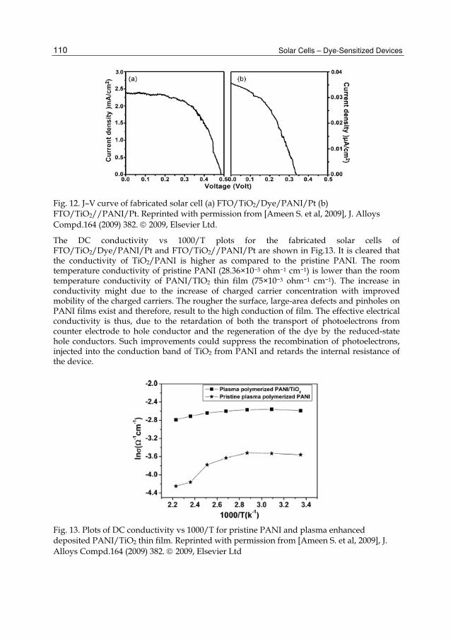
6.1 PANI/TiO2 thin film electrodes for the performance of DSSCs The TiO2/PANI and dye absorbed TiO2/PANI electrodes are prepared by plasma enhanced polymerization using aniline monomer for the fabrication of DSSCs by Ameen et al (Ameen, et al., 2009). The TiO2 thin film, prior to PANI deposition exhibits the particles of size ~20–25 nm, as shown in (Fig. 11 (b)). However, the proper attachment of plasma polymerized PANI on TiO2 thin film substrates (Fig. 11 (d)) and increases the size of TiO2 nanoparticles to ~50–60 nm indicate the effects of the penetration of PANI into TiO2 nanoparticles. The current density–voltage (J–V) performance of solar cell FTO/TiO2/Dye/PANI/Pt and FTO/TiO2/PANI/Pt are shown in Fig.12 respectively. The electric contact of the hole conductor and the pore filling extent of the hole conductor into the dye-sensitized TiO2 film are the two important factors which determine the photovoltaic behaviors of the devices. It has been found that the solar cell based on TiO2/Dye/PANI electrode executes great improvement in the overall conversion efficiency with the incorporation of dye layer on TiO2/PANI electrode and dramatically enhanced the photovoltaic properties such as open-circuit voltage (VOC), short-circuit current (JSC) and fill factor (FF) as compared to TiO2/PANI electrode based DSSC. These improvements are resulted from the formation of TiO2/PANI thin film, where the photon generated electrons could freely travel at the interface of the PANI and TiO2 without decay, and dissociate into free charge carriers effectively.
Fig. 11. (a) Cross-section and (b) surface view FESEM images of TiO2 deposited on FTO substrate. (c) and (d) show the cross-section and surface view FESEM images of Plasma enhanced deposited PANI/TiO2 film. Reprinted with permission from [Ameen S. et al, 2009], J. Alloys Compd.164 (2009) 382. © 2009, Elsevier Ltd.
www.intechopen.com
Solar Cells – Dye-Sensitized Devices
110
Fig. 12. J–V curve of fabricated solar cell (a) FTO/TiO2/Dye/PANI/Pt (b) FTO/TiO2//PANI/Pt. Reprinted with permission from [Ameen S. et al, 2009], J. Alloys
Compd.164 (2009) 382. 2009, Elsevier Ltd.
The DC conductivity vs 1000/T plots for the fabricated solar cells of FTO/TiO2/Dye/PANI/Pt and FTO/TiO2//PANI/Pt are shown in Fig.13. It is cleared that the conductivity of TiO2/PANI is higher as compared to the pristine PANI. The room temperature conductivity of pristine PANI (28.36×10⁻³ ohm−1 cm−1) is lower than the room temperature conductivity of PANI/TIO2 thin film (75×10−3 ohm−1 cm−1). The increase in conductivity might due to the increase of charged carrier concentration with improved mobility of the charged carriers. The rougher the surface, large-area defects and pinholes on PANI films exist and therefore, result to the high conduction of film. The effective electrical conductivity is thus, due to the retardation of both the transport of photoelectrons from counter electrode to hole conductor and the regeneration of the dye by the reduced-state hole conductors. Such improvements could suppress the recombination of photoelectrons, injected into the conduction band of TiO2 from PANI and retards the internal resistance of the device.
Fig. 13. Plots of DC conductivity vs 1000/T for pristine PANI and plasma enhanced deposited PANI/TiO2 thin film. Reprinted with permission from [Ameen S. et al, 2009], J.
Alloys Compd.164 (2009) 382. 2009, Elsevier Ltd
www.intechopen.com

Fabrication, Doping and Characterization of Polyaniline and Metal Oxides: Dye Sensitized Solar Cells
111
AC impedance of FTO/TiO2//PANI/Pt (Fig.14(a)) and TiO2/Dye/PANI (Fig.14(b)) thin film electrode based DSSCs under the illumination of 100mW/cm2 (AM1.5) by applying a 10mV AC signal at the frequency range from 10 Hz to 100 kHz are also measured by Sadia et al. A very high RP/TCO of 52.4Ω and RCT of 3700Ω was observed for TiO2/PANI electrodes based cells. Comparatively, TiO2/Dye/PANI based device showed the low RP/TCO (35.8Ω) and RCT (81.9Ω) due to the influence of dye layer which is placed between the TiO2 and PANI layer of the electrode. It is found that the value of RCT in TiO2/Dye/PANI based device is very low as compared to the RCT of TiO2/PANI based device. Thus, it explains the high electron transfer at the junction of TiO2 and PANI in TiO2/Dye/PANI based device, resulting in the high photocurrent density and overall conversion efficiency.
Fig. 14. AC impedance of (a) FTO/TiO2//PANI/Pt and (b) TiO2/Dye/PANI thin film electrode based DSSCs at the frequency range from 10 Hz to 100 kHz. Inset shows the equivalent circuit model of the device. Reprinted with permission from [Ameen S. et al,
2009], J. Alloys Compd.164 (2009) 382. 2009, Elsevier Ltd.
6.2 PANI thin film electrode as counter electrode for DSSCs Conducting polymers generally show p-type semiconducting behavior, good specific capacitance and catalytic activity for the reduction of I3- ion. Owing to their specialty, the conducting polymers are used as counter electrode (CE) materials for DSSCs. In 2008, Saito et al reported the preparation of the counter electrode using p-toluenesulfonate (PEDOTTsO) or polystyrenesulfonate (PEDOT-PSS) doped poly (3, 4-ethylenedioxythiophene) (PEDOT) for DSSCs (Saito et al., 2004). They achieved a comparably high conversion efficiency of 4.6% with JSC =11.2 mA/cm2, VOC = 670 mV and FF = 0.61 with the fabricated DSSCs. Consecutively, the composite films of graphene and PEDOT–PSS deposited on indium tin oxide (ITO) substrates by spin coating and applied as counter electrodes of DSSCs. The prepared CE exhibited high transmittance (>80%) at visible wavelengths and high electrocatalytic activity as compared to the above system with the similar conversion efficiency (4.5%). Q. Li et al group manufactured a microporous polyaniline (PANI) and applied as CE for the fabrication of DSSCs (Li, et al., 2008). The advanced microporous PANI CE with particle diameter of 100 nm possessed the lower charge-transfer resistance and higher electrocatalytic activity for the redox reaction. DSSC fabricated with microporous PANI CE exhibited reasonably high overall conversion
www.intechopen.com
Solar Cells – Dye-Sensitized Devices
112
efficiency of 7.15% i.e. compared to DSSC with Pt CE. This report could open the utilization of the simple preparation technique with low cost and excellent photoelectric properties of PANI based counter electrode as appropriate alternative CE materials for DSSCs. Furthermore, J. Wu et al prepared polypyrrole (PPy) nanoparticle and deposited on a fluorine-doped tin oxide (FTO) glass for the construction of PPy counter electrode and applied to DSSC (Wu, et al., 2008). The fabricated DSSC achieved a very high conversion efficiency of 7.66% owing to its smaller charge transfer resistance and higher electrocatalytic activity for the I2/I− redox reaction. After this significant breakthrough, K. M. Lee et al developed poly (3, 4-alkylenedioxythiophene) based CE by electrochemical polymerization on FTO glass substrate for DSSC (Lee, et al., 2009). A high conversion efficiency of 7.88% was acquired by the fabricated DSSC which attributed to the increased effective surface area and good catalytic properties for I3− reduction. Progressively, the nanostructured polyaniline films were grown on FTO glass using cyclic voltammetry (CV) method at room temperature and applied as counter electrode for DSSCs. They found that the controlled thickness of nanostructured polyaniline (>70 nm) by the used method increased the reactive interfaces, which conducted the charge transfer at the interface and low resistance hinders electronic transport within the film. The fabricated DSSCs achieved a high overall conversion efficiency of 4.95% with very high JSC of 12.5 mA/cm2. Importantly, the nanostructured PANI electrode showed the 11.6% improvement in JSC as compared to DSSC with an electrodeposited platinum counter electrode (Zhang, et al., 2010). Recently, Ameen et al synthesized the undoped and sulfamic acid (SFA) doped PANI nanofibers (NFs) via template free interfacial polymerization process and deposited on FTO substrates using spin coating to prepare counter electrode for DSSCs (Ameen, et al., 2010).
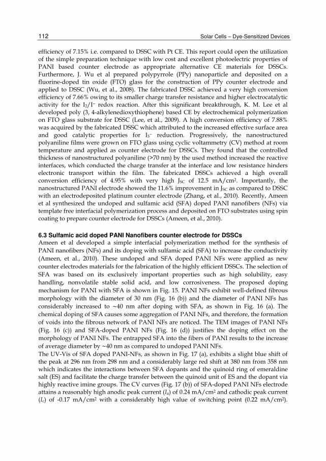
6.3 Sulfamic acid doped PANI Nanofibers counter electrode for DSSCs Ameen et al developed a simple interfacial polymerization method for the synthesis of
PANI nanofibers (NFs) and its doping with sulfamic acid (SFA) to increase the conductivity
(Ameen, et al., 2010). These undoped and SFA doped PANI NFs were applied as new
counter electrodes materials for the fabrication of the highly efficient DSSCs. The selection of
SFA was based on its exclusively important properties such as high solubility, easy
handling, nonvolatile stable solid acid, and low corrosiveness. The proposed doping
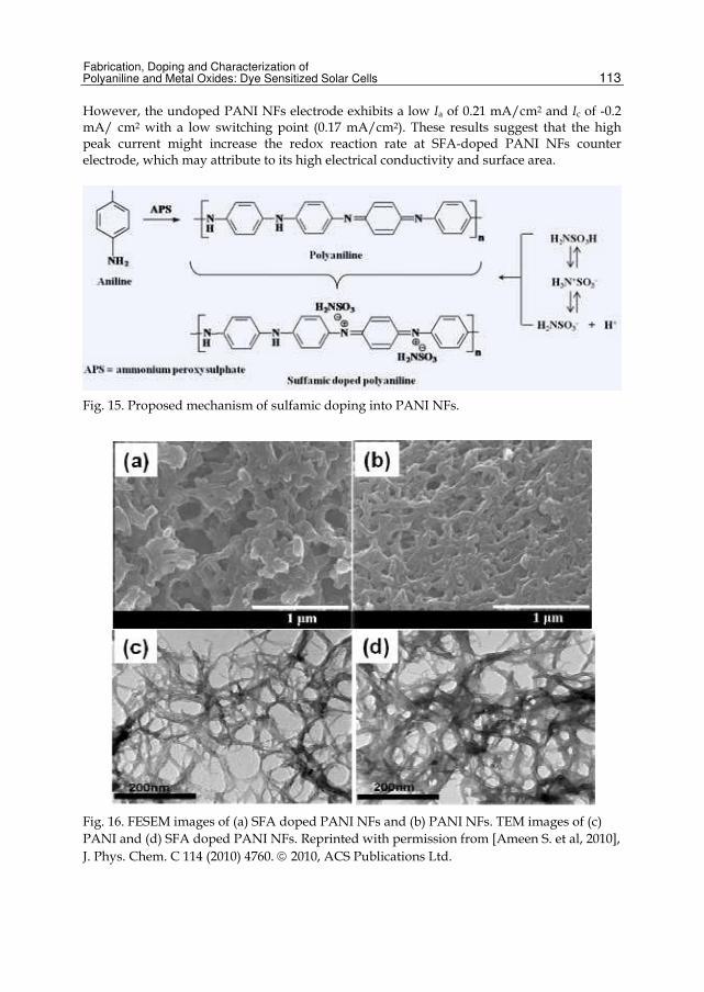
mechanism for PANI with SFA is shown in Fig. 15. PANI NFs exhibit well-defined fibrous
morphology with the diameter of 30 nm (Fig. 16 (b)) and the diameter of PANI NFs has
considerably increased to ∼40 nm after doping with SFA, as shown in Fig. 16 (a). The
chemical doping of SFA causes some aggregation of PANI NFs, and therefore, the formation
of voids into the fibrous network of PANI NFs are noticed. The TEM images of PANI NFs
(Fig. 16 (c)) and SFA-doped PANI NFs (Fig. 16 (d)) justifies the doping effect on the
morphology of PANI NFs. The entrapped SFA into the fibers of PANI results to the increase
of average diameter by ∼40 nm as compared to undoped PANI NFs.
The UV-Vis of SFA doped PANI-NFs, as shown in Fig. 17 (a), exhibits a slight blue shift of the peak at 296 nm from 298 nm and a considerably large red shift at 380 nm from 358 nm which indicates the interactions between SFA dopants and the quinoid ring of emeraldine salt (ES) and facilitate the charge transfer between the quinoid unit of ES and the dopant via highly reactive imine groups. The CV curves (Fig. 17 (b)) of SFA-doped PANI NFs electrode attains a reasonably high anodic peak current (Ia) of 0.24 mA/cm2 and cathodic peak current (Ic) of -0.17 mA/cm2 with a considerably high value of switching point (0.22 mA/cm2).
www.intechopen.com
Fabrication, Doping and Characterization of Polyaniline and Metal Oxides: Dye Sensitized Solar Cells
113
However, the undoped PANI NFs electrode exhibits a low Ia of 0.21 mA/cm2 and Ic of -0.2 mA/ cm2 with a low switching point (0.17 mA/cm2). These results suggest that the high peak current might increase the redox reaction rate at SFA-doped PANI NFs counter electrode, which may attribute to its high electrical conductivity and surface area.
Fig. 15. Proposed mechanism of sulfamic doping into PANI NFs.
Fig. 16. FESEM images of (a) SFA doped PANI NFs and (b) PANI NFs. TEM images of (c)
PANI and (d) SFA doped PANI NFs. Reprinted with permission from [Ameen S. et al, 2010],
J. Phys. Chem. C 114 (2010) 4760. 2010, ACS Publications Ltd.
www.intechopen.com

Solar Cells – Dye-Sensitized Devices
114
Fig. 17. (a) UV-vis spectra of PANI NFs and SFA-doped PANI NFs. (b) Cyclic voltammetry of iodide species on PANI NFs and SFA doped PANI NFs electrodes in acetonitrile solution with 10 mM LiI, 1 mM I2, and 0.1M LiClO4. Reprinted with permission from [Ameen S. et al, 2010], J. Phys. Chem. C 114 (2010) 4760. © 2010, ACS Publications Ltd.
Fig. 18. J-V curve of fabricated solar cell of PANI NFs and SFA doped PANI NFs as counter electrodes under light illumination of 100 mW/cm2. Reprinted with permission from
[Ameen S. et al, 2010], J. Phys. Chem. C 114 (2010) 4760. 2010, ACS Publications Ltd.
The Fig. 18 shows that the DSSCs fabricated with SFA-doped PANI NFs counter electrode achieve a high conversion efficiency (η) of 5.5% with a high short circuit current (JSC) of 13.6 mA/cm2, open circuit voltage (VOC) of 0.74 V, and fill factor (FF) of 0.53. The conversion efficiency increases by ∼27% and thus, after SFA doping of PANI NFs the conversion efficiency reaches the value of 5.5% than that of DSSC fabricated with PANI NFs counter electrode (4.0%). Further, the SFA-doped PANI NFs counter electrode has significantly increased the JSC and VOC of ∼20% and ∼10%, respectively, as compared to the DSSC fabricated with PANI NFs counter electrode. It indicates that the SFA doping has increased the fast reaction of I-/I3- species at counter electrode and therefore, the superior photovoltaic properties such as η, JSC, and VOC of the cell are attributed to the sufficiently high conductivity and electrocatalytic activity of doped PANI NFs, which alleviates the reduction of I3- at the thin SFA-doped PANI NFs layers. Importantly, the IPCE curves of DSSCs fabricated with PANI NFs counter electrode exhibit the low IPCE of ∼54% in the absorption range of 400-650 nm.
www.intechopen.com
Fabrication, Doping and Characterization of Polyaniline and Metal Oxides: Dye Sensitized Solar Cells
115
The IPCE value has prominently increased by ∼70% with the SFA doped PANI NFs counter electrode-based DSSCs. It is noteworthy that the IPCE of the device is considerably enhanced by ∼24% upon SFA doping on PANI NFs-based counter electrodes. The enhanced IPCE in DSSCs with SFA-doped PANI NFs electrode results in the high JSC and photovoltaic performance, which are related to its high electrical conductivity and the higher reduction of I3-
to I- in the electrolyte at the interface of PANI NFs layer and electrolyte.
7. Fabrication of DSSCs with metal oxide nanomaterials photoanodes
In DSSCs, the choice of semiconductor is governed by the conduction band energy and density of states which facilitate the charge separation and minimizing the recombination. Secondly, the high surface area and morphology of semiconductor are important to maximize the light absorption by the dye molecules while maintaining the good electrical connectivity with the substrate (Baxtera, et al., 2006).The semiconducting metal oxides such as TiO2, ZnO and SnO2 etc have shown good optical and electronic properties and are accepted as the effective photoelectrode materials for DSSCs. These metal oxide nanostructures present discrete morphologies of nanoparticles (Ito, et al., 2008) nanowires (Law, et al., 2005 & Feng, et al., 2008) and nanotubes (Macak, et al., 2005 & Mor et al., 2005) which are the key component in DSSCs for the effective dye adsorption and the efficient electron transfer during the working operation of DSSCs. To improve the light harvesting efficiency, the metal oxide nanostructures must possess high surface to volume ratio for high absorption of dye molecules. These metal oxide nanostructures are usually prepared by the methods like hydrothermal synthesis (Zhang, et al., 2003 & Wang et al., 2009) template method (Ren, et al., 2009 & Tan, et al., 2008) electrodeposition (Tsai, et al., 2009) and potentiostatic anodization (Chen, et al., 2009 & kang, et al., 2009) and are important for improving the photovoltaic properties of DSSCs such as JSC, VOC, FF and conversion efficiency. Out of these, TiO2 has been intensively investigated for their applications in photocatalysis and photovoltaic (Regan, et al., 1991 & Duffie, et al., 1991). Particularly in DSSCs, the porous nature of nanocrystalline TiO2 films provides the large surface for dye-molecule adsorption and therefore, the suitable energy levels at the semiconductor–dye interface (the position of the conduction-band of TiO2 being lower than the excited-state energy level of the dye) allow for the effective injection of electrons from the dye molecules to the semiconductor. Compared with other photovoltaic materials, anatase phase TiO2 is outstanding for its stability and wide band gap and thus, widely used in the devices (Gratzel, et al., 2001). On the other hand, ZnO nanomaterials are chosen as an alternative material to TiO2 photoanode due to its wide-band-gap with higher electronic mobility which would be favorable for the efficient electron transport, with reduced recombination loss in DSSCs. Studies have already been reported on the use of ZnO material photoanode for the application in DSSCs. Although the conversion efficiencies of ZnO (0.4–5.8%) is comparably lower than TiO2 (11%) but still ZnO is a distinguished alternative to TiO2 due to its ease of crystallization and anisotropic growth. In this part of the chapter, the various nanostructures of TiO2 and ZnO have been briefly summarized for the application for DSSCs.
7.1 Various TiO2 nanostructures photoanodes for DSSCs 7.1.1 Photoanodes with TiO2 nanotubes TiO2 nanotubes (NTs) arrays are generally synthesized by the methods like electrochemical approach (Zwilling, et al., 1999 & Gong, et al., 2001) layer-by-layer assembly (Guo, et al.,
www.intechopen.com
Solar Cells – Dye-Sensitized Devices
116
2005) template synthesis, sol–gel method (Martin, et al., 1994, Limmer, et al., 2002 & Lakshmi, et al., 1997) etc and are the effective photoanode for the fabrication of DSSCs. The reported methods for the synthesis of TiO2 NTs provide low yield and demand advanced technologies with the high cost of templates (anodic aluminum oxide, track-etched polycarbonate or the amphiphilic surfactants). A. J. Frank obtained the bundle-free and crack-free NT films by using the supercritical CO2 drying technique and found that the charge transport was considerably increased with the decreased of NTs bundles which created the additional pathways through the intertube contacts. However, J. H. Park et al. reported a simple and inexpensive methodology for preparing TiO2 NTs arrays on FTO glass and applied as photoanodes for DSSCs which exhibited the significantly high overall conversion efficiency of 7.6% with high JSC of 16.8 mA/cm2, VOC of 0.733 V and a fill factor (FF) of 0.63. The enhanced photovoltaic performance was attributed to the reduced charge recombination between photoinjected electrons in the substrate via tubular morphology of TiO2 photoanode (Park, et al., 2008).
7.1.2 Photoanodes with TiO2 nanorods The Highly crystalline TiO2 nanorods (NRs) with lengths of ~100-300 nm and diameters of ~20-30 nm were grown by J. Jui et al using the hydrothermal process with cetyltrimethylammonium bromide surfactant solution (Jiu, et al., 2006). In this synthesis, the length of nanorods was substantially controlled and maintained by the addition of a tri-block copolymer poly-(ethylene oxide) 100-poly (propylene oxide) 65-poly (ethylene oxide) 100 (F127) and polymer decomposed after sintering of TiO2 nanorods at high temperatures. The fabricated DSSCs attained a high overall conversion efficiency of 7.29% with considerably high VOC of 0.767 V and fill factor of 0.728. The enhancement in the photovoltaic properties was attributed to increase the ohmic loss and high electron transfer through TiO2 NRs. As compared to P-25 based DSSCs, the less amount of dye was absorbed by the TiO2 NRs photoanode might due to the larger size of the nanorods and therefore, result a slightly lower photocurrent density of 13.1 mA/cm2. B. Liu group proposed a hydrothermal process to develop the oriented single-crystalline TiO2 NRs or nanowires on a transparent conductive substrate (Liu, et al., 2009). The DSSCs fabricated with TiCl4 generated 4 μm-long rutile TiO2 NRs electrode and demonstrated relatively low light-to-electricity conversion efficiency of 3% with JSC ∼6.05 mA/cm2, VOC of ∼0.71 V, and FF of 0.7. The device delivered the improved IPCE of ∼50% at the peak of the dye absorption. The improved VOC and FF revealed that the TiCl4 treatment decreased the surface recombination. Conclusively, TiO2 NRs improved the dye adsorption and the optical density through the surface of oriented NRs.
7.1.3 Photoanodes with TiO2 nanowires Single-crystal-like anatase TiO2 nanowires (NWs) as compared to NRs and NTs morphology are extensively applied as photoanode for the fabrication of DSSCs. The perfectly aligned morphology of TiO2 NWs and networks of NWs could be achieved by the solution, electrophoretic and hydrothermal process due to the “oriented attachment” mechanism. The aligned TiO2 network with single-crystal anatase NWs conducted the high rate of electron transfer and achieved significantly high overall conversion efficiency of 9.3% with high JSC of 19.2 mA/cm2, VOC of 0.72 V, and FF of 0.675. The improved photovoltaic performance was ascribed to the network structure of single-crystal-like anatase NWs which acquired a high surface to volume ratio and thus, presented the high IPCE of ~ 90%. Recently, J. K. Oh
www.intechopen.com

Fabrication, Doping and Characterization of Polyaniline and Metal Oxides: Dye Sensitized Solar Cells
117
et al reported the branched TiO2 nanostructure photoelectrodes for DSSCs with TiO2 NWs as a seed material (Oh, et al., 2010). The prepared TiO2 electrode possessed a three-dimensional structure with rutile phase and showed high conversion efficiency of 4.3% with high JSC of 12.18 mA/cm2. Compared to DSSCs with TiO2 NWs, the cell performance and JSC was enhanced by 2 times, which was due to the increased specific surface area and the roughness factor. However, the lower FF was originated from the branches of TiO2 electrodes, resulting in the reduction of grain boundaries.
7.2 Various ZnO nanostructures photoanodes for DSSCs 7.2.1 Photoanodes with ZnO nanoparticles The techniques like vapor liquid solid, chemical vapor deposition, electron beam evaporation, hydro thermal deposition, electro chemical deposition and thermal evaporation etc are generally applied for the synthesis of ZnO nanostructures. Out of these, the chemical solution method is the simplest procedure for achieving uniform ZnO nanoparticles (NPs) thin films and delivers almost the same performance as that of nanocrystalline TiO2 with similar charge transfer mechanism between the dye and semiconductor. The synthesis of ZnO NPs is reported by the preparation of ZnO sols with zinc acetate as precursor and lithium hydroxide to form homogeneous ethanolic solutions (Spanhel, et al., 1991 & Keis, et al., 2001). Several researchers have fabricated DSSCs using sol–gel-derived ZnO NPs films and reported the low conversion efficiencies with values generally around 0.4–2.22% (Redmond, et al., 1994, Rani, et al., 2008 & Zeng, et al., 2006). Highly active ZnO nanoparticulate thin film through a compression method was prepared for high dye absorption by Keis et al for the fabrication of DSSCs (Keis, et al., 2002, 2002). The morphology of ZnO NPs, synthesized by a sol–gel route exhibited an average size of 150 nm. The thin film photoelectrodes were prepared by compressing the ZnO NPs powder under a very high pressure and the DSSCs fabricated with the obtained film achieved a very high overall conversion efficiency of 5% under the light intensity of 10 mWcm2.
7.2.2 Photoanodes with ZnO nanosheets and other nanostructures ZnO nanosheets (NSs) are quasi-two-dimensional structures that could be fabricated by a re-hydrothermal growth process of hydrothermally grown ZnO NPs (Suliman, et al., 2007). M. S. Akhtar et al prepared sheet-spheres morphology of ZnO nanomaterials through citric acid assisted hydrothermal process with 5 M NaOH solution (Akhtar, et al., 2007). The high conversion efficiency and high photocurrent of ZnO NSs based DSSCs was attributed to the effective high light harvesting by the maximum dye absorption via ZnO NSs film surface which promoted a better pathway for the charge injection into the ZnO conduction layer. Sequentially, C. F. Lin et al fabricated a prepared ZnO nanobelt arrays on the FTO substrates by an electrodeposition method and applied as photoelectrode for the fabrication of DSSCs (Lin, et al., 2008). Y. F. Hsu et al had grown a 3-D structure ZnO tetrapod nanostrcutures, comprised of four arms which were extended from a common core (Hsu, et al., 2008 & Chen, et al., 2009). The length of the arms was adjusted within the range of 1–20 mm, while the diameter was tuned from 100 nm to 2 μm by changing the substrate temperature and the oxygen partial pressure during vapor deposition.
7.2.3 Photoanodes with ZnO nanowires Law et al designed ZnO nanowire (NWs) arrays to increase the electron diffusion length and was applied as photoelectrode for the fabrication of DSSCs (Law, et al., 2005 & Greene, et al.,
www.intechopen.com

Solar Cells – Dye-Sensitized Devices
118
2006). The grown ZnO nanowires arrays films exhibited the relatively good resistivity values between the range of 0.3 to 2.0 Ω cm for the individual nanowires with an electron concentration of 1 - 5 x 1018 cm3 and a mobility of 1–5 cm2V-1s-1. The overall conversion efficiencies of 1.2-1.5% were obtained by DSSCs fabricated with ZnO nanowires arrays with short-circuit current densities of 5.3–5.85 mA/cm2, open-circuit voltages of 0.610–0.710 V, and fill factors of 0.36–0.38. Another group synthesized ZnO NWs by the use of ammonium hydroxide for changing the supersaturation degree of Zn precursors in solution process (Regan, et al., 1991). The length-to-diameter aspect ratio of the individual nanowires was easily controlled by changing the concentration of ammonium hydroxide. The fabricated DSSCs exhibited remarkably high conversion efficiency of 1.7% which was much higher than DSSC with ZnO nanorod arrays (Gao, et al., 2007). C. Y. Jiang et al reported the flexible DSSCs with a highly bendable ZnO NWs film on PET/ITO substrate which was prepared by a low-temperature hydrothermal growth at 85 °C (Jiang, et al., 2008). The fabricated composite films obtained by immersing the ZnO NPs powder in a methanolic solution of 2% titanium isopropoxide and 0.02 M acetic acid was treated with heat which favored the good attachment of NPs onto NWs surfaces (Jiang, et al., 2008). Here, the conversion efficiency of the fabricated DSSCs was achieved less as compared to DSSCs based on NPs.
7.2.4 Photoanodes with ZnO nanorods A. J. Cheng et al synthesized aligned ZnO nanorods (NRs) on indium tin oxide (ITO) coated glass substrate via a thermal chemical vapor deposition (CVD) (Cheng, et al., 2008) at very high temperature which affected the crystalline properties of ZnO NRs. The rapid large-scale synthesis of well-crystalline and good surface area of hexagonal-shaped ZnO NRs was carried out by A. Umar et al at very low temperature (70C) for the application of DSSCs (Umar, et al., 2009). A high overall light to electricity conversion efficiency of 1.86% with high fill factor (FF) of 74.4%, high open-circuit voltage (VOC) of 0.73V and short-circuit current (JSC) of 3.41mA/cm2 was achieved by fabricated DSSCs. M. S. Akhtar et al reported the morphology of ZnO flowers through hydrothermal process using Zinc acetate, NaOH and ammonia as capping agent. The photoanode was prepared by spreading the ZnO paste on FTO substrate by doctor blade technique for the fabrication of DSSCs (Akhatr, et al., 2007). Unfortunately, the DSSC presented a very low conversion efficiency of 0.3% with high FF of 0.54. The low performance might attribute to the low dye absorption on the surface of ZnO due to the less uniformity of the thin film with low surface to volume ratio. Furthermore, a flower like structures comprised with nanorods/nanowires can be assumed to deliver a larger surface area and a direct pathway for electron transport with the channels arisen from the branched to nanrods/nanowire backbone. Recently, hydrothermally grown ZnO nanoflower films accomplished improved overall conversion efficiency of 1.9% with high JSC of 5.5mA cm2, and a fill factor of 0.53 (Jiang, et al., 2007) which is higher than nanorod arrays films based DSSC of the conversion efficiency 1.0%, JSC 4.5 mA/cm2, and FF 0.36.
7.2.5 Photoanodes with ZnO nanotubes L. Vayssiers et al grown the ZnO microtubes arrays by thermal decomposition of a Zn2+
amino complex at 90°C in a regular laboratory oven (Vayssieres, et al., 2001). The
synthesized ZnO microtubes arrays possessed a high porosity and large surface area as
compared to ZnO NWs arrays. A. B. F. Martinson et al fabricated the ZnO nanotubes (NTs)
arrays by coating anodic aluminum oxide (AAO) membranes via atomic layer deposition
www.intechopen.com

Fabrication, Doping and Characterization of Polyaniline and Metal Oxides: Dye Sensitized Solar Cells
119
(ALD) and constructed the DSSCs which showed a relatively low conversion efficiency of
1.6% due to the less roughness factor of commercial membranes (Martinson, et al., 2007). In
continuity, Ameen et al reported the aligned ZnO NTs, grown at low temperature and
applied as photoanode for the performances of DSSCs (Ameen, et al., 2011). The ZnO seeded
FTO glass substrate supported the synthesis of highly densely aligned ZnO NTs whereas,
non-seeded FTO substrates generated non-aligned ZnO NTs. The non-aligned ZnO NTs
photoanode based fabricated DSSCs reported the low solar-to-electricity conversion
efficiency of ∼0.78%. However, DSSC fabricated with aligned ZnO NTs photoanode showed
three times improved solar-to-electricity conversion efficiency than DSSC fabricated with
non-aligned ZnO NTs. Fig. 19 shows the surface FESEM images of ZnO NTs deposited on
non-seeded and ZnO seeded FTO substrates. Fig. 19 (a & b) exhibits the highly densely
aligned ZnO NTs, substantially grown on ZnO seeded FTO substrates. Importantly, the
ZnO NTs possess a hexagonal hollow structure with average inner and outer diameter of ∼150nm and ∼300 nm, respectively, as shown in Fig. 19 (c & d). However, non-seeded FTO
substrates (Fig. 19 (e)) obtain the random and non-aligned morphology of NTs with the
average diameter of 800 nm. The high resolution image clearly displays the typical
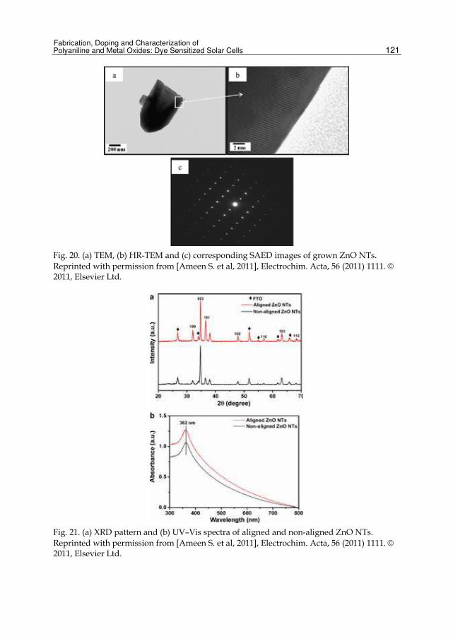
hexagonal hollow and round end of the NTs (Fig. 19 (f)). Fig. 20(a) of TEM image reveals
hollow NT morphology with the outer and inner diameter of ∼250nm and ∼100 nm,
respectively. SAED patterns (Fig. 20 (c)) exhibits a single crystal with a wurtzite hexagonal
phase which is preferentially grown in the [0001] direction. It is further confirmed from the
HRTEM image of the grown ZnO NTs, presented in Fig. 20(b). HRTEM image shows well-
resolved lattice fringes of crystalline ZnO NTs with the inter-planar spacing of ∼0.52nm.
Additionally, this value corresponds to the d-spacing of [0001] crystal planes of wurtzite
ZnO. Thus, the synthesized ZnO NTs is a single crystal and preferentially grown along the
c-axis [0001].
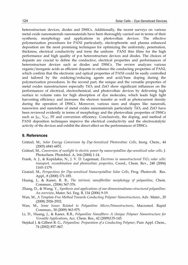
The XRD peaks (Fig 21 (a)) of grown aligned ZnO NTs on the seeded substrates appear at the same position but with high intensity might due to high crystalline properties of aligned morphology of ZnO NTs. The UV-Vis spectra as shown in Fig 21 (b)) exhibit a single peak which indicates that the grown ZnO NTs do not contain impurities. Moreover, the aligned morphology of ZnO NTs attains high absorption, indicating the higher crystalline properties than non-aligned ZnO NTs. The Raman spectra of non- aligned and aligned ZnO NTs is shown in Fig 22 (a). The grown
ZnO NTs exhibits a strong Raman peak at ∼437cm−1 corresponds to E2 mode of ZnO crystal
and two small peaks at ∼330cm−1 and ∼578cm−1 are assigned to the second order Raman
spectrum arising from zone-boundary phonons 3E2H–E2L for wurtzite hexagonal ZnO single
crystals and E1 (LO) mode of ZnO associated with oxygen deficiency in ZnO nanomaterials
respectively (Exarhas, et al., 1995). Compared to non-aligned ZnO NTs, the stronger E2
mode and much lower E1 (LO) mode indicates the presence of lower oxygen vacancy. The
Raman active E2 mode with high intensity and narrower spectral width is generally ascribed
to the better optical and crystalline properties of the materials (Serrano, et al., 2003) and
thus, the grown aligned ZnO NTs results high crystallinity of ZnO crystals with less oxygen
vacancies. Fig 22 (b) depicts the PL spectra of grown non-aligned and aligned ZnO NTs. An
intensive sharp UV emission at ∼378nm and a broader green emission at ∼581nm are
attributed to the free exciton emission from the wide band gap of ZnO NTs and the
recombination of electrons in single occupied oxygen vacancies in ZnO nanomaterials
(Vanheusden, et al., 1996). The high intensity and less broaden green emission indicates that
www.intechopen.com

Solar Cells – Dye-Sensitized Devices
120
the aligned ZnO NTs exhibits less oxygen vacancies and considerable stoichiometric phase
structure formation. Thus, the PL spectra suggest that ZnO seeding on FTO substrates might
improve surface-to-volume ratio and optical properties of ZnO NTs.
Fig. 19. FESEM images of aligned ZnO NTs (a) at low magnification and (b–d) at high magnification. (e) non-aligned ZnO NTs images at low magnification and (f) at high magnification. Reprinted with permission from [Ameen S. et al, 2011], Electrochim. Acta, 56
(2011) 1111. 2011, Elsevier Ltd.
www.intechopen.com
Fabrication, Doping and Characterization of Polyaniline and Metal Oxides: Dye Sensitized Solar Cells
121
Fig. 20. (a) TEM, (b) HR-TEM and (c) corresponding SAED images of grown ZnO NTs.
Reprinted with permission from [Ameen S. et al, 2011], Electrochim. Acta, 56 (2011) 1111. 2011, Elsevier Ltd.
Fig. 21. (a) XRD pattern and (b) UV–Vis spectra of aligned and non-aligned ZnO NTs.
Reprinted with permission from [Ameen S. et al, 2011], Electrochim. Acta, 56 (2011) 1111. 2011, Elsevier Ltd.
www.intechopen.com

Solar Cells – Dye-Sensitized Devices
122
Fig. 22. (a) Raman spectra and (b) photoluminescence spectra of aligned and nonaligned ZnO NTs. Reprinted with permission from [Ameen S. et al, 2011], Electrochim. Acta, 56
(2011) 1111. 2011, Elsevier Ltd.
Fig. 23. J–V curve of the DSSCs fabricated with aligned and non-aligned ZnO NTs photoanode. Reprinted with permission from [Ameen S. et al, 2011], Electrochim. Acta, 56 (2011) 1111. © 2011, Elsevier Ltd.
www.intechopen.com

Fabrication, Doping and Characterization of Polyaniline and Metal Oxides: Dye Sensitized Solar Cells
123
Fig. 24. IPCE curves of the DSSCs fabricated with aligned and non-aligned ZnO NTs photoanode. Reprinted with permission from [Ameen S. et al, 2011], Electrochim. Acta, 56 (2011) 1111. © 2011, Elsevier Ltd.
Fig 23 shows that DSSCs fabricated with aligned ZnO NTs photoanode achieve high solar-to-electricity conversion efficiency of 2.2% with a high short circuit current (JSC) of 5.5 mA/cm2, open circuit voltage (VOC) of 0.65 V, and fill factor (FF) of 0.61. Compared with non-aligned ZnO NTs photoanode based DSSC, the aligned ZnO NTs photoanode has appreciably enhanced the conversion efficiency by three times with significantly improved JSC, VOC and FF. The DSSC fabricated with non-aligned ZnO NTs pho-to anode executes relatively low of 0.78 % with JSC of 2.2mA/cm2, VOC (0.60 V) and FF of 0.57. The enhanced photovoltaic performances and the improved JSC are mainly related to the highly dense morphology of aligned ZnO NTs and also, high dye absorption which leads to improved light harvesting efficiency. The aligned morphology might result from the sufficiently high surface area of ZnO NTs and thus, execute reasonably high charge collection and the transfer of electrons at the interface of ZnO NTs and electrolyte layer. While, low efficiency of non-aligned ZnO NTs might associate to low surface area of ZnO NTs and non-uniform surface which might result to low light harvesting efficiency and increases the recombination rate between the electrolyte and the FTO substrate. Ameen et al has reported that the performance of DSSCs with grown aligned ZnO NTs photoanode is significantly higher than the reported DSSCs with aligned ZnO nanorods, nanowires and nanotubes based photoanode (Pasquier, et al., 2006 & Singh, et al., 2010). Importantly, the aligned ZnO NTs based DSSC achieves a maximum IPCE value of ∼31.5% at ∼520nm as shown in Fig 24. The considerably low IPCE (∼21%) is obtained with non-aligned ZnO NTs photoanode based DSSC and thus, the aligned ZnO NTs photoanode presents approximately two times improved IPCE compared to non-aligned ZnO NTs photoanode. The enhancement in IPCE imputes the influence of highly ordered aligned ZnO NTs morphology with high surface area which might improve the light scattering capacities and provides the better interaction between the photons and the dye molecules (Tachibana, et al., 2002).
8. Conclusions
The chapter summarizes the synthesis of PANI through simple and novel polymerization techniques, the concept of doping, types of dopants and the application of PANI in
www.intechopen.com
Solar Cells – Dye-Sensitized Devices
124
heterostructure devices, diodes and DSSCs. Additionally, the recent surveys on various metal oxide nanomaterials nanomaterials have been thoroughly carried out in terms of their synthesis, morphology and applications in photovoltaic devices. The effective polymerization procedures for PANI particularly, electrophoretic and plasma enhanced deposition are the most promising techniques for optimizing the uniformity, penetration, thickness, electrical conductivity and form the uniform PANI thin films for the high performance and high quality of p-n heterostructure devices and diodes. The choices of dopants are crucial to define the conductive, electrical properties and performances of heterostructure devices such as diodes and DSSCs. The review analyzes various organic/inorganic acids as efficient dopants to enhance the conducting properties of PANI, which confirm that the electronic and optical properties of PANI could be easily controlled and tailored by the oxidizing/reducing agents and acid/base doping during the polymerization procedures. In the second part, the unique and the versatile properties of metal oxides nanostructures especially TiO2 and ZnO show significant influences on the performances of electrical, electrochemical, and photovoltaic devices by delivering high surface to volume ratio for high absorption of dye molecules, which leads high light harvesting efficiency and increases the electron transfer as well as photocurrent density during the operation of DSSCs. Moreover, various sizes and shapes like nanorods, nanowires and nanotubes of metal oxides nanomaterials particularly TiO2 and ZnO have been reviewed evidently in terms of morphology and the photovoltaic properties of DSSCs such as JSC, VOC, FF and conversion efficiency. Conclusively, the doping, and method of PANI deposition techniques improve the electrical conductivity and the electrocatalytic activity of the devices and exhibit the direct effect on the performances of DSSCs.
9. References
Grätzel, M., Solar Energy Conversion by Dye-Sensitized Photovoltaic Cells, Inorg. Chem., 44 (2005) 6841-6851.
Grätzel, M., Conversion of sunlight to electric power by nanocrystalline dye-sensitized solar cells, J. Photochem. Photobiol. A, 164 (2004) 1-14.
Frank, A. J., & Kopidakis, N., J. V. D. Lagemaat, Electrons in nanostructured TiO2 solar cells: transport, recombination and photovoltaic properties, Coord., Chem. Rev., 248 (2004) 1165–1179.
Gratzel, M., Perspectives for Dye-sensitized Nanocrystalline Solar Cells, Prog. Photovolt. Res. Appl., 8 (2000) 171-185.
Huang, J., & Kaner, R. B., The intrinsic nanofibrillar morphology of polyaniline, Chem. Commun., (2006) 367-376.
Zhang, D., & Wang, Y., Synthesis and applications of one-dimensionalnano-structured polyaniline: An overview, Mater. Sci. Eng. B, 134 (2006) 9-19.
Wan, M., A Template-Free Method Towards Conducting Polymer Nanostructures, Adv. Mater., 20 (2008) 2926-2932.
Wan, M., Some Issues Related to Polyaniline Micro-/Nanostructures, Macromol. Rapid Commun., 30 (2009) 963-975.
Li, D., Huang, J., & Kaner, R.B., Polyaniline Nanofibers: A Unique Polymer Nanostructure for Versatile Applications, Acc. Chem. Res., 42 (2009)135-145.
Stejskal J. & Gilbert R. G., Polyaniline. Preparation of a Conducting Polymer, Pure Appl. Chem., 74 (2002) 857–867.
www.intechopen.com

Fabrication, Doping and Characterization of Polyaniline and Metal Oxides: Dye Sensitized Solar Cells
125
Friend, R. H., Gymer, R.W., & Holmes, A. B., Electroluminescence in conjugated polymers, Nature (London), 397 (1999) 121-128.
Park J. K. & Kwon O-P., Enhanced electrical conductivity of polyaniline film by a low magnetic field, Synth. Met. 160 (2010) 728-731.
Gerard, M., Chaubey, A., & Malhotra, B. D., Application of conducting polymers to biosensors, Biosensor Bioeleton., 17 (2002) 345-359.
Xia, L., Wei, Z., & Wan, M., Conducting polymer nanostructures and their application in biosensors, J. Coll. Interf. Sci., 341 (2010) 1-11.
Smith, J. D. S., Intrinsically Electrically Conducting Polymers. Synthesis, Characterization and their Applications, Prog. Polym. Sci., 23 (1998) 57-79.
Wessling, B., From conductive polymers to organic metals, Chem. Innov., 31 (2001) 34-40. Cho, Y. H., Cho, M.S., Choi, H. J., & Jhon, M. S., Electrorheological characterization of
polyaniline-coated poly(methyl methacrylate)suspensions, Colloid Polym. Sci., 280 (2002) 1062-1066.
Choi, H. J., Cho, M. S., Kim, J.W., Kim, C.A., & Jhon, M. S., A yield stress scaling function for electrorheological fluids, Appl. Phys. Lett., 78 (2001) 3806-3809.
Ameen, S., Akhtar, M. S., & Husain, M., Polyaniline and Its Nanocomposites: Synthesis, Processing, Electrical Properties and Applications, Sci. Adv. Mater., 2 (2010) 441-462.
Huang, J. X., Virji, S., Weiller, B. H., & Kaner, R.B., Polyaniline Nanofibers: Facile Synthesis and Chemical Sensors, J. Am. Chem. Soc., 125 (2003) 314-315.
Virji, S., Huang, J. X., Kaner, R. B., & Weiller, B. H., Polyaniline Nanofiber Gas Sensors: Examination of Response Mechanisms, Nano Lett., 4 (2004) 491-496.
King, R. C. Y., & Rousse, l. F., Morphological and electrical characteristics of polyaniline nanifibers, Synth. Met., 153 (2005) 337-340.
Huang, J. X., & Kaner, R. B., A General Chemical Route to Polyaniline Nanofibers, J. Am. Chem. Soc., 126 (2004) 851-855.
Jing, X. L., Wang, Y.Y., Wu, D., She, L., & Guo, Y., Polyaniline Nanofibers Prepared with Ultrasonic Irradiation, J. Polym. Sci., Part A: Polym. Chem., 44 (2006) 1014-1019.
Jing, X. L., Wang, Y. Y., Wu, D., & Qiang, J.P., Sonochemical synthesis of polyaniline nanofibers, Ultrason. Sonochem. 14 (2007) 75-80.
Dhaoui, W., Zarrouk, H., & Pron, A., Spectroscopic properties of thin layers of sulfamic acid-doped polyaniline and their application to reagentless determination of nitrite, Synth. Metals, 157 (2007) 564-569.
Dhaoui, W., Bouzitoun, M., Zarrouk, H., Ouada, H. B., & Pron, A., Electrochemical sensor for nitrite determination based on thin films of sulfamic acid doped polyaniline deposited on Si/SiO2 structures in electrolyte/insulator/semiconductor (E.I.S.) configuration, Synth. Metals, 158 (2008) 722-726.
Ameen, S., Ali, V., Zulfequar, M., Haq, M. M., & Husain, M., Electrical conductivity and dielectric properties of sulfamic acid doped polyaniline, Curr. Appl. Phys., 7 (2007) 215-219.
Ameen, S., Akhtar, M. S., Kim, Y. S., Yang, O. B., & Shin, H. S., Sulfamic Acid-Doped Polyaniline Nanofibers Thin Film-Based Counter Electrode: Application in Dye-Sensitized Solar Cells, J. Phys. Chem. C, 114 (2010) 4760-4764.
Ameen, S., Ali, V., Zulfequar, M., Haq, M. M., & Husain, M., Preparation and measurements of electrical and spectroscopic properties of sodium thiosulphate doped polyaniline, Curr. Appl. Phys., 9 (2009) 478-483.

Solar Cells – Dye-Sensitized Devices
126
Ameen, S., Ali, V., Zulfequar, M., Haq, M. M., & Husain, M., Photoluminescence, FTIR, and Electrical Characterization of Samarium (III) Chloride-Doped Polyaniline, J. Appl. Polym. Sci., 112 (2009) 2315-2319.
Ameen, S., Ali, V., Zulfequar, M., Haq, M. M., & Husain, M., Preparation and measurements of electrical and spectroscopic properties of praseodymium (III) chloride-doped polyaniline, Physica E, 40 (2008) 2805-2809.
Ameen, S., Ali, V., Zulfequar, M. Haq, M. M., & Husain, M., DC Conductivity and Spectroscopic Characterization of Binary Dopant (ZrO2/AgI)-Doped Polyaniline, J. Polym. Sci.: Part B: Polym. Phys., 45 (2007) 2682-2687.
Wang, S., Tan, Z., Li, Y., Sun, L., & Zhang, T., Synthesis, characterization and thermal analysis of polyaniline/ZrO2 composites, Thermochim. Acta, 441 (2006) 191–194.
Ameen, S., Lakshmi, G. B. V. S., & Husain, M., Synthesis and characterization of polyaniline prepared with the dopant mixture of (ZrO2/PbI2), J. Phys. D: Appl. Phys. 42 (2009) 105104-105109.
Ameen, S., Akhtar, M. S., Ansari, S. G., Yang, O. B., & Shin, H. S., Electrophoretically deposited polyaniline/ZnO nanoparticles for p-n heterostructure diodes, Superlatt. Microstr., 46 (2009) 872-880.
Ameen, S., Akhtar, M. S., Kim, Y.S., Yang, O. B., & Shin, H. S., Diode Behavior of Electrophoretically Deposited Polyaniline on TiO2 Nanoparticulate Thin Film Electrode, J. Nanosci. Nanotech., 11(2011) 1559-1564.
Somani, P. R., Marimuthu, R., Mulik, U. P., Sainkar, S. R., & Amalnerkar, D. P., High piezoresistivity and its origin in conducting polyanilinerTiO2 Composites, Synth. Met., 106 (1999) 45-52.
Niu, Z., Yang, Z., Hu, Z., Lu, Y., & Han, C. C., Polyaniline-Silica Composite Conductive Capsules and Hollow Spheres, Adv. Funct. Mater., 13 (2003) 949-954.
Ameen, S., Ansari, S. G., Song, M., Kim, Y. S., & Shin, H. S., Fabrication of polyaniline/TiO2 heterojunction structure using plasma enhanced polymerization technique, Superlatt. Microstruc. 46 (2009) 745-751.
Ameen, S., Akhtar, M. S., Kim, Y. S., Yang, O. B., & Shin, H. S., Electrical and Structural Characterization of Plasma Polymerized Polyaniline/TiO2 Heterostructure Diode: A Comparative Study of Single and Bilayer TiO2 Thin Film Electrode, J. Nanosci. Nanotech. 11 (2011) 3306–3313.
Dhawale, D. S., Alunkhe, R. R. S., Patil, U. M., Gurav, K. V., More, A. M., & Lokhande, C. D., Room temperature liquefied petroleum gas (LPG) sensor based on p-polyaniline/n-TiO2 heterojunction, Sens. Actua. B, 134 (2008) 988–992.
Nadarajah, A., Word, R. C., Meiss, J.,& Konenkamp, R., Flexible Inorganic Nanowire Light-Emitting Diode, Nano Lett., 8 (2008) 534-537.
Maeng, J., Jo, M., Kang, S. J., Kwon, M. K., Jo, G., Kim, T. W., Seo, J., Hwang, H., Kim D. Y.,& Park S. J., T. Lee. Transient reverse current phenomenon in a p-n heterojunction comprised of poly (3,4-ethylene-dioxythiophene):poly(styrene-sulfonate) and ZnO nanowall, Appl. Phys. Lett., 93 (2008) 123109-123111.
Thompson, B. C., & Frechet, J. M. J., Polymer–Fullerene Composite Solar Cells, Angew. Chem.-Int. Ed., 47(2008) 58-77.
Gunes, S., Neugebauer, H., & Sariciftci, N. S., Conjugated Polymer-Based Organic Solar Cells, Chem. Rev., 107(2007)1324-1338.
Bundgaard, E., & Krebs, F. C., Low band gap polymers for organic photovoltaics, Sol. Energy Mater. Sol. Cells, 91(2007) 954-985.
Fabrication, Doping and Characterization of Polyaniline and Metal Oxides: Dye Sensitized Solar Cells
127
Shaw, P. E., Ruseckas, A., & Samuel, I. D. W., Exciton Diffusion Measurements in Poly(3-hexylthiophene), Adv. Mater., 20 (2008) 3516-3520.
Sirringhaus, H., Brown, P. J., Friend, R. H., Nielsen, M. M., Bechgaard, K., Langeveld V. B. M. W., Spiering, A. J. H., Janssen, R. A. J., Meijer, E. W., Herwig, P., & Leeuw, D. M. D., Two-dimensional charge transport in self-organized, high-mobility conjugated polymers, Nature, 401(1999) 685-688.
Waldauf, C., Morana, M., Denk, P., Schilinsky, P., Coakley, K., Choulis, S. A., & Brabec, C. J., Highly efficient inverted organic photovoltaics using solution based titanium oxide as electron selective contact, Appl. Phys. Lett., 89 (2006) 233517-233519.
Steim, R., Kogler, F. R., & Brabec, C. J., Interface materials for organic solar cells, J. Mater. Chem., 20 (2010) 2499-2512.
Steim, R., Choulis, S. A., Schilinsky, P., & Brabec, C. J., Interface modification for highly efficient organic photovoltaics, Appl. Phys. Lett., 92 (2008) 093303-093305.
Ameri, T., Dennler, G., Lungenschmied, C., & Brabec, C. J., Organic tandem solar cells: A review, Ener. Environ. Sci., 2 (2009) 347-363.
Lee Y. J., Ruby, D. S., Peters, D.W., McKenzie, B. B., & Hsu, J. W. P., ZnO Nanostructures as Efficient Antireflection Layers in Solar Cells, Nano Lett., 8 (2008) 1501-1505.
Cantu, M. L., IddikiM, K. S, Rojas, D. M., Amade, R., & Pech, N. I. G., Nb-TiO2/polymer hybrid solar cells with photovoltaic response under inert atmosphere conditions, Sol. Energy Mater. Sol. Cells, 94 (2010)1227-1234.
Cantu, M. L., Norrman, K., Andreasen, J.W., & Krebs, F.C., Oxygen Release and Exchange in Niobium Oxide MEHPPV Hybrid Solar Cells, Chem. Mater., 18 (2006) 5684-5690.
Cantu, M. L., Norrman, K., Andreasen, J.W., Pastor, N. C., & Krebs, F.C., Detrimental Effect of Inert Atmospheres on Hybrid Solar Cells Based on Semiconductor Oxides, J. Electrochem. Soc., 154 (2007) B508.
Cantu, M. L., & Krebs, F.C., Hybrid solar cells based on MEH-PPV and thin film semiconductor oxides (TiO2, Nb2O5, ZnO, CeO2 and CeO2–TiO2): Performance improvement during long-time irradiation, Sol. Energy Mater. Sol. Cells, 90 (2006) 2076-2086.
Valls, I. G., & Cantu, M. L., Dye sensitized solar cells based on vertically-aligned ZnO nanorods: effect of UV light on power conversion efficiency and lifetime, Ener. Environ. Sci., 3 (2010) 789-795.
Valls, I. G., & Cantu, M. L., Vertically-aligned nanostructures of ZnO for excitonic solar cells: a review, Ener. Environ. Sci., 2 (2009) 19-25.
Arici, E., Meissner, D., Schaffler, F., & Sariciftci, N.S., Core/shell nanomaterials in photovoltaics, Int. J. Photoenergy, 5 (2003) 199-208.
Sariciftci, N.S., Smilowitz, L., Heeger, A. J., & Wudl, F., Photoinduced Electron Transfer from a Conducting Polymer to Buckminsterfullerene, Science, 258 (1992) 1474-1476.
Yu, G., Gao, J., Hummelen, J.C., Wudl, F., & Heeger, A.J., Polymer Photovoltaic Cells: Enhanced Efficiencies via a Network of Internal Donor-Acceptor Heterojunctions, Science, 270 (1995) 1789-1791.
Ameen, S., Akhtar, M. S., Kim, G.S., Kim, Y. S., Yang, O. B., & Shin, H. S., Plasma-enhanced polymerized aniline/TiO2 dye-sensitized solar cells, J. Alloys Compd., 487 (2009) 382-386.
Saito, Y., Kitamura, T., Wada, Y., & Yanagida, S., Application of Poly (3,4-ethylenedioxythiophene) to Counter Electrode in Dye-Sensitized Solar Cells, Chem. Lett. 31 (2002) 1060-1063., Y. Saito, W. Kubo, T. Kitamura, Y. Wada, S. Yanagida, I−/I3− redox reaction behavior on poly(3,4-ethylenedioxythiophene) counter electrode in dye-sensitized solar cells, J. Photochem. Photobiol. A. Chem. 164 (2004) 153-157.
Solar Cells – Dye-Sensitized Devices
128
Li, Q., Wu, J., Tang, Q., Lan, Z., Li, P., Lin, J., & Fan, L., Application of microporous polyaniline counter electrode for dye-sensitized solar cells, Electrochem. Commun. 10 (2008) 1299-1302.
Wu, J., Li, Q., Fan, L., Lan, Z., Li, P., Lin, J., & Hao, S., High-performance polypyrrole nanoparticles counter electrode for dye-sensitized solar cells, J. Power Sour. 181 (2008) 172-176.
Lee, K. M., Chen, P. Y., Hsu, C. Y., Huang, J. H., Ho, W. H., Chen, H. C., & Ho, K. C., A high-performance counter electrode based on poly(3,4-alkylenedioxythiophene) for dye-sensitized solar cells, J. Power Sour. 188 (2009) 313-318.
Zhang, J., Hreid, T., Li, X., Guo, W., Wang, L., Shi, X., Su, H., & Yuan, Z., Nanostructured polyaniline counter electrode for dye-sensitised solar cells: Fabrication and investigation of its electrochemical formation mechanism, Electrochim. Acta, 55 (2010) 3664–3668.
Baxtera, J. B., & Aydil, E. S., Dye-sensitized solar cells based on semiconductor morphologies with ZnO nanowires, Sol. Energy Mater. Sol. Cells, 90 (2006) 607-622.
Ito, S., Murakami, T. N., Comte, P., Liska, P., Grätzel, C., & Nazeeruddin, M. K., Fabrication of thin film dye sensitized solar cells with solar to electric power conversion efficiency over 10%, Thin Solid Films, 14 (2008) 4613-4619.
Law, M., Greene, L. E., Johnson, J.C., Saykally, R., & Yang, P.D., Nanowire dye-sensitized solar cells, Nat. Mater., 6 (2005) 455-459.
Feng, X. J, Shankar, K., Varghese, O. K., Paulose, M., Latempa, T. J., & Grimes, C. A., Vertically Aligned Single Crystal TiO2 Nanowire Arrays Grown Directly on Transparent Conducting Oxide Coated Glass: Synthesis Details and Applications, Nano Lett., 11(2008)3781-3786.
Macak, J. M., Tsuchiya, H., & Schmuki, P., High-Aspect-Ratio TiO2 Nanotubes by Anodization of Titanium, Angew. Chem. Int Ed, 14 (2005) 2100-2102.
Mor, G. K., Shankar, K., Paulose, M., Varghese, O. K., & Grimes, C. A., Enhanced Photocleavage of Water Using Titania Nanotube Arrays, Nano Lett., 1 (2005) 191-195.
Zhang, D. S., Yoshida, T., & Minoura, H., Low-Temperature Fabrication of Efficient Porous Titania Photoelectrodes by Hydrothermal Crystallization at the Solid/Gas Interface, Adv Mater., 10 (2003) 814-817.
Wang, H., Liu, Y., Li, M., Huang, H., Zhong, M.Y., & Shen, H., Hydrothermal growth of large-scale macroporous TiO2 nanowires and its application in 3D dye-sensitized solar cells, Appl. Phys. A, 97 (2009) 25-29.
Ren, X., Gershon, T., Iza, D. C, Rojas, D. M., Musselman, K., & Driscoll, J. L. M., The selective fabrication of large-area highly ordered TiO2 nanorod and nanotube arrays on conductive transparent substrates via sol–gel electrophoresis, Nanotechnology, 36 (2009) 365604-9.
Tan, L. K., Chong, M. A. S., & Gao, H., Free-Standing Porous Anodic Alumina Templates for Atomic Layer Deposition of Highly Ordered TiO2 Nanotube Arrays on Various Substrates, J. Phys. Chem. C, 112 (2008) 69-73.
Tsai, T.Y., & Lu, S.Y., A novel way of improving light harvesting in dye-sensitized solar cells – Electrodeposition of titania, Electrochem. Commun., 11 (2009) 2180-2183.
Chen, Q.W., & Xu, D.S., Large-Scale, Noncurling, and Free-Standing Crystallized TiO2 Nanotube Arrays for Dye-Sensitized Solar Cells, J. Phys. Chem. C, 113 (2009) 6310-6314.
Kang, T. S., Smith, A. P., Taylor, B. E., & Durstock, M. F., Fabrication of highly-ordered TiO2 nanotube arrays and their use in dye-sensitized solar cells, Nano. Lett., 9 (2009) 601-606.
Regan, B. O., & Graetzel, M., A low-cost, high-efficiency solar cell based on dye-sensitized colloidal TiO2 films, Nature, 353 (1991) 737-740.
Duffie, J., & Beckman, W., Solar Engineering of Thermal Processes. Wiley: U.S.A., 1991

Fabrication, Doping and Characterization of Polyaniline and Metal Oxides: Dye Sensitized Solar Cells
129
Graetzel, M., Photoelectrochemical cells, Nature, 414 (2001) 338-344. Zwilling, V., Aucouturier, M., & Ceretti, E. D., Anodic oxidation of titanium and TA6V alloy in
chromic media. An electrochemical approach, Electrochem. Acta, 45 (1999) 921-929. Gong, D., Grimes, C. A., Varghese, O. K., Hu, W., Singh, R. S., Chen, Z., & Dickey E.C.,
Titanium oxide nanotube arrays prepared by anodic oxidation, J. Mater. Res., 16 (2001) 3331-3334.
Guo, Y. G., Hu, J. S., Liang, H. P., Wan, L. J., & Bai, C.L., TiO2-Based Composite Nanotube Arrays Prepared via Layer-by-Layer Assembly, Adv. Funct. Mater., 15 (2005) 196.
Martin, C. R., Nanomaterials: A Membrane-Based Synthetic Approach, Science, 266 (1994) 1961-1966.
Limmer, S. J., Seraji, S., Wu, Y., Chou, T. P., Nguyen, C., & Cao, G. Z., Template-Based Growth of Various Oxide Nanorods by Sol–Gel Electrophoresis, Adv. Funct. Mater., 12 (2002) 59-64.
Lakshmi, B. B., Dorhout, P. K., & Martin, C. R., Sol−Gel Template Synthesis of Semiconductor Nanostructures, Chem. Mater., 9 (1997) 857-862.
Park, J. H., Lee, T.W., & Kang, M.G., Growth, detachment and transfer of highly-ordered TiO2 nanotube arrays: use in dye-sensitized solar cells, Chem. Commun., (2008) 2867-2869.
Jiu, J., Isoda, S., Wang, F., & Adachi, M., Dye-Sensitized Solar Cells Based on a Single-Crystalline TiO2 Nanorod Film, J. Phys. Chem. B, 110 (2006) 2087-2092.
Liu, B., & Aydil, E. S., Growth of Oriented Single-Crystalline Rutile TiO2 Nanorods on Transparent Conducting Substrates for Dye-Sensitized Solar Cells, J. Am. Chem. Soc., 131(2009) 3985-3990.
Oh, J. K., Lee, J. K., Kim, H.S., Han, S. B., & Park, K.W., TiO2 Branched Nanostructure Electrodes Synthesized by Seeding Method for Dye-Sensitized Solar Cells, Chem. Mater., 22 (2010) 1114-1118.
Spanhel, L., & Anderson, M. A., Semiconductor clusters in the sol-gel process: quantized aggregation, gelation, and crystal growth in concentrated zinc oxide colloids, J. Am. Chem. Soc., 113(1991) 2826-2833.
Keis, K., Vayssieres, L., Rensmo, H., Lindquist, S. E., & Hagfeldt, A., Photoelectrochemical properties of nano-to microstructured ZnO electrodes, J. Electrochem. Soc., 148 (2001) A149-153.
Redmond, G., Fitzmaurice, D., & Graetzel, M., Visible Light Sensitization by cis-Bis(thiocyanato)bis(2,2'-bipyridyl-4,4'-dicarboxylato)ruthenium (II) of a Transparent Nanocrystalline ZnO Film Prepared by Sol-Gel Techniques, Chem. Mater., 6(1994) 686-691.
Rani, S., Suri, P., Shishodia, P. K., & Mehra, R. M., Synthesis of nanocrystalline ZnO powder via sol–gel route for dye-sensitized solar cells, Sol. Energ. Mat. Sol. C, 92 (2008) 1639-1645.
Zeng, L. Y., Dai, S. Y., Xu, W. W., & Wang, K. J., Dye-Sensitized Solar Cells Based on ZnO Films, Plasma Sci. Tech., 8 (2006) 172-176.
Keis, K., Bauer, C., Boschloo, G., Hagfeldt, A., Westermark, K., Rensmo, H., & Siegbahn, H., Nanostructured ZnO electrodes for dye-sensitized solar cell applications, J. Photochem. Photobiol. A: Chem., 148(2002) 57-64.
Keis, K., Magnusson, E., Lindstrom, H., Lindquist, S. E., & Hagfeldt, A., A 5% efficient photoelectrochemical solar cell based on nanostructured ZnO electrodes, Sol. Energ. Mat. Sol. Cells, 73(2002) 51-58.
Suliman, A. E., Tang, Y. W., & Xu, L., Preparation of ZnO nanoparticles and nanosheets and their application to dye-sensitized solar cells, Sol. Energ. Mat. Sol. Cells, 91(2007) 1658-1662.

Solar Cells – Dye-Sensitized Devices
130
Akhtar, M. S., Khan, M. A., Jeon, M. S., & Yang, O. B., Controlled synthesis of various ZnO nanostructured materials by capping agents-assisted hydrothermal method for dye-sensitized solar cells, Electrochim. Acta, 53(2008) 7869-7874.
Lin, C. F., Lin, H., Li, J. B., & Li, X., Electrodeposition preparation of ZnO nanobelt array films and application to dye-sensitized solar cells, J. Alloys Compd., 462 (2008)175-180
Hsu, Y. F., Xi, Y. Y., Yip, C. T., Djurisic, A. B., & Chan, W. K., Dye-sensitized solar cells using ZnO tetrapods, J. Appl. Phys., 103(2008) 083114-083117.
Chen, W., Zhang, H. F., Hsing, I. M., & Yang, S. H., A new photoanode architecture of dye sensitized solar cell based on ZnO nanotetrapods with no need for calcination, Electrochem. Commun., 11(2009) 1057-1060.
Law, M., Greene, L. E., Johnson, J. C., Saykally, R., & Yang, P. D., Nanowire dye-sensitized solar cells, Nat. Mater., 4 (2005) 455-459.
Greene, L. E., Yuhas, B. D., Law, M., Zitoun, D., & Yang, P. D., Solution-Grown Zinc Oxide Nanowires, Inorg. Chem., 45(2006) 7535-7543.
Gao, Y. F., Nagai, M., Chang, T. C., & Shyue, J. J., Solution-Derived ZnO Nanowire Array Film as Photoelectrode in Dye-Sensitized Solar Cells, Cryst. Grow. Des. 7 (2007) 2467-2471.
Jiang, C. Y., Sun, X. W., Tan, K. W., Lo, G. Q., Kyaw, A. K. K., & Kwong, D. L., High-bendability flexible dye-sensitized solar cell with a nanoparticle-modified ZnO-nanowire electrode, Appl. Phy. Lett., 92(2008) 143101-143103.
Cheng, A. J., Tzeng, Y., Zhou, Y., Park, M., Wu, T.H., Shannon, C., Wang, D., & Lee, W., Thermal chemical vapor deposition growth of zinc oxide nanostructures for dye-sensitized solar cell fabrication, Appl. Phys. Lett., 92 (2008) 092113-092115
Umar, A., Al-Hajry, A., Hahn, Y.B., & Kim, D.H., Rapid synthesis and dye-sensitized solar cell applications of hexagonal-shaped ZnO nanorods, Electrochim. Acta, 54 (2009) 5358-5362.
Jiang, C. Y., Sun, X. W., Lo, G. Q., Kwong, D. L., & Wang, J. X., Improved dye-sensitized solar cells with a ZnO-nanoflower photoanode, Appl. Phy. Lett. 2007, 90, 263501-263503.
Vayssieres, L., Keis, K., Hagfeldt, A., & Lindquist, S. E., Three-Dimensional Array of Highly Oriented Crystalline ZnO Microtubes, Chem. Mater., 13(2001) 4395-4398.
Martinson, A. B. F., Elam, J. W., Hupp, J. T., & Pellin, M. J., ZnO Nanotube Based Dye-Sensitized Solar Cells, Nano Lett., 7(2007) 2183-2187.
Ameen, S., Akhtar, M. S., Kim, Y.S., Yang, O. B., & Shin, H. S., Influence of seed layer treatment on low temperature grown ZnO nanotubes: Performances in dye sensitized solar cells, Electrochim. Acta, 56 (2011) 1111-1116.
Exarhos, G. J., & Harma, S. K. S, Influence of processing variables on the structure and properties of ZnO films, Thin Solid Films, 270 (1995) 27-32.
Serrano, J., Manjon, F. J., Romero, A. H., Widulle, F., Lauck, R., & Cardona, M., Dispersive Phonon Linewidths: The E2 Phonons of ZnO, Phys. Rev. Lett., 90 (2003) 055510-0555113.
Vanheusden, K., Warren, W. L., Seager, C. H., Tallant, D. R., Voigt, J. A., & Gnade, B.E., Mechanisms behind green photoluminescence in ZnO phosphor powders, J. Appl. Phys., 79 (1996) 7983-7990.
Pasquier, A. D., Chen, H., & Lu, Y., Dye sensitized solar cells using well-aligned zinc oxide nanotip arrays, Appl. Phys. Lett., 89 (2006) 253513-253515.
Singh, D. P., Synthesis and Growth of ZnO Nanowires, Sci. Adv. Mater., 2 (2010) 245-271. Tachibana, Y., Hara, K., Sayama, K., & Arakawa, H., Quantitative Analysis of Light-Harvesting
Efficiency and Electron-Transfer Yield in Ruthenium-Dye-Sensitized Nanocrystalline TiO2 Solar Cells, Chem. Mater., 14 (2002) 2527-2535.

Solar Cells - Dye-Sensitized DevicesEdited by Prof. Leonid A. Kosyachenko
ISBN 978-953-307-735-2Hard cover, 492 pagesPublisher InTechPublished online 09, November, 2011Published in print edition November, 2011
InTech EuropeUniversity Campus STeP Ri Slavka Krautzeka 83/A 51000 Rijeka, Croatia Phone: +385 (51) 770 447 Fax: +385 (51) 686 166www.intechopen.com
InTech ChinaUnit 405, Office Block, Hotel Equatorial Shanghai No.65, Yan An Road (West), Shanghai, 200040, China
Phone: +86-21-62489820 Fax: +86-21-62489821
The second book of the four-volume edition of "Solar cells" is devoted to dye-sensitized solar cells (DSSCs),which are considered to be extremely promising because they are made of low-cost materials with simpleinexpensive manufacturing procedures and can be engineered into flexible sheets. DSSCs are emerged as atruly new class of energy conversion devices, which are representatives of the third generation solartechnology. Mechanism of conversion of solar energy into electricity in these devices is quite peculiar. Theachieved energy conversion efficiency in DSSCs is low, however, it has improved quickly in the last years. It isbelieved that DSSCs are still at the start of their development stage and will take a worthy place in the large-scale production for the future.
How to referenceIn order to correctly reference this scholarly work, feel free to copy and paste the following:
Sadia Ameen, M. Shaheer Akhtar, Young Soon Kim and Hyung-Shik Shin (2011). Fabrication, Doping andCharacterization of Polyaniline and Metal Oxides: Dye Sensitized Solar Cells, Solar Cells - Dye-SensitizedDevices, Prof. Leonid A. Kosyachenko (Ed.), ISBN: 978-953-307-735-2, InTech, Available from:http://www.intechopen.com/books/solar-cells-dye-sensitized-devices/fabrication-doping-and-characterization-of-polyaniline-and-metal-oxides-dye-sensitized-solar-cells