Embed Size (px)
Citation preview
FABRICATION METHODS FOR ENVIRONMENTALLY HARDENED SENSORS
A DISSERTATIONSUBMITTED TO THE DEPARTMENT OF ELECTRICAL ENGINEERING
AND THE COMMITTEE ON GRADUATE STUDIESOF STANFORD UNIVERSITY
IN PARTIAL FULFILLMENT OF THE REQUIREMENTSFOR THE DEGREE OF
DOCTOR OF PHILOSOPHY
Anthony F. Flannery Jr.
May 2011

http://creativecommons.org/licenses/by-nc/3.0/us/
This dissertation is online at: http://purl.stanford.edu/jc894rw7986
© 2011 by Anthony Francis Flannery, Jr. All Rights Reserved.
Re-distributed by Stanford University under license with the author.
This work is licensed under a Creative Commons Attribution-Noncommercial 3.0 United States License.
ii

I certify that I have read this dissertation and that, in my opinion, it is fully adequatein scope and quality as a dissertation for the degree of Doctor of Philosophy.
Roger Howe, Primary Adviser
I certify that I have read this dissertation and that, in my opinion, it is fully adequatein scope and quality as a dissertation for the degree of Doctor of Philosophy.
Thomas Kenny
I certify that I have read this dissertation and that, in my opinion, it is fully adequatein scope and quality as a dissertation for the degree of Doctor of Philosophy.
Beth Pruitt
Approved for the Stanford University Committee on Graduate Studies.
Patricia J. Gumport, Vice Provost Graduate Education
This signature page was generated electronically upon submission of this dissertation in electronic format. An original signed hard copy of the signature page is on file inUniversity Archives.
iii

iv

Abstract
Micromachined sensors have continued to open exciting new doors in metrology. Appli-
cations in biology, pharmacology, genetics, chemistry, and other fields are driving cross-
disciplinary research and development of sensors and sensing systems. The need for sensors
that can function successfully in a broad range of environments is clear. Whether the ob-
jective is to produce devices for harsh chemical environments or those that will not interfere
with delicate biochemical processes, developments in both materials and fabrication tech-
niques will continue to be necessary.
In the first stage, PECVD alumina, diamond-like carbon (DLC), flame-front diamond,
and PECVD silicon carbide were evaluated for chemical resistance in 49% hydrofluoric acid,
4:1 sulfuric peroxide, concentrated HCL, and 25% tetramethylammonium hydroxide. Only
PECVD silicon carbide demonstrated an etch rate less than 0.05 nm/min. While developing
an optimized recipe for the STS 310PC PECVD reactor, bimodal behavior was discovered
among the films tested; some withstood etching in 22% potassium hydroxide (KOH) at
80 °C, some etched relatively quickly. Rutherford backscattering with hydrogen forward
scattering was performed to analyze the stoichiometry with a sample set of representative
films. Stoichiometry did not explain the behavior. Further analysis with FTIR showed a
correlation with the amount of terminal -CH3 present in the film. These results support a
stoichiometric bond model which states that the etch behavior is due to a critically high level
of silicon-silicon bonds within the film, which are susceptible to a attack by KOH. With this
information, an optimized, etch-resistant, low-stress (<50 MPa), CMOS compatible recipe
for PECVD silicon carbide could be selected. Deposition conditions were 1600mTorr, a
methane flow rate of 1440 sccm, a 2% silane in argon flow rate of 2840 sccm, high frequency
power of 100W for 4.5 s, and low frequency power of 100W for 4.5 s. The use of PECVD
silicon carbide was demonstrated in several applications.
The film was deposited on an off-the-shelf pressure sensor and package to improve its
v

media compatibility. As part of this experiment, its mechanical properties were evaluated in-
cluding Young’s modulus (52GPa), hardness (7.3GPa), and coefficient of thermal expansion
(CTE) (2.5 ppm/°C). The net effect on the parametric behavior of the pressure sensor was
measured. For a 0.4 mm thick film, the offset shifted 8.6% FSO, and sensitivity was reduced
approximately 25%. Both of these shifts could be accounted for by design. The addition of
PECVD silicon carbide had the beneficial effect of reducing the temperature coefficient of
sensitivity (TCS) by 100 ppm/°C, roughly 4%. Tests of the carbide coated pressure sensor
by linear polarization and electrochemical impedance spectroscopy in sea water and nitric
acid (HNO3) showed that the silicon diaphragm was protected, but the sensor failed because
the PECVD failed to stick to the bond wires and package.
PECVD silicon carbide was deposited on an iridium microelectrode array. The micro-
electrode array was designed for the measurement of heavy metal ion concentration by square
wave anodic stripping voltammetry (SWASV). With the carbide coating, successful analysis
of 50 ppb of Cu+2 could be performed in HF over periods of several days.
A microfluidic gasket structure was designed that enabled the complete coating of a
channel structure with PECVD silicon carbide. It was incorporated into a novel microfluidic
total organic carbon (TOC) sensor. The principals of the TOC sensor were first tested with
a benchtop version that demonstrated the capability of measuring its theoretical limit of
~10 mM. Fabricating the gasket required adapting Riston®, a dry-film printed circuit board
photoresist, to wafer-level processing. When completed, extensive cracking developed in
the microfluidic version. Finite element analysis supports the conclusion this was due to
excessive stress from bonding around the gaskets.
vi
Acknowledgments
The research presented in this dissertation has been supported by many different funding
sources over the years: STTR Grant DMI-9461869, DARPA Contract N66001-96-C- 8631,
and NSF/SRC Grant P423740. Additional support in the form of materials or services
has been provided by John Meador and Beth Hassler from Medtronic, Inc., Minneapolis,
MN; Andy McQuarry from STS Ltd., Newport, U.K.; Dave Monk from Motorolla, Tempe,
AZ; Dr. Dave Burns from Maxim Integrated Products, Inc., Sunnyvale, CA; and Dianne
Dougherty, Dr. Samantha Tan, and Dr. Stan Tsai from ChemTrace Corp, Hayward, CA.
One of the joys in a graduate career is the development of relationships within a special
community bound together by its passion for knowledge and understanding. So many within
that community have been supportive of this work. For those who are deserved of thanks and
whose name I have not included, such is by error of ommission and not a lack of gratitude.
Thank you to Marnel King, Margaret Prisbe, Nancy Latta, Pat Burke, Mahnaz Mansour-
pour, Jeannie Perez, Uli Thumser, Dick Crane, Keith Gaul, Bob Wheeler, and Tony Souza
and other staff of the Stanford Nanofabrication Facility, both past and present. Without
your efforts, the facility and all the work it enables would not be possible.
During the late nights and long hours that work in the clean room typically requires,
collegues trade the most valuable knowledge and secrets that comprise the artistry of process
development. Thanks are due to Eric Perozziello, Aaron Partridge, and Sam Calmes for the
wealth of insight they have so generously shared.
I would like to thank Prof. Bruce Darling from the University of Washington in Seattle,
WA for guidance during his time at Stanford. His willingness to work directly with students
was a gift of time and talent and of particular importance to the efforts with heavy metal
ion sensing. A special thanks goes to Chris Storment, a walking encyclopedia of knowledge,
who shared willingly and was often there to the wee hours of the morning in support of
others.
vii

I would like to thank my advisor, Prof. Greg Kovacs. His tremendous effort to secure
funding and raise support for the lab is what enabled access to the critical resources for this
work. Despite the grind of the realities in running a research group, his appreciation for the
marvels of science and technology and wonder at invention were inspirational. Thanks to
his example, I recognize that we must not lose site of just how “cool” technology can be. It
was and is a daily privilege to work in this field.
My deep gratitude goes to my advisor, Prof. Roger Howe for your encouragement and
support to finalize this work. They were indispensable. I would also like to thank Prof.
Beth Pruitt and Prof. Thomas Kenny for their willingness to review this dissertation and
serve on my orals defense committee and to Prof. Andrea Goldsmith for serving as chair of
that committee.
Through the trials of graduate work, the members of one’s research group become akin
to commarades-in-arms, having weathered the (sometimes painful) battle of scholarship to-
gether. The Kovacs Research Group provided a rich environment of support and inspiration:
Bart Kane, Todd Whitehurst, Rich Reay, Erno Klaussen, Dave Borkholder, Ken Honer, John
Suh, Glen McLaughlin, Derek Debusscherre, Matt Hills, Gaylin Yee, Nick Mourlas, Dominik
Jaeggi, Dirk Lange, Laurent Giovangrandi, and Sandy Plewa.
If the path God laid out for my graduate career was not what I would have wanted,
in many ways it was what I needed for growth emotionally, intellectually and spiritually.
Thank you to the friends of Christ the King Anglican Church for their prayers of affirmation
that helped to set my feet back on the path.
Nothing would be worthwhile without the support and encouragement of my family. I
would like to thank my father and mother, Anthony and Diana Flannery for a lifetime of
self-sacrifice and effort that gave me every opportunity I could dream of. Particularly now
that I have children of my own, I am humbled by their example. I would like to thank
Ross and Jeanne Sackman, not only for allowing me to marry their wonderful daughter, but
for all their prayers and encouragement for the completion of this work. To my daughters,
Rachel and Devon, thank you for making the completion of my doctorate meaningful. To
my wife Jackie, thank you for making the completion of this work possible. Nothing could
have been done without your love, support.
viii

Contents
Abstract v
Acknowledgments vii
1 Development of a Chemically Robust Dielectric 3
1.1 Initial Selection . . . . . . . . . . . . . . . . . . . . . . . . . . . . . . . . . . . 4
1.2 Background of PECVD Silicon Carbide . . . . . . . . . . . . . . . . . . . . . . 5
1.3 Development of a PECVD Silicon Carbide Process . . . . . . . . . . . . . . . 13
1.4 Thin Film Comparisons . . . . . . . . . . . . . . . . . . . . . . . . . . . . . . 24
1.5 Summary . . . . . . . . . . . . . . . . . . . . . . . . . . . . . . . . . . . . . . 26
2 Passivation for Pressure Sensors 28
2.1 Optimization . . . . . . . . . . . . . . . . . . . . . . . . . . . . . . . . . . . . 30
2.2 Mechanical Properties . . . . . . . . . . . . . . . . . . . . . . . . . . . . . . . 30
2.3 Effect on Pressure Sensors . . . . . . . . . . . . . . . . . . . . . . . . . . . . . 38
2.4 Corrosion Resistance . . . . . . . . . . . . . . . . . . . . . . . . . . . . . . . . 41
2.5 Summary . . . . . . . . . . . . . . . . . . . . . . . . . . . . . . . . . . . . . . 45
3 An Iridium Microelectrode Array 47
3.1 Background . . . . . . . . . . . . . . . . . . . . . . . . . . . . . . . . . . . . . 47
3.2 Fabrication . . . . . . . . . . . . . . . . . . . . . . . . . . . . . . . . . . . . . 51
3.3 Electrode Design . . . . . . . . . . . . . . . . . . . . . . . . . . . . . . . . . . 56
3.4 Experimentation . . . . . . . . . . . . . . . . . . . . . . . . . . . . . . . . . . 60
3.5 Summary . . . . . . . . . . . . . . . . . . . . . . . . . . . . . . . . . . . . . . 66
ix
4 Microfluidic Gaskets 67
4.1 Self-sealing Microfluidic Channels . . . . . . . . . . . . . . . . . . . . . . . . . 67
4.2 Gasket Process . . . . . . . . . . . . . . . . . . . . . . . . . . . . . . . . . . . 69
4.3 Summary . . . . . . . . . . . . . . . . . . . . . . . . . . . . . . . . . . . . . . 80
5 Total Organic Carbon Sensor 81
5.1 Theory . . . . . . . . . . . . . . . . . . . . . . . . . . . . . . . . . . . . . . . . 83
5.2 Benchtop Model . . . . . . . . . . . . . . . . . . . . . . . . . . . . . . . . . . 88
5.3 Microfluidic Version . . . . . . . . . . . . . . . . . . . . . . . . . . . . . . . . 90
5.4 Summary . . . . . . . . . . . . . . . . . . . . . . . . . . . . . . . . . . . . . . 96
6 Conclusions and Future Work 98
Bibliography 100
A Silicon Carbide DOE 113
B Etch Mask For Glass 120
C Laser Ablation Trials 122
C.1 Experimental Setup . . . . . . . . . . . . . . . . . . . . . . . . . . . . . . . . 123
C.2 Results . . . . . . . . . . . . . . . . . . . . . . . . . . . . . . . . . . . . . . . . 124
D Mechanical Drawing TOC Die 131
x

List of Tables
1.1 Measured etch rates of candidate dielectrics (nm/min) . . . . . . . . . . . . . 4
1.2 Properties of α-SixC1-x:H . . . . . . . . . . . . . . . . . . . . . . . . . . . . . 13
1.3 Process parameter space for PECVD silicon carbide process development . . . 15
1.4 Resistivity Results . . . . . . . . . . . . . . . . . . . . . . . . . . . . . . . . . 19
1.5 FTIR peak locations for PECVD silicon carbide . . . . . . . . . . . . . . . . . 22
1.6 Comparison of SiC and a-H:Si1-xCx . . . . . . . . . . . . . . . . . . . . . . . 25
1.7 Comparison of LPCVD SiN and PECVD α-SiCx:Hy . . . . . . . . . . . . . . 26
2.1 Deposition conditions for PECVD silicon carbide DOE . . . . . . . . . . . . . 30
2.2 DOE for evaluation of PECVD silicon carbide . . . . . . . . . . . . . . . . . . 31
2.3 Mechanical properties of trials in DOE . . . . . . . . . . . . . . . . . . . . . . 36
3.1 Coefficients of thermal expansion . . . . . . . . . . . . . . . . . . . . . . . . . 54
3.2 Progressive reduction of stress in evaporated iridium . . . . . . . . . . . . . . 55
3.3 Element screening by SWASV . . . . . . . . . . . . . . . . . . . . . . . . . . . 64
3.4 Four-day exposure to 50:1 HF . . . . . . . . . . . . . . . . . . . . . . . . . . . 66
4.2 Etchant testing on Riston . . . . . . . . . . . . . . . . . . . . . . . . . . . . . 72
4.3 Optimized process flow for Riston liftoff . . . . . . . . . . . . . . . . . . . . . 75
xi

List of Figures
1 Stainless steel pressure package . . . . . . . . . . . . . . . . . . . . . . . . . . 1
2 MEMS applications . . . . . . . . . . . . . . . . . . . . . . . . . . . . . . . . . 2
1.1 Thin-film microelectrode array . . . . . . . . . . . . . . . . . . . . . . . . . . 5
1.2 α-SiC photodetector . . . . . . . . . . . . . . . . . . . . . . . . . . . . . . . . 12
1.3 Histogram of refractive indices from process trials . . . . . . . . . . . . . . . . 17
1.4 Histogram of stress from process trials . . . . . . . . . . . . . . . . . . . . . . 18
1.5 Resistivity measurement configuration . . . . . . . . . . . . . . . . . . . . . . 18
1.6 Atomic percentages from RBS and HFS . . . . . . . . . . . . . . . . . . . . . 20
1.7 Carbon:silicon ratio by sample number . . . . . . . . . . . . . . . . . . . . . . 21
1.8 FTIR spectrogram of sample 488 . . . . . . . . . . . . . . . . . . . . . . . . . 22
1.9 Peak absorptions of Si-CH3 bond relative to etch behavior . . . . . . . . . . . 23
1.10 Isomers of silicon carbide . . . . . . . . . . . . . . . . . . . . . . . . . . . . . . 24
2.1 Uncoated and coated pressure sensors after 45 minutes exposure to KOH. . . 29
2.2 Young’s modulus vs. normalized displacement . . . . . . . . . . . . . . . . . 34
2.3 Hardness vs. normalized displacement . . . . . . . . . . . . . . . . . . . . . . 34
2.4 Room temperature stress vs. thickness of deposited films . . . . . . . . . . . 35
2.5 Stress vs. temperature . . . . . . . . . . . . . . . . . . . . . . . . . . . . . . . 37
2.6 Initial offset . . . . . . . . . . . . . . . . . . . . . . . . . . . . . . . . . . . . . 38
2.7 Sensitivity vs. thickness of deposited film . . . . . . . . . . . . . . . . . . . . 39
2.8 TCS vs. film thickness . . . . . . . . . . . . . . . . . . . . . . . . . . . . . . . 40
2.9 The correlation of TCS with sensitivity for two thicknesses of PECVD SiC . 40
2.10 Etch rates of PECVD silicon carbide and PECVD silicon nitride . . . . . . . 42
2.11 Cross-section of die for electrochemical studies . . . . . . . . . . . . . . . . . . 42
2.12 Fixture for electrochemical corrosion studies . . . . . . . . . . . . . . . . . . 43
xii

2.13 Linear polarization plot . . . . . . . . . . . . . . . . . . . . . . . . . . . . . . 44
2.14 EIS of two PECVD silicon carbide samples . . . . . . . . . . . . . . . . . . . 45
3.1 Steps in square wave anodic stripping voltammetry . . . . . . . . . . . . . . . 49
3.2 Ratio of oxidized to reduced species vs. electrode potential . . . . . . . . . . . 51
3.3 Stripping phase of SWASV . . . . . . . . . . . . . . . . . . . . . . . . . . . . 52
3.4 Diagrammatic cross-section of the microelectrode array . . . . . . . . . . . . . 52
3.5 SEM of a failed iridium microelectrode pad . . . . . . . . . . . . . . . . . . . 53
3.6 SEM cross-section of Al-Ge liftoff . . . . . . . . . . . . . . . . . . . . . . . . . 57
3.7 Saturated calomel electrode . . . . . . . . . . . . . . . . . . . . . . . . . . . . 59
3.8 Microelectrode array . . . . . . . . . . . . . . . . . . . . . . . . . . . . . . . . 60
3.9 Optical interferometry scans of plated mercury hemispheres . . . . . . . . . . 62
3.10 Repeatability of ASV analysis over 70 hours . . . . . . . . . . . . . . . . . . . 65
4.1 Self-sealing microfluidic channel process . . . . . . . . . . . . . . . . . . . . . 68
4.2 Self-sealing microfluidic channels . . . . . . . . . . . . . . . . . . . . . . . . . 69
4.3 Concept of a microfluidic gasket . . . . . . . . . . . . . . . . . . . . . . . . . . 69
4.4 Trilayer Riston film . . . . . . . . . . . . . . . . . . . . . . . . . . . . . . . . . 70
4.5 Serpentine with no PVA . . . . . . . . . . . . . . . . . . . . . . . . . . . . . . 73
4.6 Serpentine with PVA . . . . . . . . . . . . . . . . . . . . . . . . . . . . . . . . 73
4.7 Edge swelling after rinse in DI water . . . . . . . . . . . . . . . . . . . . . . . 73
4.8 Customized pressure spray developer . . . . . . . . . . . . . . . . . . . . . . . 74
4.9 Effect of descum on feature cleanup. . . . . . . . . . . . . . . . . . . . . . . . 75
4.10 Patterned Riston® in proximity to channel . . . . . . . . . . . . . . . . . . . 76
4.11 Gasket process flow . . . . . . . . . . . . . . . . . . . . . . . . . . . . . . . . . 77
4.12 SEMS of aluminum mask structure . . . . . . . . . . . . . . . . . . . . . . . . 78
4.13 SEMs of carbide gasket . . . . . . . . . . . . . . . . . . . . . . . . . . . . . . . 79
4.14 Process flow for glass wafer . . . . . . . . . . . . . . . . . . . . . . . . . . . . 80
4.15 Cross-section of gasket structure . . . . . . . . . . . . . . . . . . . . . . . . . 80
5.1 Current TOC sensing methodology . . . . . . . . . . . . . . . . . . . . . . . . 82
5.2 Sievers 900 Benchtop TOC sensor . . . . . . . . . . . . . . . . . . . . . . . . . 82
5.3 Conceptual drawing of TOC sensor . . . . . . . . . . . . . . . . . . . . . . . . 84
5.4 Theoretical pH shift due to TOC concentration . . . . . . . . . . . . . . . . . 87
xiii

5.5 Differential voltage in benchtop TOC sensor . . . . . . . . . . . . . . . . . . . 89
5.6 Response of benchtop model compared with model . . . . . . . . . . . . . . . 89
5.7 Microfluidic TOC sensor . . . . . . . . . . . . . . . . . . . . . . . . . . . . . . 90
5.8 Process flow for TOC silicon wafer . . . . . . . . . . . . . . . . . . . . . . . . 91
5.9 Process flow for TOC glass wafer . . . . . . . . . . . . . . . . . . . . . . . . . 92
5.10 Bonding flow for TOC sensor. . . . . . . . . . . . . . . . . . . . . . . . . . . . 93
5.11 Gasketed microchannel images . . . . . . . . . . . . . . . . . . . . . . . . . . 93
5.12 Image of finished microfluidic TOC sensor . . . . . . . . . . . . . . . . . . . . 94
5.13 Cracking around gasket . . . . . . . . . . . . . . . . . . . . . . . . . . . . . . 95
5.14 FEA of anodic bond around gasket . . . . . . . . . . . . . . . . . . . . . . . . 95
5.15 Stress vs. the bonding void around the gasket . . . . . . . . . . . . . . . . . . 96
B.1 Isotropic wet etching of glass . . . . . . . . . . . . . . . . . . . . . . . . . . . 120
C.1 Power: 50%, PPI: 1000, Res: 1000 . . . . . . . . . . . . . . . . . . . . . . . . 125
C.2 Power: 100%, PPI: 1000, Res: 1000 . . . . . . . . . . . . . . . . . . . . . . . . 126
C.3 Power: 100%, PPI: 500, Res: 500 . . . . . . . . . . . . . . . . . . . . . . . . . 127
C.4 Power: 100%, PPI: 333, Res: 1000 . . . . . . . . . . . . . . . . . . . . . . . . 128
C.5 Power: 100%, PPI: 333, Res: 500 . . . . . . . . . . . . . . . . . . . . . . . . . 129
C.6 Power: 100%, PPI: 333, Res: 333 . . . . . . . . . . . . . . . . . . . . . . . . . 130
D.1 Mechanical Drawing of Laser Ablation Drill Pattern . . . . . . . . . . . . . . 131
D.2 Drill pattern for TOC die and microfluidic fuel cell. . . . . . . . . . . . . . . . 132
xiv
Introduction
In the early days of microelectromechanical structures (MEMS), the majority of techniques
and materials were leveraged from the integrated circuit (IC) industry. With a few notable
exceptions (namely anisotropic etching), the processing capabilities in this toolbox were
sufficient to support the commercialization of MEMS’ first cornerstone products: pressure
sensors and accelerometers. But because MEMS sensors interact with their environment
in more diverse ways than traditional integrated circuits, commercialization also created
new challenges. As MEMS sensors left the relatively benign context of the laboratory for
real-world applications, they required more advanced solutions to protect them from any
undesirable effects caused by their environment and achieve acceptable lifetimes.
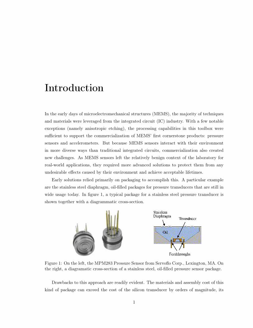
Early solutions relied primarily on packaging to accomplish this. A particular example
are the stainless steel diaphragm, oil-filled packages for pressure transducers that are still in
wide usage today. In figure 1, a typical package for a stainless steel pressure transducer is
shown together with a diagrammatic cross-section.
Figure 1: On the left, the MPM283 Pressure Sensor from Servoflo Corp., Lexington, MA. Onthe right, a diagramatic cross-section of a stainless steel, oil-filled pressure sensor package.
Drawbacks to this approach are readily evident. The materials and assembly cost of this
kind of package can exceed the cost of the silicon transducer by orders of magnitude, its
1

2
only function to isolate the sensor. It adds significant factors that must be addressed in the
design including the coefficient of thermal expansion (CTE) of the oil fill and the stresses in
the stamped, stainless steel diaphragm. The hermetic feedthroughs are also high risk points
of failure, particularly at higher pressures.
A significant motivation to develop more robust sensors is to lower the requirements and
cost of packaging for MEMS sensors to bring the cost of the package more in line with the
cost of the transducer. A second incentive is the evolution of transducer technology into
applications that interact with many different kinds of stimuli: light, chemicals (fluid and
gas), biological cells, extreme temperature, direct contact, radiation, etc. This has pushed
the need for materials and techniques that stand up to different conditions or have differ-
ent properties than can be accomplished with what was available for standard integrated
circuits. Examples are shown in Figure 2 illustrate high temperature, chemical and biologi-
cal applications. Techniques and materials to extend the operating environment of MEMS
sensors can also improve sensor lifetimes in existing applications as well as enable new ones
that would not otherwise be possible.
(a) (b) (c)
Figure 2: (a) A Fabry-Pérot pressure sensor [1](©IOP Publishing 2009), (b) a high tem-perature humidity sensor [2](©Elsevier 2009) , and (c) a biocompatible capacitive micro-machined ultrasonic transducer (CMUT) array [3] (©IOP Publishing 2007), reprinted withpermission.
The work presented here was done as two parts: the first focused on evaluation of
materials and development of processing techniques for PECVD silicon carbide and iridium,
the second on applications demonstration.

Chapter 1
Development of a Chemically Robust
Dielectric
Introduction
In a toolbox for designing environmentally hardened sensors, it is desireable to have a
dielectric that is relatively inert in a large range of chemistries. Popular dielectrics have
individual strengths, but none stand out as having remarkable robustness in an extraordinary
range of conditions. All variations of silicon dioxide (thermal, LPCVD, PECVD, spin-on-
glass (SOG)) etch quite readily in hydrofluoric acid. Silicon nitride in all of its forms, while
more resistant than oxides, also has finite, measureable etch rates in hydrofluoric acid [4].
Organics such as polyimide and bisbenzocyclobutene (BCB) have temperature limitations,
particularly in the presence of oxygen. They are also usually susceptible to degradation in
oxidizing chemistries such as sulfuric peroxide, solvents, or in some cases even water.
Polytetrafluoroethylene (PTFE) deposited by PECVD has shown some promise in this
area [5]. While this film does exhibit excellent chemical resistance, it has two drawbacks:
films of this material tend to be porous and they decompose at relatively low temperatures
(200 °C [6]). Many applications do not require operation near the decomposition tempera-
ture, but the limitation on further processing after deposition of the PTFE is a drawback.
Even photolithography singe temperatures of 150 °C can have an adverse affect on the film,
causing it to flow and deform. Furthermore, while the porosity can be a beneficial attribute,
as was demonstrated in a solid-state oxygen sensor [7], it is not desirable for an encapsulating
material that must protect the underlying substrate.
3
4 CHAPTER 1. DEVELOPMENT OF A CHEMICALLY ROBUST DIELECTRIC
1.1 Initial Selection
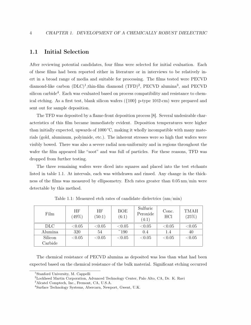
After reviewing potential candidates, four films were selected for initial evaluation. Each
of these films had been reported either in literature or in interviews to be relatively in-
ert in a broad range of media and suitable for processing. The films tested were PECVD
diamond-like carbon (DLC)1,thin-film diamond (TFD)2, PECVD alumina3, and PECVD
silicon carbide4. Each was evaluated based on process compatibility and resistance to chem-
ical etching. As a first test, blank silicon wafers (100 p-type 10W-cm) were prepared and
sent out for sample deposition.
The TFD was deposited by a flame-front deposition process [8]. Several undesirable char-
acteristics of this film became immediately evident. Deposition temperatures were higher
than initially expected, upwards of 1000 °C, making it wholly incompatible with many mate-
rials (gold, aluminum, polyimide, etc.). The inherent stresses were so high that wafers were
visibly bowed. There was also a severe radial non-uniformity and in regions throughout the
wafer the film appeared like “soot” and was full of particles. For these reasons, TFD was
dropped from further testing.
The three remaining wafers were diced into squares and placed into the test etchants
listed in table 1.1. At intervals, each was withdrawn and rinsed. Any change in the thick-
ness of the films was measured by ellipsometry. Etch rates greater than 0.05 nm/min were
detectable by this method.
Table 1.1: Measured etch rates of candidate dielectrics (nm/min)
Film HF(49%)
HF(50:1)
BOE(6:1)
SulfuricPeroxide(4:1)
Conc.HCl
TMAH(25%)
DLC <0.05 <0.05 <0.05 <0.05 <0.05 <0.05Alumina 320 54 ~190 0.4 1.4 40SiliconCarbide
<0.05 <0.05 <0.05 <0.05 <0.05 <0.05
The chemical resistance of PECVD alumina as deposited was less than what had been
expected based on the chemical resistance of the bulk material. Significant etching occurred
1Stanford University, M. Cappelli2Lockheed Martin Corporation, Advanced Technology Center, Palo Alto, CA, Dr. K. Ravi3Alcatel Comptech, Inc., Fremont, CA, U.S.A.4Surface Technology Systems, Abercarn, Newport, Gwent, U.K.

1.2. BACKGROUND OF PECVD SILICON CARBIDE 5
in all of the media tested, making it unsuitable for use as an encapsulation material for
environmentally hardened sensors. In discussions with Alcatel, the probable cause of this
unexpected reactivity was the deposition temperature. Typically the film is deposited at
600 °C. In this trial, the temperature had been lowered to 350 °C in an attempt to reduce
the stress below 500MPa and achieve CMOS compatibility. While exploration of process
conditions could potentially have led to acceptable results, further work was directed towards
the remaining two films.
In the next phase, DLC and PECVD carbide were deposited on a thin-film microelectrode
array discussed in Chapter 3 and shown in Figure 1.1.
Figure 1.1: Thin-film microelectrode array
It was at this point that a problem
with the DLC deposition process became
apparent. The process tested required a
relatively high-energy ion bombardment to
achieve the desired film properties, specifi-
cally the stabilization of the necessary sp3
carbon hybridization [9]. This had the un-
fortunate side effect of sputtering the sur-
face of the wafer. Sputtering was so severe
that the metal electrodes and traces were
almost completely removed. This had not
been evident from examining the surface of
bare wafers. As with the PECVD alumina,
a set of process parameters that would yield
a suitable DLC thin film could potentially
be found, but because ion bombardment
was not necessary for PECVD silicon car-
bide, further effort was directed exclusively
at the carbide.
1.2 Background of PECVD Silicon Carbide
As a point of nomenclature, crystalline, stoichiometric SiC will be referred to by its chemical
formula. PECVD silicon carbide, amorphous silicon carbide, carbide, or α-SiC:H all refer to

6 CHAPTER 1. DEVELOPMENT OF A CHEMICALLY ROBUST DIELECTRIC
α-SixC1−x:H. Before pressing forward into the study of PECVD silicon carbide, it is worth
reviewing the history of the material. Before methods of controlled plasma deposition were
developed, amorphous silicon carbide was deposited by pyrolitic methods which relied on the
combustion of reactants to generate the desired product [10]. The earliest reference found
on the deposition of silicon carbide by radio frequency plasma was by Sterling and Swann in
1965 [11]. At this time, PECVD deposition was referred to as the “glow discharge” method
of deposition. Silane and methane in helium were reacted to deposit a film that, like the
crystalline SiC films, showed a strong absorption peak at 12.6mm [12]. A more detailed
examination was done in 1977 by Anderson and Spear [13]. They made the first attempt to
analytically characterize the nature of PECVD silicon carbide by looking at stoichiometry,
optical band gap, and conductivity. In doing so, they were the first to reveal the complex
chemical and electronic character of the film.
Several aspects of PECVD silicon carbide are responsible for the complexity of its prop-
erties:
• Variable stoichiometry of deposited films: Stoichiometry can be tuned by process
conditions from amorphous silicon to amorphous carbon [14,15].
• Bond stoichiometry: For a given stoichiometry of α-SixC1−x:H there exist different
permutations of Si-C, Si-Si, and C-C bonds which satisfy that formula. Consequently
two films of identical stoichiometry can have different properties (conductivity, chem-
ical reactivity, etc.).
• Electronic properties of carbon: Carbon can bond either graphitically (sp2) or
tetrahedrally (sp3). As part of a Si-C matrix, carbon is almost always bound tetra-
hedrally. Process conditions and carbon concentrations, however, can create localized
regions of C-C graphitic bonds. The mechanical and electrical properties of these
bonds are very different. Consequently a change in the hybridization of carbon can
greatly affect film properties [13].
• Hydrogen content: The amount of terminating hydrogen bound into the silicon
carbide matrix can vary greatly up to an atomic percentage of more than 50% [14].
The range of conditions possible for a PECVD deposition influences each of these factors.
Consequently, the range of films from a typical PECVD silicon carbide process spans a
continuum of possibilities: hard to soft, insulator to semiconductor, chemically resistant to

1.2. BACKGROUND OF PECVD SILICON CARBIDE 7
moderately reactive. For this reason, the development of a PECVD carbide process requires
careful film analysis and testing to ensure that the film has the desired properties. It is also
why the development process is unique to every deposition system and configuration.
1.2.1 Precursors
While this work focused on the plasma reaction of silane and methane in argon as an inert
carrier, other precursors have been used. Silane has been used almost exclusively as a source
of silicon for a two-gas precursor system. A more diverse list of gases such as ethane (C2H6),
ethylene (C2H4), acetylene (C2H2), and butane (C4H10) have all been used as sources of
carbon [13,15–17]. The amount of carbon incorporated into the film and the deposition rate
is higher per molar volume for the less saturated precursors. This would be expected for
the energy of activation (radical formation) of acetylene (1.8 eV), ethylene (2.7 eV), ethane
(3.6 eV), and methane (4.3 eV).
PECVD silicon carbide has also been deposited using a single source precursor. Chiu and
Huang demonstrated the use of dodecamethylcyclohexasilane ((CH3)2Si)6, though at a
higher temperature than is typical for a PECVD process (1000 °C) [18]. Hexamethydisilane
(CH3)6Si2 [19], trimethylsilane (CH3)3SiH [20, 21], and 1,3-disilabutane [22] have also
been used. Processes with single precursors typically achieved deposition rates several times
higher than what was achieved with silane-organic mixtures, on the order of several tens
of nm/min. The stoichiometry of the films from trimethylsilane also tended to be carbon-
rich. This is different from films made using a silane-methane recipe. These tend toward
a silicon-rich stoichiometry, owing to the difference in bond energies between methane and
silane (98.8 kcal/mole vs. 70.9 kcal/mole) [23].
Another method of depositing α-SixC1−x:H which warrants mention is that of reactive
sputter deposition [24]. In this method, a silicon target is sputtered in the presence of
methane and argon. Results from Fourier transform infra-red (FTIR), ultraviolet (UV),
visible, near-infrared (NIR), and photoacoustical spectroscopy (PAS) showed that films pro-
duced in this manner were more disordered and inhomogeneous than the PECVD counter-
part. Among other differences in properties, this lead to a higher conductivity, which would
make it less desirable as a dielectric encapsulating layer.

8 CHAPTER 1. DEVELOPMENT OF A CHEMICALLY ROBUST DIELECTRIC
1.2.2 Electrical and Optical Properties
The resistivity of PECVD silicon carbide has been measured under a variety of conditions.
Tyczkowskiet et al. [25] measured the temperature dependence of D.C. conductivity of films
produced from tetramethylsilane. Room temperature resistivity varied between 2x10¹⁴ and
1.5 x 10¹⁶ W-cm. Resistivity variations due to process conditions were measured across nearly
four orders of magnitude by Chattopadhyay et al. [26]: from 2x10⁹ to 6x10¹² W-cm. The
conductivity of carbide can also be altered by doping. When phosphine (PH3) was added
to a silane/ethylene deposition to produce n+ a-SiC:H, the conductivity increased from
2.2x10⁻¹² S/cm for the undoped films to 2.8x10⁻³ S/cm [27].
Because of its potential for use in optical applications, the photoconductivity of PECVD
silicon carbide has been characterized [28]. The conductivity of carbide films illuminated
with a 50mw/cm2 white light source increased roughly four orders of magnitude. Dark con-
ductivity and photoconductivity both decrease with increasing carbon content. This trend
has been shown to continue for higher percentage carbon films, suggesting that increased
carbon content reduces generated carrier lifetimes and/or mobility.
The optical band gap (Eopt) of carbide has been investigated by a number of sources,
owing to the interest for its use in photovoltaic cells and other optical applications. The
optical band gap itself is not a well defined value, although it is referred to quite extensively
because of it usefulness in evaluating a materials optical performance. It has no physical
basis. Two definitions for Eopt have been found. The first is that point where the absorption
coefficient reaches 106m-1. The second, and that quoted more often is that determined from
the Tauc relationship
αhv = B (hv − Eopt)n (1.1)
where α is the absorption coefficient, hv is the photon energy, B is a proportionality constant,
and n a parameter corresponding to the density of states. Eopt is most often determined by
extrapolating a linearization of ((αhv)1n vs. hv and taking Eopt as the x-axis intercept [25].
The value obtained is dependent on the choice of n as the density of states. The majority
of sources use n = 2 for a-SixC1-x:H, though Tyczkowski et al. claim a better fit for higher
temperature films using n = 3. Values of the optical band gap for a-Si:H is 1.75 eV and for a-
C:H is 4 eV. As might be expected, the values for a-SixC1-x:H have been reported from 1.5 to
3.0 eV [13,15,26]. Several investigators have confirmed the linear dependence of the optical

1.2. BACKGROUND OF PECVD SILICON CARBIDE 9
band gap on x between 0.8 and 0.38 with a maximum near 3 eV at x = 0.38 [14, 16, 28].
Transmission as high as 60% down to 500 nm has been reported [29].
Values reported throughout the literature for the refractive index vary greatly, from 3.3
(silicon rich films) to 1.4. Nearly that same broad range of refractive indices were observed
in this work. An inverse relationship was found between the carbon atomic percentage and
the refractive index. This relationship is roughly linear at lower carbon concentrations,
up to roughly 30%, where it levels off and nf approaches 1.75 [14, 15, 26, 28]. It should be
noted, however, that the refractive index is not solely dependent on the percentage of carbon
alone. For a-Si0.75C0.25:H, Sussman and Ogden reported nf of roughly 2.4. That reported
by Kuhman et al. was roughly 1.9. Catherine et al. reported a variation from 2.2 to 2.5 with
deposition temperature for x=0.6. For films produced from hexamethyldisilane (HMDS),
Klumpp et al. reported an increase in refractive index with deposition temperature, from
2.48 to 2.65 at 200 °C and 300 °C respectively [19]. This trend was confirmed by He et
al. [29].
1.2.3 Mechanical Properties
In 1994, Khakani et al. compared the mechanical properties of PECVD silicon carbide with
that of SiC deposited by both laser ablation (LAD) and triode sputtering (TSD) [30]. They
found that the hardness of the PECVD films decreases in films where the C:Si ratio is less
than 1:1. Using FTIR, they were able to establish a direct correlation between the Si-C
bond density and both hardness and Young’s modulus. As is discussed in Section 1.3.3.2,
FTIR examination of the Si-C bond density can also provide a key to understanding the
chemical reactivity of PECVD silicon carbide in alkaline solutions. Additionally, it was
found that for films with an identical 1:1 Si:C stoichiometry, hydrogenation decreased the
hardness of the PECVD films (19.2GPa) relative to the non-hydrogenated LAD (30.6GPa)
and TSD (28.1GPa). Other work has shown that hardness increases with the radio frequency
power of deposition [29]. This tends to correlate with increasing carbon percentage, which
corresponds with the previous observation.
Because of interest for its use as a wear resistant coating, abrasion tests have been done
on deposited films. In an abrasion test, a calibrated abrasive is applied to the surface under
test and either weight loss or thickness loss is measured over time. While it is difficult to
correlate data from different tests and conditions, carbide has demonstrated a wear resistance
roughly 22 times greater than that of Corning 7059 B glass [29].

10 CHAPTER 1. DEVELOPMENT OF A CHEMICALLY ROBUST DIELECTRIC
The density of deposited films can vary significantly. Sussman and Ogden reported higher
densities of 2.5 g/cm3 for silicon-rich films (x=0.8 ) compared with 2.0 g/cm3 for carbon rich
films (x=0.2) [28]. Their analysis, however, did not take into account the percentage of
hydrogen in the film, which can influence the resulting density greatly.
The stresses reported in as-deposited films are predominantly compressive. The magni-
tude ranged across the board from the low stress reported by Tong et al. of -34MPa [31] to
the high stress reported by Jeanet al. of -1,400MPa [23]. As discussed in more detail below,
stress can be altered greatly by annealing. Tensile stress, however, has been reported, both
in this work (430MPa) and in that by Loboda et al. (200MPa) [20].
1.2.4 Chemical Properties
As demonstrated in the screening process, PECVD silicon carbide is relatively unreactive in
many environments. It is not, however, impervious. Several papers characterize the etch be-
havior of carbide, though typically it is under extreme conditions. Tong et al. characterized
the etch rate in 49% HF of carbide produced under various conditions. They demonstrated
that the etch rate correlated inversely with the refractive index of various films. Low refrac-
tive index films (2.0) etched at 48 nm/min. Higher index films (2.3) etched at one fourth
that rate. Films produced by another source using HMDS, however, had undetectable etch
rates in both room temperature 48% HF (hydrofluoric acid) and in 33% KOH (potassium
hydroxide) at 80 °C [19]. Resistance to KOH was demonstrated by Jean et al. when they
fabricated PECVD silicon carbide membranes by etching through the wafer in a 30% KOH
solution at 80 °C. By depositing carbide on the both sides of the wafer, they were able to
use it both as the membrane material and as the etch mask.
An examination of failure mechanisms in thermal ink jet heads showed that carbide
is etched in alkaline solutions under repeated thermal cycling. The temperature of the
thermal cycle was 300 °C. The etch rate increased dramatically above pH11. Data from the
trial supports the conclusion that the mechanism of etching was one of SiO2 formation and
dissolution, facilitated by the high temperature [32].
Nodules have been observed by tunneling electron microscopy (TEM) in films deposited
at lower powers. Analysis by selected area diffraction showed these nodules to be carbon,
and attributed to plasma-phase polymerization of methane. Nodules were not observed in
higher power depositions. The theory put forth was that higher powers favored the ion-based
reactions near the deposition surface rather than the radical-based polymerization, which

1.2. BACKGROUND OF PECVD SILICON CARBIDE 11
occurs in plasma. Deposition temperature had an effect only on the size of the nodules; it
did not eradicate them. This was consistent with their hypothesis, as substrate temperature
would not have a significant impact on the plasma reaction [29].
Flourine-based plasmas can be used to pattern PECVD silicon carbide. Carbide can be
patterned using CF4, SF6, and CHF3/O2 using conventional photoresist as a mask [19].
1.2.5 Annealing
In numerous works, annealing PECVD silicon carbide can cause significant changes in the
character of the film. As a carbide film is annealed beyond its deposition temperature,
hydrogen is released, densifying the film and increasing the refractive index. As the annealing
temperature increases, hydrogen atoms bound to alkyl groups are released first, followed by
those bound to silicon. Evolution and densification continues until about 650 °C, after which
no hydrogen can be detected in the film by IR. Densification can cause as much as a 70%
decrease in film thickness under certain conditions [19,25,33]. The density of Si-C bonding
also increases, in one case by an order of magnitude when annealed at 1200 °C [34].
At 800 °C, the film begins to become to develop a microcrystalline structure. The size of
the crystallites increases with temperature until at 1200 °C, the film becomes polycrystalline
[34]. This is consistent with results reported elsewhere that plasma depositions at 1000 °C
are crystalline, showing patterns by X-ray diffraction like that of β-SiC [18].
Annealing has consistently been shown to shift mechanical stress towards the tensile
regime. Most carbide films are compressive (sometimes very compressive) as deposited, and
proper annealing can lead to a zero-stress film. In one experiment, rapid thermal annealing
(RTA) for 400 sec at 600 °C was shown to reduce the stress from -1,100MPa (compressive)
in the film as deposited to roughly zero. Further annealing for 800 sec resulted in a slightly
tensile film [23]. Klumpp et al. were also able to achieve a near-zero stress film after annealing
in a furnace for 12 h at 450 °C. Anneals at 600 °C and at 1000 °C produced successively more
tensile films, in one extreme case as much as 1,750MPa tensile [19]. Other examples that
demonstrate the shift towards tensile stress have been reported [33].
1.2.6 Applications
One of the earliest and most pervasive applications of PECVD silicon carbide has been in ink
jet devices. It is typically used as a coating in the fluidic channel of thermal ink jet heads to

12 CHAPTER 1. DEVELOPMENT OF A CHEMICALLY ROBUST DIELECTRIC
protect the resistive heating elements from the corrosive effects of the ink [32,35,36]. Early
ink jet heads were often made from silicon and glass [36]. Research to address the corrosion
resistance in alkaline ink chemistries dates back to the early days of this application [37,38].
Because of its large optical gap, PECVD silicon carbide has been used to fabricate thin-
film, light-emitting diodes (TFLED). Electroluminscence in a p-i-n a-SiC TFLED is in the
visible wavelength region. Because Eopt can be adjusted by process conditions, TFLED’s
can be fabricated with colors ranging from red to yellow [39]. The wide optical band gap also
makes PECVD silicon carbide suitable for use as a window layer in a photovoltaic cell [15].
Low-leakage, high-gain a-SiC:H/a-Si:H p-i-n heterostructure photodetectors have been
demonstrated [27, 40]. A representation of the one by Dutta et al. is shown in Figure 1.2.
The intrinsic carbide layer serves as an insulator to lower leakage current and provides a
high-field region for avalanche multiplication of photogenerated carriers. Taking advantage
of the larger optical gap of carbide (2.35 eV in this case) enabled a quantum efficiency greater
than unity with a leakage current less than 10 nA/cm2 and a photocurrent multiplication of
9.
Figure 1.2: α-SiC:H photodetector, afterDutta et al. [27]
Because PECVD silicon carbide has a higher
coordination number than PECVD silicon ni-
tride, thin-film transistors (TFT’s) made with a
carbide gate have superior transport properties.
Gates made with PECVD nitride, however, are a
superior insulator (lower leakage), have a greater
εr, and break down at a higher voltage than
those of carbide. TFTs made with a laminated
a-SixC1-x:H/a-SiyN1-y gate show a two-fold in-
crease in transconductance due to the decrease
in interfacial defects, while preserving the supe-
rior qualities of a single-layer nitride gate [41].
Jean et al. successfully demonstrated the use
of a carbide membrane as a mask for X-ray
lithography [23]. As described previously, the low stresses necessary for membrane fab-
rication were achieved by RTA.
Because SiC is one of the harder, more wear resistant compounds available, work has
been done exploring the use of PECVD silicon carbide as a lower temperature coating for

1.3. DEVELOPMENT OF A PECVD SILICON CARBIDE PROCESS 13
mechanical protection. While some processes do produce relatively hard carbide layers, none
approach the mechanical resistance of crystalline or polycrystalline SiC.
In fabrication, the chemical resistance of carbide makes it an ideal masking layer. It
has been used during backside etches in the fabrication of microfluidic pumps and pressure
sensors [19]. It was also used in the formation thermally-isolated bridges for the fabrication
of a thin-film bolometer [42]. Because of its resistance to HF, free-standing carbide structures
can be fabricated in a surface micromachining process using silicon dioxide as a sacrificial
layer [31].
A selection of film properties pulled from the literature are summarized in table 1.2.
Table 1.2: Properties of α-SixC1-x:H
Property Value CommentDensity (g/cm3) 2.4 [23]
1.75 [34]2.1 [26]
x≈0.5
Index of Refraction 2.0 - 2.4 [31]1.79 - 2.37 [21]
Trimethylsilane
Dielectric Constant 4.13 - 6.28 [21] TrimethylsilaneOptical band Gap (eV) 2.0 - 2.6 [39]Resistivity (Ω- cm) 106- 1012 [13] Temperature and
stoichiometric dependentStress as Deposited (MPa) -1,400 to -300 [23]
-30 to -64 [31]-200 to +100 [21]
0.25 < x < 0.8
Coefficient of ThermalExpansion (ppm)
3.3 [33]
Hardness (GPa) 10.8-19.5 [25],17 [43]
x=0.5 - 0.67
Young’s Modulus 88 10, 154 16 [25], 100 17 [44] x=0.67x=0.5
Poisson’s Ratio 0.29 0.16, 0.23 0.11 [25] x=0.67x=0.5
1.3 Development of a PECVD Silicon Carbide Process
Development of an in-house carbide process was done in two phases. In the first phase,
process parameters were sought such that the resulting film satisfied the criteria for use in
14 CHAPTER 1. DEVELOPMENT OF A CHEMICALLY ROBUST DIELECTRIC
a range of micromachined structures. The most useful film would be
• low stress as deposited,
• resistant to wet etchants,
• highly resistive,
• patternable, and
• conformal.
In the second phase, further investigation was carried out on the chemical, physical, and
electrical properties of a subset of these films.
1.3.1 Parameter Determination
The initial samples of silicon carbide that were evaluated in the dielectric screening were
prepared by Surface Technology Systems, (STS Ltd., Wales, UK) using their Multiplex CVD
system with a 380 kHz power supply. Deposition parameters used were 600mTorr, 10 sccm
SiH4, 250 sccm CH4, 300 sccm Ar, 300 °C, and a power level of 60W. The remainder of
the work was carried out using a modified STS 310PC PECVD deposition system at Stan-
ford University. Two RF power supplies were used in a switched mode, a high frequency
(13.5MHz) unit and low frequency (187 kHz) unit. The system was plumbed with 2% SiH4
in Ar, CH4and purged with Ar. Switching the carrier case for the silane (2% SiH4) from
nitrogen to argon was done to avoid the possibility of forming a carbide-nitride hybride
(which might bear investigation in its own right). The electrode area was 730 cm2. With
two exceptions, all films were deposited using a dual frequency, switched plasma technique
based on prior success using this method to control the stress in PECVD silicon nitride.
Two additional trials were done with constant low frequency and constant high frequency
excitation. All films were deposited at 350 °C. Before discussing the optimization process,
however, it is essential to establish that results apply strictly to the STS310 PC PECVD
deposition system. While the work here describes what is believed to be an optimal PECVD
silicon carbide film for use in environmentally hardened transducers for that system, many
other systems have greater degrees of freedom in their process variables (electrode spac-
ing, DC bias, electrode symmetry, frequency adjustment, temperature >350 °C, methods of
excitation, precursor selection, etc.). This greater parameter space effects both the opti-
mization process and the resulting film properties. It is also not implied that the carbide

1.3. DEVELOPMENT OF A PECVD SILICON CARBIDE PROCESS 15
films produced in this work are optimal for the material; merely that they are optimal given
the technical resources of the available deposition system. Together with the greater pro-
cess control in different deposition systems; broader range of precursor choices; and newer
plasma technologies, such as electron cyclotron resonance (ECR), inductively coupled plas-
mas (ICP), and triode configured systems superior quality films are undoubtedly possible.
The process development of PECVD silicon carbide began by establishing the range
of deposition parameters. Those used are listed in Table 1.3. The pressure range was
chosen because preliminary trials showed that higher pressures tended towards lower stress
films. The upper pressure was a limitation of the pumping capabilities of the machine.
Temperature was fixed at the system maximum and the upper bound of CMOS compatibility.
As described earlier, higher temperature films tended to have higher level of Si-C bonding.
The flow rate of 2% SiH4 in argon was fixed at the system maximum as this had been shown
to yield maximum uniformity across the platen. Power parameters were bound on the low
end by the minimum required for detectable deposition (50W) and on the upper end by
the system power supplies (150W). The period of excitation was bound by that required
to achieve a steady state plasma (2 s) and that required to deposit a monolayer (7 s). The
latter boundary ensured the deposition of a homogeneous film rather than a laminate. A
switched frequency method of deposition was chosen because of previous success depositing
a low-stress PECVD silicon nitride. A complete list of process conditions and results of film
properties can be found in Appendix A. The parameters for the “best” film produced are
also shown in Table 1.3.
Table 1.3: Process parameter space for PECVD silicon carbide process development
Parameter Range SelectedPressure (mTorr) 1000 - 1600 1600Temperature (°C) 350 (Fixed) 350
2% SiH4Flow Rate (sccm) 2840 (Fixed) 2840CH4Flow Rate (sccm) 360, 900, 1440 1440Hi Freq. Power (W) 50, 100, 150 100Hi Freq. Period (s) 2 -7 4.5
Low Freq. Power (W) 50, 100, 150 100Low Freq. Period (s) 2 -7 4.5
During deposition, a substantial layer of particles accumulated on the sidewalls of the
chamber and, in particular, under the platen. This is not the case with either the PECVD

16 CHAPTER 1. DEVELOPMENT OF A CHEMICALLY ROBUST DIELECTRIC
silicon nitride or the PECVD silicon dioxide processes run in the same chamber. However,
no particles were visible on the platen itself or on the wafers. Analysis of the powder-like
substance by FTIR revealed strong Si-H stretching with little evidence of carbon bonding,
It was also observed that this “silanacious dust” was pyrophoric, and on occasion would
spontaneously react with the air upon chamber venting. This level of particle generation in
a carbide process is consistent with results reported elsewhere [21]. In addition to concern
about pinhole problems in the film, it raises a potential concern for vacuum pump operation.
In-line filters were already being used in the system and examination of the pump did
not reveal any accumulation of deposits. By lowering the pressure to 1,200mTorr, a set
of process parameters were found that could also produce a good quality, low-stress film
while decreasing the amount of particulate accumulation in the chamber. This adjustment
reduced, but did not eliminate, the amount of particle deposition. As a result, total chamber
accumulation was limited to 2 mm before an etchback cleaning cycle.
1.3.2 Thin-film Characterization
1.3.2.1 Optical Properties
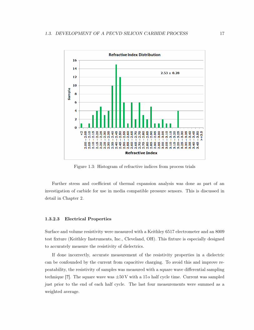
As mentioned previously, the refractive index of carbide has a broad range. Values in this
work measured by ellipsometry ranged from 1.8 to 3.2. An average value of those films
produced during the process development phase was 2.53 ± 0.28. The distribution of all
films from the trial can be seen in Figure 1.3. Even after fixing the deposition conditions
on a set of parameters that produces a film of desirable characteristics, the refractive index
tended to increase under those same process conditions as the thickness of the deposited
film increased.
1.3.2.2 Mechanical Properties
Stress was measured with an SMSI 3800 stress gauge (Scientific Measurement Systems, Inc.,
San Jose, CA) using wafers for which reference measurements had been made. Extremes
of stress measured between -401MPa (compressive) and 431MPa (tensile). Films tended
to be slightly compressive, averaging around -96MPa. It was possible to determine a set
of parameters that could consistently produce films with stresses lower in magnitude than
-30MPa. As with the refractive index, the stress distribution had a broad range of values
as shown in Figure 1.4.
1.3. DEVELOPMENT OF A PECVD SILICON CARBIDE PROCESS 17
Figure 1.3: Histogram of refractive indices from process trials
Further stress and coefficient of thermal expansion analysis was done as part of an
investigation of carbide for use in media compatible pressure sensors. This is discussed in
detail in Chapter 2.
1.3.2.3 Electrical Properties
Surface and volume resistivity were measured with a Keithley 6517 electrometer and an 8009
test fixture (Keithley Instruments, Inc., Cleveland, OH). This fixture is especially designed
to accurately measure the resistivity of dielectrics.
If done incorrectly, accurate measurement of the resistivity properties in a dielectric
can be confounded by the current from capacitive charging. To avoid this and improve re-
peatability, the resistivity of samples was measured with a square wave differential sampling
technique [?]. The square wave was ±50V with a 15 s half cycle time. Current was sampled
just prior to the end of each half cycle. The last four measurements were summed as a
weighted average.

18 CHAPTER 1. DEVELOPMENT OF A CHEMICALLY ROBUST DIELECTRIC
Figure 1.4: Histogram of stress from process trials
(a) Volume Resistivity (b) Surface Resistivity
Figure 1.5: Configuration of Keithley 8009 resistivity test fixture for (a) volume and (b)surface resistivity measurements
Iavg =I1 − 3I2 + 3I3 − I4
8(1.2)
A minimum of seven measurements were made for each sample. Wafers were baked for
1 hour at 140 °C prior to measurement to remove surface moisture. Volume resistivity was
1.3. DEVELOPMENT OF A PECVD SILICON CARBIDE PROCESS 19
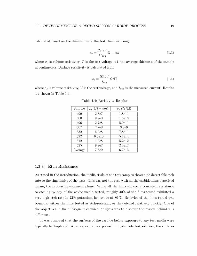
calculated based on the dimensions of the test chamber using
ρv =22.9V
tIavgΩ − cm (1.3)
where ρv is volume resistivity, V is the test voltage, t is the average thickness of the sample
in centimeters. Surface resistivity is calculated from
ρs =53.4V
IavgΩ/ (1.4)
where ρs is volume resistivity, V is the test voltage, and Iavg is the measured current. Results
are shown in Table 1.4.
Table 1.4: Resistivity Results
Sample ρv (Ω − cm) ρs (Ω/)499 2.8e7 1.8e11500 9.9e8 1.5e13496 2.7e8 5.0e11507 2.2e8 3.8e9532 6.9e8 7.8e11522 6.0e10 5.1e14512 1.0e8 5.2e12525 9.2e7 2.1e12
Average 7.8e9 6.7e13
1.3.3 Etch Resistance
As stated in the introduction, the media trials of the test samples showed no detectable etch
rate to the time limits of the tests. This was not the case with all the carbide films deposited
during the process development phase. While all the films showed a consistent resistance
to etching by any of the acidic media tested, roughly 40% of the films tested exhibited a
very high etch rate in 22% potassium hydroxide at 80 °C. Behavior of the films tested was
bi-modal; either the films tested as etch-resistant, or they etched relatively quickly. One of
the objectives in the subsequent chemical analysis was to discover the reason behind this
difference.
It was observed that the surfaces of the carbide before exposure to any test media were
typically hydrophobic. After exposure to a potassium hydroxide test solution, the surfaces
20 CHAPTER 1. DEVELOPMENT OF A CHEMICALLY ROBUST DIELECTRIC
were consistently hydrophylic. This is most likely due to the formation of a surface layer of
silicon dioxide, as has been previously reported [31]
1.3.3.1 Stoichiometry
The etch behavior indicates that there is some critical aspect in the chemistry of PECVD
silicon carbide that leads to its susceptibility to etching in solutions of KOH. As a first step,
the stoichiometries of representative samples were analyzed by Rutherford backscattering
(RBS) and hydrogen forward scattering (HFS) spectroscopy at Charles Evans and Associates
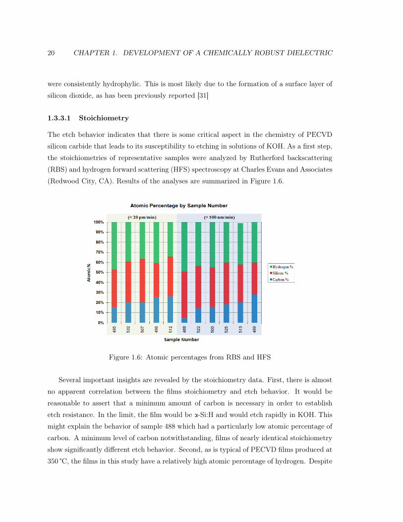
(Redwood City, CA). Results of the analyses are summarized in Figure 1.6.
Figure 1.6: Atomic percentages from RBS and HFS
Several important insights are revealed by the stoichiometry data. First, there is almost
no apparent correlation between the films stoichiometry and etch behavior. It would be
reasonable to assert that a minimum amount of carbon is necessary in order to establish
etch resistance. In the limit, the film would be a-Si:H and would etch rapidly in KOH. This
might explain the behavior of sample 488 which had a particularly low atomic percentage of
carbon. A minimum level of carbon notwithstanding, films of nearly identical stoichiometry
show significantly different etch behavior. Second, as is typical of PECVD films produced at
350 °C, the films in this study have a relatively high atomic percentage of hydrogen. Despite
1.3. DEVELOPMENT OF A PECVD SILICON CARBIDE PROCESS 21
the fact that some films are nearly 50% hydrogen, this also does not correlate with etch
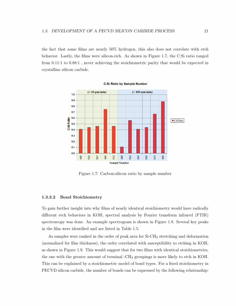
behavior. Lastly, the films were silicon-rich. As shown in Figure 1.7, the C:Si ratio ranged
from 0.11:1 to 0.88:1 , never achieving the stoichiometric parity that would be expected in
crystalline silicon carbide.
Figure 1.7: Carbon:silicon ratio by sample number
1.3.3.2 Bond Stoichiometry
To gain further insight into why films of nearly identical stoichiometry would have radically
different etch behaviors in KOH, spectral analysis by Fourier transform infrared (FTIR)
spectroscopy was done. An example spectrogram is shown in Figure 1.8. Several key peaks
in the film were identified and are listed in Table 1.5.
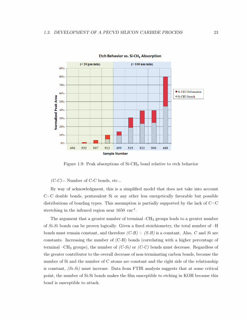
As samples were ranked in the order of peak area for Si-CH3 stretching and deformation
(normalized for film thickness), the order correlated with susceptibility to etching in KOH,
as shown in Figure 1.9. This would suggest that for two films with identical stoichiometries,
the one with the greater amount of terminal -CH3 groupings is more likely to etch in KOH.
This can be explained by a stoichiometric model of bond types. For a fixed stoichiometry in
PECVD silicon carbide, the number of bonds can be expressed by the following relationship:

22 CHAPTER 1. DEVELOPMENT OF A CHEMICALLY ROBUST DIELECTRIC
Figure 1.8: FTIR spectrogram of sample 488
Table 1.5: FTIR peak locations for PECVD silicon carbide
Peak Location (cm-1) Description700 - 800 Si-C stretching, SiCH3rocking or wagging970 - 1020 Si-CH2stretching
& 1250 -CH3symmetric deformation
& 2100 Si-H stretching2887 -CH3asymmetric stretch2949 -CH3symmetric stretch
4C = (C −H) + 2(C − C) + (Si− C)
4Si = (S −H) + 2(Si− Si) + (Si− C)
4C + 4Si = (C −H) + (S −H) + 2(Si− C) + 2(C − C) + 2(Si− Si) (1.5)
Where
C = Number of Carbon Atoms
Si = Number of Silicon Atoms
(Si-C) = Number of Si-C bonds
1.3. DEVELOPMENT OF A PECVD SILICON CARBIDE PROCESS 23
Figure 1.9: Peak absorptions of Si-CH3 bond relative to etch behavior
(C-C)= Number of C-C bonds, etc...
By way of acknowledgment, this is a simplified model that does not take into account
C=C double bonds, pentavalent Si or any other less energetically favorable but possible
distributions of bonding types. This assumption is partially supported by the lack of C=C
stretching in the infrared region near 1650 cm-1.
The argument that a greater number of terminal -CH3 groups leads to a greater number
of Si-Si bonds can be proven logically. Given a fixed stoichiometry, the total number of –H
bonds must remain constant, and therefore (C-H) + (S-H) is a constant. Also, C and Si are
constants. Increasing the number of (C-H) bonds (correlating with a higher percentage of
terminal –CH3 groups), the number of (C-Si) or (C-C) bonds must decrease. Regardless of
the greater contributor to the overall decrease of non-terminating carbon bonds, because the
number of Si and the number of C atoms are constant and the right side of the relationship
is constant, (Si-Si) must increase. Data from FTIR analysis suggests that at some critical
point, the number of Si-Si bonds makes the film susceptible to etching in KOH because this
bond is susceptible to attack.

24 CHAPTER 1. DEVELOPMENT OF A CHEMICALLY ROBUST DIELECTRIC
Isomers of silicon carbide are shown in Figure 1.10. It is easy to see how an increase in
terminal -CH3 groups can lead to an increase in Si-Si bonds which are susceptible to attack
by KOH.
(a) Isomer with terminal -CH3. 1 Si-C bond, 1Si-Si bond
(b) Isomer with no terminal -CH3. 0 Si-Sibonds, 1 Si-C bond
Figure 1.10: Isomers of silicon carbide
Interesting to note is that films prepared by Tawada et al. with an ethylene precursor
showed none of the peaks for a terminal -CH3 group. This would seem to indicate that
ethylene might be a superior precursor where the chemical resistance of carbide were of
tantamount concern [15].
1.4 Thin Film Comparisons
1.4.1 Comparison with Silicon Carbide
The majority of literature on deposition processes for silicon carbide focuses on CVD pro-
cesses for the crystalline or polycrystalline form, and its use as a semiconductor for high
temperature electronics, light emitting diodes, mechanical barriers, and other applications.
That research tends to focus on the electrical properties of SiC, particularly at higher tem-
peratures. The operating temperature limit of conventional silicon electronics is limited in
range from 200 to 250 °C depending on the particular technology. This limitation is a result
of silicon’s intrinsic carrier concentration and band gap (1010 cm-3 and 1.11 eV [45]). The
particular crystal forms 6H-SiC and 4H-SiC have much lower intrinsic carrier concentra-
tions (10-6 and 10-10 cm-3 [46]) and higher band gaps (3.02 and 3.26 eV [47]). This has the
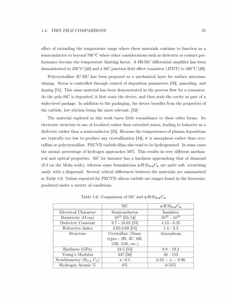
1.4. THIN FILM COMPARISONS 25
effect of extending the temperature range where these materials continue to function as a
semiconductor to beyond 700 °C where other considerations such as dielectric or contact per-
formance become the temperature limiting factor. A 6H-SiC differential amplifier has been
demonstrated to 450 °C [48] and a SiC junction field effect transistor (JFET) to 500 °C [49].
Polycrystalline 3C-SiC has been proposed as a mechanical layer for surface microma-
chining. Stress is controlled through control of deposition parameters [50], annealing, and
doping [51]. This same material has been demonstrated in the process flow for a resonator.
As the poly-SiC is deposited, it first coats the device, and then seals the cavity as part of a
wafer-level package. In addition to the packaging, the device benefits from the properties of
the carbide, low stiction being the most relevant. [52]
The material explored in this work bares little resemblance to these other forms. Its
electronic structure is one of localized rather than extended states, leading to behavior as a
dielectric rather than a semiconductor [25]. Because the temperatures of plasma depositions
are typically too low to produce any crystallization [34], it is amorphous rather than crys-
talline or polycrystalline. PECVD carbide films also tend to be hydrogenated. In some cases
the atomic percentage of hydrogen approaches 50%. This results in very different mechan-
ical and optical properties. SiC for instance has a hardness approaching that of diamond
(9.3 on the Mohs scale), whereas some formulations a-H:Si1-xCx are quite soft, scratching
easily with a fingernail. Several critical differences between the materials are summarized
in Table 1.6. Values reported for PECVD silicon carbide are ranges found in the literature,
produced under a variety of conditions.
Table 1.6: Comparison of SiC and a-H:Si1-xCx
SiC a-H:Si1-xCx
Electrical Character Semiconductor InsulatorResistivity (W-cm) 1011 [53, 54] 1010 - 1016
Dielectric Constant 9.7 - 10.03 [55] 4.13 - 6.25Refractive Index 2.65-2.69 [55] 1.4 - 3.3
Structure Crystalline (Manytypes - 2H, 3C, 6H,15R, 21R, etc.)
Amorphous
Hardness (GPa) 24.5 [55] 8.8 - 19.2Young’s Modulus 447 [56] 56 - 153
Stoichiometry (Si1-x Cx) x=0.5 0.33 < x < 0.90Hydrogen Atomic % 0% 0-55%

26 CHAPTER 1. DEVELOPMENT OF A CHEMICALLY ROBUST DIELECTRIC
1.4.2 LPCVD Silicon Nitride with PECVD Silicon Nitride
As a point of interest, Table 1.7 compares some literature values for SiN and its PECVD
counterpart, α-SiNx:Hy. Like the carbides, the change from crystalline to amorphous with
the addition of hydrogen affects several properties in a similar way: reduced dielectric con-
stant, lower hardness, and a reduced Young’s modulus.
Table 1.7: Comparison of LPCVD SiN and PECVD α-SiCx:Hy
SiN PECVD SiNElectrical Character Insulator InsulatorResistivity (W-cm) >1015 [57] 1.21x10⁷-
2.06x10¹² [58]2x10¹⁴ [59]
2x10¹⁴-≥ 1016 [60]Dielectric Constant 6.7-7 [61] 4.64 [61]
5.4-6.6 [58]5.4-6.2 [60]
Refractive Index 1.95-2.02 [61]1.98-2.02 [62]
1.98 [63]
2.14 [61]1.85-3.2 [58]
Structure Crystalline (3 types -a,b,g)
Amorphous
Hardness (GPa) 21.0 ± 0.9 [64] 10-12 [65]Young’s Modulus (GPa) 193-310 [66]
222 ± 3 [64]90-130 [65] [67]
Poisson’s Ratio 0.23 ± 0.02 [68]0.28 ± 0.05 [64]
0.25optimization [69]0.23 ± 0.02,
0.23 ± 0.01 [70]Stoichiometry (SiNx) x=0.75 0.74 <x<0.98 [71]Hydrogen Atomic % 0 8-25 [72]
1.5 Summary
A review of available thin films was conducted focusing on their potential to function as
environmentally resistant dielectrics. Four candidates were selected and testing was done
to eliminate all but PECVD silicon carbide. A process was developed on the STS 310
PECVD deposition system for silicon carbide and the films from that development were
characterized. Of particular importance was the analysis done to understand the root cause

1.5. SUMMARY 27
behind the differences in etch behavior among the films. It was discovered through FTIR
that differences in the amount of terminal -CH3 and by inference the amount of Si-Si bonding
correlated to the etch test results. The data on film properties and an understanding of the
root cause behind etch resistance facilitated the selection of an optimal film for use in the
fabrication of environmentally hardened transducers described throughout this work.
Chapter 2
Passivation for Pressure Sensors
As discussed in the introduction, media compatibility in pressure sensors is typically achieved
by packaging the transducer behind a stainless steel diaphragm and using a relatively in-
compressible fluid (oil) to couple pressure from the package diaphragm to the transducer
diaphragm. This approach typically involves welding a stamped, corrugated diaphragm to
a stainless housing with hermetic glass feedthroughs. There are many drawbacks to this
approach:
• The stainless steel diaphragm must be carefully designed or it can introduce significant
non-linearities in the response of the sensor.
• The CTE of a typical oil for this application such as Dow Corning’s DC-550 is 750
ppm. This high thermal expansion creates challenges to minimize the total oil volume
and accommodate this expansion without adversely affecting the sensor performance.
• A mechanism must be incorporated to accommodate filling with an oil under vacuum
and then hermetically sealing. This is typically done with glassed feedthroughs which
can be costly. These are also mechanically delicate and can lead to failures in the field
from even mildly stressful handling.
A much simpler (and cheaper) approach could be used if the transducer itself was capable
of withstanding long term exposure to the media of interest and the diaphragm could be
exposed directly.
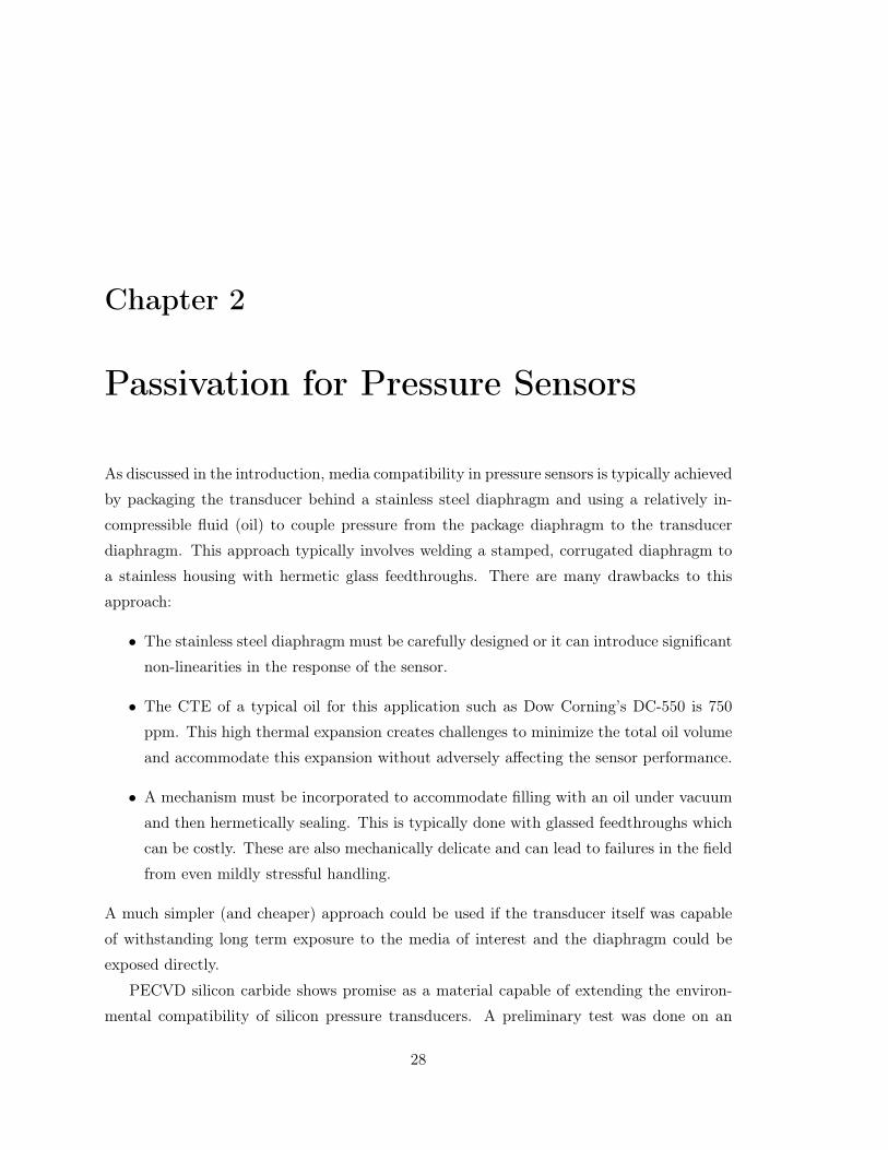
PECVD silicon carbide shows promise as a material capable of extending the environ-
mental compatibility of silicon pressure transducers. A preliminary test was done on an
28
29
NPC-103 pressure sensor from Lucas NovaSensor (Fremont, CA). The entire sensor, ce-
ramic substrate and bond wires were coated with approximately 300 nm of PECVD silicon
carbide carbide deposited using 1000mTorr, 1200 sccm 2% Si in Ar, 300 sccm CH4, a high
frequency power of 75W for 5 s, and a low frequency power of 150W for 10 s.
A discoloration around the periphery of the ceramic observed after the deposition indi-
cated the die attach material had experienced some level of oxidation or decomposition from
exposure to the high deposition temperature. A process for deposition on a fully packaged
part would require using a high temperature packaging material such as benzocyclobutene
(BCB).
Figure 2.1: Uncoated and coated pressure sensors after 45 minutes exposure to KOH.
The coated, packaged pressure sensor was then placed in 22% KOH at 80 °C along with
an uncoated sensor. After 45 min, the diaphragm of the uncoated sensor was completely
etched away. The coated sensor was still intact. Both are shown in Figure 2.1. Tests on
the coated pressure sensor showed that although stress in PECVD silicon carbide was low
enough so as not to induce offsets, the signal was significantly reduced, indicating that the
mechanical properties of the carbide films must be accounted for in sensor design.
Based on these promising results, a more detailed study was done on the characteristics
of PECVD silicon carbide that would specifically affect pressure sensor design. Mechanical
characterization, measurement of sensor performance, and analysis of corrosion resistance
was performed in collaboration with Thomas Kim, Bishnu Gogoi, Slobodan Petrovic, and
David Monk of the Motorola Sensor Products Division, and John Heck of the Berkeley
Sensors and Actuator Center.

30 CHAPTER 2. PASSIVATION FOR PRESSURE SENSORS
2.1 Optimization
In order to obtain an optimal set of deposition conditions specifically for a pressure sensor, a
two-level, four variable DOE was performed set up and samples were generated. Deposition
conditions for this DOE are listed in Table 2.1
Table 2.1: Deposition conditions for PECVD silicon carbide DOE
Deposition Parameters Set PointSilane Flowrate (sccm) 2840
Methane Flowrate (sccm) 1000, 1440, 1880Pressure (mtorr) 1600
High Frequency Power (W) 100High Frequency Cycle Time (s) 2.0, 4.5, 7.0
Low Frequency Power (W) 50, 100, 150Low Frequency Cycle Time (s) 2.0, 4.5, 7.0
Temperature (°C) 350
Due to equipment failure and availability, four points in the DOE were unable to be
completed. The list of samples and deposition conditions can be found in Table 2.2.
2.2 Mechanical Properties
2.2.1 Experimental Setup
The first step in assessing the effect of adding PECVD silicon carbide to a piezoresistive
diaphragm pressure sensor is to measure its mechanical properties. Establishing these pa-
rameters is important for use in analytical and finite element models used to predict sensor
performance. Young’s modulus and hardness were measured by nanoindentation using a
Nano Indenter II® mechanical properties microprobe (MPM) (MTS Nano Instruments,
Inc., Oak Ridge, TN). A Berkovich indenter was used to generate load-displacement curves
for two test samples. Samples for nanonindentation were prepared with thicknesses of 1 mm
and 2 mm using the centerpoint deposition condition. Wafers were sawn into one-inch squares
for testing. Poisson’s ration was assumed to be 0.25 following literature values recorded for
PECVD silicon carbide [30]. Khakani et al. have correlated hardness, Young’s modulus,
and Poisson’s ratio to the stoichiometric ratio of Si to C for α-SixC1-x:H with 0.4 < x <0.67.
The value of 0.25 for Poisson’s ratio was chosen as it represents the mean value at the upper

2.2. MECHANICAL PROPERTIES 31
Table 2.2: Conditions are listed below for a two-level, four-variable DOE of PECVD siliconcarbide deposition parameters. Missing cells are designated with a dash (-).
Wafer CH4Flowrate
(sccm)
hf Time(s)
lf Power(W)
lf Time(s)
- 1000 2 50 2B-08 1000 2 50 7B-01 1000 2 150 2A-17 1000 2 150 7A-23 1000 7 50 2B-06 1000 7 50 7B-04 1000 7 150 2- 1000 7 150 7
A-15 1880 2 50 2- 1880 2 50 7
A-05 1880 2 150 2- 1880 2 150 7- 1880 7 50 2- 1880 7 50 7- 1880 7 150 2
A-22 1880 7 150 7D-01 1440 4.5 100 4.5D-02 1440 4.5 100 4.5
end of x. To calculate Young’s modulus, the reduced modulus (Er) was employed, defined
as
S =2√πEr√A (2.1)
and
Er =
[1− ν2fEf
+1− ν2iEi
]−1
where Ei and νi are Young’s modulus and Poisson’s ration for the indenter, respectively,
and Ef and νf are Young’s modulus and Poisson’s ration for the thin film.
Because the stress in deposited thin films affect the electrical performance of piezore-
sistive transducers [73], this is an important property to measure over temperature. Films

32 CHAPTER 2. PASSIVATION FOR PRESSURE SENSORS
were deposited with different thicknesses on 4 inch diameter, n-type (100) blank wafers. The
resulting radius of curvature change was measured using a Tencor FLX-2320 (Tencor Instru-
ments, Milpitas, CA). As-deposited stress was calculated from the radius of curvature (R)
using Stoney’s equation:
σ =Est
2s
6 (1− νs)Rtf(2.2)
where Es/ (1− νs) is the biaxial modulus of the silicon substrate (1.805 x 10¹¹ Pa for <100>
silicon [74], ts is the thickness of the substrate, tf is the thickness of the deposited film, and
σ is the calculated film stress. Differences in the coefficients of thermal expansion (CTE)
between the film and substrate were calculated using the measurements from the Tencor
FLX-2320 system programmed with a selected temperature ramp. The temperature was
ramped from 20 ºC to 400 ºC over 60 minutes. Samples were cooled back down to 40 ºC over
150min using a nitrogen gas flow. Stress vs. temperature measurements were performed on
all available samples from the DOE table. The slope between 300 ºC and 40 ºC during the
ramp down period was used to calculate the CTE for carbide using:
Slope =dσ
dT=
Ef1− νf
∆α (2.3)
where Ef/ (1− νf ) is the biaxial modulus of the thin film and ∆α is the difference in CTE
between the silicon and the thin film. Multiple runs were performed on a centerpoint wafer
to determine both hysteresis and changes in dσdT .
Stiffness is derived from the initial slope of a load vs. displacement curve (assumed to
behave as a power law function) at the beginning of the unloading cycle. The equations of
relevance are:
P = αhm (2.4)
and
S =dP
dh
∣∣∣∣∣Pmax
dσ
dT(2.5)
where P is the load, h is the displacement, α is a constant, m is a constant assigned
according to the punch geometry [75], and S is stiffness. Hardness (H) is calculated by

2.2. MECHANICAL PROPERTIES 33
dividing the load by the area of contact (A) of the indenter on the film.
H =P
A(2.6)
2.2.2 Results
Nanoindentation measurements revealed that PECVD a-SiC:H undergoes both plastic and
elastic deformation as the indenter is loaded. Unexpected profiles with non-zero slopes were
observed in plots of both hardness and modulus of elasticity as a function of normalized
displacement. The abscissa value is the displacement of the indenter divided by the total
film thickness for the given sample; the x-value is the fraction of penetration by the indenter
on the total available film thickness. Each point on the graph represents the mean value of
several measurements. Error bars are plotted as ±1 standard deviation.
2.2.2.1 Young’s Modulus
Figure 2.2 shows a plot of Young’s modulus versus normalized displacement for two samples
deposited with 1 mm and 2 mm. The Young’s modulus profiles for the two samples are similar
with a slight increase in the y-direction for the sample with 2 mm of silicon carbide. The
surprising feature of the profiles is that there is a slope to the calculated Young’s modulus,
indicating that the film responds differently (albeit in a linear fashion) at different levels of
load indentations. Typically, the profiles would plateau after about 10% of the test film has
been penetrated. The plateau observed for the 1 mm sample near the end of the normalized
displacement from 0.9 to 1 is more a feature of the silicon substrate than the silicon carbide
film. It appears that is that the silicon substrate, which has a higher value of Young’s
modulus (~160GPa) is confounding the expected non-zero slope of the silicon carbide film
profile. To obtain a good value of the Young’s modulus for the carbide itself, the results are
extrapolated to the zero displacement point at the y-intercept.
2.2.2.2 Hardness
Figure 2.3 shows a plot of hardness versus normalized displacement for two samples deposited
with 1 mm and 2 mm. As with the Young’s modulus, the hardness (H) also increases as the
film is being penetrated and the hardness must be determined by extrapolating to the zero
displacement point at the y-intercept.
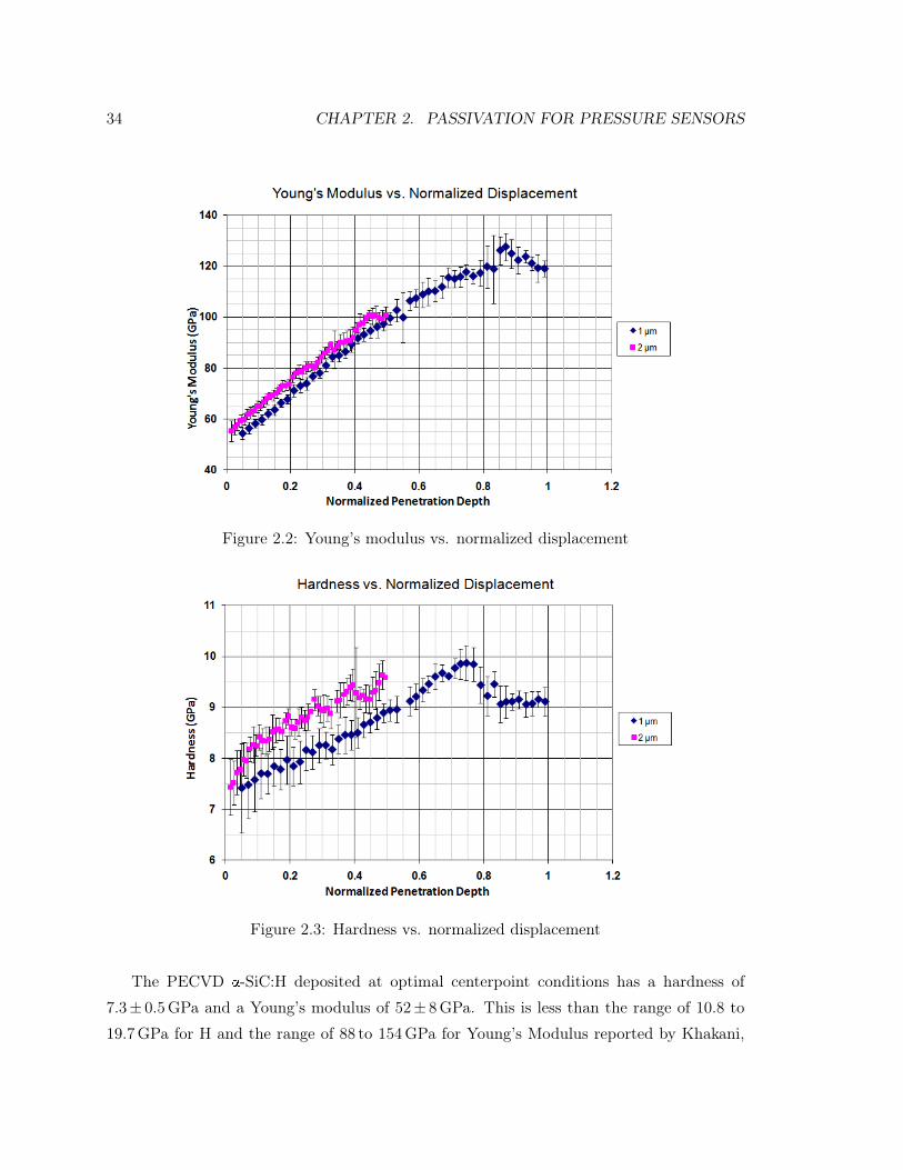
34 CHAPTER 2. PASSIVATION FOR PRESSURE SENSORS
Figure 2.2: Young’s modulus vs. normalized displacement
Figure 2.3: Hardness vs. normalized displacement
The PECVD a-SiC:H deposited at optimal centerpoint conditions has a hardness of
7.3± 0.5GPa and a Young’s modulus of 52± 8GPa. This is less than the range of 10.8 to
19.7GPa for H and the range of 88 to 154GPa for Young’s Modulus reported by Khakani,

2.2. MECHANICAL PROPERTIES 35
et. [30], indicating that the film is silicon-rich PECVD a-Six C1-x:H film with x > 0.67. This
is consistent with the FTIR results discussed in chapter 1.
2.2.2.3 Stress
The stress of deposited films for centerpoint deposition conditions on blank wafers is shown
in Figure 2.4. For films deposited at 400 nm, the stress ranged from -47 to -9MPa. While
the term “low stress” is somewhat subjective, lower than 50MPa in absolute stress value
is generally considered acceptable, particularly in the context of this application. Room
temperature stress measurements were also made on samples of 0.8, 1.0, and 1.2 mm. Results
show that the stress of PECVD silicon carbide shifts more tensile as the film thickness
increases and approaches 10MPa almost asymptotically.
Figure 2.4: Room temperature stress vs. thickness of deposited films
2.2.2.4 Stress and CTE
Stress, CTE, and dσdT values are recorded in Table 2.3. Recall that dσ
dT is the slope from
the linear portions taken from 300 °C to 40 °C during the ramp down cycle of stress vs.
temperature plots. Since not all of the DOE cells were fulfilled, a complete screening analysis
could not be run. Analyzing the data that was available showed no first order interactions

36 CHAPTER 2. PASSIVATION FOR PRESSURE SENSORS
of the four deposition variables (to 95% confidence levels) to either the stress or CTE values
for PECVD a-SiC:H. There was no unique set of coefficients to form a linear combination.
Due to the lack of degrees of freedom, second order parameters were also biased and no
higher order model could be generated. However, it seems apparent from comparing the
changes of the output levels for repeated runs with variations in only one of the four input
variables that each deposition condition was highly significant for room temperature stress
values (20°C) but not so significant for CTE values. Centerpoint PECVD a-SiC:H films
had a CTE value of 2.5 ppm/°C at 25 °C and 3.1 ppm/°C at 125 °C. CTE values of 2.4 and
3.0 ppm/°C at 25 and 125°C respectively were used for the silicon substrate. It is interesting
to note that PECVD a-SiC:H has a higher coefficient of thermal expansion than silicon,
since most passivation films have lower CTE values. This material property is significant
in analyzing devices with silicon carbide where the performance metric value is based on
temperature.
Table 2.3: Mechanical properties of trials in DOE
Wafer CH4Flowrate
(sccm)
hfTime(s)
lfPower(W)
lfTime(s)
Stress20 ºC(MPa)
dσdT
(MPa/ºCCTE25 ºC
(ppm/ºC
CTE125 ºC
(ppm/ºC)- 1000 2 50 2 - - - -
B-08 1000 2 50 7 -28.5 -0.116 2.5 3.1B-01 1000 2 150 2 83.2 -0.365 2.8 3.4A-17 1000 2 150 7 -8.1 -0.122 2.5 3.1A-23 1000 7 50 2 -102.5 -0.256 2.7 3.3B-06 1000 7 50 7 119.5 -0.442 2.8 3.4B-04 1000 7 150 2 -12.8 -0.111 2.5 3.1- 1000 7 150 7 - - - -
A-15 1880 2 50 2 -19.0 -0.114 2.5 3.1- 1880 2 50 7 - - - -
A-05 1880 2 150 2 -44.3 -0.149 2.5 3.1- 1880 2 150 7 - - - -- 1880 7 50 2 - - - -- 1880 7 50 7 - - - -- 1880 7 150 2 - - - -
A-22 1880 7 150 7 -32.7D-01 1440 4.5 100 4.5 -42.7D-02 1440 4.5 100 4.5 -46.2
Stress versus temperature profiles were strikingly similar for the DOE points investigated,

2.2. MECHANICAL PROPERTIES 37
including the centerpoint. The hot temperature excursion consistently decreased the stress
value by 11± 5MPa at T=40 °C, making the films more tensile. Wafers from run A-23,
which had a room temperature stress of -103MPa, showed greater stress hysteresis with a
delta value of 60 MPa Wafer B-06, which had a room temperature stress value of 120MPa,
showed little hysteresis. Annealing occurs beyond the deposition temperature of 350 °C and
the stress versus temperature lines criss-cross randomly between 325 °C and 400 °C. Figure
2.5 illustrates multiple hot temperature excursions on a centerpoint test wafer deposited with
400 nm PECVD α-SiC:H. With each consecutive run, the stress value decreases. Annealing
still occurred after four runs but the stress hysteresis was lessened after each temperature
cycle. The initial change of stress was 11MPa. On run four, the delta was 4MPa at
T=40 °C. The slope of stress change, dσdT , remained consistent over multiple runs. This
demonstrates that the residual stress from a PECVD silicon carbide layer can be affected by
an anneal cycle. The sensitivity and offset of a pressure sensor would be affected by adding a
protective layer. Having the ability to minimize this impact by reducing the intrinsic stress
is an attractive quality of PECVD α-SiC:H. Because the anneal temperature is metal and
CMOS compatible, it can be easily incorporated into a production flow at minimal cost and
complication.
Figure 2.5: Stress vs. temperature

38 CHAPTER 2. PASSIVATION FOR PRESSURE SENSORS
2.3 Effect on Pressure Sensors
The addition of a thin film to a piezoresistive pressure sensor affects the stiffness and stress
of the diaphragm, which in turn influences parametric behavior. A series of experiments
were conducted where various thicknesses of carbide were deposited on a low range (0 to 6
kPa) pressure sensor. Studying the variations of sensitivity and offset with thickness were
used to correlate the mechanical properties of the film with their effect on the behavior of
the sensor. The PECVD α-SiC:H was deposited onto the die as the last film in a series
of passivations. The passivation-film stack makes up about 5 % of the total diaphragm
thickness (18 mm).
2.3.1 Initial Offset
The offset induced by stresses in the encapsulating film are shown in Figure 2.6. As carbide
thickness increases, offset increases, suggesting that PECVD silicon carbide is tensile at
higher film thickness. This agrees with the material analysis of the stress levels as a function
of film thickness, as shown in Figure 2.4. A thickness of 400 nm of carbide shifted the initial
offset positive by approximately 1.5mV/V. The 800 nm showed the same rate of effect per
thickness, shifting the initial offset voltage positively by roughly 3.0mV/V.
Figure 2.6: Initial offset

2.3. EFFECT ON PRESSURE SENSORS 39
2.3.2 Sensitivity
As expected, the sensitivity decreased as thicker layers were deposited. The loss in sensitivity
indicates that the stiffness of the diaphragm increased due to the compressive stress applied
by the carbide film and the increase in passivation film thickness. During the material
characterization of carbide, compressive stress was observed for the 400 nm thickness, but
not the 800 nm thickness. Although carbide was seen to be tensile for films thicker than 800
nm, higher thickness of the film may decrease the sensitivity.
Figure 2.7: Sensitivity vs. thickness of deposited film
2.3.3 Temperature Coefficient of Sensitivity (TCS)
An important result is the decrease in magnitude of the temperature coefficient of sensitivity
(TCS) with the addition of PECVD silicon carbide. The TCS vs. film thickness is shown in
Figure 2.8. Typically the addition of an LPCVD silicon dioxide or PECVD silicon nitride
film on the pressure sensor diaphragm increases the magnitude of TCS, making the device’s
performance in sensitivity more temperature dependent. Differences in the CTE values for
these films may explain the variable effect on TCS; specifically, silicon oxide and PECVD
silicon nitride have CTE values less than silicon, whereas PECVD silicon carbide had a
CTE value greater than silicon. Additionally, correlations between TCS and sensitivity for

40 CHAPTER 2. PASSIVATION FOR PRESSURE SENSORS
devices with variable thicknesses of silicon dioxide have shown that an increase in oxide film
thickness increases the magnitude of TCS. The opposite is observed with the addition of
PECVD silicon carbide. At a given sensitivity, the magnitude of TCS decreases, reducing
the level of electronic trimming required.
Figure 2.8: TCS vs. film thickness
Figure 2.9: The correlation of TCS with sensitivity for two thicknesses of PECVD SiC

2.4. CORROSION RESISTANCE 41
2.4 Corrosion Resistance
Several mechanisms can cause the breakdown of a protective coating. The etchant can attack
the film directly and remove it. A second mechanism is through defects. These defects can
be present in the film as deposited due to particles in the system. In some cases, nodules or
nucleation sites can form as a natural part of the deposition process and become points that
are not technically defects, but which are chemically different from the intended film and
susceptible to chemical attack. Defects can also be created by scratching during handling.
Defects allow the etching chemistry to reach the substrate and undercut the protective film.
The third mechanism is a function of the diffusive permeability of the film. If the film is
permeable to the etchant, or even to potentially corrosive gases in the environment such as
oxygen, long term exposure will lead to failure.
2.4.1 Etch Resistance
The etch resistance of the specific films in this study was measured using the same technique
as discussed in chapter 1. The change in thickness was measured over time using ellipsometry.
Two blank silicon wafers were coated with 400 nm of the carbide using the centerpoint set
of parameters in Table 2.1. For comparison, two separate PECVD silicon nitride films were
tested on two wafers each. This etch resistance test was done with 23wt.% KOH at 95 °C
using a fixture for single-sided wafer etching to prevent excessive overetching of the wafer
backside.
The etch depth results are shown in Figure 2.10. All the nitrides etched at a similar
etch rate, 5.29± 0.49 nm/min. The carbides etched at 0.79± 0.08 nm/min. This measurable
etch rate is different than what was in measured for 33wt.% KOH at 80 °C, which showed
no etch rate above 0.05 nm/min. The difference in etch rates between this experiment and
the previous one shows that bulk etching may be a mechanism of failure for long-term
exposure in extreme chemistries. Evaluation of the suitability of PECVD silicon carbide
for a particular application must be done on a case-by-case basis, tailoring the qualification
tests for specific conditions.
2.4.2 Linear Polarization
Linear polarization or linear sweep voltammetry can be used to investigate the diffusive per-
meability of the film [76]. Test substrates were prepared by patterning aluminum electrode

42 CHAPTER 2. PASSIVATION FOR PRESSURE SENSORS
Figure 2.10: Etch rates of PECVD silicon carbide and PECVD silicon nitride
arrays on a thermally oxidized wafer. PECVD silicon carbide was deposited to a thickness
of 400 nm using the centerpoint recipe from table 2.1. A test substrate was also prepared
using 300 nm of PECVD silicon nitride for comparison.
Figure 2.11: Cross-section of die for electrochemical studies
The wafers were then patterned and etched to expose the bond pads. Wafers were diced
and packaged into a 6-pin unibody package. A chemically resistant epoxy was used to protect

2.4. CORROSION RESISTANCE 43
the bond pads, bond wires, and edges of the die from corrosion while exposing the coated
electrode. The experimental setup is shown in Figure 2.12. A platinum wire was used as
the counter electrode. A Ag/AgCl reference electrode was used. The coated die was the
working electrode as the device under test (DUT).
Figure 2.12: Fixture for electrochemical corrosion studies
The prepared devices were immersed in 23wt% KOH at room temperature for 48 h with
measurements taken at 0, 24, and 48 h. The corrosion of the underlying aluminum was
expected to proceed via an oxidation (Al→Al+3+ 3e-). The leakage current through the
film was measured by applying a positive potential, ramped at 100mV/s from 0 to 5V
As can be seen from the results at 48 h, the PECVD silicon carbide had negligible leakage
currents and no signs of permeability under the conditions tested. The PECVD silicon
nitride film tested had a linear, resistive current profile indicating diffusion through the
membrane. Some nitride films have been tested and shown results similar to the carbide [77].
The permeability of this particular PECVD silicon nitride is more a function of the deposition
conditions than the chemistry of the film. Exact determination of the resistance of the
carbide sample was not possible because the current at 5V was still below the noise floor
of the potentiostat. The resistance of the sample was greater than 200MW. The equivalent
resistance of the nitride sample was 220 kW.

44 CHAPTER 2. PASSIVATION FOR PRESSURE SENSORS
Figure 2.13: Linear polarization plot of PECVD silicon carbide and a failing sample ofPECVD silicon nitride for comparison.
2.4.3 Electrochemical Impedance Spectroscopy
One drawback to linear polarization is that the absolute value of the current measurements
are dependent on surface area. Electrochemical Impedance Spectroscopy (EIS) has long
been established as a more sophisticated approach to analyzing corrosion behavior. Complex
equivalent circuit models are replete throughout the literature [78–81]. The DC potential
across the film was set at 0V and 5mV sine wave was swept between 0.1 Hz and 1 MHz.
The results are shown in Figure 2.14.
The resistance and capacitance vary inversely relative to each other with respect to both
area and thickness. The cutoff frequency of the dominant pole, f c, can be used as a figure
of merit to compare the quality of different films, taking care to account for any changes in
dielectric constant. The cutoff frequency of the failing sample, Sample 2, is approximately
600Hz. The apparent resistance between 1Hz and 1 kHz is 6MW with a capacitance of
47 pF. Sample 1 does not show a cutoff frequency in the range examined, indicating that
the resistance of this sample is greater than 5GW. The fact that one sample did not fail and
another did is a strong indication that the failure mechanism results from a defect, either

2.5. SUMMARY 45
Figure 2.14: EIS of two PECVD silicon carbide samples after 48 hours. Sample 2 showscorrosion behavior.
due to processing or due to handling. It is not an intrinsic property of the film.
2.5 Summary
Preliminary results using PECVD silicon carbide to protect silicon diaphragm pressure sen-
sors were promising. The mechanical properties that would be significant for the design of
a diaphragm pressure sensor were determined through direct characterization. The results
showed that carbide could be incorporated into a design with minimal effort. This was con-
firmed by depositing the carbide as a passivation layer to an existing pressure sensor design.
Measurements of the impact it had on the performance were consistent with the expected
effects from the mechanical properties measured. PECVD silicon carbide was compatible
with, and in some respects was beneficial to a diaphragm pressure sensor.
Accelerated corrosion studies showed that while the carbide protected the silicon di-
aphragm sufficiently, it was not successful when applied to existing packaging and bond
wires. Additionally, results showed that some failures are a result of fabrication defects and
not a failure of the inherent film. The mixed results gives an indication of promising avenues

46 CHAPTER 2. PASSIVATION FOR PRESSURE SENSORS
for future work. One would be to improve the compatibility of bond wires and packaging
with the deposition process, particularly the deposition temperature of 350 °C. Both the
deterioration of the package and the adhesion to the bond wires are concerns. Second, the
deposition system requires optimization, specifically for PECVD silicon carbide, to reduce
the level of particles and point defects so that reliable thin films can be deposited at a
reasonable thickness.

Chapter 3
An Iridium Microelectrode Array
Introduction
Microelectrodes have been fabricated since the early days of micromachining. They have
been used in a variety of applications ranging from extracellular recording of electrical poten-
tials in live tissues to analytical chemistry. By using such inert materials as PECVD silicon
carbide and iridium in the fabrication of a microelectrode array, it is possible to fabricate
a chemical transducer that can withstand continual exposure to such media as hydrofluoric
acid (HF).
The work presented in this chapter includes improved methods for deposition and pat-
terning of iridium for micromachining applications, the application of PECVD silicon carbide
as a chemically resistant coating of a microelectrode array, and the demonstration of its use
in hydrofluoric acid.
The analysis of the microelectrode array in HF was done in collaboration with Dr. Stan
Tsie of ChemTrace Corporation, Hayward, CA. The original design of the array and was
done by Chris Storment, Stanford University, Stanford, CA.
3.1 Background
Microelectrodes have a number of characteristics that result in improved performance over
their macroscopic counterparts for many applications. A brief overview is presented here,
but a detailed discussion can be found in Analytical Electrochemistry by Joseph Wang [82].
Advantages offered by microelectrodes include:
47

48 CHAPTER 3. AN IRIDIUM MICROELECTRODE ARRAY
• localized measurements (an advantage in such endeavors as cellular recording),
• reduced resistive drop (allows measurements in low conductivity environments),
• reduced capacitance (faster time constants), and
• enhanced mass transport (enhanced signal-to-noise ratios).
The last property is of particular interest to this work as it leads to the improved performance
of microelectrodes for heavy metal analysis using square wave anodic stripping voltammetry
SWASV, discussed below.
3.1.1 Diffusion Behavior
One of the main advantages of a microelectrode is the nature of its diffusion profile. Standard
planar electrodes establish a planar diffusion profile. Hemispheric electrodes establish a
hemispheric diffusion profile, which has a planar and a radial component. It is the radial
component of the diffusion profile that leads to improved mass transport for a given electrode
area. Conditions for hemispheric diffusion are that
r0 √D0t (3.1)
where D0 is the diffusion layer thickness, t is the electrolysis time, and r0 is the smallest
dimension of the electrode. This effect has been shown to begin in electrodes with radii
as large as 300 mm [83]. The working electrode for the SWASV studies done here was
approximately 10 mm, well into the regime where this effect is established. Experimental
data have shown that this hemispheric profile is established on the order of 1 s [84].
The time necessary to reach steady state, spherical behavior is important, as it sets a
lower limit on deposition time or the preconcentration time for stripping techniques, and an
upper limit on the frequency of analysis. Theoretical calculations [85,86]
tε =d2
π3Dε2(3.2)
where tε is the time, d is the disk diameter in meters, D is the diffusion coefficient, and ε
is the percentage of final value obtained by time tε. For a typical diffusion constant of 1 x
10-9 m2/s, the current reaches 95% of the steady state value by 1.3 s.

3.1. BACKGROUND 49
3.1.2 Square Wave Anodic Stripping Voltammetry
SWASV analysis of heavy metal ion concentration was chosen to demonstrate the use of the
microelectrode array in caustic media. Previous work had demonstrated this application in
more conventional electrolytes such as perchloric acid and glacial acetic acid [87–89].
In the first step, a mercury hemisphere was plated onto the surface of the iridium elec-
trode. The choice of iridium as the electrode material was critical to the success of the
plating. Deposition on glassy carbon electrodes has poor reproducibility and adhesion is un-
reliable. With other metal electrodes such as platinum, mercury tends to form intermetallic
compounds (alloy) that leads to the dissolution and failure of the electrode. Iridium does
not suffer from either of these limitations [89].
Once the mercury had been plated, the electrode was then transferred to the solution
to be analyzed. SWASV is a two phase process. The first phase is called the preconcen-
tration phase. During this phase, the electrode is biased cathodically (negatively) relative
to solution. The mercury electrode can be considered equipotential. Cations of interest are
reduced at the surface of the mercury hemisphere. In their reduced or neutral state, the
metals of interest are much more soluble in the mercury than in the aqueous solution and
they concentrate within the electrode.
Figure 3.1: Steps in square wave anodic stripping voltammetry
The ratio of oxidized to reduced species is derived from the Nernst equation [90]:
E = Eφ +RT
nFln
(CνiOi
CνiRi
)(3.3)
where
E is the half-cell reduction potential,
Eφ is the standard half-cell potential,
R is the Universal Gas constant = 8.314 J/mol·K.

50 CHAPTER 3. AN IRIDIUM MICROELECTRODE ARRAY
T is the absolute temperature,
F is the Faraday constant = 9.648 x 10⁴ C/mol,
n is the number of electrons transferred in the reaction, and
CνiRi, CνiOi
are the concentrations of the reduced and oxidized species respectively.
The Nernst equation states that the electrochemical potential of an oxidized species
in equilibrium with its reduced species is proportional to the logarithm of their relative
concentrations. Inversely, the relative concentration of the species is dependent upon the
applied potential in a quasi-equilibrium (steady state) situation. For a given potential, at
the mercury interface, the relative concentrations of the different species can be determined
from
CνiRi
CνiOi
= enFRT (E
0−E). (3.4)
The concentration of the reduced metal species decreases exponentially as the electrode
potential moves beyond the standard half-cell potential. The floor on the preconcentration
voltage in an aqueous environment is approximately -1.2V relative to a Ag/AgCl reference
electrode. Below this potential the hydrolysis of water begins to compete and interfere with
the preconcentration reaction. As can be seen from the graph in Figure 3.2, the concentration
of the oxidized species at the interface can be considered to be zero even for species with
redox potentials as low as -1.1 V
As the concentration of reduced species at the interface decreases, a flux of metal atoms
from the center of the electrode to the surface is established. This progresses according to
Ficks first law, adjusted for spherical diffusion.
δC (r, t)
δt= D
δ2C (r, t)
δr2+
2
r
δC (r, t)
δr(3.5)
The longer the preconcentration time, the higher the concentration of the analyte in the
mercury hemisphere and the more sensitive the analysis. Preconcentration times from 100 s
to 15minutes are typical. Essentially all of the metal ion flux to the surface is a result of
steady state diffusion that is linearly dependent upon the concentration differential. Thus
the amount of analyte dissolved in the mercury hemisphere is linearly dependent on both
the concentration in solution and the preconcentration time.
The second phase is called the stripping phase. In the stripping phase, the voltage is
stepped anodically (positive relative to solution) using a staircase wave. Current is sampled

3.2. FABRICATION 51
Figure 3.2: Ratio of oxidized to reduced species vs. electrode potential
at the end of both the forward and reverse phase of the wave and subtracted (Figure 3.3).
By doing this, the Faradic current due to the metal oxidation can be separated from the
capacitive charging current of the electrode.
3.2 Fabrication
3.2.1 Overview
A diagrammatic cross section of the microelectrode array is shown in Figure 3.4. An overview
of the fabrication process is as follows. The starting material is a 4-inch (100) silicon wafer.
A layer of wet thermal oxide is first grown to a thickness of 500 nm and then patterned using
an oxide plasma etch (Applied Materials AMT 8100 Hexagonal Etching System, Applied
Materials, Inc., Santa Clara, CA). This provides a high quality underlying dielectric, reliable
alignment marks for later in the process, and a recess area surrounding the chip so that no
oxide is exposed along the edges after dicing.
The electrode layer is then deposited. A 25 nm tacking layer of chromium followed by a
350 nm layer of iridium are evaporated using an Innotec ES26C e-beam evaporator (Innotec

52 CHAPTER 3. AN IRIDIUM MICROELECTRODE ARRAY
Figure 3.3: Stripping phase of SWASV
Figure 3.4: Diagrammatic cross-section of the microelectrode array
Group, Inc., Simi Valley, CA) and patterned into the electrode arrays using a germanium-
aluminum liftoff technique discussed in detail in section 3.2.2.3. Liftoff is accomplished with
4:1 sulfuric peroxide mixture.
The interconnect and bond pad layer is then deposited and patterned using the Shipley
liftoff layer (LOL) technique (Shipley Company, Marlborough, MA). This is a two-layer
technique whereby Shipley LOL is spun on, followed by Shipley 3612 photoresist. Both
layers are patterned in the same photolithography step. A 25 nm tacking layer of chromium
followed by a 500 nm layer of gold is evaporated and lifted off using acetone, followed by
isopropyl alcohol, and finally a 4:1 sulfuric peroxide mixture to clean the surface.
A 1 mm layer of PECVD silicon carbide is then deposited as the encapsulating layer.

3.2. FABRICATION 53
Openings to the electrodes and the bond pads are patterned using an SF6 plasma etch.
Details of carbide deposition and etching are discussed in Chapter 1.
3.2.2 Stress Control of Iridium
The initial electrodes were fabricated by sputter depositing 300 nm of iridium on top of a
25 nm chromium tacking layer. Because iridium is relatively inert, it is difficult to pattern
directly. A liftoff technique was required.
Figure 3.5: SEM of a failed iridium microelec-trode pad
One hindrance to repeatable production
of thin-film iridium electrodes is the stress
that is typical in both sputtered and evapo-
rated films of iridium. Stresses on the order
of a several GPa have been observed. In
early runs of the arrays, stress often caused
tearing of the electrodes as shown in Fig-
ure 3.5. Three methods were utilized to
overcome this limitation. The first was the
use of ion bombardment during evapora-
tion to reduce the tensile stress of the film.
The second was the use of a staggered de-
position process, in which cooling periods
were inserted between short deposition cy-
cles to reduce the stress from CTE mis-
match. The third was the development of
a stress-tolerant set of liftoff layers. Stress
was measured by wafer curvature using an SMSI 3800 stress gauge (Scientific Measurement
Systems, Inc., San Jose, CA).
3.2.2.1 Ion-assisted Deposition
Ion-assisted physical vapor deposition (IAPVD) has been used to help control stress, stoi-
chiometry, morphology, and tribological behavior of many different films. Some examples
from the literature include diamond-like carbon (DLC) [91], cubic boron nitride (c-BN) [92],
and silver [93]. The earliest reference of its specific use in this way is Mattox [94]. In
1994, Greer reported its use to control the stress of molybdenum thin films for use in flat

54 CHAPTER 3. AN IRIDIUM MICROELECTRODE ARRAY
panel displays [95]. In IAPVD, a stream of inert ions is directed at the surface of the wafer
during thin-film deposition. The ions have enough kinetic energy to promote surface re-
arrangement, though not enough to sputter-etch the surface. It should be noted that this
technique is distinct from one in which the incident ions react chemically with the thin-film
material.
For the iridium deposition, a Mark I gridless ion source (Commonwealth Scientific Cor-
poration, Alexandria, VA) was used to generate a stream of argon ions. The stream of ions
was directed to cover a section of the planetary that was rotated during deposition. The
energy of the ion atoms was approximately 100 eV, which was too low to cause sputtering.
The ion current density based on the specified performance of the ion gun and distance from
the wafers was approximately 0.05mA/cm2. The deposition rate was kept low at 0.1 nm/s
to maximize the effect of the ion bombardment.
3.2.2.2 Staggered Deposition
The coefficient of thermal expansion (CTE) for the materials used in the electrode process
are listed in Table 3.1. Because the CTE for the metals are all larger than that of silicon, it
is clear that if the silicon wafer is heated during deposition, the thin film will become more
tensile as the wafer cools. Unfortunately, evaporation is problematic on two fronts. Thin
films are almost always tensile, and the energy directed at the crucible during evaporation
radiates outward and heats the wafers. Consequently the CTE mismatch acerbates, rather
than ameliorates the stress problem.
Non-reversible temperature labels from Omega (Omega Engineering, Stamford, CT)
were used on the backs of wafers during trial runs. Temperatures in excess of 180 °C were
observed during typical continuous depositions of a full thickness of iridium.
Table 3.1: Coefficients of thermal expansion
Element CTEIridium 6.4Gold 14.2
Chromium 4.9Silicon 2.6
To help decrease the temperature at which the metal is deposited, iridium was deposited
in short bursts interspaced with long cooling periods. For each deposition, the temperature

3.2. FABRICATION 55
was monitored and deposition stopped as soon as the temperature in the chamber reached
80 °C. The wafers were allowed to cool approximately 1 h before resuming depositions, to
roughly 35 °C. At 0.1 nm/sec., it was usually possible to deposit 15-20 nm per period.
Table 3.2 shows the stress reduction achieved from three separate trial runs. For the trial
runs, 25 nm of chromium were deposited as a tacking layer, followed by 120 nm of iridium.
Table 3.2: Progressive reduction of stress in evaporated iridium
Type of Trial Stress (MPa)Standard Evaporation 2500Evaporation with Ion Gun Assist 1630Evaporation with Ion Gun Assist and StaggeredDeposition
360
It is acknowledged that a staggered deposition is not a practical solution to high-stress
films. Achieving even a reasonable thickness film could take days. What the experiment
did illustrate successfully though was the significant improvement that controlling wafer
temperature can have on the stress of deposited films. It supports the case for the addition
of active wafer cooling, or, in some cases maybe heating, to a deposition system where stress
control is important.
3.2.2.3 High-Stress Liftoff Layers
Given the limitations of the accessible deposition systems, the steps taken above were suc-
cessful in reducing, but could not eliminate the measured stress. It was observed that
although the iridium itself could withstand stresses on the order of several hundreds of
MPa, the underlying photoresist-aluminum bilayer could not. Often during deposition, the
underlying photoresist layer would buckle and crinkle. This had the effect of generating par-
ticles during the deposition that would incorporate into the film and were suspected sources
of point defects.
Several material pairs were evaluated as alternate choices for a more stress-tolerant set
of liftoff layers. The materials had to satisfy several criteria.
• Suitable etch methods had to exist such that each layer could be patterned indepen-
dently in order to create the required liftoff undercut.
• These etch methods must be compatible with standard photoresist.

56 CHAPTER 3. AN IRIDIUM MICROELECTRODE ARRAY
• A liftoff chemistry had to exist that did not attack silicon dioxide, chromium, or
iridium. Preferably the liftoff would proceed with both layers to reduce the time
required.
• The layers had to accommodate a high stress iridium deposition without severe defor-
mation (buckling, cracking, or peeling).
After several experiments with a series of possible layers, including aluminum-low-temperature
oxide (LTO), LTO-aluminum, and aluminum-silicon (sputtered), the best performance was
obtained with an aluminum-germanium bilayer.
• Aluminum can be patterned in aluminum etch. Germanium also etches in aluminum
etch, though at a much slower rate. The liftoff undercut can then be created with a
very low power SF6 plasma etch, which does not attack aluminum.
• Germanium etches very rapidly in an SF6. It etches so quickly, in fact, that it was
necessary to drop the power below 1.6W/cm2 to achieve a controllable, repeatable
undercut etch. Undercut etches were completed in 80 s. At this power and for this
duration, no significant attack of the underlying silicon dioxide was observed.
• Aluminum and germanium both etch rapidly in sulfuric peroxide. This is an ideal
liftoff etch as the cavitation from oxygen evolution aids in the process, and sulfuric
peroxide does not attack chromium or iridium.
• The Al-Ge bilayer was able to withstand 400MPa of stress from a 350 nm deposition
of iridium without failure.
Results of the Al-Ge bilayer are shown in Figure 3.6. The SEM shows ideal dimensional
control of the undercut. The ability to deposit thicker layers of either material ensures
that no “dog-ears” or “stringers” from inadequate separation of the deposited layer does not
occur.
3.3 Electrode Design
While microelectrodes typically have superior performance relative to their macroscopic
counterparts, the signals themselves are small enough that they can be lost in the parasitics

3.3. ELECTRODE DESIGN 57
Figure 3.6: SEM cross-section of an aluminum-germanium liftoff bilayer after deposition ofiridium
of the electrochemical system. By making a microelectrode array, the signals at each elec-
trode are added together, achieving both the superior performance of a microlectrode with
an adequate signal-to-noise ratio for the electronic system. The electrode design used in the
evaluation of PECVD silicon carbide was an adaptation of a second generation microelec-
trode array design done by Chris Storment of Stanford University.
3.3.1 Working Electrode
The balancing considerations in sizing the working electrode were that it be small enough
to exhibit hemispheric diffusion profile behavior, large enough to fabricate repeatably and
robustly, and spaced far enough apart that diffusion spheres from each electrode did not
overlap.
Once reaching steady state, the diffusion thickness can be calculated from
δss =2πr2nFD0C
∗0
iL(3.6)
where
r is the radius of the electrode,
D0 is the diffusion constant of the species,
C∗0 is the bulk concentration of the oxidized species in solution, and
58 CHAPTER 3. AN IRIDIUM MICROELECTRODE ARRAY
iL is the limiting current for the electrode.
For a microelectrode, the limiting current of the electrode is
iL = 2πrnFD0C∗0 . (3.7)
Substituting and simplifying,
δss = r. (3.8)
.
The diffusion thickness is equivalent to the radius of the hemispheric electrode under
steady state [82] [96]. In a previous design, it was demonstrated by chronocoulometry
that for all time scales of interest, there was no significant overlap of diffusion spheres for
electrodes spaced 300 mm apart. In the design explored here, working electrodes were spaced
400 mm apart [84].
3.3.2 Reference Electrode
When it becomes necessary to establish a precise, absolute voltage within an electrochemical
cell, a reference electrode is used. With a reference electrode, the junction potential between
the electrode and the solution is stabilized to a known value by keeping the reference elec-
trode immersed in a solution of known concentration (typically saturated). This provides
an electrochemical “ground” into the solution. A diagram of a saturated calomel reference
electrode is shown in Figure 3.7.
Electrical contact is made to the test solution by bringing the reference and test solu-
tions into contact with each other across a glass frit. This is typical of reference electrode
configurations. A more thorough discussion of reference electrodes can be found in Brett
and Oliveira Brett [97].
The true reference electrode in microelectrochemistry is still a technical challenge. It
is often impractical to maintain a separate chemical environment within the microfluidic
system. Additionally, because electrical contact to the analyte is often made by bringing
the two solutions (test and reference) together across a glass frit, contamination of the test
solution is a problem. This is more of a problem on a microscale where small amounts of
contaminants can have a large impact on concentrations.
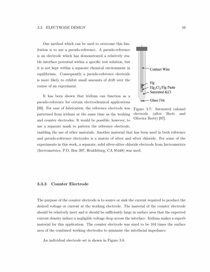
3.3. ELECTRODE DESIGN 59
Figure 3.7: Saturated calomelelectrode (after Brett andOliveira Brett) [97].
One method which can be used to overcome this lim-
itation is to use a pseudo-reference. A pseudo-reference
is an electrode which has demonstrated a relatively sta-
ble interface potential within a specific test solution, but
it is not kept within a separate chemical environment in
equilibrium. Consequently a pseudo-reference electrode
is more likely to exhibit small amounts of drift over the
course of an experiment.
It has been shown that iridium can function as a
pseudo-reference for certain electrochemical applications
[98]. For ease of fabrication, the reference electrode was
patterned from iridium at the same time as the working
and counter electrodes. It would be possible, however, to
use a separate mask to pattern the reference electrode,
enabling the use of other materials. Another material that has been used in both reference
and pseudo-reference electrodes is a matrix of silver and silver chloride. For some of the
experiments in this work, a separate, solid silver-silver chloride electrode from Invivometrics
(Invivometrics, P.O. Box 397, Healdsburg, CA 95448) was used.
3.3.3 Counter Electrode
The purpose of the counter electrode is to source or sink the current required to produce the
desired voltage or current at the working electrode. The material of the counter electrode
should be relatively inert and it should be sufficiently large in surface area that the expected
current density induce a negligible voltage drop across the interface. Iridium makes a superb
material for this application. The counter electrode was sized to be 104 times the surface
area of the combined working electrodes to minimize the interfacial impedance.
An individual electrode set is shown in Figure 3.8.

60 CHAPTER 3. AN IRIDIUM MICROELECTRODE ARRAY
Figure 3.8: Microelectrode array
3.4 Experimentation
3.4.1 Optimization of Plating Procedures
Before beginning further experimentation, a procedure was developed to improve the robust-
ness and repeatability of the mercury plating process. The reliability of SWASV depends
foremost on the quality of the Hg hemispheres plated on the probe. With the criteria of
this procedure, a poorly plated microelectrode array will be detected and re-plated before
it leaves the plating solution.
Unless otherwise noted, all analyses were carried out in a 0.1 M solution of perchloric
acid. Dilutions of standards for inductively coupled mass spectroscopy (ICPMS) were added
to the perchloric acid to achieve the desired concentrations of the analytes in question (SPEX
Industries, Edison, NJ). SWASV scans were run at 60Hz, from -0.1V to -1.2V relative to a
solid Ag/AgCl pseudo-reference electrode from Invivometrics. The step height was 25mV,
the step increment was 5mV.
In the optimized Hg plating procedure, the microelectrode array is cleaned by dipping
the tip in concentrated nitric acid for 5min. The tip is then rinsed thoroughly in deionized
(DI) water. To achieve reproducibility, the array is pre-conditioned electrochemically in a
Hg plating solution of 8mM mercurous nitrate HgNO3 in 0.1M perchloric acid.
• The electrode is scanned between -0.5 V and 0.5 V vs. Ag/AgCl at least 10 times at
a scan rate of 1V/s.
• A sharp stripping wave is observed with a half-wave width of about 25mV. Repeat

3.4. EXPERIMENTATION 61
scanning or discard the array if the stripping wave remains broad (e.g., a half-wave
width larger than 50mV). A continous broad stripping wave indicates a failed array.
• The probe is then plated with Hg at -0.45V until 100 mC of charge is accumulated.
• The plated Hg is then stripped by applying a linear potential scan from -0.5V to 0.5V.
Charge under the wave is integrated and should be greater than 40 mC. It is necessary
to repeat electrochemical pre-conditioning from the beginning if the resulting stripping
charge is less than 40 mC.
The effect of potential cycling in an acid has been well established [99] to grow a stable,
hydrated iridium oxide layer on the surface. The stability of this layer has led to its use as
a pH sensor [100] [101].
Hg plating efficiency was determined by the ratio of integrated charge under the stripping
wave and the deposition wave. This ratio varies with the conditions of the electrolysis. A
maximum of about 40% was achieved in a degassed electrolyte with a clean electrode. It re-
mained constant regardless of the deposition potential and the amount of mercury deposited.
A stripping wave of 98-110 mC was observed if a microelectrode array was plated with 260 mC
of mercury. Well-formed mercury hemispheres were observed microscopically. By contrast,
if the electrode was not clean or was defective, the stripping charge was significantly less
than 100 mC.
The plating efficiency was confirmed using optical interferometry. It has been docu-
mented that gravity does not play a significant role in the shape of microlectrodes until
the diameter of the droplet approaches 2.4±0.2mm [102]. Consequently, the mercury hemi-
sphere can be assumed to be without any asymmetric distortions. Profiles of three separate
hemispheres plated with 260 mC are shown in Figure 3.9. Integrating the area under each,
the volume of the hemisphere is 381 mm3 or 0.38 pl ± 0.14%. The charge required to plate
out this volume from Hg+2 is 99 mC, or 38.1%.
ICPMS was also used as a third method to analyze the amount of mercury plated. 200 ml
of concentrated HNO3 was used to dissolve the mercury on a good electrode as observed
under the microscope. The solution was diluted to 10ml and then sampled by ICP-MS.
The average concentration of 10 ppb corresponds to an equivalent total of 100 ng of mercury
which is equivalent to 0.37 pl per working electrode which agrees with the previous data to
within 2.7%.
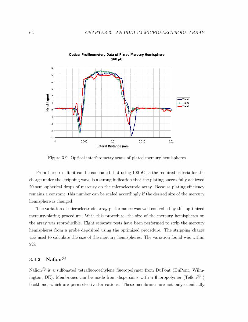
62 CHAPTER 3. AN IRIDIUM MICROELECTRODE ARRAY
Figure 3.9: Optical interferometry scans of plated mercury hemispheres
From these results it can be concluded that using 100 mC as the required criteria for the
charge under the stripping wave is a strong indication that the plating successfully achieved
20 semi-spherical drops of mercury on the microelectrode array. Because plating efficiency
remains a constant, this number can be scaled accordingly if the desired size of the mercury
hemisphere is changed.
The variation of microelectrode array performance was well controlled by this optimized
mercury-plating procedure. With this procedure, the size of the mercury hemispheres on
the array was reproducible. Eight separate tests have been performed to strip the mercury
hemispheres from a probe deposited using the optimized procedure. The stripping charge
was used to calculate the size of the mercury hemispheres. The variation found was within
2%.
3.4.2 Nafion®
Nafion® is a sulfonated tetrafluoroethylene fluoropolymer from DuPont (DuPont, Wilm-
ington, DE). Membranes can be made from dispersions with a fluoropolymer (Teflon® )
backbone, which are permselective for cations. These membranes are not only chemically

3.4. EXPERIMENTATION 63
resistant but can afford some degree of protection to the underlying materials by preventing
damaging anions from reaching the mercury surface without interfering with the transport of
the metal cations. One source of degradation is the fouling of the plated mercury electrode.
While the underlying substrate and iridium electrode are very robust, the mercury hemi-
sphere is more susceptible to attach. Chloride ions, for example, will react with mercury
and foul the electrode. These are common in many applications of interest. This property
of selective transport has been used previously to improve the performance of iridium and
silver/silver chloride electrodes for pH sensing [103].
To test Nafion®’s ability to protect against mercury degradation, probes were dip-coated
in a 5 wt.% solution of Nafion® in ethanol. Probes were then air dried, followed by a 12 h
anneal at 80 °C. Trials were run in test solutions that were then spiked with 100 ml aliquots
of 0.1M HCl to a concentration of 1mM. Comparisons of scans before and after spiking for
bare mercury and Nafion®-coated probes were examined.
Results with Nafion® were inconclusive. Mercury plating was successful on coated
probes (i.e. through the coating). Results comparable to uncoated probes were obtained for
scans of 50 ppb Cu+2 in both HF and perchloric acid. However, when an electrochemical
cell with 50:1 HF was poisoned with 1mM HCl, the Nafion® coating peeled and flaked off
the surface after roughly 18 hours of exposure. These flakes did not dissolve in solution,
indicating that the HCl attacked the interface between the Nafion® and the probe. More
work would be necessary to improve the quality of the coating for it to be of use with the
chemistries that were tried.
3.4.3 Element Screening
An investigation of the metalic elements suitable for analysis by SWASV was carried out.
Eighteen common elements were tested: Al, As, Bi, Cd, Cr, Cu, Ge, In, Mg, Mn, Ni, Pb, Pt,
Sb, Sn, Ti, Tl and Zn. Tests were done under a standard set of conditions: 15 minute pre-
concentration at -1.2V vs. Ag/AgCl in 50 ppb single element solution. The solutions tested
were 0.1M of perchloric (HClO4), nitric (HNO3), sulfuric (H2SO4), phosphoric (H3PO4),
hyrdochloric (HCl) acids and a 50:1 solution of HF.
Results are summarized in Table 3.3. Among the eighteen elements, only Bi, Cd, Cu,
Pb, Sb, Tl and Zn showed positive responses in the 6 types of diluted process chemicals and
are therefore suitable for the ASV technique.

64 CHAPTER 3. AN IRIDIUM MICROELECTRODE ARRAY
Table 3.3: Element screening by SWASV
Element 0.1MHClO4
0.1MHNO3
0.1MH2SO4
0.1MH3PO4
0.1MHCl
50:1HF
Al - - - - -As - - - - -Bi - Cd Cr - - - - -Cu Ga -Ge - -In - G# - -Mg - - - -Mn - - -Ni - - - -Pb Pt - -Sb - G# G#Sn - - - - G#Ti - - - -Tl -Zn
- DetectableG# - Detectable but low sensitivity- - Not detectable
3.4.4 Operation in HF
The ultimate goal of this project was to demonstrate the surviveability in a media that would
not have been possible without the addition of PECVD silicon carbide. 50:1 hydrofluoric
acid (HF) was chosen because of previous failures with PECVD silicon dioxide and silicon
nitride and the interest in monitoring semiconductor processing fluids. Normal probes that
have been insulated with some form of silicon dioxide have a very limited lifetime in HF.
The etch rate of a densified low-temperature oxide (LTO) in 50:1 HF has been reported as
8.7 nm/min [4]. An electrode array with 1 µm of oxide would last just under 2 h before the
metal traces would be exposed.
As a first demonstration, the measurement-to-measurement variation was characterized
by performing repeat analysis using the same Hg-microelectrode array in every ten minutes

3.4. EXPERIMENTATION 65
in a 50:1 HF solution. The solution was continuously stirred to ensure homogeneity. At the
preconcentration step, a -1.2V vs. Ag/AgCl was applied for 4minutes. It was followed by a
square wave anodic potential sweep from -1.2 V to -0.1 V. The frequency of the square wave
signal was 60Hz. The probe was allowed to rest for 5min before the start of another cycle
of analysis. After one hour, the solution was spiked with 50 ppb Cu+2. After approximately
11 h of continuous operation, the solution was spiked again with an additional 10 ppb Cu+2.
The initial background charging current observed was 17 nA. After the spiking to 50 ppb,
the current showed an immediate increase to approximately 260 nA. This corresponds to
about 4.84 nA/ppb. After the additional spike the current jumped to about 313 nA, corre-
sponding to 4.93 nA/ppb. The stripping current was stable and repeatable with a variation
of ±1.8% over the time period examined. The data from the trial is plotted in Figure 3.10.
Figure 3.10: Repeatability of ASV analysis over 70 hours
A longer reproducibility study was also carried out. Two probes were soaked in 50:1
HF solution for four days. In the beginning of this period, stripping currents in 50 ppb
Cu+2 solution were collected. During the four day period, one probe was allowed to soak
undisturbed in the solution while the other was repeatedly cycled through a SWASV analysis.
Stripping currents after this period were collected under the same conditions. Results are
shown in Table 3.4.

66 CHAPTER 3. AN IRIDIUM MICROELECTRODE ARRAY
Probe Soaking Condition Stripping Current Initial (nA) Stripping Current Final (nA)A Rest 220 190B Repeatedly Scanned 193 240
Table 3.4: Four-day exposure to 50:1 HF
The probe at rest showed a change of 13.6% while the probe run repeatedly showed a
change of 24%. While it might be desirable to improve the repeatability through development
of more advanced electrochemical techniques, the performance is sufficient for contamination
detection of a process bath. No degradation of the probe itself could be detected, either
from behavior during the analysis or under microscopic examination.
3.5 Summary
The previously published fabrication process for the microelectrode array was successfully
modified to improve the reliability of the thin-film iridium electrodes. The addition of
PECVD carbide as the outer dielectric enabled the successful demonstration for extended
periods of time in 50:1 HF. The plating process was optimized to improve repeatability
and develop criteria for determining the quality of both the microelectrode array and the
plated mercury hemisphere. Basic analysis parameters were investigated and then applied
to a broad range of elements and solutions to show which could be detected by the SWASV
method. The repeatability and viability for several days of exposure in 50:1 HF were demon-
strated.
While the use of the sensor in HF was demonstrated, future work should focus on the
development of an electrochemical system to practically deploy the sensor into an applica-
tion. Such a system would include the electronics (potentiostat, control systems) and some
form of sampling such as a flow cell. Additionally, modifications to the classical technique
of SWASV may be necessary to improve the repeatability and robustness of the system.

Chapter 4
Microfluidic Gaskets
Introduction
In developing a microfluidic system for a particular application, a designer might wish to
choose and control the materials with which the fluids of interest come into contact. It
may be that a reaction can be altered by certain surfaces. It could also be that chemicals
present can attack or corrode components of the fluidic system if they are not suitably
protected. To broaden the usefulness of microfluidic systems in general, a technique of
coating channels during fabrication was conceived and developed. This work focused on
making them chemically inert, but the approach has potential in other applications (e.g.
chromatography, electrophoresis, etc.) where the role of the channel surface is more involved
with the function of the device.
4.1 Self-sealing Microfluidic Channels
An initial approach to achieve a chemically resistant microfluidic channel relied on a fab-
rication process that was both coating and self-sealing in the same process step. The idea
was originally developed by Nick Mourlas at Stanford University. An oxide mask was used
during an isotropic SF6 plasma etch. The etch undercut the mask and defined the geometry
of the channel’s cross section. A thin film was then deposited (PECVD silicon carbide in this
case). The deposition process produced a film conformal enough that the the interior walls
of the channel were coated before the channel was sealed. A cross-section of the process flow
is shown in Figure 4.1.
67

68 CHAPTER 4. MICROFLUIDIC GASKETS
(a) Silicon channel is etched isotropically un-der an oxide mask
(b) PECVD silicon carbide is deposited untilwalls are coated and channel is sealed.
Figure 4.1: Self-sealing microfluidic channel process
The size of the mask opening is critical for proper coating and sealing. If the channel
is wider than 4 mm it is difficult to seal with a PECVD film; however, too narrow a mask
opening results in a channel that is sealed before a sufficiently thick conformal coating is
deposited on its internal surfaces. Figure 4.2 shows a channel that was etched with SF6
for 100minutes, with a flow rate of 150 sccm of SF6, at a pressure of 100mTorr, and power
of 550W in a Drytek D-100 plasma etcher with six electrodes of 232 cm2 each. A 3.8 mm
PECVD silicon carbide film was then used to coat and seal the channel. After dicing, a
1minute etch in 49% HF at room temperature and 1minute in 45% KOH at 80 °C were used
to highlight the SiO2/SiC/Si interfaces. The coating was nominally conformal; its minimum
thickness was approximately 200 nm. The fact that the channel wall deposition rate was
significantly smaller than the surface deposition rate dictates that a thorough understanding
of the deposition characteristics will be necessary to identify the dimension limits to produce
conformal coatings with sealed channels.
Self-sealed channels proved to be an impractical exercise. The geometry of closed chan-
nels is severely limited to sizes that can be anisotropically etched under a gap between 3
and 4 mm wide. The limitation on size and delicate structure of the top membrane makes
a practical solution for coupling to the channel difficult. Also, the region where the seal
comes together is very narrow and likely to create a dead volume fluids flowing through
the channel. For these reasons, another solution to making chemically inert channels was
developed.

4.2. GASKET PROCESS 69
Figure 4.2: The image on the left shows a cross-section of a self-sealing microfluidic channel.The close up on the right shows a conformal coating in the corner of the channel.
4.2 Gasket Process
Existing approaches to fabricating fluidic channels typically involve patterning into a sub-
strate (silicon or PDMS is commonly used) and then bonding with a cap wafer (e.g. Pyrex®).
Attempts were made to bond PECVD silicon carbide by both anodic and fusion bonding.
None of these attempts were successful. Consequently, a more versatile method was devel-
oped to fabricate a fluidic channel where all the materials present would be inert relative to
a broad range of chemistries.
Figure 4.3: Concept of a microfluidic gasket
The process first involved depositing PECVD silicon carbide on the etched channels and
surface of the wafer. Using dry film lithography (discussed next), a process flow was devised
that enabled the patterning of the carbide near the edge of the channel, leaving the coating

70 CHAPTER 4. MICROFLUIDIC GASKETS
intact. Bonding around this patterned feature with a mating surface formed a microfluidic
gasket, sealing the channel by compression. A conceptual diagram is shown in Figure 4.3.
The gasket process was adapted for use in a flow-through total organic carbon sensor that
is discussed in more detail in Chapter 5.
One of the challenges in the proposed process flow is the required step of patterning back
the coating within a specified distance of the channel. Several alternatives were investigated
including spray film resists, CVD photoresist, and alternative coating techniques. A process
flow that took advantage of a dry film resist appeared most promising and was eventually
chosen as the best approach.
4.2.1 Dry Film Lithography
Previous work had been published that successfully demonstrated the use of dry film pho-
toresist in MEMS [104]. After review of the available materials and discussions with Martin
Hill of DuPont’s technical support group (E.I. DuPont de Nemours & Co., Research Trian-
gle Park, NC), two different formulations of Riston® were evaluated: SF125 and CM206.
CM206 was chosen as the best candidate because of its lower thickness. At 15 mm, it had
the potential to achieve the highest resolution of the dry film resists available. Riston® is
designed for automated printed circuit board manufacturing. Adapting it to MEMS fab-
rication required a number of modifications and optimizations from the standard process
flow.
Figure 4.4: Trilayer Riston® film
4.2.1.1 Lamination
Riston® is a trilayer laminated photosensitive film. The photosensitive layer is sandwiched
between two layers of transparent mylar as shown in Figure 4.4. In typical PC board

4.2. GASKET PROCESS 71
fabrication, the bottom layer of mylar is removed and the Riston® is exposed through the
top layer of mylar. The lamination, exposure, and development are done in an automated
conveyor system that is unsuitable for wafers. For this work, a standard identification
card laminator was adapted for use in the clean room. To support the wafer as it passed
through the laminator, a custom aluminum wafer carrier was designed with a 250 mm recess.
During the lamination process, the wafer was placed into the carrier. The bottom mylar was
removed from a sheet of Riston® and manually tensioned over the carrier and wafer. The
three layers, aluminum carrier, wafer, and Riston® sheet were then fed into the laminator
together.
Initial results showed that adhesion of Riston® to bare silicon and wafers coated with
silicon carbide was marginal. Films delaminated very easily, often when pulling off the top
layer of mylar. To achieve adequate adhesion, Riston® required heating the substrate either
during or after lamination, and deposition of a thin layer of metal. Because Riston® can
polymerize over 110 °C and the laminator did not have precise temperature control, wafers
were heated on a hot plate at 90 °C for 1min after lamination with a weight applied to the
mylar surface. Choosing a metal layer required screening potential candidates against the
planned processing later in the flow. The etchant used to pattern the adhesion layer must
not damage the Riston®, nor should the developer for Riston® undercut and damage the
adhesion layer. To avoid this potential incompatibility, combinations of Riston®, aluminum,
and chromium, and chromium/gold were tested against different etchants. Based on the
results from these tests shown in Table 4.2, a thin layer of chromium was selected as the
best choice for an adhesion layer.
4.2.1.2 Exposure
The top mylar sheet diffuses light and sets a limit in proximity of the mask to the photo-
sensitive layer of about 25 mm. In an attempt to improve resolution, the mylar was removed
and the mask was exposed in contact with the photosensitive layer. The Riston® stuck to
the mask so tenaciously that even after a long attempt to remove it in various strippers
the wafer could not be removed without damaging the mask. Polyvinyl alcohol (PVA) was
suggested by Martin Hill from DuPont as a spin on barrier layer that would allow intimate
contact without sticking and not interfere with the exposure or development of the film.
Because PVA does not dissolve readily in deionized (DI) water at room temperature,
preparation of a 10% solution required heating the solution to 50 °C for a several hours. Once
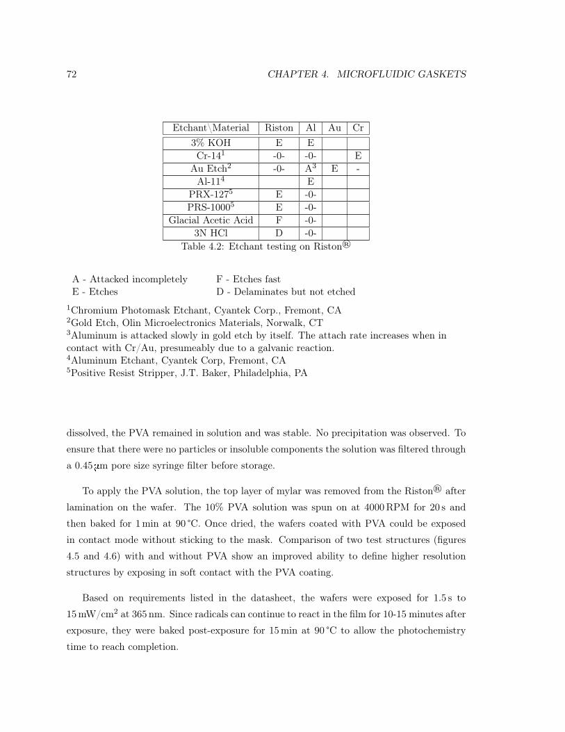
72 CHAPTER 4. MICROFLUIDIC GASKETS
Etchant\Material Riston Al Au Cr3% KOH E ECr-141 -0- -0- E
Au Etch2 -0- A3 E -Al-114 E
PRX-1275 E -0-PRS-10005 E -0-
Glacial Acetic Acid F -0-3N HCl D -0-
Table 4.2: Etchant testing on Riston®
A - Attacked incompletely F - Etches fastE - Etches D - Delaminates but not etched
1Chromium Photomask Etchant, Cyantek Corp., Fremont, CA2Gold Etch, Olin Microelectronics Materials, Norwalk, CT3Aluminum is attacked slowly in gold etch by itself. The attach rate increases when incontact with Cr/Au, presumeably due to a galvanic reaction.4Aluminum Etchant, Cyantek Corp, Fremont, CA5Positive Resist Stripper, J.T. Baker, Philadelphia, PA
dissolved, the PVA remained in solution and was stable. No precipitation was observed. To
ensure that there were no particles or insoluble components the solution was filtered through
a 0.45 mm pore size syringe filter before storage.
To apply the PVA solution, the top layer of mylar was removed from the Riston® after
lamination on the wafer. The 10% PVA solution was spun on at 4000RPM for 20 s and
then baked for 1min at 90 °C. Once dried, the wafers coated with PVA could be exposed
in contact mode without sticking to the mask. Comparison of two test structures (figures
4.5 and 4.6) with and without PVA show an improved ability to define higher resolution
structures by exposing in soft contact with the PVA coating.
Based on requirements listed in the datasheet, the wafers were exposed for 1.5 s to
15mW/cm2 at 365 nm. Since radicals can continue to react in the film for 10-15 minutes after
exposure, they were baked post-exposure for 15min at 90 °C to allow the photochemistry
time to reach completion.

4.2. GASKET PROCESS 73
Figure 4.5: Serpentine with no PVA Figure 4.6: Serpentine with PVA
4.2.1.3 Development
In the first series of experiments, the wafers were rinsed in DI water to remove the PVA prior
to development, and to rinse away the developer after development. Exposure to DI water
caused Riston® to swell around the edges and fine features to delaminate. The datasheet
calls for rinsing in hard water, defined as containing an equivalent of 150-250 ppm CaCO3,
making it likely that the root cause behind this effect was the relatively high osmotic pressure
of DI water on the film. Adding 150 ppm of MgSO4 to DI water for rinsing was successful
at eliminating the swelling. After several more trials, no adverse affects were observed by
going straight into the developer after exposure and bake without rinsing the PVA, and the
first rinse was eliminated from the process flow.
Figure 4.7: Edge swelling after rinse in DI wa-ter
Initial trials using a tank develop proved
unsatisfactory. Development proceeded
slowly and unevenly. In most cases the pat-
tern failed to completely resolve. In typical
applications, the Riston® is passed through
an automated conveyor that sprays on de-
veloper under pressure. The datasheet calls
for a spray pressure of 140 kPa to 210 kPa.
Evidently the mechanical abrasion of the
pressured developer is a necessary compo-
nent in the removal of the exposed resist

74 CHAPTER 4. MICROFLUIDIC GASKETS
material. To achieve satisfactory results, a custom pressure spray developer was designed
as shown diagrammatically in Figure 4.8.
Figure 4.8: Customized pressure spray developer
While the spray development was an improvement over the tank development, residues
and particles were still observed in some open areas and on the edges. The pressure in the
hand system was limited and possibly insufficient to properly clear exposed areas. Fortu-
nately an oxygen plasma descum proved very effective at improving the definition of features
and removing any lingering residue. Wafers were cleaned up using an MRCModel 55 reactive
ion etching system (Materials Research Corporation, Orangeburg, NY), 25 sccm, 25mTorr,
100W, for 15min. Images of a test feature before and after descum are shown in Figure 4.9.
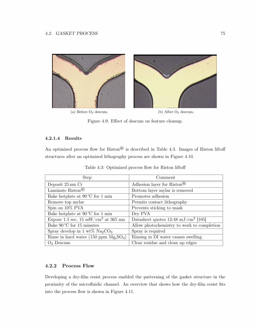
4.2. GASKET PROCESS 75
(a) Before O2 descum. (b) After O2 descum.
Figure 4.9: Effect of descum on feature cleanup.
4.2.1.4 Results
An optimized process flow for Riston® is described in Table 4.3. Images of Riston liftoff
structures after an optimized lithography process are shown in Figure 4.10.
Table 4.3: Optimized process flow for Riston liftoff
Step CommentDeposit 25 nm Cr Adhesion layer for Riston®
Laminate Riston® Bottom layer mylar is removedBake hotplate at 90 °C for 1 min Promotes adhesionRemove top mylar Permits contact lithographySpin on 10% PVA Prevents sticking to maskBake hotplate at 90 °C for 1 min Dry PVAExpose 1.5 sec, 15 mW/cm2 at 365 nm Datasheet quotes 12-48 mJ/cm2 [105]Bake 90 °C for 15 minutes Allow photochemistry to work to completionSpray develop in 1 wt% Na2CO3 Spray is requiredRinse in hard water (150 ppm MgsSO4) Rinsing in DI water causes swellingO2 Descum Clear residue and clean up edges
4.2.2 Process Flow
Developing a dry-film resist process enabled the patterning of the gasket structure in the
proximity of the microfluidic channel. An overview that shows how the dry-film resist fits
into the process flow is shown in Figure 4.11.

76 CHAPTER 4. MICROFLUIDIC GASKETS
Figure 4.10: Patterned Riston® in proximity to channel
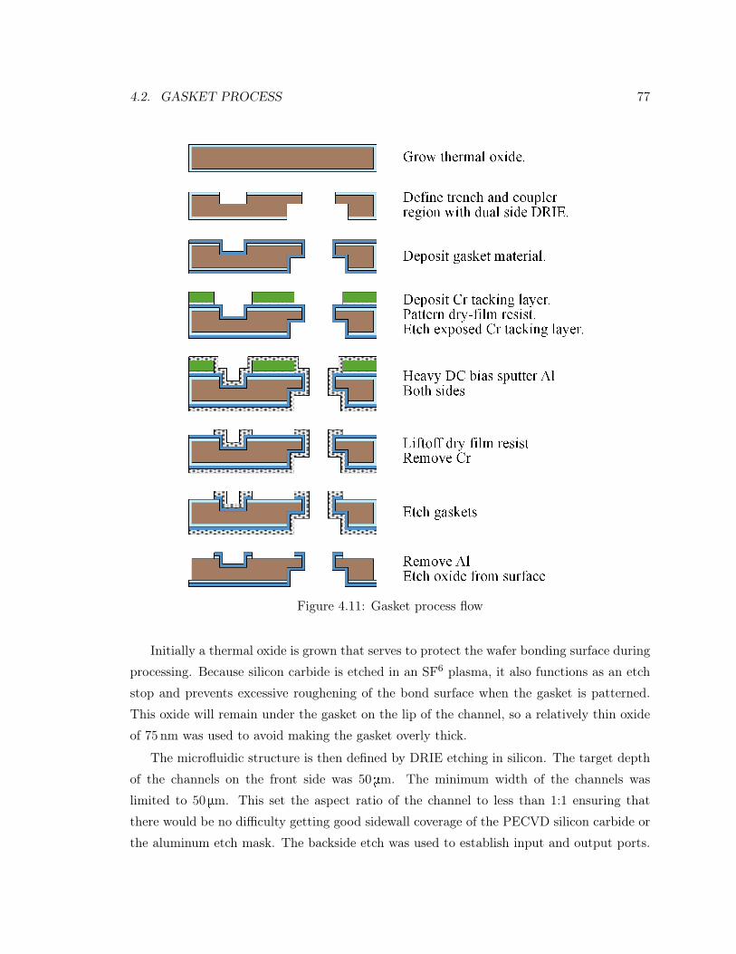
4.2. GASKET PROCESS 77
Figure 4.11: Gasket process flow
Initially a thermal oxide is grown that serves to protect the wafer bonding surface during
processing. Because silicon carbide is etched in an SF6 plasma, it also functions as an etch
stop and prevents excessive roughening of the bond surface when the gasket is patterned.
This oxide will remain under the gasket on the lip of the channel, so a relatively thin oxide
of 75 nm was used to avoid making the gasket overly thick.
The microfluidic structure is then defined by DRIE etching in silicon. The target depth
of the channels on the front side was 50 mm. The minimum width of the channels was
limited to 50 mm. This set the aspect ratio of the channel to less than 1:1 ensuring that
there would be no difficulty getting good sidewall coverage of the PECVD silicon carbide or
the aluminum etch mask. The backside etch was used to establish input and output ports.

78 CHAPTER 4. MICROFLUIDIC GASKETS
The etch depth was sufficient to connect to the microfluidic channel while leaving sufficient
material for the fluidic coupler.
The gasket material, 350 nm of PECVD silicon carbide in this case, was deposited on
both sides of the wafer using 2000 sccm of SiH4, 1440 sccm of CH4 at 1300mTorr with 3 s
of high-frequency power and 3 s of low-frequency power both at 100W. The trials with the
self-sealed channels (Section 4.1) demonstrated that good coverage on the side walls would
be achieved.
After the carbide, a 35 nm layer of chromium was deposited to improve the adhesion of
the dry-film resist as described in Section 4.2.1. After the process for the dry-film resist, the
chromium layer was removed in the exposed areas by etching for 5 min. At this point, the
wafers were ready for a deposition of the aluminum mask layer.
In order to ensure good sidewall coverage, the sputter deposition of the aluminum mask
was done with a heavy DC bias. A DC bias during deposition promotes substrate sputtering
and redeposition which promotes conformality [106]. To further ensure that the carbide
coating would be protected by the aluminum mask, an extra thick layer was deposited.
Wafers were deposited at Lance Goddard Associates (Foster City, CA); 2 mm was deposited
on the front side, 1.5 mm on the back side.
The mask was lifted off with PRX-127 which had been tested to be effective at removing
Riston® without damaging the aluminum. For fine features, a bi-layer liftoff structure is
preferred, but because the edge of the gasket is not a critical, any roughness or jagged edge
was acceptable. A SEM of the aluminum mask is shown in Figure 4.12.
Figure 4.12: Shown are SEM’s of aluminum mask structure: top view, upper corner, andlower corner.

4.2. GASKET PROCESS 79
Once the Riston® was removed, the underlying chromium adhesion layer was removed
using CR-14. The remaining aluminum mask protected the carbide gaskets and the coating
in the channel and ports. The carbide was etched in in Drytek Model D-100 reactive ion
etcher (Drytek, Inc., Wilmington, MA) using SF6 at 50 sccm, C2ClF5 at 70 sccm, 100mTorr,
55W. The etch time was 5:30min.The final step is a short etch in 6:1 buffered oxide etch
(BOE) to remove the underlying oxide etch. The wafer is now ready for anodic bonding
with the glass substrate. The patterned gasket is shown in Figure 4.13.
Figure 4.13: SEMs of carbide gasket
4.2.3 Glass wafer
The process for the glass wafer is relatively simple and shown in Figure 4.14. PECVD silicon
carbide was deposited on a double-side polished Pyrex® 7740 wafer in a mirror image to the
gasket pattern on the silicon with the microfluidic channels. The two wafers were bonded
at 350 °C with 600N of force, ramping to 1200V in 100V increments. A cross-section of the

80 CHAPTER 4. MICROFLUIDIC GASKETS
resulting structure is shown in Figure 4.15.
Figure 4.14: Process flow for glass wafer
Figure 4.15: Cross-section of gasket structure
4.3 Summary
A gasket structure was proposed that enables the fabrication of microfluidic channels with a
uniform coating. Several processing challenges were overcome related to lithography in the
region of the channels. The gasket process was adapted for use in a total organic carbon
sensor and is discussed in Chapter 5.

Chapter 5
Total Organic Carbon Sensor
Introduction
In several diverse areas there is a need for a non-specific total organic carbon sensor (TOC).
In semiconductor and pharmaceutical manufacturing, the specific analytes are well-known
because the possible constituents are tightly controlled. In this instance a non-specific TOC
sensor can have benefits over a slower, more expensive chemical-specific measurement tech-
nique. Examples are waste water monitoring for photoresist or pharmacological precursors.
In environmental monitoring where the specific nature of the contaminant is not known, a
non-specific TOC sensor can monitor for an entire class of contaminants without the need to
know their exact chemistry. A specific example is the use of TOC analysis to determine the
amount of bacteria in ground water. An overview of TOC sensing can be found in reports
that have been published by the U.S. Environmental Protection Agency [107,108].
Conventional TOC measurement techniques involve a two-step process. In the first
phase, the organic carbon is oxidized. The objective is to convert all organically bound
carbon into carbon dioxide (CO2 ). By converting all carbon into this form, detection
method can be used in the second phase to detect the CO2. Because all carbon is oxidized
to this form regardless of its precursor, the detection method can be optimized for a single
analyte.
Typical benchtop models are shown in Figure 5.2. One approach in this class of TOC
sensors is to oxidize the organic carbon via high temperature combustion (e.g. 1200 °C),
and then pass the resulting CO2 into a cell where a change in conductivity is measured.
The cost of these units is typically $18,000 to $24,000. In some applications it would be
81

82 CHAPTER 5. TOTAL ORGANIC CARBON SENSOR
Figure 5.1: Current TOC sensing methodology
desirable to monitor in-situ to prevent the accidental discharge of harmful chemicals, or avoid
contaminating a drinking water supply. These types of applications present a challenge for
the conventional units because of power, size, and cost requirements.
Figure 5.2: Sievers 900 benchtop TOC sensor (General Electric Company, Schenectady, NY)
Fortunately these are three areas in which a microfluidic approach to TOC sensing would
have several advantages. The size and cost advantages are inherent. The power requirement
can be addressed by resorting to an ultra-violet (UV) catalyzed oxidation along with a
differential pH sensing approach, described next. This greatly reduces the power required
to the point where a hand-held unit that would run for a reasonable time from a battery
source would be feasible. Sensing in remote locations would be possible without the need for
returning samples to a lab. This would eliminate the delay in results and the contamination
risks that bringing samples back for analysis entails.

5.1. THEORY 83
Thanks are due to Dr. Dolf Van der Heide for assistance with the FEA modeling.
5.1 Theory
To be rigorous, pH was originally defined in 1909 [109] as
pH = −log10([H+])
(5.1)
where [H+] is the molar concentration of the hydrogen ion. Often the hydronimum ion
[H3O+] is used instead if [H+], acknowledging that the hydrogen ion can protonate a water
molecule. pH was later defined to include the relative activity of hydrogen ions as
pH = −log10(mHγH
m0
)(5.2)
where
• mH is the concentration of the hydrogen ion as molality,
• gH is the molal activity coefficient, and
• m0 is the standard molality.
The activity coefficient takes into account the fact that in solution there is an interaction
between ions that can cause them to exhibit an effective concentration that deviates from
an ideal solution (where there is no interaction). Except for concentrated solutions, the
activity coefficient of hydrogen ions is essentially 1. To simplify calculations, equation 5.1
will be used.
5.1.1 Concept
The approach taken for a microfluidic, flow-through TOC sensor is to first mix the analyte
with a known volume and concentration of oxidizing species. The oxidizer should have a
reactivity that readily oxidizes the organic carbon in the presence of ultra-violet light, but
does not react without it. The analyte stream is split into two channels. One is exposed to
UV light, the other is shielded. The two streams pass over matched pH sensitive electrodes
and the pH change is sensed differentially. A conceptual drawing of the microfluidic structure
is shown in Figure 5.3.

84 CHAPTER 5. TOTAL ORGANIC CARBON SENSOR
Figure 5.3: Conceptual drawing of TOC sensor
5.1.2 Analytical Model
Organic molecules can be oxidized in the presence of oxygen to form carbon dioxide (CO2).
In an aqueous environment, CO2 reacts with water to form carbonic acid (H2CO3), which
causes a pH change in solution. The total organic carbon (TOC) sensor relies on sensing
this pH change to determine the amount of organic carbon originally present in solution.
Unlike commercially available TOC sensing systems that rely on measuring an absolute
change in pH, the differential TOC measures the difference in pH between two matched
channels. In one channel, ultraviolet light drives the oxidation of the organic carbon. The
other channel, the reference channel, is shielded from the UV light, and the oxidation of
the carbon does not proceed during the travel time of the analyte through the system. The
same advantages that apply to a differential amplifier are present here: high common mode
rejection and large possible gain.
Ideally, the intensity of the UV light should be high enough that all forms of organic
molecules are completely oxidized. The oxidizer should be sufficiently weak that without
the UV catalysis it does not react significantly with the hydrocarbon.
In its simplest representation, the complete oxidation of a simple alkane hydrocarbon
form can be shown as
CNH2N+1 + (3N + 1)O −−−−→ CO2 + (N + 1)H2O (5.3)
The above reaction is an oversimplification and can involve several different intermedi-
ates depending upon the oxidizing agents or catalysts present in solution. However, because

5.1. THEORY 85
intermediates are generally ephemeral in nature and the end result of the carbon oxida-
tion is the same, this oversimplification is useful for generating a predictive model for the
performance of an in-line TOC sensor.
Carbon dioxide is readily soluble in water, roughly 39mM/l at 20 ºC. A percentage of
the resulting CO2 reacts with water to form carbonic acid:
CO2 +H2Okh−−−−−−−−−− H2CO3 (5.4)
Carbonic acid is a diprotic acid and dissociates in two stages with two distinct dissocia-
tion constants.
H2CO3k1−−−−−−−−−− H+ +HCO−
3
k2−−−−−−−−−− 2H+ +CO−23 (5.5)
where k1 and k2 are the dissociation constants defined as
k1 =[H+]
[HCO−
3
][H2CO3]
(5.6)
and
k2 =[H+]
[CO−
3
][HCO−
3
] (5.7)
In order to derive a model for the pH response of the TOC system, it is also necessary
to take into account the following relationships:
koxCT =[CO2] +[CO−2
2
]+[HCO−
3
]+ [H2CO3] (5.8)
[H+]×[OH−] = kw (5.9)
[H+]=[OH−]+ [HCO−
3
]+ 2
[CO−2
3
](5.10)
where
CT is the initial total concentration of organic carbon,
kox is the percentage of carbon that oxidizes, and
kw is the dissociation constant of water.

86 CHAPTER 5. TOTAL ORGANIC CARBON SENSOR
Equation 5.10 is the charge balance equation and must be satisfied to ensure charge
neutrality. Equations 5.4 through 5.10 comprise a system of six equations with six unknowns
and all degrees of freedom are satisfied to derive a solution.
Combining equations 5.4, 5.6 and 5.7 with equation 5.8 yields
[CO−2
3
]= k1k2
[H2CO3]
[H+]2(5.11)
Substituting equations 5.6 and 5.11 into equation 5.8 yields
koxCT =[H2CO3]
kh+
k1k2 [H2CO3]
[H+]2+
k1 [H2CO3]
[H+]+ [H2CO3]
= [H2CO3]
([H+]
2+ k1k2kh + k1kh [H
+] + kh [H+]
2
kh [H+]2
)
Rearranging and solving for [H2CO3],
[H2CO3] = koxCTkh [H
+]2
[H+]2 + kh [H+]2 + k1kh [H+] + k1k2kh(5.12)
Substituting equations 5.12, 5.6, and 5.11 into the charge balance equation 5.10 yields
[H+]− kw
[H+]−(
k1[H+]
+2k1k2
[H+]2
)[koxCTkh [H
+]2
[H+]2 + kh [H+]2 + k1kh [H+] + k1k2kh
]= 0
[(1 + kh)
[H+]4
+ k1kh[H+]3
+ (k1k2kh − kw − kwkh − k1khkoxCT )[H+]2
−(kwk1kh + 2k1k2khkoxCT )[H+]−k1k2kwkh
]1
[H+]2 + kh [H+]2 + k1kh [H+] + k1k2kh= 0
Because we are only interested in non-zero, positive, real roots of the equation, the
numerator must be zero.

5.1. THEORY 87
(1 + kh)[H+]4
+ k1kh[H+]3
+ (k1k2kh − kw − kwkh − k1khkoxCT )[H+]2
− (kwk1kh + 2k1k2khkoxCT )[H+]− k1k2kwkh = 0
At 20 ºC, k1= 4.2 x 10⁻⁷, k2= 4.8 x 10⁻¹¹, and kh=1.3 x 10⁻³. The second dissociation
lags four orders of magnitude behind the first and is generally disregarded for the pH effect
of dissolved CO2. There is now sufficient information to predict an expected pH shift due
to oxidation of organic carbon within a TOC sensor. The results are shown in Figure 5.4.
Figure 5.4: Theoretical pH shift due to TOC concentration
From the model, the method of pH sensing in an aqueous environment is limited by
the equilibrium between [CO2] and [H2CO3] and the dissociation of water. The amount of
[H2CO3] has to be above the ambient concentration of [H+].

88 CHAPTER 5. TOTAL ORGANIC CARBON SENSOR
5.2 Benchtop Model
Before fabricating a microfluidic version, a benchtop version of the differential, flow-through
TOC sensor was fabricated to validate the differential approach and perform preliminary
tests. Quartz tubes were fabricated with inlets for iridium wire electrodes. This provided
a mechanism to evaluate different choices as an oxidizer. An initial candidate, sodium per-
sulfate, acidified the solution and caused a parasitic signal when it dissociated. The second
choice, hydrogen peroxide, proved to be more suitable for UV-photocatalytic oxidation. This
effect was not observed. Experimental parameters like UV intensity and flow speed, initial
carbon content, as well as hydrogen peroxide concentration were investigated to provide a set
of experimental conditions that would behave as expected. In this way, first concentration
dependence measurements were carried out for ethanol dissolved in DI water.
5.2.1 Experiment
The solution was pumped through the tube using a peristaltic pump. The flow speed was
approximately 1.3ml/min as determined by the droplet formation rate and frequency at the
outlet. The passage through the tube was above 10 min. The sample solution was irradiated
using two Raypen UV mercury lamps.
Sample solutions were prepared by sparging DI water with nitrogen to remove oxygen
and carbon dioxide from the solution. Next, 3.5ml/l hydrogen peroxide was added as the
oxidant. Varying concentrations of ethanol were added to separate beakers and the tube
moved from beaker to beaker to inject the samples into the system.
5.2.2 Results
The results show a logarithmic response characteristic of the sensor typical for pH detection
schemes. The electrode response was greater than expected. Typical iridium response from
literature is -60mV/pH [110], though responses as high as -90mV/pH have been reported
[111]. The value of -90mV/pH was used in the model to compare with the data.

5.2. BENCHTOP MODEL 89
Figure 5.5: Differential voltage in benchtop TOC sensor
Figure 5.6: Response of benchtop model compared with model

90 CHAPTER 5. TOTAL ORGANIC CARBON SENSOR
5.3 Microfluidic Version
5.3.1 Design
A labeled image of the layout is shown in Figure 5.7. The fluidic channels were 30 mm
wide 50 mm deep. The serpentine loops were designed to provide additional travel time
in the channel to react with the oxidizer while being exposed to UV light. Three separate
electrodes were patterned in the channel to determine the effect of surface area on the sensor
response and provide opposing electrodes for additional experiments. The holes around the
input and output ports were designed to accommodate a microfluidic coupler (courtesy of
Nick Mourlas) [112].
Figure 5.7: Microfluidic TOC sensor
The flow in the system was expected to be laminar. This can be determined analytically
from a calculation of the Reynolds number. The Reynolds number is a useful index for any
flow system that can be used to determine whether or not a flow is laminar or turbulent. It
is defined as
Re =LV ρ
µ
where
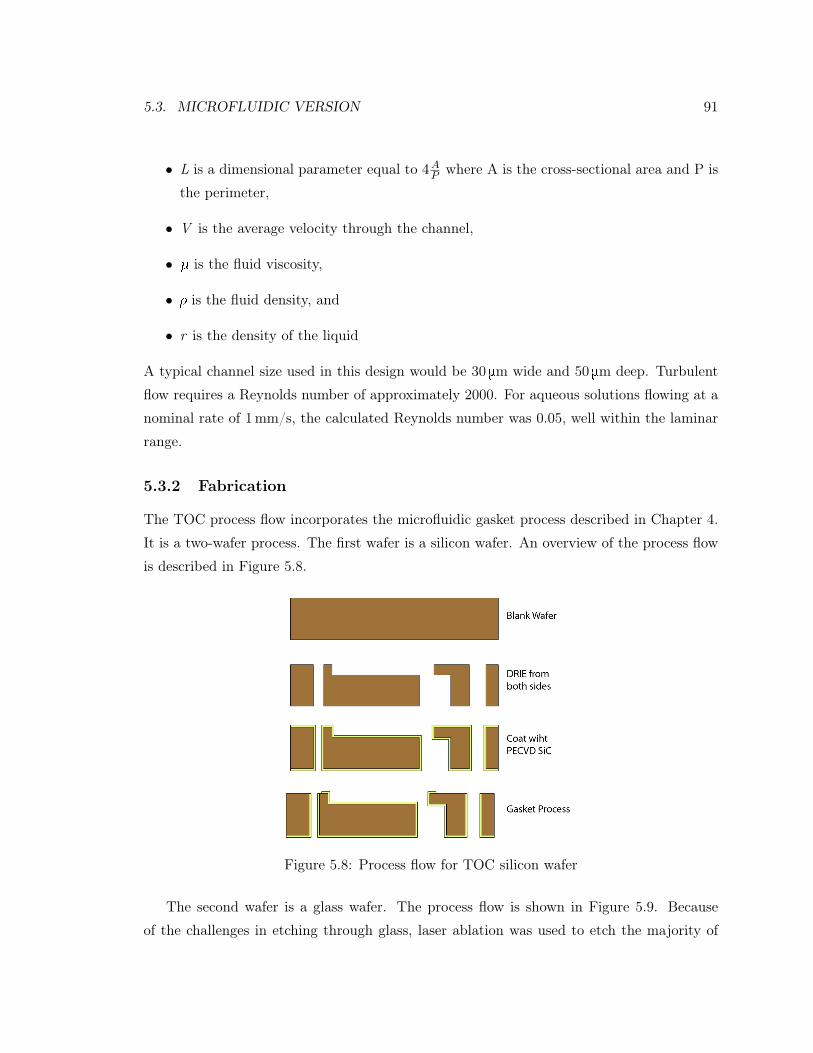
5.3. MICROFLUIDIC VERSION 91
• L is a dimensional parameter equal to 4AP where A is the cross-sectional area and P is
the perimeter,
• V is the average velocity through the channel,
• m is the fluid viscosity,
• r is the fluid density, and
• r is the density of the liquid
A typical channel size used in this design would be 30 mm wide and 50 mm deep. Turbulent
flow requires a Reynolds number of approximately 2000. For aqueous solutions flowing at a
nominal rate of 1mm/s, the calculated Reynolds number was 0.05, well within the laminar
range.
5.3.2 Fabrication
The TOC process flow incorporates the microfluidic gasket process described in Chapter 4.
It is a two-wafer process. The first wafer is a silicon wafer. An overview of the process flow
is described in Figure 5.8.
Figure 5.8: Process flow for TOC silicon wafer
The second wafer is a glass wafer. The process flow is shown in Figure 5.9. Because
of the challenges in etching through glass, laser ablation was used to etch the majority of

92 CHAPTER 5. TOTAL ORGANIC CARBON SENSOR
the way through. This greatly reduced the amount of material required for removal at the
back end to clear the holes for the heat stake couplers. The details of the laser ablation are
covered in Appendix C.
Figure 5.9: Process flow for TOC glass wafer
The glass and silicon wafer were patterned with opposing gaskets. They were aligned
and anodically bonded as shown in Figure 5.10. Once the wafers were bonded, the remaining
membrane on the glass wafer was removed mechanically, and the fluidic coupler was heat
staked into the openings. The coupler provided a means to align and seal a glass capillary
into the microfluidic channel.
Micrographs of the final channel are shown in Figure 5.11. The bond around the gasket
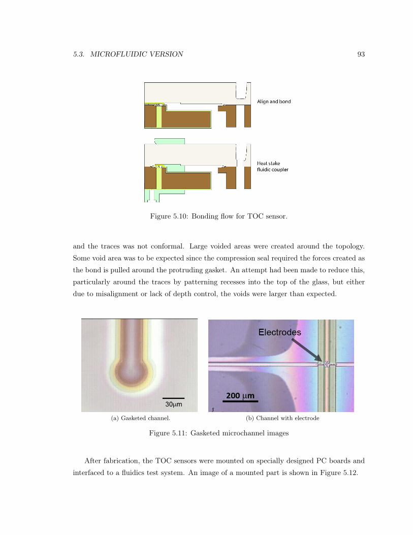
5.3. MICROFLUIDIC VERSION 93
Figure 5.10: Bonding flow for TOC sensor.
and the traces was not conformal. Large voided areas were created around the topology.
Some void area was to be expected since the compression seal required the forces created as
the bond is pulled around the protruding gasket. An attempt had been made to reduce this,
particularly around the traces by patterning recesses into the top of the glass, but either
due to misalignment or lack of depth control, the voids were larger than expected.
(a) Gasketed channel. (b) Channel with electrode
Figure 5.11: Gasketed microchannel images
After fabrication, the TOC sensors were mounted on specially designed PC boards and
interfaced to a fluidics test system. An image of a mounted part is shown in Figure 5.12.
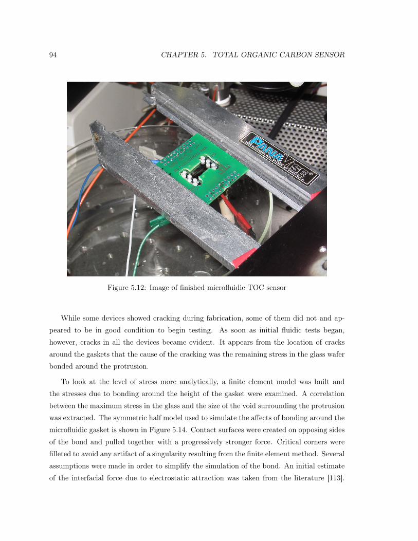
94 CHAPTER 5. TOTAL ORGANIC CARBON SENSOR
Figure 5.12: Image of finished microfluidic TOC sensor
While some devices showed cracking during fabrication, some of them did not and ap-
peared to be in good condition to begin testing. As soon as initial fluidic tests began,
however, cracks in all the devices became evident. It appears from the location of cracks
around the gaskets that the cause of the cracking was the remaining stress in the glass wafer
bonded around the protrusion.
To look at the level of stress more analytically, a finite element model was built and
the stresses due to bonding around the height of the gasket were examined. A correlation
between the maximum stress in the glass and the size of the void surrounding the protrusion
was extracted. The symmetric half model used to simulate the affects of bonding around the
microfluidic gasket is shown in Figure 5.14. Contact surfaces were created on opposing sides
of the bond and pulled together with a progressively stronger force. Critical corners were
filleted to avoid any artifact of a singularity resulting from the finite element method. Several
assumptions were made in order to simplify the simulation of the bond. An initial estimate
of the interfacial force due to electrostatic attraction was taken from the literature [113].
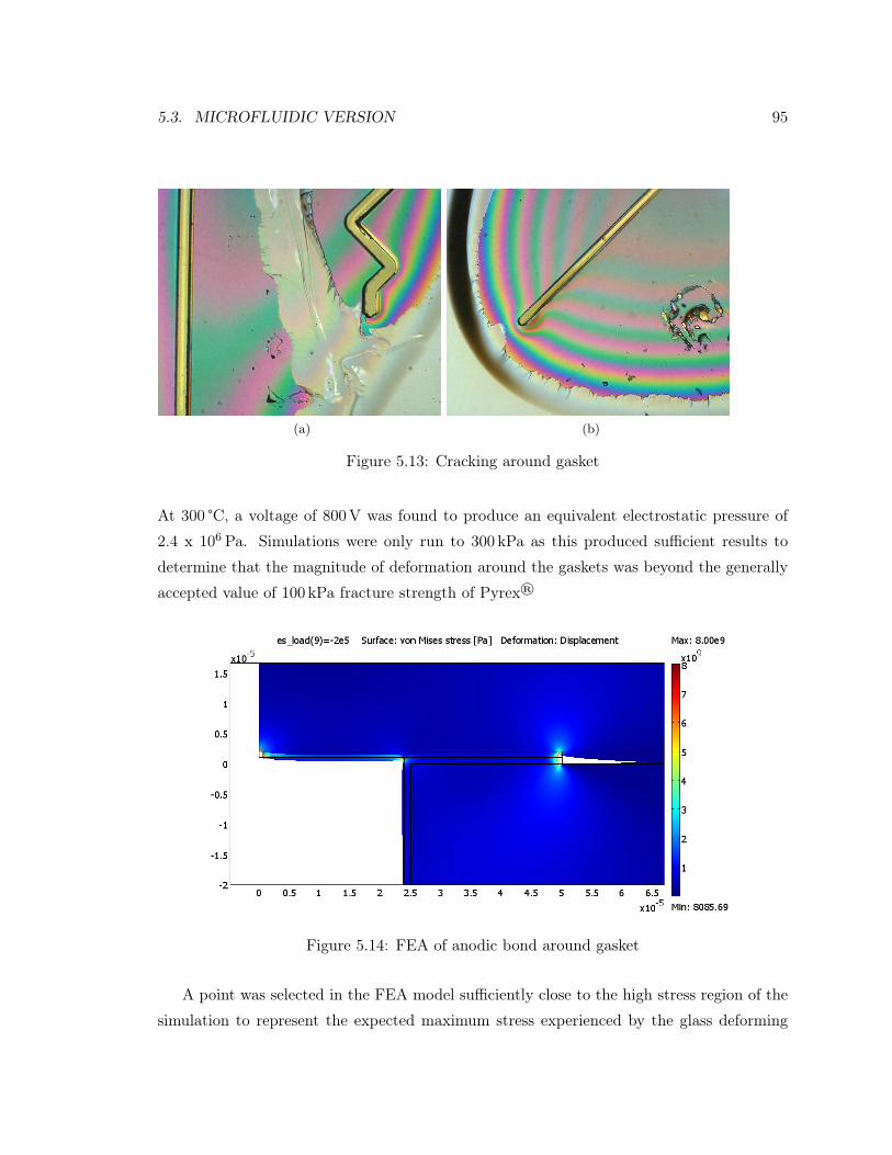
5.3. MICROFLUIDIC VERSION 95
(a) (b)
Figure 5.13: Cracking around gasket
At 300 °C, a voltage of 800V was found to produce an equivalent electrostatic pressure of
2.4 x 10⁶ Pa. Simulations were only run to 300 kPa as this produced sufficient results to
determine that the magnitude of deformation around the gaskets was beyond the generally
accepted value of 100 kPa fracture strength of Pyrex®
Figure 5.14: FEA of anodic bond around gasket
A point was selected in the FEA model sufficiently close to the high stress region of the
simulation to represent the expected maximum stress experienced by the glass deforming

96 CHAPTER 5. TOTAL ORGANIC CARBON SENSOR
around the gasket. The maximum stress was plotted against the expected distance between
the edge of the gasket and the bond front. As can be seen from the graph of Von Mises
stress vs. void distance that with a combined height of 2 mm, the bond cannot propagate
closer than several hundred microns before exceeding the fracture strength of Pyrex®. This
model is only an approximation because the exact mechanical properties of the glass wafer
at the bonding temperature are unknown. While the bond temperature of 300 °C might
provide some measure of stress relief, the anneal point for Pyrex® 7740 is 560 °C, which was
beyond the temperature limits of the bonding chamber, and above what would be desirable
from a process compatibility point of view.
Figure 5.15: Stress vs. the bonding void around the gasket
5.4 Summary
An application for the microfluidic gasket was proposed that would take advantage of the
chemical resistant nature of the channel coating. A novel methodology was proposed for
sensing the total organic carbon concentration in a flow-though, microfluidic device. The

5.4. SUMMARY 97
theory behind the sensing methodology was explored and an analytical model was developed
for predicting the sensitivity of the technique. A bench-top unit was constructed and the
technique was tested on a macroscopic scale. The data from the bench trial showed reason-
able agreement with the analytical model. A process flow for the microfluidic device was
developed and devices were fabricated. The microfluidic devices showed a common failure
mechanism due to the stress inherent in the device. An FEA model was developed and sim-
ulated to confirm the behavior. Further iteration on a design for the gasketed microfluidic
structure would allow for conditions which do not exceed the yield strength of the materials
used.
The differential pH sensor has potential applicability in any number of analytic reactions
where a pH change is the resulting indicator. The TOC sensor used light shielding to
differentiate the two analyte streams, but microfluidic systems which differentiate based on
the introduction of different reactants can also be envisioned. Specifically for application in
TOC sensing, further work in choosing a candidate for oxidation and a detailed study of the
UV catalyzed oxidation of different analytes is warranted.
Chapter 6
Conclusions and Future Work
The techniques used to deposit and grow materials during microfabrication are many and
varied: sputter deposition, reactive sputtering, e-beam and thermal evaporation, plasma
enhanced and low pressure chemical vapor deposition, epitaxial growth, molecular beam
epitaxy, and atomic layer deposition to name just some. The materials may have been stud-
ied and characterized in their classical form but, as was shown in this work, the properties
of films deposited by different methods may differ significantly. Such differences can explain
the performance of materials such as alumina, which etched unexpectedly, and the PECVD
silicon carbide, which had very different mechanical properties from its stoichiometric cousin.
As was demonstrated, chemical analysis is a valuable tool to understanding the underlying
cause behind these behavioral differences and can be used to optimize materials for their ap-
plication. The amount of Si-Si bonding produced during the PECVD deposition of carbide
is a key factor in determining carbide’s etch resistance, particularly to alkaline etchants such
as KOH. The optimized PECVD silicon carbide produced was resistant to etching in a re-
markably broad range of chemistries and yet remained compatible with standard processing
techniques.
In the area of chemical analysis, the resistance of both PECVD silicon carbide and irid-
ium were successfully demonstrated as tools to extend the range of operation for existing
electrochemical probes. The use of these materials does not necessarily require signifi-
cant modification of electrode designs. The use of an electrode array, which was previ-
ously used for analysis of tap and ground water, was successful extended into more caustic
chemistries. Such capabilities create an exciting opportunity for the development of analyses
in chemistries that have not previously been possible. The results of these experiments show
98
99
that future work may be required to develop the system level support necessary for com-
mercial deployment. Some specific areas include modifications to existing electrochemical
techniques, sampling systems such as flow-through cells.
To incorporate an etch-resistant film into a mechanical transducer such as the pressure
sensor studied, the mechanical properties of the film must be known. The mechanical
characteristics of the PECVD silicon carbide in this work were measured and shown to have
a minimal impact on the fundamental operating parameters of an existing silicon diaphragm
pressure sensor. The observed effects could easily be accommodated in a new design. The
chemical resistance of the coated sensor and package were tested and while the protection
of the diaphragm was successful, the carbide failed to protect the package and bond wires.
Additionally, a point defect was identified as a cause of failure by electrochemical impedance
spectroscopy (EIS). Future work on this particular application should focus on two areas.
First, work on a more advanced deposition system would be required to achieve an optimized
film with fewer defects. Second, it would be desirable to design a packaging approach that
would be compatible with a deposition. The lower temperature limit of 350 °C is challenge
for most conventional packaging materials, and the observed adhesion problems to gold bond
wires also requires some effort to overcome.
The invention of a differential pH approach to chemical sensing shows promise for adap-
tation into microfluidic systems. Though the fabrication attempt of the TOC design was
unsuccessful, the successful demonstration of the technique with the benchtop version and
the elucidation of the failure mechanism by FEA justify future efforts to overcome the chal-
lenges encountered. Possible future approaches include the design of recesses around the
channel or relying on a more stress-tolerant bonding mechanism. Incorporating the chem-
ically resistant carbide and iridium into this structure, as with the microelectrode array,
would extend the range of compatible chemistries for this device.
Future work on the incorporation of materials for environmentally hardened sensors
would benefit from developments in fabrication systems. Examples demonstrated in this
work include the need for temperature control during e-beam evaporation of iridium. Also
the PECVD system used in this work was not optimal for the deposition of carbide. Some of
the problems observed including the deposition of silanacious “dust” and the defects observed
during the EIS studies of corrosion resistance. Future work on the tools themselves would
help transition this technology from the research lab into practical applications.

Bibliography
[1] F. Ceyssens, M. Driesen, and R. Puers, “An optical absolute pressure sensor for high-
temperature applications, fabricated directly on a fiber,” Journal of Micromechanics
and Microengineering, vol. 19, no. 11, p. 115017, 2009.
[2] X. Chen, L. Rieth, M. S. Miller, and F. Solzbacher, “High temperature humidity sensors
based on sputtered y-doped bazro3 thin films,” Sensors and Actuators B: Chemical,
vol. 137, no. 2, pp. 578 – 585, 2009.
[3] X. Zhuang, A. Nikoozadeh, M. A. Beasley, G. G. Yaralioglu, B. T. Khuri-Yakub, and
B. L. Pruitt, “Biocompatible coatings for cmuts in a harsh, aqueous environment,”
Journal of Micromechanics and Microengineering, vol. 17, no. 5, p. 994, 2007.
[4] K. Williams and R. Muller, “Etch rates for micromachining processing,” Journal of
Microelectromechanical Systems, vol. 5, pp. 256–69, December 1996.
[5] S. Limb, K. Gleason, D. Edell, and E. Gleason, “Flexible fluorocarbon wire coatings
by pulsed plasma enhanced chemical vapor deposition,” Journal of Vacuum Science &
Technology A (Vacuum, Surfaces, and Films), vol. 15, pp. 1814–18, July-August 1997.
[6] P. Gonon, A. Sylvestre, and E. Bustarret, “Investigation of fluorocarbon thin films
as dielectric materials for electronic applications,” in Proceedings of the 7th Inter-
national Conference on Properties and Applications of Dielectric Materials (Cat.
No.03CH37417), no. vol.1, (Piscataway, NJ, USA), pp. 92–5 vol.1, IEEE Dielectrics &
Electrical Insulation Soc.; IEE Japan, IEEE, 2003 2003. IEEE 7th International Con-
ference on Properties and Applications of Dielectric Materials, 1-5 June 2003, Nagoya,
Japan.
100
BIBLIOGRAPHY 101
[7] G. McLaughlin, K. Braden, B. Franc, and G. Kovacs, “Microfabricated solid-state
dissolved oxygen sensor,” in Sensors and Actuators B (Chemical), vol. B83, pp. 138–
48, 15 March 2002.
[8] K. V. Ravi, D. S. OIson, and C. Koch, “High rate, high quality, diamond synthesis by
the combustion flame process,” pp. 373–383, apr 1994.
[9] A. D. Glew, R. Saha, J. S. Kim, and M. A. Cappelli, “Ion energy and momentum
flux dependence of diamond-like carbon film synthesis in radio frequency discharges,”
Surface and Coatings Technology, vol. 114, no. 2-3, pp. 224–9, 1999.
[10] W. Brenner, A chemical approach to the synthesis of silicon carbide. Pergram, 1960.
[11] H. F. Sterling and R. C. G. Swann, “Chemical vapour deposition promoted by r.f.
discharge,” Solid-State Electronics, vol. 8, no. 8, pp. 653 – 654, 1965.
[12] O. Weinreich and A. Ribner, “Optical and electrical properties of sic films prepared
in microwave discharge,” Journal of the Electrochemical Society, vol. 115, no. 10,
pp. 1090–1092, 1968. Times cited: 8.
[13] D. A. Anderson and W. E. Spear, “Electrical and optical properties of amprphous
silicon carbide, silicon nitride and germanium carbide prepared by the glow discharge
technique,” Philos. Mag., vol. 35, no. 1, pp. 1–16, 1977. Times cited: 293.
[14] Y. Catherine and G. Turban, “Reactive plasma deposited si//xc//yh//z films.,” Thin
Solid Films, vol. 60, no. 2, pp. 193–200, 1979. Times cited: 111.
[15] Y. Tawada, K. Tsuge, M. Kondo, H. Okamoto, and Y. Hamakawa, “Properties and
structure of a-sic:h for high-efficiency a-si solar cell,” Journal of Applied Physics,
vol. 53, no. 7, pp. 5273–81, 1982. Times cited: 341.
[16] D. Kuhman, S. Grammatica, and F. Jansen, “Properties of hydrogenated amorphous
silicon carbide films prepared by plasma-enhanced chemical vapor deposition,” Thin
Solid Films, vol. 177, no. 1-2, pp. 253–262, 1989. Times cited: 34.
[17] M. Bayne, Z. Kurokawa, N. Okorie, B. Roe, L. Johnson, and R. Moss, “Microhardness
and other properties of hydrogenated amorphous silicon carbide thin films formed by
plasma-enhanced chemical vapor deposition,” vol. 107, (Switzerland), pp. 201–6, 1983.
Times cited: 30.

102 BIBLIOGRAPHY
[18] H.-T. Chiu and S.-C. Huang, “Hydrogen plasma-enhanced chemical vapour deposition
of silicon carbide thin films from dodecamethylcyclohexasilane,” Journal of Materials
Science Letters, vol. 12, no. 8, pp. 537–539, 1993. Times cited: 9.
[19] A. Klumpp, U. Schaber, H. Offereins, K. Kuhl, and H. Sandmaier, “Amorphous silicon
carbide and its application in silicon micromachining,” Sensors and Materials, vol. 6,
no. 6, pp. 349–58, 1994. Times cited: 8.
[20] M. J. Loboda, J. A. Seifferly, C. M. Grove, and R. F. Schneider, Using trimethylsi-
lane to improve safety, throughput and versatility in PECVD processes, pp. 443–53.
Electochem. Soc, 1997.
[21] J. Kelliher, M. Massuda, P. DiFonzo, and T. Neal, “Pecvd of amorphous silicon carbide
from trimethylsilane,” in Chemical Aspects of Electronic Ceramics Processing, vol. 495,
(Warrendale, PA, USA), pp. 159–164, MRS, 1998. Times cited: 2.
[22] C. Roper, V. Radmilovic, R. Howe, and R. Maboudian, “Single-source chemical va-
por deposition of SiC films in a large-scale low-pressure CVD growth, chemical, and
mechanical characterization reactor,” Journal of the Electrochemical Society, vol. 153,
pp. C562–6, August 2006.
[23] A. Jean, M. Chaker, Y. Diawara, P. Leung, E. Gat, P. Mercier, H. Pepin, S. Gujrathi,
G. Ross, and J. Kieffer, “Characterization of <i>a</i>-sic:h films produced in a stan-
dard plasma enhanced chemical vapor deposition system for x-ray mask application,”
Journal of Applied Physics, vol. 72, no. 7, pp. 3110–15, 1992. Times cited: 40.
[24] F. Demichelis, G. Kaniadakis, C. Pirri, A. Tagliaferro, E. Tresso, G. Benedetto,
P. Rava, and C. R. Wronski, Amorphous silicon carbide thin films produced by dif-
ferent techniques, pp. 982–6. Kluwer Academic Publishers, 1989.
[25] J. Tyczkowski, E. Odrobina, P. Kazimierski, H. Baessler, A. Kisiel, and N. Zema, “Elec-
tronic properties of plasma-deposited films prepared from tetramethylsilane,” Thin
Solid Films, vol. 209, no. 2, pp. 250–258, 1992. Times cited: 20.
[26] S. Chattopadhyay, D. Das, A. K. Barua, D. L. Williamson, and S. T. Kshirsagar,
“Optoelectronic and structural properties of good quality hydrogenated amorphous
silicon carbide films deposited by hot wire assisted rf plasma deposition technique,”

BIBLIOGRAPHY 103
Japanese Journal of Applied Physics, Part 1 (Regular Papers, Short Notes Review
Papers), vol. 37, no. 10, pp. 5480–4, 1998.
[27] A. K. Dutta, N. Morosawa, and Y. Hatanaka, “Characteristics of a single a-sic:h/a-si:h
heterostructure as a high-gain photodetector,” Solid-State Electronics, vol. 35, no. 10,
pp. 1483–1488, 1992. Times cited: 6.
[28] R. S. Sussman and R. Ogden, “Photluminescence and optical properties of plasma-
deposited amorphous si/xc/1-x alloys.,” Philos Mag B, vol. 44, no. 1, pp. 137–158,
1981. Times cited: 175.
[29] J. L. He, M. H. Hon, and L. C. Chang, “Properties of amorphous silicon carbide
film deposited by pecvd on glass,” Materials Chemistry and Physics, vol. 45, no. 1,
pp. 43–9, 1996.
[30] M. A. El Khakani, M. Chaker, A. Jean, S. Boily, J. C. Kieffer, M. E. O’Hern, M. F.
Ravet, and F. Rousseaux, “Hardness and young’s modulus of amorphous a-sic thin
films determined by nanoindentation and bulge tests,” Journal of Materials Research,
vol. 9, no. 1, pp. 96–103, 1994.
[31] L. Tong, M. Mehregany, and W. C. Tang, “Amorphous silicon carbide films by plasma-
enhanced chemical vapor deposition,” in IEEE Micro Electro Mechanical Systems,
(Piscataway, NJ, USA), Publ by IEEE, 1993. Times cited: 0.
[32] L. S. Chang, P. L. Gendler, and J. H. Jou, “Thermal, mechanical and chemical effects
in the degradation of the plasma-deposited alpha -sic:h passivation layer in a multilayer
device,” Journal of Materials Science, vol. 26, no. 7, pp. 1882–90, 1991.
[33] D. S. Kim and Y. H. Lee, “Annealing effects on a-sic:h and a-sic:h(f) thin films de-
posited by pecvd at room temperature,” Thin Solid Films, vol. 261, no. 1-2, pp. 192–
201, 1995. Times cited: 18.
[34] D. K. Basa and F. W. Smith, “Annealing and crystallization processes in a hydro-
genated amorphous si-c alloy film,” Thin Solid Films, vol. 192, pp. 121–133, 1990.
[35] D. S. Wuu, C. Y. Cheng, R. H. Horng, G. C. Chan, S. L. Chiu, and Y. Y. Wu, “Thermal
inkjet device using single-chip silicon microchannels,” Proceedings of the SPIE - The
International Society for Optical Engineering, vol. 3422, pp. 45–52, 1998.

104 BIBLIOGRAPHY
[36] K. Petersen, “Fabrication of an integrated, planar silicon ink-jet structure,” IEEE
Transactions on Electron Devices, vol. ED-26, pp. 1918–20, December 1979.
[37] C. Guarnieri, “Hydrogenated silicon carbide membrane nozzle [printers],” IBM Tech-
nical Disclosure Bulletin, vol. 23, no. 5, p. 2142, 1980. Times cited: 0.
[38] J. Eldridge, M. Lee, L. Liclican, and J. Richardson, R.E., “Passivation of silicon ink
jet structures,” IBM Technical Disclosure Bulletin, vol. 23, p. 2520, November 1980.
[39] T.-S. Jen, N.-F. Shin, L.-H. Laih, Y.-A. Chen, J.-W. Hong, and C.-Y. Chang, “Elec-
trical and luminescent characteristics of a-sic:h p-i-n thin-film led’s with graded-gap
junctions,” IEEE Transactions on Electron Devices, vol. 44, no. 4, pp. 565–571, 1997.
Times cited: 3.
[40] S. C. Jwo, M. T. Wu, J. K. Chen, J. W. Hong, and C. Y. Chang, “Amorphous sili-
con/silicon carbide superlattice avalanche photodiodes,” IEEE Transactions on Elec-
tron Devices, vol. 35, no. 8, pp. 1279–83, 1988.
[41] G. Lavareda, E. Fortunato, C. Nunes Carvalho, and R. Martins, Improved a-Si:H TFT
performance using (a-Si/sub x/N/sub 1-x//a-Si/sub x/N/sub 1-x/) stack dielectrics,
pp. 59–64. Mater. Res. Soc, 1997.
[42] T. Ichihara and K. Aizawa, “Influence of film qualities on noise characteristics of a-
si/sub x/:h thin films deposited by pecvd,” Applied Surface Science, vol. 113-114,
pp. 759–63, 1997.
[43] V. Mernagh, T. Kelly, M. Ahern, A. Kennedy, A. Adriaansen, P. Ramaekers, L. Mc-
Donnell, and R. Koekoek, “Adhesion improvements in silicon carbide deposited by
plasma enhanced chemical vapour deposition,” vol. 49, (Switzerland), pp. 462–7, 1991.
Times cited: 13.
[44] J. Koskinen, R. J. Soave, and H. H. Johnson, “Small-scale high-strength silicon carbide
fibers fabricated from thin produced by plasma-enhanced chemical vapor deposition,”
Journal of Vacuum & Technology A (Vacuum, Surfaces, and Films), vol. 8, no. 3, pt.1,
pp. 1422–6, 1990.
[45] A. Sproul and M. Green, “Improved value for the silicon intrinsic carrier concentration
from 275 to 375 K,” Journal of Applied Physics, vol. 70, pp. 846–54, 15 July 1991.

BIBLIOGRAPHY 105
[46] J. Casady and R. Johnson, “Status of silicon carbide (SiC) as a wide-bandgap semicon-
ductor for high-temperature applications: a review,” Solid-State Electronics, vol. 39,
pp. 1409–22, October 1996.
[47] C. Haberstroh, R. Helbig, and R. Stein, “Some new features of the photoluminescence
of SiC(6H), SiC(4H), and SiC(15R),” Journal of Applied Physics, vol. 76, pp. 509–13,
1 July 1994.
[48] A. Patil, Xiao-an Fu, P. Neudeck, G. Beheim, M. Mehregany, and S. Garverick, “Silicon
carbide differential amplifiers for high-temperature sensing,” Materials Science Forum,
pp. 1083–6, 2009 2009.
[49] P. G. Neudeck, S. L. Garverick, D. J. Spry, L.-Y. Chen, G. M. Beheim, M. J. Krasowski,
and M. Mehregany, “Extreme temperature 6h-sic jfet integrated circuit technology,”
physica status solidi (a), vol. 206, no. 10, pp. 2329–2345, 2009.
[50] C. Roper, R. Howe, and R. Maboudian, “Stress control of polycrystalline 3C-SiC films
in a large-scale LPCVD reactor using 1,3-disilabutane and dichlorosilane as precur-
sors,” Journal of Micromechanics and Microengineering, vol. 16, pp. 2736–9, December
2006.
[51] C. Roper, V. Radmilovic, R. Howe, and R. Maboudian, “Effects of annealing on resid-
ual stress and strain gradient of doped polycrystalline SiC thin films,” Electrochemical
and Solid-State Letters, vol. 11, pp. D35–7, April 2008.
[52] S. Yoneoka, C. S. Roper, R. N. Candler, S. A. Chandorkar, A. B. Graham, J. Provine,
R. Maboudian, R. T. Howe, and T. W. Kenny, “Characterization of encapsulated
micromechanical resonators sealed and coated with polycrystalline sic,” Journal of
Microelectromechanical Systems, vol. 19, no. 2, pp. 357–66, 2010.
[53] J. Sumakeris, J. Jenny, and A. Powell, “Bulk crystal growth, epitaxy, and defect
reduction in silicon carbide materials for microwave and power devices,” MRS Bulletin,
vol. 30, no. 4, pp. 280–286, 2005. Times cited: 25.
[54] M. Yoganathan, E. Gupta A.and Semenas, E. Emorhokpor, C. Martin, T. Kerr,
I. Zwieback, A. E. Souzis, T. Anderson, C. Tanner, J. Chen, D. Barrett, R. Hop-
kins, C. Johnson, F. Yan, W. Choyke, and R. Devaty, “Growth of large diameter

106 BIBLIOGRAPHY
semi-insulating 6h-sic crystals by physical vapor transport,” in Silicon Carbide 2004
- Materials, Processing and Devices (M. Dudley, P. Gouma, T. Kimoto, P. Neudeck,
and S. Saddow, eds.), vol. 815, pp. J5.9.1–6, 2004. Times cited: 0.
[55] D. R. Lide, ed., CRC Handbook of Chemistry and Physics, 89th Edition (Internet
Version 2009). Boca Raton, FL: CRC Press/Taylor and Francis, 89th edition (internet
version 2009) ed., 2009.
[56] L. Tang, M. Mehregany, and L. Matus, “Mechanical properties of 3c silicon carbide,”
Applied Physics Letters, vol. 60, pp. 2992–2994, 1992.
[57] Yun Wu, Huicai Zhong, J. Romero, C. Tabery, Cristina Cheung, B. MacDonald,
J. Bhakta, A. Halliyal, F. Cheung, and R. Ogle, “Optical analyses (SE and ATR)
and other properties of LPCVD Si/sub 3/N/sub 4/ thin films,” Journal of the Elec-
trochemical Society, vol. 150, pp. G785–9, December 2003.
[58] L. da Silva Zambom, R. Domingues Mansano, and R. Furlan, “Silicon nitride deposited
by inductively coupled plasma using silane and nitrogen,” in Vacuum, vol. 65, (UK),
pp. 213–20, Elsevier, 19 April 2002. IUVSTA Highlights Seminar, 30 March 2000,
Namur, Belgium.
[59] E. Cianci, A. Schina, A. Minotti, S. Quaresima, and V. Foglietti, “Dual frequency
PECVD silicon nitride for fabrication of CMUTs’ membranes,” Sensors and Actuators
A (Physical), vol. 127, pp. 80–7, 28 February 2006.
[60] D. Stryahilev, A. Sazonov, and A. Nathan, “Amorphous silicon nitride deposited at
120 degrees C for organic light emitting display-thin film transistor arrays on plastic
substrates,” in Journal of Vacuum Science & Technology A (Vacuum, Surfaces, and
Films), vol. 20, (USA), pp. 1087–90, AIP for American Vacuum Soc, May 2002. 10th
Canadian Semiconductor Technology Conference, 13-17 August 2001, Ottawa, Ont.,
Canada.
[61] G. Beshkov, Shi Lei, V. Lazarova, N. Nedev, and S. Georgiev, “IR and Raman absorp-
tion spectroscopic studies of APCVD, LPCVD and PECVD thin SiN films,” Vacuum,
vol. 69, pp. 301–5, 24 December 2002.
[62] L. Zambom, R. Mansano, R. Furlan, and P. Verdonck, “LPCVD deposition of sil-
icon nitride assisted by high density plasmas,” in Thin Solid Films, vol. 343-344,
BIBLIOGRAPHY 107
(Switzerland), pp. 299–301, Elsevier, April 1999. 14th International Vacuum Congress
(IVC-14). 10th International Conference on Solid Surfaces (ICSS-10). 5th International
Conference on Nanometre-scale Science and Technology (NANO-5). 10th International
Conference on Quantitative Surface Analysis (QSA-10), 31 August-4 September 1998,
Birmingham, UK.
[63] H. Stein, “Thermally annealed silicon nitride films: electrical characteristics and radi-
ation effects,” Journal of Applied Physics, vol. 57, pp. 2040–7, 15 March 1985.
[64] J. Vlassak and W. Nix, “A new bulge test technique for the determination of Young’s
modulus and Poisson’s ratio of thin films,” Journal of Materials Research, vol. 7,
pp. 3242–9, December 1992.
[65] H.-Y. Yan, K.-S. Ou, and K.-S. Chen, “Mechanical properties measurement of PECVD
silicon nitride after rapid thermal annealing using nanoindentation technique,” Strain,
vol. 44, pp. 259–77, June 2008.
[66] Y. Ren, D. Lam, Yuxing Ren, and D. Lam, “Characterizations of elastic behaviors of
silicon nitride thin films with varying thicknesses,” Materials Science & Engineering
A, vol. 467, pp. 93–6, 15 October 2007.
[67] H. Huang, K. Winchester, Y. Liu, X. Hu, C. Musca, J. Dell, and L. Faraone, “De-
termination of mechanical properties of PECVD silicon nitride thin films for tunable
MEMS fabry-Perot optical filters,” Journal of Micromechanics and Microengineering,
vol. 15, pp. 608–14, March 2005.
[68] R. Edwards, G. Coles, and J. Sharpe, W.N., “Comparison of tensile and bulge tests
for thin-film silicon nitride,” Proceedings of the Society for Experimental Mechanics,
Inc, vol. 51, pp. 49–54, 2004 2004.
[69] V. Ziebart, O. Paul, and H. Baltes, “Strongly buckled square micromachined mem-
branes,” Journal of Microelectromechanical Systems, vol. 8, pp. 423–32, December
1999.
[70] B. Walmsley, Yinong Liu, Xiao Zhi Hu, M. Bush, J. Dell, and L. Faraone, “Poisson’s
ratio of low-temperature PECVD silicon nitride thin films,” Journal of Microelectrome-
chanical Systems, vol. 16, pp. 622–7, June 2007.
108 BIBLIOGRAPHY
[71] M. Loboda and J. Seifferly, “Chemical influence of inert gas on the thin film stress
in plasma-enhanced chemical vapor deposited a-SiN:H films,” Journal of Materials
Research, vol. 11, pp. 391–8, February 1996.
[72] W. A. P. Claassen, W. G. J. N. Valkenburg, M. F. C. Willemsen, and W. M. v. d.
Wijgert, “Influence of deposition temperature, gas pressure, gas phase composition,
and rf frequency on composition and mechanical stress of plasma silicon nitride layers,”
Journal of The Electrochemical Society, vol. 132, no. 4, pp. 893–898, 1985.
[73] G. Bitko, A. McNeil, and D. Monk, “Effect of inorganic thin film material processing
and properties on stress in silicon piezoresistive pressure sensors,” in Materials for
Mechanical and Optical Microsystems, vol. 444, (Pittsburgh, PA, USA), pp. 221–226,
Materials Research Society, 1997. Times cited: 5.
[74] W. Brantley, “Calculated elastic constants for stress problems associated with semi-
conductor devices,” Journal of Applied Physics, vol. 44, no. 1, pp. 534–5, 1973. Times
cited: 688.
[75] W. Oliver and G. Pharr, “An improved technique for determining hardness and elastic
modulus using load and displacement sensing indentation experiments,” Journal of
Materials Research, vol. 7, pp. 1564–83, June 1992.
[76] G. Bitko, D. J. Monk, T. Maudie, D. Stanerson, J. Wertz, J. Matkin, and S. Petrovic,
“Analytical techniques for examining reliability and failure mechanisms of barrier-
coated encapsulated silicon pressure sensors exposed to harsh media,” vol. 2882,
pp. 248–258, 1996. Times cited: 0.
[77] J. Heck, A. Flannery, T. Kim, B. Gogoi, S. Petrovic, and D. Monk, “Scratching, koh
etching, and permeability studies of three hardmask films,” internal report, Motorola
Semiconductor Components Group, Sensor Products Division internal report, Septem-
ber 1997.
[78] F. Mansfeld and M. W. Kendig, “Evaluation of anodized aluminum surfaces with elec-
trochemical impedance spectroscopy,” Journal of The Electrochemical Society, vol. 135,
no. 4, pp. 828–833, 1988. EIS.

BIBLIOGRAPHY 109
[79] F. Mansfeld, S. Jeanjaquet, and M. Kendig, “An electrochemical impedance spec-
troscopy study of reactions at the metal/coating interface,” Corrosion Science, vol. 26,
no. 9, pp. 735 – 742, 1986.
[80] T. P. Hoar and G. C. Wood, “The sealing of porous anodic oxide films on aluminium,”
Electrochimica Acta, vol. 7, no. 3, pp. 333 – 353, 1962.
[81] D. C. Grahame, “Properties of the electrical double layer at a mercury surface. i. meth-
ods of measurement and interpretation of results,” Journal of the American Chemical
Society, vol. 63, no. 5, pp. 1207–1215, 1941.
[82] J. Wang, Analytical Electrochemistry. VCH Publishers, 1994.
[83] J. Heinze Angewandte Chemie, vol. 32, p. 1268, 1993.
[84] S. P. Kounaves, W. Deng, P. R. Hallock, G. T. A. Kovacs, and C. W. Storment,
“Iridium-based ultramicroelectrode array fabricated by microlithography,” Analytical
Chemistry, vol. 66, no. 3, pp. 418–423, 1994.
[85] D. Shoup and A. Szabo, “Chronoamerpmetry at an ensemble of microdisk electrodes,”
J Electroanal Chem Interfacial Electrochem, vol. 160, no. 1-20, pp. 19–26, 1984. Times
cited: 0.
[86] A. M. Bond, K. B. Oldham, and C. G. Zoski Anal. Chim. Acta, vol. 216, p. 177, 1989.
[87] G. T. A. Kovacs, C. W. Storment, and S. P. Kounaves, “Microfabricated heavy metal
ion sensor,” Sensors and Actuators B (Chemical), vol. B23, no. 1, pp. 41–7, 1995.
[88] S. P. Kounaves and J. Buffle, “Deposition and stripping properties of mercury on
iridium electrodes,” Journal of the Electrochemical Society, vol. 133, no. 12, pp. 2495–
8, 1986.
[89] S. Kounaves, J. Odea, P. Chandresekhar, and J. Osteryoung, “Square-wave voltam-
metry at the mercury film electrode - theoretical treatment,” Analytical Chemistry,
vol. 58, no. 14, pp. 3199–3202, 1986. Times cited: 39.
[90] W. Nernst, “Die elektrische wirksamkeit der jonen,” Phys Chem, vol. 4, p. 129, 1889.

110 BIBLIOGRAPHY
[91] D. H. Lee, K. C. Walter, and M. Nastasi, “Processing of diamondlike carbon using
plasma immersion ion deposition,” Journal Vacuum Science & Technology B (Micro-
electronics and Nanometer, vol. 17, no. 2, pp. 818–21, 1999.
[92] J. Ullmann, A. J. Kellock, and J. E. E. Baglin, “Reduction of intrinsic stress in cubic
boron nitride films,” Thin Solid Films, vol. 341, no. 1-2, pp. 238–45, 1999.
[93] C. C. Lee, T. Y. Lee, and Y. J. Jen, “Ion-assisted deposition of silver thin films,” Thin
Solid Films, vol. 359, no. 1, pp. 95–7, 2000.
[94] D. M. Mattox and G. J. Kominiak, “Structure modification by ion bombardment
during deposition,” Journal of Vacuum Science and Technology, vol. 9, no. 1, pp. 528–
32, 1972.
[95] J. A. Greer and G. F. Pagliuca, Stress in molybdenum films used for FEA display
technology, pp. 323–9. Mater. Res. Soc, 1994.
[96] S. P. Kounaves, “Pseudopolarography at the mercury hemisphere ultramicroelectrode:
theory and experiment,” Analytical Chemistry, vol. 64, no. 23, pp. 2998–3003, 1992.
[97] C. M. A. Brett and A. M. O. Brett, Electrochemistry: Principles, methods, and appli-
cations. Walton Street, Oxford OX2 6DP, England 200 Madison Avenue, New York,
New York 10016, USA: Oxford University Press, 1993. Times cited: 0.
[98] V. A. Marichev and L. A. Charny, “Voltresistometry of noble metals and extension of
measuring capability the contact electroresistance method by using iridium reference,”
Surface Science, vol. 347, no. 1-2, pp. 228–36, 1996.
[99] L. S. Robblee, J. L. Lefko, and S. B. Brummer, “Activated ir: An electrode suitable for
reversible charge injection in saline solution,” Journal of The Electrochemical Society,
vol. 130, no. 3, pp. 731–733, 1983.
[100] W. Olthuis, J. van Kerkhof, P. Bergveld, M. Bos, and W. van der Linden, “Preparation
of iridium oxide and its application in sensor-actuator systems,” Sensors and Actuators
B: Chemical, vol. 4, no. 1-2, pp. 151 – 156, 1991.
[101] J. Hendrikse, W. Olthuis, and P. Bergveld, “A method of reducing oxygen induced drift
in iridium oxide ph sensors [using fet structure],” Sensors and Actuators B (Chemical),
vol. B53, no. 1-2, pp. 97–103, 1998.

BIBLIOGRAPHY 111
[102] A.-M. Cazabat, “How does a droplet spread?,” Contemporary Physics, vol. 28, no. 4,
pp. 347–64, 1987. Times cited: 95.
[103] P. Kinlen, J. Heider, and D. Hubbard, “A solid-state pH sensor based on a Nafion-
coated iridium oxide indicator electrode and a polymer-based silver chloride reference
electrode,” Sensors and Actuators B (Chemical), vol. B22, pp. 13–25, October 1994.
[104] V. Spiering, J. Berenschot, and M. Elwenspoek, “Planarization and fabrication of
bridges across deep grooves or holes in silicon using a dry film photoresist followed by
an etch back,” Journal of Micromechanics and Microengineering, vol. 5, pp. 189–92,
June 1995.
[105] “Riston cm206 data sheet and processing information,” 12 1997.
[106] Y. Park, F. Zold, and J. Smith, “Influences of d.c. bias on aluminum films prepared
with a high rate magnetron sputtering cathode,” Thin Solid Films, vol. 129, no. 3-4,
pp. 309 – 314, 1985.
[107] B. Schumacher, “Methods for the determination of total organic carbon (toc) in soils
and sediments,” Tech. Rep. NCEA-C- 1282 EMASC-001, U.S. Environmental Protec-
tion Agency, April 2002.
[108] “Water and wastewater security product guide,” March 2007.
[109] S. P. L. Sørenson Comp. Rend.Trav. Lab. Carlsberg, vol. 8, no. 1, 1909.
[110] J. Hendrikse, W. Olthuis, and P. Bergveld, A drift free nernstian iridium oxide pH
sensor, vol. 2, pp. 1367–70. IEEE, 1997.
[111] L. D. Burke, J. K. Mulcahy, and D. P. Whelan, “Preparation of an oxidized irid-
ium electrode and the variation of its potential with ph,” Journal of Electroanalytical
Chemistry, vol. 163, no. 1-2, pp. 117 – 128, 1984.
[112] B. L. Gray, D. Jaeggi, N. J. Mourlas, B. P. van Drieënhuizen, K. R. Williams, N. I.
Maluf, and G. T. A. Kovacs, “Novel interconnection technologies for integrated mi-
crofluidic systems,” Sensors and Actuators A: Physical, vol. 77, no. 1, pp. 57 – 65,
1999.
112 BIBLIOGRAPHY
[113] G. Wallis and D. I. Pomerantz, New glass-metal sealing process, p. 10. Institute of
Electrical and Electronics Engineers, 1968.
[114] Z. H. Fan and D. J. Harrison, “Micromachining of capillary electrophoresis injectors
and separators on glass chips and evaluation of flow at capillary intersections,” Ana-
lytical Chemistry, vol. 66, pp. 177–184, Jan. 1994.
[115] F. Tay, C. Iliescu, Ji Jing, and Jianmin Miao, “Defect-free wet etching through pyrex
glass using cr/au mask,” Microsystem Technologies, vol. 12, pp. 935–9, September
2006.

App
endi
xA
Silic
onCarbide
DOE
Below
aretherecord
ofruncond
itions
forthedevelopm
entof
PECVD
silic
oncarbidean
dpreparationof
samples
foran
alysis.
Pre
ssure
(mTorr
)
Tem
p
(°C
)
Hi
Fre
q
Pow
er
(W)
Hig
h
Fre
q
Pe-
riod
(s)
Lo w
Fre
q
Pow
er
(W)
Lo w
Fre
q
Pe-
riod
(s)
Dep
Tim
e
(min
)
Dep
Rat
e
(nm
/m
in)
Avg.
Thic
k
(nm
)
St
Dev
.
(nm
)
Avg.
RI
St
Dev
.
Str
ess
(MPa)
C:S
i
Ra-
tio
H%
Etc
h
KO
H
Etc
h
HF
Surf
ace
Res
is-
tivity
Volu
me
Res
is-
tivity
1000
350
75
7.0
150
7.0
12.0
15.8
190.2
0.3
2.6
50.0
03
1200
350
150
--
-12.0
16.9
202.2
6.7
2.4
10.0
08
NN
1200
350
150
7.0
150
7.0
12.0
14.2
170.3
1.4
2.4
00.0
06
1600
350
150
7.0
150
7.0
12.0
19.7
236.1
2.7
2.4
00.0
24
-40.6
1600
350
50
7.0
150
2.0
12.0
7.5
90.0
1.3
2.7
80.0
12
430.5
0.1
149
YN
1000
350
150
2.0
150
2.0
12.0
14.7
176.4
3.7
2.4
60.0
11
-236.0
1.9
9E+
12
3.5
4E+
10
113

114 APPENDIX A. SILICON CARBIDE DOEPre
ssure
(mTorr
)
Tem
p
(°C
)
Hi
Fre
q
Pow
er
(W)
Hig
h
Fre
q
Pe-
riod
(s)
Low
Fre
q
Pow
er
(W)
Low
Fre
q
Pe-
riod
(s)
Dep
Tim
e
(min
)
Dep
Rat
e
(nm
/m
in)
Avg.
Thic
k
(nm
)
St
Dev
.
(nm
)
Avg.
RI
St
Dev
.
Str
ess
(MPa)
C:S
i
Ra-
tio
H%
Etc
h
KO
H
Etc
h
HF
Surf
ace
Res
is-
tivity
Volu
me
Res
is-
tivity
1000
350
50
2.0
50
7.0
12.0
6.6
79.8
0.7
2.7
50.0
01
-376.0
5.5
4E+
12
4.6
6E+
10
1300
350
50
7.0
150
2.0
12.0
9.5
114.3
0.9
2.6
10.0
17
-45.4
NN
1600
350
150
4.5
100
7.0
12.0
13.0
155.5
1.6
2.4
40.0
30
3.4
8.5
9E+
11
2.2
9E+
10
1300
350
50
7.0
50
7.0
12.0
0.4
5.2
1.5
1.8
10.4
22
-337.0
Y1.2
2E+
13
1.3
7E+
12
1000
350
50
7.0
150
7.0
12.0
13.3
159.8
0.8
2.3
60.0
20
-188.7
N1.1
6E+
14
7.5
2E+
10
1600
350
150
7.0
50
2.0
12.0
16.5
198.1
1.4
2.2
30.0
05
-176.0
0.4
147.5
NN
2.3
1E+
12
1.3
0E+
10
1000
350
50
7.0
150
7.0
12.0
13.3
159.1
0.9
2.4
00.0
44
-209.6
0.7
540.5
NN
2.5
2E+
12
1.2
1E+
11
1600
350
150
2.0
150
2.0
12.0
16.7
200.2
1.0
2.7
10.0
26
100.0
N3.7
6E+
15
5.2
1E+
13
1000
350
50
7.0
100
4.5
12.0
13.5
162.2
0.6
2.8
50.0
11
-135.9
Y3.4
9E+
13
1.5
4E+
10
1600
350
150
2.0
50
7.0
12.0
17.9
215.4
1.3
2.7
10.0
28
22.7
0.8
840
YN
8.8
5E+
11
1.2
4E+
10
1600
350
50
7.0
150
2.0
12.0
16.9
203.4
0.7
2.8
50.0
07
236.7
0.4
145
YN
7.3
6E+
13
4.3
9E+
11
1300
350
150
2.0
100
7.0
12.0
9.4
113.1
1.3
2.8
00.0
42
-266.2
N1.4
7E+
13
1.2
7E+
11
1000
350
150
7.0
100
4.5
12.0
12.0
144.4
11.0
2.6
30.1
07
-334.0
N8.2
7E+
12
1.1
2E+
11
1000
350
150
7.0
150
2.0
12.0
21.3
255.5
8.5
2.7
30.0
79
-168.1
N1.2
2E+
13
1.9
4E+
10
1000
350
50
7.0
50
2.0
12.0
18.4
221.4
1.1
2.4
40.0
04
-42.3
NN
1000
350
150
7.0
50
7.0
12.0
14.5
173.8
8.0
2.6
20.0
24
-201.6
1.7
3E+
15
3.3
4E+
12
1000
350
150
7.0
50
7.0
12.0
18.9
227.4
6.9
3.0
40.1
20
-98.0
0.4
636.5
NN
1.9
0E+
10
9.8
4E+
10
1600
350
150
2.0
50
2.0
12.0
19.0
228.2
4.6
2.3
10.0
06
-107.5
Y1.5
5E+
13
2.3
2E+
13

115
Pre
ssure
(mTorr
)
Tem
p
(°C
)
Hi
Fre
q
Pow
er
(W)
Hig
h
Fre
q
Pe-
riod
(s)
Lo w
Fre
q
Pow
er
(W)
Lo w
Fre
q
Pe-
riod
(s)
Dep
Tim
e
(min
)
Dep
Rat
e
(nm
/m
in)
Avg.
Thic
k
(nm
)
St
Dev
.
(nm
)
Avg.
RI
St
Dev
.
Str
ess
(MPa)
C:S
i
Ra-
tio
H%
Etc
h
KO
H
Etc
h
HF
Surf
ace
Res
is-
tivity
Volu
me
Res
is-
tivity
1600
350
150
7.0
50
2.0
12.0
15.9
191.3
10.4
2.2
30.0
16
-230.0
5.1
7E+
14
1.3
7E+
14
1000
350
150
2.0
150
7.0
12.0
16.8
201.7
3.7
2.7
40.0
09
-328.6
0.6
734
NN
2.6
4E+
13
4.5
9E+
10
1600
350
100
2.0
50
2.0
12.0
17.0
204.4
7.9
3.0
20.1
17
-146.0
0.5
641
YN
5.2
4E+
15
3.4
1E+
13
1000
350
150
2.0
150
2.0
12.0
15.9
190.4
5.9
2.4
60.0
23
-258.8
1.4
9E+
13
9.3
7E+
10
1600
350
50
4.5
100
2.0
12.0
18.8
225.3
4.8
3.0
70.0
83
-131.1
1.0
2E+
15
8.0
5E+
11
1000
350
150
7.0
50
7.0
12.0
11.8
141.9
1.8
2.6
80.0
12
-242.3
3.7
1E+
10
1600
350
50
7.0
50
7.0
12.0
19.6
235.7
0.5
2.5
50.0
09
-95.0
2.6
1E+
14
5.5
5E+
11
1600
350
100
2.0
150
4.5
12.0
14.5
174.0
1.8
2.2
60.0
16
-80.4
N3.4
2E+
14
2.0
8E+
11
1600
350
50
2.0
150
7.0
12.0
10.9
131.2
1.1
2.8
20.0
19
-340.9
N8.1
1E+
12
2.4
2E+
10
1000
350
150
2.0
50
2.0
12.0
12.7
152.0
2.0
2.7
00.0
07
-235.6
N3.7
7E+
14
4.0
6E+
10
1600
350
50
4.5
50
2.0
12.0
14.1
169.0
8.1
2.1
70.0
82
165.5
0.3
643.5
YN
2.5
7E+
15
2.6
6E+
13
1000
350
50
2.0
150
2.0
12.0
15.4
185.2
0.8
3.1
10.0
09
261.8
2.4
6E+
13
3.6
9E+
10
1000
350
100
4.5
50
4.0
12.0
7.5
90.0
1.8
2.5
40.0
05
354.5
4.9
3E+
11
7.1
9E+
10
1300
350
150
4.5
150
4.5
12.0
15.1
181.1
3.2
2.6
30.0
16
-1.8
0.4
440
YN
1.0
6E+
13
4.0
8E+
10
1600
350
100
7.0
150
7.0
12.0
14.2
170.5
2.8
2.2
10.0
38
102.9
5.0
7E+
12
6.7
1E+
13
1000
350
100
2.0
100
7.0
12.0
14.2
170.5
2.8
2.2
10.0
38
-401.1
8.5
3E+
12
1.5
4E+
10
1000
350
50
2.0
50
2.0
12.0
6.5
78.4
0.8
2.5
00.0
02
-325.8
1.3
5E+
11
1600
350
150
7.0
50
2.0
12.0
18.7
223.8
0.8
2.4
70.0
19
18.3

116 APPENDIX A. SILICON CARBIDE DOEPre
ssure
(mTorr
)
Tem
p
(°C
)
Hi
Fre
q
Pow
er
(W)
Hig
h
Fre
q
Pe-
riod
(s)
Low
Fre
q
Pow
er
(W)
Low
Fre
q
Pe-
riod
(s)
Dep
Tim
e
(min
)
Dep
Rat
e
(nm
/m
in)
Avg.
Thic
k
(nm
)
St
Dev
.
(nm
)
Avg.
RI
St
Dev
.
Str
ess
(MPa)
C:S
i
Ra-
tio
H%
Etc
h
KO
H
Etc
h
HF
Surf
ace
Res
is-
tivity
Volu
me
Res
is-
tivity
1200
350
--
150
-12.0
14.3
171.0
1.8
2.4
90.0
02
218.7
0.4
939
N3.9
3E+
12
3.0
4E+
11
1600
350
100
2150
4.5
14
155
2168
2.3
2.4
60.0
07
-95
1000
350
150
4.5
100
4.5
15
139
2080
3.6
2.6
70.0
11
-506
1000
350
150
750
715
127
1903
2.2
3.2
10.0
49
-287
1600
350
100
2150
314
152
2128
8.2
2.9
90.1
12
-116
1600
350
100
4.5
150
4.5
14
170
2378
5.0
2.5
90.0
94
-61
1600
350
100
4.5
100
4.5
14
166
2322
1.9
2.4
40.0
06
-36
1200
350
100
4.5
100
4.5
14
115
1605
0.4
2.3
80.0
06
-212
1600
350
100
4.5
100
4.5
12
165
1975
4.0
2.3
80.0
06
-58
1600
350
100
4.5
100
4.5
25
150
3748
0.8
2.4
80.0
12
-28
1600
350
100
4.5
100
4.5
25
146
3643
17.7
2.5
10.0
56
-21
1600
350
100
4.5
100
4.5
54
154
8306
12.3
2.8
80.1
59
6
1600
350
100
4.5
100
4.5
54
154
8306
12.3
2.8
80.1
59
6
1600
350
100
4.5
100
4.5
12
161
1928
2.2
2.3
10.0
04
-38
1600
350
100
4.5
100
4.5
25.5
147
3741
0.9
2.5
10.0
26
4
1600
350
100
4.5
100
4.5
25.5
147
3741
0.9
2.5
10.0
26
4

117
Pre
ssure
(mTorr
)
Tem
p
(°C
)
Hi
Fre
q
Pow
er
(W)
Hig
h
Fre
q
Pe-
riod
(s)
Lo w
Fre
q
Pow
er
(W)
Lo w
Fre
q
Pe-
riod
(s)
Dep
Tim
e
(min
)
Dep
Rat
e
(nm
/m
in)
Avg.
Thic
k
(nm
)
St
Dev
.
(nm
)
Avg.
RI
St
Dev
.
Str
ess
(MPa)
C:S
i
Ra-
tio
H%
Etc
h
KO
H
Etc
h
HF
Surf
ace
Res
is-
tivity
Volu
me
Res
is-
tivity
1600
350
100
2150
210
119
1185
0.4
2.4
60.0
21
-72
1600
350
100
2150
235
102
3572
40.6
2.1
20.2
09
-86
1600
350
100
2150
235
95
3322
2.8
2.2
90.0
25
-99
1600
350
100
2150
235
100
3488
10.6
2.0
90.0
78
-62
1600
350
100
4.5
100
4.5
15
154
2315
3.4
2.4
10.0
10
-14
1600
350
100
4.5
100
4.5
54
148
8001
14.0
2.8
60.0
41
-3
1600
350
100
4.5
100
4.5
27
138
3738
37.2
2.7
10.1
40
-56
1600
350
100
7100
4.5
12
185
2222
3.8
2.3
50.0
03
-36
1600
350
100
7100
4.5
25
142
3544
2.5
2.1
40.0
44
-1
1600
350
100
7100
4.5
25
138
3461
0.9
2.2
10.0
26
-25
1600
350
100
4.5
100
4.5
27
165
4452
11.2
2.9
20.0
90
1600
350
100
4.5
100
4.5
27
171
4611
8.9
2.8
80.1
34
1600
350
100
4.5
100
4.5
27
1600
350
100
4.5
100
4.5
27
1600
350
100
250
710
102
1017
0.8
2.6
10.0
08
1600
350
100
250
740
117
4689
3.5
2.4
70.0
19
1
1600
350
100
250
727
176
4742
1.9
2.5
40.0
14
-31
1600
350
100
250
210

118 APPENDIX A. SILICON CARBIDE DOEPre
ssure
(mTorr
)
Tem
p
(°C
)
Hi
Fre
q
Pow
er
(W)
Hig
h
Fre
q
Pe-
riod
(s)
Low
Fre
q
Pow
er
(W)
Low
Fre
q
Pe-
riod
(s)
Dep
Tim
e
(min
)
Dep
Rat
e
(nm
/m
in)
Avg.
Thic
k
(nm
)
St
Dev
.
(nm
)
Avg.
RI
St
Dev
.
Str
ess
(MPa)
C:S
i
Ra-
tio
H%
Etc
h
KO
H
Etc
h
HF
Surf
ace
Res
is-
tivity
Volu
me
Res
is-
tivity
1600
350
100
250
238
101
3852
3.0
2.3
90.0
05
-40
1600
350
100
250
238
102
3882
1.3
2.4
00.0
06
1600
350
100
2150
710
1665
0.7
2.2
70.0
20
1600
350
100
2150
725
NA
NA
-17
1600
350
100
2150
725
NA
NA
-16
1600
350
100
7150
210
1861
5.0
2.2
00.0
04
1600
350
100
7150
223
150
3448
14.3
2.1
50.0
54
94
1600
350
100
7150
223
151
3469
12.8
2.1
60.0
45
53
1600
350
100
7150
710
118
1179
0.3
2.4
90.0
16
1600
350
100
7150
735
121
4241
5.6
2.4
40.0
03
-70
1600
350
100
7150
735
120
4190
4.5
2.4
4-7
2
1600
350
100
7150
710
164
1639
6.3
2.4
40.0
48
1600
350
100
750
226
141
3657
2.4
2.3
40.0
24
33
1600
350
100
750
226
141
3657
1.1
20.0
43
59
1600
350
100
2150
210
80
803
0.9
2.4
30.0
06
1600
350
100
2150
255
NA
NA
NA
251
1600
350
100
2150
255
NA
NA
NA
294
1600
350
100
7150
210
173
1731
9.8
2.1
50.1
05

119
Pre
ssure
(mTorr
)
Tem
p
(°C
)
Hi
Fre
q
Pow
er
(W)
Hig
h
Fre
q
Pe-
riod
(s)
Lo w
Fre
q
Pow
er
(W)
Lo w
Fre
q
Pe-
riod
(s)
Dep
Tim
e
(min
)
Dep
Rat
e
(nm
/m
in)
Avg.
Thic
k
(nm
)
St
Dev
.
(nm
)
Avg.
RI
St
Dev
.
Str
ess
(MPa)
C:S
i
Ra-
tio
H%
Etc
h
KO
H
Etc
h
HF
Surf
ace
Res
is-
tivity
Volu
me
Res
is-
tivity
1600
350
100
7150
225
153
3817
2.3
2.3
80.0
10
-65
1600
350
100
7150
225
153
3818
2.7
2.3
80.0
09
-59
1600
350
100
750
710
61
613
1.1
2.3
50.0
11
1600
350
100
750
710
63
630
0.6
2.3
60.0
07
1600
350
100
750
765
55
3578
1.0
2.4
90.0
46
393
1600
350
100
750
65
59
3821
34.8
2.4
30.0
84
421
1600
350
100
250
710
71
708
0.7
2.3
70.0
05
1600
350
100
250
760
74
4452
34.5
2.4
10.1
32
-114
1600
350
100
250
760
64
3827
2.7
2.4
80.0
51
-76
1600
350
100
4.5
100
4.5
135
1600
350
100
4.5
100
4.5
135
1600
350
100
4.5
100
4.5
135
1600
350
100
4.5
100
4.5
135
20700
37.6
3.2
025
1600
350
100
4.5
100
4.5
27
4304
15.0
0.1
20
-21
1600
350
100
4.5
100
4.5
27
3967
9.4
0.0
83
-46
1600
350
100
4.5
100
4.5
67
10108
2.3
3.2
022
1600
350
100
4.5
100
4.5
67
10766
2.8
3.2
019

Appendix B
Etch Mask For Glass
One challenging process step in micromachining is the deep or through wafer etching in glass.
A common approach is to use gold with a thin but necessary adhesion layer of chromium.
As can be seen from this image of a typical channel that was masked with 20 nm of Cr and
100 nm of Au, while the mask may not fail, etching proceeds along the interface in an erratic
pattern, often faster than the etch in the bulk.
Figure B.1: Isotropic wet etching of glass using Cr/Au mask on left (Reprinted with per-mission) [114] and PECVD SiC mask on right (Courtesy of Smart Sytems, Palo Alto, CA)
Of particular note on the channel masked with Cr/Au is the jagged edge of the etch.
This is a clear indication that the interface between the mask and the substrate is failing.
It has been demonstrated that this can be improved through annealing and is indicative of
stress at the interface [115].
120

121
As a demonstration of its use as an etch mask, 350 nm of PECVD silicon carbide was
deposited on a glass wafer and patterned using an MRC (Materials Research Corpora-
tion, Orangeburg, NY) model RIE- 51 reactive ion plasma etcher with an electrode area of
182 cm2. Parameters used were 50 sccm of SF6 at 100mTorr and 100 W of power. The
patterned wafer was etched for 3 hours in 49% HF as part of a process for preparing thin
film glass for anodic bonding. Post-process examination of the mask cross-section by SEM
did not reveal any degradation of the carbide. In comparing the performance of the two
masks, two things are noteworthy. The first is the depth of the etch. The channel masked
with Cr/Au is only 10 mm deep while that with the carbide mask is approximately 200 mm
deep. The second is that while some non-uniformity can be seen along the edge, it is much
less than that from the Cr/Au mask.
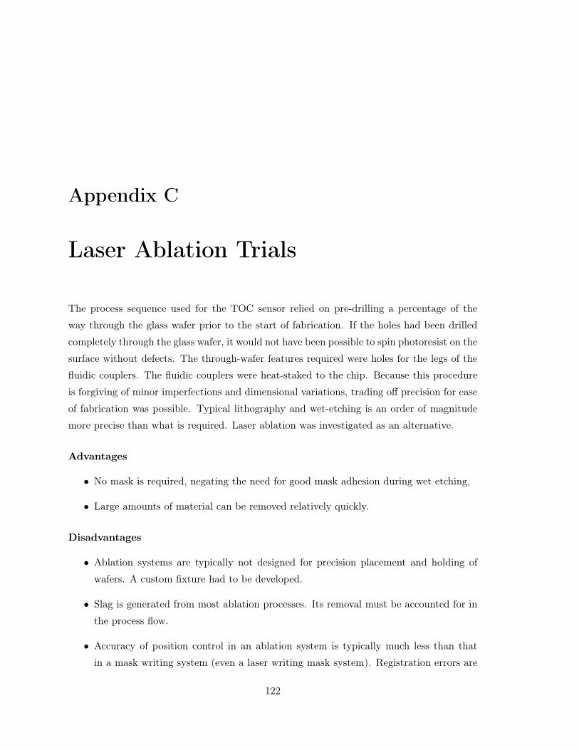
Appendix C
Laser Ablation Trials
The process sequence used for the TOC sensor relied on pre-drilling a percentage of the
way through the glass wafer prior to the start of fabrication. If the holes had been drilled
completely through the glass wafer, it would not have been possible to spin photoresist on the
surface without defects. The through-wafer features required were holes for the legs of the
fluidic couplers. The fluidic couplers were heat-staked to the chip. Because this procedure
is forgiving of minor imperfections and dimensional variations, trading off precision for ease
of fabrication was possible. Typical lithography and wet-etching is an order of magnitude
more precise than what is required. Laser ablation was investigated as an alternative.
Advantages
• No mask is required, negating the need for good mask adhesion during wet etching,
• Large amounts of material can be removed relatively quickly.
Disadvantages
• Ablation systems are typically not designed for precision placement and holding of
wafers. A custom fixture had to be developed.
• Slag is generated from most ablation processes. Its removal must be accounted for in
the process flow.
• Accuracy of position control in an ablation system is typically much less than that
in a mask writing system (even a laser writing mask system). Registration errors are
122

C.1. EXPERIMENTAL SETUP 123
common in matching lithography patterns to ablation patterns.
• Substrate damage (cracking) from the relatively violent process of ablation must be
investigated and considered in establishing limits for the speed and power.
C.1 Experimental Setup
The laser ablation system available was not specifically designed for MEMS or precision
fabrication. The M Class 30W CO2laser (Universal Laser Systems, Scottsdale, AZ) was
designed for precision engraving1. To establish the limits of the system and characterize
an optimal recipe, a matrix of conditions was run using a test pattern. The test pattern
consisted of a 300 mm diameter circle and 300 mm length/width cross. The parameters varied
were power, pulses per inch (PPI), resolution, and speed. The maximum resolution (mini-
mum size) of the spot size on the system was 75 mm using a fixed focal length of 3.8 cm. The
system was configured with a cone and air stream assist to prevent ablated material from
settling back on the optics. The substrates were 500 mm thick, double-side polished 100mm
wafers made of Pyrex® 7740 (Bullen Ultrasonics, Eaton, OH). Prior to ablation, 40 nm of
chromium was sputter deposited on the surface. This was to provide a “liftoff” layer that
would not interfere with ablation but would protect the surface from slag that would settle
back on the substrate during ablation. While chromium is typically reflective, the layer was
thin enough that it did not interfere with the initiation of ablation, yet it was thick enough
that it would protect the surrounding surface. Following ablation, the wafers were cleaned
in 10:1 sulfuric peroxide and the chromium layer removed by etching in chromium etchant
(CR-14, Cyantek Corporation, Fremont, CA)
Power was specified as a percentage of system maximum (30W) The differences between
50% and 100% power were investigated. The lower power tended towards smoother features
with less cracking, but at the expense of depth.
Speed and power together have the most influence on the depth of cut. Speed is specified
as the percentage of the system maximum of 25 cm/s.
Resolution does not refer to the spot size of the laser but to the minimum spot size
of control by the system driver, measured in dots per inch (DPI). Spot size was varied
between 75 mm (333 DPI) down to 25 mm (1000 DPI - system limitation). Because the lower
1Special thanks to Juan Santiago’s research group in the ME department at Stanford University for accessto their laser ablation system and to Gina Binnard for training.

124 APPENDIX C. LASER ABLATION TRIALS
resolution corresponds to the spot size, there is no overlapping of pulses. The effect of the
energy distribution in the beam can be seen in the corrugations that are visible in Figure C.6.
Etching to a more uniform depth requires overlapping pulses justifying the use of the highest
resolution.
Pulses per inch (PPI) refers to the number of times the laser fires per inch. Although
not directly tied to DPI, the two parameters work together to determine the quality of the
image.
C.2 Results

C.2. RESULTS 125
(a) Speed: 1%
(b) Speed: 5%
(c) Speed: 10%
(d) Speed: 25%
(e) Speed: 50%
(f) Speed: 75%
(g) Speed: 100%
Figure C.1: Power: 50%, PPI: 1000, Res: 1000

126 APPENDIX C. LASER ABLATION TRIALS
(a) Speed: 1%
(b) Speed: 5%
(c) Speed: 10%
(d) Speed: 25%
(e) Speed: 50%
(f) Speed: 75%
(g) Speed: 100%
Figure C.2: Power: 100%, PPI: 1000, Res: 1000

C.2. RESULTS 127
(a) Speed: 1% (b) Speed: 5%
(c) Speed: 10% (d) Speed: 25%
(e) Speed: 50% (f) Speed: 75%
(g) Speed: 100%
Figure C.3: Power: 100%, PPI: 500, Res: 500

128 APPENDIX C. LASER ABLATION TRIALS
(a) Speed: 1%
(b) Speed: 5%
(c) Speed: 10%
(d) Speed: 25%
(e) Speed: 50%
(f) Speed: 75%
(g) Speed: 100%
Figure C.4: Power: 100%, PPI: 333, Res: 1000

C.2. RESULTS 129
(a) Speed: 1% (b) Speed: 5%
(c) Speed: 10% (d) Speed: 25%
(e) Speed: 50% (f) Speed: 75%
(g) Speed: 100%
Figure C.5: Power: 100%, PPI: 333, Res: 500

130 APPENDIX C. LASER ABLATION TRIALS
(a) Speed: 1% (b) Speed: 5%
(c) Speed: 10% (d) Speed: 25%
(e) Speed: 50% (f) Speed: 75%
(g) Speed: 100%
Figure C.6: Power: 100%, PPI: 333, Res: 333

Appendix D
Mechanical Drawing TOC Die
Figure D.1: Mechanical Drawing of Laser Ablation Drill Pattern
131

132 APPENDIX D. MECHANICAL DRAWING TOC DIE
Figure D.2: Drill pattern for TOC die and microfluidic fuel cell.