Embed Size (px)
Citation preview
FABRICATION OF FREQUENCY SELECTIVE STRUCTURE AND
EVALUATION OF MICROWAVE TRANSMISSION ON ENERGY
SAVING GLASS
LIM HUEY SIA
A thesis submitted in
fulfilment of the requirements for the award of the
Degree of Master of Electrical Engineering with Honors
Faculty of Electrical and Electronic Engineering
Universiti Tun Hussein Onn Malaysia
FEB 2015

7
ABSTRACT
The use of energy saving glass has become very popular in the modern day building
design. This energy saving property is achieved by applying a very thin tin oxide
(SnO2) coating on one side of the glass. This coating can provide good thermal
insulation to the buildings by blocking infrared rays while being transparent to
visible part of the spectrum. Drawbacks of these energy saving windows is that it
also attenuates the transmission of useful microwave signals through them. These
signals fall within the frequency band of 0.8GHz to 2.2GHz. In order to pass these
signals through the coated glass, the use of aperture type frequency selective surface
(FSS) has being proposed. In the present work, SnO2 thin film with FSS structure
was fabricated using RF magnetron sputtering technique and printed circuit board
technology. Deposition time, dissipation power and oxygen flow rate were varied
during the sputtering deposition process. Atomic force microscopy (AFM) and field
emission-scanning electron microscopy (FE-SEM) were used to analyze the surface
morphology and roughness of the SnO2 thin film. Two point electrical probe analysis
was used to determine the sheet resistance and resistivity of the SnO2 thin film.
Thickness of SnO2 thin film was measured using surface profiler. Good correlation
between the surface properties and electrical properties of SnO2 thin film was
obtained. Microwave transmission through SnO2 coated glass with FSS structure was
also analyzed using network analyzer. The result of computer simulation was
confirmed and consistent with the network analyzer results that showed the
improvement of SnO2 coated glass with the FSS structure. Thermal analysis
demonstrated that FSS structure had allows the transmission of GSM mobile signal
penetrate in the buildings while blocking the infrared light with the SnO2 film
properties.

8
ABSTRAK
Penggunaan kaca yang boleh menjimatkan tenaga adalah sangat popular dalam
bangunan moden masa kini. Konsep kaca penjimatan tenaga boleh dihasilkan dengan
menggunakan timah oksida (SnO2) yang sangat nipis dan disalut pada satu
permukaan kaca. Lapisan ini akan menebat haba dengan baik pada bangunan-
bangunan, iaitu dengan menghalang sinaran inframerah daripada telus ke dalam
bangunan. Salah satu kelemahan salutan SnO2 ini adalah ia akan melemahkan
penghantaran isyarat yang berguna seperti gelombang telefon daripada melalui
salutan SnO2. Penggunaan struktur frekuensi terpilih (FSS) adalah dicadangkan
untuk mengatasi masalah ini. Di dalam projek ini, lapisan SnO2 dan struktur FSS
dibentuk dengan menggunakan RF magnetron sputtering dan teknologi papan litar
tercetak. Mikroskop tekanan atom (AFM) dan mikroskop imbasan elektron –
pancaran medan (FE-SEM) telah digunakan untuk menganalisis morfologi
permukaan dan kekasaran filem nipis SnO2. Two point probe digunakan untuk
menentukan rintangan filem nipis SnO2. Ketebalan filem nipis diukur menggunakan
surface profiler. Perkaitan yang baik di antara sifat-sifat permukaan dan sifat elektrik
SnO2 filem nipis telah ditemui. Ketebalan filem ini juga sangat berhubung kait
dengan sifat-sifat elektrik filem. Kadar penembusan gelombang mikro melalui
salutan SnO2 berserta struktur FSS dikaji menggunakan network analyzer. Hasil
simulasi komputer telah disahkan dan konsisten dengan hasil kajian network
analyzer yang menunjukkan peningkatan dalam penembusan gelombang melalui
kaca bersalut SnO2 dengan struktur FSS. Hasil kajian suhu juga mendapati struktur
FSS telah meningkatkan penghantaran isyarat GSM dengan menembusi dalam
bangunan manakala menyekat pemanasan inframerah.

9
CONTENTS
TITLE i
DECLARATION ii
DEDICATION iii
ACKNOWLEDGEMENT iv
ABSTRACT vi
CONTENTS viii
LIST OF FIGURES xii
LIST OF SYMBOLS AND ABBREVIATIONS xix
CHAPTER 1 INTRODUCTION 1
1.1 Background of Research 1
1.2 Problem Statement and Objective 3
1.3 Scope of Research 3
1.4 Outline of Thesis 4
CHAPTER 2 LITERATURE REVIEW 5
2.1 Energy Saving Glass 6
2.2 Thin Film Deposition 9
CHAPTER 3 RESEARCH METHOLOGY 11
3.1 Radio Frequency (RF) Magnetron
Sputtering Deposition
12
3.2 Computer Simulation Technology (CST) 15
3.2.1 Electromagnetic Simulation Workflow 16
3.3 Printed Circuit Board Technology and
Fabrication of FSS Structure
17
3.4 Thin Film Characterization 19
3.4.1 Surface Profiler and Two Point Probe

10
3.4.2 Field Emission Scanning Electron
Microscope (FESEM) and Atomic Force
Microscope (AFM)
21
3.4.3 X-Ray Diffraction (XRD) and UV-Vis 23
3.5 Spectrum Analyzer, Network Analyzer,
Glass and Thermal Properties
25
3.6 Glass Dielectric Constant Measurement 30
CHAPTER 4 ELECTROMAGNETIC SIMULATION
USING CST: FSS STRUCTURE
31
4.1 CST Simulation Using Various SnO2
Sheet Resistance Values
32
4.1.1 CST Simulation Using Conventional Sheet
Resistance
34
4.1.2 CST Simulation Using Sheet Resistance of
SnO2 Thin Film Deposited Using RF
Magnetron Sputtering System
36
4.2 CST Simulation Using Various Shape of
FSS Structure
38
CHAPTER 5 SnO2 THIN FILM ANALYSIS 45
5.1 Electrical Properties of SnO2 Thin Film
Deposited at Various Parameters
45
5.1.1 Thickness and Sheet Resistance of SnO2
Deposited at Different Deposition Time
46
5.1.2 Correlation between Thickness and Sheet
Resistance of SnO2 Thin Film
48
5.2 Physical properties of SnO2 Thin Film 48
5.2.1 Roughness analysis using AFM 49
5.2.2 FESEM Result of SnO2 Thin Film 50
5.3 Structural Composition and Optical
Properties of SnO2 Thin Film
51
5.3.1 XRD Result of SnO2 Thin Film 51
5.3.2 Optical Transmission through SnO2 Thin 52

11
Film
5.4 Thickness and Sheet Resistance of SnO2
Deposited at Different Oxygen Flow Rate
53
5.5 Physical properties of AFM Result for
SnO2 thin film
55
5.5.1 FESEM Result of SnO2 Thin Film 56
5.5.2 XRD Result of SnO2 Thin Film Deposited
at Different Oxygen Flow Rate
57
5.6 Thickness and Sheet Resistance of SnO2
Deposited at Different Dissipation Power
59
5.6.1 AFM Result of SnO2 Thin Film Deposited
at Different Dissipation Power
61
5.6.2 FESEM Result of SnO2 Thin Film
Deposited at Different Dissipation Power
62
5.7 XRD Result of SnO2 Thin Film Deposited
at Different Dissipation Power
64
CHAPTER 6 MOBILE RADIO SIGNAL TRANSMISSION
AND THERMAL PROPERTIES THROUGH
SnO2 THIN FILM DEPOSITED AT
VARIOUS PARAMETERS
66
6.1 Signal Magnitude Analysis 67
6.1.1 Signal Magnitude Analysis Result of SnO2
Film Deposited at Different Deposition
Time
68
6.1.2 Signal Magnitude Analysis Result of SnO2
Film Deposited at Different Oxygen Flow
Rate
72
6.1.3 Signal Magnitude Analysis Result of SnO2
Film Deposited at Different Dissipation
Power
77
6.2 Signal Transmission Analysis 82
6.2.1 Signal Transmission Result of SnO2 Film
Deposited At Different Deposition Time
82

12
6.2.2 Signal Transmission Result of SnO2 Film
Deposited At Different Oxygen Flow Rate
84
6.2.3 Signal Transmission Result of SnO2 Film
Deposited At Different Dissipation Power
85
6.3 Thermal Insulation Properties 87
CHAPTER 7 CONCLUSION 88
7.1 Strength of this Project 90
7.2 Future Work 90
REFERENCES 92
APPENDICES 102

13
LIST OF FIGURES
2.1 Illustration of energy saving glass with the FSS
structure.
8
3.1 Flow chart to fabricate energy saving glass 11
3.2 Tin oxide (SnO2) target material. 12
3.3 Fluorine Tin Oxide (FTO) target material. 12
3.4 Schematic diagram of magnetron source. 13
3.5 Magnetron sputtering operation system. 14
3.6 Overview of RF magnetron sputtering setup. 15
3.7 CST studio suite 2013 used for simulation. 15
3.8 Basics procedure in CST simulation. 16
3.9 Process flow of FSS formation. 17
3.10 Procedure on frequency selective structure (FSS)
printed on the glass.
18
3.11 Front illustration for the glass before and after
coating.
19
3.12 Surface profiler Alpha Step IQ. 20
3.13 Electrical properties measured using 2 point
probing.
21
3.14 Image of the FESEM (JEOL JSM-7600F)
operation system.
21
3.15 Configuration of the FESEM (JEOL JSM-7600F)
operation system.
22
3.16 Image of the Park System AFM (model XE-100)
operation system.
22
3.17 Configuration of the Park System AFM (model 23
14
XE-100) and its operation.
3.18 Glazing incidence diffraction experimental setup. 24
3.19 Picture of the Panalytical X‟Pert Pro-MRD used
for the measurement.
25
3.20 Illustration of UV-Vis spectrometry. 25
3.21 Measurement setup for spectrum analyzer. 25
3.22 Spectrum analyzer of Advantest R3132 used in
measurement.
26
3.23 Experimental setup for spectrum analysis. 26
3.24 Measurement setup for network analyzer testing. 27
3.25 Picture of Rohde&Schwarz network analyzer
(ZVB 4) used in the measurement.
27
3.26 Experimental setup for the network analyzer
testing.
28
3.27 Measurement setup for temperature measurement. 28
3.28 Experimental setup for temperature measurement. 29
3.29 IR thermometer used in temperature
measurement.
29
3.30 Agilent 4291B used for dielectric constant
measurement.
30
3.31 Glass attached to the rod for measurement. 30
4.1 Dielectric constant measured by Agilent 4291B. 31
4.2 Illustration of sheet resistance measured by the 2
point probe.
32
4.3 Microwave transmission at various ohmic sheet
resistances and without FSS structure.
32
4.4 Microwave transmission at various ohmic sheet
resistances and with FSS structure.
33
4.5 Microwave transmission at 4 ohmic sheet
resistances and with and without FSS structure.
34
4.6 Microwave transmission at 6 ohmic sheet
resistances and with and without FSS structure.
35

15
4.7 Microwave transmission at various deposition
times with the FSS structure.
36
4.8 Microwave transmission at various oxygen flow
rate with the FSS structure.
37
4.9 Microwave transmission at various dissipation
powers with the FSS structure.
37
4.10 Design of cross-dipole frequency selective surface
unit cell on energy saving glass.
39
4.11 Design of circle frequency surface unit cell on
energy saving glass.
39
4.12 Design of pentagon frequency selective surface
unit cell on energy saving glass.
39
4.13 Design of triangle frequency selective surface unit
cell on energy saving glass.
40
4.14 Design of combine structure frequency selective
surface unit cell on energy saving glass.
40
4.15 A plot demonstrating technique to measure full
width half maximum, minimum transmission loss
and peak frequency from the simulation result.
41
4.16 Transmission loss through different shapes of
frequency selective surface.
42
4.17 Effect on different shapes through FWHM and
peak frequency analysis.
42
4.18 Minimum transmission loss through different
shapes of frequency selective structure.
43
4.19 Surface area etched with the minimum
transmission loss with different shapes.
44
5.1 Thickness of SnO2 film under different deposition
time.
46
5.2 Correlation between sheet resistance and
resistivity of the SnO2 thin film under different
deposition time.
47

16
5.3 AFM image of SnO2 thin film deposited at (a) 10
minutes, (b) 20 minutes and (c) 30 minutes
deposition time.
49
5.4 FESEM image of SnO2 thin film deposited at (a)
10minutes, (b) 20minutes and (c) 30minutes.
50
5.5 XRD image of SnO2 thin film that deposited at
different deposition time.
51
5.6 Transmittance of SnO2 thin film that deposited at
different deposition time.
52
5.7 Thickness and deposition rate of SnO2 film under
different oxygen flow rate.
53
5.8 Correlation between sheet resistance and
resistivity under different oxygen flow rate.
54
5.9 AFM image of SnO2 thin film deposited at (a) 0
sccm, (b) 4sccm, (c) 8sccm and 16sccm.
55
5.10 FESEM images of SnO2 thin film deposited at (a)
0sccm, (b) 4sccm, (c) 8sccm and (d) 16sccm of
O2 flow rate. The RF power and total pressure
were 225W and 8.25mTorr, respectively.
56
5.11 XRD image of SnO2 thin film that deposited at
different oxygen flow rate.
58
5.12 Transmittance of the SnO2 thin film that deposited
at different oxygen flow rate.
58
5.13 Correlation of thickness and deposition rate of
SnO2 thin film with different dissipation power.
59
5.14 Correlation between sheet resistance and
resistivity under different dissipation power.
60
5.15 AFM image of SnO2 thin film that deposited (a)
150W, (b) 200W, (c) 225W, (d) 250W and (e)
300W.
62
5.16 FESEM images of SnO2 thin film deposited at (a)
150W, (b) 200W, (c) 225W and (d) 250W and (e)
63

17
300W of dissipation power. The deposition time
and total pressure were 20minutes and 8.25mTorr,
respectively.
5.17 XRD image of SnO2 thin film that deposited at
different dissipation power.
64
5.18 Transmittance of SnO2 thin film that deposited at
different dissipation power.
65
6.1 Mobile signal strength tested with spectrum
analyzer at (a) 0˚, (b) 15˚ (c) 30˚.
67
6.2 Signal magnitude analysis on a SnO2 thin film
with FSS structure that deposited at different
deposition time
68
6.3 Signal magnitude analysis on a SnO2 thin film
with FSS structure that deposited at different
deposition time.
69
6.4 Signal magnitude analysis at 15 degree on a SnO2
thin film that deposited at different deposition
time.
70
6.5 Signal magnitude analysis at 15 degree on a SnO2
thin film with FSS structure that deposited at
different deposition time.
70
6.6 Signal magnitude analysis at 30 degree on a SnO2
thin film that deposited at different deposition
time.
71
6.7 Signal magnitude analysis at 30 degree on a SnO2
thin film with FSS structure that deposited at
different deposition time.
72
6.8 Signal magnitude analysis on a SnO2 thin film
that deposited at different oxygen flow rate.
73
6.9 Signal magnitude analysis on a SnO2 thin film
with FSS structure that deposited at different
oxygen flow rate.
73

18
6.10 Signal magnitude analysis at 15 degree on a SnO2
thin film that deposited at different oxygen flow
rate.
74
6.11 Signal magnitude analysis at 15 degree on a SnO2
thin film with FSS structure that deposited at
different oxygen flow rate.
75
6.12 Signal magnitude analysis at 30 degree on a SnO2
thin film that deposited at different oxygen flow
rate.
76
6.13 Signal magnitude analysis at 30 degree on a SnO2
thin film with FSS structure that deposited at
different oxygen flow rate.
76
6.14 Signal magnitude analysis on a SnO2 thin film
that deposited at different dissipation power.
77
6.15 Signal magnitude analysis on a SnO2 thin film
with the FSS structure that deposited at different
dissipation power.
78
6.16 Signal magnitude analysis at 15 degree on a SnO2
thin film that deposited at different dissipation
power.
79
6.17 Signal magnitude analysis at 15 degree on a SnO2
thin film with the FSS structure that deposited at
different dissipation power.
79
6.18 Signal magnitude analysis at 30 degree on a SnO2
thin film that deposited at different dissipation
power.
80
6.19 Signal magnitude analysis at 30 degree on a SnO2
thin film with the FSS structure that deposited at
different dissipation power.
81
6.20 Signal transmission testing on a SnO2 thin film
that deposited at different deposition time.
82
6.21 Signal transmission testing on a SnO2 thin film 83

19
with the FSS structure that deposited at different
deposition time.
6.22 Signal transmission testing on a SnO2 thin film
that deposited at different oxygen flow rate.
84
6.23 Signal transmission testing on a SnO2 thin film
with the FSS structure that deposited at different
oxygen flow rate.
85
6.24 Signal transmission testing on a SnO2 thin film
that deposited at different dissipation power.
86
6.25 Signal transmission testing on a SnO2 thin film
with the FSS structure that deposited at different
dissipation power.
86
6.26 Measured temperature for different samples of
glass.
87
20
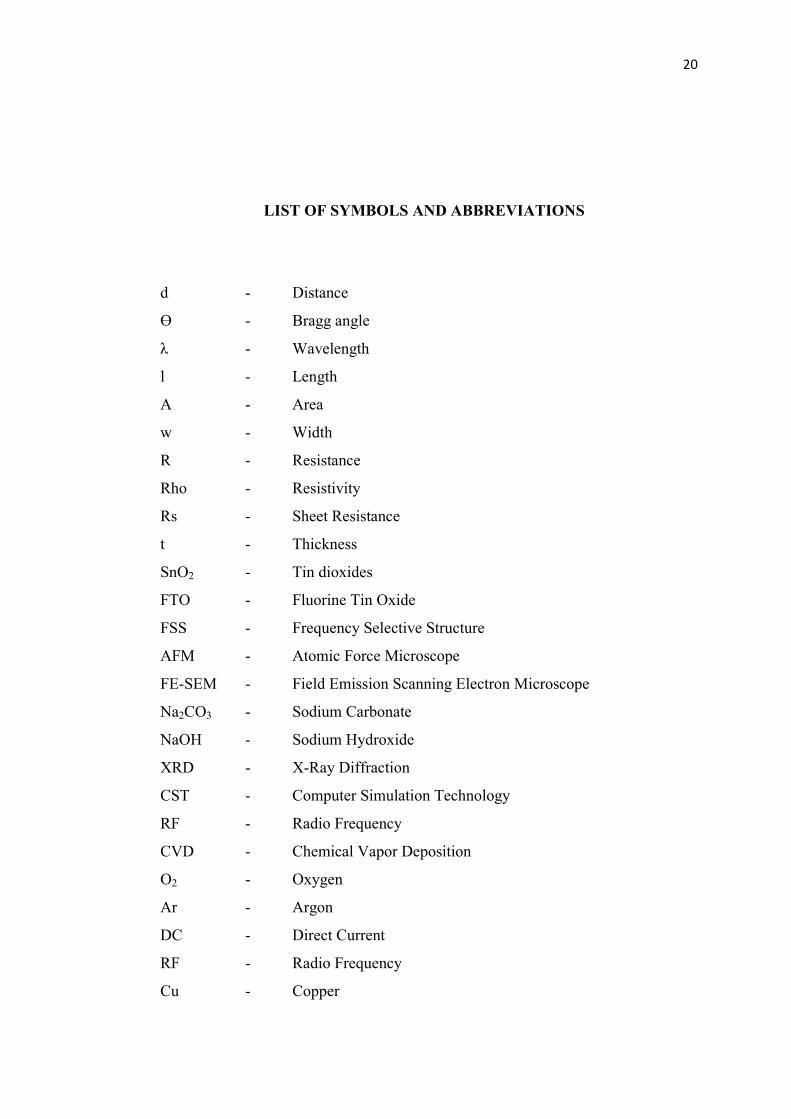
LIST OF SYMBOLS AND ABBREVIATIONS
d - Distance
Ɵ - Bragg angle
λ - Wavelength
l - Length
A - Area
w - Width
R - Resistance
Rho - Resistivity
Rs - Sheet Resistance
t - Thickness
SnO2 - Tin dioxides
FTO - Fluorine Tin Oxide
FSS - Frequency Selective Structure
AFM - Atomic Force Microscope
FE-SEM - Field Emission Scanning Electron Microscope
Na2CO3 - Sodium Carbonate
NaOH - Sodium Hydroxide
XRD - X-Ray Diffraction
CST - Computer Simulation Technology
RF - Radio Frequency
CVD - Chemical Vapor Deposition
O2 - Oxygen
Ar - Argon
DC - Direct Current
RF - Radio Frequency
Cu - Copper

21
PSPD - Position-Sensitive Photo Detector
Au - Gold
2D - Two Dimensional
3D - Three Dimensional

22
CHAPTER 1
INTRODUCTION
1.1 Background of Research
Malaysia is a tropical country with hot and wet weather all along the years [1]. With
the weather of 34˚C in average, air conditioning is basic equipment in modern
buildings to release the heats to outside [2]. Thus, electrical power consumption
increases with the air conditioning usage in the buildings. In addition, heavy usage of
air conditioning is not good for the mother earth due to depleting of ozone layer [2].
Recently, energy saving glass has been developed to overcome this problem [3–12].
Energy saving glass could help to reduce the temperature inside the buildings by
reflecting the infrared light that penetrates through the building.
The most basic energy saving glass is a glass that applied with a very thin tin
oxide (SnO2) film on it. This SnO2 material is a semiconducting oxide that have
higher band gap that are suitable in the gas sensors [13–17] due to the higher free
electrons in the oxygen vacant holes and thus increased the electrical conductivity of
the thin film, solar cells [18], flat panels display [19] and photo catalysis [20].
However, the disadvantage of the energy saving glass is that it reflects the important
electromagnetic wave such as GSM mobile signal, GPS and Bluetooth. In order to
improve the electromagnetic signal inside the building, FSS had been added into the
energy saving glass [6], [8], [21–24]. This FSS structure helps to enhance the
electromagnetic wave inside the building. Different FSS structure will give different
transmission at various frequencies. The optimized FSS structure will give the better
transmission in the particular frequency.

23
FSS is a structure that allow the certain frequencies to passed through it while
block other frequencies. The used of FSS in this project was to improve the
microwave frequencies. In the past few years, many researchers had tried to apply
different structure on the energy saving glass [6], [21–25]. Bandpass FSS that act as
filter with single, double and triple glass used to improve the transmission of
RF/microwave frequencies. The sheet resistance of the film plays a vital role in the
improvement of the energy saving glass with the FSS structure. From Liu et al
findings, decreased in sheet resistance will increase the shielding effect of the
electromagnetics wave [26]. The material of the metal oxide had the effects towards
the sheet resistance of the film. The transmission of the electromagnetic wave affects
once the sheet resistance changed.
Besides that, most of the researchers were using the Pilkington energy saving
glass to form the FSS structure on it with the laser technique [27]. In this thesis,
fabrication of energy saving glass with FSS structure will be presented. The
fundamental properties of coated SnO2 thin film and its testing toward FSS
applications will be discussed. These testing and analyses are needed for optimum
usage of energy saving glass application at the modern design building.
Fluorine doped tin oxide (FTO) is the common material used for the energy
saving glass that fabricated by Pilkington United Kingdom (UK) [28]. The technique
used by Pilkington was chemical vapor deposition (CVD) technique. However, FTO
material is not an environmental friendly material due to fluorine gas process which
is a toxic gas. Thin film fabrication under CVD technique will require high
temperature which needs more time in production.
Indium tin oxide (ITO) also been found in the microwave frequency
application [29]. But, the ITO is an expensive material that will results in high
production cost. In the present research, magnetron sputtering process will be used to
fabricate SnO2 thin film. The deposition was done in room temperature which had
reduced the processing time and then lead to cost saving effect. Besides that, the
energy saving glass available for four season country is double panels that argon gas
was filled in the middle of it [6], [9], [12], [21], [28], [30] and currently none of the
research was reported in Malaysia. This energy saving glass is specially designed for
four season countries. While Malaysia is a tropical country that only needs a single
panel of energy saving glass [31]. For single panel energy saving glass is relatively

24
cheaper than the double panel energy saving glass that filled with Argon gas. SnO2
was used as the material for energy saving glass due to its high reflectivity towards
the infrared light (IR) [32–34]. Besides that, SnO2 thin film is also chemically stable
that can stay long lasting [35–37].
1.2 Problem Statement and Objective
Nowadays, energy saving glass can keep the room cold at the summer and warm at
the winter. But at the same time it attenuates the useful microwave frequencies such
as GSM mobile signal. Because of this, a FSS structure needs to be added into
energy saving glass to improve the transmission of the energy saving glass. Different
design of FSS can have different of transmission on the glass. The transmission loss
also been influenced by the sheet resistance of the film.
The objectives of this project are to:
1. To simulate the transmission of the microwave signal through energy saving
glass with different structure of FSS.
2. To experimentally deposit tin oxide (SnO2) on glass substrate using RF
magnetron sputtering technique and evaluate its characteristics.
3. To evaluate the heat reduction, mobile radio signal transmission through the
SnO2 glass with FSS structure and without FSS structure fabricated by RF
magnetron sputtering.
1.3 Scope of Research
In order to meet above objectives, this project is carried out according to below:
1. Computer simulation using CST software for different FSS structure in
microwave frequencies.
2. Fabrication of FSS structure using printed circuit board technology.
3. Deposition of SnO2 thin film using RF magnetron sputtering plasma.
4. Surface morphology, optical and electrical properties of SnO2 thin film
analyses.
5. Microwave transmission analysis in the frequency range of 0.8-2.2GHz
through SnO2 coated glass with FSS structures.

25
1.4 Outline of Thesis
This thesis is consists of 7 chapters. The first chapter describes an overview of this
project. The second chapter explains the literature review of previous works and
techniques used in this project. The third chapter presents the experimental setup and
equipment used for analyses. The fourth chapter explains the SnO2 thin film analysis
on electrical, physical and optical properties. The fifth chapter describes the CST
simulation with different FSS structures and sheet resistance obtains from the
electrical properties of the SnO2 film. The sixth chapter presents the microwave
transmission analysis tested with spectrum and network analyzers. Finally, the last
chapter described conclusion of the findings throughout the project and propose
future work.

CHAPTER 2
LITERATURE REVIEW
Energy saving glass was widely applied in the buildings nowadays. This energy
saving glass used to save the power consumption and the mother earth [38]. Malaysia
is a tropical country which is hot and wet weather, throughout the year. Energy
saving glass was applied a transparent metallic oxide layer on it. The metal oxide has
the ability to reflect the electromagnetic radiation from penetrates into the buildings.
But this metallic oxide layer also attenuates the useful signal such as GSM mobile
radio signal. In order to improve the electromagnetic wave such as GSM mobile
radio signal, a FSS was introduced. The main reason of applying FSS glass was to
eliminate the electromagnetic radiation of infrared as much as possible and then the
electromagnetic wave of GSM mobile radio signal can be passing through.
Energy saving glass had been widely explored by many researchers to obtain
better transmission in microwave frequency range in the past few years [5], [9], [27],
[39]. For example, Irfan et al had successfully design an energy saving glass with
dual bandpass FSS by hard coating technique [23]. From his findings, the FSS
structure able to attenuates 92.7% IR radiation. While Syed et al had reported that
combination of low pass and high pass FSS glass had 30dB transmission
improvement in the microwave frequency range [6]. Besides that, Mats et al reported
that the transmission improvement of 10dB had been achieved with FSS window
[12]. Then, Rafique et al had successfully designed a dual band circular loop FSS
with the improvement in transmission of 26.4dB [24]. Last but not least, Ghaffer et
al had reported that cross dipole FSS had transmission improvement in the
microwave frequency range of 11.3dB [27].

27
FSS had broadly used in many other applications such as antenna, building
and transportation. From the findings, Philippakis et al had reported that FSS
structure can applied on the wallpaper for better transmission [21]. Besides that,
Russo et al had successfully design FSS structure on the application of beam steering
[40]. Then, Ragan et al had reported that FSS structure in millimeter wave integrated
circuits application [41]. The application of FSS in millimeter astronomy had
reported by Ge et al [42]. Lastly, Lee et al had reported that FSS structure can
improve the WLAN application in his findings [43].
2.1 Energy Saving Glass
Energy saving glass had widely been developed in the past few years. The energy
saving glass applied in the country which has four seasons is good that could
maintain the temperature in winter or summer. But in Malaysia, energy saving glass
can helps to reduce the high temperature inside the buildings even though Malaysia
do not have four season. With the energy saving glass applied on the buildings will
help to save a lot of the electricity bill for long term usage.
Energy saving glass is divided into two types, which are tinted film and thin
film. Tinted film is well known in the market today that have the properties to reflect
heats and infrared light in the automotive application. In the tinted film category,
there are few types that consist of percentage of visible light and infrared
transmission.
The thin film deposited on the glass with any material can defined as thin
film that thickness of the film was ranging in nanometer. The differences of tinted
film and thin film are on the visibility of the glass and features on it. One can feel
with hand for tinted film but not for thin film. In this project, RF magnetron
sputtering technique was chosen for the thin film deposition. RF sputtering is a
technique that has high deposition rate, good reproducibility and good adhesion [44–
46]. Kim et al had done his project with investigate electrical properties of SnO2 film
deposited by RF magnetron sputtering [44]. In his research, low resistivity and high
mobility was found in SnO2 thin film for gas sensor application. Shinzo et al
reported that SnO2 film prepared by DC magnetron sputtering applied on
optoelectronics devices [45]. In the research, lowest resistivity was established at low

28
temperature in organic film substrates. Dan et al had deposited SnO2 by RF
magnetron sputtering for solar cells application [46]. In his project, oxygen partial
pressures were investigated towards the resistivity of the SnO2 film as the buffet
layer of the solar cells. The findings obtain from this project was when increased the
oxygen partial pressure, the resistivity of the film decreased.
Tin oxide thin film had been deposited by RF magnetron sputtering. SnO2
film is a transparent conducting oxides that usually found in the gas sensor and solar
cells application [14], [16], [18], [47–48]. From Selin et al findings, amorphous films
has the water permeation resistance [49]. For the window in the buildings, the water
resistance ability is very important to ensure that the SnO2 film towards the heat
insulation properties is maintained. Besides that, SnO2 film also chemically stable,
low resistivity and high optical transmittance that is suitable for energy saving glass
applications [36], [50].
FSS is an aperture that only allows certain of frequency band to pass through
it [51–52]. Different FSS structure will brings different effects on the transmission
along the frequencies range. FSS structure can be added in wallpaper [21], [53] and
antenna application other than energy saving glass application [8], [22–24], [30],
[33], [40–42], [54–72]. FSS structure added will help to improve the electromagnetic
wave such as GSM mobile signal, wireless network, GPS and bluetooth signal in the
certain area [43]. The interest of frequency range in this thesis is the microwave
frequencies which range between 0.8GHz to 2.2GHz.
The concept of FSS has a long history of development over years. Several
applications of FSS can be applied on marketable things and military sectors to
enable multiple frequency band operation. For an example, FSS concept had been
applied in microwave oven which reflects at 2.45GHz microwave energies but
allowing light to pass through it [73].
CST is a tool that used to simulate the FSS structure on the glass towards the
transmission in the frequency range of 0.8GHz to 6GHz. It helps to analyze the
transmission from the transmitter to receiver with different design and different sheet
resistance to figure out the most suitable parameter or material to be used in the
energy saving glass application. It will save time and cost with the pre simulation
before the experimental deposition. But all the simulation in this tool is taking
perfect situation that without any losses.

29
In the CST simulation, several shape of the FSS had been simulated and
analyzed for better transmission of the electromagnetic wave that focus on 900MHz
which is GSM mobile radio signal. The selected structure was analyzed by
transmission loss, bandwidth and the center frequency of the transmission in the
microwave range.
Figure 2.1: Illustration of energy saving glass with the FSS structure.
Figure 2.1 shows the energy saving glass that coated with SnO2 film that FSS
structure had been added in it. The FSS structure is specially designed to bypass the
GSM mobile signals that pass through the buildings. In the energy saving glass
fabrication is divided into two which are hard coating and soft coating. Hard coating
means that the glass been manufactured at high temperature near 1000˚C that
material of energy saving glass was added in the coating process. This hard coating
glass can be directly applied to buildings as window once it had been done. While for
the soft coating, the coating process is separated from bare glass process. The coating
was done on the surface of the bare glass. The difference between the hard coating
and soft coating is the FSS structure can be formed in soft coating and not in the hard
coating. Both hard and soft coating can produced energy saving glass. In this project,
the aims are to investigate property of SnO2 film with FSS in energy saving glass
application. In this thesis, soft coating process was used with magnetron sputtering
technique to fabricate the energy saving glass. In soft coating process, various
parameters can be studied to characterize the optimum SnO2 thin film for energy
saving glass application. Hard coating means that the material is embedded in the
glass when the manufacturing of the glass. While for the soft coating, it is the off-line
process with the glass manufacturing. Various parameters can be changed for soft
FSS
Tin Oxide Coating
FSS
FSS
FSS

30
coating process such as layer of the coating, material, deposition time to study the
properties of the glass to suit the energy saving glass or other applications.
In this project, PCB technique was used to deposit FSS structure on glass.
Besides that, PCB technique is widely seen in fabricating electronic devices. This
PCB technique was the cheapest and fastest way in fabrication. This same technique
was applied on this project with copper sheet changed to glass substrate. With that,
the production cost of the energy saving glass will be cut down.
2.2 Thin Film Deposition
SnO2 material is a tetragonal n-type semiconductor having high band gap energy
(≈3.6eV) [74]. Tin oxide thin film has been reported for various applications mostly
on optics, solar, transistor and gas sensor [16], [75–78]. Chemical vapor Deposition
(CVD), sol-gel, electrode deposition and magnetron sputtering techniques are
familiar as deposition technique used for thin film deposition. In this project,
magnetron sputtering technique has been chosen due to its highly reproducible,
chemically stable and high deposition rate [44], [79]. In addition, the deposition
occurs at room temperature condition which is much cheaper in cost. In general,
there are two sources power in magnetron sputtering technique which is Radio
Frequency (RF) and Direct Current (DC). Radio frequency source is suitable for
most of the target material while direct current source is more suitable for metal
target material. In this project, SnO2 was chosen as target material thus RF source
power supply was chosen for magnetron sputtering deposition. Tin oxide is a fragile
material, therefore the copper backing plate is required on tin oxide target. In this
project, RF source power supply was chosen instead of DC source power supply was
because of tin oxide is a breakable material that is not suitable for to apply DC
source power supply. In RF source power supply, the power will go to auto matching
box before reach the target material. While the DC source power supply, the power
will directly go to target material without any auto matching box. The purpose of
auto matching box was to control the power supply source constantly in the process
of deposition.
From this chapter, the energy saving glass properties was studied. Soft
coating method was selected because FSS structure can be formed on it. RF

31
magnetron sputtering technique was chosen for the SnO2 thin film deposition. The
CST simulation, FSS forming process and thin film characterization will be
discussed in next chapter.

CHAPTER 3
RESEARCH METHODOLOGY
As mentioned in previous chapter, SnO2 thin film was prepared using magnetron
sputtering machine. Several analyses were carried out such as surface profiler,
FESEM and AFM. The analysis is required to find the suitable parameter to fabricate
an energy saving glass that can reflect most of the infrared while maintains good
GSM signals. Besides that, sheet resistance of the thin film also takes into account to
simulate the transmission along the GSM mobile signals. Different sheet resistance
will brings effect to the transmission of microwave frequencies.
Figure 3.1: Flow chart to fabricate energy saving glass.
CST simulation with various parameter such as changing sheet resistance and
shape of FSS
Printed circuit board technique used to fabricate FSS structure
Fabricate the SnO2 thin film using magnetron sputtering technique under
various parameters
Analysis of thin film fabricated
FESEM – Surface
topography, AFM – Surface
roughness and grain size,
Surface profiler – Thickness,
2 point probe – Sheet
resistance and resistivity Spectrum and network
analyzer testing for GSM and
microwave frequencies testing
Energy saving glass that can reflect infrared
and have good GSM signal purposes
Deposited on 10 cm glass for testing
purposes
33
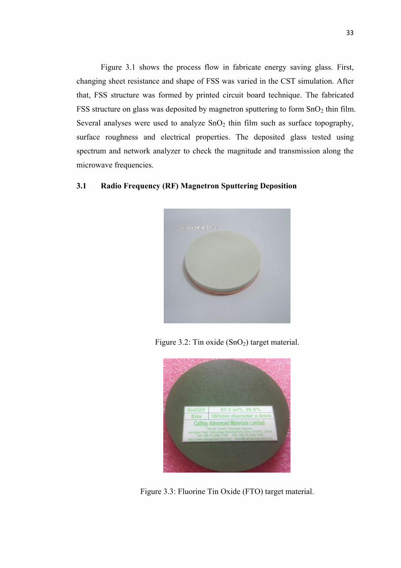
Figure 3.1 shows the process flow in fabricate energy saving glass. First,
changing sheet resistance and shape of FSS was varied in the CST simulation. After
that, FSS structure was formed by printed circuit board technique. The fabricated
FSS structure on glass was deposited by magnetron sputtering to form SnO2 thin film.
Several analyses were used to analyze SnO2 thin film such as surface topography,
surface roughness and electrical properties. The deposited glass tested using
spectrum and network analyzer to check the magnitude and transmission along the
microwave frequencies.
3.1 Radio Frequency (RF) Magnetron Sputtering Deposition
Figure 3.2: Tin oxide (SnO2) target material.
Figure 3.3: Fluorine Tin Oxide (FTO) target material.

34
Figure 3.2 shows the SnO2 target material that used for magnetron sputtering
deposition. This target had 3” diameter in size with thickness of 0.5” and the color of
the target is nearly white. The copper backing is needed for the compound and fragile
material. Figure 3.3 displays the FTO target that used for deposition process. The
color of the FTO target was seen darker than SnO2 target. For the FTO material, the
coating on the glass will be less transparent than SnO2 film. For the windows
application in the buildings, transparency of the glass is a very important.
In sputtering process, a target is bombarded by energetic ions generated in
glow discharge plasma. The bombardment process caused the removal of target
atoms, which condense on a substrate as a thin film. Besides that, ion bombardment
process also produced secondary electrons from the target surface. This secondary
electron plays an important role in maintaining the plasma. Magnetrons are the
concept of magnetic field configured parallel to the target surface can constrain
secondary electron motion to the vicinity of the target. In the magnetron sputtering
deposition, various parameters can be varied such as substrates bias voltage,
substrate temperature, dissipation power, oxygen flow rate, deposition time and
working pressure of the chamber. Vary parameters can be affects towards the film
properties [46], [80–81].
Figure 3.4: Schematic diagram of magnetron source [82].
Cooling water
Insulator
Yoke
Permanent
magnet
SnO2 target ф 75mm
(Cathode)
Ground Shield
(Anode)
Magnetic Field
35
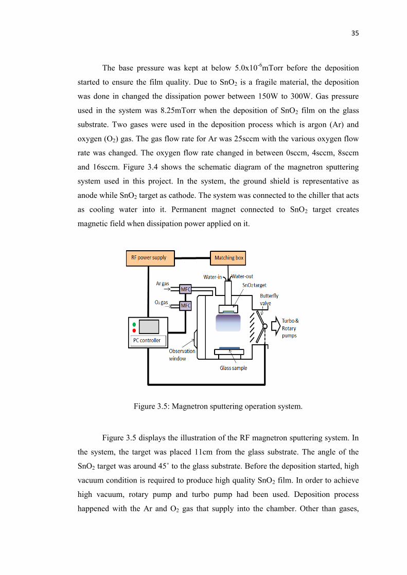
The base pressure was kept at below 5.0x10⁻⁶
mTorr before the deposition
started to ensure the film quality. Due to SnO2 is a fragile material, the deposition
was done in changed the dissipation power between 150W to 300W. Gas pressure
used in the system was 8.25mTorr when the deposition of SnO2 film on the glass
substrate. Two gases were used in the deposition process which is argon (Ar) and
oxygen (O2) gas. The gas flow rate for Ar was 25sccm with the various oxygen flow
rate was changed. The oxygen flow rate changed in between 0sccm, 4sccm, 8sccm
and 16sccm. Figure 3.4 shows the schematic diagram of the magnetron sputtering
system used in this project. In the system, the ground shield is representative as
anode while SnO2 target as cathode. The system was connected to the chiller that acts
as cooling water into it. Permanent magnet connected to SnO2 target creates
magnetic field when dissipation power applied on it.
Figure 3.5: Magnetron sputtering operation system.
Figure 3.5 displays the illustration of the RF magnetron sputtering system. In
the system, the target was placed 11cm from the glass substrate. The angle of the
SnO2 target was around 45˚ to the glass substrate. Before the deposition started, high
vacuum condition is required to produce high quality SnO2 film. In order to achieve
high vacuum, rotary pump and turbo pump had been used. Deposition process
happened with the Ar and O2 gas that supply into the chamber. Other than gases,

36
dissipation power and gas pressure also need to be set before the deposition process
start.
Figure 3.6: Overview of RF magnetron sputtering setup.
Ion bombardment influenced the films produced on the substrate by structure
and electrical properties. Besides that, the energy of the bombardment ions can be
increased by increasing the negative bias applied to the substrate. However, when the
negative bias increased it can bring defects in the film and decreased the overall film
properties [83]. Figure 3.6 shows the RF and DC sputtering system that available at
MiNT-SRC UTHM.
3.2 Computer Simulation Technology (CST)
Figure 3.7: CST studio suite 2013 used for simulation.

37
Computer Simulation Technology (CST) simulation is 3D electromagnetic
simulation software that can design and optimize the operating devices in a wide
range of frequencies. Frequency domain solver was chosen over transient domain
solver due to it is suitable for periodic structures application such as FSS. Besides
that, CST microwave studio features a special periodic boundary implementation that
creates for unit cells shaped. Floquet mode port was used in the port mode that
produces higher accuracy and fast simulation to ease the polarization analysis and
mode type. CST simulation was used Finite Integration Technique (FIT) that can
simulate two materials together as metal oxide layer that stack above the glass that
used in this project. In this project, CST simulation was used due to the mesh size
required was two mesh. Figure 3.7 shows the CST studio suite 2013 used in
simulation for this project. In the CST simulation, there are two solver to solve the
problems, transient and frequency simulation. Transient solver is used in order to
obtain accurate broadband results in the frequency domain where the electromagnetic
energy in the computational domain needs to be sufficiently decayed. Basically,
transient solver is use to solve electrically medium and large sized problems. It is
suitable for broadband analysis.
The steady state behavior of a model simulated using frequency domain
simulation is calculated at different frequency points. It is suitable to run the
simulation in narrow band or single frequency. This frequency domain is normally
applied on electrically small or medium sized problems. Frequency domain is
simulating in periodic structures with Floquet port modes. The step by step in CST
simulation part was in Appendix A.
3.2.1 Electromagnetic Simulation Workflow
Figure 3.8: Basics procedure in CST simulation.
Virtual prototype – model of device
under test
Choose the frequency domain
solver to run the simulation
Analysis of results
Set the solver settings of boundary conditions,
frequency range and discretization

38
Figure 3.8 shows the basic procedure in running the CST simulation. In the CST
simulation, the transmission of the signal between transmitter and receiver can be
obtained in perfect condition without any loss.
3.3 Printed Circuit Board Technology and Fabrication of FSS Structures
Figure 3.9: Process flow of the FSS formation.

39
Printed circuit board (PCB) technique was chosen in this project due to its simplicity
and low cost in fabricating the FSS structure. Besides that, this technology can easily
found in the electronic labs that ease for the experiment. The advantage of the PCB
technique compare to the laser technique was the process of fabrication. The PCB
fabrication process was easier than laser fabrication process due to the laser etching
required CO2 gas.
Figure 3.10: Procedure on frequency selective structure (FSS) printed on the glass.
Regarding the fabrication accuracy, there were around 80% successfully with
handling every process carefully. For laminating part, bubbles were not allowed on
the glass. Time control in the UV expose was one of the key points for the
fabrication process. Glass with the FSS structure developed need to be under the sun
heating for strengthens the attraction force. After that, fabrication process was done
Draw and print the structure
Tin oxide coating using magnetron sputtering technique
Laminated glass under UV exposes
Develop the structure using sodium carbonate (Na2CO3) chemical to clear the
unexposed area
Laminating the glass
Sodium hydroxide (NaOH) used to remove the film
Tin oxide coating with FSS structure
40
in high vacuum condition to avoid contamination of film. For the etching film, the
film will not been degrade as the RF deposition technique had the strong adhesion as
other deposition technique. The repeatability of the PCB fabrication process was
quite high around 95%. The difference process on this experiment is usually copper
or aluminum board will be used in etching purposes to form the structure on it and
this project is using glass to replace it. Glass is using due to the energy saving glass
application in this project. Figure 3.10 shows the process flow chart of the FSS
fabrication on the glass substrate and can best describe the FSS fabrication on the
glass.
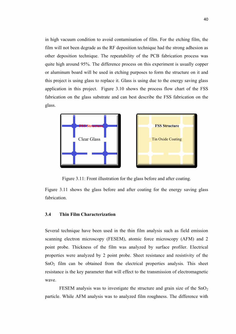
Figure 3.11: Front illustration for the glass before and after coating.
Figure 3.11 shows the glass before and after coating for the energy saving glass
fabrication.
3.4 Thin Film Characterization
Several technique have been used in the thin film analysis such as field emission
scanning electron microscopy (FESEM), atomic force microscopy (AFM) and 2
point probe. Thickness of the film was analyzed by surface profiler. Electrical
properties were analyzed by 2 point probe. Sheet resistance and resistivity of the
SnO2 film can be obtained from the electrical properties analysis. This sheet
resistance is the key parameter that will effect to the transmission of electromagnetic
wave.
FESEM analysis was to investigate the structure and grain size of the SnO2
particle. While AFM analysis was to analyzed film roughness. The difference with
Clear Glass
FSS Structure FSS Structure
Tin Oxide Coating
41
the FESEM and AFM is 2D and 3D images obtained. Transparency of the glass is
very important for the window application in the buildings. UV-Vis is a tool that
used for the glass transparency measurement. Physical composition of the SnO2 film
was analyzed by X-Ray Diffraction (XRD) technique. This analysis was to determine
the changes state of the SnO2 film with various parameters. All the analyses about
will be relate to the result of the thermal insulation properties and the transmission of
the electromagnetic wave. Details of this equipment will be discussed in research
methodology.
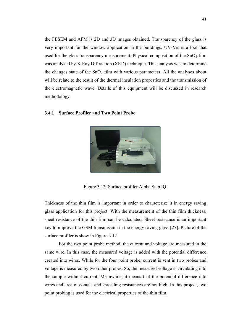
3.4.1 Surface Profiler and Two Point Probe
Figure 3.12: Surface profiler Alpha Step IQ.
Thickness of the thin film is important in order to characterize it in energy saving
glass application for this project. With the measurement of the thin film thickness,
sheet resistance of the thin film can be calculated. Sheet resistance is an important
key to improve the GSM transmission in the energy saving glass [27]. Picture of the
surface profiler is show in Figure 3.12.
For the two point probe method, the current and voltage are measured in the
same wire. In this case, the measured voltage is added with the potential difference
created into wires. While for the four point probe, current is sent in two probes and
voltage is measured by two other probes. So, the measured voltage is circulating into
the sample without current. Meanwhile, it means that the potential difference into
wires and area of contact and spreading resistances are not high. In this project, two
point probing is used for the electrical properties of the thin film.

42
Figure 3.13: Electrical properties measured using 2 point probing.
Figure 3.13 shows the two point probing that used to measure electrical
properties of the thin film. From the IV graph obtained from the two point probing,
resistivity can be calculated by Equation 3.1. Sheet resistance of the film can be
calculated by Equation 3.2 with the resistivity obtained from Equation 3.1. Besides
than the thickness and the sheet resistance of the film, dielectric constant of the glass
also take into the account when the CST simulation.
= (
) x (
) (3. 1)
(3. 2)
3.4.2 Field Emission Scanning Electron Microscope (FESEM) and Atomic
Force Microscope (AFM)
Figure 3.14: Image of the FESEM (JEOL JSM-7600F) operation system.

43
Figure 3.15: Configuration of the FESEM (JEOL JSM-7600F) operation system [84].
FESEM is a microscope that operates with electrons to form the morphology image
for the surface object [84]. Dry sample is required to achieve high vacuum condition
in scanning process. This system has two electrons operated which are primary and
secondary electrons. Primary electrons can be achieved at high vacuum condition
and then been focused and deflected to scanning unit to produce a narrow beam that
will have bombardment on the object [84]. Surface structure of the thin film is
affected by angle and velocity of the secondary electron. Electron detector detects the
secondary electron and sent the information to scanning unit. Morphology of the thin
film can be seen in computer screen after digital signal processing process the data in
the scanning unit. The operation system of the FESEM analysis is clearly showed in
Figure 3.14 and 3.15.
Figure 3.16: Image of the Park System AFM (model XE-100) operation system.
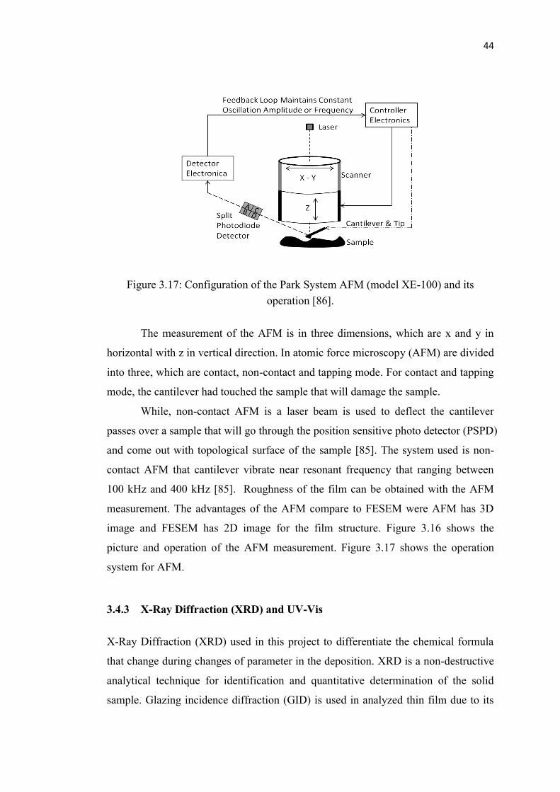
44
Figure 3.17: Configuration of the Park System AFM (model XE-100) and its
operation [86].
The measurement of the AFM is in three dimensions, which are x and y in
horizontal with z in vertical direction. In atomic force microscopy (AFM) are divided
into three, which are contact, non-contact and tapping mode. For contact and tapping
mode, the cantilever had touched the sample that will damage the sample.
While, non-contact AFM is a laser beam is used to deflect the cantilever
passes over a sample that will go through the position sensitive photo detector (PSPD)
and come out with topological surface of the sample [85]. The system used is non-
contact AFM that cantilever vibrate near resonant frequency that ranging between
100 kHz and 400 kHz [85]. Roughness of the film can be obtained with the AFM
measurement. The advantages of the AFM compare to FESEM were AFM has 3D
image and FESEM has 2D image for the film structure. Figure 3.16 shows the
picture and operation of the AFM measurement. Figure 3.17 shows the operation
system for AFM.
3.4.3 X-Ray Diffraction (XRD) and UV-Vis
X-Ray Diffraction (XRD) used in this project to differentiate the chemical formula
that change during changes of parameter in the deposition. XRD is a non-destructive
analytical technique for identification and quantitative determination of the solid
sample. Glazing incidence diffraction (GID) is used in analyzed thin film due to its

45
small diffracting volumes that caused low diffracted intensities [86]. When analyzing
thin film, parallel beam geometry is combined with glazing incidence angle to obtain
the spectrum peaks. The detector is rotates through the angular range while others is
remain constant in the collecting of the spectrum diffraction [86]. The XRD analysis
was best described by Bragg‟s Law as Equation 3.3.
(3.3)
Where n represents integer, symbolize the wavelength of the incident X-ray beam,
d is the distance between the atomic layers in crystal and is the incident angle of
the X-ray beam.
Figure 3.18: Glazing incidence diffraction experimental setup [86].
Figure 3.19: Picture of the Panalytical X‟Pert Pro-MRD used for the measurement.
113
REFERENCES
1. 2014. A Global Review. Irrigation & Drainage in the World. Retrieved Dec
14, 2014, from http://www.icid.org/i_d_malaysia.pdf
2. R. Heede. (2013). Tracing anthropogenic carbon dioxide and methane
emissions to fossil fuel and cement producers, 1854–2010. Clim. Change,
122(1-2), pp. 229–241.
3. S. H. Sohail, G. I. Kiani, and K. P. Esselle. (2011). Parametric Analysis of RF
and Microwave Transmission through Single and Multiple Layer of Float
Glass. Proceeding Asia-Pacific Microw. Converence, 2, pp. 1454–1457.
4. A. Z. Khan. (1966). Electrical energy conservation and its application to a
sheet glass industry. IEEE Trans. energy Convers., 11(3), pp. 666–671.
5. G. I. Kiani, L. G. Olsson, A. Karlsson, and K. P. Esselle. (2010) Transmission
of infrared and visible wavelengths through energy-saving glass due to etching
of frequency-selective surfaces. IET Microwaves, Antennas Propag., 4(7), pp.
955-961.
6. G. I. Kiani, A. R. Weily and K. P. Esselle. (2006). A novel absorb/transmit
FSS for secure indoor wireless networks with reduced multipath fading. IEEE
Microwave Wireless Components Letter, 16(6), pp. 378–380.
7. Q. H. Li, A. H. Meng and Y. G. Zhang. (2009). Recovery Status and Prospect
of Low-grade Waste Energy in China. Sustainable Power Generation and
Supply, pp. 1–6.

114
8. S. I. Sohail, K. P. Esselle and G. Kiani. (2012). Design of a Bandpass FSS on
Dual Layer Energy Saving Glass for Improved RF Communication in Modern
Buildings. Antennas and Propagation Society International Symposium, pp.
1–2.
9. I. Ullah, D. Habibi and G. Kiani. (2011). Design of RF/Microwave efficient
buildings using frequency selective surface. 2011 IEEE 22nd Int. Symp. Pers.
Indoor Mobile Radio Communication, pp. 2070–2074.
10. N. Yamauchi, T. Itoh and T. Noguchi. (2012). Low energy-cost TFT
technologies using ultra thin flexible glass substrate. 19th International
Workshop on Active-Matrix Flatpanel Displays and Devices, pp. 213–214.
11. C. Yang, D. Yuan, and Y. Jia. (2012). Research on energy of an office
building equipped high permeability with Low-E window in Xinxiang. 2012
2nd International Conference Consumer Electronics Commununication
Networks, pp. 508–511.
12. M. Gustafsson, A. Karlsson, A. P. P. Rebelo, and B. Widenberg. (2006).
Design of Frequency Selective Windows for Improved Indoor Outdoor
Communication. IEEE Transaction Antennas Propagation, 54(6), pp. 1897–
1900.
13. R. R. Kasar, N. G. Deshpande, Y. G. Gudage, J. C. Vyas, and R. Sharma.
(2008). Studies and correlation among the structural, optical and electrical
parameters of spray-deposited tin oxide (SnO2) thin films with different
substrate temperatures. Physics B Condensation Matter, 403(19-20), pp.
3724–3729.
14. G. Korotcenkov and B. K. Cho. (2009). Thin film SnO2-based gas sensors:
Film thickness influence. Sensors Actuators B Chemistry, 42(1), pp. 321–330.
15. E. Comini, G. Faglia, and G. Sberveglieri. (2001). UV light activation of tin
oxide thin Fillms for NO2 sensing at low temperatures. Sensors and Actuators
B: Chemical, 78(1-3), pp. 73–77.

115
16. V. V Kissine, S. A. Voroshilov, and V. V Sysoev. (1999). Oxygen flow effect
on gas sensitivity properties of tin oxide film prepared by r.f. sputtering.
Sensors Actuators B: Chemical, 55(1), pp. 55–59.
17. R. Dolbec, M. a. El Khakani, a. M. Serventi, and R. G. Saint-Jacques. (2003).
Influence of the nanostructural characteristics on the gas sensing properties of
pulsed laser deposited tin oxide thin films. Sensors Actuators B: Chemical,
93(1-3), pp. 566–571.
18. S. Lee, J. Lee, T. Oh, and Y. Kim. (2003). Fabrication of tin oxide film by sol
– gel method for photovoltaic solar cell system. Solar Energy Materials and
Solar Cells, 75(3-4), pp. 481–487.
19. D. M. Mukhamedshina and N. B. Beisenkhanov. (2006). Chapter 9: Influence
of Crystallization on the Properties of SnO2 Thin Films. Advances in
Crystallization Processes Dr. Yitzhak Mastai (Ed.).
20. S. Sen and V. B. Patil. (2013). Nanocrystalline SnO2 thin films : Structural ,
morphological , electrical transport and optical studies. Journal of Alloys and
Compounds, 563, pp. 300–306.
21. M. Philippakis, C. Martel, D. Kemp, S. Appleton, and R. Pearson. (2004).
Application of FSS Structures to Selectively Control the Propagation of
signals into and out of buildings. Antenna Systems(Era Technology), pp. 1–54.
22. P. T. Teo, X. F. Luo, and C. K. Lee. (2007). Frequency-selective surfaces for
GPS and DCS1800 mobile communication , Part 1 : Quad-layer and single-
layer FSS design. IET Microwaves Antennas Propagation, 1(2), pp. 314–321.
23. I. Ullah, X. Zhao, and G. K. Habibi, Daryoush. (2011). Transmission
improvement of UMTS and Wi-Fi signals through energy saving glass using
FSS. Wireless and Microwave Technology Conference, pp. 1-5.
116
24. U. Rafique, M. M. Ahmed, S. Member, M. A. Haq, and M. T. Rana. (2011).
Transmission of RF Signals through Energy Efficient Window Using FSS. 7th
Conference On Emerging Technologies (ICET), pp. 1–4.
25. G. Kiani, L. Olsson, A. Karlsson, and K. Esselle. (2008). Transmission
analysis of energy saving glass windows for the purpose of providing FSS
solutions at microwave frequencies. Antennas and Propagation Society
International Symposium, pp. 25–28.
26. J. Tan, Y. Liu. (2013). Frequency dependent model of sheet resistance and
effect analysis on shielding effectiveness of transparent conductive mesh
coatings. Progress Electromagnetic Research, 140, pp. 353–368.
27. G. I. Kiani, L. G. Olsson, A. Karlsson, K. P. Esselle, S. Member, and M.
Nilsson. (2011). Cross-Dipole Bandpass Frequency Selective Surface for
Energy-Saving Glass Used in Buildings. IEEE Transactions on Antennasand
Propagation, 59(2), pp. 520–525.
28. Energy Saving Glass - Warm Coatings. Pilkington,Retrieved May 14, 2014,
from http://www.pilkington.com/coatings.htm
29. C. Tsokonas. (2001). Optically transparent frequency selective window for
microwave applications. Electronics Letters IET, 37(24), pp. 20–22.
30. B. Widenberg, J. Víctor, and R. Rodríguez. (2002). Design of Energy Saving
Windows with High Transmission at 900 MHz and 1800 MHz. CODEN:
LUTEDX(TEAT-7110),pp. 1-14.
31. N. B. Huat and Z. Abidin (2011). An Overview of Malaysia Green
Technology Corporation Office Building : A Showcase Energy-Efficient
Building Project in Malaysia. J. Sustain. Dev., 4(5), pp. 212–228.
32. M. Batzill and U. Diebold. (2005). The surface and materials science of tin
oxide. Prog. Surf. Sci., 79(2-4), pp. 47–154.

117
33. C. Mias, C. Tsakonas, C. Oswald, and B. Street. (2011). Department of
Electrical and Electronic Engineering An Investigation into the Feasibility of
designing Frequency Selective Windows employing periodic structures ( Ref .
AY3922 ) Final Report for The Radiocommunications Agency. The
NottinghamTrent University,Electrical and Electronics Department, 44, pp. 1-
167.
34. M. Maleki and S. M. Rozati. (2013). An economic CVD technique for pure
SnO2 thin films deposition: Temperature effects. Bull. Mater. Sci., 36(2), pp.
217–221.
35. M. Alaf, M. O. Guler, D. Gultekin, M. Uysal, A. Alp, and H. Akbulut. (2008).
Effect of oxygen partial pressure on the microstructural and physical
properties on nanocrystalline tin oxide films grown by plasma oxidation after
thermal deposition from pure Sn targets. Vacuum, 83(2), pp. 292–301.
36. A. Faheem, M. Mehmood, A. M. Rana, and M. T. Bhatti. (2009). Applied
Surface Science Effect of annealing on electrical resistivity of rf-magnetron
sputtered nanostructured SnO2 thin films. Chinese Physics Letters, 26(7), pp.
8562–8565.
37. Z. W. Chen, G. Liu, H. J. Zhang, G. J. Ding, Z. Jiao, M. H. Wu, C. H. Shek, C.
M. L. Wu, and J. K. L. Lai. (2009). Insights into effects of annealing on
microstructure from SnO2 thin films prepared by pulsed delivery. J. Non.
Cryst. Solids, 355(52-54), pp. 2647–2652.
38. B. F. Yu, Z. B. Hu, M. Liu, H. L. Yang, Q. X. Kong, and Y. H. Liu. (2009).
Review of research on air-conditioning systems and indoor air quality control
for human health. Int. J. Refrig., 32(1), pp. 3–20.
39. C. Chen, S. Chen, W. Chuang, and J. Shieh. (2011). Transparent Glass
Window with Energy-saving and Heat Insulation Capabilities. Advances
Materials Reseach, 316, pp. 10–16.

118
40. I. Russo, L. Boccia, G. Amendola, G. Di Massa, and V. P. Bucci. (2010).
Tunable Pass-Band FSS for Beam Steering Applications. Proceeding of the
Fourth European COnference on Antennas and Propagation, pp. 1-4.
41. L. Ragan, A. Hassibi, T. S. Rappaport, and C. L. Christianson. (2007). Novel
On-Chip Antenna Structures and Frequency Selective Surface (FSS)
Approaches for Millimeter Wave Devices. 2007 IEEE 66th Veh. Technol.
Conf., pp. 2051–2055.
42. G. Wu, V. Hansen, E. Kreysa, and H.-P. Gemuend. (2006). Design and
Optimization of FSS Structures for Applications in (Sub) millimetre
Astronomy Using a PS0 Algorithm. 2006 Jt. 31st Int. Conf. Infrared Millim.
Waves 14th Int. Conf. Teraherz Electron., (2), pp. 401.
43. L. Y. Seng, M. F. Abd Malek, W. F. Hoon, L. W. Leong, N. Saudin, L.
Mohamed, N. A. Mohd Affendi, and A. B. Ali, “Frequency selective surface
for enhance WLAN applications,” 2012 IEEE Symp. Wirel. Technol. Appl.,
vol. 2, no. 12, pp. 81–84, Sep. 2012.
44. I. H. Kim, J. H. Ko, D. Kim, K. S. Lee, T. S. Lee, J. -h. Jeong, B. Cheong, Y.-
J. Baik, and W. M. Kim. (2006). Scattering mechanism of transparent
conducting tin oxide films prepared by magnetron sputtering. Thin Solid Films,
515(4), pp. 2475–2480.
45. T. S. M. Tadatsugu, N. Hidehito. (1988). Highly Conducting and Transparent
SnO2 Thin Films Prepared by RF Magnetron Sputtering on Low-Temperature
Substrates. Japanese J. Appl. Phsics, 27(3), pp. 287–289.
46. D. Leng, L. Wu, H. Jiang, Y. Zhao, J. Zhang, W. Li, and L. Feng. (2012).
Preparation and Properties of SnO2 Film Deposited by Magnetron Sputtering.
Int. J. Photoenergy, 2012, pp. 1–6.
47. L. P. Chikhale, J. Y. Patil, a. V. Rajgure, F. I. Shaikh, I. S. Mulla, and S. S.
Suryavanshi. (2014). Structural, morphological and gas sensing properties of

119
undoped and Lanthanum doped nanocrystalline SnO2. Ceram. Int., 40(1), pp.
2179–2186.
48. L. Sangaletti, L. E. Depero, A. Dieguez, G. Marca, and J. R. Morante. (1997).
Microstructure and morphology of tin dioxide multilayer thin film gas sensors.
Sensors and Actuators B, 44 , pp. 268–274.
49. B. S. Tosun, R. K. Feist, A. Gunawan, K. A. Mkhoyan, S. a. Campbell, and E.
S. Aydil. (2012). Sputter deposition of semicrystalline tin dioxide films. Thin
Solid Films, 520(7), pp. 2554–2561.
50. B. Thangaraju, “Structural and electrical studies on highly conducting spray
deposited fluorine and antimony doped SnO2 thin films from SnCl2 precursor.
(2002). Thin Solid Films, 402(1-2), pp. 71–78.
51. M. Z. A. A. Aziz, M. M. Shukor, M. K. Suaidi, B. H. Ahmad, M. F. Johar, S.
N. Salleh, F. A. Azmin, and M. F. A. Malek. (2013). Impedance of the unit
cell of the frequency selective surface at 2.4 GHz. 2013 3rd Int. Conf.
Instrumentation, Commun. Inf. Technol. Biomed. Eng., 5(5), pp. 49–53.
52. M. Z. A. A. Aziz, M. M. Shukor, B. H. Ahmad, M. K. Suaidi, M. F. Johar, M.
A. Othman, S. N. Salleh, F. a. Azmin, and M. F. A. Malek. (2013).
Investigation of a square loop Frequency Selective Surface (FSS) on hybrid
material at 2.4 GHz. 2013 IEEE Int. Conf. Control Syst. Comput. Eng., pp.
275–278.
53. 2006. Periodic Arrays: FSS and PBG. CST Studio Suite 2006B Application
Note. Retrieved Dec 14, 2014, from http://www.cst.com.
54. R. A. Pearson, B. Phillips, K. G. Mitchell, and M. Patel. (1996). Application
of Waveguide Simulators to FSS and Wideband Radome Design. IEE
Colloquium On Advances In Electromagnetic Screens, pp. 7/1-7/6.

120
55. M. R. Chaharmir, J. Shaker, and H. Legay. (2008). FSS-backed reflectarray
with broadband square loop cell elements for dual- band application.
Antennas and Propagation Society International Symposium, pp. 1–4.
56. M. Hajj, E. Rodes, and T. Monédière. (2009). Dual-Band EBG Sectoral
Antenna Using a Single-Layer FSS for UMTS Application, IEEE Antennas
and Wireless Propagation Letters, 8, pp. 161–164.
57. A. Munir, V. Fusco, U. Kingdom, and H. D. Technique. (2008). A Hybrid De-
embedding Technique and Its Application for FSS Characterization. Asia
Pacific Microwave Conference, pp. 1-4.
58. R. U. Nair, A. Neelam, and R. M. Jha. (2009). A novel Jerusalem cross FSS
embedded A-sandwich radome for aerospace applications. 2009 Appl.
Electromagn. Conf., pp. 1–4.
59. B. Wang, Q. Wang, A. Liao, L. Chen, and W. Mai. (2009). Design of a FSS
filter with shorting stubs for compact E-plane duplexer application. 2009 3rd
IEEE Int. Symp. Microwave, Antenna, Propag. EMC Technol. Wirel.
Commun., pp. 1040–1042.
60. R. M. S. Cruz, A. G. D. Assunção, and P. H. F. Silva. (2010). A New FSS
Design Proposal for UWB Applications. International Workshop On Antenna
Tehnology , pp. 1-4.
61. G. I. Kiani and T. S. Bird. (2011). FSS Modulator for Future High Speed
Communication Applications. Asia Pacific Microwave Conference, pp. 845–
848.
62. T. Zhang, H. H. Ouslimani, Y. Letestu, a. Le Bayon, and L. R. Darvil. (2012).
A low profile multilayer seventh order band-pass frequency selective surface
(FSS) for millimeter-wave application. WAMICON 2012 IEEE Wirel. Microw.
Technol. Conf., pp. 1–4.

121
63. H. Y. Chen and Y. K. Chou, “An EMI shielding FSS for Ku-band
applications,” Proc. 2012 IEEE Int. Symp. Antennas Propag., pp. 1–2, Jul.
2012.
64. G. Kiani and V. Dyadyuk. (2012). Low loss FSS polarizer for 70 GHz
applications. Proc. 2012 IEEE Int. Symp. Antennas Propag., pp. 1–2.
65. M. Moallem and K. Sarabandi. (2012). A Spatial Image Rejection Filter Bas
ed on Element FSS for J-band Radar Applications. Antennas and Propagation
Society International Symposium, pp. 1-2.
66. W. Xiao-di, L. V Xu-liang, Z. Zhao-yang, and P. Bai-cao. (2012). A Design of
Multi-band Stealth Compatibility with the Application of Fusion Type FSS.
International Workshop on Metamaterials, pp. 1-4.
67. B. G. Xia, C. F. Yao, J. Huang, J. Meng, D. H. Zhang, and J. S. Zhang. (2013).
Terahertz FSS for space borne passive remote sensing application. Electron.
Lett., 49(22), pp. 1398–1399.
68. H. Liu, K. L. Ford, and R. J. Langley. (2008). Miniaturised bandpass
frequency selective surface with lumped components. IEEE Electronics
Letters, 44(18), pp. 1054-1055.
69. M. Yang, A. K. Brown, and S. Member. (2010). A Hybrid Model for Radio
Wave Propagation Through Frequency Selective Structures ( FSS ),” IEEE
Trans. Antennas Propag., 58(9), pp. 2961–2968.
70. M. Ying, T. Hori, M. Funmoto, T. Se, K. Sato, and I. Oshima. (2013). Unit
Cell Structure of AMC with Multi-Layer Patch Type FSS for Miniaturization.
IEEE Trans. Antennas Propag., 2, pp. 957–960.
71. X. Meng and A. Chen. (2009). Influence of cross-loop slots FSS structure
parameters on frequency response. 2009 3rd IEEE Int. Symp. Microwave,
Antenna, Propag. EMC Technol. Wirel. Commun., pp. 939–942.
122
72. A. Edalati, S. Member, T. A. Denidni, and S. Member. (2011). High-Gain
Reconfigurable Sectoral Antenna Using an Active Cylindrical FSS Structure.
IEEE Trans. Antennas Propag., 59(7), pp. 2464–2472.
73. A. Qing and C. K. Lee. (2001). An Improved Model for Full Wave Analysis
of Multilayered Frequency Selective Surface with Gridded Square Element.
Prog. Electromagn. Res., 30, pp. 285–303.
74. S. K. Tripathy, B. P. Hota, and P. V Rajeswari. (2013). Study of Optical
Characteristics of Tin oxide thin film prepared by Sol-Gel Method. Bull.
Master Sci., 36(7), pp. 1231-1237.
75. Z. Jin, H.-J. Zhou, Z.-L. Jin, R. F. Savinell, and C.-C. Liu. (1998). Application
of nano-crystalline porous tin oxide thin film for CO sensing. Sensors
Actuators B Chem., 52(1-2), pp. 188–194.
76. V. Baranauskas, M. Fontana, Z. J. Guo, H. J. Ceragioli, and A. C. Peterlevitz.
(2005). Field-emission properties of nanocrystalline tin oxide films. Sensors
Actuators B Chem., 107(1), pp. 474–478.
77. H. N. Lee, B. J. Song, and J. C. Park. (2014). Fabrication of p-Channel
Amorphous Tin Oxide Thin-Film Transistors Using a Thermal Evaporation
Process. J. Disp. Technol., 10(4), pp. 288–292.
78. C. Lin, D. Zhang, and X. Liu. (2012). A study of tin oxide thin film gas
sensors with high oxygen vacancies. 2012 7th IEEE Int. Conf. Nano/Micro
Eng. Mol. Syst., pp. 693–697.
79. P. J. Kelly and R. D. Arnell. (2000). Magnetron sputtering : a review of recent
developments and applications,” 56, pp. 159–172.
80. S. Baco, A. Chik, and F. Yassin. (2012). Study on Optical Properties of Tin
Oxide Thin Film at Different Annealing Temperature. Journal of Sience and
Technology, 4(1), pp. 61-72.

123
81. G. Xiaoyong, F. Hong-Liang, Z. Zeng-Yuan, M. Jiao-Min, Z. Meng-Ke, C.
Chao, G. Jin-Hua, Y. Shi-E, C. Yong-Sheng, and L. Jing-Xiao. (2011). Effect
of the Oxygen Flux Ratio on the Structural and the Optical Properties of
Silver-oxide Films Deposited by Using the Direct-current Reactive Magnetron
Sputtering Method. J. Korean Phys. Soc., 58(2), pp. 243.
82. N. Bin Nayan. (2008). Studies on high – pressure magnetron sputtering
plasmas using laser – aided diagnostic techniques. Nagoya University.
83. A. S. Reddy, N. M. Figueiredo, and A. Cavaleiro. (2012). Pulsed direct current
magnetron sputtered nanocrystalline tin oxide films. Applied Surface Science,
258(22), pp. 8902–8907.
84. G-J. Janssen. Information on the FESEM (Field-emission Scaning Electron
Microscope), Radbound Universiteit Nijmegen, pp. 1-5. Retrieved May 14,
2014, from www.sem.com/analytic/sem.htm.
85. (1986). Non-Contact Mode AFM in Ambient Atmosphere. pp. 85–88.
Retrieved May 14, 2014, from www.parkAFM.com.
86. (2004). Introduction to Grazing Incidence Diffraction. Bruker AFS, pp. 1–29.
Retrieved May 14, 2014, from http://mmlab.dlut.edu.cn/training/gid.
87. S. Conference. (1998). A simple formula for calculating the frequency-
dependent resistance of a round wire. Microwave and Optical Technology
Letters, 19(2), pp. 84–85.
88. G. I. Kiani, A. Karlsson, and L. Olsson. (2007). Glass Characterization for
Designing Frequency Selective Surfaces to Improve Transmission through
Energy Saving Glass Windows. Asia Pacific Microwave Conference, pp. 1-4.
89. M. Kolif. (2001). Relationships among Properties of Sputtered Thin Films and
Sputtering Process Parameters. International Spring Seminar On Electronic
Packaging, pp. 42–46.

124
90. G. Korotcenkov, V. Brinzari, J. Schwank, M. Dibattista, and A. Vasiliev.
(2001). Peculiarities of SnO2 thin films deposition by spray pyrolysis for gas
sensor application. Sensors and Actuators, 77(2001), pp. 244–252.
91. M. Keum and J. Han. (2008). Preparation of ITO Thin Film by Using DC
Magnetron Sputtering. Journal of Korean Physical Society, 53(3), pp. 1580–
1583.