Embed Size (px)
Citation preview

NANO EXPRESS Open Access
Fabrication of Periodic Plasmonic StructuresUsing Interference Lithography andChalcogenide PhotoresistViktor Dan’ko*, Mykola Dmitruk, Ivan Indutnyi, Sergii Mamykin, Victor Myn’ko, Mariia Lukaniuk,Petro Shepeliavyi and Petro Lytvyn
Abstract
This study reports on the employment of the interference lithography (IL) technique, using photoresist based onthe chalcogenide glass (ChG) films, for fabrication of one-dimensional (gratings) and two-dimensional (arrays)periodic plasmonic structures on the surface of glass plates. The IL technique was optimized for patterning of theAu and Al layers and formation of gratings and arrays with a spatial frequency of 2000 mm−1. Optical properties ofobtained structures were studied using measurements of spectral and angular dependence of transmission andreflection of polarized light. It was shown that the spectral and angular position of the surface plasmon polaritonand local surface plasmon resonance, which are observed in these samples, can be adjusted over a wide range byselecting the geometric parameters of structures and technological modes of their manufacturing.
Keywords: Plasmonic structures, Plasmon resonance, Chalcogenide photoresist, Interference lithography
PACS: 73.20 Mf, 85.40 Hp, 42.79.Dj
BackgroundIn recent years the attention of many researchers hasattracted by metal plasmonic structures that play an im-portant role in numerous fields of research and applica-tions, for example, as a substrate for optical sensorsbased on plasmon resonance [1], or surface-enhancedRaman spectroscopy [2] as sub-wavelength optical ele-ments [3], and others. These structures are formed bymodern lithographic technologies: electron-beam or ion-beam lithography [4, 5], nanosphere lithography [6],nanoimprint lithography [7], deep ultraviolet lithography[8], and others. But all this techniques are expensive andpoorly suitable for large area processing.At the same time, the more simple and technological
are interference lithography (IL), which can be used forthe rapid fabrication of wafer-scale periodic nanostruc-tures [9, 10]. IL is a large area fabrication technique thatuses laser interference patterns for rapid formation ofperiodic structures such as gratings and bi-gratings
(arrays). The total processed area depends on the beamintensity and coherence length of the laser and can beup to dozens, or even hundreds of square centimeters.For electron and ion processes, the one write-field typic-ally is equal to several hundreds of square micrometers.For nanoimprint lithography based on the replication ofnanostructures inscribed in a stamp using the sameelectron-beam lithography, the fabrication of the stampsis a slow and costly process. In addition, these stamps’lifetime is no more than 100 prints [11]. And even fornanosphere lithography, due to the non-zero size disper-sion of the nanospheres, formed two-dimensional struc-ture is divided into differing domains with sizes less than100 μm.In previous studies the authors have shown that IL
with the use of chalcogenide photoresist is a promisingtechnology for the formation of one- and two-dimensional submicron periodic structures on the sur-face of semiconductors and dielectrics [9, 12]. Chalco-genide photoresists based on thermal evaporatedamorphous films of chalcogenide glasses (ChG) are char-acterized by high-resolution, optical uniformity, widespectral range of photosensitivity [13, 14]. In addition,
* Correspondence: [email protected]. Lashkaryov Institute of Semiconductor Physics, National Academy ofSciences of Ukraine, 45, Prospect Nauky, 03028 Kyiv, Ukraine
© 2015 Dan’ko et al. Open Access This article is distributed under the terms of the Creative Commons Attribution 4.0International License (http://creativecommons.org/licenses/by/4.0/), which permits unrestricted use, distribution, andreproduction in any medium, provided you give appropriate credit to the original author(s) and the source, provide a link tothe Creative Commons license, and indicate if changes were made.
Dan’ko et al. Nanoscale Research Letters (2015) 10:497 DOI 10.1186/s11671-015-1203-x
these photoresists possess a high refractive index rangingfrom 2.0 to 3.0 and are very perspective for immersionIL [9].Photostimulated structural changes in vacuum-
deposited films of chalcogenide glass have three compo-nents: reversible, irreversible, and transient (whichoccurs only during exposure of the photoresist and rap-idly relax after switching off the light) [14, 15]. Using ofchalcogenide films as photoresist traditionally was asso-ciated exactly with irreversible changes in their solubil-ity. Recently, the possibility of realization IL on thereversible and transient photoinduced structural changeof chalcogenide films was shown by authors of works[16, 17].In this paper, we present investigations of the forma-
tion processes of one-dimensional (gratings) and two-dimensional (arrays) periodic metal structures on thesurface of glass plates using IL and chalcogenide photo-resist. The paper also studies the influence of thermaltreatments on morphological characteristics and featuresof excited plasmons in golden submicron periodicstructures.
MethodsThe samples for our experiments were prepared by suc-cessive thermal vacuum deposition of 3-nm-thick (ef-fective thickness) Cr adhesive layer, a layer of metal (Au)with a thickness of 20–120 nm and photoresist layer(As2S3 or GeSe3) with thicknesses from 50 to 300 nmonto polished glass substrates with a size of 50 mm ×50 mm at a residual pressure of 2 × 10⁻³ Pa. The depos-ition rate and films thicknesses were monitored in situwith a KIT-1 quartz thickness meter. After deposition,the film thicknesses were controlled using a MII-4microinterferometer.The recording of periodic structures on annealed ChG
films was carried out using the interference patternformed with a helium-cadmium laser (wavelength λ =440 nm). The exposition value for the gratings recording(1D structures) was 0.2–0.5 J/cm2, and during the re-cording of the bi-gratings (2D structures), each expos-ition was decreased by 1.3–1.5 times. Two-dimensionalperiodic structures were formed by double exposurewith the rotation of the sample between expositions on90° around the normal. After exposure, the samples werechemically treated in non-water alkaline organic solu-tions to form a resistive mask in photoresist layer,through which the metal film was etched. After remov-ing the photoresist residues in alkaline solution, washingand drying the metal periodic structure was obtained.The surface patterns of obtained structures were ex-
amined with a Dimension 3000 Scanning Probe atomicforce microscope (Digital Instruments Inc., Tonawanda,
NY, USA) in the atomic force microscope (AFM) tap-ping mode.Optical properties of fabricated 1D and 2D structures
were studied using measurements of spectral and angu-lar dependence of transmission and reflection of polar-ized light in the wavelength range 0.4–1.1 μm andangles of incidence of 10°–80°. The automated setup forsuch measurements consists of illuminator, a mechanicallight chopper, a monochromator with Glan prism at theexit, and rotary table for samples. The intensity of thelight reflection or transmission is measured by siliconphotodetector; signal of which after amplification anddemodulation is applied to the input of analog-to-digitalconverter. Such measurements allow to build the disper-sion curves of excited optical modes and to identify theirtype.
Results and DiscussionTo create a chalcogenide lithographic mask with speci-fied parameters using IL, you must select the optimalthickness of photoresist, exposure time, selectivity ofetchant, and time of the post-exposure etching. IL tech-nology was applied in a mode of little over exposure ofphotoresist to provide a cycloid form of groove profile ofperiodic chalcogenide mask. By changing the time of se-lective etching of photoresist, it is possible to change thewidth of the elements of lithographic masks and, accord-ingly, the width of opened intervals between the ele-ments of the mask through which there is a furtheretching of the metal layer. Etching of the photoresistwas monitored in situ by registration of non-photoactivelong wavelength light diffracted from relief structurewhich is formed in photoresist layer. For a given photo-resistive mask, a form of profile and duty cycle (the ratioof width to period) of the elements in the periodic struc-ture, obtained as a result of wet etching of the metallayer through chalcogenide mask, were determined alsoby rate and time of metal etching.Figures 1 and 2 show AFM images and sectional pro-
file of Al gratings with a period of 500 nm (2000 mm-1
spatial frequency) prepared by IL using chalcogenidephotoresist. In the process of their production on bothsamples, the chalcogenide lithographic masks with iden-tical parameters (thickness and duty cycle) were formed,but the etching of the metal layer in the etchant basedon hydrochloric acid was different: 20 s for the gratingin Fig. 1 and 40 s for the grating in Fig. 2. As seen fromthe figures, formed sub-wavelength metal structures aresubstantially different in duty cycle and form of groovesection. Increased time of etching leads to a reduction inthe width of groove (with significant “over-etching” de-creasing groove height), and the form of section is chan-ged from trapezoid to triangular.
Dan’ko et al. Nanoscale Research Letters (2015) 10:497 Page 2 of 8

Another method for controlling form of elements inperiodic metallic structures is thermal treatment (an-nealing). Most clear effect of annealing manifested in thegold plasmonic structures. In [18] samples of thermallydeposited gold layers with an effective thickness from 1to 12 nm were investigated in detail, in particular, the ef-fect of annealing in air at temperatures from 250 to450 °C on morphological and optical properties of disor-dered Au nanoislands. It was found that in the
temperature range 350–450 °C, Au nanoislands of thespherical and ellipsoidal shapes are formed, and themorphology of the Au island film and their plasmon res-onance spectrum depends noticeably on the nominal Authickness and post-annealing temperature, while theduration of annealing is of minor importance.This paper studied the effect of annealing in vacuum
at temperatures from 350 to 450 °C on morphologicaland optical properties of Au periodic structures, formed
Fig. 1 The phase plate based on sub-wavelength Al grating. Half-width of metal groove—280 nm; height—115 nm; groove sectional form isclose to trapezoid
Fig. 2 The phase plate based on sub-wavelength Al grating. Half-width of metal groove—130 nm; height—65 nm; groove sectional form is closeto triangular
Dan’ko et al. Nanoscale Research Letters (2015) 10:497 Page 3 of 8
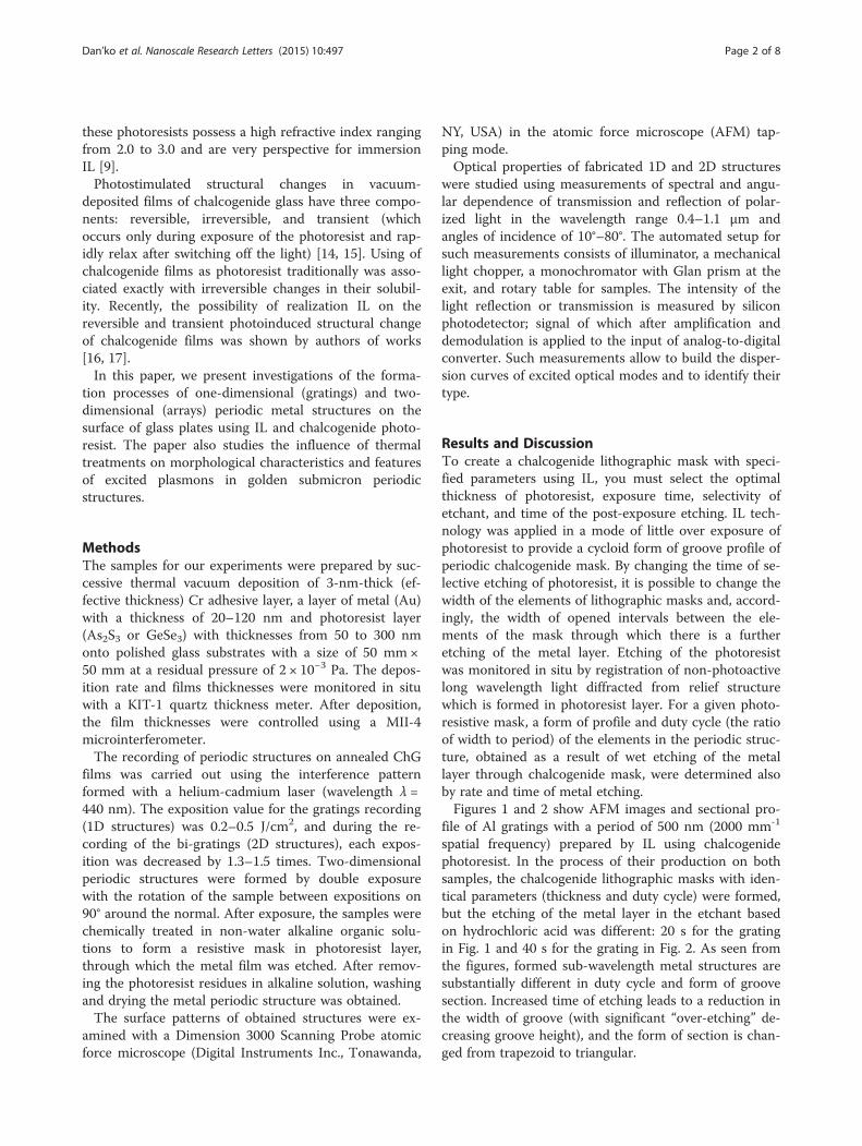
by IL using chalcogenide photoresist. It was found thatthe optimum temperature for our samples with Authicknesses from 30 to 60 nm is 400 °C—at lower tem-peratures insufficient effect of annealing, at 450 °C be-gins formation of agglomerates and disordering of thestructure.Figure 3 shows AFM image and cross-sectional profile
of the Au grating with period of 500 nm formed by ILon a glass substrate. Duty cycle of the structure is closeto 50 %, thickness of the gold is 35 nm, and the groovesectional form is trapezoid, even close to rectangular.This grating was annealed in vacuum at 400 °C for
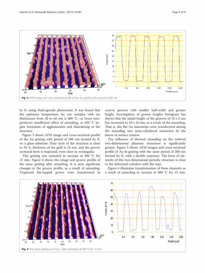
15 min. Figure 4 shows the image and groove profile ofthe same grating after annealing. It is seen significantchanges in the groove profile, as a result of annealing.Trapezoid flat-topped groves were transformed in
convex grooves with smaller half-width and greaterheight. Investigation of groove heights histogram hasshown that the initial height of the grooves of 35 ± 2 nmhas increased to 54 ± 10 nm, as a result of the annealing.That is, the flat Au nanostrips were transformed duringthe annealing into semi-cylindrical nanowires by theforces of surface tension.The influence of thermal annealing on the ordered
two-dimensional plasmon structures is significantlygreater. Figure 5 shows AFM images and cross-sectionalprofile of Au bi-grating with the same period of 500 nmformed by IL with a double exposure. The form of ele-ments of this two-dimensional periodic structure is closeto the deformed cylinders with flat tops.Figure 6 illustrates transformation of these elements as
a result of annealing in vacuum at 400 °C for 15 min.
Fig. 3 AFM image and cross-sectional profile of the Au grating with period of 500 nm
Fig. 4 The same grating as in Fig. 3 after annealing at 400 °C for 15 min
Dan’ko et al. Nanoscale Research Letters (2015) 10:497 Page 4 of 8

Cylindrical form of Au island was transformed intodome-shaped with a smaller half-width and much higheraltitude. The initial height of the elements of 34 ± 2 nmhas increased up to 64 ± 12 nm, as a result of annealing.This is significantly higher than for gratings, as in thiscase, «shrinkage» of Au island is two-dimensional, incontrast to the grating, where the process is one-dimensional.Modification of morphological characteristics of the
plasmon structures have displayed in their optical char-acteristics. The extinction of incident P-polarized light,αd = ln((1-R)/T) (where R—reflectance, T—transmit-tance) is shown in Figs. 7 and 8 for gratings from Figs. 3and 4 and two-dimensional structures from Figs. 5 and6, accordingly. Bands of high extinction are the result ofa resonant excitation of surface plasmon polaritons
(SPPs) and local plasmons (LP), mapping thereby thedispersion curves of the plasmon resonances.The spectral-angular position of the resonance peak of
the incident radiation conversion into surface plasmonpolariton waves is determined by equating the compo-nents of SPP wave vector and wave vector of the inci-dent radiation, which parallel to the interface betweenthe metal and non-metallic environment [19, 20]:
k sinθ þmG ¼ kPP; ð1Þ
where k = 2π/(λ/n)—wave vector of the incident radi-ation with a wavelength λ in a vacuum; θ—angle of inci-dence; m—an integer (m ≠ 0) and denotes the diffractionorder; G = 2π/a—reciprocal vector of grating with a
Fig. 5 AFM image and cross-sectional profile of laterally ordered Au two-dimensional structure with a period of 500 nm
Fig. 6 The same two-dimensional structure as in Fig. 5 after annealing at 400 °C for 15 min
Dan’ko et al. Nanoscale Research Letters (2015) 10:497 Page 5 of 8

period of a, ε = n2—permittivity and refractive index ofthe environment; and kPP—wave vector of SPP.To estimate approximately the magnitude of SPP wave
vector, the expression, obtained for a flat interface oftwo semi-infinite media [19], can be applied
kPP ¼ � 2π= λ=nð Þð Þ εMeε= εMe þ εð Þ½ �1=2; ð2Þ
where kPP has “+” sign at m > 0 and “−” at m < 0. Here,εMe = ε′Me + iε″Me = (n + ik)2—complex permittivity ofthe metal at the wavelength λ.
By using the expressions (1–2), the dispersion curvesfor SPPs, excited at interfaces metal/air or metal/sub-strate, were built in the coordinates “angle of excitation”versus “wavelength,” which is shown in Figs. 7 and 8.For calculations, the optical constants of gold from [21]were used, and the refractive index of the substrate wastaken equal to ns = 1.48. For a given gratings geometryand optical constants, it is possible excitation of modeswith m = +1 (1, 1s); m = +2 (2, 2s); m = −1 (1′, 1s′); m =−2 (2′, 2s′); at the interface air/gold (1, 1′, 2, 2′) andgold/substrate (1s, 1s′, 2s, 2s′).
a b
Fig. 7 P-polarized extinction as a function of wavelength and angle of incidence, of Au grating with period of 500 nm unannealed (a) andannealed at 400 °C for 15 min (b) overlapped with the dispersion curves calculated from Eqs. (1) and (2): the dispersion curves of the surfaceplasmon polaritons corresponding to the air-metal interface (1, 1′, 2′) and substrate-metal interface (1s, 1s′, 2s, 2s′) for m = +1 (1, 1s), m = +2 (2s),m = −1 (1′, 1s′) and m = −2 (2s′) diffraction orders. The color bar shows extinction with red representing high extinction
a b
Fig. 8 P-polarized extinction as a function of wavelength and angle of incidence, of Au two-dimensional structure with a period of 500 nmunannealed (a) and annealed at 400 °C for 15 min (b) overlapped with the dispersion curves calculated from Eqs. (1) and (2): the dispersion curvesof the surface plasmon polaritons corresponding to the air-metal interface (1, 1′, 2′) and substrate-metal interface (1s, 1s′, 2s, 2s′) for m = +1 (1, 1s),m = +2 (2s), m = −1 (1′, 1 s′) and m = −2 (2s′) diffraction orders. The color bar shows extinction with red representing high extinction
Dan’ko et al. Nanoscale Research Letters (2015) 10:497 Page 6 of 8

The peculiarity of LP excitation in a periodic array ofnanowires is a weak dependence of the LP resonancespectral position on the angle of incidence [22], which ismostly due to angular dependence of the width of nano-wires projection in the plane of light wave vector kx. Toestimate the upper high-frequency spectral position ofthe LP resonance, one can use the formula for thepolarization α of the spherical metal nanoparticle in di-electric environment [23]:
α ¼ εMe=ε−1ð Þ= εMe=εþ 2ð Þ; ð3Þ
which in the case of gold nanoparticle in a vacuumreaches a maximum in the vicinity of λ ~ 0.5 μm. Withincreasing the nanoparticle size (width of nanowires)and/or dielectric constant of the environment, the reson-ant wavelength can significantly increase [24] and reachthe infrared region of the spectrum; it also increases if inthe nearest vicinity other metal nanoparticles are loca-ted—due to the interaction between them.Excited SPP waves with m = −1 are most intense on
the unannealed samples of diffraction gratings (1′, 1s′Fig. 7a), because the edges of grating grooves (nano-wires) are closer to each other, than in annealed struc-tures, and SPP meets with less resistance when spreadalong the surface. Due to considerable contact area be-tween nanowires and substrate for the unannealed sam-ples, the mode, which excited on the gold-substrateinterface (1s′ on Fig. 7a), is intense. Excitation of LP ishardly noticeable on the background of intense SPPs.After annealing, due to «shrinkage» of Au nanowires
and islands in a more compact structure and, conse-quently, increase the distance between the edges ofnanowires or nanodots, the intensity of SPP decreases,especially decreases mode 1s′, while mode 1′ (excitedon the gold/air interface) remains moderately intense(Fig. 7b). Also, after annealing on the background of asignificant reduction of SPP intensity, the LP intensityincreases significantly, which is most clearly seen on theannealed 2D structure (Fig. 8b) in spectral region λ =0.6–0.8 μm.
ConclusionsIt is shown that IL technology using vacuumchalcogenide photoresist in combination with add-itional thermal treatment enabled the successful fabri-cation of uniform plasmonic structures with requiredcharacteristics (spatial frequency, depth of relief, aform of element profile) on a large area substrates(up to 25 cm2). The results of optical measurementconfirm the excitation of surface plasmon polaritonand local surface plasmon resonance in fabricatedsamples, spectral, and angular position of which coin-cides with the predictions of the theory and can be
adjusted over a wide range by selecting the geometricparameters of structures and technological modes oftheir manufacturing.
AbbreviationsAFM: atomic force microscope; ChG: chalcogenide glasses; IL: interferencelithography; LP: local plasmons; SPPs: surface plasmon polaritons.
Competing interestsThe authors declare that they have no competing interests.
Authors’ contributionsThe idea of the study was conceived by VD, II, and MD. The technologies ofinterference lithography and thermal treatment were developed andreleased by VM, PS, and ML. The AFM investigations were realized by PL andII, and SM proposed the first variant of the manuscript. All authors read andapproved the final version of the manuscript.
Received: 30 November 2015 Accepted: 14 December 2015
References1. Stewart ME, Anderton CR, Thompson LB, Maria J, Gray SK, Rogers JA, Nuzzo
RG (2008) Nanostructured plasmonic sensors. Chem Rev 108:494–5212. Jin ML, Pully V, Otto C, van den Berg A, Carlen ET (2010) High-density
periodic arrays of self-aligned subwavelength nanopyramids for surface-enhanced Raman spectroscopy. J Phys Chem C 114:21953–21959
3. Paivanranta B, Baroni P, Scharf T, Nakagawa W, Kuittinen M, Herzig HP(2008) Antireflective nanostructured microlenses. Microelectron Eng5:1089–1091
4. Cattoni A, Cambril E, Decanini D, Faini G, Haghiri-Gosnet AM (2010) Soft UV-NIL at 20 nm scale using flexible bi-layer stamp casted on HSQ mastermold. Microelectron Eng 87:1015–1018
5. Fu Y, Kok N, Bryan A, Zhou W (2004) Quasi-direct writing of diffractivestructures with a focused ion beam. Opt Express 12:1803
6. Zhang XY, Whitney AV, Zhao J, Hicks EM, Van Duyne RP (2006) Advances incontemporary nanosphere lithographic techniques. J Nanosci Nanotechnol6:1920–1934
7. Chuang SY, Chen HL, Kuo SS, Lai YH, Lee CC (2008) Using directnanoimprinting to study extraordinary transmission in textured metal films.Opt Express 16:2415
8. Brizuela F, Wang Y, Brewer CA et al (2009) Microscopy of extreme ultravioletlithography masks with 13.2 nm tabletop laser illumination. Opt Lett34:271–273
9. Dan’ko V, Indutnyi I, Min’ko V, Shepelyavyi P (2010) Interferencephotolithography with the use of resists on the basis of chalcogenideglassy semiconductors. Optoelectronics Instrum Data Process46:483–490
10. Vala M, Homola J (2014) Flexible method based on four-beam interferencelithography for fabrication of large areas of perfectly periodic plasmonicarrays. Opt Express 22:18778
11. Zankovych S, Hoffmann T, Seekamp J, Bruch JU, Sotomayor-Torres CM(2001) Nanoimprint lithography: challenges and prospects. Nanotechnology12:91–95
12. Indutnyi I, Min’ko V, Shepelyavyi P, Sopinskyy M, Tkach V, Dan’ko V (2011)Growth of the photonic nanostructures using interference lithography andoblique deposition in vacuum. Optoelectronika I Poluprovodnikova Tehnika(Ukraine) 46:47–54
13. Wong SH, Thiel M, Brodersen P, Fenske D, Ozin GA, Wegener M, vonFreymann G (2007) Highly selective wet etch for high-resolution three-dimensional nanostructures in arsenic sulfide all-inorganic photoresist.Chem Mater 19:4213–4221
14. Indutnyy I, Kostyshyn M, Kasjarum I, Min’ko V, Michailovska E, Romanenko P(1992) Photostimulated interactions in metal-semiconductor structures.Naukova Dumka, Kyiv, p 240
15. Kolobov AV, Tanaka K (1998) Nanoscale mechanism of photo-inducedmetastability and reversible photodarkening in chalcogenide vitreoussemiconductors. Phizika i Tehnika Poluprovodnikov (Russia) 32:899–904
16. Dan’ko V, Indutnyi I, Min’ko V, Shepeliavyi P, Berezn’ova O, Lytvyn O (2012)Photoinduced etching of thin films of chalcogenide glassy semiconductors.Semiconductors 46:504–508
Dan’ko et al. Nanoscale Research Letters (2015) 10:497 Page 7 of 8

17. Dan’ko V, Indutnyi I, Min’ko V, Shepeliavyi P, Lykanyuk M, Litvin O (2012)Interference photolithography using photoetching effect in chalcogenidefilms. J Non-Oxide Glasses 3:13–18
18. Yukhymchuk VO, Kostyukevych SA, Dzhagan VM, Milekhin AG, Rodyakina EE,Yanchuk IB, Shepeliavy PY, Valakh MY, Kostyukevych KV, Lysiuk VO,Tverdokhlib IV (2012) SERS of Rhodamine 6G on substrates with laterallyordered and random gold nanoislands. Semicond Phys Quantum ElectronOptoelectron 15:232–238
19. Dmitruk NL, Litovchenko VG, Strygewskyy VL (1989) Surface polaritons insemiconductors and dielectrics. Naukova Dumka, Kyiv, p 375
20. Surface polaritons. Electromagnetic waves on the surfaces and interfacesUnder. Agranovich VM, Mills DL (ed). Nauka, Moscow; 1985. p 525
21. Johnson PB, Christy RW (1972) Optical constants of the noble metals. PhysRev B 6:4370–4379
22. Sosnova MV, Dmitruk NL, Korovin AV, Mamykin SV (2010) Local plasmonexcitations in one-dimensional array of metal nanowires for sensorapplications. Appl Phys B Lasers Opt Springer 99:493–497
23. Bohren CF, Huffman DR (1998) Absorption and scattering of light by smallparticles. Wiley Interscience, New York, p 544
24. Dmitruk NL, Malinich SZ (2014) Surface plasmon resonances and theirmanifestation in the optical properties of nanostructures of noble metals.Ukr J Phys Rev 9:3–37
Submit your manuscript to a journal and benefi t from:
7 Convenient online submission
7 Rigorous peer review
7 Immediate publication on acceptance
7 Open access: articles freely available online
7 High visibility within the fi eld
7 Retaining the copyright to your article
Submit your next manuscript at 7 springeropen.com
Dan’ko et al. Nanoscale Research Letters (2015) 10:497 Page 8 of 8