Embed Size (px)
Citation preview
© 2009 Microchip Technology Inc. Preliminary DS39933C
PIC18F87J90 FamilyData Sheet
64/80-Pin, High-PerformanceMicrocontrollers with LCD Driver
and nanoWatt Technology
DS39933C-page ii Preliminary © 2009 Microchip Technology Inc.
Information contained in this publication regarding deviceapplications and the like is provided only for your convenienceand may be superseded by updates. It is your responsibility toensure that your application meets with your specifications.MICROCHIP MAKES NO REPRESENTATIONS ORWARRANTIES OF ANY KIND WHETHER EXPRESS ORIMPLIED, WRITTEN OR ORAL, STATUTORY OROTHERWISE, RELATED TO THE INFORMATION,INCLUDING BUT NOT LIMITED TO ITS CONDITION,QUALITY, PERFORMANCE, MERCHANTABILITY ORFITNESS FOR PURPOSE. Microchip disclaims all liabilityarising from this information and its use. Use of Microchipdevices in life support and/or safety applications is entirely atthe buyer’s risk, and the buyer agrees to defend, indemnify andhold harmless Microchip from any and all damages, claims,suits, or expenses resulting from such use. No licenses areconveyed, implicitly or otherwise, under any Microchipintellectual property rights.
Trademarks
The Microchip name and logo, the Microchip logo, Accuron, dsPIC, KEELOQ, KEELOQ logo, MPLAB, PIC, PICmicro, PICSTART, rfPIC, SmartShunt and UNI/O are registered trademarks of Microchip Technology Incorporated in the U.S.A. and other countries.
FilterLab, Linear Active Thermistor, MXDEV, MXLAB, SEEVAL, SmartSensor and The Embedded Control Solutions Company are registered trademarks of Microchip Technology Incorporated in the U.S.A.
Analog-for-the-Digital Age, Application Maestro, CodeGuard, dsPICDEM, dsPICDEM.net, dsPICworks, dsSPEAK, ECAN, ECONOMONITOR, FanSense, In-Circuit Serial Programming, ICSP, ICEPIC, Mindi, MiWi, MPASM, MPLAB Certified logo, MPLIB, MPLINK, mTouch, PICkit, PICDEM, PICDEM.net, PICtail, PIC32 logo, PowerCal, PowerInfo, PowerMate, PowerTool, REAL ICE, rfLAB, Select Mode, Total Endurance, WiperLock and ZENA are trademarks of Microchip Technology Incorporated in the U.S.A. and other countries.
SQTP is a service mark of Microchip Technology Incorporated in the U.S.A.
All other trademarks mentioned herein are property of their respective companies.
© 2009, Microchip Technology Incorporated, Printed in the U.S.A., All Rights Reserved.
Printed on recycled paper.
Note the following details of the code protection feature on Microchip devices:• Microchip products meet the specification contained in their particular Microchip Data Sheet.
• Microchip believes that its family of products is one of the most secure families of its kind on the market today, when used in the intended manner and under normal conditions.
• There are dishonest and possibly illegal methods used to breach the code protection feature. All of these methods, to our knowledge, require using the Microchip products in a manner outside the operating specifications contained in Microchip’s Data Sheets. Most likely, the person doing so is engaged in theft of intellectual property.
• Microchip is willing to work with the customer who is concerned about the integrity of their code.
• Neither Microchip nor any other semiconductor manufacturer can guarantee the security of their code. Code protection does not mean that we are guaranteeing the product as “unbreakable.”
Code protection is constantly evolving. We at Microchip are committed to continuously improving the code protection features of ourproducts. Attempts to break Microchip’s code protection feature may be a violation of the Digital Millennium Copyright Act. If such actsallow unauthorized access to your software or other copyrighted work, you may have a right to sue for relief under that Act.
Microchip received ISO/TS-16949:2002 certification for its worldwide headquarters, design and wafer fabrication facilities in Chandler and Tempe, Arizona; Gresham, Oregon and design centers in California and India. The Company’s quality system processes and procedures are for its PIC® MCUs and dsPIC® DSCs, KEELOQ® code hopping devices, Serial EEPROMs, microperipherals, nonvolatile memory and analog products. In addition, Microchip’s quality system for the design and manufacture of development systems is ISO 9001:2000 certified.
© 2009 Microchip Technology Inc. Preliminary DS39933C-page 1
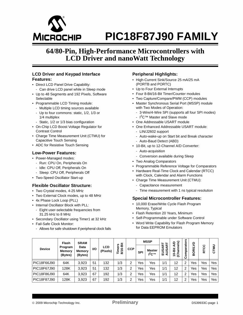
PIC18F87J90 FAMILY
LCD Driver and Keypad Interface Features:• Direct LCD Panel Drive Capability:
- Can drive LCD panel while in Sleep mode• Up to 48 Segments and 192 Pixels, Software
Selectable• Programmable LCD Timing module:
- Multiple LCD timing sources available- Up to four commons: static, 1/2, 1/3 or
1/4 multiplex- Static, 1/2 or 1/3 bias configuration
• On-Chip LCD Boost Voltage Regulator for Contrast Control
• Charge Time Measurement Unit (CTMU) for Capacitive Touch Sensing
• ADC for Resistive Touch Sensing
Low-Power Features:• Power-Managed modes:
- Run: CPU On, Peripherals On- Idle: CPU Off, Peripherals On- Sleep: CPU Off, Peripherals Off
• Two-Speed Oscillator Start-up
Flexible Oscillator Structure:• Two Crystal modes, 4-25 MHz• Two External Clock modes, up to 48 MHz• 4x Phase Lock Loop (PLL)• Internal Oscillator Block with PLL:
- Eight user-selectable frequencies from 31.25 kHz to 8 MHz
• Secondary Oscillator using Timer1 at 32 kHz• Fail-Safe Clock Monitor:
- Allows for safe shutdown if peripheral clock fails
Peripheral Highlights:• High-Current Sink/Source 25 mA/25 mA
(PORTB and PORTC)• Up to Four External Interrupts• Four 8-Bit/16-Bit Timer/Counter modules• Two Capture/Compare/PWM (CCP) modules• Master Synchronous Serial Port (MSSP) module
with Two Modes of Operation:- 3-Wire/4-Wire SPI (supports all four SPI modes)- I2C™ Master and Slave mode
• One Addressable USART module• One Enhanced Addressable USART module:
- LIN/J2602 support- Auto-wake-up on Start bit and Break character- Auto-Baud Detect (ABD)
• 10-Bit, up to 12-Channel A/D Converter: - Auto-acquisition- Conversion available during Sleep
• Two Analog Comparators• Programmable Reference Voltage for Comparators• Hardware Real-Time Clock and Calendar (RTCC)
with Clock, Calendar and Alarm Functions• Charge Time Measurement Unit (CTMU):
- Capacitance measurement- Time measurement with 1 ns typical resolution
Special Microcontroller Features:• 10,000 Erase/Write Cycle Flash Program
Memory, Typical• Flash Retention 20 Years, Minimum• Self-Programmable under Software Control• Word Write Capability for Flash Program Memory
for Data EEPROM Emulators
Device
FlashProgram Memory(Bytes)
SRAMData
Memory(Bytes)
I/O LCD(Pixels) Ti
mer
s 8
/16-
Bit
CCP
MSSP
EUSA
RT
AU
SAR
T
10-B
it A
/D(C
hann
els)
Com
para
tors
BO
R/L
VD
RTC
C
CTM
U
SPI MasterI2C™
PIC18F66J90 64K 3,923 51 132 1/3 2 Yes Yes 1/1 12 2 Yes Yes YesPIC18F67J90 128K 3,923 51 132 1/3 2 Yes Yes 1/1 12 2 Yes Yes YesPIC18F86J90 64K 3,923 67 192 1/3 2 Yes Yes 1/1 12 2 Yes Yes YesPIC18F87J90 128K 3,923 67 192 1/3 2 Yes Yes 1/1 12 2 Yes Yes Yes
64/80-Pin, High-Performance Microcontrollers withLCD Driver and nanoWatt Technology

PIC18F87J90 FAMILY
DS39933C-page 2 Preliminary © 2009 Microchip Technology Inc.
Special Microcontroller Features(Continued):• Priority Levels for Interrupts• 8 x 8 Single-Cycle Hardware Multiplier• Extended Watchdog Timer (WDT):
- Programmable period from 4 ms to 131s
• In-Circuit Serial Programming™ (ICSP™) via Two Pins
• In-Circuit Debug via Two Pins• Operating Voltage Range: 2.0V to 3.6V• 5.5V Tolerant Input (digital pins only)• Selectable Open-Drain Configuration for Serial
Communication and CCP Pins for Driving Outputs up to 5V
• On-Chip 2.5V Regulator
© 2009 Microchip Technology Inc. Preliminary DS39933C-page 3
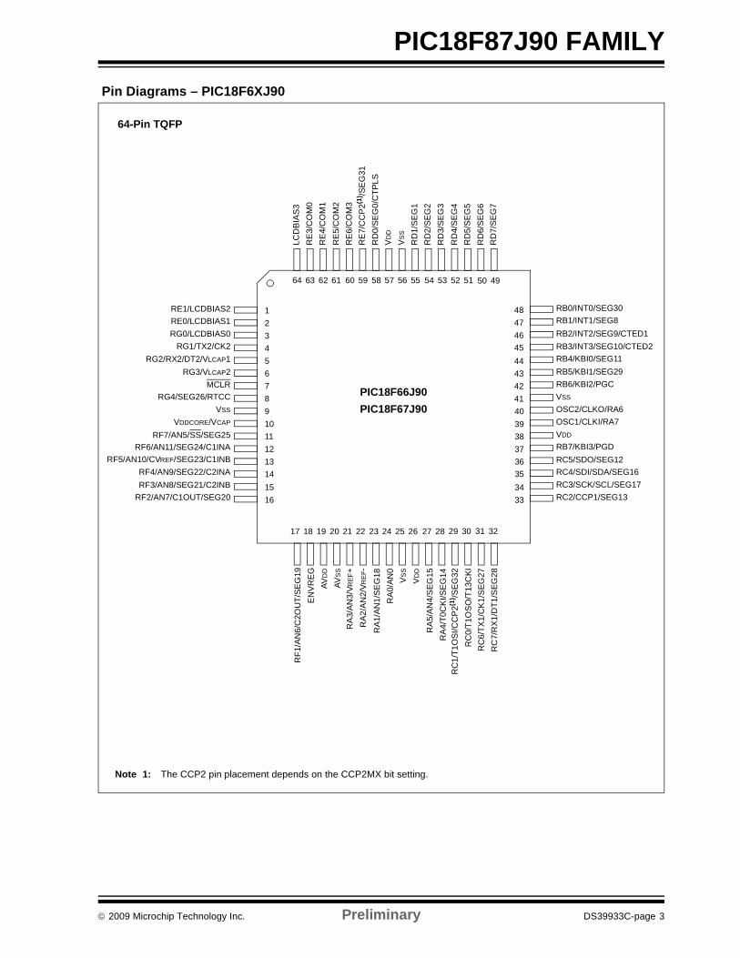
PIC18F87J90 FAMILY Pin Diagrams – PIC18F6XJ90
64-Pin TQFP
50 49
LCD
BIA
S3
RE
3/C
OM
0R
E4/
CO
M1
RE
5/C
OM
2R
E6/
CO
M3
RE
7/C
CP
2(1) /S
EG
31R
D0/
SE
G0/
CTP
LSV
DD
VS
S
RD
1/S
EG
1R
D2/
SE
G2
RD
3/S
EG
3R
D4/
SE
G4
RD
5/S
EG
5R
D6/
SE
G6
RD
7/S
EG
7
RE1/LCDBIAS2RE0/LCDBIAS1RG0/LCDBIAS0
RG1/TX2/CK2RG2/RX2/DT2/VLCAP1
RG3/VLCAP2MCLR
RG4/SEG26/RTCCVSS
VDDCORE/VCAP
RF7/AN5/SS/SEG25RF6/AN11/SEG24/C1INA
RF5/AN10/CVREF/SEG23/C1INBRF4/AN9/SEG22/C2INARF3/AN8/SEG21/C2INB
RF2/AN7/C1OUT/SEG20
RB0/INT0/SEG30RB1/INT1/SEG8RB2/INT2/SEG9/CTED1RB3/INT3/SEG10/CTED2RB4/KBI0/SEG11RB5/KBI1/SEG29RB6/KBI2/PGCVSS
OSC2/CLKO/RA6OSC1/CLKI/RA7VDD
RB7/KBI3/PGD
RC4/SDI/SDA/SEG16RC3/SCK/SCL/SEG17RC2/CCP1/SEG13
EN
VR
EG
RF1
/AN
6/C
2OU
T/SE
G19
AVD
D
AVS
S
RA
3/A
N3/
VRE
F+R
A2/
AN
2/V R
EF-
RA
1/AN
1/S
EG
18R
A0/
AN0
VS
S
VD
D
RA
4/T0
CK
I/SE
G14
RA
5/A
N4/
SEG
15
RC
1/T1
OS
I/CC
P2(1
) /SEG
32R
C0/
T1O
SO
/T13
CKI
RC
7/R
X1/
DT1
/SEG
28R
C6/
TX1/
CK
1/S
EG27
RC5/SDO/SEG12
54 53 52 5158 57 56 5560 5964 63 62 61
Note 1: The CCP2 pin placement depends on the CCP2MX bit setting.
PIC18F66J90PIC18F67J90
12345678910111213141516
17 18 19 20 21 22 23 24 25 26 3127 28 29 30 32
383736353433
4039
4847464544434241
PIC18F87J90 FAMILY
DS39933C-page 4 Preliminary © 2009 Microchip Technology Inc.
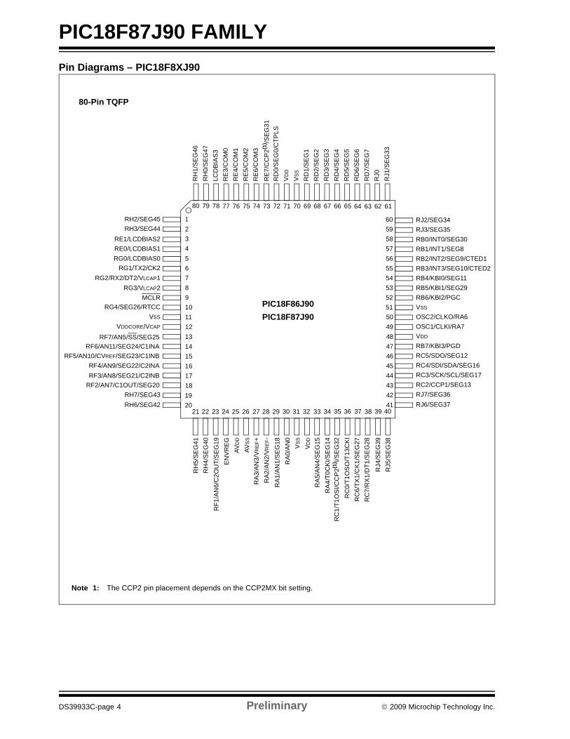
Pin Diagrams – PIC18F8XJ90
80-Pin TQFP
345678910111213141516
4847464544434241
4039
64 63 62 61
21 22 23 24 25 26 27 28 29 30 31 32
LCD
BIA
S3
RE
3/C
OM
0R
E4/
CO
M1
RE
5/C
OM
2R
E6/
CO
M3
RE
7/C
CP
2(1) /S
EG31
RD
0/S
EG
0/C
TPLS
VD
D
VS
S
RD
1/S
EG
1R
D2/
SE
G2
RD
3/S
EG
3R
D4/
SE
G4
RD
5/S
EG
5R
D6/
SE
G6
RD
7/S
EG
7
RE1/LCDBIAS2RE0/LCDBIAS1RG0/LCDBIAS0
RG1/TX2/CK2RG2/RX2/DT2/VLCAP1
RG3/VLCAP2MCLR
RG4/SEG26/RTCCVSS
VDDCORE/VCAP
VSS
OSC2/CLKO/RA6OSC1/CLKI/RA7VDD
EN
VR
EGR
F1/A
N6/
C2O
UT/
SE
G19
AVD
D
AVS
S
RA
3/A
N3/
VRE
F+R
A2/A
N2/
VRE
F-R
A1/
AN
1/S
EG
18R
A0/
AN
0V
SS
VDD
RJ0
RJ1
/SE
G33
RH
1/S
EG
46R
H0/
SE
G47
12
RH2/SEG45RH3/SEG44
1718
RH7/SEG43RH6/SEG42
RH
5/S
EG
41R
H4/
SE
G40
RJ5
/SE
G38
RJ4
/SE
G39
37
RJ7/SEG36RJ6/SEG37
5049
RJ2/SEG34RJ3/SEG35
1920
33 34 35 36 38
5857565554535251
6059
68 67 66 6572 71 70 6974 7378 77 76 757980
RB0/INT0/SEG30RB1/INT1/SEG8RB2/INT2/SEG9/CTED1RB3/INT3/SEG10/CTED2RB4/KBI0/SEG11RB5/KBI1/SEG29RB6/KBI2/PGC
RB7/KBI3/PGD
RC2/CCP1/SEG13
RC5/SDO/SEG12
RA
4/T0
CK
I/SE
G14
RA
5/A
N4/
SE
G15
RC
1/T1
OS
I/CC
P2(1
) I/S
EG
32R
C0/
T1O
SO
/T13
CK
I
RC
7/R
X1/
DT1
/SE
G28
RC
6/TX
1/C
K1/S
EG
27
RF7/AN5/SS/SEG25RF6/AN11/SEG24/C1INA
RF5/AN10/CVREF/SEG23/C1INBRF4/AN9/SEG22/C2INARF3/AN8/SEG21/C2INB
RF2/AN7/C1OUT/SEG20
RC4/SDI/SDA/SEG16RC3/SCK/SCL/SEG17
Note 1: The CCP2 pin placement depends on the CCP2MX bit setting.
PIC18F86J90PIC18F87J90
© 2009 Microchip Technology Inc. Preliminary DS39933C-page 5
PIC18F87J90 FAMILYTable of Contents1.0 Device Overview .......................................................................................................................................................................... 72.0 Oscillator Configurations ............................................................................................................................................................ 293.0 Power-Managed Modes ............................................................................................................................................................. 394.0 Reset .......................................................................................................................................................................................... 475.0 Memory Organization ................................................................................................................................................................. 596.0 Flash Program Memory.............................................................................................................................................................. 837.0 8 x 8 Hardware Multiplier............................................................................................................................................................ 938.0 Interrupts .................................................................................................................................................................................... 959.0 I/O Ports ................................................................................................................................................................................... 11110.0 Timer0 Module ......................................................................................................................................................................... 13311.0 Timer1 Module ......................................................................................................................................................................... 13712.0 Timer2 Module ......................................................................................................................................................................... 14313.0 Timer3 Module ......................................................................................................................................................................... 14514.0 Real-Time Clock and Calendar (RTCC)................................................................................................................................... 14915.0 Capture/Compare/PWM (CCP) Modules ................................................................................................................................. 16716.0 Liquid Crystal Display (LCD) Driver Module............................................................................................................................. 17717.0 Master Synchronous Serial Port (MSSP) Module .................................................................................................................... 20518.0 Enhanced Universal Synchronous Asynchronous Receiver Transmitter (EUSART) ............................................................... 24919.0 Addressable Universal Synchronous Asynchronous Receiver Transmitter (AUSART) ........................................................... 26920.0 10-bit Analog-to-Digital Converter (A/D) Module...................................................................................................................... 28321.0 Comparator Module.................................................................................................................................................................. 29322.0 Comparator Voltage Reference Module................................................................................................................................... 29923.0 Charge Time Measurement Unit (CTMU) ................................................................................................................................ 30324.0 Special Features of the CPU.................................................................................................................................................... 31925.0 Instruction Set Summary .......................................................................................................................................................... 33326.0 Development Support............................................................................................................................................................... 38327.0 Electrical Characteristics .......................................................................................................................................................... 38728.0 Packaging Information.............................................................................................................................................................. 421Appendix A: Revision History............................................................................................................................................................. 427Appendix B: Migration From PIC18F85J90 to PIC18F87J90 ............................................................................................................ 427The Microchip Web Site ..................................................................................................................................................................... 439Customer Change Notification Service .............................................................................................................................................. 439Customer Support .............................................................................................................................................................................. 439Reader Response .............................................................................................................................................................................. 440Product Identification System ............................................................................................................................................................ 441

PIC18F87J90 FAMILY
DS39933C-page 6 Preliminary © 2009 Microchip Technology Inc.
TO OUR VALUED CUSTOMERSIt is our intention to provide our valued customers with the best documentation possible to ensure successful use of your Microchipproducts. To this end, we will continue to improve our publications to better suit your needs. Our publications will be refined andenhanced as new volumes and updates are introduced. If you have any questions or comments regarding this publication, please contact the Marketing Communications Department viaE-mail at [email protected] or fax the Reader Response Form in the back of this data sheet to (480) 792-4150. Wewelcome your feedback.
Most Current Data SheetTo obtain the most up-to-date version of this data sheet, please register at our Worldwide Web site at:
http://www.microchip.comYou can determine the version of a data sheet by examining its literature number found on the bottom outside corner of any page.The last character of the literature number is the version number, (e.g., DS30000A is version A of document DS30000).
ErrataAn errata sheet, describing minor operational differences from the data sheet and recommended workarounds, may exist for currentdevices. As device/documentation issues become known to us, we will publish an errata sheet. The errata will specify the revisionof silicon and revision of document to which it applies.To determine if an errata sheet exists for a particular device, please check with one of the following:• Microchip’s Worldwide Web site; http://www.microchip.com• Your local Microchip sales office (see last page)When contacting a sales office, please specify which device, revision of silicon and data sheet (include literature number) you areusing.
Customer Notification SystemRegister on our web site at www.microchip.com to receive the most current information on all of our products.
© 2009 Microchip Technology Inc. Preliminary DS39933C-page 7
PIC18F87J90 FAMILY
1.0 DEVICE OVERVIEWThis document contains device-specific information forthe following devices:
This family combines the traditional advantages of allPIC18 microcontrollers – namely, high computationalperformance and a rich feature set – with a versatileon-chip LCD driver, while maintaining an extremelycompetitive price point. These features make thePIC18F87J90 family a logical choice for manyhigh-performance applications where price is a primaryconsideration.
1.1 Core Features
1.1.1 nanoWatt TECHNOLOGYAll of the devices in the PIC18F87J90 family incorporatea range of features that can significantly reduce powerconsumption during operation. Key items include:• Alternate Run Modes: By clocking the controller
from the Timer1 source or the internal RC oscillator, power consumption during code execution can be reduced by as much as 90%.
• Multiple Idle Modes: The controller can also run with its CPU core disabled but the peripherals still active. In these states, power consumption can be reduced even further, to as little as 4% of normal operation requirements.
• On-the-Fly Mode Switching: The power-managed modes are invoked by user code during operation, allowing the user to incorporate power-saving ideas into their application’s software design.
1.1.2 OSCILLATOR OPTIONS AND FEATURES
All of the devices in the PIC18F87J90 family offer sixdifferent oscillator options, allowing users a range ofchoices in developing application hardware. Theseinclude:• Two Crystal modes, using crystals or ceramic
resonators.• Two External Clock modes, offering the option of
a divide-by-4 clock output.• A Phase Lock Loop (PLL) frequency multiplier,
available to the External Oscillator modes which allows clock speeds of up to 40 MHz. PLL can also be used with the internal oscillator.
• An internal oscillator block which provides an 8 MHz clock (±2% accuracy) and an INTRC source (approximately 31 kHz, stable over temperature and VDD), as well as a range of six user-selectable clock frequencies, between 125 kHz to 4 MHz, for a total of eight clock frequencies. This option frees the two oscillator pins for use as additional general purpose I/O.
The internal oscillator block provides a stable referencesource that gives the family additional features forrobust operation:• Fail-Safe Clock Monitor: This option constantly
monitors the main clock source against a reference signal provided by the internal oscillator. If a clock failure occurs, the controller is switched to the internal oscillator, allowing for continued low-speed operation or a safe application shutdown.
• Two-Speed Start-up: This option allows the internal oscillator to serve as the clock source from Power-on Reset, or wake-up from Sleep mode, until the primary clock source is available.
1.1.3 MEMORY OPTIONSThe PIC18F87J90 family provides ample room forapplication code, from 64 Kbytes to 128 Kbytes of codespace. The Flash cells for program memory are ratedto last up to 10,000 erase/write cycles. Data retentionwithout refresh is conservatively estimated to begreater than 20 years.The Flash program memory is readable and writable.During normal operation, the PIC18F87J90 family alsoprovides plenty of room for dynamic application datawith up to 3,923 bytes of data RAM.
1.1.4 EXTENDED INSTRUCTION SETThe PIC18F87J90 family implements the optionalextension to the PIC18 instruction set, adding 8 newinstructions and an Indexed Addressing mode.Enabled as a device configuration option, the extensionhas been specifically designed to optimize re-entrantapplication code originally developed in high-levellanguages, such as ‘C’.
1.1.5 EASY MIGRATIONRegardless of the memory size, all devices share thesame rich set of peripherals, allowing for a smoothmigration path as applications grow and evolve.
The consistent pinout scheme used throughout theentire family also aids in migrating to the next largerdevice. This is true when moving between the 64-pinmembers, between the 80-pin members, or evenjumping from 64-pin to 80-pin devices.
The PIC18F87J90 family is also largely pin compatiblewith other PIC18 families, such as the PIC18F8720 andPIC18F8722, the PIC18F85J11, and the PIC18F8490and PIC18F85J90 families of microcontrollers withLCD drivers. This allows a new dimension to theevolution of applications, allowing developers to selectdifferent price points within Microchip’s PIC18 portfolio,while maintaining a similar feature set.
• PIC18F66J90 • PIC18F86J90• PIC18F67J90 • PIC18F87J90
PIC18F87J90 FAMILY
DS39933C-page 8 Preliminary © 2009 Microchip Technology Inc.
1.2 LCD DriverThe on-chip LCD driver includes many features thatmake the integration of displays in low-powerapplications easier. These include an integrated volt-age regulator with charge pump that allows contrastcontrol in software and display operation above deviceVDD.
1.3 Other Special Features• Communications: The PIC18F87J90 family
incorporates a range of serial communication peripherals, including an Addressable USART, a separate Enhanced USART that supports LIN specification 1.2, and one Master SSP module capable of both SPI and I2C™ (Master and Slave) modes of operation.
• CCP Modules: All devices in the family incorporate two Capture/Compare/PWM (CCP) modules. Up to four different time bases may be used to perform several different operations at once.
• 10-Bit A/D Converter: This module incorporates programmable acquisition time, allowing for a channel to be selected and a conversion to be initiated without waiting for a sampling period and thus, reducing code overhead.
• Charge Time Measurement Unit (CTMU): The CTMU is a flexible analog module that provides accurate differential time measurement between pulse sources, as well as asynchronous pulse generation.
Together with other on-chip analog modules, theCTMU can precisely measure time, measurecapacitance or relative changes in capacitance, orgenerate output pulses that are independent of thesystem clock.
• Extended Watchdog Timer (WDT): This enhanced version incorporates a 16-bit prescaler, allowing an extended time-out range that is stable across operating voltage and temperature. See Section 27.0 “Electrical Characteristics” for time-out periods.
• Real Time Clock and Calendar Module (RTCC): The RTCC module is intended for applications requiring that accurate time be maintained for extended periods of time with minimum to no intervention from the CPU.
The module is a 100-year clock and calendar withautomatic leap-year detection. The range of theclock is from 00:00:00 (midnight) on January 1,2000 to 23:59:59 on December 31, 2099.
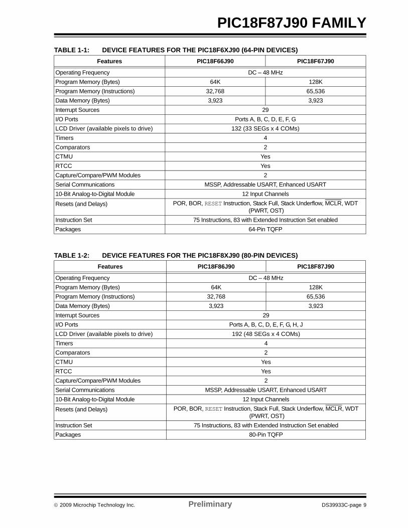
1.4 Details on Individual Family Members
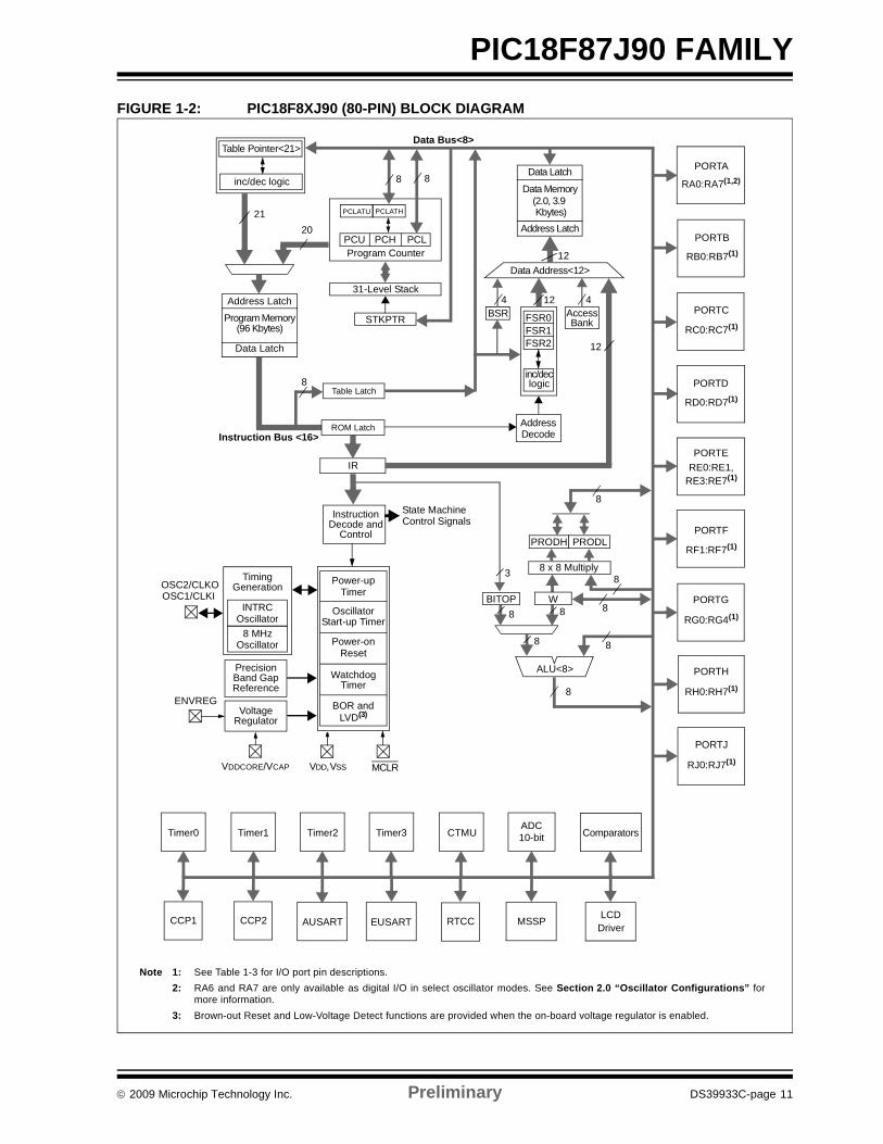
Devices in the PIC18F87J90 family are available in64-pin and 80-pin packages. Block diagrams for thetwo groups are shown in Figure 1-1 and Figure 1-2.
The devices are differentiated from each other in fourways:
1. Flash program memory (two sizes, 64 Kbytesfor PIC18FX6J90 devices and 128 Kbytes forPIC18FX7J90 devices).
2. Data RAM (3,923 bytes RAM for bothPIC18FX6J90 and PIC18FX7J90 devices).
3. I/O ports (7 bidirectional ports on PIC18F6XJ90devices, 9 bidirectional ports on PIC18F8XJ90devices).
4. LCD Pixels: 132 pixels (33 SEGs x 4 COMs) canbe driven by 64-pin devices; 192 pixels(48 SEGs x 4 COMs) can be driven by 80-pindevices.
All other features for devices in this family are identical.These are summarized in Table 1-1 and Table 1-2.
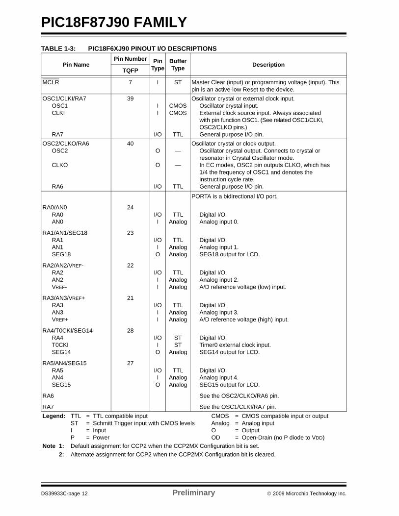
The pinouts for all devices are listed in Table 1-3 andTable 1-4.
© 2009 Microchip Technology Inc. Preliminary DS39933C-page 9
PIC18F87J90 FAMILYTABLE 1-1: DEVICE FEATURES FOR THE PIC18F6XJ90 (64-PIN DEVICES)
TABLE 1-2: DEVICE FEATURES FOR THE PIC18F8XJ90 (80-PIN DEVICES)
Features PIC18F66J90 PIC18F67J90
Operating Frequency DC – 48 MHzProgram Memory (Bytes) 64K 128KProgram Memory (Instructions) 32,768 65,536Data Memory (Bytes) 3,923 3,923Interrupt Sources 29I/O Ports Ports A, B, C, D, E, F, GLCD Driver (available pixels to drive) 132 (33 SEGs x 4 COMs)Timers 4Comparators 2CTMU YesRTCC YesCapture/Compare/PWM Modules 2Serial Communications MSSP, Addressable USART, Enhanced USART10-Bit Analog-to-Digital Module 12 Input Channels
Resets (and Delays) POR, BOR, RESET Instruction, Stack Full, Stack Underflow, MCLR, WDT (PWRT, OST)
Instruction Set 75 Instructions, 83 with Extended Instruction Set enabledPackages 64-Pin TQFP
Features PIC18F86J90 PIC18F87J90
Operating Frequency DC – 48 MHzProgram Memory (Bytes) 64K 128KProgram Memory (Instructions) 32,768 65,536Data Memory (Bytes) 3,923 3,923Interrupt Sources 29I/O Ports Ports A, B, C, D, E, F, G, H, JLCD Driver (available pixels to drive) 192 (48 SEGs x 4 COMs)Timers 4Comparators 2CTMU YesRTCC YesCapture/Compare/PWM Modules 2Serial Communications MSSP, Addressable USART, Enhanced USART10-Bit Analog-to-Digital Module 12 Input Channels
Resets (and Delays) POR, BOR, RESET Instruction, Stack Full, Stack Underflow, MCLR, WDT (PWRT, OST)
Instruction Set 75 Instructions, 83 with Extended Instruction Set enabledPackages 80-Pin TQFP
PIC18F87J90 FAMILY
DS39933C-page 10 Preliminary © 2009 Microchip Technology Inc.
FIGURE 1-1: PIC18F6XJ90 (64-PIN) BLOCK DIAGRAM
InstructionDecode and
Control
PORTAData Latch
Data Memory(2.0, 3.9
Address Latch
Data Address<12>12
AccessBSR FSR0FSR1FSR2
inc/declogic
Address
4 12 4
PCH PCL
PCLATH
8
31-Level Stack
Program Counter
PRODLPRODH
8 x 8 Multiply
8
BITOP88
ALU<8>
Address Latch
Program Memory(96 Kbytes)
Data Latch
20
8
8
Table Pointer<21>
inc/dec logic
21
8
Data Bus<8>
Table Latch8
IR
12
3
PCLATU
PCU
Note 1: See Table 1-3 for I/O port pin descriptions.2: RA6 and RA7 are only available as digital I/O in select oscillator modes. See Section 2.0 “Oscillator Configurations” for more
information3: Brown-out Reset and Low-Voltage Detect functions are provided when the on-board voltage regulator is enabled.
AUSART
Comparators
MSSP
Timer3Timer2 CTMUTimer1
CCP2
ADC10-bit
W
Instruction Bus <16>
STKPTR Bank
8
State MachineControl Signals
Decode
8
8
EUSART
ROM Latch
LCD
PORTC
PORTD
PORTE
PORTF
PORTG
RA0:RA7(1,2)
RC0:RC7(1)
RD0:RD7(1)
RE0:RE1,
RF1:RF7(1)
RG0:RG4(1)
PORTB
RB0:RB7(1)
OSC1/CLKIOSC2/CLKO
VDD,
TimingGeneration
VSS MCLR
Power-upTimer
OscillatorStart-up Timer
Power-onReset
WatchdogTimer
BOR andLVD(3)
Precision
ReferenceBand Gap
INTRCOscillator
RegulatorVoltage
VDDCORE/VCAP
ENVREG
Kbytes)
Driver
8 MHzOscillator
RE3:RE7(1)
Timer0
CCP1 RTCC
© 2009 Microchip Technology Inc. Preliminary DS39933C-page 11
PIC18F87J90 FAMILYFIGURE 1-2: PIC18F8XJ90 (80-PIN) BLOCK DIAGRAM
InstructionDecode and
Control
Data Latch
Data Memory(2.0, 3.9
Address Latch
Data Address<12>12
AccessBSR FSR0FSR1FSR2
inc/declogic
Address
4 12 4
PCH PCL
PCLATH
8
31-Level Stack
Program Counter
PRODLPRODH
8 x 8 Multiply
8
BITOP88
ALU<8>
Address Latch
Program Memory(96 Kbytes)
Data Latch
20
8
8
Table Pointer<21>
inc/dec logic
21
8
Data Bus<8>
Table Latch8
IR
12
3
PCLATU
PCU
W
Instruction Bus <16>
STKPTR Bank
8
State MachineControl Signals
Decode
8
8
ROM Latch
OSC1/CLKIOSC2/CLKO
VDD,VSS MCLR
Power-upTimer
OscillatorStart-up Timer
Power-onReset
WatchdogTimer
Precision
ReferenceBand Gap
RegulatorVoltage
VDDCORE/VCAP
ENVREG
Kbytes)
PORTA
PORTC
PORTD
PORTE
PORTF
PORTG
RA0:RA7(1,2)
RC0:RC7(1)
RD0:RD7(1)
RF1:RF7(1)
RG0:RG4(1)
PORTB
RB0:RB7(1)
PORTH
RH0:RH7(1)
PORTJ
RJ0:RJ7(1)
Note 1: See Table 1-3 for I/O port pin descriptions.2: RA6 and RA7 are only available as digital I/O in select oscillator modes. See Section 2.0 “Oscillator Configurations” for
more information.3: Brown-out Reset and Low-Voltage Detect functions are provided when the on-board voltage regulator is enabled.
TimingGeneration
INTRCOscillator
8 MHzOscillator
RE0:RE1,RE3:RE7(1)
BOR andLVD(3)
AUSART
Comparators
MSSP
Timer3Timer2 CTMUTimer1
CCP2
ADC10-bit
EUSARTLCD
Driver
Timer0
CCP1 RTCC
PIC18F87J90 FAMILY
DS39933C-page 12 Preliminary © 2009 Microchip Technology Inc.
TABLE 1-3: PIC18F6XJ90 PINOUT I/O DESCRIPTIONS
Pin NamePin Number Pin
TypeBufferType Description
TQFP
MCLR 7 I ST Master Clear (input) or programming voltage (input). This pin is an active-low Reset to the device.
OSC1/CLKI/RA7OSC1CLKI
RA7
39II
I/O
CMOSCMOS
TTL
Oscillator crystal or external clock input.Oscillator crystal input. External clock source input. Always associated with pin function OSC1. (See related OSC1/CLKI, OSC2/CLKO pins.)General purpose I/O pin.
OSC2/CLKO/RA6OSC2
CLKO
RA6
40O
O
I/O
—
—
TTL
Oscillator crystal or clock output.Oscillator crystal output. Connects to crystal or resonator in Crystal Oscillator mode.In EC modes, OSC2 pin outputs CLKO, which has 1/4 the frequency of OSC1 and denotes theinstruction cycle rate. General purpose I/O pin.
PORTA is a bidirectional I/O port.
RA0/AN0RA0AN0
24I/OI
TTLAnalog
Digital I/O.Analog input 0.
RA1/AN1/SEG18RA1AN1SEG18
23I/OIO
TTLAnalogAnalog
Digital I/O.Analog input 1.SEG18 output for LCD.
RA2/AN2/VREF-RA2AN2VREF-
22I/OII
TTLAnalogAnalog
Digital I/O.Analog input 2.A/D reference voltage (low) input.
RA3/AN3/VREF+RA3AN3VREF+
21I/OII
TTLAnalogAnalog
Digital I/O.Analog input 3.A/D reference voltage (high) input.
RA4/T0CKI/SEG14RA4T0CKISEG14
28I/OIO
STST
Analog
Digital I/O.Timer0 external clock input.SEG14 output for LCD.
RA5/AN4/SEG15RA5AN4SEG15
27I/OIO
TTLAnalogAnalog
Digital I/O.Analog input 4. SEG15 output for LCD.
RA6 See the OSC2/CLKO/RA6 pin.
RA7 See the OSC1/CLKI/RA7 pin.Legend: TTL = TTL compatible input CMOS = CMOS compatible input or output
ST = Schmitt Trigger input with CMOS levels Analog = Analog input I = Input O = Output P = Power OD = Open-Drain (no P diode to VDD)
Note 1: Default assignment for CCP2 when the CCP2MX Configuration bit is set.2: Alternate assignment for CCP2 when the CCP2MX Configuration bit is cleared.
© 2009 Microchip Technology Inc. Preliminary DS39933C-page 13
PIC18F87J90 FAMILY
PORTB is a bidirectional I/O port. PORTB can be software programmed for internal weak pull-ups on all inputs.
RB0/INT0/SEG30RB0INT0SEG30
48I/OIO
TTLST
Analog
Digital I/O.External interrupt 0.SEG30 output for LCD.
RB1/INT1/SEG8RB1INT1SEG8
47I/OIO
TTLST
Analog
Digital I/O.External interrupt 1.SEG8 output for LCD.
RB2/INT2/SEG9/CTED1RB2INT2CTED1SEG9
46I/OIIO
TTLSTST
Analog
Digital I/O.External interrupt 2.CTMU Edge 1 input.SEG9 output for LCD.
RB3/INT3/SEG10/CTED2RB3INT3SEG10CTED2
45I/OIOI
TTLST
AnalogST
Digital I/O.External interrupt 3.SEG10 output for LCD.CTMU Edge 2 input.
RB4/KBI0/SEG11RB4KBI0SEG11
44I/OIO
TTLTTL
Analog
Digital I/O.Interrupt-on-change pin.SEG11 output for LCD.
RB5/KBI1/SEG29RB5KBI1SEG29
43I/OIO
TTLTTL
Analog
Digital I/O.Interrupt-on-change pin.SEG29 output for LCD.
RB6/KBI2/PGCRB6KBI2PGC
42I/OI
I/O
TTLTTLST
Digital I/O.Interrupt-on-change pin. In-Circuit Debugger and ICSP™ programming clock pin.
RB7/KBI3/PGDRB7KBI3PGD
37I/OI
I/O
TTLTTLST
Digital I/O.Interrupt-on-change pin. In-Circuit Debugger and ICSP programming data pin.
TABLE 1-3: PIC18F6XJ90 PINOUT I/O DESCRIPTIONS (CONTINUED)
Pin NamePin Number Pin
TypeBufferType Description
TQFP
Legend: TTL = TTL compatible input CMOS = CMOS compatible input or output ST = Schmitt Trigger input with CMOS levels Analog = Analog input I = Input O = Output P = Power OD = Open-Drain (no P diode to VDD)
Note 1: Default assignment for CCP2 when the CCP2MX Configuration bit is set.2: Alternate assignment for CCP2 when the CCP2MX Configuration bit is cleared.
PIC18F87J90 FAMILY
DS39933C-page 14 Preliminary © 2009 Microchip Technology Inc.
PORTC is a bidirectional I/O port.
RC0/T1OSO/T13CKIRC0T1OSOT13CKI
30I/OOI
ST—ST
Digital I/O.Timer1 oscillator output. Timer1/Timer3 external clock input.
RC1/T1OSI/CCP2/SEG32RC1T1OSICCP2(1)
SEG32
29I/OI
I/OO
STCMOS
STAnalog
Digital I/O.Timer1 oscillator input.Capture2 input/Compare2 output/PWM2 output.SEG32 output for LCD.
RC2/CCP1/SEG13RC2CCP1SEG13
33I/OI/OO
STST
Analog
Digital I/O.Capture 1 input/Compare 1 output/PWM1 output.SEG13 output for LCD.
RC3/SCK/SCL/SEG17RC3SCKSCLSEG17
34I/OI/OI/OO
STSTST
Analog
Digital I/O.Synchronous serial clock input/output for SPI mode.Synchronous serial clock input/output for I2C™ mode.SEG17 output for LCD.
RC4/SDI/SDA/SEG16RC4SDISDASEG16
35I/OI
I/OO
STSTST
Analog
Digital I/O.SPI data in.I2C data I/O.SEG16 output for LCD.
RC5/SDO/SEG12RC5SDOSEG12
36I/OOO
ST—
Analog
Digital I/O.SPI data out.SEG12 output for LCD.
RC6/TX1/CK1/SEG27RC6TX1CK1SEG27
31I/OOI/OO
ST—ST
Analog
Digital I/O.EUSART asynchronous transmit. EUSART synchronous clock (see related RX1/DT1).SEG27 output for LCD.
RC7/RX1/DT1/SEG28RC7RX1DT1SEG28
32I/OI
I/OO
STSTST
Analog
Digital I/O.EUSART asynchronous receive.EUSART synchronous data (see related TX1/CK1).SEG28 output for LCD.
TABLE 1-3: PIC18F6XJ90 PINOUT I/O DESCRIPTIONS (CONTINUED)
Pin NamePin Number Pin
TypeBufferType Description
TQFP
Legend: TTL = TTL compatible input CMOS = CMOS compatible input or output ST = Schmitt Trigger input with CMOS levels Analog = Analog input I = Input O = Output P = Power OD = Open-Drain (no P diode to VDD)
Note 1: Default assignment for CCP2 when the CCP2MX Configuration bit is set.2: Alternate assignment for CCP2 when the CCP2MX Configuration bit is cleared.
© 2009 Microchip Technology Inc. Preliminary DS39933C-page 15
PIC18F87J90 FAMILY
PORTD is a bidirectional I/O port.
RD0/SEG0/CTPLSRD0SEG0CTPLS
58I/OOO
STAnalog
—
Digital I/O.SEG0 output for LCD.CTMU pulse generator output.
RD1/SEG1RD1SEG1
55I/OO
STAnalog
Digital I/O.SEG1 output for LCD.
RD2/SEG2RD2SEG2
54I/OO
STAnalog
Digital I/O.SEG2 output for LCD.
RD3/SEG3RD3SEG3
53I/OO
STAnalog
Digital I/O.SEG3 output for LCD.
RD4/SEG4RD4SEG4
52I/OO
STAnalog
Digital I/O.SEG4 output for LCD.
RD5/SEG5RD5SEG5
51I/OO
STAnalog
Digital I/O.SEG5 output for LCD.
RD6/SEG6RD6SEG6
50I/OO
STAnalog
Digital I/O.SEG6 output for LCD.
RD7/SEG7RD7SEG7
49I/OO
STAnalog
Digital I/O.SEG7 output for LCD.
TABLE 1-3: PIC18F6XJ90 PINOUT I/O DESCRIPTIONS (CONTINUED)
Pin NamePin Number Pin
TypeBufferType Description
TQFP
Legend: TTL = TTL compatible input CMOS = CMOS compatible input or output ST = Schmitt Trigger input with CMOS levels Analog = Analog input I = Input O = Output P = Power OD = Open-Drain (no P diode to VDD)
Note 1: Default assignment for CCP2 when the CCP2MX Configuration bit is set.2: Alternate assignment for CCP2 when the CCP2MX Configuration bit is cleared.
PIC18F87J90 FAMILY
DS39933C-page 16 Preliminary © 2009 Microchip Technology Inc.
PORTE is a bidirectional I/O port.
RE0/LCDBIAS1RE0LCDBIAS1
2I/OI
STAnalog
Digital I/O.BIAS1 input for LCD.
RE1/LCDBIAS2RE1LCDBIAS2
1I/OI
STAnalog
Digital I/O.BIAS2 input for LCD.
LCDBIAS3 64 I Analog BIAS3 input for LCD.
RE3/COM0RE3COM0
63I/OO
STAnalog
Digital I/O.COM0 output for LCD.
RE4/COM1RE4COM1
62I/OO
STAnalog
Digital I/O.COM1 output for LCD.
RE5/COM2RE5COM2
61I/OO
STAnalog
Digital I/O.COM2 output for LCD.
RE6/COM3RE6COM3
60I/OO
STAnalog
Digital I/O.COM3 output for LCD.
RE7/CCP2/SEG31RE7CCP2(2)
SEG31
59I/OI/OO
STST
Analog
Digital I/O.Capture 2 input/Compare 2 output/PWM2 output.SEG31 output for LCD.
TABLE 1-3: PIC18F6XJ90 PINOUT I/O DESCRIPTIONS (CONTINUED)
Pin NamePin Number Pin
TypeBufferType Description
TQFP
Legend: TTL = TTL compatible input CMOS = CMOS compatible input or output ST = Schmitt Trigger input with CMOS levels Analog = Analog input I = Input O = Output P = Power OD = Open-Drain (no P diode to VDD)
Note 1: Default assignment for CCP2 when the CCP2MX Configuration bit is set.2: Alternate assignment for CCP2 when the CCP2MX Configuration bit is cleared.
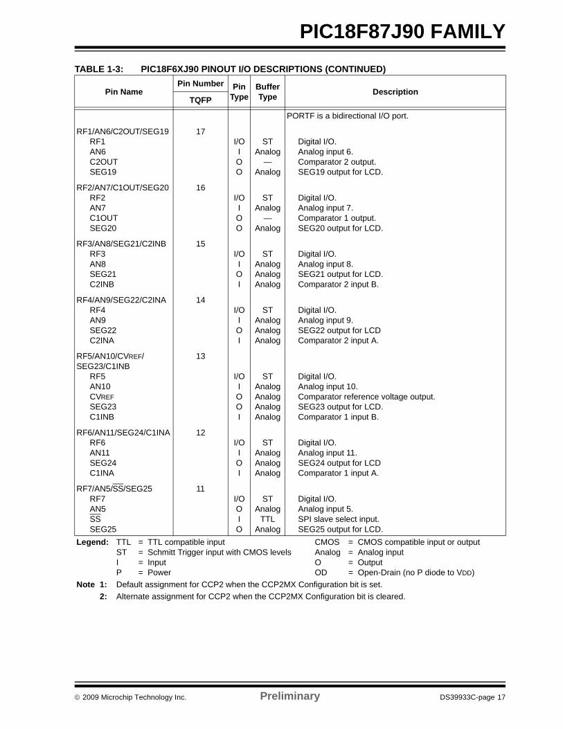
© 2009 Microchip Technology Inc. Preliminary DS39933C-page 17
PIC18F87J90 FAMILY
PORTF is a bidirectional I/O port.
RF1/AN6/C2OUT/SEG19RF1AN6C2OUTSEG19
17I/OIOO
STAnalog
—Analog
Digital I/O.Analog input 6.Comparator 2 output.SEG19 output for LCD.
RF2/AN7/C1OUT/SEG20RF2AN7C1OUTSEG20
16I/OIOO
STAnalog
—Analog
Digital I/O.Analog input 7.Comparator 1 output.SEG20 output for LCD.
RF3/AN8/SEG21/C2INBRF3AN8SEG21C2INB
15I/OIOI
STAnalogAnalogAnalog
Digital I/O.Analog input 8.SEG21 output for LCD.Comparator 2 input B.
RF4/AN9/SEG22/C2INARF4AN9SEG22C2INA
14I/OIOI
STAnalogAnalogAnalog
Digital I/O.Analog input 9.SEG22 output for LCDComparator 2 input A.
RF5/AN10/CVREF/SEG23/C1INB
RF5AN10CVREFSEG23C1INB
13
I/OIOOI
STAnalogAnalogAnalogAnalog
Digital I/O.Analog input 10. Comparator reference voltage output.SEG23 output for LCD.Comparator 1 input B.
RF6/AN11/SEG24/C1INARF6AN11SEG24C1INA
12I/OIOI
STAnalogAnalogAnalog
Digital I/O.Analog input 11.SEG24 output for LCDComparator 1 input A.
RF7/AN5/SS/SEG25RF7AN5SSSEG25
11I/OOIO
STAnalog
TTLAnalog
Digital I/O.Analog input 5.SPI slave select input.SEG25 output for LCD.
TABLE 1-3: PIC18F6XJ90 PINOUT I/O DESCRIPTIONS (CONTINUED)
Pin NamePin Number Pin
TypeBufferType Description
TQFP
Legend: TTL = TTL compatible input CMOS = CMOS compatible input or output ST = Schmitt Trigger input with CMOS levels Analog = Analog input I = Input O = Output P = Power OD = Open-Drain (no P diode to VDD)
Note 1: Default assignment for CCP2 when the CCP2MX Configuration bit is set.2: Alternate assignment for CCP2 when the CCP2MX Configuration bit is cleared.
PIC18F87J90 FAMILY
DS39933C-page 18 Preliminary © 2009 Microchip Technology Inc.
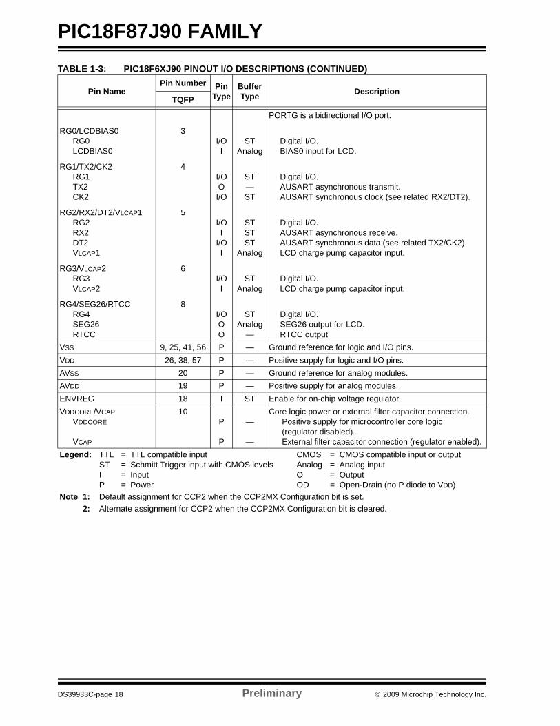
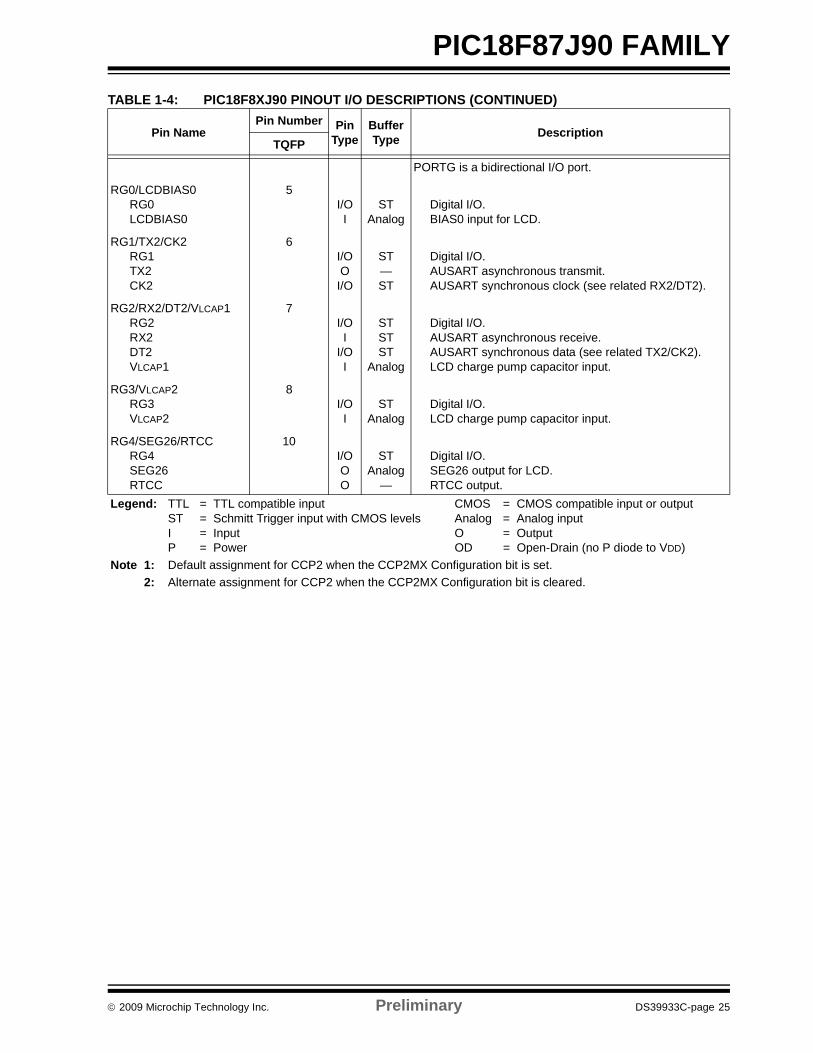
PORTG is a bidirectional I/O port.
RG0/LCDBIAS0RG0LCDBIAS0
3I/OI
STAnalog
Digital I/O.BIAS0 input for LCD.
RG1/TX2/CK2RG1TX2CK2
4I/OOI/O
ST—ST
Digital I/O.AUSART asynchronous transmit. AUSART synchronous clock (see related RX2/DT2).
RG2/RX2/DT2/VLCAP1RG2RX2DT2VLCAP1
5I/OI
I/OI
STSTST
Analog
Digital I/O.AUSART asynchronous receive.AUSART synchronous data (see related TX2/CK2).LCD charge pump capacitor input.
RG3/VLCAP2RG3VLCAP2
6I/OI
STAnalog
Digital I/O.LCD charge pump capacitor input.
RG4/SEG26/RTCCRG4SEG26RTCC
8I/OOO
STAnalog
—
Digital I/O.SEG26 output for LCD.RTCC output
VSS 9, 25, 41, 56 P — Ground reference for logic and I/O pins.VDD 26, 38, 57 P — Positive supply for logic and I/O pins.AVSS 20 P — Ground reference for analog modules.AVDD 19 P — Positive supply for analog modules.ENVREG 18 I ST Enable for on-chip voltage regulator.VDDCORE/VCAP
VDDCORE
VCAP
10P
P
—
—
Core logic power or external filter capacitor connection.Positive supply for microcontroller core logic (regulator disabled).External filter capacitor connection (regulator enabled).
TABLE 1-3: PIC18F6XJ90 PINOUT I/O DESCRIPTIONS (CONTINUED)
Pin NamePin Number Pin
TypeBufferType Description
TQFP
Legend: TTL = TTL compatible input CMOS = CMOS compatible input or output ST = Schmitt Trigger input with CMOS levels Analog = Analog input I = Input O = Output P = Power OD = Open-Drain (no P diode to VDD)
Note 1: Default assignment for CCP2 when the CCP2MX Configuration bit is set.2: Alternate assignment for CCP2 when the CCP2MX Configuration bit is cleared.
© 2009 Microchip Technology Inc. Preliminary DS39933C-page 19
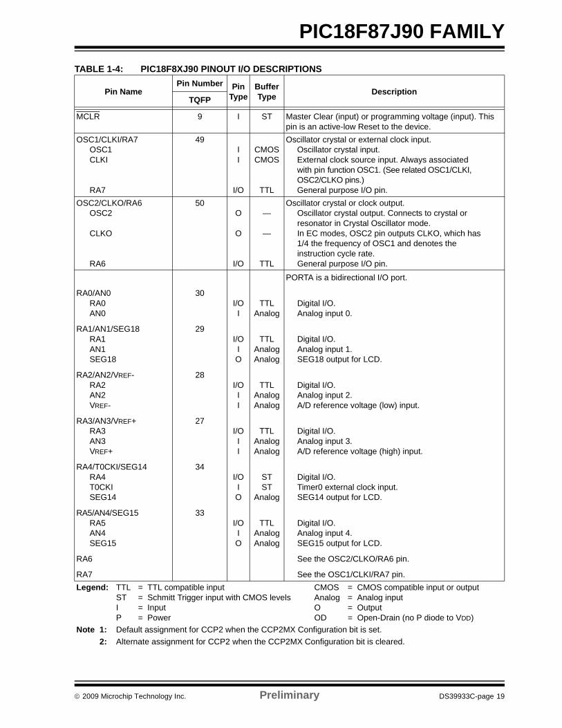
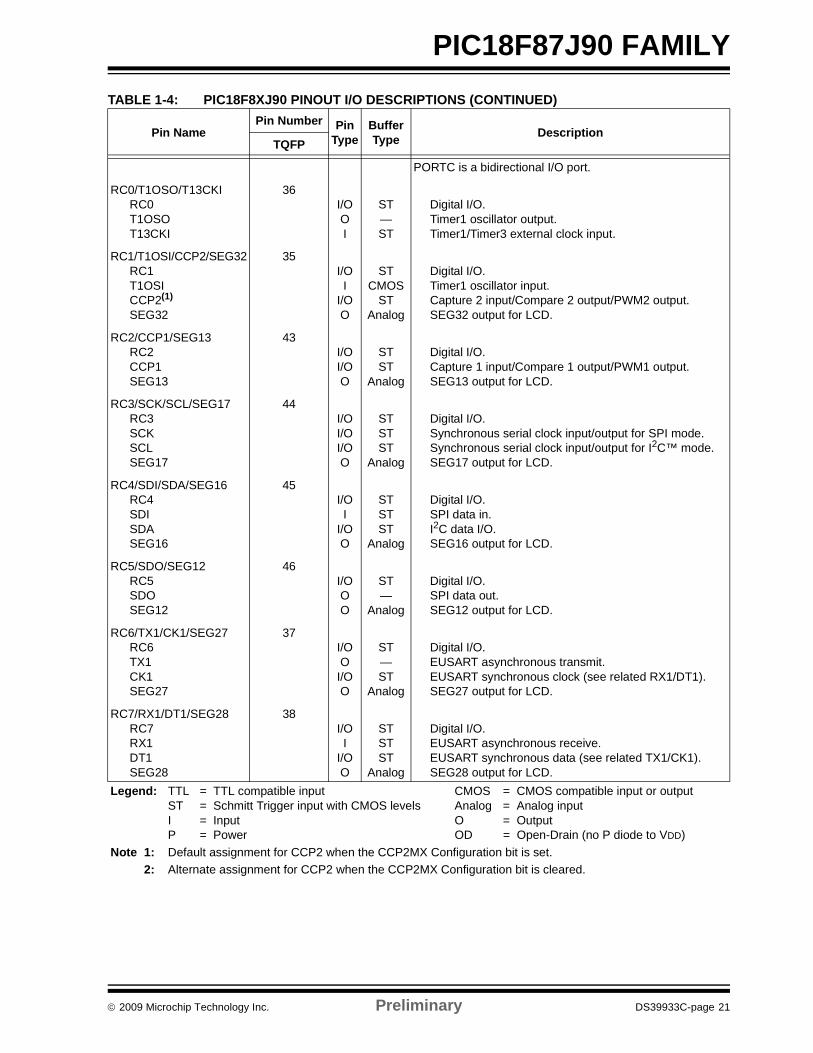
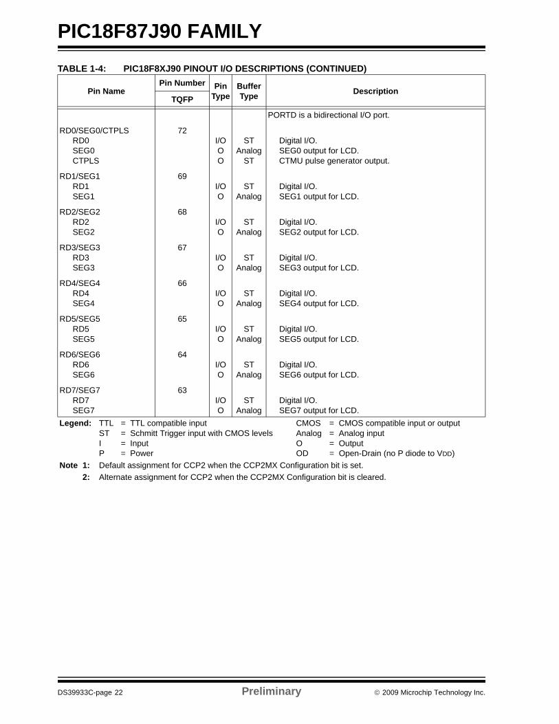
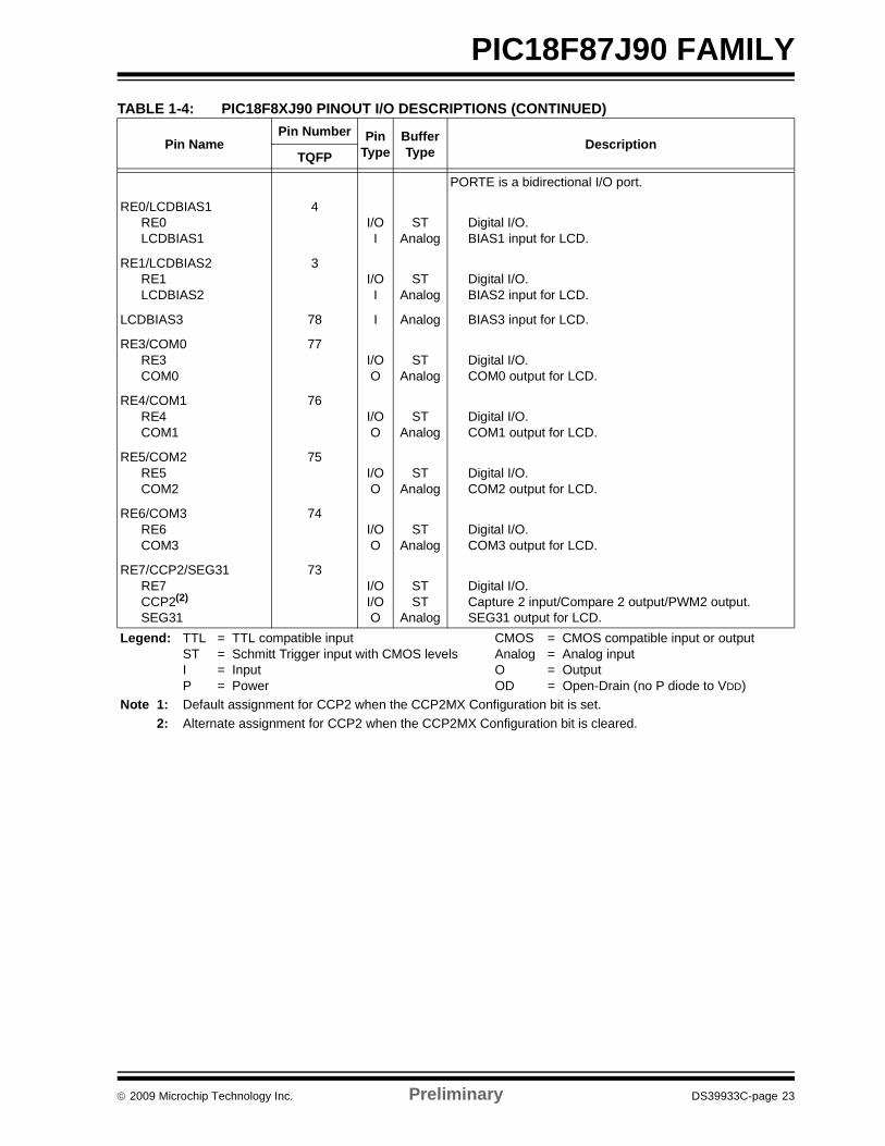
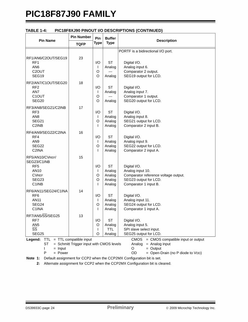
PIC18F87J90 FAMILYTABLE 1-4: PIC18F8XJ90 PINOUT I/O DESCRIPTIONS
Pin NamePin Number Pin
TypeBufferType Description
TQFP
MCLR 9 I ST Master Clear (input) or programming voltage (input). This pin is an active-low Reset to the device.
OSC1/CLKI/RA7OSC1CLKI
RA7
49II
I/O
CMOSCMOS
TTL
Oscillator crystal or external clock input.Oscillator crystal input. External clock source input. Always associated with pin function OSC1. (See related OSC1/CLKI, OSC2/CLKO pins.)General purpose I/O pin.
OSC2/CLKO/RA6OSC2
CLKO
RA6
50O
O
I/O
—
—
TTL
Oscillator crystal or clock output.Oscillator crystal output. Connects to crystal or resonator in Crystal Oscillator mode.In EC modes, OSC2 pin outputs CLKO, which has 1/4 the frequency of OSC1 and denotes theinstruction cycle rate. General purpose I/O pin.
PORTA is a bidirectional I/O port.
RA0/AN0RA0AN0
30I/OI
TTLAnalog
Digital I/O.Analog input 0.
RA1/AN1/SEG18RA1AN1SEG18
29I/OIO
TTLAnalogAnalog
Digital I/O.Analog input 1.SEG18 output for LCD.
RA2/AN2/VREF-RA2AN2VREF-
28I/OII
TTLAnalogAnalog
Digital I/O.Analog input 2.A/D reference voltage (low) input.
RA3/AN3/VREF+RA3AN3VREF+
27I/OII
TTLAnalogAnalog
Digital I/O.Analog input 3.A/D reference voltage (high) input.
RA4/T0CKI/SEG14RA4T0CKISEG14
34I/OIO
STST
Analog
Digital I/O.Timer0 external clock input.SEG14 output for LCD.
RA5/AN4/SEG15RA5AN4SEG15
33I/OIO
TTLAnalogAnalog
Digital I/O.Analog input 4. SEG15 output for LCD.
RA6 See the OSC2/CLKO/RA6 pin.
RA7 See the OSC1/CLKI/RA7 pin.Legend: TTL = TTL compatible input CMOS = CMOS compatible input or output
ST = Schmitt Trigger input with CMOS levels Analog = Analog input I = Input O = Output P = Power OD = Open-Drain (no P diode to VDD)
Note 1: Default assignment for CCP2 when the CCP2MX Configuration bit is set.2: Alternate assignment for CCP2 when the CCP2MX Configuration bit is cleared.
PIC18F87J90 FAMILY
DS39933C-page 20 Preliminary © 2009 Microchip Technology Inc.
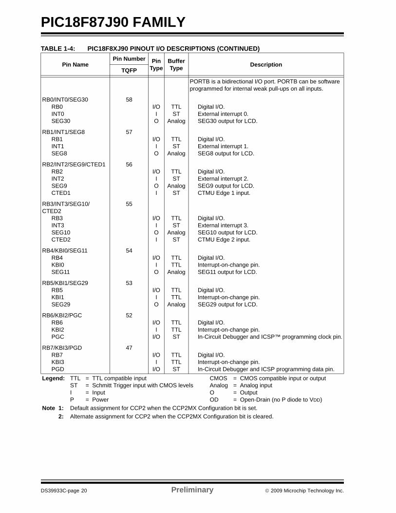
PORTB is a bidirectional I/O port. PORTB can be software programmed for internal weak pull-ups on all inputs.
RB0/INT0/SEG30RB0INT0SEG30
58I/OIO
TTLST
Analog
Digital I/O.External interrupt 0.SEG30 output for LCD.
RB1/INT1/SEG8RB1INT1SEG8
57I/OIO
TTLST
Analog
Digital I/O.External interrupt 1.SEG8 output for LCD.
RB2/INT2/SEG9/CTED1RB2INT2SEG9CTED1
56I/OIOI
TTLST
AnalogST
Digital I/O.External interrupt 2.SEG9 output for LCD.CTMU Edge 1 input.
RB3/INT3/SEG10/CTED2
RB3INT3SEG10CTED2
55
I/OIOI
TTLST
AnalogST
Digital I/O.External interrupt 3.SEG10 output for LCD.CTMU Edge 2 input.
RB4/KBI0/SEG11RB4KBI0SEG11
54I/OIO
TTLTTL
Analog
Digital I/O.Interrupt-on-change pin.SEG11 output for LCD.
RB5/KBI1/SEG29RB5KBI1SEG29
53I/OIO
TTLTTL
Analog
Digital I/O.Interrupt-on-change pin.SEG29 output for LCD.
RB6/KBI2/PGCRB6KBI2PGC
52I/OI
I/O
TTLTTLST
Digital I/O.Interrupt-on-change pin. In-Circuit Debugger and ICSP™ programming clock pin.
RB7/KBI3/PGDRB7KBI3PGD
47I/OI
I/O
TTLTTLST
Digital I/O.Interrupt-on-change pin. In-Circuit Debugger and ICSP programming data pin.
TABLE 1-4: PIC18F8XJ90 PINOUT I/O DESCRIPTIONS (CONTINUED)
Pin NamePin Number Pin
TypeBufferType Description
TQFP
Legend: TTL = TTL compatible input CMOS = CMOS compatible input or output ST = Schmitt Trigger input with CMOS levels Analog = Analog input I = Input O = Output P = Power OD = Open-Drain (no P diode to VDD)
Note 1: Default assignment for CCP2 when the CCP2MX Configuration bit is set.2: Alternate assignment for CCP2 when the CCP2MX Configuration bit is cleared.
© 2009 Microchip Technology Inc. Preliminary DS39933C-page 21
PIC18F87J90 FAMILY
PORTC is a bidirectional I/O port.
RC0/T1OSO/T13CKIRC0T1OSOT13CKI
36I/OOI
ST—ST
Digital I/O.Timer1 oscillator output. Timer1/Timer3 external clock input.
RC1/T1OSI/CCP2/SEG32RC1T1OSICCP2(1)
SEG32
35I/OI
I/OO
STCMOS
STAnalog
Digital I/O.Timer1 oscillator input.Capture 2 input/Compare 2 output/PWM2 output.SEG32 output for LCD.
RC2/CCP1/SEG13RC2CCP1SEG13
43I/OI/OO
STST
Analog
Digital I/O.Capture 1 input/Compare 1 output/PWM1 output.SEG13 output for LCD.
RC3/SCK/SCL/SEG17RC3SCKSCLSEG17
44I/OI/OI/OO
STSTST
Analog
Digital I/O.Synchronous serial clock input/output for SPI mode.Synchronous serial clock input/output for I2C™ mode.SEG17 output for LCD.
RC4/SDI/SDA/SEG16RC4SDISDASEG16
45I/OI
I/OO
STSTST
Analog
Digital I/O.SPI data in.I2C data I/O.SEG16 output for LCD.
RC5/SDO/SEG12RC5SDOSEG12
46I/OOO
ST—
Analog
Digital I/O.SPI data out.SEG12 output for LCD.
RC6/TX1/CK1/SEG27RC6TX1CK1SEG27
37I/OO
I/OO
ST—ST
Analog
Digital I/O.EUSART asynchronous transmit. EUSART synchronous clock (see related RX1/DT1).SEG27 output for LCD.
RC7/RX1/DT1/SEG28RC7RX1DT1SEG28
38I/OI
I/OO
STSTST
Analog
Digital I/O.EUSART asynchronous receive.EUSART synchronous data (see related TX1/CK1).SEG28 output for LCD.
TABLE 1-4: PIC18F8XJ90 PINOUT I/O DESCRIPTIONS (CONTINUED)
Pin NamePin Number Pin
TypeBufferType Description
TQFP
Legend: TTL = TTL compatible input CMOS = CMOS compatible input or output ST = Schmitt Trigger input with CMOS levels Analog = Analog input I = Input O = Output P = Power OD = Open-Drain (no P diode to VDD)
Note 1: Default assignment for CCP2 when the CCP2MX Configuration bit is set.2: Alternate assignment for CCP2 when the CCP2MX Configuration bit is cleared.
PIC18F87J90 FAMILY
DS39933C-page 22 Preliminary © 2009 Microchip Technology Inc.
PORTD is a bidirectional I/O port.
RD0/SEG0/CTPLSRD0SEG0CTPLS
72I/OOO
STAnalog
ST
Digital I/O.SEG0 output for LCD.CTMU pulse generator output.
RD1/SEG1RD1SEG1
69I/OO
STAnalog
Digital I/O.SEG1 output for LCD.
RD2/SEG2RD2SEG2
68I/OO
STAnalog
Digital I/O.SEG2 output for LCD.
RD3/SEG3RD3SEG3
67I/OO
STAnalog
Digital I/O.SEG3 output for LCD.
RD4/SEG4RD4SEG4
66I/OO
STAnalog
Digital I/O.SEG4 output for LCD.
RD5/SEG5RD5SEG5
65I/OO
STAnalog
Digital I/O.SEG5 output for LCD.
RD6/SEG6RD6SEG6
64I/OO
STAnalog
Digital I/O.SEG6 output for LCD.
RD7/SEG7RD7SEG7
63I/OO
STAnalog
Digital I/O.SEG7 output for LCD.
TABLE 1-4: PIC18F8XJ90 PINOUT I/O DESCRIPTIONS (CONTINUED)
Pin NamePin Number Pin
TypeBufferType Description
TQFP
Legend: TTL = TTL compatible input CMOS = CMOS compatible input or output ST = Schmitt Trigger input with CMOS levels Analog = Analog input I = Input O = Output P = Power OD = Open-Drain (no P diode to VDD)
Note 1: Default assignment for CCP2 when the CCP2MX Configuration bit is set.2: Alternate assignment for CCP2 when the CCP2MX Configuration bit is cleared.
© 2009 Microchip Technology Inc. Preliminary DS39933C-page 23
PIC18F87J90 FAMILY
PORTE is a bidirectional I/O port.
RE0/LCDBIAS1RE0LCDBIAS1
4I/OI
STAnalog
Digital I/O.BIAS1 input for LCD.
RE1/LCDBIAS2RE1LCDBIAS2
3I/OI
STAnalog
Digital I/O.BIAS2 input for LCD.
LCDBIAS3 78 I Analog BIAS3 input for LCD.
RE3/COM0RE3COM0
77I/OO
STAnalog
Digital I/O.COM0 output for LCD.
RE4/COM1RE4COM1
76I/OO
STAnalog
Digital I/O.COM1 output for LCD.
RE5/COM2RE5COM2
75I/OO
STAnalog
Digital I/O.COM2 output for LCD.
RE6/COM3RE6COM3
74I/OO
STAnalog
Digital I/O.COM3 output for LCD.
RE7/CCP2/SEG31RE7CCP2(2)
SEG31
73I/OI/OO
STST
Analog
Digital I/O.Capture 2 input/Compare 2 output/PWM2 output.SEG31 output for LCD.
TABLE 1-4: PIC18F8XJ90 PINOUT I/O DESCRIPTIONS (CONTINUED)
Pin NamePin Number Pin
TypeBufferType Description
TQFP
Legend: TTL = TTL compatible input CMOS = CMOS compatible input or output ST = Schmitt Trigger input with CMOS levels Analog = Analog input I = Input O = Output P = Power OD = Open-Drain (no P diode to VDD)
Note 1: Default assignment for CCP2 when the CCP2MX Configuration bit is set.2: Alternate assignment for CCP2 when the CCP2MX Configuration bit is cleared.
PIC18F87J90 FAMILY
DS39933C-page 24 Preliminary © 2009 Microchip Technology Inc.
PORTF is a bidirectional I/O port.
RF1/AN6/C2OUT/SEG19RF1AN6C2OUTSEG19
23I/OIOO
STAnalog
—Analog
Digital I/O.Analog input 6.Comparator 2 output.SEG19 output for LCD.
RF2/AN7/C1OUT/SEG20RF2AN7C1OUTSEG20
18I/OIOO
STAnalog
—Analog
Digital I/O.Analog input 7.Comparator 1 output.SEG20 output for LCD.
RF3/AN8/SEG21/C2INBRF3AN8SEG21C2INB
17I/OIOI
STAnalogAnalogAnalog
Digital I/O.Analog input 8.SEG21 output for LCD.Comparator 2 input B.
RF4/AN9/SEG22/C2INARF4AN9SEG22C2INA
16I/OIOI
STAnalogAnalogAnalog
Digital I/O.Analog input 9.SEG22 output for LCD.Comparator 2 input A.
RF5/AN10/CVREF/SEG23/C1INB
RF5AN10CVREFSEG23C1INB
15
I/OIOOI
STAnalogAnalogAnalogAnalog
Digital I/O.Analog input 10. Comparator reference voltage output.SEG23 output for LCD.Comparator 1 input B.
RF6/AN11/SEG24/C1INARF6AN11SEG24C1INA
14I/OIOI
STAnalogAnalogAnalog
Digital I/O.Analog input 11.SEG24 output for LCD.Comparator 1 input A.
RF7/AN5/SS/SEG25RF7AN5SSSEG25
13I/OOIO
STAnalog
TTLAnalog
Digital I/O.Analog input 5.SPI slave select input.SEG25 output for LCD.
TABLE 1-4: PIC18F8XJ90 PINOUT I/O DESCRIPTIONS (CONTINUED)
Pin NamePin Number Pin
TypeBufferType Description
TQFP
Legend: TTL = TTL compatible input CMOS = CMOS compatible input or output ST = Schmitt Trigger input with CMOS levels Analog = Analog input I = Input O = Output P = Power OD = Open-Drain (no P diode to VDD)
Note 1: Default assignment for CCP2 when the CCP2MX Configuration bit is set.2: Alternate assignment for CCP2 when the CCP2MX Configuration bit is cleared.
© 2009 Microchip Technology Inc. Preliminary DS39933C-page 25
PIC18F87J90 FAMILY
PORTG is a bidirectional I/O port.
RG0/LCDBIAS0RG0LCDBIAS0
5I/OI
STAnalog
Digital I/O.BIAS0 input for LCD.
RG1/TX2/CK2RG1TX2CK2
6I/OO
I/O
ST—ST
Digital I/O.AUSART asynchronous transmit. AUSART synchronous clock (see related RX2/DT2).
RG2/RX2/DT2/VLCAP1RG2RX2DT2VLCAP1
7I/OI
I/OI
STSTST
Analog
Digital I/O.AUSART asynchronous receive.AUSART synchronous data (see related TX2/CK2).LCD charge pump capacitor input.
RG3/VLCAP2RG3VLCAP2
8I/OI
STAnalog
Digital I/O.LCD charge pump capacitor input.
RG4/SEG26/RTCCRG4SEG26RTCC
10I/OOO
STAnalog
—
Digital I/O.SEG26 output for LCD.RTCC output.
TABLE 1-4: PIC18F8XJ90 PINOUT I/O DESCRIPTIONS (CONTINUED)
Pin NamePin Number Pin
TypeBufferType Description
TQFP
Legend: TTL = TTL compatible input CMOS = CMOS compatible input or output ST = Schmitt Trigger input with CMOS levels Analog = Analog input I = Input O = Output P = Power OD = Open-Drain (no P diode to VDD)
Note 1: Default assignment for CCP2 when the CCP2MX Configuration bit is set.2: Alternate assignment for CCP2 when the CCP2MX Configuration bit is cleared.
PIC18F87J90 FAMILY
DS39933C-page 26 Preliminary © 2009 Microchip Technology Inc.
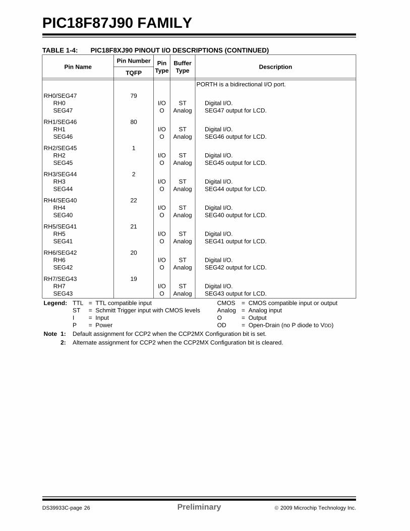
PORTH is a bidirectional I/O port.
RH0/SEG47RH0SEG47
79I/OO
STAnalog
Digital I/O.SEG47 output for LCD.
RH1/SEG46RH1SEG46
80I/OO
STAnalog
Digital I/O.SEG46 output for LCD.
RH2/SEG45RH2SEG45
1I/OO
STAnalog
Digital I/O.SEG45 output for LCD.
RH3/SEG44RH3SEG44
2I/OO
STAnalog
Digital I/O.SEG44 output for LCD.
RH4/SEG40RH4SEG40
22I/OO
STAnalog
Digital I/O.SEG40 output for LCD.
RH5/SEG41RH5SEG41
21I/OO
STAnalog
Digital I/O.SEG41 output for LCD.
RH6/SEG42RH6SEG42
20I/OO
STAnalog
Digital I/O.SEG42 output for LCD.
RH7/SEG43RH7SEG43
19I/OO
STAnalog
Digital I/O.SEG43 output for LCD.
TABLE 1-4: PIC18F8XJ90 PINOUT I/O DESCRIPTIONS (CONTINUED)
Pin NamePin Number Pin
TypeBufferType Description
TQFP
Legend: TTL = TTL compatible input CMOS = CMOS compatible input or output ST = Schmitt Trigger input with CMOS levels Analog = Analog input I = Input O = Output P = Power OD = Open-Drain (no P diode to VDD)
Note 1: Default assignment for CCP2 when the CCP2MX Configuration bit is set.2: Alternate assignment for CCP2 when the CCP2MX Configuration bit is cleared.
© 2009 Microchip Technology Inc. Preliminary DS39933C-page 27
PIC18F87J90 FAMILY
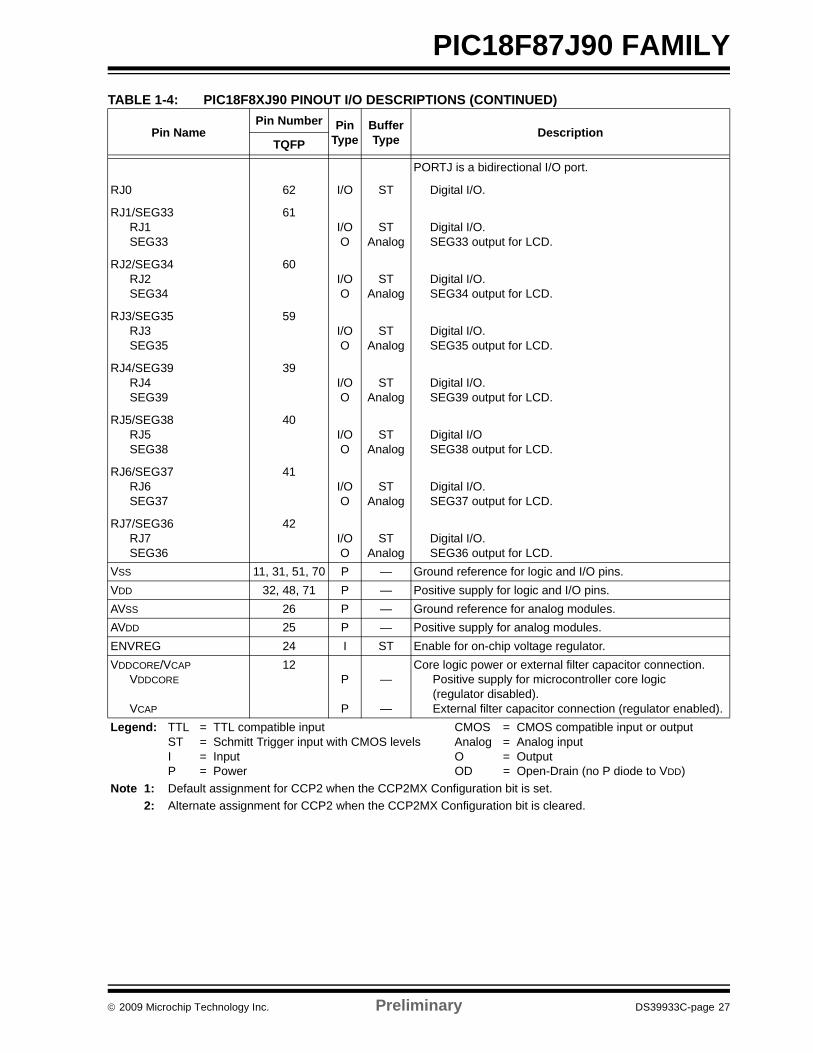
PORTJ is a bidirectional I/O port.
RJ0 62 I/O ST Digital I/O.
RJ1/SEG33RJ1SEG33
61I/OO
STAnalog
Digital I/O.SEG33 output for LCD.
RJ2/SEG34RJ2SEG34
60I/OO
STAnalog
Digital I/O.SEG34 output for LCD.
RJ3/SEG35RJ3SEG35
59I/OO
STAnalog
Digital I/O.SEG35 output for LCD.
RJ4/SEG39RJ4SEG39
39I/OO
STAnalog
Digital I/O.SEG39 output for LCD.
RJ5/SEG38RJ5SEG38
40I/OO
STAnalog
Digital I/OSEG38 output for LCD.
RJ6/SEG37RJ6SEG37
41I/OO
STAnalog
Digital I/O.SEG37 output for LCD.
RJ7/SEG36RJ7SEG36
42I/OO
STAnalog
Digital I/O.SEG36 output for LCD.
VSS 11, 31, 51, 70 P — Ground reference for logic and I/O pins.VDD 32, 48, 71 P — Positive supply for logic and I/O pins.AVSS 26 P — Ground reference for analog modules.AVDD 25 P — Positive supply for analog modules.ENVREG 24 I ST Enable for on-chip voltage regulator.VDDCORE/VCAP
VDDCORE
VCAP
12P
P
—
—
Core logic power or external filter capacitor connection.Positive supply for microcontroller core logic (regulator disabled).External filter capacitor connection (regulator enabled).
TABLE 1-4: PIC18F8XJ90 PINOUT I/O DESCRIPTIONS (CONTINUED)
Pin NamePin Number Pin
TypeBufferType Description
TQFP
Legend: TTL = TTL compatible input CMOS = CMOS compatible input or output ST = Schmitt Trigger input with CMOS levels Analog = Analog input I = Input O = Output P = Power OD = Open-Drain (no P diode to VDD)
Note 1: Default assignment for CCP2 when the CCP2MX Configuration bit is set.2: Alternate assignment for CCP2 when the CCP2MX Configuration bit is cleared.

PIC18F87J90 FAMILY
DS39933C-page 28 Preliminary © 2009 Microchip Technology Inc.
NOTES:
© 2009 Microchip Technology Inc. Preliminary DS39933C-page 29
PIC18F87J90 FAMILY
2.0 OSCILLATOR CONFIGURATIONS
2.1 Oscillator TypesThe PIC18F87J90 family of devices can be operated ineight different oscillator modes:
1. ECPLL OSC1/OSC2 as primary; ECPLLoscillator with PLL enabled, CLKO onRA6
2. EC OSC1/OSC2 as primary; externalclock with FOSC/4 output
3. HSPLL OSC1/OSC2 as primary; high-speedcrystal/resonator with software PLLcontrol
4. HS OSC1/OSC2 as primary; high-speedcrystal/resonator
5. INTPLL1 Internal oscillator block with softwarePLL control, FOSC/4 output on RA6and I/O on RA7
6. INTIO1 Internal oscillator block with FOSC/4output on RA6 and I/O on RA7
7. INTPLL2 Internal oscillator block with softwarePLL control and I/O on RA6 and RA7
8. INTIO2 Internal oscillator block with I/O onRA6 and RA7
All of these modes are selected by the user byprogramming the FOSC<2:0> Configuration bits.
In addition, PIC18F87J90 family devices can switchbetween different clock sources, either under softwarecontrol or automatically under certain conditions. Thisallows for additional power savings by managingdevice clock speed in real time without resetting theapplication.
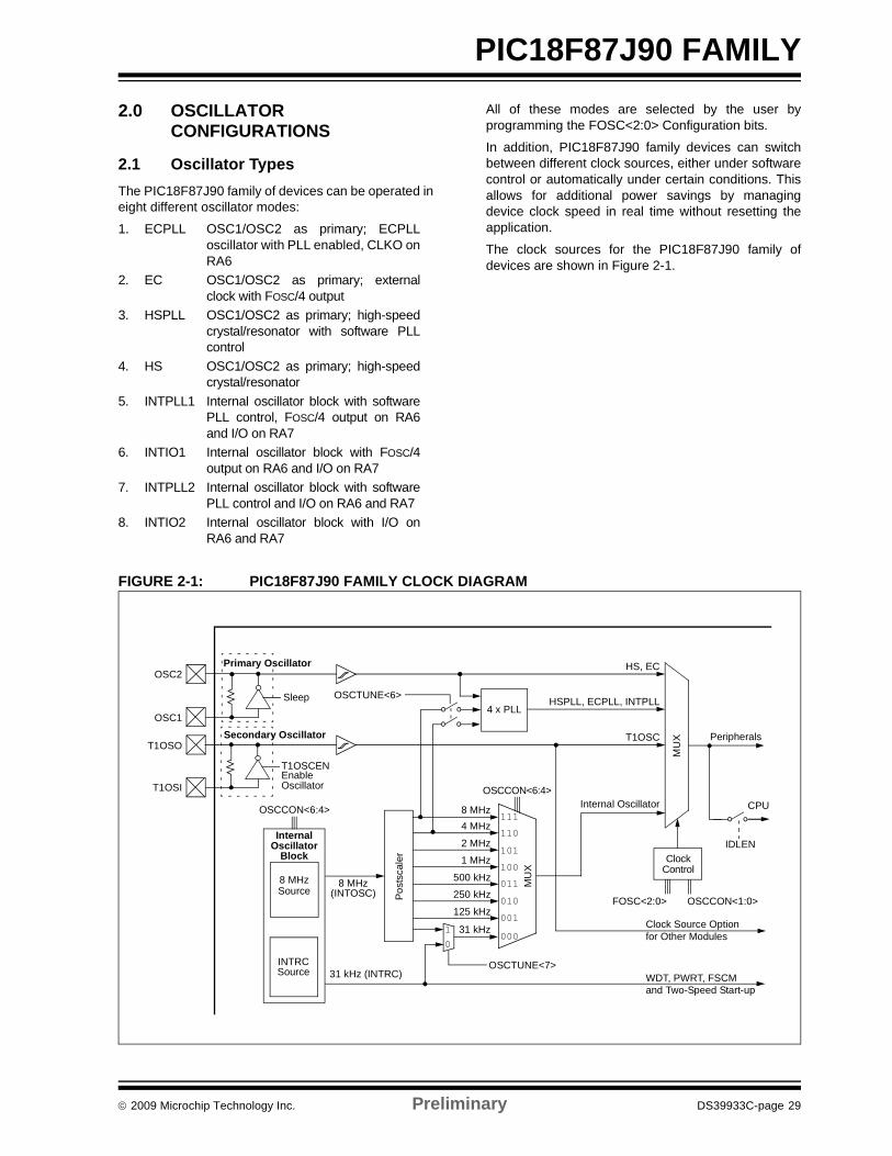
The clock sources for the PIC18F87J90 family ofdevices are shown in Figure 2-1.
FIGURE 2-1: PIC18F87J90 FAMILY CLOCK DIAGRAM
4 x PLL
FOSC<2:0>
Secondary Oscillator
T1OSCENEnableOscillator
T1OSO
T1OSI
Clock Source Option for Other Modules
OSC1
OSC2
Sleep HSPLL, ECPLL, INTPLL
HS, EC
T1OSC
CPU
Peripherals
IDLEN
Post
scal
er
MU
X
MU
X
8 MHz4 MHz
2 MHz
1 MHz
500 kHz
125 kHz
250 kHz
OSCCON<6:4>
111
110
101
100
011
010
001
00031 kHz
INTRCSource
InternalOscillator
Block
WDT, PWRT, FSCM
8 MHz
Internal Oscillator
(INTOSC)
OSCCON<6:4>
ClockControl
OSCCON<1:0> Source8 MHz
31 kHz (INTRC)
0
1
OSCTUNE<7>
and Two-Speed Start-up
Primary Oscillator
OSCTUNE<6>
PIC18F87J90 FAMILY
DS39933C-page 30 Preliminary © 2009 Microchip Technology Inc.
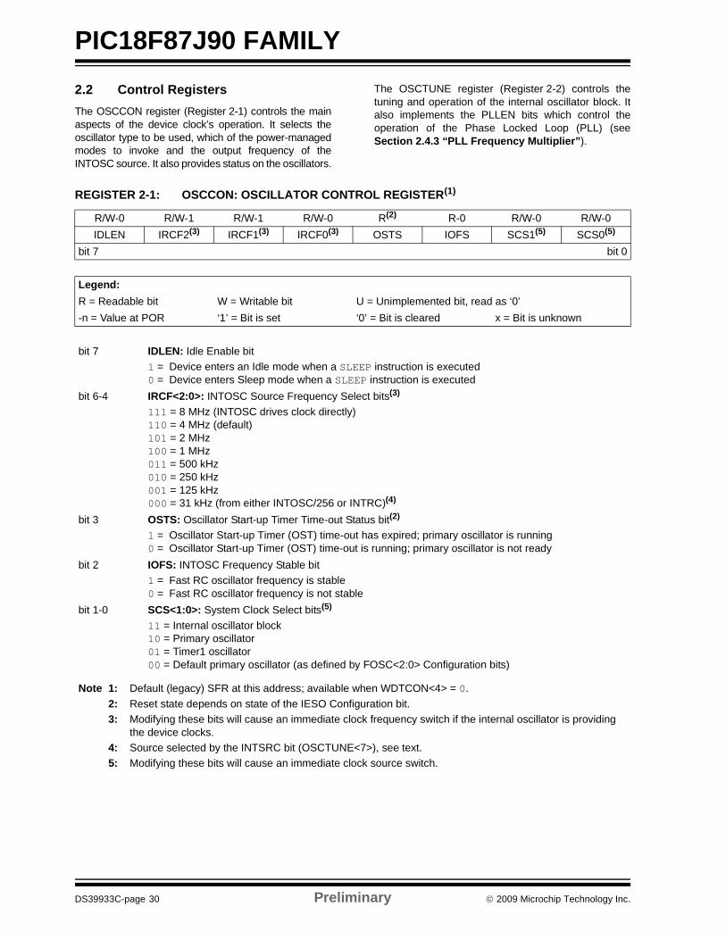
2.2 Control RegistersThe OSCCON register (Register 2-1) controls the mainaspects of the device clock’s operation. It selects theoscillator type to be used, which of the power-managedmodes to invoke and the output frequency of theINTOSC source. It also provides status on the oscillators.
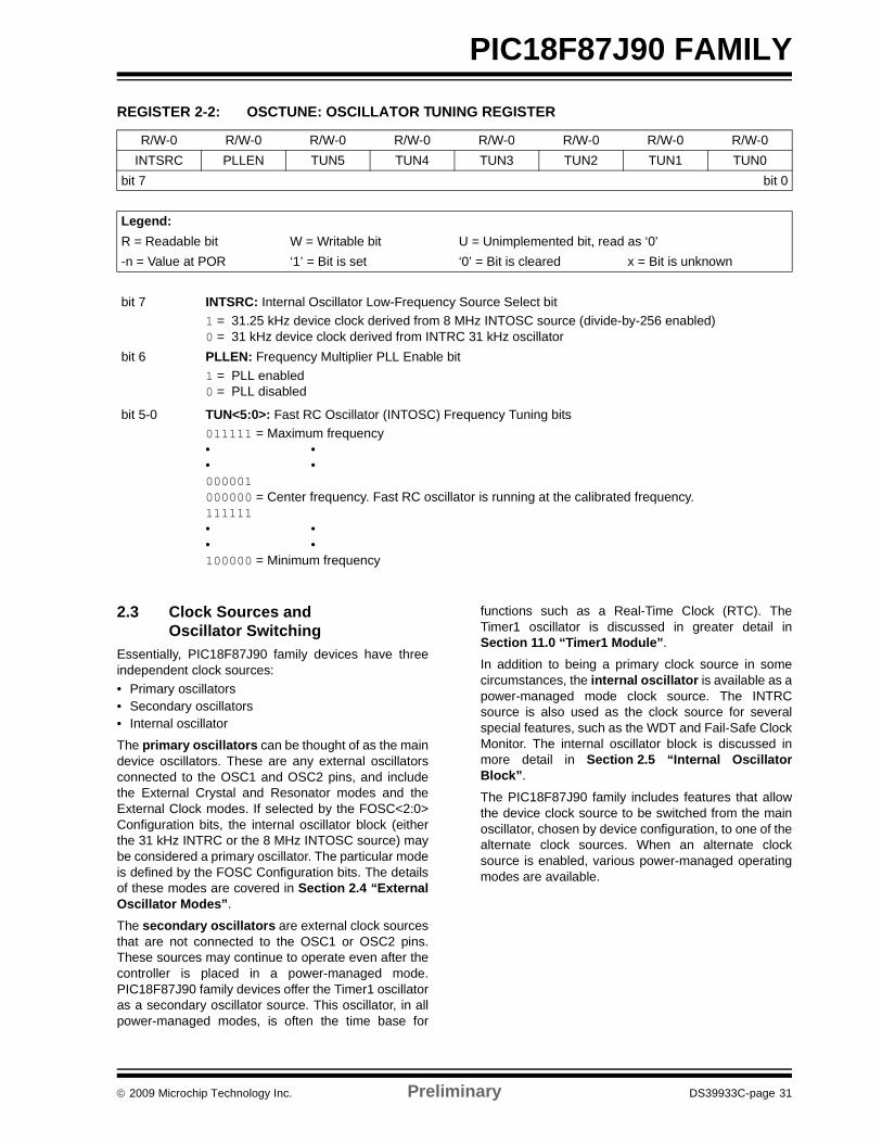
The OSCTUNE register (Register 2-2) controls thetuning and operation of the internal oscillator block. Italso implements the PLLEN bits which control theoperation of the Phase Locked Loop (PLL) (seeSection 2.4.3 “PLL Frequency Multiplier”).
REGISTER 2-1: OSCCON: OSCILLATOR CONTROL REGISTER(1)
R/W-0 R/W-1 R/W-1 R/W-0 R(2) R-0 R/W-0 R/W-0IDLEN IRCF2(3) IRCF1(3) IRCF0(3) OSTS IOFS SCS1(5) SCS0(5)
bit 7 bit 0
Legend:R = Readable bit W = Writable bit U = Unimplemented bit, read as ‘0’-n = Value at POR ‘1’ = Bit is set ‘0’ = Bit is cleared x = Bit is unknown
bit 7 IDLEN: Idle Enable bit1 = Device enters an Idle mode when a SLEEP instruction is executed0 = Device enters Sleep mode when a SLEEP instruction is executed
bit 6-4 IRCF<2:0>: INTOSC Source Frequency Select bits(3)
111 = 8 MHz (INTOSC drives clock directly)110 = 4 MHz (default)101 = 2 MHz 100 = 1 MHz011 = 500 kHz 010 = 250 kHz001 = 125 kHz000 = 31 kHz (from either INTOSC/256 or INTRC)(4)
bit 3 OSTS: Oscillator Start-up Timer Time-out Status bit(2)
1 = Oscillator Start-up Timer (OST) time-out has expired; primary oscillator is running0 = Oscillator Start-up Timer (OST) time-out is running; primary oscillator is not ready
bit 2 IOFS: INTOSC Frequency Stable bit 1 = Fast RC oscillator frequency is stable0 = Fast RC oscillator frequency is not stable
bit 1-0 SCS<1:0>: System Clock Select bits(5)
11 = Internal oscillator block10 = Primary oscillator01 = Timer1 oscillator00 = Default primary oscillator (as defined by FOSC<2:0> Configuration bits)
Note 1: Default (legacy) SFR at this address; available when WDTCON<4> = 0.2: Reset state depends on state of the IESO Configuration bit.3: Modifying these bits will cause an immediate clock frequency switch if the internal oscillator is providing
the device clocks.4: Source selected by the INTSRC bit (OSCTUNE<7>), see text.5: Modifying these bits will cause an immediate clock source switch.
© 2009 Microchip Technology Inc. Preliminary DS39933C-page 31
PIC18F87J90 FAMILY
2.3 Clock Sources and Oscillator Switching
Essentially, PIC18F87J90 family devices have threeindependent clock sources:• Primary oscillators• Secondary oscillators• Internal oscillator
The primary oscillators can be thought of as the maindevice oscillators. These are any external oscillatorsconnected to the OSC1 and OSC2 pins, and includethe External Crystal and Resonator modes and theExternal Clock modes. If selected by the FOSC<2:0>Configuration bits, the internal oscillator block (eitherthe 31 kHz INTRC or the 8 MHz INTOSC source) maybe considered a primary oscillator. The particular modeis defined by the FOSC Configuration bits. The detailsof these modes are covered in Section 2.4 “ExternalOscillator Modes”.
The secondary oscillators are external clock sourcesthat are not connected to the OSC1 or OSC2 pins.These sources may continue to operate even after thecontroller is placed in a power-managed mode.PIC18F87J90 family devices offer the Timer1 oscillatoras a secondary oscillator source. This oscillator, in allpower-managed modes, is often the time base for
functions such as a Real-Time Clock (RTC). TheTimer1 oscillator is discussed in greater detail inSection 11.0 “Timer1 Module”.
In addition to being a primary clock source in somecircumstances, the internal oscillator is available as apower-managed mode clock source. The INTRCsource is also used as the clock source for severalspecial features, such as the WDT and Fail-Safe ClockMonitor. The internal oscillator block is discussed inmore detail in Section 2.5 “Internal OscillatorBlock”.
The PIC18F87J90 family includes features that allowthe device clock source to be switched from the mainoscillator, chosen by device configuration, to one of thealternate clock sources. When an alternate clocksource is enabled, various power-managed operatingmodes are available.
REGISTER 2-2: OSCTUNE: OSCILLATOR TUNING REGISTER
R/W-0 R/W-0 R/W-0 R/W-0 R/W-0 R/W-0 R/W-0 R/W-0 INTSRC PLLEN TUN5 TUN4 TUN3 TUN2 TUN1 TUN0
bit 7 bit 0
Legend:R = Readable bit W = Writable bit U = Unimplemented bit, read as ‘0’-n = Value at POR ‘1’ = Bit is set ‘0’ = Bit is cleared x = Bit is unknown
bit 7 INTSRC: Internal Oscillator Low-Frequency Source Select bit1 = 31.25 kHz device clock derived from 8 MHz INTOSC source (divide-by-256 enabled)0 = 31 kHz device clock derived from INTRC 31 kHz oscillator
bit 6 PLLEN: Frequency Multiplier PLL Enable bit1 = PLL enabled0 = PLL disabled
bit 5-0 TUN<5:0>: Fast RC Oscillator (INTOSC) Frequency Tuning bits011111 = Maximum frequency• •• •000001 000000 = Center frequency. Fast RC oscillator is running at the calibrated frequency.111111 • •• •100000 = Minimum frequency
PIC18F87J90 FAMILY
DS39933C-page 32 Preliminary © 2009 Microchip Technology Inc.
2.3.1 CLOCK SOURCE SELECTIONThe System Clock Select bits, SCS<1:>0(OSCCON<1:0>), select the clock source. The avail-able clock sources are the primary clock defined by theFOSC<2:0> Configuration bits, the secondary clock(Timer1 oscillator) and the internal oscillator. The clocksource changes after one or more of the bits is writtento, following a brief clock transition interval.
The OSTS (OSCCON<3>) and T1RUN (T1CON<6>)bits indicate which clock source is currently providingthe device clock. The OSTS bit indicates that theOscillator Start-up Timer (OST) has timed out and theprimary clock is providing the device clock in primaryclock modes. The T1RUN bit indicates when theTimer1 oscillator is providing the device clock in sec-ondary clock modes. In power-managed modes, onlyone of these bits will be set at any time. If neither ofthese bits is set, the INTRC is providing the clock, orthe internal oscillator has just started and is not yetstable.
The IDLEN bit determines if the device goes into Sleepmode or one of the Idle modes when the SLEEPinstruction is executed.
The use of the flag and control bits in the OSCCONregister is discussed in more detail in Section 3.0“Power-Managed Modes”.
2.3.1.1 System Clock Selection and Device Resets
Since the SCS bits are cleared on all forms of Reset,this means the primary oscillator defined by theFOSC<2:0> Configuration bits is used as the primaryclock source on device Resets. This could either be theinternal oscillator block by itself, or one of the otherprimary clock source (HS, EC, HSPLL, ECPLL1/2 orINTPLL1/2).
In those cases when the internal oscillator block, with-out PLL, is the default clock on Reset, the Fast RCoscillator (INTOSC) will be used as the device clocksource. It will initially start at 1 MHz, the postscalerselection that corresponds to the Reset value of theIRCF<2:0> bits (‘100’).
Regardless of which primary oscillator is selected,INTRC will always be enabled on device power-up. Itserves as the clock source until the device has loadedits configuration values from memory. It is at this pointthat the FOSC Configuration bits are read and theoscillator selection of the operational mode is made.
Note that either the primary clock source, or the internaloscillator, will have two bit setting options for the possiblevalues of the SCS<1:0> bits at any given time.
2.3.2 OSCILLATOR TRANSITIONSPIC18F87J90 family devices contain circuitry toprevent clock “glitches” when switching between clocksources. A short pause in the device clock occurs dur-ing the clock switch. The length of this pause is the sumof two cycles of the old clock source and three to fourcycles of the new clock source. This formula assumesthat the new clock source is stable.
Clock transitions are discussed in greater detail inSection 3.1.2 “Entering Power-Managed Modes”.
Note 1: The Timer1 oscillator must be enabled toselect the secondary clock source. TheTimer1 oscillator is enabled by setting theT1OSCEN bit in the Timer1 Control regis-ter (T1CON<3>). If the Timer1 oscillator isnot enabled, then any attempt to select asecondary clock source when executing aSLEEP instruction will be ignored.
2: It is recommended that the Timer1oscillator be operating and stable beforeexecuting the SLEEP instruction or a verylong delay may occur while the Timer1oscillator starts.
© 2009 Microchip Technology Inc. Preliminary DS39933C-page 33
PIC18F87J90 FAMILY2.4 External Oscillator Modes
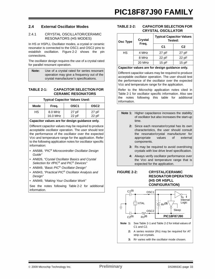
2.4.1 CRYSTAL OSCILLATOR/CERAMIC RESONATORS (HS MODES)
In HS or HSPLL Oscillator modes, a crystal or ceramicresonator is connected to the OSC1 and OSC2 pins toestablish oscillation. Figure 2-2 shows the pinconnections.
The oscillator design requires the use of a crystal ratedfor parallel resonant operation.
TABLE 2-1: CAPACITOR SELECTION FOR CERAMIC RESONATORS
TABLE 2-2: CAPACITOR SELECTION FOR CRYSTAL OSCILLATOR
FIGURE 2-2: CRYSTAL/CERAMIC RESONATOR OPERATION (HS OR HSPLL CONFIGURATION)
Note: Use of a crystal rated for series resonantoperation may give a frequency out of thecrystal manufacturer’s specifications.
Typical Capacitor Values Used:
Mode Freq. OSC1 OSC2
HS 8.0 MHz16.0 MHz
27 pF22 pF
27 pF22 pF
Capacitor values are for design guidance only. Different capacitor values may be required to produceacceptable oscillator operation. The user should testthe performance of the oscillator over the expectedVDD and temperature range for the application. Referto the following application notes for oscillator specificinformation:
• AN588, “PIC® Microcontroller Oscillator Design Guide”
• AN826, “Crystal Oscillator Basics and Crystal Selection for rfPIC® and PIC® Devices”
• AN849, “Basic PIC® Oscillator Design”• AN943, “Practical PIC® Oscillator Analysis and
Design”• AN949, “Making Your Oscillator Work”
See the notes following Table 2-2 for additionalinformation.
Osc Type Crystal Freq.
Typical Capacitor Values Tested:
C1 C2
HS 4 MHz 27 pF 27 pF8 MHz 22 pF 22 pF
20 MHz 15 pF 15 pFCapacitor values are for design guidance only. Different capacitor values may be required to produceacceptable oscillator operation. The user should testthe performance of the oscillator over the expectedVDD and temperature range for the application.
Refer to the Microchip application notes cited inTable 2-1 for oscillator specific information. Also seethe notes following this table for additionalinformation.
Note 1: Higher capacitance increases the stabilityof oscillator but also increases the start-uptime.
2: Since each resonator/crystal has its owncharacteristics, the user should consultthe resonator/crystal manufacturer forappropriate values of externalcomponents.
3: Rs may be required to avoid overdrivingcrystals with low drive level specification.
4: Always verify oscillator performance overthe VDD and temperature range that isexpected for the application.
Note 1: See Table 2-1 and Table 2-2 for initial values ofC1 and C2.
2: A series resistor (RS) may be required for ATstrip cut crystals.
3: RF varies with the oscillator mode chosen.
C1(1)
C2(1)
XTAL
OSC2
OSC1
RF(3)
Sleep
To
Logic
RS(2)
Internal
PIC18F87J90
PIC18F87J90 FAMILY
DS39933C-page 34 Preliminary © 2009 Microchip Technology Inc.
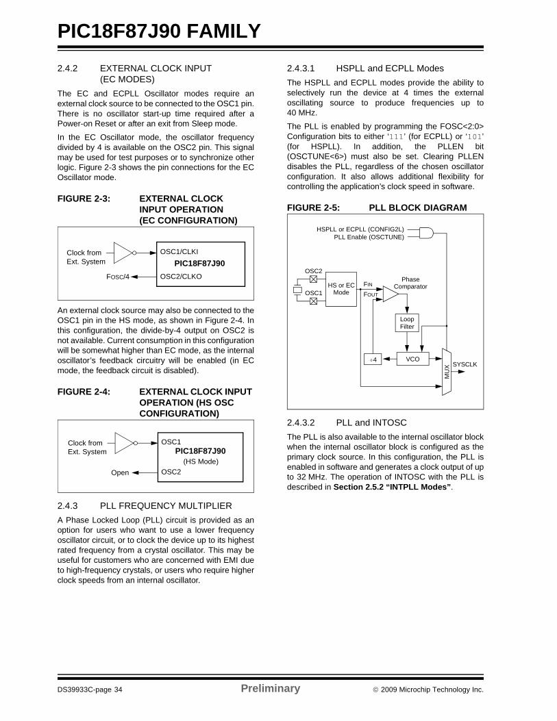
2.4.2 EXTERNAL CLOCK INPUT (EC MODES)
The EC and ECPLL Oscillator modes require anexternal clock source to be connected to the OSC1 pin.There is no oscillator start-up time required after aPower-on Reset or after an exit from Sleep mode.
In the EC Oscillator mode, the oscillator frequencydivided by 4 is available on the OSC2 pin. This signalmay be used for test purposes or to synchronize otherlogic. Figure 2-3 shows the pin connections for the ECOscillator mode.
FIGURE 2-3: EXTERNAL CLOCK INPUT OPERATION (EC CONFIGURATION)
An external clock source may also be connected to theOSC1 pin in the HS mode, as shown in Figure 2-4. Inthis configuration, the divide-by-4 output on OSC2 isnot available. Current consumption in this configurationwill be somewhat higher than EC mode, as the internaloscillator’s feedback circuitry will be enabled (in ECmode, the feedback circuit is disabled).
FIGURE 2-4: EXTERNAL CLOCK INPUT OPERATION (HS OSC CONFIGURATION)
2.4.3 PLL FREQUENCY MULTIPLIERA Phase Locked Loop (PLL) circuit is provided as anoption for users who want to use a lower frequencyoscillator circuit, or to clock the device up to its highestrated frequency from a crystal oscillator. This may beuseful for customers who are concerned with EMI dueto high-frequency crystals, or users who require higherclock speeds from an internal oscillator.
2.4.3.1 HSPLL and ECPLL ModesThe HSPLL and ECPLL modes provide the ability toselectively run the device at 4 times the externaloscillating source to produce frequencies up to40 MHz.
The PLL is enabled by programming the FOSC<2:0>Configuration bits to either ‘111’ (for ECPLL) or ‘101’(for HSPLL). In addition, the PLLEN bit(OSCTUNE<6>) must also be set. Clearing PLLENdisables the PLL, regardless of the chosen oscillatorconfiguration. It also allows additional flexibility forcontrolling the application’s clock speed in software.
FIGURE 2-5: PLL BLOCK DIAGRAM
2.4.3.2 PLL and INTOSCThe PLL is also available to the internal oscillator blockwhen the internal oscillator block is configured as theprimary clock source. In this configuration, the PLL isenabled in software and generates a clock output of upto 32 MHz. The operation of INTOSC with the PLL isdescribed in Section 2.5.2 “INTPLL Modes”.
OSC1/CLKI
OSC2/CLKOFOSC/4
Clock fromExt. System PIC18F87J90
OSC1
OSC2Open
Clock fromExt. System
(HS Mode)PIC18F87J90
MU
X
VCO
LoopFilter
OSC2
OSC1
PLL Enable (OSCTUNE)
FIN
FOUT
SYSCLK
PhaseComparator
HSPLL or ECPLL (CONFIG2L)
÷4
HS or ECMode
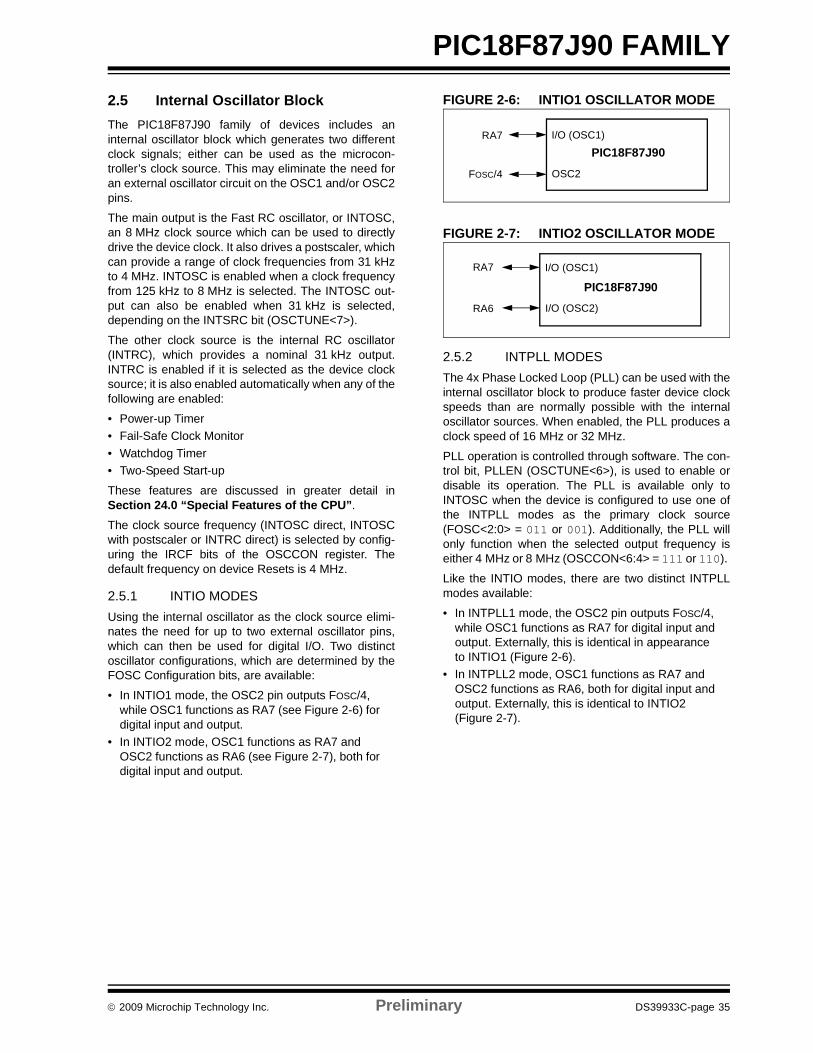
© 2009 Microchip Technology Inc. Preliminary DS39933C-page 35
PIC18F87J90 FAMILY2.5 Internal Oscillator BlockThe PIC18F87J90 family of devices includes aninternal oscillator block which generates two differentclock signals; either can be used as the microcon-troller’s clock source. This may eliminate the need foran external oscillator circuit on the OSC1 and/or OSC2pins.
The main output is the Fast RC oscillator, or INTOSC,an 8 MHz clock source which can be used to directlydrive the device clock. It also drives a postscaler, whichcan provide a range of clock frequencies from 31 kHzto 4 MHz. INTOSC is enabled when a clock frequencyfrom 125 kHz to 8 MHz is selected. The INTOSC out-put can also be enabled when 31 kHz is selected,depending on the INTSRC bit (OSCTUNE<7>).
The other clock source is the internal RC oscillator(INTRC), which provides a nominal 31 kHz output.INTRC is enabled if it is selected as the device clocksource; it is also enabled automatically when any of thefollowing are enabled:
• Power-up Timer• Fail-Safe Clock Monitor• Watchdog Timer• Two-Speed Start-up
These features are discussed in greater detail inSection 24.0 “Special Features of the CPU”.
The clock source frequency (INTOSC direct, INTOSCwith postscaler or INTRC direct) is selected by config-uring the IRCF bits of the OSCCON register. Thedefault frequency on device Resets is 4 MHz.
2.5.1 INTIO MODESUsing the internal oscillator as the clock source elimi-nates the need for up to two external oscillator pins,which can then be used for digital I/O. Two distinctoscillator configurations, which are determined by theFOSC Configuration bits, are available:
• In INTIO1 mode, the OSC2 pin outputs FOSC/4, while OSC1 functions as RA7 (see Figure 2-6) for digital input and output.
• In INTIO2 mode, OSC1 functions as RA7 and OSC2 functions as RA6 (see Figure 2-7), both for digital input and output.
FIGURE 2-6: INTIO1 OSCILLATOR MODE
FIGURE 2-7: INTIO2 OSCILLATOR MODE
2.5.2 INTPLL MODESThe 4x Phase Locked Loop (PLL) can be used with theinternal oscillator block to produce faster device clockspeeds than are normally possible with the internaloscillator sources. When enabled, the PLL produces aclock speed of 16 MHz or 32 MHz.
PLL operation is controlled through software. The con-trol bit, PLLEN (OSCTUNE<6>), is used to enable ordisable its operation. The PLL is available only toINTOSC when the device is configured to use one ofthe INTPLL modes as the primary clock source(FOSC<2:0> = 011 or 001). Additionally, the PLL willonly function when the selected output frequency iseither 4 MHz or 8 MHz (OSCCON<6:4> = 111 or 110).
Like the INTIO modes, there are two distinct INTPLLmodes available:
• In INTPLL1 mode, the OSC2 pin outputs FOSC/4, while OSC1 functions as RA7 for digital input and output. Externally, this is identical in appearance to INTIO1 (Figure 2-6).
• In INTPLL2 mode, OSC1 functions as RA7 and OSC2 functions as RA6, both for digital input and output. Externally, this is identical to INTIO2 (Figure 2-7).
OSC2FOSC/4
I/O (OSC1)RA7
PIC18F87J90
I/O (OSC2)RA6
I/O (OSC1)RA7
PIC18F87J90
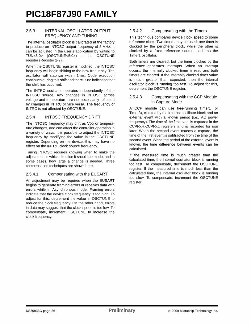
PIC18F87J90 FAMILY
DS39933C-page 36 Preliminary © 2009 Microchip Technology Inc.
2.5.3 INTERNAL OSCILLATOR OUTPUT FREQUENCY AND TUNING
The internal oscillator block is calibrated at the factoryto produce an INTOSC output frequency of 8 MHz. Itcan be adjusted in the user’s application by writing toTUN<5:0> (OSCTUNE<5:0>) in the OSCTUNEregister (Register 2-2).
When the OSCTUNE register is modified, the INTOSCfrequency will begin shifting to the new frequency. Theoscillator will stabilize within 1 ms. Code executioncontinues during this shift and there is no indication thatthe shift has occurred.
The INTRC oscillator operates independently of theINTOSC source. Any changes in INTOSC acrossvoltage and temperature are not necessarily reflectedby changes in INTRC or vice versa. The frequency ofINTRC is not affected by OSCTUNE.
2.5.4 INTOSC FREQUENCY DRIFTThe INTOSC frequency may drift as VDD or tempera-ture changes, and can affect the controller operation ina variety of ways. It is possible to adjust the INTOSCfrequency by modifying the value in the OSCTUNEregister. Depending on the device, this may have noeffect on the INTRC clock source frequency.
Tuning INTOSC requires knowing when to make theadjustment, in which direction it should be made, and insome cases, how large a change is needed. Threecompensation techniques are shown here.
2.5.4.1 Compensating with the EUSART An adjustment may be required when the EUSARTbegins to generate framing errors or receives data witherrors while in Asynchronous mode. Framing errorsindicate that the device clock frequency is too high. Toadjust for this, decrement the value in OSCTUNE toreduce the clock frequency. On the other hand, errorsin data may suggest that the clock speed is too low. Tocompensate, increment OSCTUNE to increase theclock frequency.
2.5.4.2 Compensating with the TimersThis technique compares device clock speed to somereference clock. Two timers may be used; one timer isclocked by the peripheral clock, while the other isclocked by a fixed reference source, such as theTimer1 oscillator.
Both timers are cleared, but the timer clocked by thereference generates interrupts. When an interruptoccurs, the internally clocked timer is read and bothtimers are cleared. If the internally clocked timer valueis much greater than expected, then the internaloscillator block is running too fast. To adjust for this,decrement the OSCTUNE register.
2.5.4.3 Compensating with the CCP Module in Capture Mode
A CCP module can use free-running Timer1 (orTimer3), clocked by the internal oscillator block and anexternal event with a known period (i.e., AC powerfrequency). The time of the first event is captured in theCCPRxH:CCPRxL registers and is recorded for uselater. When the second event causes a capture, thetime of the first event is subtracted from the time of thesecond event. Since the period of the external event isknown, the time difference between events can becalculated.
If the measured time is much greater than thecalculated time, the internal oscillator block is runningtoo fast. To compensate, decrement the OSCTUNEregister. If the measured time is much less than thecalculated time, the internal oscillator block is runningtoo slow. To compensate, increment the OSCTUNEregister.
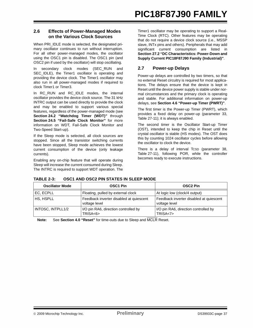
© 2009 Microchip Technology Inc. Preliminary DS39933C-page 37
PIC18F87J90 FAMILY2.6 Effects of Power-Managed Modes
on the Various Clock SourcesWhen PRI_IDLE mode is selected, the designated pri-mary oscillator continues to run without interruption.For all other power-managed modes, the oscillatorusing the OSC1 pin is disabled. The OSC1 pin (andOSC2 pin if used by the oscillator) will stop oscillating.
In secondary clock modes (SEC_RUN andSEC_IDLE), the Timer1 oscillator is operating andproviding the device clock. The Timer1 oscillator mayalso run in all power-managed modes if required toclock Timer1 or Timer3.
In RC_RUN and RC_IDLE modes, the internaloscillator provides the device clock source. The 31 kHzINTRC output can be used directly to provide the clockand may be enabled to support various specialfeatures, regardless of the power-managed mode (seeSection 24.2 “Watchdog Timer (WDT)” throughSection 24.5 “Fail-Safe Clock Monitor” for moreinformation on WDT, Fail-Safe Clock Monitor andTwo-Speed Start-up).
If the Sleep mode is selected, all clock sources arestopped. Since all the transistor switching currentshave been stopped, Sleep mode achieves the lowestcurrent consumption of the device (only leakagecurrents).
Enabling any on-chip feature that will operate duringSleep will increase the current consumed during Sleep.The INTRC is required to support WDT operation. The
Timer1 oscillator may be operating to support a Real-Time Clock (RTC). Other features may be operatingthat do not require a device clock source (i.e., MSSPslave, INTx pins and others). Peripherals that may addsignificant current consumption are listed inSection 27.2 “DC Characteristics: Power-Down andSupply Current PIC18F87J90 Family (Industrial)”.
2.7 Power-up DelaysPower-up delays are controlled by two timers, so thatno external Reset circuitry is required for most applica-tions. The delays ensure that the device is kept inReset until the device power supply is stable under nor-mal circumstances and the primary clock is operatingand stable. For additional information on power-updelays, see Section 4.6 “Power-up Timer (PWRT)”.
The first timer is the Power-up Timer (PWRT), whichprovides a fixed delay on power-up (parameter 33,Table 27-11); it is always enabled.
The second timer is the Oscillator Start-up Timer(OST), intended to keep the chip in Reset until thecrystal oscillator is stable (HS modes). The OST doesthis by counting 1024 oscillator cycles before allowingthe oscillator to clock the device.
There is a delay of interval TCSD (parameter 38,Table 27-11), following POR, while the controllerbecomes ready to execute instructions.
TABLE 2-3: OSC1 AND OSC2 PIN STATES IN SLEEP MODE Oscillator Mode OSC1 Pin OSC2 Pin
EC, ECPLL Floating, pulled by external clock At logic low (clock/4 output)HS, HSPLL Feedback inverter disabled at quiescent
voltage levelFeedback inverter disabled at quiescent voltage level
INTOSC, INTPLL1/2 I/O pin RA6, direction controlled by TRISA<6>
I/O pin RA6, direction controlled by TRISA<7>
Note: See Section 4.0 “Reset” for time-outs due to Sleep and MCLR Reset.

PIC18F87J90 FAMILY
DS39933C-page 38 Preliminary © 2009 Microchip Technology Inc.
NOTES:
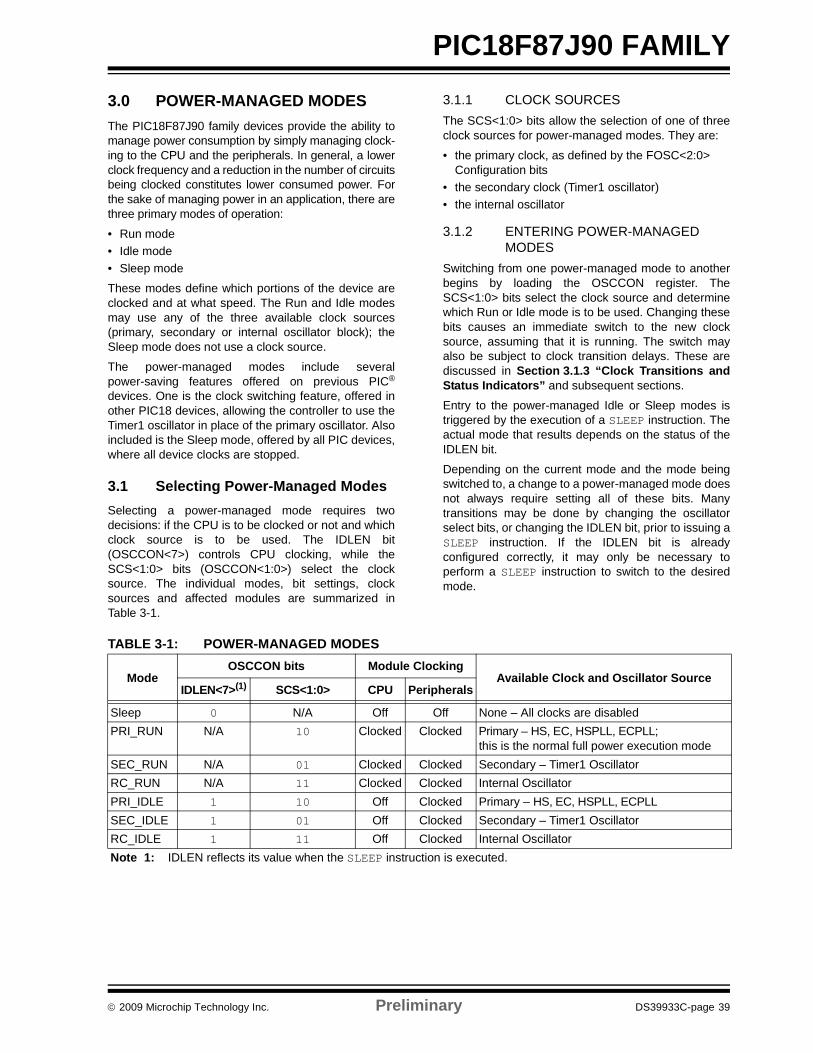
© 2009 Microchip Technology Inc. Preliminary DS39933C-page 39
PIC18F87J90 FAMILY
3.0 POWER-MANAGED MODESThe PIC18F87J90 family devices provide the ability tomanage power consumption by simply managing clock-ing to the CPU and the peripherals. In general, a lowerclock frequency and a reduction in the number of circuitsbeing clocked constitutes lower consumed power. Forthe sake of managing power in an application, there arethree primary modes of operation:
• Run mode• Idle mode • Sleep mode
These modes define which portions of the device areclocked and at what speed. The Run and Idle modesmay use any of the three available clock sources(primary, secondary or internal oscillator block); theSleep mode does not use a clock source.
The power-managed modes include severalpower-saving features offered on previous PIC®
devices. One is the clock switching feature, offered inother PIC18 devices, allowing the controller to use theTimer1 oscillator in place of the primary oscillator. Alsoincluded is the Sleep mode, offered by all PIC devices,where all device clocks are stopped.
3.1 Selecting Power-Managed ModesSelecting a power-managed mode requires twodecisions: if the CPU is to be clocked or not and whichclock source is to be used. The IDLEN bit(OSCCON<7>) controls CPU clocking, while theSCS<1:0> bits (OSCCON<1:0>) select the clocksource. The individual modes, bit settings, clocksources and affected modules are summarized inTable 3-1.
3.1.1 CLOCK SOURCESThe SCS<1:0> bits allow the selection of one of threeclock sources for power-managed modes. They are:
• the primary clock, as defined by the FOSC<2:0> Configuration bits
• the secondary clock (Timer1 oscillator)• the internal oscillator
3.1.2 ENTERING POWER-MANAGED MODES
Switching from one power-managed mode to anotherbegins by loading the OSCCON register. TheSCS<1:0> bits select the clock source and determinewhich Run or Idle mode is to be used. Changing thesebits causes an immediate switch to the new clocksource, assuming that it is running. The switch mayalso be subject to clock transition delays. These arediscussed in Section 3.1.3 “Clock Transitions andStatus Indicators” and subsequent sections.
Entry to the power-managed Idle or Sleep modes istriggered by the execution of a SLEEP instruction. Theactual mode that results depends on the status of theIDLEN bit.
Depending on the current mode and the mode beingswitched to, a change to a power-managed mode doesnot always require setting all of these bits. Manytransitions may be done by changing the oscillatorselect bits, or changing the IDLEN bit, prior to issuing aSLEEP instruction. If the IDLEN bit is alreadyconfigured correctly, it may only be necessary toperform a SLEEP instruction to switch to the desiredmode.
TABLE 3-1: POWER-MANAGED MODES
ModeOSCCON bits Module Clocking
Available Clock and Oscillator SourceIDLEN<7>(1) SCS<1:0> CPU Peripherals
Sleep 0 N/A Off Off None – All clocks are disabledPRI_RUN N/A 10 Clocked Clocked Primary – HS, EC, HSPLL, ECPLL;
this is the normal full power execution modeSEC_RUN N/A 01 Clocked Clocked Secondary – Timer1 OscillatorRC_RUN N/A 11 Clocked Clocked Internal OscillatorPRI_IDLE 1 10 Off Clocked Primary – HS, EC, HSPLL, ECPLLSEC_IDLE 1 01 Off Clocked Secondary – Timer1 OscillatorRC_IDLE 1 11 Off Clocked Internal OscillatorNote 1: IDLEN reflects its value when the SLEEP instruction is executed.
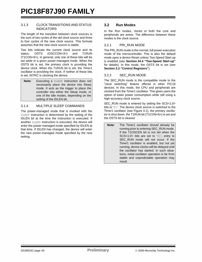
PIC18F87J90 FAMILY
DS39933C-page 40 Preliminary © 2009 Microchip Technology Inc.
3.1.3 CLOCK TRANSITIONS AND STATUS INDICATORS
The length of the transition between clock sources isthe sum of two cycles of the old clock source and threeto four cycles of the new clock source. This formulaassumes that the new clock source is stable.
Two bits indicate the current clock source and itsstatus: OSTS (OSCCON<3>) and T1RUN(T1CON<6>). In general, only one of these bits will beset while in a given power-managed mode. When theOSTS bit is set, the primary clock is providing thedevice clock. When the T1RUN bit is set, the Timer1oscillator is providing the clock. If neither of these bitsis set, INTRC is clocking the device.
3.1.4 MULTIPLE SLEEP COMMANDSThe power-managed mode that is invoked with theSLEEP instruction is determined by the setting of theIDLEN bit at the time the instruction is executed. Ifanother SLEEP instruction is executed, the device willenter the power-managed mode specified by IDLEN atthat time. If IDLEN has changed, the device will enterthe new power-managed mode specified by the newsetting.
3.2 Run ModesIn the Run modes, clocks to both the core andperipherals are active. The difference between thesemodes is the clock source.
3.2.1 PRI_RUN MODEThe PRI_RUN mode is the normal, full power executionmode of the microcontroller. This is also the defaultmode upon a device Reset unless Two-Speed Start-upis enabled (see Section 24.4 “Two-Speed Start-up”for details). In this mode, the OSTS bit is set (seeSection 2.2 “Control Registers”).
3.2.2 SEC_RUN MODEThe SEC_RUN mode is the compatible mode to the“clock switching” feature offered in other PIC18devices. In this mode, the CPU and peripherals areclocked from the Timer1 oscillator. This gives users theoption of lower power consumption while still using ahigh-accuracy clock source.
SEC_RUN mode is entered by setting the SCS<1:0>bits to ‘01’. The device clock source is switched to theTimer1 oscillator (see Figure 3-1), the primary oscilla-tor is shut down, the T1RUN bit (T1CON<6>) is set andthe OSTS bit is cleared.
Note: Executing a SLEEP instruction does notnecessarily place the device into Sleepmode. It acts as the trigger to place thecontroller into either the Sleep mode, orone of the Idle modes, depending on thesetting of the IDLEN bit.
Note: The Timer1 oscillator should already berunning prior to entering SEC_RUN mode.If the T1OSCEN bit is not set when theSCS<1:0> bits are set to ‘01’, entry toSEC_RUN mode will not occur. If theTimer1 oscillator is enabled, but not yetrunning, device clocks will be delayed untilthe oscillator has started. In such situa-tions, initial oscillator operation is far fromstable and unpredictable operation mayresult.
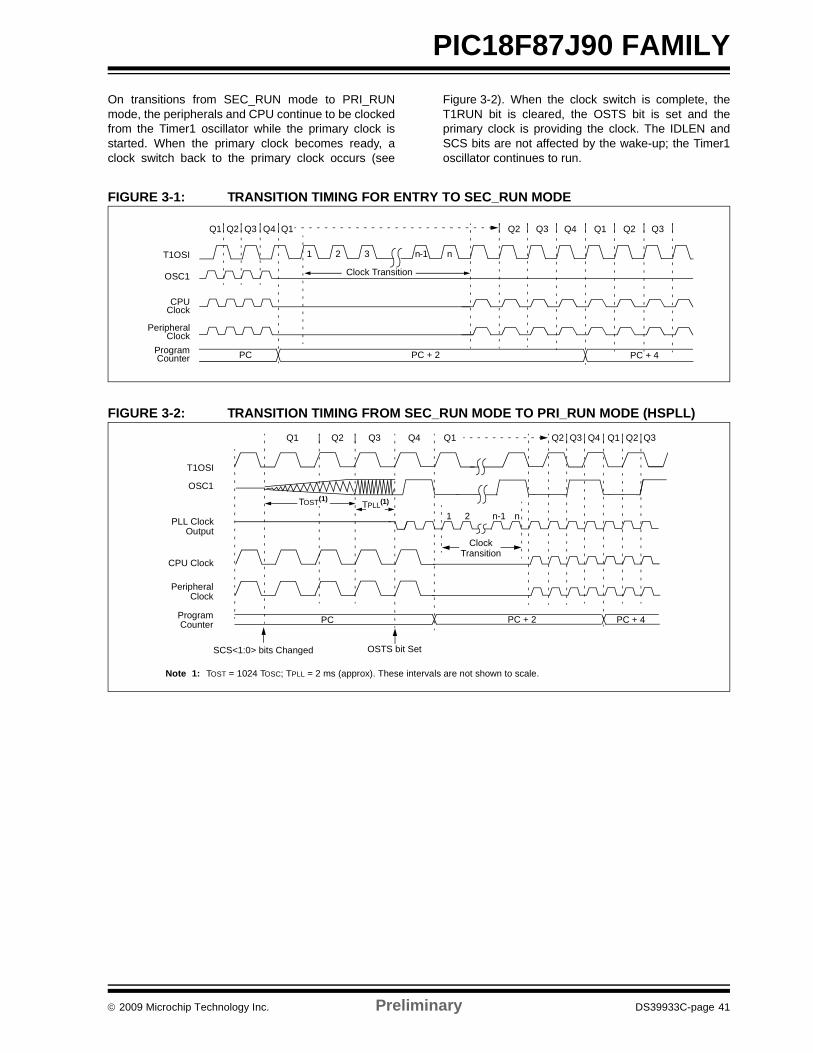
© 2009 Microchip Technology Inc. Preliminary DS39933C-page 41
PIC18F87J90 FAMILYOn transitions from SEC_RUN mode to PRI_RUNmode, the peripherals and CPU continue to be clockedfrom the Timer1 oscillator while the primary clock isstarted. When the primary clock becomes ready, aclock switch back to the primary clock occurs (see
Figure 3-2). When the clock switch is complete, theT1RUN bit is cleared, the OSTS bit is set and theprimary clock is providing the clock. The IDLEN andSCS bits are not affected by the wake-up; the Timer1oscillator continues to run.
FIGURE 3-1: TRANSITION TIMING FOR ENTRY TO SEC_RUN MODE
FIGURE 3-2: TRANSITION TIMING FROM SEC_RUN MODE TO PRI_RUN MODE (HSPLL)
Q4Q3Q2
OSC1
Peripheral
Program
Q1
T1OSI
Q1
Counter
Clock
CPUClock
PC + 2PC
1 2 3 n-1 n
Clock Transition
Q4Q3Q2 Q1 Q3Q2
PC + 4
Q1 Q3 Q4
OSC1
Peripheral
Program PC
T1OSI
PLL Clock
Q1
PC + 4
Q2
Output
Q3 Q4 Q1
CPU Clock
PC + 2
Clock
Counter
Q2 Q2 Q3
Note 1: TOST = 1024 TOSC; TPLL = 2 ms (approx). These intervals are not shown to scale.
SCS<1:0> bits Changed
TPLL(1)
1 2 n-1 n
Clock
OSTS bit Set
Transition
TOST(1)
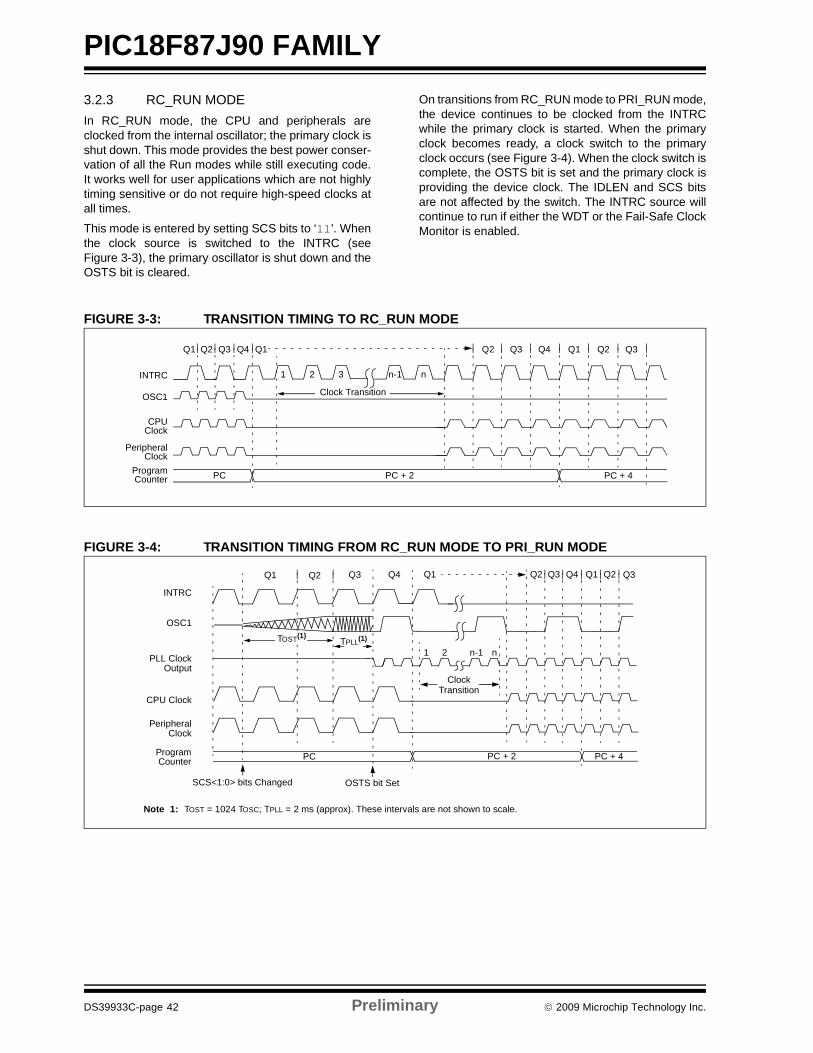
PIC18F87J90 FAMILY
DS39933C-page 42 Preliminary © 2009 Microchip Technology Inc.
3.2.3 RC_RUN MODEIn RC_RUN mode, the CPU and peripherals areclocked from the internal oscillator; the primary clock isshut down. This mode provides the best power conser-vation of all the Run modes while still executing code.It works well for user applications which are not highlytiming sensitive or do not require high-speed clocks atall times.
This mode is entered by setting SCS bits to ‘11’. Whenthe clock source is switched to the INTRC (seeFigure 3-3), the primary oscillator is shut down and theOSTS bit is cleared.
On transitions from RC_RUN mode to PRI_RUN mode,the device continues to be clocked from the INTRCwhile the primary clock is started. When the primaryclock becomes ready, a clock switch to the primaryclock occurs (see Figure 3-4). When the clock switch iscomplete, the OSTS bit is set and the primary clock isproviding the device clock. The IDLEN and SCS bitsare not affected by the switch. The INTRC source willcontinue to run if either the WDT or the Fail-Safe ClockMonitor is enabled.
FIGURE 3-3: TRANSITION TIMING TO RC_RUN MODE
FIGURE 3-4: TRANSITION TIMING FROM RC_RUN MODE TO PRI_RUN MODE
Q4Q3Q2
OSC1
Peripheral
Program
Q1
INTRC
Q1
Counter
Clock
CPUClock
PC + 2PC
1 2 3 n-1 n
Clock Transition
Q4Q3Q2 Q1 Q3Q2
PC + 4
Q1 Q3 Q4
OSC1
Peripheral
Program PC
INTRC
PLL Clock
Q1
PC + 4
Q2
Output
Q3 Q4 Q1
CPU Clock
PC + 2
Clock
Counter
Q2 Q2 Q3
Note 1: TOST = 1024 TOSC; TPLL = 2 ms (approx). These intervals are not shown to scale.
SCS<1:0> bits Changed
TPLL(1)
1 2 n-1 n
Clock
OSTS bit Set
Transition
TOST(1)
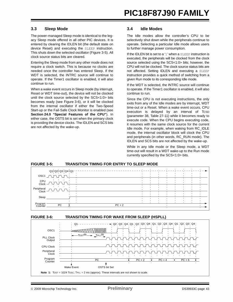
© 2009 Microchip Technology Inc. Preliminary DS39933C-page 43
PIC18F87J90 FAMILY3.3 Sleep ModeThe power-managed Sleep mode is identical to the leg-acy Sleep mode offered in all other PIC devices. It isentered by clearing the IDLEN bit (the default state ondevice Reset) and executing the SLEEP instruction.This shuts down the selected oscillator (Figure 3-5). Allclock source status bits are cleared.
Entering the Sleep mode from any other mode does notrequire a clock switch. This is because no clocks areneeded once the controller has entered Sleep. If theWDT is selected, the INTRC source will continue tooperate. If the Timer1 oscillator is enabled, it will alsocontinue to run.
When a wake event occurs in Sleep mode (by interrupt,Reset or WDT time-out), the device will not be clockeduntil the clock source selected by the SCS<1:0> bitsbecomes ready (see Figure 3-6), or it will be clockedfrom the internal oscillator if either the Two-SpeedStart-up or the Fail-Safe Clock Monitor is enabled (seeSection 24.0 “Special Features of the CPU”). Ineither case, the OSTS bit is set when the primary clockis providing the device clocks. The IDLEN and SCS bitsare not affected by the wake-up.
3.4 Idle ModesThe Idle modes allow the controller’s CPU to beselectively shut down while the peripherals continue tooperate. Selecting a particular Idle mode allows usersto further manage power consumption.
If the IDLEN bit is set to a ‘1’ when a SLEEP instruction isexecuted, the peripherals will be clocked from the clocksource selected using the SCS<1:0> bits; however, theCPU will not be clocked. The clock source status bits arenot affected. Setting IDLEN and executing a SLEEPinstruction provides a quick method of switching from agiven Run mode to its corresponding Idle mode.
If the WDT is selected, the INTRC source will continueto operate. If the Timer1 oscillator is enabled, it will alsocontinue to run.
Since the CPU is not executing instructions, the onlyexits from any of the Idle modes are by interrupt, WDTtime-out or a Reset. When a wake event occurs, CPUexecution is delayed by an interval of TCSD(parameter 38, Table 27-11) while it becomes ready toexecute code. When the CPU begins executing code,it resumes with the same clock source for the currentIdle mode. For example, when waking from RC_IDLEmode, the internal oscillator block will clock the CPUand peripherals (in other words, RC_RUN mode). TheIDLEN and SCS bits are not affected by the wake-up.
While in any Idle mode or the Sleep mode, a WDTtime-out will result in a WDT wake-up to the Run modecurrently specified by the SCS<1:0> bits.
FIGURE 3-5: TRANSITION TIMING FOR ENTRY TO SLEEP MODE
FIGURE 3-6: TRANSITION TIMING FOR WAKE FROM SLEEP (HSPLL)
Q4Q3Q2
OSC1
Peripheral
Sleep
Program
Q1Q1
Counter
Clock
CPUClock
PC + 2PC
Q3 Q4 Q1 Q2
OSC1
Peripheral
Program PC
PLL Clock
Q3 Q4
Output
CPU Clock
Q1 Q2 Q3 Q4 Q1 Q2
Clock
Counter PC + 6PC + 4
Q1 Q2 Q3 Q4
Wake Event
Note 1: TOST = 1024 TOSC; TPLL = 2 ms (approx). These intervals are not shown to scale.
TOST(1) TPLL(1)
OSTS bit Set
PC + 2
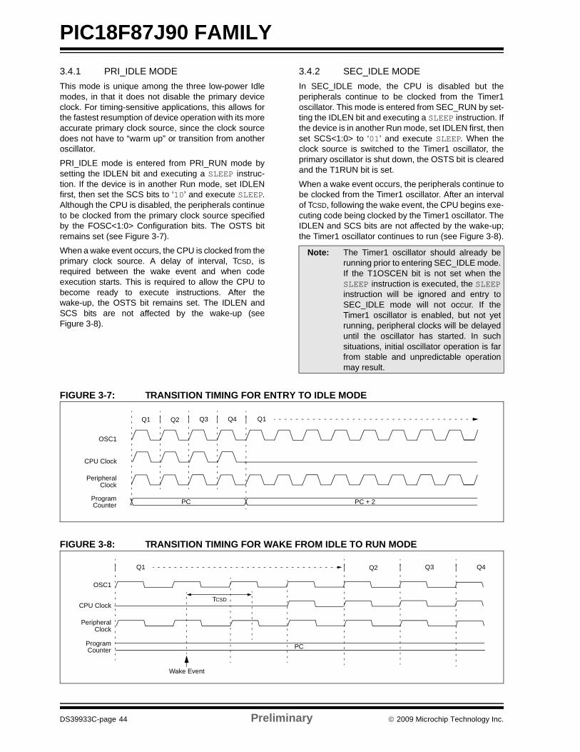
PIC18F87J90 FAMILY
DS39933C-page 44 Preliminary © 2009 Microchip Technology Inc.
3.4.1 PRI_IDLE MODEThis mode is unique among the three low-power Idlemodes, in that it does not disable the primary deviceclock. For timing-sensitive applications, this allows forthe fastest resumption of device operation with its moreaccurate primary clock source, since the clock sourcedoes not have to “warm up” or transition from anotheroscillator.
PRI_IDLE mode is entered from PRI_RUN mode bysetting the IDLEN bit and executing a SLEEP instruc-tion. If the device is in another Run mode, set IDLENfirst, then set the SCS bits to ‘10’ and execute SLEEP.Although the CPU is disabled, the peripherals continueto be clocked from the primary clock source specifiedby the FOSC<1:0> Configuration bits. The OSTS bitremains set (see Figure 3-7).
When a wake event occurs, the CPU is clocked from theprimary clock source. A delay of interval, TCSD, isrequired between the wake event and when codeexecution starts. This is required to allow the CPU tobecome ready to execute instructions. After thewake-up, the OSTS bit remains set. The IDLEN andSCS bits are not affected by the wake-up (seeFigure 3-8).
3.4.2 SEC_IDLE MODEIn SEC_IDLE mode, the CPU is disabled but theperipherals continue to be clocked from the Timer1oscillator. This mode is entered from SEC_RUN by set-ting the IDLEN bit and executing a SLEEP instruction. Ifthe device is in another Run mode, set IDLEN first, thenset SCS<1:0> to ‘01’ and execute SLEEP. When theclock source is switched to the Timer1 oscillator, theprimary oscillator is shut down, the OSTS bit is clearedand the T1RUN bit is set.
When a wake event occurs, the peripherals continue tobe clocked from the Timer1 oscillator. After an intervalof TCSD, following the wake event, the CPU begins exe-cuting code being clocked by the Timer1 oscillator. TheIDLEN and SCS bits are not affected by the wake-up;the Timer1 oscillator continues to run (see Figure 3-8).
FIGURE 3-7: TRANSITION TIMING FOR ENTRY TO IDLE MODE
FIGURE 3-8: TRANSITION TIMING FOR WAKE FROM IDLE TO RUN MODE
Note: The Timer1 oscillator should already berunning prior to entering SEC_IDLE mode.If the T1OSCEN bit is not set when theSLEEP instruction is executed, the SLEEPinstruction will be ignored and entry toSEC_IDLE mode will not occur. If theTimer1 oscillator is enabled, but not yetrunning, peripheral clocks will be delayeduntil the oscillator has started. In suchsituations, initial oscillator operation is farfrom stable and unpredictable operationmay result.
Q1
Peripheral
Program PC PC + 2
OSC1
Q3 Q4 Q1
CPU Clock
Clock
Counter
Q2
OSC1
Peripheral
Program PC
CPU Clock
Q1 Q3 Q4
Clock
Counter
Q2
Wake Event
TCSD
© 2009 Microchip Technology Inc. Preliminary DS39933C-page 45
PIC18F87J90 FAMILY3.4.3 RC_IDLE MODEIn RC_IDLE mode, the CPU is disabled but the periph-erals continue to be clocked from the internal oscillator.This mode allows for controllable power conservationduring Idle periods.
From RC_RUN, this mode is entered by setting theIDLEN bit and executing a SLEEP instruction. If thedevice is in another Run mode, first set IDLEN, thenclear the SCS bits and execute SLEEP. When the clocksource is switched to the INTRC, the primary oscillatoris shut down and the OSTS bit is cleared.
When a wake event occurs, the peripherals continue tobe clocked from the INTOSC. After a delay of TCSD,following the wake event, the CPU begins executingcode being clocked by the INTOSC. The IDLEN andSCS bits are not affected by the wake-up. The INTOSCsource will continue to run if either the WDT or theFail-Safe Clock Monitor is enabled.
3.5 Exiting Idle and Sleep ModesAn exit from Sleep mode, or any of the Idle modes, istriggered by an interrupt, a Reset or a WDT time-out.This section discusses the triggers that cause exitsfrom power-managed modes. The clocking subsystemactions are discussed in each of the power-managedmode sections (see Section 3.2 “Run Modes”,Section 3.3 “Sleep Mode” and Section 3.4 “IdleModes”).
3.5.1 EXIT BY INTERRUPTAny of the available interrupt sources can cause thedevice to exit from an Idle mode, or the Sleep mode, toa Run mode. To enable this functionality, an interruptsource must be enabled by setting its enable bit in oneof the INTCON or PIE registers. The exit sequence isinitiated when the corresponding interrupt flag bit is set.
On all exits from Idle or Sleep modes by interrupt, codeexecution branches to the interrupt vector if theGIE/GIEH bit (INTCON<7>) is set. Otherwise, codeexecution continues or resumes without branching(see Section 8.0 “Interrupts”).
A fixed delay of interval TCSD following the wake eventis required when leaving Sleep and Idle modes. Thisdelay is required for the CPU to prepare for execution.Instruction execution resumes on the first clock cyclefollowing this delay.
3.5.2 EXIT BY WDT TIME-OUTA WDT time-out will cause different actions dependingon which power-managed mode the device is in whenthe time-out occurs.
If the device is not executing code (all Idle modes andSleep mode), the time-out will result in an exit from thepower-managed mode (see Section 3.2 “RunModes” and Section 3.3 “Sleep Mode”). If the deviceis executing code (all Run modes), the time-out willresult in a WDT Reset (see Section 24.2 “WatchdogTimer (WDT)”).
The Watchdog Timer and postscaler are cleared by oneof the following events:
• executing a SLEEP or CLRWDT instruction • the loss of a currently selected clock source (if the
Fail-Safe Clock Monitor is enabled)
3.5.3 EXIT BY RESETExiting an Idle or Sleep mode by Reset automaticallyforces the device to run from the INTRC.
3.5.4 EXIT WITHOUT AN OSCILLATOR START-UP DELAY
Certain exits from power-managed modes do notinvoke the OST at all. There are two cases:
• PRI_IDLE mode, where the primary clock source is not stopped; and
• the primary clock source is either the EC or ECPLL mode.
In these instances, the primary clock source eitherdoes not require an oscillator start-up delay, since it isalready running (PRI_IDLE), or normally does notrequire an oscillator start-up delay (EC). However, afixed delay of interval TCSD following the wake event isstill required when leaving Sleep and Idle modes toallow the CPU to prepare for execution. Instructionexecution resumes on the first clock cycle following thisdelay.

PIC18F87J90 FAMILY
DS39933C-page 46 Preliminary © 2009 Microchip Technology Inc.
NOTES:
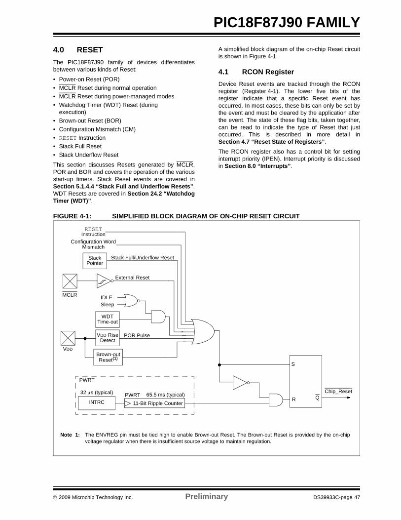
© 2009 Microchip Technology Inc. Preliminary DS39933C-page 47
PIC18F87J90 FAMILY
4.0 RESETThe PIC18F87J90 family of devices differentiatesbetween various kinds of Reset:
• Power-on Reset (POR) • MCLR Reset during normal operation• MCLR Reset during power-managed modes • Watchdog Timer (WDT) Reset (during
execution)• Brown-out Reset (BOR) • Configuration Mismatch (CM)• RESET Instruction• Stack Full Reset• Stack Underflow Reset
This section discusses Resets generated by MCLR,POR and BOR and covers the operation of the variousstart-up timers. Stack Reset events are covered inSection 5.1.4.4 “Stack Full and Underflow Resets”.WDT Resets are covered in Section 24.2 “WatchdogTimer (WDT)”.
A simplified block diagram of the on-chip Reset circuitis shown in Figure 4-1.
4.1 RCON RegisterDevice Reset events are tracked through the RCONregister (Register 4-1). The lower five bits of theregister indicate that a specific Reset event hasoccurred. In most cases, these bits can only be set bythe event and must be cleared by the application afterthe event. The state of these flag bits, taken together,can be read to indicate the type of Reset that justoccurred. This is described in more detail inSection 4.7 “Reset State of Registers”.
The RCON register also has a control bit for settinginterrupt priority (IPEN). Interrupt priority is discussedin Section 8.0 “Interrupts”.
FIGURE 4-1: SIMPLIFIED BLOCK DIAGRAM OF ON-CHIP RESET CIRCUIT
S
R Q
External Reset
MCLR
VDD
WDTTime-out
VDD RiseDetect
PWRT
INTRC
POR Pulse
PWRTChip_Reset
11-Bit Ripple Counter
Brown-outReset(1)
RESETInstruction
StackPointer
Stack Full/Underflow Reset
SleepIDLE
65.5 ms (typical)
Note 1: The ENVREG pin must be tied high to enable Brown-out Reset. The Brown-out Reset is provided by the on-chipvoltage regulator when there is insufficient source voltage to maintain regulation.
Configuration WordMismatch
32 μs (typical)
PIC18F87J90 FAMILY
DS39933C-page 48 Preliminary © 2009 Microchip Technology Inc.
REGISTER 4-1: RCON: RESET CONTROL REGISTER
R/W-0 U-0 R/W-1 R/W-1 R-1 R-1 R/W-0 R/W-0
IPEN — CM RI TO PD POR BORbit 7 bit 0
Legend:R = Readable bit W = Writable bit U = Unimplemented bit, read as ‘0’-n = Value at POR ‘1’ = Bit is set ‘0’ = Bit is cleared x = Bit is unknown
bit 7 IPEN: Interrupt Priority Enable bit 1 = Enable priority levels on interrupts0 = Disable priority levels on interrupts (PIC16XXXX Compatibility mode)
bit 6 Unimplemented: Read as ‘0’ bit 5 CM: Configuration Mismatch Flag bit
1 = A configuration mismatch has not occurred0 = A configuration mismatch has occurred (Must be set in software after a Configuration Mismatch
Reset occurs.)bit 4 RI: RESET Instruction Flag bit
1 = The RESET instruction was not executed (set by firmware only)0 = The RESET instruction was executed causing a device Reset (must be set in software after a
Brown-out Reset occurs)bit 3 TO: Watchdog Time-out Flag bit
1 = Set by power-up, CLRWDT instruction or SLEEP instruction 0 = A WDT time-out occurred
bit 2 PD: Power-Down Detection Flag bit 1 = Set by power-up or by the CLRWDT instruction 0 = Set by execution of the SLEEP instruction
bit 1 POR: Power-on Reset Status bit 1 = A Power-on Reset has not occurred (set by firmware only)0 = A Power-on Reset occurred (must be set in software after a Power-on Reset occurs)
bit 0 BOR: Brown-out Reset Status bit1 = A Brown-out Reset has not occurred (set by firmware only)0 = A Brown-out Reset occurred (must be set in software after a Brown-out Reset occurs)
Note 1: It is recommended that the POR bit be set after a Power-on Reset has been detected, so that subsequentPower-on Resets may be detected.
2: If the on-chip voltage regulator is disabled, BOR remains ‘0’ at all times. See Section 4.4.1 “DetectingBOR” for more information.
3: Brown-out Reset is said to have occurred when BOR is ‘0’ and POR is ‘1’ (assuming that POR was set to‘1’ by software immediately after a Power-on Reset).
© 2009 Microchip Technology Inc. Preliminary DS39933C-page 49
PIC18F87J90 FAMILY4.2 Master Clear (MCLR)The MCLR pin provides a method for triggering a hardexternal Reset of the device. A Reset is generated byholding the pin low. PIC18 extended microcontrollerdevices have a noise filter in the MCLR Reset pathwhich detects and ignores small pulses.
The MCLR pin is not driven low by any internal Resets,including the WDT.
4.3 Power-on Reset (POR)A Power-on Reset condition is generated on-chipwhenever VDD rises above a certain threshold. Thisallows the device to start in the initialized state whenVDD is adequate for operation.
To take advantage of the POR circuitry, tie the MCLRpin through a resistor (1 kΩ to 10 kΩ) to VDD. This willeliminate external RC components usually needed tocreate a Power-on Reset delay. A minimum rise rate forVDD is specified (parameter D004). For a slow risetime, see Figure 4-2.
When the device starts normal operation (i.e., exits theReset condition), device operating parameters(voltage, frequency, temperature, etc.) must be met toensure operation. If these conditions are not met, thedevice must be held in Reset until the operatingconditions are met.
Power-on Reset events are captured by the POR bit(RCON<1>). The state of the bit is set to ‘0’ whenevera Power-on Reset occurs; it does not change for anyother Reset event. POR is not reset to ‘1’ by anyhardware event. To capture multiple events, the usermanually resets the bit to ‘1’ in software following anyPower-on Reset.
4.4 Brown-out Reset (BOR)The PIC18F87J90 family of devices incorporates asimple BOR function when the internal regulator isenabled (ENVREG pin is tied to VDD). The voltage reg-ulator will trigger a Brown-out Reset when output of theregulator to the device core approaches the voltage atwhich the device is unable to run at full speed. TheBOR circuit also keeps the device in Reset as VDDrises, until the regulator’s output level is sufficient forfull-speed operation.
Once a BOR has occurred, the Power-up Timer willkeep the chip in Reset for TPWRT (parameter 33). IfVDD drops below the threshold for full-speed operationwhile the Power-up Timer is running, the chip will goback into a Brown-out Reset and the Power-up Timerwill be initialized. Once VDD rises to the point whereregulator output is sufficient, the Power-up Timer willexecute the additional time delay.
FIGURE 4-2: EXTERNAL POWER-ON RESET CIRCUIT (FOR SLOW VDD POWER-UP)
4.4.1 DETECTING BORThe BOR bit always resets to ‘0’ on any Brown-outReset or Power-on Reset event. This makes it difficultto determine if a Brown-out Reset event has occurredjust by reading the state of BOR alone. A more reliablemethod is to simultaneously check the state of bothPOR and BOR. This assumes that the POR bit is resetto ‘1’ in software immediately after any Power-on Resetevent. If BOR is ‘0’ while POR is ‘1’, it can be reliablyassumed that a Brown-out Reset event has occurred.
If the voltage regulator is disabled, Brown-out Resetfunctionality is disabled. In this case, the BOR bitcannot be used to determine a Brown-out Reset event.The BOR bit is still cleared by a Power-on Reset event.
4.5 Configuration Mismatch (CM)The Configuration Mismatch (CM) Reset is designed todetect and attempt to recover from random, memorycorrupting events. These include ElectrostaticDischarge (ESD) events that can cause widespread,single bit changes throughout the device and result incatastrophic failure.
In PIC18FXXJ Flash devices, the device Configurationregisters (located in the configuration memory space)are continuously monitored during operation by com-paring their values to complimentary shadow registers.If a mismatch is detected between the two sets of reg-isters, a CM Reset automatically occurs. These eventsare captured by the CM bit (RCON<5>). The state ofthe bit is set to ‘0’ whenever a CM event occurs. The bitdoes not change for any other Reset event.
Note 1: External Power-on Reset circuit is requiredonly if the VDD power-up slope is too slow.The diode D helps discharge the capacitorquickly when VDD powers down.
2: R < 40 kΩ is recommended to make sure thatthe voltage drop across R does not violatethe device’s electrical specification.
3: R1 ≥ 1 kΩ will limit any current flowing intoMCLR from external capacitor C, in the eventof MCLR/VPP pin breakdown, due toElectrostatic Discharge (ESD) or ElectricalOverstress (EOS).
C
R1RD
VDD
MCLR
VDD
PIC18F87J90
PIC18F87J90 FAMILY
DS39933C-page 50 Preliminary © 2009 Microchip Technology Inc.
4.6 Power-up Timer (PWRT)PIC18F87J90 family devices incorporate an on-chipPower-up Timer (PWRT) to help regulate the Power-onReset process. The PWRT is always enabled. Themain function is to ensure that the device voltage isstable before code is executed.
The Power-up Timer (PWRT) of the PIC18F87J90 fam-ily devices is an 11-bit counter which uses the INTRCsource as the clock input. This yields an approximatetime interval of 2048 x 32 μs = 65.6 ms. While thePWRT is counting, the device is held in Reset.
The power-up time delay depends on the INTRC clockand will vary from chip to chip due to temperature andprocess variation. See DC parameter 33 for details.
4.6.1 TIME-OUT SEQUENCEIf enabled, the PWRT time-out is invoked after the PORpulse has cleared. The total time-out will vary based onthe status of the PWRT. Figure 4-3, Figure 4-4,Figure 4-5 and Figure 4-6 all depict time-outsequences on power-up with the Power-up Timerenabled.
Since the time-outs occur from the POR pulse, if MCLRis kept low long enough, the PWRT will expire. BringingMCLR high will begin execution immediately(Figure 4-5). This is useful for testing purposes, or tosynchronize more than one PIC18FXXXX deviceoperating in parallel.
FIGURE 4-3: TIME-OUT SEQUENCE ON POWER-UP (MCLR TIED TO VDD, VDD RISE < TPWRT)
FIGURE 4-4: TIME-OUT SEQUENCE ON POWER-UP (MCLR NOT TIED TO VDD): CASE 1
TPWRT
VDD
MCLR
INTERNAL POR
PWRT TIME-OUT
INTERNAL RESET
TPWRT
VDD
MCLR
INTERNAL POR
PWRT TIME-OUT
INTERNAL RESET
© 2009 Microchip Technology Inc. Preliminary DS39933C-page 51
PIC18F87J90 FAMILYFIGURE 4-5: TIME-OUT SEQUENCE ON POWER-UP (MCLR NOT TIED TO VDD): CASE 2
FIGURE 4-6: SLOW RISE TIME (MCLR TIED TO VDD, VDD RISE > TPWRT)
VDD
MCLR
INTERNAL POR
PWRT TIME-OUT
INTERNAL RESET
TPWRT
VDD
MCLR
INTERNAL POR
PWRT TIME-OUT
INTERNAL RESET
0V 1V
3.3V
TPWRT
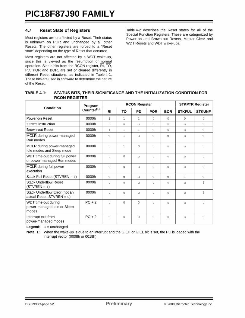
PIC18F87J90 FAMILY
DS39933C-page 52 Preliminary © 2009 Microchip Technology Inc.
4.7 Reset State of RegistersMost registers are unaffected by a Reset. Their statusis unknown on POR and unchanged by all otherResets. The other registers are forced to a “Resetstate” depending on the type of Reset that occurred.
Most registers are not affected by a WDT wake-up,since this is viewed as the resumption of normaloperation. Status bits from the RCON register, RI, TO,PD, POR and BOR, are set or cleared differently indifferent Reset situations, as indicated in Table 4-1.These bits are used in software to determine the natureof the Reset.
Table 4-2 describes the Reset states for all of theSpecial Function Registers. These are categorized byPower-on and Brown-out Resets, Master Clear andWDT Resets and WDT wake-ups.
TABLE 4-1: STATUS BITS, THEIR SIGNIFICANCE AND THE INITIALIZATION CONDITION FOR RCON REGISTER
Condition Program Counter(1)
RCON Register STKPTR Register
RI TO PD POR BOR STKFUL STKUNF
Power-on Reset 0000h 1 1 1 0 0 0 0
RESET Instruction 0000h 0 u u u u u u
Brown-out Reset 0000h 1 1 1 u 0 u u
MCLR during power-managed Run modes
0000h u 1 u u u u u
MCLR during power-managed Idle modes and Sleep mode
0000h u 1 0 u u u u
WDT time-out during full power or power-managed Run modes
0000h u 0 u u u u u
MCLR during full power execution
0000h u u u u u u u
Stack Full Reset (STVREN = 1) 0000h u u u u u 1 u
Stack Underflow Reset (STVREN = 1)
0000h u u u u u u 1
Stack Underflow Error (not an actual Reset, STVREN = 0)
0000h u u u u u u 1
WDT time-out during power-managed Idle or Sleep modes
PC + 2 u 0 0 u u u u
Interrupt exit from power-managed modes
PC + 2 u u 0 u u u u
Legend: u = unchangedNote 1: When the wake-up is due to an interrupt and the GIEH or GIEL bit is set, the PC is loaded with the
interrupt vector (0008h or 0018h).
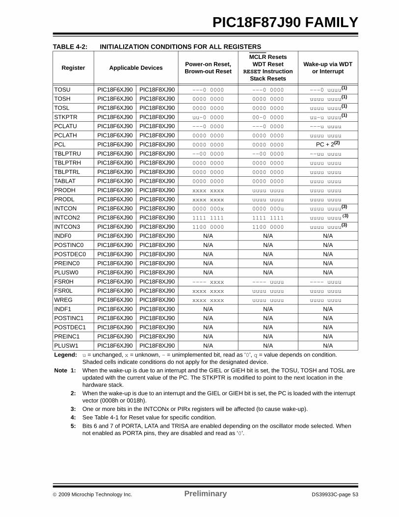
© 2009 Microchip Technology Inc. Preliminary DS39933C-page 53
PIC18F87J90 FAMILYTABLE 4-2: INITIALIZATION CONDITIONS FOR ALL REGISTERS
Register Applicable Devices Power-on Reset,Brown-out Reset
MCLR ResetsWDT Reset
RESET InstructionStack Resets
Wake-up via WDT or Interrupt
TOSU PIC18F6XJ90 PIC18F8XJ90 ---0 0000 ---0 0000 ---0 uuuu(1)
TOSH PIC18F6XJ90 PIC18F8XJ90 0000 0000 0000 0000 uuuu uuuu(1)
TOSL PIC18F6XJ90 PIC18F8XJ90 0000 0000 0000 0000 uuuu uuuu(1)
STKPTR PIC18F6XJ90 PIC18F8XJ90 uu-0 0000 00-0 0000 uu-u uuuu(1)
PCLATU PIC18F6XJ90 PIC18F8XJ90 ---0 0000 ---0 0000 ---u uuuu
PCLATH PIC18F6XJ90 PIC18F8XJ90 0000 0000 0000 0000 uuuu uuuu
PCL PIC18F6XJ90 PIC18F8XJ90 0000 0000 0000 0000 PC + 2(2)
TBLPTRU PIC18F6XJ90 PIC18F8XJ90 --00 0000 --00 0000 --uu uuuu
TBLPTRH PIC18F6XJ90 PIC18F8XJ90 0000 0000 0000 0000 uuuu uuuu
TBLPTRL PIC18F6XJ90 PIC18F8XJ90 0000 0000 0000 0000 uuuu uuuu
TABLAT PIC18F6XJ90 PIC18F8XJ90 0000 0000 0000 0000 uuuu uuuu
PRODH PIC18F6XJ90 PIC18F8XJ90 xxxx xxxx uuuu uuuu uuuu uuuu
PRODL PIC18F6XJ90 PIC18F8XJ90 xxxx xxxx uuuu uuuu uuuu uuuu
INTCON PIC18F6XJ90 PIC18F8XJ90 0000 000x 0000 000u uuuu uuuu(3)
INTCON2 PIC18F6XJ90 PIC18F8XJ90 1111 1111 1111 1111 uuuu uuuu(3)
INTCON3 PIC18F6XJ90 PIC18F8XJ90 1100 0000 1100 0000 uuuu uuuu(3)
INDF0 PIC18F6XJ90 PIC18F8XJ90 N/A N/A N/APOSTINC0 PIC18F6XJ90 PIC18F8XJ90 N/A N/A N/APOSTDEC0 PIC18F6XJ90 PIC18F8XJ90 N/A N/A N/APREINC0 PIC18F6XJ90 PIC18F8XJ90 N/A N/A N/APLUSW0 PIC18F6XJ90 PIC18F8XJ90 N/A N/A N/AFSR0H PIC18F6XJ90 PIC18F8XJ90 ---- xxxx ---- uuuu ---- uuuu
FSR0L PIC18F6XJ90 PIC18F8XJ90 xxxx xxxx uuuu uuuu uuuu uuuu
WREG PIC18F6XJ90 PIC18F8XJ90 xxxx xxxx uuuu uuuu uuuu uuuu
INDF1 PIC18F6XJ90 PIC18F8XJ90 N/A N/A N/APOSTINC1 PIC18F6XJ90 PIC18F8XJ90 N/A N/A N/APOSTDEC1 PIC18F6XJ90 PIC18F8XJ90 N/A N/A N/APREINC1 PIC18F6XJ90 PIC18F8XJ90 N/A N/A N/APLUSW1 PIC18F6XJ90 PIC18F8XJ90 N/A N/A N/ALegend: u = unchanged, x = unknown, - = unimplemented bit, read as ‘0’, q = value depends on condition.
Shaded cells indicate conditions do not apply for the designated device.Note 1: When the wake-up is due to an interrupt and the GIEL or GIEH bit is set, the TOSU, TOSH and TOSL are
updated with the current value of the PC. The STKPTR is modified to point to the next location in the hardware stack.
2: When the wake-up is due to an interrupt and the GIEL or GIEH bit is set, the PC is loaded with the interrupt vector (0008h or 0018h).
3: One or more bits in the INTCONx or PIRx registers will be affected (to cause wake-up).4: See Table 4-1 for Reset value for specific condition.5: Bits 6 and 7 of PORTA, LATA and TRISA are enabled depending on the oscillator mode selected. When
not enabled as PORTA pins, they are disabled and read as ‘0’.
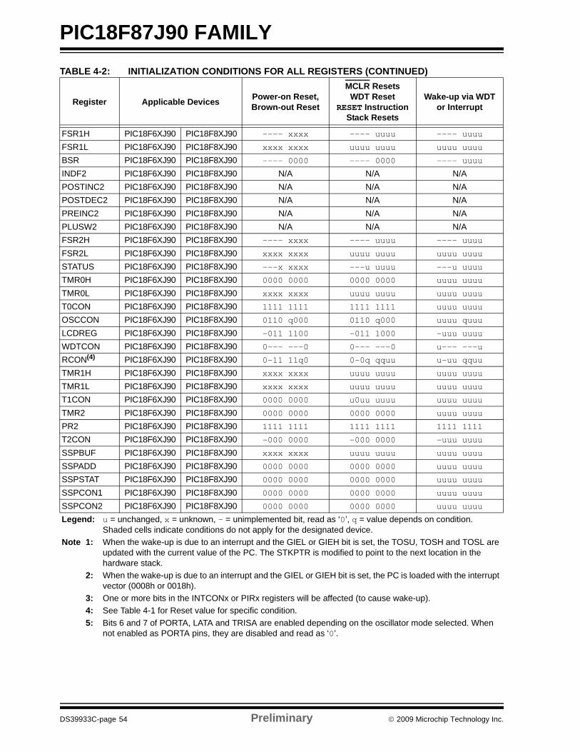
PIC18F87J90 FAMILY
DS39933C-page 54 Preliminary © 2009 Microchip Technology Inc.
FSR1H PIC18F6XJ90 PIC18F8XJ90 ---- xxxx ---- uuuu ---- uuuu
FSR1L PIC18F6XJ90 PIC18F8XJ90 xxxx xxxx uuuu uuuu uuuu uuuu
BSR PIC18F6XJ90 PIC18F8XJ90 ---- 0000 ---- 0000 ---- uuuu
INDF2 PIC18F6XJ90 PIC18F8XJ90 N/A N/A N/APOSTINC2 PIC18F6XJ90 PIC18F8XJ90 N/A N/A N/APOSTDEC2 PIC18F6XJ90 PIC18F8XJ90 N/A N/A N/APREINC2 PIC18F6XJ90 PIC18F8XJ90 N/A N/A N/APLUSW2 PIC18F6XJ90 PIC18F8XJ90 N/A N/A N/AFSR2H PIC18F6XJ90 PIC18F8XJ90 ---- xxxx ---- uuuu ---- uuuu
FSR2L PIC18F6XJ90 PIC18F8XJ90 xxxx xxxx uuuu uuuu uuuu uuuu
STATUS PIC18F6XJ90 PIC18F8XJ90 ---x xxxx ---u uuuu ---u uuuu
TMR0H PIC18F6XJ90 PIC18F8XJ90 0000 0000 0000 0000 uuuu uuuu
TMR0L PIC18F6XJ90 PIC18F8XJ90 xxxx xxxx uuuu uuuu uuuu uuuu
T0CON PIC18F6XJ90 PIC18F8XJ90 1111 1111 1111 1111 uuuu uuuu
OSCCON PIC18F6XJ90 PIC18F8XJ90 0110 q000 0110 q000 uuuu quuu
LCDREG PIC18F6XJ90 PIC18F8XJ90 -011 1100 -011 1000 -uuu uuuu
WDTCON PIC18F6XJ90 PIC18F8XJ90 0--- ---0 0--- ---0 u--- ---u
RCON(4) PIC18F6XJ90 PIC18F8XJ90 0-11 11q0 0-0q qquu u-uu qquu
TMR1H PIC18F6XJ90 PIC18F8XJ90 xxxx xxxx uuuu uuuu uuuu uuuu
TMR1L PIC18F6XJ90 PIC18F8XJ90 xxxx xxxx uuuu uuuu uuuu uuuu
T1CON PIC18F6XJ90 PIC18F8XJ90 0000 0000 u0uu uuuu uuuu uuuu
TMR2 PIC18F6XJ90 PIC18F8XJ90 0000 0000 0000 0000 uuuu uuuu
PR2 PIC18F6XJ90 PIC18F8XJ90 1111 1111 1111 1111 1111 1111
T2CON PIC18F6XJ90 PIC18F8XJ90 -000 0000 -000 0000 -uuu uuuu
SSPBUF PIC18F6XJ90 PIC18F8XJ90 xxxx xxxx uuuu uuuu uuuu uuuu
SSPADD PIC18F6XJ90 PIC18F8XJ90 0000 0000 0000 0000 uuuu uuuu
SSPSTAT PIC18F6XJ90 PIC18F8XJ90 0000 0000 0000 0000 uuuu uuuu
SSPCON1 PIC18F6XJ90 PIC18F8XJ90 0000 0000 0000 0000 uuuu uuuu
SSPCON2 PIC18F6XJ90 PIC18F8XJ90 0000 0000 0000 0000 uuuu uuuu
TABLE 4-2: INITIALIZATION CONDITIONS FOR ALL REGISTERS (CONTINUED)
Register Applicable Devices Power-on Reset,Brown-out Reset
MCLR ResetsWDT Reset
RESET InstructionStack Resets
Wake-up via WDT or Interrupt
Legend: u = unchanged, x = unknown, - = unimplemented bit, read as ‘0’, q = value depends on condition.Shaded cells indicate conditions do not apply for the designated device.
Note 1: When the wake-up is due to an interrupt and the GIEL or GIEH bit is set, the TOSU, TOSH and TOSL are updated with the current value of the PC. The STKPTR is modified to point to the next location in the hardware stack.
2: When the wake-up is due to an interrupt and the GIEL or GIEH bit is set, the PC is loaded with the interrupt vector (0008h or 0018h).
3: One or more bits in the INTCONx or PIRx registers will be affected (to cause wake-up).4: See Table 4-1 for Reset value for specific condition.5: Bits 6 and 7 of PORTA, LATA and TRISA are enabled depending on the oscillator mode selected. When
not enabled as PORTA pins, they are disabled and read as ‘0’.
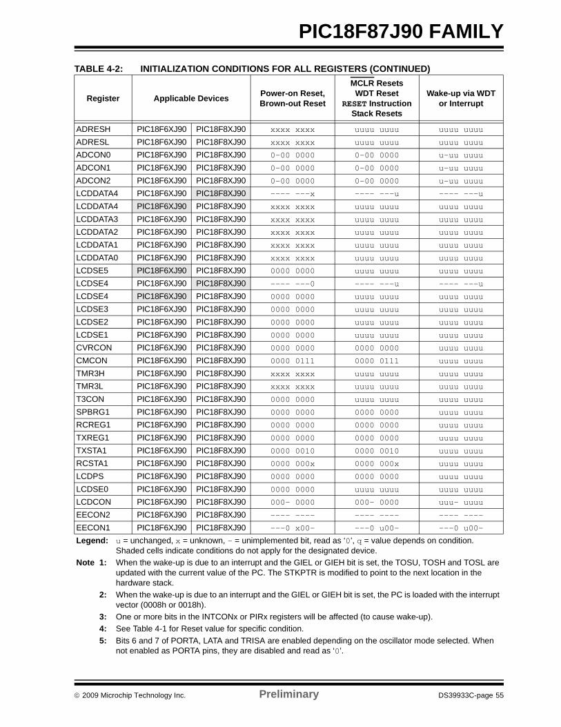
© 2009 Microchip Technology Inc. Preliminary DS39933C-page 55
PIC18F87J90 FAMILY
ADRESH PIC18F6XJ90 PIC18F8XJ90 xxxx xxxx uuuu uuuu uuuu uuuu
ADRESL PIC18F6XJ90 PIC18F8XJ90 xxxx xxxx uuuu uuuu uuuu uuuu
ADCON0 PIC18F6XJ90 PIC18F8XJ90 0-00 0000 0-00 0000 u-uu uuuu
ADCON1 PIC18F6XJ90 PIC18F8XJ90 0-00 0000 0-00 0000 u-uu uuuu
ADCON2 PIC18F6XJ90 PIC18F8XJ90 0-00 0000 0-00 0000 u-uu uuuu
LCDDATA4 PIC18F6XJ90 PIC18F8XJ90 ---- ---x ---- ---u ---- ---u
LCDDATA4 PIC18F6XJ90 PIC18F8XJ90 xxxx xxxx uuuu uuuu uuuu uuuu
LCDDATA3 PIC18F6XJ90 PIC18F8XJ90 xxxx xxxx uuuu uuuu uuuu uuuu
LCDDATA2 PIC18F6XJ90 PIC18F8XJ90 xxxx xxxx uuuu uuuu uuuu uuuu
LCDDATA1 PIC18F6XJ90 PIC18F8XJ90 xxxx xxxx uuuu uuuu uuuu uuuu
LCDDATA0 PIC18F6XJ90 PIC18F8XJ90 xxxx xxxx uuuu uuuu uuuu uuuu
LCDSE5 PIC18F6XJ90 PIC18F8XJ90 0000 0000 uuuu uuuu uuuu uuuu
LCDSE4 PIC18F6XJ90 PIC18F8XJ90 ---- ---0 ---- ---u ---- ---u
LCDSE4 PIC18F6XJ90 PIC18F8XJ90 0000 0000 uuuu uuuu uuuu uuuu
LCDSE3 PIC18F6XJ90 PIC18F8XJ90 0000 0000 uuuu uuuu uuuu uuuu
LCDSE2 PIC18F6XJ90 PIC18F8XJ90 0000 0000 uuuu uuuu uuuu uuuu
LCDSE1 PIC18F6XJ90 PIC18F8XJ90 0000 0000 uuuu uuuu uuuu uuuu
CVRCON PIC18F6XJ90 PIC18F8XJ90 0000 0000 0000 0000 uuuu uuuu
CMCON PIC18F6XJ90 PIC18F8XJ90 0000 0111 0000 0111 uuuu uuuu
TMR3H PIC18F6XJ90 PIC18F8XJ90 xxxx xxxx uuuu uuuu uuuu uuuu
TMR3L PIC18F6XJ90 PIC18F8XJ90 xxxx xxxx uuuu uuuu uuuu uuuu
T3CON PIC18F6XJ90 PIC18F8XJ90 0000 0000 uuuu uuuu uuuu uuuu
SPBRG1 PIC18F6XJ90 PIC18F8XJ90 0000 0000 0000 0000 uuuu uuuu
RCREG1 PIC18F6XJ90 PIC18F8XJ90 0000 0000 0000 0000 uuuu uuuu
TXREG1 PIC18F6XJ90 PIC18F8XJ90 0000 0000 0000 0000 uuuu uuuu
TXSTA1 PIC18F6XJ90 PIC18F8XJ90 0000 0010 0000 0010 uuuu uuuu
RCSTA1 PIC18F6XJ90 PIC18F8XJ90 0000 000x 0000 000x uuuu uuuu
LCDPS PIC18F6XJ90 PIC18F8XJ90 0000 0000 0000 0000 uuuu uuuu
LCDSE0 PIC18F6XJ90 PIC18F8XJ90 0000 0000 uuuu uuuu uuuu uuuu
LCDCON PIC18F6XJ90 PIC18F8XJ90 000- 0000 000- 0000 uuu- uuuu
EECON2 PIC18F6XJ90 PIC18F8XJ90 ---- ---- ---- ---- ---- ----
EECON1 PIC18F6XJ90 PIC18F8XJ90 ---0 x00- ---0 u00- ---0 u00-
TABLE 4-2: INITIALIZATION CONDITIONS FOR ALL REGISTERS (CONTINUED)
Register Applicable Devices Power-on Reset,Brown-out Reset
MCLR ResetsWDT Reset
RESET InstructionStack Resets
Wake-up via WDT or Interrupt
Legend: u = unchanged, x = unknown, - = unimplemented bit, read as ‘0’, q = value depends on condition.Shaded cells indicate conditions do not apply for the designated device.
Note 1: When the wake-up is due to an interrupt and the GIEL or GIEH bit is set, the TOSU, TOSH and TOSL are updated with the current value of the PC. The STKPTR is modified to point to the next location in the hardware stack.
2: When the wake-up is due to an interrupt and the GIEL or GIEH bit is set, the PC is loaded with the interrupt vector (0008h or 0018h).
3: One or more bits in the INTCONx or PIRx registers will be affected (to cause wake-up).4: See Table 4-1 for Reset value for specific condition.5: Bits 6 and 7 of PORTA, LATA and TRISA are enabled depending on the oscillator mode selected. When
not enabled as PORTA pins, they are disabled and read as ‘0’.
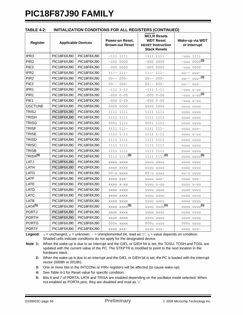
PIC18F87J90 FAMILY
DS39933C-page 56 Preliminary © 2009 Microchip Technology Inc.
IPR3 PIC18F6XJ90 PIC18F8XJ90 -111 1111 -111 1111 -uuu 1111
PIR3 PIC18F6XJ90 PIC18F8XJ90 -000 0000 -000 0000 -uuu 0000(3)
PIE3 PIC18F6XJ90 PIC18F8XJ90 -000 0000 -000 0000 -uuu 0000
IPR2 PIC18F6XJ90 PIC18F8XJ90 11-- 111- 11-- 111- uu-- uuu-
PIR2 PIC18F6XJ90 PIC18F8XJ90 00-- 000- 00-- 000- uu-- uuu-(3)
PIE2 PIC18F6XJ90 PIC18F8XJ90 00-- 000- 00-- 000- uu-- uuu-
IPR1 PIC18F6XJ90 PIC18F8XJ90 -111 1-11 -111 1-11 -uuu u-uu
PIR1 PIC18F6XJ90 PIC18F8XJ90 -000 0-00 -000 0-00 -uuu u-uu(3)
PIE1 PIC18F6XJ90 PIC18F8XJ90 -000 0-00 -000 0-00 -uuu u-uu
OSCTUNE PIC18F6XJ90 PIC18F8XJ90 0000 0000 0000 0000 uuuu uuuu
TRISJ PIC18F6XJ90 PIC18F8XJ90 1111 1111 1111 1111 uuuu uuuu
TRISH PIC18F6XJ90 PIC18F8XJ90 1111 1111 1111 1111 uuuu uuuu
TRISG PIC18F6XJ90 PIC18F8XJ90 0001 1111 0001 1111 uuuu uuuu
TRISF PIC18F6XJ90 PIC18F8XJ90 1111 111- 1111 111- uuuu uuu-
TRISE PIC18F6XJ90 PIC18F8XJ90 1111 1-11 1111 1-11 uuuu u-uu
TRISD PIC18F6XJ90 PIC18F8XJ90 1111 1111 1111 1111 uuuu uuuu
TRISC PIC18F6XJ90 PIC18F8XJ90 1111 1111 1111 1111 uuuu uuuu
TRISB PIC18F6XJ90 PIC18F8XJ90 1111 1111 1111 1111 uuuu uuuu
TRISA(5) PIC18F6XJ90 PIC18F8XJ90 1111 1111(5) 1111 1111(5) uuuu uuuu(5)
LATJ PIC18F6XJ90 PIC18F8XJ90 xxxx xxxx uuuu uuuu uuuu uuuu
LATH PIC18F6XJ90 PIC18F8XJ90 xxxx xxxx uuuu uuuu uuuu uuuu
LATG PIC18F6XJ90 PIC18F8XJ90 00-x xxxx 00-u uuuu uu-u uuuu
LATF PIC18F6XJ90 PIC18F8XJ90 xxxx xxx- uuuu uuu- uuuu uuu-
LATE PIC18F6XJ90 PIC18F8XJ90 xxxx x-xx uuuu u-uu uuuu u-uu
LATD PIC18F6XJ90 PIC18F8XJ90 xxxx xxxx uuuu uuuu uuuu uuuu
LATC PIC18F6XJ90 PIC18F8XJ90 xxxx xxxx uuuu uuuu uuuu uuuu
LATB PIC18F6XJ90 PIC18F8XJ90 xxxx xxxx uuuu uuuu uuuu uuuu
LATA(5) PIC18F6XJ90 PIC18F8XJ90 xxxx xxxx(5) uuuu uuuu(5) uuuu uuuu(5)
PORTJ PIC18F6XJ90 PIC18F8XJ90 xxxx xxxx uuuu uuuu uuuu uuuu
PORTH PIC18F6XJ90 PIC18F8XJ90 xxxx xxxx uuuu uuuu uuuu uuuu
PORTG PIC18F6XJ90 PIC18F8XJ90 000x xxxx 000u uuuu 000u uuuu
PORTF PIC18F6XJ90 PIC18F8XJ90 xxxx xxx- uuuu uuu- uuuu uuu-
TABLE 4-2: INITIALIZATION CONDITIONS FOR ALL REGISTERS (CONTINUED)
Register Applicable Devices Power-on Reset,Brown-out Reset
MCLR ResetsWDT Reset
RESET InstructionStack Resets
Wake-up via WDT or Interrupt
Legend: u = unchanged, x = unknown, - = unimplemented bit, read as ‘0’, q = value depends on condition.Shaded cells indicate conditions do not apply for the designated device.
Note 1: When the wake-up is due to an interrupt and the GIEL or GIEH bit is set, the TOSU, TOSH and TOSL are updated with the current value of the PC. The STKPTR is modified to point to the next location in the hardware stack.
2: When the wake-up is due to an interrupt and the GIEL or GIEH bit is set, the PC is loaded with the interrupt vector (0008h or 0018h).
3: One or more bits in the INTCONx or PIRx registers will be affected (to cause wake-up).4: See Table 4-1 for Reset value for specific condition.5: Bits 6 and 7 of PORTA, LATA and TRISA are enabled depending on the oscillator mode selected. When
not enabled as PORTA pins, they are disabled and read as ‘0’.
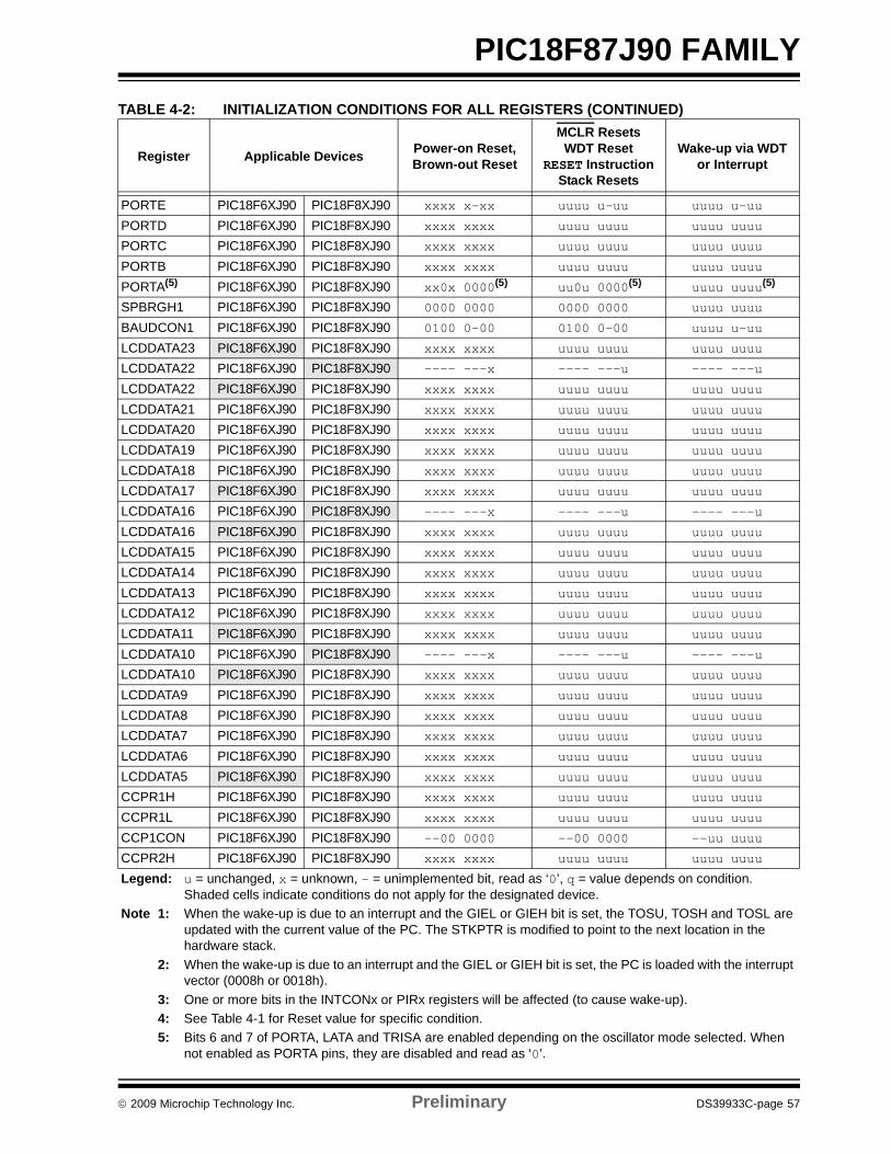
© 2009 Microchip Technology Inc. Preliminary DS39933C-page 57
PIC18F87J90 FAMILY
PORTE PIC18F6XJ90 PIC18F8XJ90 xxxx x-xx uuuu u-uu uuuu u-uu
PORTD PIC18F6XJ90 PIC18F8XJ90 xxxx xxxx uuuu uuuu uuuu uuuu
PORTC PIC18F6XJ90 PIC18F8XJ90 xxxx xxxx uuuu uuuu uuuu uuuu
PORTB PIC18F6XJ90 PIC18F8XJ90 xxxx xxxx uuuu uuuu uuuu uuuu
PORTA(5) PIC18F6XJ90 PIC18F8XJ90 xx0x 0000(5) uu0u 0000(5) uuuu uuuu(5)
SPBRGH1 PIC18F6XJ90 PIC18F8XJ90 0000 0000 0000 0000 uuuu uuuu
BAUDCON1 PIC18F6XJ90 PIC18F8XJ90 0100 0-00 0100 0-00 uuuu u-uu
LCDDATA23 PIC18F6XJ90 PIC18F8XJ90 xxxx xxxx uuuu uuuu uuuu uuuu
LCDDATA22 PIC18F6XJ90 PIC18F8XJ90 ---- ---x ---- ---u ---- ---u
LCDDATA22 PIC18F6XJ90 PIC18F8XJ90 xxxx xxxx uuuu uuuu uuuu uuuu
LCDDATA21 PIC18F6XJ90 PIC18F8XJ90 xxxx xxxx uuuu uuuu uuuu uuuu
LCDDATA20 PIC18F6XJ90 PIC18F8XJ90 xxxx xxxx uuuu uuuu uuuu uuuu
LCDDATA19 PIC18F6XJ90 PIC18F8XJ90 xxxx xxxx uuuu uuuu uuuu uuuu
LCDDATA18 PIC18F6XJ90 PIC18F8XJ90 xxxx xxxx uuuu uuuu uuuu uuuu
LCDDATA17 PIC18F6XJ90 PIC18F8XJ90 xxxx xxxx uuuu uuuu uuuu uuuu
LCDDATA16 PIC18F6XJ90 PIC18F8XJ90 ---- ---x ---- ---u ---- ---u
LCDDATA16 PIC18F6XJ90 PIC18F8XJ90 xxxx xxxx uuuu uuuu uuuu uuuu
LCDDATA15 PIC18F6XJ90 PIC18F8XJ90 xxxx xxxx uuuu uuuu uuuu uuuu
LCDDATA14 PIC18F6XJ90 PIC18F8XJ90 xxxx xxxx uuuu uuuu uuuu uuuu
LCDDATA13 PIC18F6XJ90 PIC18F8XJ90 xxxx xxxx uuuu uuuu uuuu uuuu
LCDDATA12 PIC18F6XJ90 PIC18F8XJ90 xxxx xxxx uuuu uuuu uuuu uuuu
LCDDATA11 PIC18F6XJ90 PIC18F8XJ90 xxxx xxxx uuuu uuuu uuuu uuuu
LCDDATA10 PIC18F6XJ90 PIC18F8XJ90 ---- ---x ---- ---u ---- ---u
LCDDATA10 PIC18F6XJ90 PIC18F8XJ90 xxxx xxxx uuuu uuuu uuuu uuuu
LCDDATA9 PIC18F6XJ90 PIC18F8XJ90 xxxx xxxx uuuu uuuu uuuu uuuu
LCDDATA8 PIC18F6XJ90 PIC18F8XJ90 xxxx xxxx uuuu uuuu uuuu uuuu
LCDDATA7 PIC18F6XJ90 PIC18F8XJ90 xxxx xxxx uuuu uuuu uuuu uuuu
LCDDATA6 PIC18F6XJ90 PIC18F8XJ90 xxxx xxxx uuuu uuuu uuuu uuuu
LCDDATA5 PIC18F6XJ90 PIC18F8XJ90 xxxx xxxx uuuu uuuu uuuu uuuu
CCPR1H PIC18F6XJ90 PIC18F8XJ90 xxxx xxxx uuuu uuuu uuuu uuuu
CCPR1L PIC18F6XJ90 PIC18F8XJ90 xxxx xxxx uuuu uuuu uuuu uuuu
CCP1CON PIC18F6XJ90 PIC18F8XJ90 --00 0000 --00 0000 --uu uuuu
CCPR2H PIC18F6XJ90 PIC18F8XJ90 xxxx xxxx uuuu uuuu uuuu uuuu
TABLE 4-2: INITIALIZATION CONDITIONS FOR ALL REGISTERS (CONTINUED)
Register Applicable Devices Power-on Reset,Brown-out Reset
MCLR ResetsWDT Reset
RESET InstructionStack Resets
Wake-up via WDT or Interrupt
Legend: u = unchanged, x = unknown, - = unimplemented bit, read as ‘0’, q = value depends on condition.Shaded cells indicate conditions do not apply for the designated device.
Note 1: When the wake-up is due to an interrupt and the GIEL or GIEH bit is set, the TOSU, TOSH and TOSL are updated with the current value of the PC. The STKPTR is modified to point to the next location in the hardware stack.
2: When the wake-up is due to an interrupt and the GIEL or GIEH bit is set, the PC is loaded with the interrupt vector (0008h or 0018h).
3: One or more bits in the INTCONx or PIRx registers will be affected (to cause wake-up).4: See Table 4-1 for Reset value for specific condition.5: Bits 6 and 7 of PORTA, LATA and TRISA are enabled depending on the oscillator mode selected. When
not enabled as PORTA pins, they are disabled and read as ‘0’.
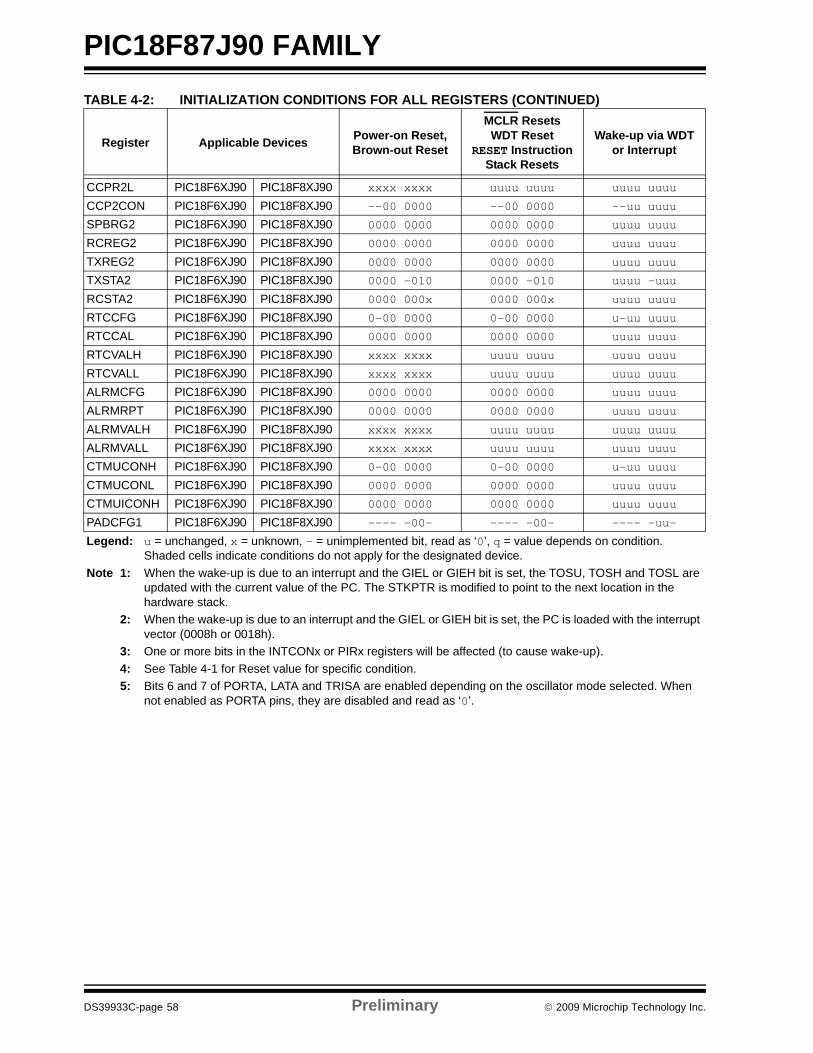
PIC18F87J90 FAMILY
DS39933C-page 58 Preliminary © 2009 Microchip Technology Inc.
CCPR2L PIC18F6XJ90 PIC18F8XJ90 xxxx xxxx uuuu uuuu uuuu uuuu
CCP2CON PIC18F6XJ90 PIC18F8XJ90 --00 0000 --00 0000 --uu uuuu
SPBRG2 PIC18F6XJ90 PIC18F8XJ90 0000 0000 0000 0000 uuuu uuuu
RCREG2 PIC18F6XJ90 PIC18F8XJ90 0000 0000 0000 0000 uuuu uuuu
TXREG2 PIC18F6XJ90 PIC18F8XJ90 0000 0000 0000 0000 uuuu uuuu
TXSTA2 PIC18F6XJ90 PIC18F8XJ90 0000 -010 0000 -010 uuuu -uuu
RCSTA2 PIC18F6XJ90 PIC18F8XJ90 0000 000x 0000 000x uuuu uuuu
RTCCFG PIC18F6XJ90 PIC18F8XJ90 0-00 0000 0-00 0000 u-uu uuuu
RTCCAL PIC18F6XJ90 PIC18F8XJ90 0000 0000 0000 0000 uuuu uuuu
RTCVALH PIC18F6XJ90 PIC18F8XJ90 xxxx xxxx uuuu uuuu uuuu uuuu
RTCVALL PIC18F6XJ90 PIC18F8XJ90 xxxx xxxx uuuu uuuu uuuu uuuu
ALRMCFG PIC18F6XJ90 PIC18F8XJ90 0000 0000 0000 0000 uuuu uuuu
ALRMRPT PIC18F6XJ90 PIC18F8XJ90 0000 0000 0000 0000 uuuu uuuu
ALRMVALH PIC18F6XJ90 PIC18F8XJ90 xxxx xxxx uuuu uuuu uuuu uuuu
ALRMVALL PIC18F6XJ90 PIC18F8XJ90 xxxx xxxx uuuu uuuu uuuu uuuu
CTMUCONH PIC18F6XJ90 PIC18F8XJ90 0-00 0000 0-00 0000 u-uu uuuu
CTMUCONL PIC18F6XJ90 PIC18F8XJ90 0000 0000 0000 0000 uuuu uuuu
CTMUICONH PIC18F6XJ90 PIC18F8XJ90 0000 0000 0000 0000 uuuu uuuu
PADCFG1 PIC18F6XJ90 PIC18F8XJ90 ---- -00- ---- -00- ---- -uu-
TABLE 4-2: INITIALIZATION CONDITIONS FOR ALL REGISTERS (CONTINUED)
Register Applicable Devices Power-on Reset,Brown-out Reset
MCLR ResetsWDT Reset
RESET InstructionStack Resets
Wake-up via WDT or Interrupt
Legend: u = unchanged, x = unknown, - = unimplemented bit, read as ‘0’, q = value depends on condition.Shaded cells indicate conditions do not apply for the designated device.
Note 1: When the wake-up is due to an interrupt and the GIEL or GIEH bit is set, the TOSU, TOSH and TOSL are updated with the current value of the PC. The STKPTR is modified to point to the next location in the hardware stack.
2: When the wake-up is due to an interrupt and the GIEL or GIEH bit is set, the PC is loaded with the interrupt vector (0008h or 0018h).
3: One or more bits in the INTCONx or PIRx registers will be affected (to cause wake-up).4: See Table 4-1 for Reset value for specific condition.5: Bits 6 and 7 of PORTA, LATA and TRISA are enabled depending on the oscillator mode selected. When
not enabled as PORTA pins, they are disabled and read as ‘0’.
© 2009 Microchip Technology Inc. Preliminary DS39933C-page 59
PIC18F87J90 FAMILY
5.0 MEMORY ORGANIZATIONThere are two types of memory in PIC18 Flashmicrocontroller devices:
• Program Memory• Data RAM
As Harvard architecture devices, the data and programmemories use separate busses; this allows forconcurrent access of the two memory spaces.
Additional detailed information on the operation of theFlash program memory is provided in Section 6.0“Flash Program Memory”.
5.1 Program Memory OrganizationPIC18 microcontrollers implement a 21-bit programcounter which is capable of addressing a 2-Mbyteprogram memory space. Accessing a location betweenthe upper boundary of the physically implementedmemory and the 2-Mbyte address will return all ‘0’s (aNOP instruction).
The entire PIC18F87J90 family offers a range ofon-chip Flash program memory sizes, from 64 Kbytes(up to 16,384 single-word instructions) to 128 Kbytes(65,536 single-word instructions). The programmemory maps for individual family members are shownin Figure 5-1.
FIGURE 5-1: MEMORY MAPS FOR PIC18F87J90 FAMILY DEVICES
Note: Sizes of memory areas are not to scale. Sizes of program memory areas are enhanced to show detail.
UnimplementedRead as ‘0’
UnimplementedRead as ‘0’
000000h
1FFFFFh
01FFFFh
00FFFFh
PC<20:0>
Stack Level 1•
Stack Level 31
••
CALL, CALLW, RCALL,RETURN, RETFIE, RETLW,
21
Use
r Mem
ory
Spac
e
On-ChipMemory
On-ChipMemory
ADDULNK, SUBULNK
Config. Words
Config. Words
PIC18FX6J90 PIC18FX7J90
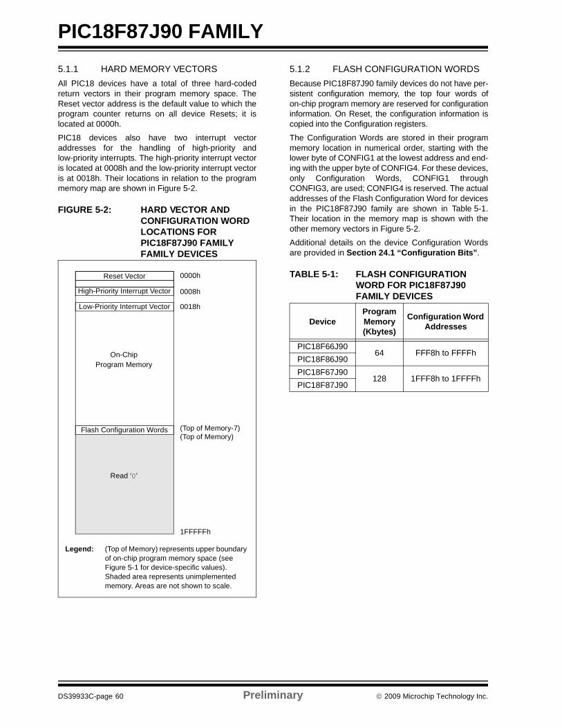
PIC18F87J90 FAMILY
DS39933C-page 60 Preliminary © 2009 Microchip Technology Inc.
5.1.1 HARD MEMORY VECTORSAll PIC18 devices have a total of three hard-codedreturn vectors in their program memory space. TheReset vector address is the default value to which theprogram counter returns on all device Resets; it islocated at 0000h.
PIC18 devices also have two interrupt vectoraddresses for the handling of high-priority andlow-priority interrupts. The high-priority interrupt vectoris located at 0008h and the low-priority interrupt vectoris at 0018h. Their locations in relation to the programmemory map are shown in Figure 5-2.
FIGURE 5-2: HARD VECTOR AND CONFIGURATION WORD LOCATIONS FOR PIC18F87J90 FAMILY FAMILY DEVICES
5.1.2 FLASH CONFIGURATION WORDSBecause PIC18F87J90 family devices do not have per-sistent configuration memory, the top four words ofon-chip program memory are reserved for configurationinformation. On Reset, the configuration information iscopied into the Configuration registers.
The Configuration Words are stored in their programmemory location in numerical order, starting with thelower byte of CONFIG1 at the lowest address and end-ing with the upper byte of CONFIG4. For these devices,only Configuration Words, CONFIG1 throughCONFIG3, are used; CONFIG4 is reserved. The actualaddresses of the Flash Configuration Word for devicesin the PIC18F87J90 family are shown in Table 5-1.Their location in the memory map is shown with theother memory vectors in Figure 5-2.
Additional details on the device Configuration Wordsare provided in Section 24.1 “Configuration Bits”.
TABLE 5-1: FLASH CONFIGURATION WORD FOR PIC18F87J90 FAMILY DEVICES
Reset Vector
Low-Priority Interrupt Vector
0000h
0018h
On-ChipProgram Memory
High-Priority Interrupt Vector 0008h
1FFFFFh
(Top of Memory)(Top of Memory-7)Flash Configuration Words
Read ‘0’
Legend: (Top of Memory) represents upper boundary of on-chip program memory space (see Figure 5-1 for device-specific values). Shaded area represents unimplemented memory. Areas are not shown to scale.
DeviceProgram Memory (Kbytes)
Configuration Word Addresses
PIC18F66J9064 FFF8h to FFFFh
PIC18F86J90PIC18F67J90
128 1FFF8h to 1FFFFhPIC18F87J90
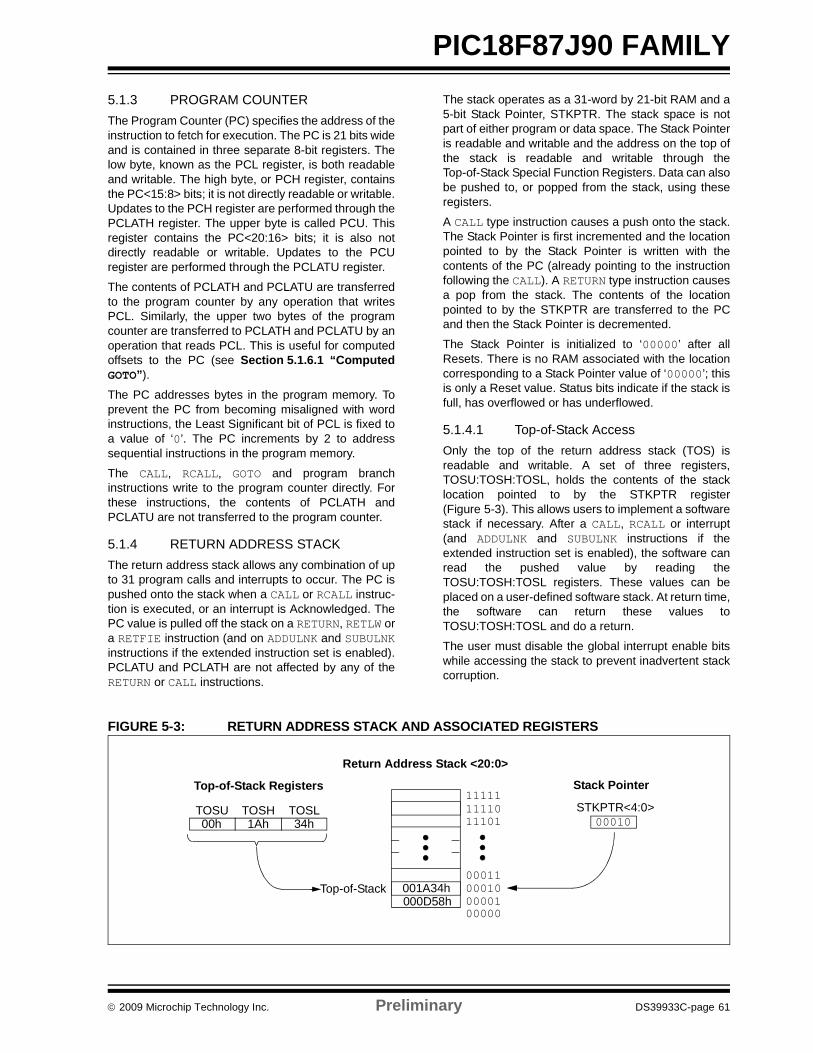
© 2009 Microchip Technology Inc. Preliminary DS39933C-page 61
PIC18F87J90 FAMILY5.1.3 PROGRAM COUNTERThe Program Counter (PC) specifies the address of theinstruction to fetch for execution. The PC is 21 bits wideand is contained in three separate 8-bit registers. Thelow byte, known as the PCL register, is both readableand writable. The high byte, or PCH register, containsthe PC<15:8> bits; it is not directly readable or writable.Updates to the PCH register are performed through thePCLATH register. The upper byte is called PCU. Thisregister contains the PC<20:16> bits; it is also notdirectly readable or writable. Updates to the PCUregister are performed through the PCLATU register.
The contents of PCLATH and PCLATU are transferredto the program counter by any operation that writesPCL. Similarly, the upper two bytes of the programcounter are transferred to PCLATH and PCLATU by anoperation that reads PCL. This is useful for computedoffsets to the PC (see Section 5.1.6.1 “ComputedGOTO”).
The PC addresses bytes in the program memory. Toprevent the PC from becoming misaligned with wordinstructions, the Least Significant bit of PCL is fixed toa value of ‘0’. The PC increments by 2 to addresssequential instructions in the program memory.
The CALL, RCALL, GOTO and program branchinstructions write to the program counter directly. Forthese instructions, the contents of PCLATH andPCLATU are not transferred to the program counter.
5.1.4 RETURN ADDRESS STACKThe return address stack allows any combination of upto 31 program calls and interrupts to occur. The PC ispushed onto the stack when a CALL or RCALL instruc-tion is executed, or an interrupt is Acknowledged. ThePC value is pulled off the stack on a RETURN, RETLW ora RETFIE instruction (and on ADDULNK and SUBULNKinstructions if the extended instruction set is enabled).PCLATU and PCLATH are not affected by any of theRETURN or CALL instructions.
The stack operates as a 31-word by 21-bit RAM and a5-bit Stack Pointer, STKPTR. The stack space is notpart of either program or data space. The Stack Pointeris readable and writable and the address on the top ofthe stack is readable and writable through theTop-of-Stack Special Function Registers. Data can alsobe pushed to, or popped from the stack, using theseregisters.
A CALL type instruction causes a push onto the stack.The Stack Pointer is first incremented and the locationpointed to by the Stack Pointer is written with thecontents of the PC (already pointing to the instructionfollowing the CALL). A RETURN type instruction causesa pop from the stack. The contents of the locationpointed to by the STKPTR are transferred to the PCand then the Stack Pointer is decremented.
The Stack Pointer is initialized to ‘00000’ after allResets. There is no RAM associated with the locationcorresponding to a Stack Pointer value of ‘00000’; thisis only a Reset value. Status bits indicate if the stack isfull, has overflowed or has underflowed.
5.1.4.1 Top-of-Stack AccessOnly the top of the return address stack (TOS) isreadable and writable. A set of three registers,TOSU:TOSH:TOSL, holds the contents of the stacklocation pointed to by the STKPTR register(Figure 5-3). This allows users to implement a softwarestack if necessary. After a CALL, RCALL or interrupt(and ADDULNK and SUBULNK instructions if theextended instruction set is enabled), the software canread the pushed value by reading theTOSU:TOSH:TOSL registers. These values can beplaced on a user-defined software stack. At return time,the software can return these values toTOSU:TOSH:TOSL and do a return.
The user must disable the global interrupt enable bitswhile accessing the stack to prevent inadvertent stackcorruption.
FIGURE 5-3: RETURN ADDRESS STACK AND ASSOCIATED REGISTERS
00011001A34h
111111111011101
000100000100000
00010
Return Address Stack <20:0>
Top-of-Stack000D58h
TOSLTOSHTOSU34h1Ah00h
STKPTR<4:0>
Top-of-Stack Registers Stack Pointer
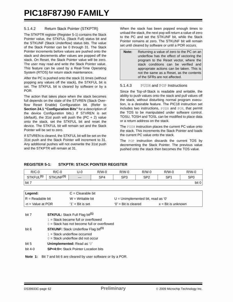
PIC18F87J90 FAMILY
DS39933C-page 62 Preliminary © 2009 Microchip Technology Inc.
5.1.4.2 Return Stack Pointer (STKPTR)The STKPTR register (Register 5-1) contains the StackPointer value, the STKFUL (Stack Full) status bit andthe STKUNF (Stack Underflow) status bits. The valueof the Stack Pointer can be 0 through 31. The StackPointer increments before values are pushed onto thestack and decrements after values are popped off thestack. On Reset, the Stack Pointer value will be zero.The user may read and write the Stack Pointer value.This feature can be used by a Real-Time OperatingSystem (RTOS) for return stack maintenance.
After the PC is pushed onto the stack 31 times (withoutpopping any values off the stack), the STKFUL bit isset. The STKFUL bit is cleared by software or by aPOR.
The action that takes place when the stack becomesfull depends on the state of the STVREN (Stack Over-flow Reset Enable) Configuration bit. (Refer toSection 24.1 “Configuration Bits” for a description ofthe device Configuration bits.) If STVREN is set(default), the 31st push will push the (PC + 2) valueonto the stack, set the STKFUL bit and reset thedevice. The STKFUL bit will remain set and the StackPointer will be set to zero.
If STVREN is cleared, the STKFUL bit will be set on the31st push and the Stack Pointer will increment to 31.Any additional pushes will not overwrite the 31st pushand the STKPTR will remain at 31.
When the stack has been popped enough times tounload the stack, the next pop will return a value of zeroto the PC and set the STKUNF bit, while the StackPointer remains at zero. The STKUNF bit will remainset until cleared by software or until a POR occurs.
5.1.4.3 PUSH and POP InstructionsSince the Top-of-Stack is readable and writable, theability to push values onto the stack and pull values offthe stack, without disturbing normal program execu-tion, is a desirable feature. The PIC18 instruction setincludes two instructions, PUSH and POP, that permitthe TOS to be manipulated under software control.TOSU, TOSH and TOSL can be modified to place dataor a return address on the stack.
The PUSH instruction places the current PC value ontothe stack. This increments the Stack Pointer and loadsthe current PC value onto the stack.
The POP instruction discards the current TOS bydecrementing the Stack Pointer. The previous valuepushed onto the stack then becomes the TOS value.
Note: Returning a value of zero to the PC on anunderflow has the effect of vectoring theprogram to the Reset vector, where thestack conditions can be verified andappropriate actions can be taken. This isnot the same as a Reset, as the contentsof the SFRs are not affected.
REGISTER 5-1: STKPTR: STACK POINTER REGISTER
R/C-0 R/C-0 U-0 R/W-0 R/W-0 R/W-0 R/W-0 R/W-0STKFUL(1) STKUNF(1) — SP4 SP3 SP2 SP1 SP0
bit 7 bit 0
Legend: C = Clearable bitR = Readable bit W = Writable bit U = Unimplemented bit, read as ‘0’-n = Value at POR ‘1’ = Bit is set ‘0’ = Bit is cleared x = Bit is unknown
bit 7 STKFUL: Stack Full Flag bit(1)
1 = Stack became full or overflowed 0 = Stack has not become full or overflowed
bit 6 STKUNF: Stack Underflow Flag bit(1)
1 = Stack underflow occurred 0 = Stack underflow did not occur
bit 5 Unimplemented: Read as ‘0’bit 4-0 SP<4:0>: Stack Pointer Location bits
Note 1: Bit 7 and bit 6 are cleared by user software or by a POR.
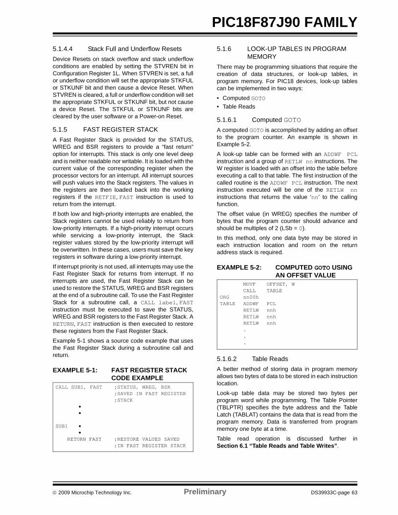
© 2009 Microchip Technology Inc. Preliminary DS39933C-page 63
PIC18F87J90 FAMILY5.1.4.4 Stack Full and Underflow ResetsDevice Resets on stack overflow and stack underflowconditions are enabled by setting the STVREN bit inConfiguration Register 1L. When STVREN is set, a fullor underflow condition will set the appropriate STKFULor STKUNF bit and then cause a device Reset. WhenSTVREN is cleared, a full or underflow condition will setthe appropriate STKFUL or STKUNF bit, but not causea device Reset. The STKFUL or STKUNF bits arecleared by the user software or a Power-on Reset.
5.1.5 FAST REGISTER STACKA Fast Register Stack is provided for the STATUS,WREG and BSR registers to provide a “fast return”option for interrupts. This stack is only one level deepand is neither readable nor writable. It is loaded with thecurrent value of the corresponding register when theprocessor vectors for an interrupt. All interrupt sourceswill push values into the Stack registers. The values inthe registers are then loaded back into the workingregisters if the RETFIE, FAST instruction is used toreturn from the interrupt.
If both low and high-priority interrupts are enabled, theStack registers cannot be used reliably to return fromlow-priority interrupts. If a high-priority interrupt occurswhile servicing a low-priority interrupt, the Stackregister values stored by the low-priority interrupt willbe overwritten. In these cases, users must save the keyregisters in software during a low-priority interrupt.
If interrupt priority is not used, all interrupts may use theFast Register Stack for returns from interrupt. If nointerrupts are used, the Fast Register Stack can beused to restore the STATUS, WREG and BSR registersat the end of a subroutine call. To use the Fast RegisterStack for a subroutine call, a CALL label, FASTinstruction must be executed to save the STATUS,WREG and BSR registers to the Fast Register Stack. ARETURN, FAST instruction is then executed to restorethese registers from the Fast Register Stack.
Example 5-1 shows a source code example that usesthe Fast Register Stack during a subroutine call andreturn.
EXAMPLE 5-1: FAST REGISTER STACK CODE EXAMPLE
5.1.6 LOOK-UP TABLES IN PROGRAM MEMORY
There may be programming situations that require thecreation of data structures, or look-up tables, inprogram memory. For PIC18 devices, look-up tablescan be implemented in two ways:
• Computed GOTO • Table Reads
5.1.6.1 Computed GOTOA computed GOTO is accomplished by adding an offsetto the program counter. An example is shown inExample 5-2.
A look-up table can be formed with an ADDWF PCLinstruction and a group of RETLW nn instructions. TheW register is loaded with an offset into the table beforeexecuting a call to that table. The first instruction of thecalled routine is the ADDWF PCL instruction. The nextinstruction executed will be one of the RETLW nninstructions that returns the value ‘nn’ to the callingfunction.
The offset value (in WREG) specifies the number ofbytes that the program counter should advance andshould be multiples of 2 (LSb = 0).
In this method, only one data byte may be stored ineach instruction location and room on the returnaddress stack is required.
EXAMPLE 5-2: COMPUTED GOTO USING AN OFFSET VALUE
5.1.6.2 Table ReadsA better method of storing data in program memoryallows two bytes of data to be stored in each instructionlocation.
Look-up table data may be stored two bytes perprogram word while programming. The Table Pointer(TBLPTR) specifies the byte address and the TableLatch (TABLAT) contains the data that is read from theprogram memory. Data is transferred from programmemory one byte at a time.
Table read operation is discussed further inSection 6.1 “Table Reads and Table Writes”.
CALL SUB1, FAST ;STATUS, WREG, BSR;SAVED IN FAST REGISTER;STACK
••
SUB1 ••
RETURN FAST ;RESTORE VALUES SAVED;IN FAST REGISTER STACK
MOVF OFFSET, WCALL TABLE
ORG nn00hTABLE ADDWF PCL
RETLW nnhRETLW nnhRETLW nnh...
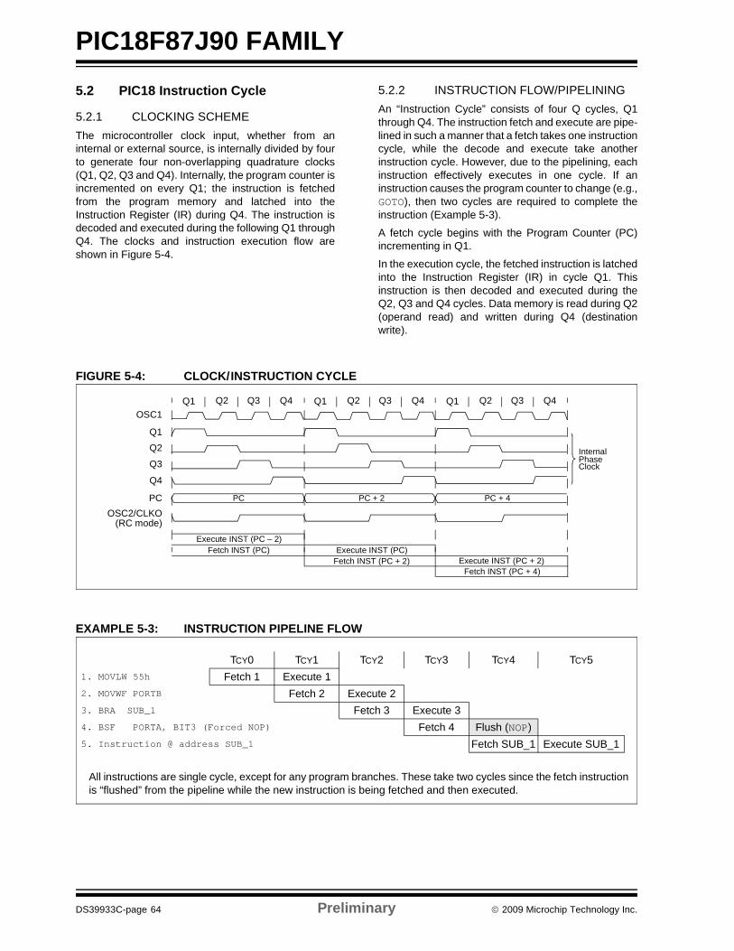
PIC18F87J90 FAMILY
DS39933C-page 64 Preliminary © 2009 Microchip Technology Inc.
5.2 PIC18 Instruction Cycle
5.2.1 CLOCKING SCHEMEThe microcontroller clock input, whether from aninternal or external source, is internally divided by fourto generate four non-overlapping quadrature clocks(Q1, Q2, Q3 and Q4). Internally, the program counter isincremented on every Q1; the instruction is fetchedfrom the program memory and latched into theInstruction Register (IR) during Q4. The instruction isdecoded and executed during the following Q1 throughQ4. The clocks and instruction execution flow areshown in Figure 5-4.
5.2.2 INSTRUCTION FLOW/PIPELININGAn “Instruction Cycle” consists of four Q cycles, Q1through Q4. The instruction fetch and execute are pipe-lined in such a manner that a fetch takes one instructioncycle, while the decode and execute take anotherinstruction cycle. However, due to the pipelining, eachinstruction effectively executes in one cycle. If aninstruction causes the program counter to change (e.g.,GOTO), then two cycles are required to complete theinstruction (Example 5-3).
A fetch cycle begins with the Program Counter (PC)incrementing in Q1.
In the execution cycle, the fetched instruction is latchedinto the Instruction Register (IR) in cycle Q1. Thisinstruction is then decoded and executed during theQ2, Q3 and Q4 cycles. Data memory is read during Q2(operand read) and written during Q4 (destinationwrite).
FIGURE 5-4: CLOCK/INSTRUCTION CYCLE
EXAMPLE 5-3: INSTRUCTION PIPELINE FLOW
Q1 Q2 Q3 Q4 Q1 Q2 Q3 Q4 Q1 Q2 Q3 Q4OSC1
Q1
Q2
Q3
Q4
PCOSC2/CLKO
(RC mode)
PC PC + 2 PC + 4
Fetch INST (PC)Execute INST (PC – 2)
Fetch INST (PC + 2)Execute INST (PC)
Fetch INST (PC + 4)Execute INST (PC + 2)
InternalPhaseClock
All instructions are single cycle, except for any program branches. These take two cycles since the fetch instructionis “flushed” from the pipeline while the new instruction is being fetched and then executed.
TCY0 TCY1 TCY2 TCY3 TCY4 TCY51. MOVLW 55h Fetch 1 Execute 12. MOVWF PORTB Fetch 2 Execute 23. BRA SUB_1 Fetch 3 Execute 34. BSF PORTA, BIT3 (Forced NOP) Fetch 4 Flush (NOP)5. Instruction @ address SUB_1 Fetch SUB_1 Execute SUB_1
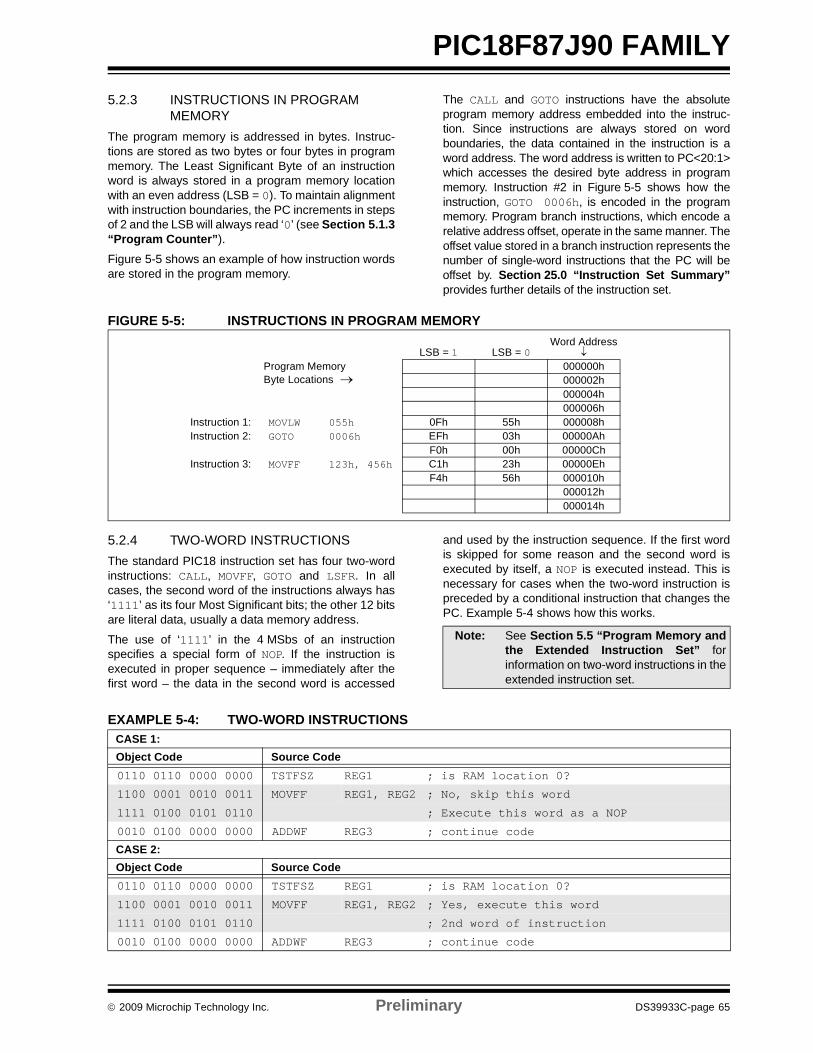
© 2009 Microchip Technology Inc. Preliminary DS39933C-page 65
PIC18F87J90 FAMILY5.2.3 INSTRUCTIONS IN PROGRAM
MEMORYThe program memory is addressed in bytes. Instruc-tions are stored as two bytes or four bytes in programmemory. The Least Significant Byte of an instructionword is always stored in a program memory locationwith an even address (LSB = 0). To maintain alignmentwith instruction boundaries, the PC increments in stepsof 2 and the LSB will always read ‘0’ (see Section 5.1.3“Program Counter”).
Figure 5-5 shows an example of how instruction wordsare stored in the program memory.
The CALL and GOTO instructions have the absoluteprogram memory address embedded into the instruc-tion. Since instructions are always stored on wordboundaries, the data contained in the instruction is aword address. The word address is written to PC<20:1>which accesses the desired byte address in programmemory. Instruction #2 in Figure 5-5 shows how theinstruction, GOTO 0006h, is encoded in the programmemory. Program branch instructions, which encode arelative address offset, operate in the same manner. Theoffset value stored in a branch instruction represents thenumber of single-word instructions that the PC will beoffset by. Section 25.0 “Instruction Set Summary”provides further details of the instruction set.
FIGURE 5-5: INSTRUCTIONS IN PROGRAM MEMORY
5.2.4 TWO-WORD INSTRUCTIONSThe standard PIC18 instruction set has four two-wordinstructions: CALL, MOVFF, GOTO and LSFR. In allcases, the second word of the instructions always has‘1111’ as its four Most Significant bits; the other 12 bitsare literal data, usually a data memory address.
The use of ‘1111’ in the 4 MSbs of an instructionspecifies a special form of NOP. If the instruction isexecuted in proper sequence – immediately after thefirst word – the data in the second word is accessed
and used by the instruction sequence. If the first wordis skipped for some reason and the second word isexecuted by itself, a NOP is executed instead. This isnecessary for cases when the two-word instruction ispreceded by a conditional instruction that changes thePC. Example 5-4 shows how this works.
EXAMPLE 5-4: TWO-WORD INSTRUCTIONS
Word AddressLSB = 1 LSB = 0 ↓
Program MemoryByte Locations →
000000h000002h000004h000006h
Instruction 1: MOVLW 055h 0Fh 55h 000008hInstruction 2: GOTO 0006h EFh 03h 00000Ah
F0h 00h 00000ChInstruction 3: MOVFF 123h, 456h C1h 23h 00000Eh
F4h 56h 000010h000012h000014h
Note: See Section 5.5 “Program Memory andthe Extended Instruction Set” forinformation on two-word instructions in theextended instruction set.
CASE 1:Object Code Source Code0110 0110 0000 0000 TSTFSZ REG1 ; is RAM location 0?
1100 0001 0010 0011 MOVFF REG1, REG2 ; No, skip this word
1111 0100 0101 0110 ; Execute this word as a NOP
0010 0100 0000 0000 ADDWF REG3 ; continue code
CASE 2:Object Code Source Code0110 0110 0000 0000 TSTFSZ REG1 ; is RAM location 0?
1100 0001 0010 0011 MOVFF REG1, REG2 ; Yes, execute this word
1111 0100 0101 0110 ; 2nd word of instruction
0010 0100 0000 0000 ADDWF REG3 ; continue code
PIC18F87J90 FAMILY
DS39933C-page 66 Preliminary © 2009 Microchip Technology Inc.
5.3 Data Memory Organization
The data memory in PIC18 devices is implemented asstatic RAM. Each register in the data memory has a12-bit address, allowing up to 4,096 bytes of datamemory. The memory space is divided into as many as16 banks that contain 256 bytes each. PIC18FX6J90and PIC18FX7J90 devices implement all 16 completebanks, for a total of 4 Kbytes. Figure 5-6 and Figure 5-7show the data memory organization for the devices.
The data memory contains Special Function Registers(SFRs) and General Purpose Registers (GPRs). TheSFRs are used for control and status of the controllerand peripheral functions, while GPRs are used for datastorage and scratchpad operations in the user’sapplication. Any read of an unimplemented location willread as ‘0’s.
The instruction set and architecture allow operationsacross all banks. The entire data memory may beaccessed by Direct, Indirect or Indexed Addressingmodes. Addressing modes are discussed later in thissection.
To ensure that commonly used registers (select SFRsand select GPRs) can be accessed in a single cycle,PIC18 devices implement an Access Bank. This is a256-byte memory space that provides fast access toselect SFRs and the lower portion of GPR Bank 0 with-out using the BSR. Section 5.3.2 “Access Bank”provides a detailed description of the Access RAM.
5.3.1 BANK SELECT REGISTERLarge areas of data memory require an efficientaddressing scheme to make rapid access to anyaddress possible. Ideally, this means that an entireaddress does not need to be provided for each read orwrite operation. For PIC18 devices, this is accom-plished with a RAM banking scheme. This divides thememory space into 16 contiguous banks of 256 bytes.Depending on the instruction, each location can beaddressed directly by its full 12-bit address, or an 8-bitlow-order address and a 4-bit Bank Pointer.
Most instructions in the PIC18 instruction set make useof the Bank Pointer, known as the Bank Select Register(BSR). This SFR holds the 4 Most Significant bits of alocation’s address; the instruction itself includes the8 Least Significant bits. Only the four lower bits of theBSR are implemented (BSR<3:0>). The upper four bitsare unused; they will always read ‘0’ and cannot bewritten to. The BSR can be loaded directly by using theMOVLB instruction.
The value of the BSR indicates the bank in datamemory. The 8 bits in the instruction show the locationin the bank and can be thought of as an offset from thebank’s lower boundary. The relationship between theBSR’s value and the bank division in data memory isshown in Figure 5-7.
Since up to 16 registers may share the same low-orderaddress, the user must always be careful to ensure thatthe proper bank is selected before performing a dataread or write. For example, writing what should beprogram data to an 8-bit address of F9h while the BSRis 0Fh, will end up resetting the program counter.
While any bank can be selected, only those banks thatare actually implemented can be read or written to.Writes to unimplemented banks are ignored, whilereads from unimplemented banks will return ‘0’s. Evenso, the STATUS register will still be affected as if theoperation was successful. The data memory map inFigure 5-6 indicates which banks are implemented.
In the core PIC18 instruction set, only the MOVFFinstruction fully specifies the 12-bit address of thesource and target registers. This instruction ignores theBSR completely when it executes. All other instructionsinclude only the low-order address as an operand andmust use either the BSR or the Access Bank to locatetheir target registers.
Note: The operation of some aspects of datamemory are changed when the PIC18extended instruction set is enabled. SeeSection 5.6 “Data Memory and theExtended Instruction Set” for moreinformation.
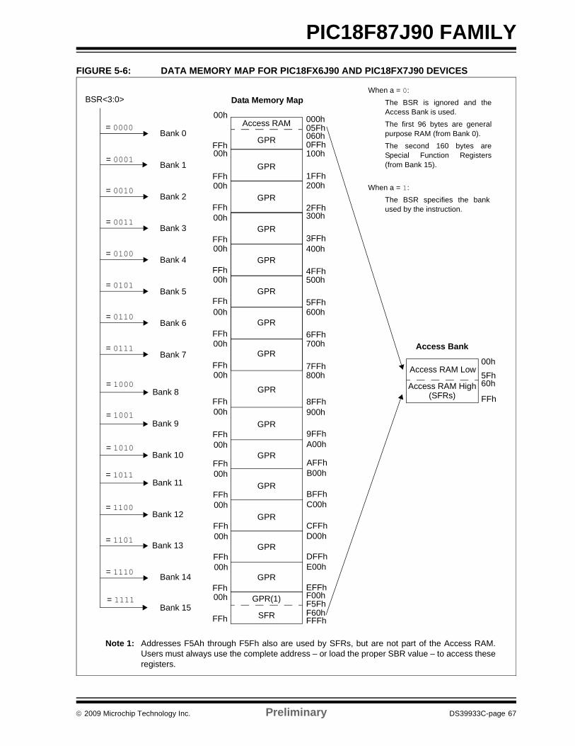
© 2009 Microchip Technology Inc. Preliminary DS39933C-page 67
PIC18F87J90 FAMILYFIGURE 5-6: DATA MEMORY MAP FOR PIC18FX6J90 AND PIC18FX7J90 DEVICES
00h5Fh60h
FFh
Access Bank
When a = 0: The BSR is ignored and theAccess Bank is used.The first 96 bytes are generalpurpose RAM (from Bank 0). The second 160 bytes areSpecial Function Registers(from Bank 15).
When a = 1: The BSR specifies the bankused by the instruction.
Access RAM High
Access RAM Low
(SFRs)
Bank 0
Bank 1
Bank 14
Bank 15
Data Memory MapBSR<3:0>
= 0000
= 0001
= 1111
060h05Fh
F60hFFFh
F5FhF00hEFFh
1FFh
100h0FFh
000hAccess RAM
FFh
00h
FFh
00h
FFh
00h
GPR
GPR
SFR
Bank 2= 0010
2FFh
200h
Bank 3
FFh
00hGPR
FFh
= 0011
GPR(1)
GPR
GPR
GPR
GPR
GPR
4FFh
400h
5FFh
500h
3FFh
300h
FFh
00h
FFh
00h
FFh
00h
FFh
00h
FFh
00h
00h
= 0110
= 0111
= 0101
= 0100Bank 4
Bank 5
Bank 6
Bank 7
Bank 8
= 1110
6FFh
600h
7FFh
700h
800h
Bank 9
Bank 10
Bank 11
Bank 12
Bank 13
8FFh900h
9FFhA00h
AFFhB00h
BFFhC00h
CFFhD00h
DFFhE00h
FFh00h
FFh00h
FFh00h
FFh00h
FFh00h
FFh00h
GPR
GPR
GPR
GPR
GPR
GPR
GPR
Note 1: Addresses F5Ah through F5Fh also are used by SFRs, but are not part of the Access RAM.Users must always use the complete address – or load the proper SBR value – to access theseregisters.
= 1000
= 1001
= 1010
= 1011
= 1100
= 1101
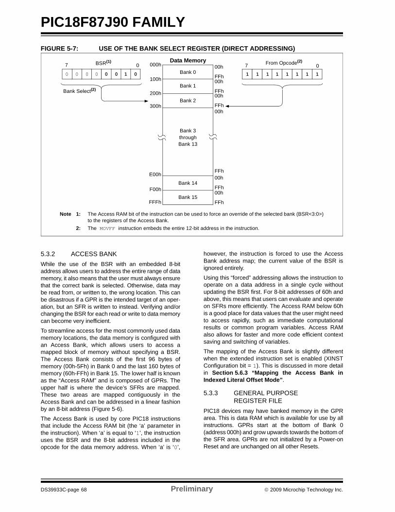
PIC18F87J90 FAMILY
DS39933C-page 68 Preliminary © 2009 Microchip Technology Inc.
FIGURE 5-7: USE OF THE BANK SELECT REGISTER (DIRECT ADDRESSING)
5.3.2 ACCESS BANKWhile the use of the BSR with an embedded 8-bitaddress allows users to address the entire range of datamemory, it also means that the user must always ensurethat the correct bank is selected. Otherwise, data maybe read from, or written to, the wrong location. This canbe disastrous if a GPR is the intended target of an oper-ation, but an SFR is written to instead. Verifying and/orchanging the BSR for each read or write to data memorycan become very inefficient.
To streamline access for the most commonly used datamemory locations, the data memory is configured withan Access Bank, which allows users to access amapped block of memory without specifying a BSR.The Access Bank consists of the first 96 bytes ofmemory (00h-5Fh) in Bank 0 and the last 160 bytes ofmemory (60h-FFh) in Bank 15. The lower half is knownas the “Access RAM” and is composed of GPRs. Theupper half is where the device’s SFRs are mapped.These two areas are mapped contiguously in theAccess Bank and can be addressed in a linear fashionby an 8-bit address (Figure 5-6).
The Access Bank is used by core PIC18 instructionsthat include the Access RAM bit (the ‘a’ parameter inthe instruction). When ‘a’ is equal to ‘1’, the instructionuses the BSR and the 8-bit address included in theopcode for the data memory address. When ‘a’ is ‘0’,
however, the instruction is forced to use the AccessBank address map; the current value of the BSR isignored entirely.
Using this “forced” addressing allows the instruction tooperate on a data address in a single cycle withoutupdating the BSR first. For 8-bit addresses of 60h andabove, this means that users can evaluate and operateon SFRs more efficiently. The Access RAM below 60his a good place for data values that the user might needto access rapidly, such as immediate computationalresults or common program variables. Access RAMalso allows for faster and more code efficient contextsaving and switching of variables.
The mapping of the Access Bank is slightly differentwhen the extended instruction set is enabled (XINSTConfiguration bit = 1). This is discussed in more detailin Section 5.6.3 “Mapping the Access Bank inIndexed Literal Offset Mode”.
5.3.3 GENERAL PURPOSE REGISTER FILE
PIC18 devices may have banked memory in the GPRarea. This is data RAM which is available for use by allinstructions. GPRs start at the bottom of Bank 0(address 000h) and grow upwards towards the bottom ofthe SFR area. GPRs are not initialized by a Power-onReset and are unchanged on all other Resets.
Note 1: The Access RAM bit of the instruction can be used to force an override of the selected bank (BSR<3:0>) to the registers of the Access Bank.
2: The MOVFF instruction embeds the entire 12-bit address in the instruction.
Data Memory
Bank Select(2)
7 0From Opcode(2)
0 0 0 0
000h
100h
200h
300h
F00h
E00h
FFFh
Bank 0
Bank 1
Bank 2
Bank 14
Bank 15
00h
FFh00h
FFh00h
FFh
00h
FFh00h
FFh
00h
FFh
Bank 3throughBank 13
0 0 1 0 1 1 1 1 1 1 1 1
7 0BSR(1)
1 1 1 1 1 1 1 1
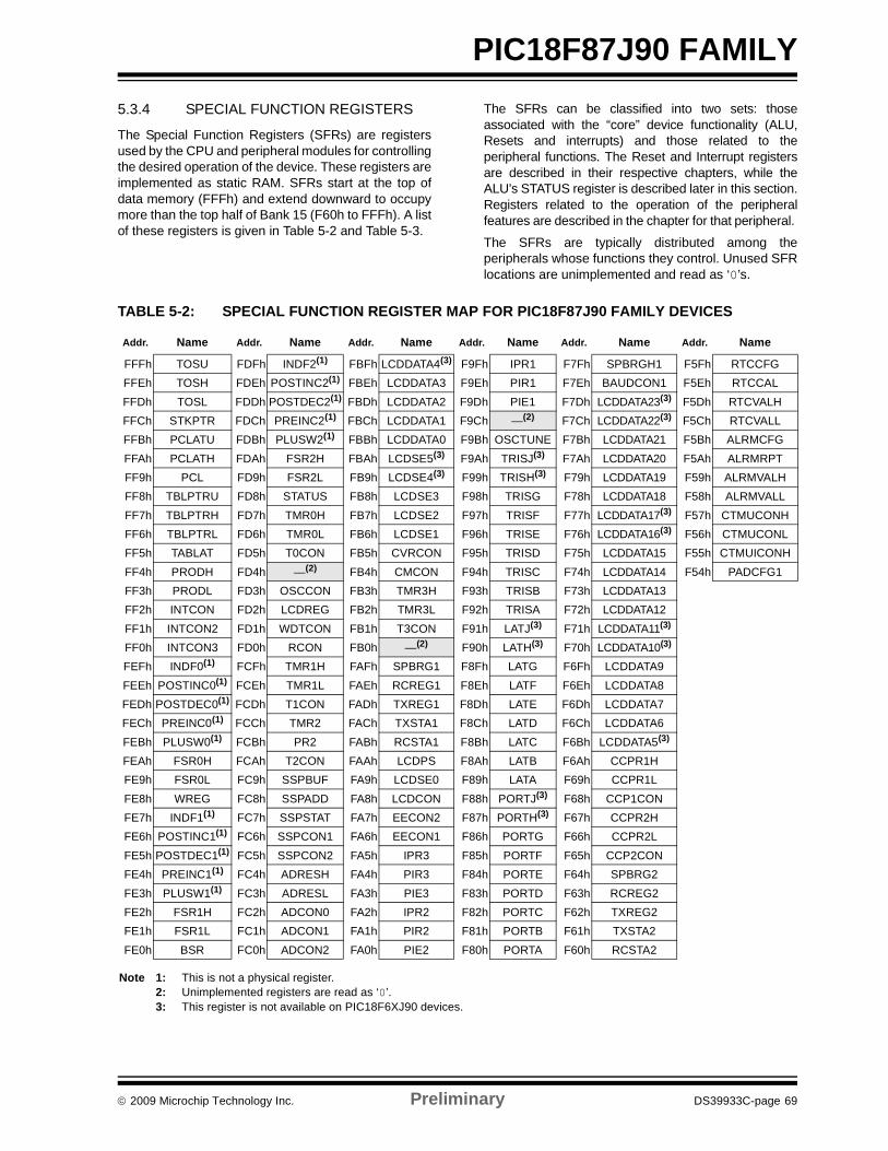
© 2009 Microchip Technology Inc. Preliminary DS39933C-page 69
PIC18F87J90 FAMILY5.3.4 SPECIAL FUNCTION REGISTERS
The Special Function Registers (SFRs) are registersused by the CPU and peripheral modules for controllingthe desired operation of the device. These registers areimplemented as static RAM. SFRs start at the top ofdata memory (FFFh) and extend downward to occupymore than the top half of Bank 15 (F60h to FFFh). A listof these registers is given in Table 5-2 and Table 5-3.
The SFRs can be classified into two sets: thoseassociated with the “core” device functionality (ALU,Resets and interrupts) and those related to theperipheral functions. The Reset and Interrupt registersare described in their respective chapters, while theALU’s STATUS register is described later in this section.Registers related to the operation of the peripheralfeatures are described in the chapter for that peripheral.
The SFRs are typically distributed among theperipherals whose functions they control. Unused SFRlocations are unimplemented and read as ‘0’s.
TABLE 5-2: SPECIAL FUNCTION REGISTER MAP FOR PIC18F87J90 FAMILY DEVICES
Addr. Name Addr. Name Addr. Name Addr. Name Addr. Name Addr. Name
FFFh TOSU FDFh INDF2(1) FBFh LCDDATA4(3) F9Fh IPR1 F7Fh SPBRGH1 F5Fh RTCCFGFFEh TOSH FDEh POSTINC2(1) FBEh LCDDATA3 F9Eh PIR1 F7Eh BAUDCON1 F5Eh RTCCALFFDh TOSL FDDh POSTDEC2(1) FBDh LCDDATA2 F9Dh PIE1 F7Dh LCDDATA23(3) F5Dh RTCVALHFFCh STKPTR FDCh PREINC2(1) FBCh LCDDATA1 F9Ch —(2) F7Ch LCDDATA22(3) F5Ch RTCVALLFFBh PCLATU FDBh PLUSW2(1) FBBh LCDDATA0 F9Bh OSCTUNE F7Bh LCDDATA21 F5Bh ALRMCFGFFAh PCLATH FDAh FSR2H FBAh LCDSE5(3) F9Ah TRISJ(3) F7Ah LCDDATA20 F5Ah ALRMRPTFF9h PCL FD9h FSR2L FB9h LCDSE4(3) F99h TRISH(3) F79h LCDDATA19 F59h ALRMVALHFF8h TBLPTRU FD8h STATUS FB8h LCDSE3 F98h TRISG F78h LCDDATA18 F58h ALRMVALLFF7h TBLPTRH FD7h TMR0H FB7h LCDSE2 F97h TRISF F77h LCDDATA17(3) F57h CTMUCONHFF6h TBLPTRL FD6h TMR0L FB6h LCDSE1 F96h TRISE F76h LCDDATA16(3) F56h CTMUCONLFF5h TABLAT FD5h T0CON FB5h CVRCON F95h TRISD F75h LCDDATA15 F55h CTMUICONHFF4h PRODH FD4h —(2) FB4h CMCON F94h TRISC F74h LCDDATA14 F54h PADCFG1FF3h PRODL FD3h OSCCON FB3h TMR3H F93h TRISB F73h LCDDATA13FF2h INTCON FD2h LCDREG FB2h TMR3L F92h TRISA F72h LCDDATA12FF1h INTCON2 FD1h WDTCON FB1h T3CON F91h LATJ(3) F71h LCDDATA11(3)
FF0h INTCON3 FD0h RCON FB0h —(2) F90h LATH(3) F70h LCDDATA10(3)
FEFh INDF0(1) FCFh TMR1H FAFh SPBRG1 F8Fh LATG F6Fh LCDDATA9FEEh POSTINC0(1) FCEh TMR1L FAEh RCREG1 F8Eh LATF F6Eh LCDDATA8FEDh POSTDEC0(1) FCDh T1CON FADh TXREG1 F8Dh LATE F6Dh LCDDATA7FECh PREINC0(1) FCCh TMR2 FACh TXSTA1 F8Ch LATD F6Ch LCDDATA6FEBh PLUSW0(1) FCBh PR2 FABh RCSTA1 F8Bh LATC F6Bh LCDDATA5(3)
FEAh FSR0H FCAh T2CON FAAh LCDPS F8Ah LATB F6Ah CCPR1HFE9h FSR0L FC9h SSPBUF FA9h LCDSE0 F89h LATA F69h CCPR1LFE8h WREG FC8h SSPADD FA8h LCDCON F88h PORTJ(3) F68h CCP1CONFE7h INDF1(1) FC7h SSPSTAT FA7h EECON2 F87h PORTH(3) F67h CCPR2HFE6h POSTINC1(1) FC6h SSPCON1 FA6h EECON1 F86h PORTG F66h CCPR2LFE5h POSTDEC1(1) FC5h SSPCON2 FA5h IPR3 F85h PORTF F65h CCP2CONFE4h PREINC1(1) FC4h ADRESH FA4h PIR3 F84h PORTE F64h SPBRG2FE3h PLUSW1(1) FC3h ADRESL FA3h PIE3 F83h PORTD F63h RCREG2 FE2h FSR1H FC2h ADCON0 FA2h IPR2 F82h PORTC F62h TXREG2 FE1h FSR1L FC1h ADCON1 FA1h PIR2 F81h PORTB F61h TXSTA2FE0h BSR FC0h ADCON2 FA0h PIE2 F80h PORTA F60h RCSTA2
Note 1: This is not a physical register.2: Unimplemented registers are read as ‘0’.3: This register is not available on PIC18F6XJ90 devices.
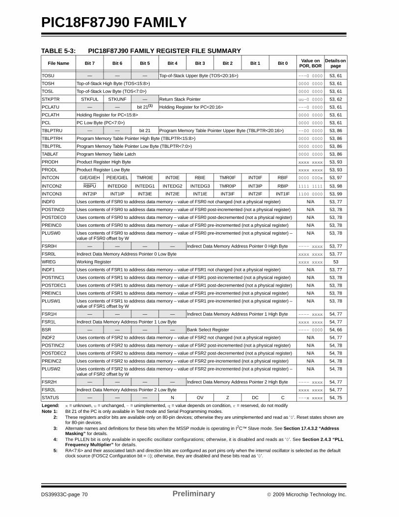
PIC18F87J90 FAMILY
DS39933C-page 70 Preliminary © 2009 Microchip Technology Inc.
TABLE 5-3: PIC18F87J90 FAMILY REGISTER FILE SUMMARY
File Name Bit 7 Bit 6 Bit 5 Bit 4 Bit 3 Bit 2 Bit 1 Bit 0 Value on POR, BOR
Details on page
TOSU — — — Top-of-Stack Upper Byte (TOS<20:16>) ---0 0000 53, 61
TOSH Top-of-Stack High Byte (TOS<15:8>) 0000 0000 53, 61
TOSL Top-of-Stack Low Byte (TOS<7:0>) 0000 0000 53, 61
STKPTR STKFUL STKUNF — Return Stack Pointer uu-0 0000 53, 62
PCLATU — — bit 21(1) Holding Register for PC<20:16> ---0 0000 53, 61
PCLATH Holding Register for PC<15:8> 0000 0000 53, 61
PCL PC Low Byte (PC<7:0>) 0000 0000 53, 61
TBLPTRU — — bit 21 Program Memory Table Pointer Upper Byte (TBLPTR<20:16>) --00 0000 53, 86
TBLPTRH Program Memory Table Pointer High Byte (TBLPTR<15:8>) 0000 0000 53, 86
TBLPTRL Program Memory Table Pointer Low Byte (TBLPTR<7:0>) 0000 0000 53, 86
TABLAT Program Memory Table Latch 0000 0000 53, 86
PRODH Product Register High Byte xxxx xxxx 53, 93
PRODL Product Register Low Byte xxxx xxxx 53, 93
INTCON GIE/GIEH PEIE/GIEL TMR0IE INT0IE RBIE TMR0IF INT0IF RBIF 0000 000x 53, 97
INTCON2 RBPU INTEDG0 INTEDG1 INTEDG2 INTEDG3 TMR0IP INT3IP RBIP 1111 1111 53, 98
INTCON3 INT2IP INT1IP INT3IE INT2IE INT1IE INT3IF INT2IF INT1IF 1100 0000 53, 99
INDF0 Uses contents of FSR0 to address data memory – value of FSR0 not changed (not a physical register) N/A 53, 77
POSTINC0 Uses contents of FSR0 to address data memory – value of FSR0 post-incremented (not a physical register) N/A 53, 78
POSTDEC0 Uses contents of FSR0 to address data memory – value of FSR0 post-decremented (not a physical register) N/A 53, 78
PREINC0 Uses contents of FSR0 to address data memory – value of FSR0 pre-incremented (not a physical register) N/A 53, 78
PLUSW0 Uses contents of FSR0 to address data memory – value of FSR0 pre-incremented (not a physical register) – value of FSR0 offset by W
N/A 53, 78
FSR0H — — — — Indirect Data Memory Address Pointer 0 High Byte ---- xxxx 53, 77
FSR0L Indirect Data Memory Address Pointer 0 Low Byte xxxx xxxx 53, 77
WREG Working Register xxxx xxxx 53
INDF1 Uses contents of FSR1 to address data memory – value of FSR1 not changed (not a physical register) N/A 53, 77
POSTINC1 Uses contents of FSR1 to address data memory – value of FSR1 post-incremented (not a physical register) N/A 53, 78
POSTDEC1 Uses contents of FSR1 to address data memory – value of FSR1 post-decremented (not a physical register) N/A 53, 78
PREINC1 Uses contents of FSR1 to address data memory – value of FSR1 pre-incremented (not a physical register) N/A 53, 78
PLUSW1 Uses contents of FSR1 to address data memory – value of FSR1 pre-incremented (not a physical register) – value of FSR1 offset by W
N/A 53, 78
FSR1H — — — — Indirect Data Memory Address Pointer 1 High Byte ---- xxxx 54, 77
FSR1L Indirect Data Memory Address Pointer 1 Low Byte xxxx xxxx 54, 77
BSR — — — — Bank Select Register ---- 0000 54, 66
INDF2 Uses contents of FSR2 to address data memory – value of FSR2 not changed (not a physical register) N/A 54, 77
POSTINC2 Uses contents of FSR2 to address data memory – value of FSR2 post-incremented (not a physical register) N/A 54, 78
POSTDEC2 Uses contents of FSR2 to address data memory – value of FSR2 post-decremented (not a physical register) N/A 54, 78
PREINC2 Uses contents of FSR2 to address data memory – value of FSR2 pre-incremented (not a physical register) N/A 54, 78
PLUSW2 Uses contents of FSR2 to address data memory – value of FSR2 pre-incremented (not a physical register) – value of FSR2 offset by W
N/A 54, 78
FSR2H — — — — Indirect Data Memory Address Pointer 2 High Byte ---- xxxx 54, 77
FSR2L Indirect Data Memory Address Pointer 2 Low Byte xxxx xxxx 54, 77
STATUS — — — N OV Z DC C ---x xxxx 54, 75
Legend: x = unknown, u = unchanged, - = unimplemented, q = value depends on condition, r = reserved, do not modifyNote 1: Bit 21 of the PC is only available in Test mode and Serial Programming modes.
2: These registers and/or bits are available only on 80-pin devices; otherwise they are unimplemented and read as ‘0’. Reset states shown are for 80-pin devices.
3: Alternate names and definitions for these bits when the MSSP module is operating in I2C™ Slave mode. See Section 17.4.3.2 “Address Masking” for details.
4: The PLLEN bit is only available in specific oscillator configurations; otherwise, it is disabled and reads as ‘0’. See Section 2.4.3 “PLL Frequency Multiplier” for details.
5: RA<7:6> and their associated latch and direction bits are configured as port pins only when the internal oscillator is selected as the default clock source (FOSC2 Configuration bit = 0); otherwise, they are disabled and these bits read as ‘0’.
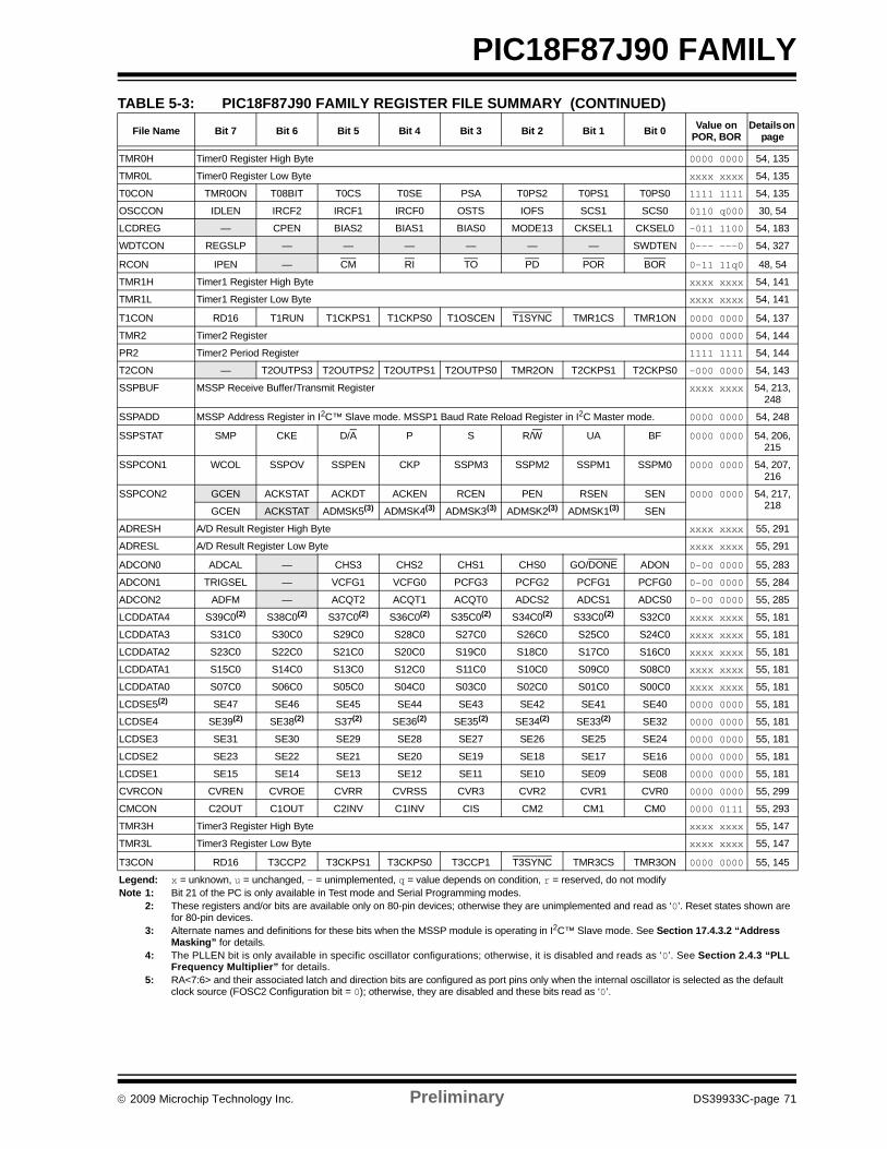
© 2009 Microchip Technology Inc. Preliminary DS39933C-page 71
PIC18F87J90 FAMILY
TMR0H Timer0 Register High Byte 0000 0000 54, 135
TMR0L Timer0 Register Low Byte xxxx xxxx 54, 135
T0CON TMR0ON T08BIT T0CS T0SE PSA T0PS2 T0PS1 T0PS0 1111 1111 54, 135
OSCCON IDLEN IRCF2 IRCF1 IRCF0 OSTS IOFS SCS1 SCS0 0110 q000 30, 54
LCDREG — CPEN BIAS2 BIAS1 BIAS0 MODE13 CKSEL1 CKSEL0 -011 1100 54, 183
WDTCON REGSLP — — — — — — SWDTEN 0--- ---0 54, 327
RCON IPEN — CM RI TO PD POR BOR 0-11 11q0 48, 54
TMR1H Timer1 Register High Byte xxxx xxxx 54, 141
TMR1L Timer1 Register Low Byte xxxx xxxx 54, 141
T1CON RD16 T1RUN T1CKPS1 T1CKPS0 T1OSCEN T1SYNC TMR1CS TMR1ON 0000 0000 54, 137
TMR2 Timer2 Register 0000 0000 54, 144
PR2 Timer2 Period Register 1111 1111 54, 144
T2CON — T2OUTPS3 T2OUTPS2 T2OUTPS1 T2OUTPS0 TMR2ON T2CKPS1 T2CKPS0 -000 0000 54, 143
SSPBUF MSSP Receive Buffer/Transmit Register xxxx xxxx 54, 213, 248
SSPADD MSSP Address Register in I2C™ Slave mode. MSSP1 Baud Rate Reload Register in I2C Master mode. 0000 0000 54, 248
SSPSTAT SMP CKE D/A P S R/W UA BF 0000 0000 54, 206, 215
SSPCON1 WCOL SSPOV SSPEN CKP SSPM3 SSPM2 SSPM1 SSPM0 0000 0000 54, 207, 216
SSPCON2 GCEN ACKSTAT ACKDT ACKEN RCEN PEN RSEN SEN 0000 0000 54, 217, 218GCEN ACKSTAT ADMSK5(3) ADMSK4(3) ADMSK3(3) ADMSK2(3) ADMSK1(3) SEN
ADRESH A/D Result Register High Byte xxxx xxxx 55, 291
ADRESL A/D Result Register Low Byte xxxx xxxx 55, 291
ADCON0 ADCAL — CHS3 CHS2 CHS1 CHS0 GO/DONE ADON 0-00 0000 55, 283
ADCON1 TRIGSEL — VCFG1 VCFG0 PCFG3 PCFG2 PCFG1 PCFG0 0-00 0000 55, 284
ADCON2 ADFM — ACQT2 ACQT1 ACQT0 ADCS2 ADCS1 ADCS0 0-00 0000 55, 285
LCDDATA4 S39C0(2) S38C0(2) S37C0(2) S36C0(2) S35C0(2) S34C0(2) S33C0(2) S32C0 xxxx xxxx 55, 181
LCDDATA3 S31C0 S30C0 S29C0 S28C0 S27C0 S26C0 S25C0 S24C0 xxxx xxxx 55, 181
LCDDATA2 S23C0 S22C0 S21C0 S20C0 S19C0 S18C0 S17C0 S16C0 xxxx xxxx 55, 181
LCDDATA1 S15C0 S14C0 S13C0 S12C0 S11C0 S10C0 S09C0 S08C0 xxxx xxxx 55, 181
LCDDATA0 S07C0 S06C0 S05C0 S04C0 S03C0 S02C0 S01C0 S00C0 xxxx xxxx 55, 181
LCDSE5(2) SE47 SE46 SE45 SE44 SE43 SE42 SE41 SE40 0000 0000 55, 181
LCDSE4 SE39(2) SE38(2) S37(2) SE36(2) SE35(2) SE34(2) SE33(2) SE32 0000 0000 55, 181
LCDSE3 SE31 SE30 SE29 SE28 SE27 SE26 SE25 SE24 0000 0000 55, 181
LCDSE2 SE23 SE22 SE21 SE20 SE19 SE18 SE17 SE16 0000 0000 55, 181
LCDSE1 SE15 SE14 SE13 SE12 SE11 SE10 SE09 SE08 0000 0000 55, 181
CVRCON CVREN CVROE CVRR CVRSS CVR3 CVR2 CVR1 CVR0 0000 0000 55, 299
CMCON C2OUT C1OUT C2INV C1INV CIS CM2 CM1 CM0 0000 0111 55, 293
TMR3H Timer3 Register High Byte xxxx xxxx 55, 147
TMR3L Timer3 Register Low Byte xxxx xxxx 55, 147
T3CON RD16 T3CCP2 T3CKPS1 T3CKPS0 T3CCP1 T3SYNC TMR3CS TMR3ON 0000 0000 55, 145
TABLE 5-3: PIC18F87J90 FAMILY REGISTER FILE SUMMARY (CONTINUED)
File Name Bit 7 Bit 6 Bit 5 Bit 4 Bit 3 Bit 2 Bit 1 Bit 0 Value on POR, BOR
Details on page
Legend: x = unknown, u = unchanged, - = unimplemented, q = value depends on condition, r = reserved, do not modifyNote 1: Bit 21 of the PC is only available in Test mode and Serial Programming modes.
2: These registers and/or bits are available only on 80-pin devices; otherwise they are unimplemented and read as ‘0’. Reset states shown are for 80-pin devices.
3: Alternate names and definitions for these bits when the MSSP module is operating in I2C™ Slave mode. See Section 17.4.3.2 “Address Masking” for details.
4: The PLLEN bit is only available in specific oscillator configurations; otherwise, it is disabled and reads as ‘0’. See Section 2.4.3 “PLL Frequency Multiplier” for details.
5: RA<7:6> and their associated latch and direction bits are configured as port pins only when the internal oscillator is selected as the default clock source (FOSC2 Configuration bit = 0); otherwise, they are disabled and these bits read as ‘0’.
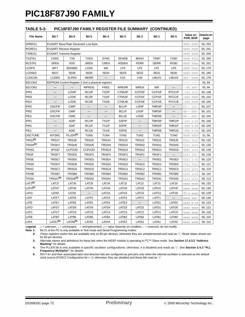
PIC18F87J90 FAMILY
DS39933C-page 72 Preliminary © 2009 Microchip Technology Inc.
SPBRG1 EUSART Baud Rate Generator Low Byte 0000 0000 55, 253
RCREG1 EUSART Receive Register 0000 0000 55, 261
TXREG1 EUSART Transmit Register 0000 0000 55, 259
TXSTA1 CSRC TX9 TXEN SYNC SENDB BRGH TRMT TX9D 0000 0010 55, 250
RCSTA1 SPEN RX9 SREN CREN ADDEN FERR OERR RX9D 0000 000x 55, 251
LCDPS WFT BIASMD LCDA WA LP3 LP2 LP1 LP0 0000 0000 55, 179
LCDSE0 SE07 SE06 SE05 SE04 SE03 SE02 SE01 SE00 0000 0000 55, 180
LCDCON LCDEN SLPEN WERR — CS1 CS0 LMUX1 LMUX0 000- 0000 55, 178
EECON2 EEPROM Control Register 2 (not a physical register) ---- ---- 55, 84
EECON1 — — WPROG FREE WRERR WREN WR — --00 x00- 55, 84
IPR3 — LCDIP RC2IP TX2IP CTMUIP CCP2IP CCP1IP RTCCIP -111 1111 56, 108
PIR3 — LCDIF RC2IF TX2IF CTMUIF CCP2IF CCP1IF RTCCIF -000 0000 56, 102
PIE3 — LCDIE RC2IE TX2IE CTMUIE CCP2IE CCP1IE RTCCIE -000 0000 56, 105
IPR2 OSCFIP CMIP — — BCLIP LVDIP TMR3IP — 11-- 111- 56, 107
PIR2 OSCFIF CMIF — — BCLIF LVDIF TMR3IF — 00-- 000- 56, 101
PIE2 OSCFIE CMIE — — BCLIE LVDIE TMR3IE — 00-- 000- 56, 104
IPR1 — ADIP RC1IP TX1IP SSPIP — TMR2IP TMR1IP -111 1-11 56, 106
PIR1 — ADIF RC1IF TX1IF SSPIF — TMR2IF TMR1IF -000 0-00 56, 100
PIE1 — ADIE RC1IE TX1IE SSPIE — TMR2IE TMR1IE -000 0-00 56, 103
OSCTUNE INTSRC PLLEN(4) TUN5 TUN4 TUN3 TUN2 TUN1 TUN0 0000 0000 31, 56
TRISJ(2) TRISJ7 TRISJ6 TRISJ5 TRISJ4 TRISJ3 TRISJ2 TRISJ1 TRISJ0 1111 1111 56, 132
TRISH(2) TRISH7 TRISH6 TRISH5 TRISH4 TRISH3 TRISH2 TRISH1 TRISH0 1111 1111 56, 130
TRISG SPIOD CCP2OD CCP1OD TRISG4 TRISG3 TRISG2 TRISG1 TRISG0 0001 1111 56, 128
TRISF TRISF7 TRISF6 TRISF5 TRISF4 TRISF3 TRISF2 TRISF1 — 1111 111- 56, 126
TRISE TRISE7 TRISE6 TRISE5 TRISE4 TRISE3 — TRISE1 TRISE0 1111 1-11 56, 123
TRISD TRISD7 TRISD6 TRISD5 TRISD4 TRISD3 TRISD2 TRISD1 TRISD0 1111 1111 56, 121
TRISC TRISC7 TRISC6 TRISC5 TRISC4 TRISC3 TRISC2 TRISC1 TRISC0 1111 1111 56, 119
TRISB TRISB7 TRISB6 TRISB5 TRISB4 TRISB3 TRISB2 TRISB1 TRISB0 1111 1111 56, 116
TRISA TRISA7(5) TRISA6(5) TRISA5 TRISA4 TRISA3 TRISA2 TRISA1 TRISA0 1111 1111 56, 113
LATJ(2) LATJ7 LATJ6 LATJ5 LATJ4 LATJ3 LATJ2 LATJ1 LATJ0 xxxx xxxx 56, 132
LATH(2) LATH7 LATH6 LATH5 LATH4 LATH3 LATH2 LATH1 LATH0 xxxx xxxx 56, 130
LATG U2OD U1OD — LATG4 LATG3 LATG2 LATG1 LATG0 00-x xxxx 56, 128
LATF LATF7 LATF6 LATF5 LATF4 LATF3 LATF2 LATF1 — xxxx xxx- 56, 126
LATE LATE7 LATE6 LATE5 LATE4 LATE3 — LATE1 LATE0 xxxx x-xx 56, 123
LATD LATD7 LATD6 LATD5 LATD4 LATD3 LATD2 LATD1 LATD0 xxxx xxxx 56, 121
LATC LATC7 LATC6 LATC5 LATC4 LATC3 LATC2 LATC1 LATC0 xxxx xxxx 56, 119
LATB LATB7 LATB6 LATB5 LATB4 LATB3 LATB2 LATB1 LATB0 xxxx xxxx 56, 116
LATA LATA7(5) LATA6(5) LATA5 LATA4 LATA3 LATA2 LATA1 LATA0 xxxx xxxx 56, 113
TABLE 5-3: PIC18F87J90 FAMILY REGISTER FILE SUMMARY (CONTINUED)
File Name Bit 7 Bit 6 Bit 5 Bit 4 Bit 3 Bit 2 Bit 1 Bit 0 Value on POR, BOR
Details on page
Legend: x = unknown, u = unchanged, - = unimplemented, q = value depends on condition, r = reserved, do not modifyNote 1: Bit 21 of the PC is only available in Test mode and Serial Programming modes.
2: These registers and/or bits are available only on 80-pin devices; otherwise they are unimplemented and read as ‘0’. Reset states shown are for 80-pin devices.
3: Alternate names and definitions for these bits when the MSSP module is operating in I2C™ Slave mode. See Section 17.4.3.2 “Address Masking” for details.
4: The PLLEN bit is only available in specific oscillator configurations; otherwise, it is disabled and reads as ‘0’. See Section 2.4.3 “PLL Frequency Multiplier” for details.
5: RA<7:6> and their associated latch and direction bits are configured as port pins only when the internal oscillator is selected as the default clock source (FOSC2 Configuration bit = 0); otherwise, they are disabled and these bits read as ‘0’.
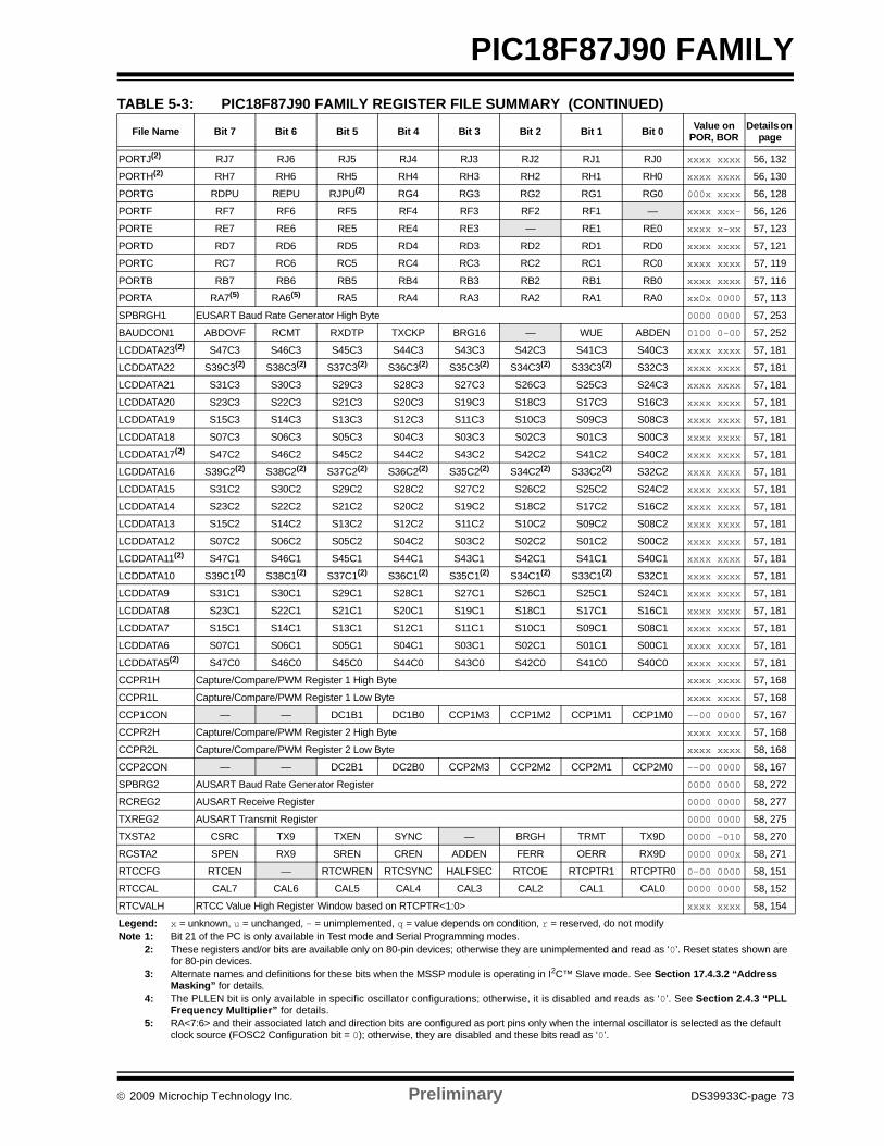
© 2009 Microchip Technology Inc. Preliminary DS39933C-page 73
PIC18F87J90 FAMILY
PORTJ(2) RJ7 RJ6 RJ5 RJ4 RJ3 RJ2 RJ1 RJ0 xxxx xxxx 56, 132
PORTH(2) RH7 RH6 RH5 RH4 RH3 RH2 RH1 RH0 xxxx xxxx 56, 130
PORTG RDPU REPU RJPU(2) RG4 RG3 RG2 RG1 RG0 000x xxxx 56, 128
PORTF RF7 RF6 RF5 RF4 RF3 RF2 RF1 — xxxx xxx- 56, 126
PORTE RE7 RE6 RE5 RE4 RE3 — RE1 RE0 xxxx x-xx 57, 123
PORTD RD7 RD6 RD5 RD4 RD3 RD2 RD1 RD0 xxxx xxxx 57, 121
PORTC RC7 RC6 RC5 RC4 RC3 RC2 RC1 RC0 xxxx xxxx 57, 119
PORTB RB7 RB6 RB5 RB4 RB3 RB2 RB1 RB0 xxxx xxxx 57, 116
PORTA RA7(5) RA6(5) RA5 RA4 RA3 RA2 RA1 RA0 xx0x 0000 57, 113
SPBRGH1 EUSART Baud Rate Generator High Byte 0000 0000 57, 253
BAUDCON1 ABDOVF RCMT RXDTP TXCKP BRG16 — WUE ABDEN 0100 0-00 57, 252
LCDDATA23(2) S47C3 S46C3 S45C3 S44C3 S43C3 S42C3 S41C3 S40C3 xxxx xxxx 57, 181
LCDDATA22 S39C3(2) S38C3(2) S37C3(2) S36C3(2) S35C3(2) S34C3(2) S33C3(2) S32C3 xxxx xxxx 57, 181
LCDDATA21 S31C3 S30C3 S29C3 S28C3 S27C3 S26C3 S25C3 S24C3 xxxx xxxx 57, 181
LCDDATA20 S23C3 S22C3 S21C3 S20C3 S19C3 S18C3 S17C3 S16C3 xxxx xxxx 57, 181
LCDDATA19 S15C3 S14C3 S13C3 S12C3 S11C3 S10C3 S09C3 S08C3 xxxx xxxx 57, 181
LCDDATA18 S07C3 S06C3 S05C3 S04C3 S03C3 S02C3 S01C3 S00C3 xxxx xxxx 57, 181
LCDDATA17(2) S47C2 S46C2 S45C2 S44C2 S43C2 S42C2 S41C2 S40C2 xxxx xxxx 57, 181
LCDDATA16 S39C2(2) S38C2(2) S37C2(2) S36C2(2) S35C2(2) S34C2(2) S33C2(2) S32C2 xxxx xxxx 57, 181
LCDDATA15 S31C2 S30C2 S29C2 S28C2 S27C2 S26C2 S25C2 S24C2 xxxx xxxx 57, 181
LCDDATA14 S23C2 S22C2 S21C2 S20C2 S19C2 S18C2 S17C2 S16C2 xxxx xxxx 57, 181
LCDDATA13 S15C2 S14C2 S13C2 S12C2 S11C2 S10C2 S09C2 S08C2 xxxx xxxx 57, 181
LCDDATA12 S07C2 S06C2 S05C2 S04C2 S03C2 S02C2 S01C2 S00C2 xxxx xxxx 57, 181
LCDDATA11(2) S47C1 S46C1 S45C1 S44C1 S43C1 S42C1 S41C1 S40C1 xxxx xxxx 57, 181
LCDDATA10 S39C1(2) S38C1(2) S37C1(2) S36C1(2) S35C1(2) S34C1(2) S33C1(2) S32C1 xxxx xxxx 57, 181
LCDDATA9 S31C1 S30C1 S29C1 S28C1 S27C1 S26C1 S25C1 S24C1 xxxx xxxx 57, 181
LCDDATA8 S23C1 S22C1 S21C1 S20C1 S19C1 S18C1 S17C1 S16C1 xxxx xxxx 57, 181
LCDDATA7 S15C1 S14C1 S13C1 S12C1 S11C1 S10C1 S09C1 S08C1 xxxx xxxx 57, 181
LCDDATA6 S07C1 S06C1 S05C1 S04C1 S03C1 S02C1 S01C1 S00C1 xxxx xxxx 57, 181
LCDDATA5(2) S47C0 S46C0 S45C0 S44C0 S43C0 S42C0 S41C0 S40C0 xxxx xxxx 57, 181
CCPR1H Capture/Compare/PWM Register 1 High Byte xxxx xxxx 57, 168
CCPR1L Capture/Compare/PWM Register 1 Low Byte xxxx xxxx 57, 168
CCP1CON — — DC1B1 DC1B0 CCP1M3 CCP1M2 CCP1M1 CCP1M0 --00 0000 57, 167
CCPR2H Capture/Compare/PWM Register 2 High Byte xxxx xxxx 57, 168
CCPR2L Capture/Compare/PWM Register 2 Low Byte xxxx xxxx 58, 168
CCP2CON — — DC2B1 DC2B0 CCP2M3 CCP2M2 CCP2M1 CCP2M0 --00 0000 58, 167
SPBRG2 AUSART Baud Rate Generator Register 0000 0000 58, 272
RCREG2 AUSART Receive Register 0000 0000 58, 277
TXREG2 AUSART Transmit Register 0000 0000 58, 275
TXSTA2 CSRC TX9 TXEN SYNC — BRGH TRMT TX9D 0000 -010 58, 270
RCSTA2 SPEN RX9 SREN CREN ADDEN FERR OERR RX9D 0000 000x 58, 271
RTCCFG RTCEN — RTCWREN RTCSYNC HALFSEC RTCOE RTCPTR1 RTCPTR0 0-00 0000 58, 151
RTCCAL CAL7 CAL6 CAL5 CAL4 CAL3 CAL2 CAL1 CAL0 0000 0000 58, 152
RTCVALH RTCC Value High Register Window based on RTCPTR<1:0> xxxx xxxx 58, 154
TABLE 5-3: PIC18F87J90 FAMILY REGISTER FILE SUMMARY (CONTINUED)
File Name Bit 7 Bit 6 Bit 5 Bit 4 Bit 3 Bit 2 Bit 1 Bit 0 Value on POR, BOR
Details on page
Legend: x = unknown, u = unchanged, - = unimplemented, q = value depends on condition, r = reserved, do not modifyNote 1: Bit 21 of the PC is only available in Test mode and Serial Programming modes.
2: These registers and/or bits are available only on 80-pin devices; otherwise they are unimplemented and read as ‘0’. Reset states shown are for 80-pin devices.
3: Alternate names and definitions for these bits when the MSSP module is operating in I2C™ Slave mode. See Section 17.4.3.2 “Address Masking” for details.
4: The PLLEN bit is only available in specific oscillator configurations; otherwise, it is disabled and reads as ‘0’. See Section 2.4.3 “PLL Frequency Multiplier” for details.
5: RA<7:6> and their associated latch and direction bits are configured as port pins only when the internal oscillator is selected as the default clock source (FOSC2 Configuration bit = 0); otherwise, they are disabled and these bits read as ‘0’.
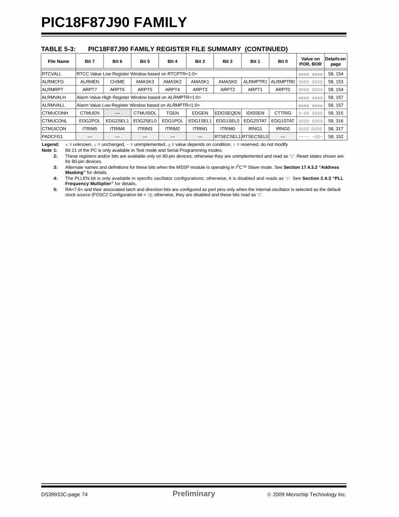
PIC18F87J90 FAMILY
DS39933C-page 74 Preliminary © 2009 Microchip Technology Inc.
RTCVALL RTCC Value Low Register Window based on RTCPTR<1:0> xxxx xxxx 58, 154
ALRMCFG ALRMEN CHIME AMASK3 AMASK2 AMASK1 AMASK0 ALRMPTR1 ALRMPTR0 0000 0000 58, 153
ALRMRPT ARPT7 ARPT6 ARPT5 ARPT4 ARPT3 ARPT2 ARPT1 ARPT0 0000 0000 58, 154
ALRMVALH Alarm Value High Register Window based on ALRMPTR<1:0> xxxx xxxx 58, 157
ALRMVALL Alarm Value Low Register Window based on ALRMPTR<1:0> xxxx xxxx 58, 157
CTMUCONH CTMUEN — CTMUSIDL TGEN EDGEN EDGSEQEN IDISSEN CTTRIG 0-00 0000 58, 315
CTMUCONL EDG2POL EDG2SEL1 EDG2SEL0 EDG1POL EDG1SEL1 EDG1SEL0 EDG2STAT EDG1STAT 0000 0000 58, 316
CTMUICON ITRIM5 ITRIM4 ITRIM3 ITRIM2 ITRIM1 ITRIM0 IRNG1 IRNG0 0000 0000 58, 317
PADCFG1 — — — — — RTSECSEL1 RTSECSEL0 — ---- -00- 58, 152
TABLE 5-3: PIC18F87J90 FAMILY REGISTER FILE SUMMARY (CONTINUED)
File Name Bit 7 Bit 6 Bit 5 Bit 4 Bit 3 Bit 2 Bit 1 Bit 0 Value on POR, BOR
Details on page
Legend: x = unknown, u = unchanged, - = unimplemented, q = value depends on condition, r = reserved, do not modifyNote 1: Bit 21 of the PC is only available in Test mode and Serial Programming modes.
2: These registers and/or bits are available only on 80-pin devices; otherwise they are unimplemented and read as ‘0’. Reset states shown are for 80-pin devices.
3: Alternate names and definitions for these bits when the MSSP module is operating in I2C™ Slave mode. See Section 17.4.3.2 “Address Masking” for details.
4: The PLLEN bit is only available in specific oscillator configurations; otherwise, it is disabled and reads as ‘0’. See Section 2.4.3 “PLL Frequency Multiplier” for details.
5: RA<7:6> and their associated latch and direction bits are configured as port pins only when the internal oscillator is selected as the default clock source (FOSC2 Configuration bit = 0); otherwise, they are disabled and these bits read as ‘0’.
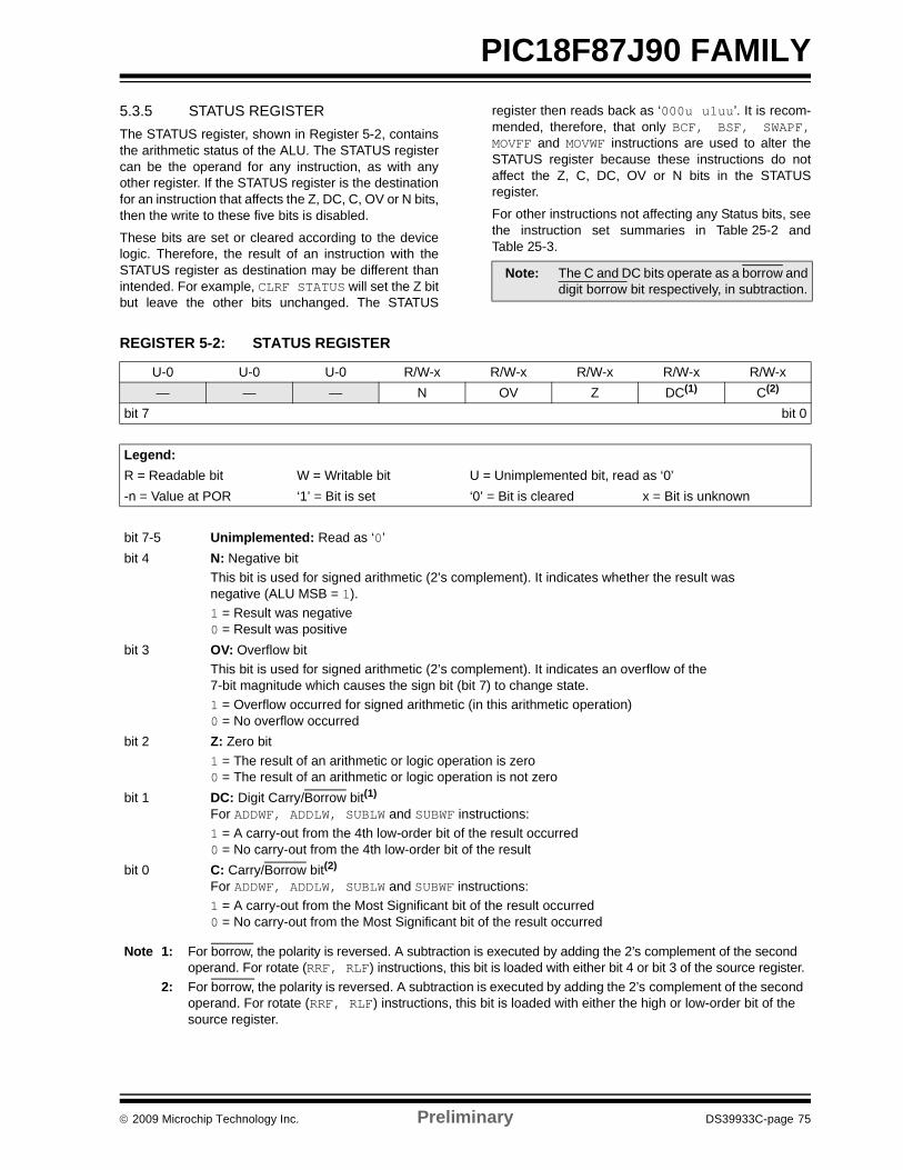
© 2009 Microchip Technology Inc. Preliminary DS39933C-page 75
PIC18F87J90 FAMILY5.3.5 STATUS REGISTERThe STATUS register, shown in Register 5-2, containsthe arithmetic status of the ALU. The STATUS registercan be the operand for any instruction, as with anyother register. If the STATUS register is the destinationfor an instruction that affects the Z, DC, C, OV or N bits,then the write to these five bits is disabled.
These bits are set or cleared according to the devicelogic. Therefore, the result of an instruction with theSTATUS register as destination may be different thanintended. For example, CLRF STATUS will set the Z bitbut leave the other bits unchanged. The STATUS
register then reads back as ‘000u u1uu’. It is recom-mended, therefore, that only BCF, BSF, SWAPF,MOVFF and MOVWF instructions are used to alter theSTATUS register because these instructions do notaffect the Z, C, DC, OV or N bits in the STATUSregister.
For other instructions not affecting any Status bits, seethe instruction set summaries in Table 25-2 andTable 25-3.
Note: The C and DC bits operate as a borrow anddigit borrow bit respectively, in subtraction.
REGISTER 5-2: STATUS REGISTER
U-0 U-0 U-0 R/W-x R/W-x R/W-x R/W-x R/W-x— — — N OV Z DC(1) C(2)
bit 7 bit 0
Legend:R = Readable bit W = Writable bit U = Unimplemented bit, read as ‘0’-n = Value at POR ‘1’ = Bit is set ‘0’ = Bit is cleared x = Bit is unknown
bit 7-5 Unimplemented: Read as ‘0’ bit 4 N: Negative bit
This bit is used for signed arithmetic (2’s complement). It indicates whether the result was negative (ALU MSB = 1).1 = Result was negative 0 = Result was positive
bit 3 OV: Overflow bit This bit is used for signed arithmetic (2’s complement). It indicates an overflow of the 7-bit magnitude which causes the sign bit (bit 7) to change state.1 = Overflow occurred for signed arithmetic (in this arithmetic operation) 0 = No overflow occurred
bit 2 Z: Zero bit 1 = The result of an arithmetic or logic operation is zero 0 = The result of an arithmetic or logic operation is not zero
bit 1 DC: Digit Carry/Borrow bit(1) For ADDWF, ADDLW, SUBLW and SUBWF instructions: 1 = A carry-out from the 4th low-order bit of the result occurred 0 = No carry-out from the 4th low-order bit of the result
bit 0 C: Carry/Borrow bit(2) For ADDWF, ADDLW, SUBLW and SUBWF instructions: 1 = A carry-out from the Most Significant bit of the result occurred 0 = No carry-out from the Most Significant bit of the result occurred
Note 1: For borrow, the polarity is reversed. A subtraction is executed by adding the 2’s complement of the second operand. For rotate (RRF, RLF) instructions, this bit is loaded with either bit 4 or bit 3 of the source register.
2: For borrow, the polarity is reversed. A subtraction is executed by adding the 2’s complement of the second operand. For rotate (RRF, RLF) instructions, this bit is loaded with either the high or low-order bit of the source register.
PIC18F87J90 FAMILY
DS39933C-page 76 Preliminary © 2009 Microchip Technology Inc.
5.4 Data Addressing Modes
While the program memory can be addressed in onlyone way – through the program counter – informationin the data memory space can be addressed in severalways. For most instructions, the addressing mode isfixed. Other instructions may use up to three modes,depending on which operands are used and whether ornot the extended instruction set is enabled.
The addressing modes are:
• Inherent• Literal• Direct• Indirect
An additional addressing mode, Indexed Literal Offset,is available when the extended instruction set isenabled (XINST Configuration bit = 1). Its operation isdiscussed in greater detail in Section 5.6.1 “IndexedAddressing with Literal Offset”.
5.4.1 INHERENT AND LITERAL ADDRESSING
Many PIC18 control instructions do not need anyargument at all; they either perform an operation thatglobally affects the device, or they operate implicitly onone register. This addressing mode is known as InherentAddressing. Examples include SLEEP, RESET and DAW.
Other instructions work in a similar way, but require anadditional explicit argument in the opcode. This isknown as Literal Addressing mode, because theyrequire some literal value as an argument. Examplesinclude ADDLW and MOVLW, which respectively, add ormove a literal value to the W register. Other examplesinclude CALL and GOTO, which include a 20-bitprogram memory address.
5.4.2 DIRECT ADDRESSINGDirect Addressing specifies all or part of the sourceand/or destination address of the operation within theopcode itself. The options are specified by thearguments accompanying the instruction.
In the core PIC18 instruction set, bit-oriented andbyte-oriented instructions use some version of DirectAddressing by default. All of these instructions includesome 8-bit literal address as their Least SignificantByte. This address specifies either a register address inone of the banks of data RAM (Section 5.3.3 “GeneralPurpose Register File”), or a location in the AccessBank (Section 5.3.2 “Access Bank”) as the datasource for the instruction.
The Access RAM bit ‘a’ determines how the address isinterpreted. When ‘a’ is ‘1’, the contents of the BSR(Section 5.3.1 “Bank Select Register”) are used withthe address to determine the complete 12-bit addressof the register. When ‘a’ is ‘0’, the address is interpretedas being a register in the Access Bank. Addressing thatuses the Access RAM is sometimes also known asDirect Forced Addressing mode.
A few instructions, such as MOVFF, include the entire12-bit address (either source or destination) in theiropcodes. In these cases, the BSR is ignored entirely.
The destination of the operation’s results is determinedby the destination bit ‘d’. When ‘d’ is ‘1’, the results arestored back in the source register, overwriting its origi-nal contents. When ‘d’ is ‘0’, the results are stored inthe W register. Instructions without the ‘d’ argumenthave a destination that is implicit in the instruction; theirdestination is either the target register being operatedon or the W register.
5.4.3 INDIRECT ADDRESSINGIndirect Addressing allows the user to access a locationin data memory without giving a fixed address in theinstruction. This is done by using File Select Registers(FSRs) as pointers to the locations to be read or writtento. Since the FSRs are themselves located in RAM asSpecial Function Registers, they can also be directlymanipulated under program control. This makes FSRsvery useful in implementing data structures such astables and arrays in data memory.
The registers for Indirect Addressing are alsoimplemented with Indirect File Operands (INDFs) thatpermit automatic manipulation of the pointer value withauto-incrementing, auto-decrementing or offsettingwith another value. This allows for efficient code usingloops, such as the example of clearing an entire RAMbank in Example 5-5. It also enables users to performIndexed Addressing and other Stack Pointeroperations for program memory in data memory.
EXAMPLE 5-5: HOW TO CLEAR RAM (BANK 1) USING INDIRECT ADDRESSING
Note: The execution of some instructions in thecore PIC18 instruction set are changedwhen the PIC18 extended instruction set isenabled. See Section 5.6 “Data Memoryand the Extended Instruction Set” formore information.
LFSR FSR0, 100h ; NEXT CLRF POSTINC0 ; Clear INDF
; register then ; inc pointer
BTFSS FSR0H, 1 ; All done with; Bank1?
BRA NEXT ; NO, clear next CONTINUE ; YES, continue
© 2009 Microchip Technology Inc. Preliminary DS39933C-page 77
PIC18F87J90 FAMILY5.4.3.1 FSR Registers and the
INDF OperandAt the core of Indirect Addressing are three sets ofregisters: FSR0, FSR1 and FSR2. Each represents apair of 8-bit registers, FSRnH and FSRnL. The fourupper bits of the FSRnH register are not used, so eachFSR pair holds a 12-bit value. This represents a valuethat can address the entire range of the data memoryin a linear fashion. The FSR register pairs, then, serveas pointers to data memory locations.
Indirect Addressing is accomplished with a set of Indi-rect File Operands, INDF0 through INDF2. These canbe thought of as “virtual” registers: they are mapped in
the SFR space but are not physically implemented.Reading or writing to a particular INDF register actuallyaccesses its corresponding FSR register pair. A readfrom INDF1, for example, reads the data at the addressindicated by FSR1H:FSR1L. Instructions that use theINDF registers as operands actually use the contentsof their corresponding FSR as a pointer to the instruc-tion’s target. The INDF operand is just a convenientway of using the pointer.
Because Indirect Addressing uses a full 12-bit address,data RAM banking is not necessary. Thus, the currentcontents of the BSR and the Access RAM bit have noeffect on determining the target address.
FIGURE 5-8: INDIRECT ADDRESSING
FSR1H:FSR1L
07
Data Memory
000h
100h
200h
300h
F00h
E00h
FFFh
Bank 0
Bank 1
Bank 2
Bank 14
Bank 15
Bank 3throughBank 13
ADDWF, INDF1, 1
07
Using an instruction with one of theIndirect Addressing registers as theoperand....
...uses the 12-bit address stored inthe FSR pair associated with thatregister....
...to determine the data memorylocation to be used in that operation.
In this case, the FSR1 pair containsFCCh. This means the contents oflocation FCCh will be added to thatof the W register and stored back inFCCh.
x x x x 1 1 1 1 1 1 0 0 1 1 0 0
PIC18F87J90 FAMILY
DS39933C-page 78 Preliminary © 2009 Microchip Technology Inc.
5.4.3.2 FSR Registers and POSTINC, POSTDEC, PREINC and PLUSW
In addition to the INDF operand, each FSR register pairalso has four additional indirect operands. Like INDF,these are “virtual” registers that cannot be indirectlyread or written to. Accessing these registers actuallyaccesses the associated FSR register pair, but alsoperforms a specific action on its stored value. They are:
• POSTDEC: accesses the FSR value, then automatically decrements it by ‘1’ afterwards
• POSTINC: accesses the FSR value, then automatically increments it by ‘1’ afterwards
• PREINC: increments the FSR value by ‘1’, then uses it in the operation
• PLUSW: adds the signed value of the W register (range of -127 to 128) to that of the FSR and uses the new value in the operation
In this context, accessing an INDF register uses thevalue in the FSR registers without changing them.Similarly, accessing a PLUSW register gives the FSRvalue offset by the value in the W register; neither valueis actually changed in the operation. Accessing theother virtual registers changes the value of the FSRregisters.
Operations on the FSRs with POSTDEC, POSTINCand PREINC affect the entire register pair; that is, roll-overs of the FSRnL register from FFh to 00h carry overto the FSRnH register. On the other hand, results ofthese operations do not change the value of any flagsin the STATUS register (e.g., Z, N, OV, etc.).
The PLUSW register can be used to implement a formof Indexed Addressing in the data memory space. Bymanipulating the value in the W register, users canreach addresses that are fixed offsets from pointeraddresses. In some applications, this can be used toimplement some powerful program control structure,such as software stacks, inside of data memory.
5.4.3.3 Operations by FSRs on FSRsIndirect Addressing operations that target other FSRsor virtual registers represent special cases. Forexample, using an FSR to point to one of the virtualregisters will not result in successful operations. As aspecific case, assume that the FSR0H:FSR0L regis-ters contain FE7h, the address of INDF1. Attempts toread the value of the INDF1, using INDF0 as anoperand, will return 00h. Attempts to write to INDF1,using INDF0 as the operand, will result in a NOP.
On the other hand, using the virtual registers to write toan FSR pair may not occur as planned. In these cases,the value will be written to the FSR pair but without anyincrementing or decrementing. Thus, writing to INDF2or POSTDEC2 will write the same value to theFSR2H:FSR2L.
Since the FSRs are physical registers mapped in theSFR space, they can be manipulated through all directoperations. Users should proceed cautiously whenworking on these registers, particularly if their codeuses Indirect Addressing.
Similarly, operations by Indirect Addressing are gener-ally permitted on all other SFRs. Users should exercisethe appropriate caution that they do not inadvertentlychange settings that might affect the operation of thedevice.
5.5 Program Memory and the Extended Instruction Set
The operation of program memory is unaffected by theuse of the extended instruction set.
Enabling the extended instruction set adds fiveadditional two-word commands to the existing PIC18instruction set: ADDFSR, CALLW, MOVSF, MOVSS andSUBFSR. These instructions are executed as describedin Section 5.2.4 “Two-Word Instructions”.
© 2009 Microchip Technology Inc. Preliminary DS39933C-page 79
PIC18F87J90 FAMILY5.6 Data Memory and the Extended
Instruction SetEnabling the PIC18 extended instruction set (XINSTConfiguration bit = 1) significantly changes certainaspects of data memory and its addressing. Specifically,the use of the Access Bank for many of the core PIC18instructions is different; this is due to the introduction ofa new addressing mode for the data memory space.This mode also alters the behavior of IndirectAddressing using FSR2 and its associated operands.
What does not change is just as important. The size ofthe data memory space is unchanged, as well as itslinear addressing. The SFR map remains the same.Core PIC18 instructions can still operate in both Directand Indirect Addressing mode; inherent and literalinstructions do not change at all. Indirect Addressingwith FSR0 and FSR1 also remains unchanged.
5.6.1 INDEXED ADDRESSING WITH LITERAL OFFSET
Enabling the PIC18 extended instruction set changesthe behavior of Indirect Addressing using the FSR2register pair and its associated file operands. Under theproper conditions, instructions that use the AccessBank – that is, most bit-oriented and byte-orientedinstructions – can invoke a form of Indexed Addressingusing an offset specified in the instruction. This specialaddressing mode is known as Indexed Addressing withLiteral Offset, or Indexed Literal Offset mode.
When using the extended instruction set, thisaddressing mode requires the following:
• The use of the Access Bank is forced (‘a’ = 0); and
• The file address argument is less than or equal to 5Fh.
Under these conditions, the file address of theinstruction is not interpreted as the lower byte of anaddress (used with the BSR in Direct Addressing) or asan 8-bit address in the Access Bank. Instead, the valueis interpreted as an offset value to an Address Pointerspecified by FSR2. The offset and the contents of FSR2are added to obtain the target address of the operation.
5.6.2 INSTRUCTIONS AFFECTED BY INDEXED LITERAL OFFSET MODE
Any of the core PIC18 instructions that can use DirectAddressing are potentially affected by the IndexedLiteral Offset Addressing mode. This includes allbyte-oriented and bit-oriented instructions, or almostone-half of the standard PIC18 instruction set. Instruc-tions that only use Inherent or Literal Addressingmodes are unaffected.
Additionally, byte-oriented and bit-oriented instructionsare not affected if they use the Access Bank (AccessRAM bit is ‘1’) or include a file address of 60h or above.Instructions meeting these criteria will continue toexecute as before. A comparison of the differentpossible addressing modes when the extendedinstruction set is enabled is shown in Figure 5-9.
Those who desire to use byte-oriented or bit-orientedinstructions in the Indexed Literal Offset mode shouldnote the changes to assembler syntax for this mode.This is described in more detail in Section 25.2.1“Extended Instruction Syntax”.
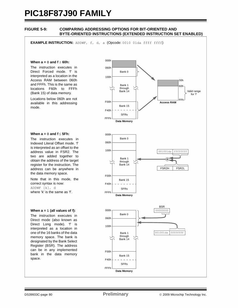
PIC18F87J90 FAMILY
DS39933C-page 80 Preliminary © 2009 Microchip Technology Inc.
FIGURE 5-9: COMPARING ADDRESSING OPTIONS FOR BIT-ORIENTED AND BYTE-ORIENTED INSTRUCTIONS (EXTENDED INSTRUCTION SET ENABLED)
EXAMPLE INSTRUCTION: ADDWF, f, d, a (Opcode: 0010 01da ffff ffff)
When a = 0 and f ≥ 60h:The instruction executes inDirect Forced mode. ‘f’ isinterpreted as a location in theAccess RAM between 060hand FFFh. This is the same aslocations F60h to FFFh(Bank 15) of data memory.
Locations below 060h are notavailable in this addressingmode.
When a = 0 and f ≤ 5Fh:The instruction executes inIndexed Literal Offset mode. ‘f’is interpreted as an offset to theaddress value in FSR2. Thetwo are added together toobtain the address of the targetregister for the instruction. Theaddress can be anywhere inthe data memory space.
Note that in this mode, thecorrect syntax is now:ADDWF [k], dwhere ‘k’ is the same as ‘f’.
When a = 1 (all values of f):The instruction executes inDirect mode (also known asDirect Long mode). ‘f’ isinterpreted as a location inone of the 16 banks of the datamemory space. The bank isdesignated by the Bank SelectRegister (BSR). The addresscan be in any implementedbank in the data memoryspace.
000h
060h
100h
F00h
F40h
FFFh
Valid range
00h
60h
FFh
Data Memory
Access RAM
Bank 0
Bank 1throughBank 14
Bank 15
SFRs
000h
060h
100h
F00h
F40h
FFFhData Memory
Bank 0
Bank 1throughBank 14
Bank 15
SFRs
FSR2H FSR2L
ffffffff001001da
ffffffff001001da
000h
060h
100h
F00h
F40h
FFFhData Memory
Bank 0
Bank 1throughBank 14
Bank 15
SFRs
for ‘f’
BSR00000000
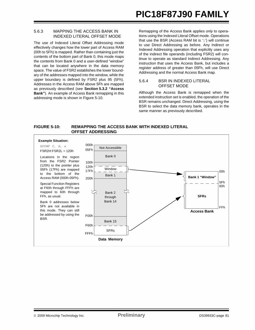
© 2009 Microchip Technology Inc. Preliminary DS39933C-page 81
PIC18F87J90 FAMILY5.6.3 MAPPING THE ACCESS BANK IN
INDEXED LITERAL OFFSET MODEThe use of Indexed Literal Offset Addressing modeeffectively changes how the lower part of Access RAM(00h to 5Fh) is mapped. Rather than containing just thecontents of the bottom part of Bank 0, this mode mapsthe contents from Bank 0 and a user-defined “window”that can be located anywhere in the data memoryspace. The value of FSR2 establishes the lower bound-ary of the addresses mapped into the window, while theupper boundary is defined by FSR2 plus 95 (5Fh).Addresses in the Access RAM above 5Fh are mappedas previously described (see Section 5.3.2 “AccessBank”). An example of Access Bank remapping in thisaddressing mode is shown in Figure 5-10.
Remapping of the Access Bank applies only to opera-tions using the Indexed Literal Offset mode. Operationsthat use the BSR (Access RAM bit is ‘1’) will continueto use Direct Addressing as before. Any Indirect orIndexed Addressing operation that explicitly uses anyof the indirect file operands (including FSR2) will con-tinue to operate as standard Indirect Addressing. Anyinstruction that uses the Access Bank, but includes aregister address of greater than 05Fh, will use DirectAddressing and the normal Access Bank map.
5.6.4 BSR IN INDEXED LITERAL OFFSET MODE
Although the Access Bank is remapped when theextended instruction set is enabled, the operation of theBSR remains unchanged. Direct Addressing, using theBSR to select the data memory bank, operates in thesame manner as previously described.
FIGURE 5-10: REMAPPING THE ACCESS BANK WITH INDEXED LITERAL OFFSET ADDRESSING
Data Memory
000h
100h
200h
F60h
F00h
FFFh
Bank 1
Bank 15
Bank 2throughBank 14
SFRs
05FhADDWF f, d, a
FSR2H:FSR2L = 120h
Locations in the regionfrom the FSR2 Pointer(120h) to the pointer plus05Fh (17Fh) are mappedto the bottom of theAccess RAM (000h-05Fh).
Special Function Registersat F60h through FFFh aremapped to 60h throughFFh, as usual.
Bank 0 addresses below5Fh are not available inthis mode. They can stillbe addressed by using theBSR.
Access Bank
00h
FFh
Bank 0
SFRs
Bank 1 “Window”
Not Accessible
Window
Example Situation:
120h17Fh
5Fh60h

PIC18F87J90 FAMILY
DS39933C-page 82 Preliminary © 2009 Microchip Technology Inc.
NOTES:
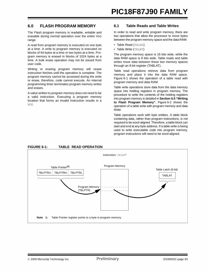
© 2009 Microchip Technology Inc. Preliminary DS39933C-page 83
PIC18F87J90 FAMILY
6.0 FLASH PROGRAM MEMORYThe Flash program memory is readable, writable anderasable during normal operation over the entire VDDrange.
A read from program memory is executed on one byteat a time. A write to program memory is executed onblocks of 64 bytes at a time or two bytes at a time. Pro-gram memory is erased in blocks of 1024 bytes at atime. A bulk erase operation may not be issued fromuser code.
Writing or erasing program memory will ceaseinstruction fetches until the operation is complete. Theprogram memory cannot be accessed during the writeor erase, therefore, code cannot execute. An internalprogramming timer terminates program memory writesand erases.
A value written to program memory does not need to bea valid instruction. Executing a program memorylocation that forms an invalid instruction results in aNOP.
6.1 Table Reads and Table WritesIn order to read and write program memory, there aretwo operations that allow the processor to move bytesbetween the program memory space and the data RAM:
• Table Read (TBLRD)• Table Write (TBLWT)
The program memory space is 16 bits wide, while thedata RAM space is 8 bits wide. Table reads and tablewrites move data between these two memory spacesthrough an 8-bit register (TABLAT).
Table read operations retrieve data from programmemory and place it into the data RAM space.Figure 6-1 shows the operation of a table read withprogram memory and data RAM.
Table write operations store data from the data memoryspace into holding registers in program memory. Theprocedure to write the contents of the holding registersinto program memory is detailed in Section 6.5 “Writingto Flash Program Memory”. Figure 6-2 shows theoperation of a table write with program memory and dataRAM.
Table operations work with byte entities. A table blockcontaining data, rather than program instructions, is notrequired to be word-aligned. Therefore, a table block canstart and end at any byte address. If a table write is beingused to write executable code into program memory,program instructions will need to be word-aligned.
FIGURE 6-1: TABLE READ OPERATION
Table Pointer(1)Table Latch (8-bit)
Program Memory
TBLPTRH TBLPTRLTABLAT
TBLPTRU
Instruction: TBLRD*
Note 1: Table Pointer register points to a byte in program memory.
Program Memory(TBLPTR)
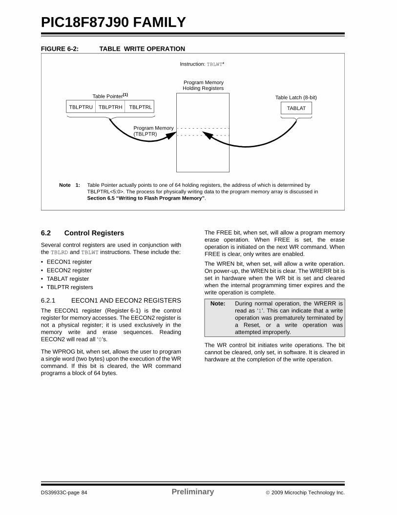
PIC18F87J90 FAMILY
DS39933C-page 84 Preliminary © 2009 Microchip Technology Inc.
FIGURE 6-2: TABLE WRITE OPERATION
6.2 Control RegistersSeveral control registers are used in conjunction withthe TBLRD and TBLWT instructions. These include the:
• EECON1 register• EECON2 register• TABLAT register• TBLPTR registers
6.2.1 EECON1 AND EECON2 REGISTERSThe EECON1 register (Register 6-1) is the controlregister for memory accesses. The EECON2 register isnot a physical register; it is used exclusively in thememory write and erase sequences. ReadingEECON2 will read all ‘0’s.
The WPROG bit, when set, allows the user to programa single word (two bytes) upon the execution of the WRcommand. If this bit is cleared, the WR commandprograms a block of 64 bytes.
The FREE bit, when set, will allow a program memoryerase operation. When FREE is set, the eraseoperation is initiated on the next WR command. WhenFREE is clear, only writes are enabled.
The WREN bit, when set, will allow a write operation.On power-up, the WREN bit is clear. The WRERR bit isset in hardware when the WR bit is set and clearedwhen the internal programming timer expires and thewrite operation is complete.
The WR control bit initiates write operations. The bitcannot be cleared, only set, in software. It is cleared inhardware at the completion of the write operation.
Table Pointer(1) Table Latch (8-bit)
TBLPTRH TBLPTRL TABLAT
Program Memory(TBLPTR)
TBLPTRU
Instruction: TBLWT*
Note 1: Table Pointer actually points to one of 64 holding registers, the address of which is determined by TBLPTRL<5:0>. The process for physically writing data to the program memory array is discussed in Section 6.5 “Writing to Flash Program Memory”.
Holding Registers Program Memory
Note: During normal operation, the WRERR isread as ‘1’. This can indicate that a writeoperation was prematurely terminated bya Reset, or a write operation wasattempted improperly.
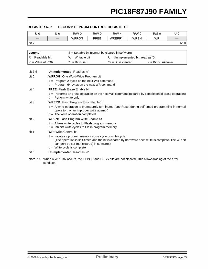
© 2009 Microchip Technology Inc. Preliminary DS39933C-page 85
PIC18F87J90 FAMILY REGISTER 6-1: EECON1: EEPROM CONTROL REGISTER 1
U-0 U-0 R/W-0 R/W-0 R/W-x R/W-0 R/S-0 U-0— — WPROG FREE WRERR(1) WREN WR —
bit 7 bit 0
Legend: S = Settable bit (cannot be cleared in software)R = Readable bit W = Writable bit U = Unimplemented bit, read as ‘0’-n = Value at POR ‘1’ = Bit is set ‘0’ = Bit is cleared x = Bit is unknown
bit 7-6 Unimplemented: Read as ‘0’bit 5 WPROG: One Word-Wide Program bit
1 = Program 2 bytes on the next WR command0 = Program 64 bytes on the next WR command
bit 4 FREE: Flash Erase Enable bit1 = Performs an erase operation on the next WR command (cleared by completion of erase operation)0 = Perform write only
bit 3 WRERR: Flash Program Error Flag bit(1)
1 = A write operation is prematurely terminated (any Reset during self-timed programming in normaloperation, or an improper write attempt)
0 = The write operation completedbit 2 WREN: Flash Program Write Enable bit
1 = Allows write cycles to Flash program memory0 = Inhibits write cycles to Flash program memory
bit 1 WR: Write Control bit1 = Initiates a program memory erase cycle or write cycle
(The operation is self-timed and the bit is cleared by hardware once write is complete. The WR bitcan only be set (not cleared) in software.)
0 = Write cycle is completebit 0 Unimplemented: Read as ‘0’
Note 1: When a WRERR occurs, the EEPGD and CFGS bits are not cleared. This allows tracing of the error condition.
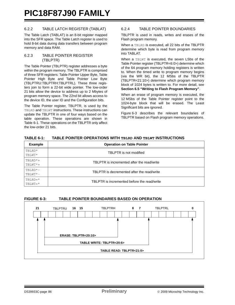
PIC18F87J90 FAMILY
DS39933C-page 86 Preliminary © 2009 Microchip Technology Inc.
6.2.2 TABLE LATCH REGISTER (TABLAT)The Table Latch (TABLAT) is an 8-bit register mappedinto the SFR space. The Table Latch register is used tohold 8-bit data during data transfers between programmemory and data RAM.
6.2.3 TABLE POINTER REGISTER (TBLPTR)
The Table Pointer (TBLPTR) register addresses a bytewithin the program memory. The TBLPTR is comprisedof three SFR registers: Table Pointer Upper Byte, TablePointer High Byte and Table Pointer Low Byte(TBLPTRU:TBLPTRH:TBLPTRL). These three regis-ters join to form a 22-bit wide pointer. The low-order21 bits allow the device to address up to 2 Mbytes ofprogram memory space. The 22nd bit allows access tothe device ID, the user ID and the Configuration bits.
The Table Pointer register, TBLPTR, is used by theTBLRD and TBLWT instructions. These instructions canupdate the TBLPTR in one of four ways based on thetable operation. These operations are shown inTable 6-1. These operations on the TBLPTR only affectthe low-order 21 bits.
6.2.4 TABLE POINTER BOUNDARIESTBLPTR is used in reads, writes and erases of theFlash program memory.
When a TBLRD is executed, all 22 bits of the TBLPTRdetermine which byte is read from program memoryinto TABLAT.
When a TBLWT is executed, the seven LSbs of theTable Pointer register (TBLPTR<6:0>) determine whichof the 64 program memory holding registers is writtento. When the timed write to program memory begins(via the WR bit), the 12 MSbs of the TBLPTR(TBLPTR<21:10>) determine which program memoryblock of 1024 bytes is written to. For more detail, seeSection 6.5 “Writing to Flash Program Memory”.
When an erase of program memory is executed, the12 MSbs of the Table Pointer register point to the1024-byte block that will be erased. The LeastSignificant bits are ignored.
Figure 6-3 describes the relevant boundaries ofTBLPTR based on Flash program memory operations.
TABLE 6-1: TABLE POINTER OPERATIONS WITH TBLRD AND TBLWT INSTRUCTIONS
FIGURE 6-3: TABLE POINTER BOUNDARIES BASED ON OPERATION
Example Operation on Table Pointer
TBLRD*TBLWT*
TBLPTR is not modified
TBLRD*+TBLWT*+
TBLPTR is incremented after the read/write
TBLRD*-TBLWT*-
TBLPTR is decremented after the read/write
TBLRD+*TBLWT+*
TBLPTR is incremented before the read/write
21 16 15 8 7 0
ERASE: TBLPTR<20:10>
TABLE WRITE: TBLPTR<20:6>
TABLE READ: TBLPTR<21:0>
TBLPTRLTBLPTRHTBLPTRU
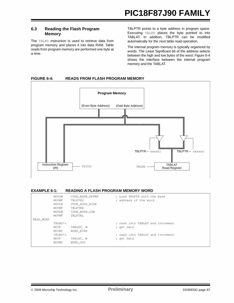
© 2009 Microchip Technology Inc. Preliminary DS39933C-page 87
PIC18F87J90 FAMILY6.3 Reading the Flash Program
MemoryThe TBLRD instruction is used to retrieve data fromprogram memory and places it into data RAM. Tablereads from program memory are performed one byte ata time.
TBLPTR points to a byte address in program space.Executing TBLRD places the byte pointed to intoTABLAT. In addition, TBLPTR can be modifiedautomatically for the next table read operation.
The internal program memory is typically organized bywords. The Least Significant bit of the address selectsbetween the high and low bytes of the word. Figure 6-4shows the interface between the internal programmemory and the TABLAT.
FIGURE 6-4: READS FROM FLASH PROGRAM MEMORY
EXAMPLE 6-1: READING A FLASH PROGRAM MEMORY WORD
(Even Byte Address)
Program Memory
(Odd Byte Address)
TBLRD TABLAT
TBLPTR = xxxxx1
FETCHInstruction Register (IR) Read Register
TBLPTR = xxxxx0
MOVLW CODE_ADDR_UPPER ; Load TBLPTR with the baseMOVWF TBLPTRU ; address of the wordMOVLW CODE_ADDR_HIGHMOVWF TBLPTRHMOVLW CODE_ADDR_LOWMOVWF TBLPTRL
READ_WORDTBLRD*+ ; read into TABLAT and incrementMOVF TABLAT, W ; get dataMOVWF WORD_EVENTBLRD*+ ; read into TABLAT and incrementMOVF TABLAT, W ; get dataMOVWF WORD_ODD
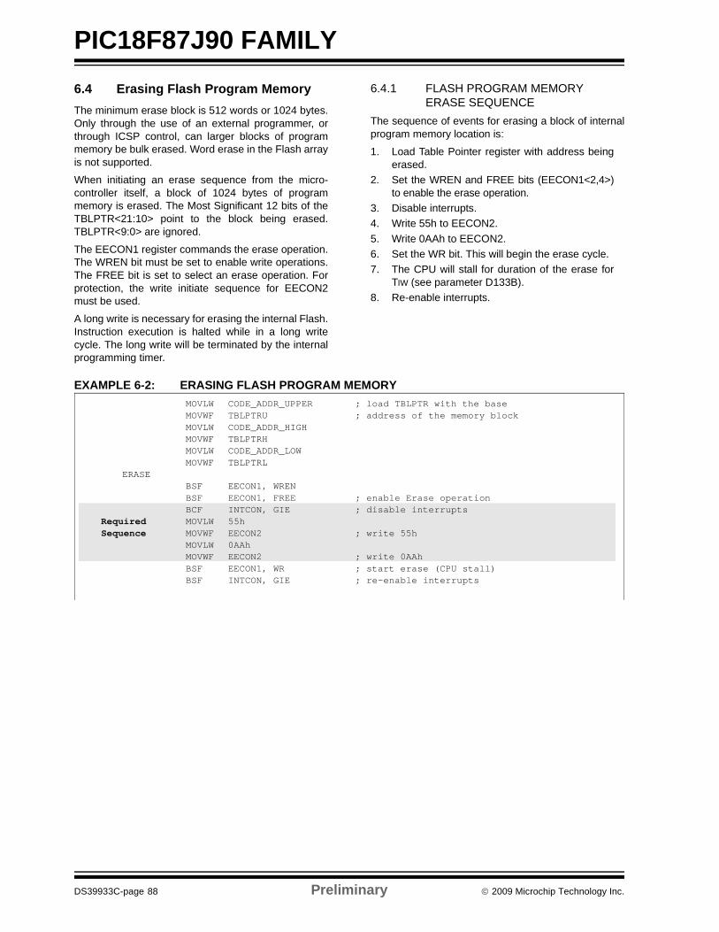
PIC18F87J90 FAMILY
DS39933C-page 88 Preliminary © 2009 Microchip Technology Inc.
6.4 Erasing Flash Program MemoryThe minimum erase block is 512 words or 1024 bytes.Only through the use of an external programmer, orthrough ICSP control, can larger blocks of programmemory be bulk erased. Word erase in the Flash arrayis not supported.
When initiating an erase sequence from the micro-controller itself, a block of 1024 bytes of programmemory is erased. The Most Significant 12 bits of theTBLPTR<21:10> point to the block being erased.TBLPTR<9:0> are ignored.
The EECON1 register commands the erase operation.The WREN bit must be set to enable write operations.The FREE bit is set to select an erase operation. Forprotection, the write initiate sequence for EECON2must be used.
A long write is necessary for erasing the internal Flash.Instruction execution is halted while in a long writecycle. The long write will be terminated by the internalprogramming timer.
6.4.1 FLASH PROGRAM MEMORY ERASE SEQUENCE
The sequence of events for erasing a block of internalprogram memory location is:
1. Load Table Pointer register with address beingerased.
2. Set the WREN and FREE bits (EECON1<2,4>)to enable the erase operation.
3. Disable interrupts.4. Write 55h to EECON2.5. Write 0AAh to EECON2.6. Set the WR bit. This will begin the erase cycle.7. The CPU will stall for duration of the erase for
TIW (see parameter D133B).8. Re-enable interrupts.
EXAMPLE 6-2: ERASING FLASH PROGRAM MEMORY MOVLW CODE_ADDR_UPPER ; load TBLPTR with the baseMOVWF TBLPTRU ; address of the memory blockMOVLW CODE_ADDR_HIGHMOVWF TBLPTRH MOVLW CODE_ADDR_LOWMOVWF TBLPTRL
ERASE BSF EECON1, WRENBSF EECON1, FREE ; enable Erase operationBCF INTCON, GIE ; disable interrupts
Required MOVLW 55hSequence MOVWF EECON2 ; write 55h
MOVLW 0AAhMOVWF EECON2 ; write 0AAhBSF EECON1, WR ; start erase (CPU stall)BSF INTCON, GIE ; re-enable interrupts
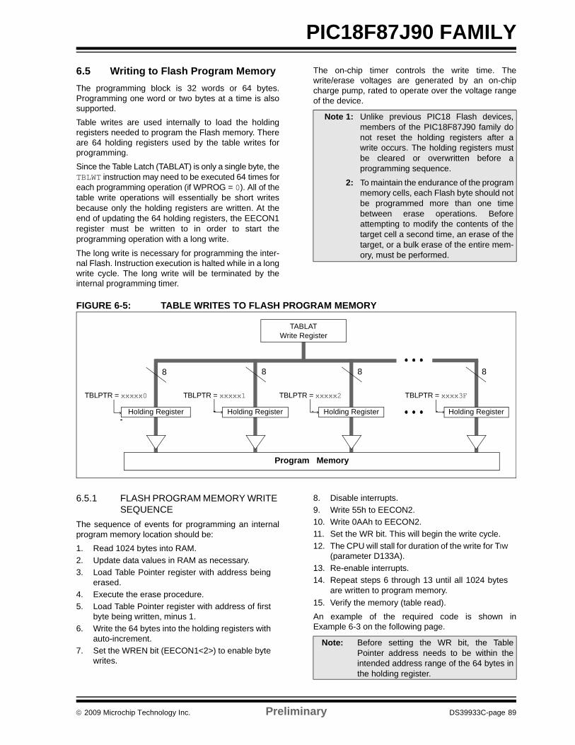
© 2009 Microchip Technology Inc. Preliminary DS39933C-page 89
PIC18F87J90 FAMILY6.5 Writing to Flash Program MemoryThe programming block is 32 words or 64 bytes.Programming one word or two bytes at a time is alsosupported.Table writes are used internally to load the holdingregisters needed to program the Flash memory. Thereare 64 holding registers used by the table writes forprogramming.Since the Table Latch (TABLAT) is only a single byte, theTBLWT instruction may need to be executed 64 times foreach programming operation (if WPROG = 0). All of thetable write operations will essentially be short writesbecause only the holding registers are written. At theend of updating the 64 holding registers, the EECON1register must be written to in order to start theprogramming operation with a long write.
The long write is necessary for programming the inter-nal Flash. Instruction execution is halted while in a longwrite cycle. The long write will be terminated by theinternal programming timer.
The on-chip timer controls the write time. Thewrite/erase voltages are generated by an on-chipcharge pump, rated to operate over the voltage rangeof the device.
FIGURE 6-5: TABLE WRITES TO FLASH PROGRAM MEMORY
6.5.1 FLASH PROGRAM MEMORY WRITE SEQUENCE
The sequence of events for programming an internalprogram memory location should be:1. Read 1024 bytes into RAM.2. Update data values in RAM as necessary.3. Load Table Pointer register with address being
erased.4. Execute the erase procedure.5. Load Table Pointer register with address of first
byte being written, minus 1.6. Write the 64 bytes into the holding registers with
auto-increment.7. Set the WREN bit (EECON1<2>) to enable byte
writes.
8. Disable interrupts.9. Write 55h to EECON2.10. Write 0AAh to EECON2.11. Set the WR bit. This will begin the write cycle.12. The CPU will stall for duration of the write for TIW
(parameter D133A).13. Re-enable interrupts.14. Repeat steps 6 through 13 until all 1024 bytes
are written to program memory.15. Verify the memory (table read).An example of the required code is shown inExample 6-3 on the following page.
Note 1: Unlike previous PIC18 Flash devices,members of the PIC18F87J90 family donot reset the holding registers after awrite occurs. The holding registers mustbe cleared or overwritten before aprogramming sequence.
2: To maintain the endurance of the programmemory cells, each Flash byte should notbe programmed more than one timebetween erase operations. Beforeattempting to modify the contents of thetarget cell a second time, an erase of thetarget, or a bulk erase of the entire mem-ory, must be performed.
TBLPTR = xxxx3FTBLPTR = xxxxx1TBLPTR = xxxxx0 TBLPTR = xxxxx2
Program Memory
Holding Register Holding Register Holding Register Holding Register
8 8 8 8
TABLATWrite Register
Note: Before setting the WR bit, the TablePointer address needs to be within theintended address range of the 64 bytes inthe holding register.
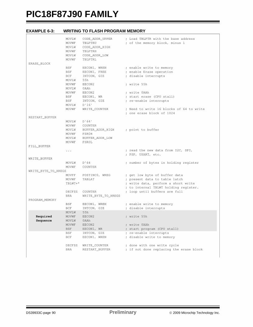
PIC18F87J90 FAMILY
DS39933C-page 90 Preliminary © 2009 Microchip Technology Inc.
EXAMPLE 6-3: WRITING TO FLASH PROGRAM MEMORY
MOVLW CODE_ADDR_UPPER ; Load TBLPTR with the base addressMOVWF TBLPTRU ; of the memory block, minus 1MOVLW CODE_ADDR_HIGHMOVWF TBLPTRHMOVLW CODE_ADDR_LOWMOVWF TBLPTRL
ERASE_BLOCKBSF EECON1, WREN ; enable write to memoryBSF EECON1, FREE ; enable Erase operationBCF INTCON, GIE ; disable interruptsMOVLW 55hMOVWF EECON2 ; write 55hMOVLW 0AAhMOVWF EECON2 ; write 0AAhBSF EECON1, WR ; start erase (CPU stall)BSF INTCON, GIE ; re-enable interruptsMOVLW D'16'MOVWF WRITE_COUNTER ; Need to write 16 blocks of 64 to write
; one erase block of 1024RESTART_BUFFER
MOVLW D'64'MOVWF COUNTERMOVLW BUFFER_ADDR_HIGH ; point to bufferMOVWF FSR0HMOVLW BUFFER_ADDR_LOWMOVWF FSR0L
FILL_BUFFER... ; read the new data from I2C, SPI,
; PSP, USART, etc. WRITE_BUFFER
MOVLW D’64 ; number of bytes in holding registerMOVWF COUNTER
WRITE_BYTE_TO_HREGSMOVFF POSTINC0, WREG ; get low byte of buffer dataMOVWF TABLAT ; present data to table latchTBLWT+* ; write data, perform a short write
; to internal TBLWT holding register.DECFSZ COUNTER ; loop until buffers are fullBRA WRITE_BYTE_TO_HREGS
PROGRAM_MEMORYBSF EECON1, WREN ; enable write to memoryBCF INTCON, GIE ; disable interruptsMOVLW 55h
Required MOVWF EECON2 ; write 55hSequence MOVLW 0AAh
MOVWF EECON2 ; write 0AAhBSF EECON1, WR ; start program (CPU stall)BSF INTCON, GIE ; re-enable interruptsBCF EECON1, WREN ; disable write to memory
DECFSZ WRITE_COUNTER ; done with one write cycleBRA RESTART_BUFFER ; if not done replacing the erase block
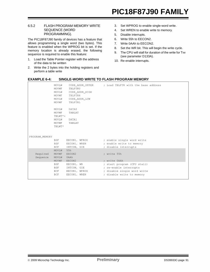
© 2009 Microchip Technology Inc. Preliminary DS39933C-page 91
PIC18F87J90 FAMILY6.5.2 FLASH PROGRAM MEMORY WRITE
SEQUENCE (WORD PROGRAMMING).
The PIC18F87J90 family of devices has a feature thatallows programming a single word (two bytes). Thisfeature is enabled when the WPROG bit is set. If thememory location is already erased, the followingsequence is required to enable this feature:1. Load the Table Pointer register with the address
of the data to be written2. Write the 2 bytes into the holding registers and
perform a table write
3. Set WPROG to enable single-word write.4. Set WREN to enable write to memory.5. Disable interrupts.6. Write 55h to EECON2.7. Write 0AAh to EECON2.8. Set the WR bit. This will begin the write cycle.9. The CPU will stall for duration of the write for TIW
(see parameter D133A).10. Re-enable interrupts.
EXAMPLE 6-4: SINGLE-WORD WRITE TO FLASH PROGRAM MEMORYMOVLW CODE_ADDR_UPPER ; Load TBLPTR with the base addressMOVWF TBLPTRUMOVLW CODE_ADDR_HIGHMOVWF TBLPTRHMOVLW CODE_ADDR_LOWMOVWF TBLPTRL
MOVLW DATA0MOVWF TABLATTBLWT*+MOVLW DATA1MOVWF TABLATTBLWT*
PROGRAM_MEMORYBSF EECON1, WPROG ; enable single word writeBSF EECON1, WREN ; enable write to memoryBCF INTCON, GIE ; disable interruptsMOVLW 55h
Required MOVWF EECON2 ; write 55hSequence MOVLW 0AAh
MOVWF EECON2 ; write 0AAhBSF EECON1, WR ; start program (CPU stall)BSF INTCON, GIE ; re-enable interruptsBCF EECON1, WPROG ; disable single word writeBCF EECON1, WREN ; disable write to memory
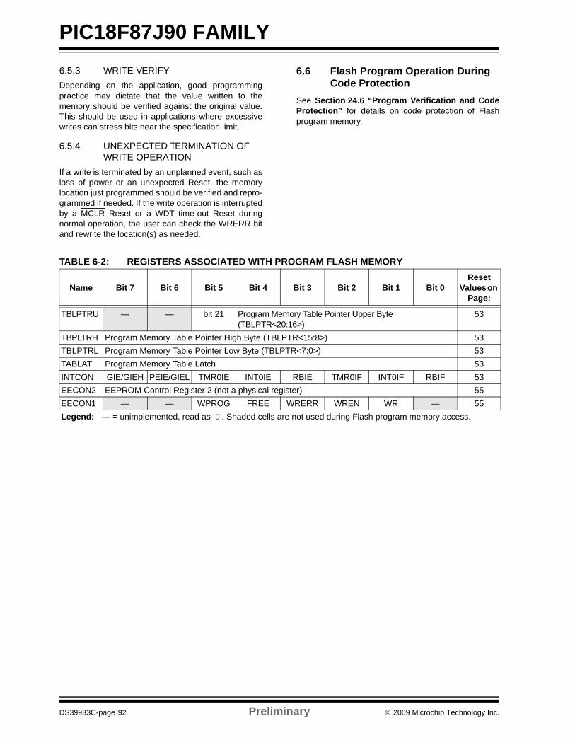
PIC18F87J90 FAMILY
DS39933C-page 92 Preliminary © 2009 Microchip Technology Inc.
6.5.3 WRITE VERIFYDepending on the application, good programmingpractice may dictate that the value written to thememory should be verified against the original value.This should be used in applications where excessivewrites can stress bits near the specification limit.
6.5.4 UNEXPECTED TERMINATION OF WRITE OPERATION
If a write is terminated by an unplanned event, such asloss of power or an unexpected Reset, the memorylocation just programmed should be verified and repro-grammed if needed. If the write operation is interruptedby a MCLR Reset or a WDT time-out Reset duringnormal operation, the user can check the WRERR bitand rewrite the location(s) as needed.
6.6 Flash Program Operation During Code Protection
See Section 24.6 “Program Verification and CodeProtection” for details on code protection of Flashprogram memory.
TABLE 6-2: REGISTERS ASSOCIATED WITH PROGRAM FLASH MEMORY
Name Bit 7 Bit 6 Bit 5 Bit 4 Bit 3 Bit 2 Bit 1 Bit 0Reset
Values on Page:
TBLPTRU — — bit 21 Program Memory Table Pointer Upper Byte (TBLPTR<20:16>)
53
TBPLTRH Program Memory Table Pointer High Byte (TBLPTR<15:8>) 53TBLPTRL Program Memory Table Pointer Low Byte (TBLPTR<7:0>) 53TABLAT Program Memory Table Latch 53INTCON GIE/GIEH PEIE/GIEL TMR0IE INT0IE RBIE TMR0IF INT0IF RBIF 53EECON2 EEPROM Control Register 2 (not a physical register) 55EECON1 — — WPROG FREE WRERR WREN WR — 55Legend: — = unimplemented, read as ‘0’. Shaded cells are not used during Flash program memory access.
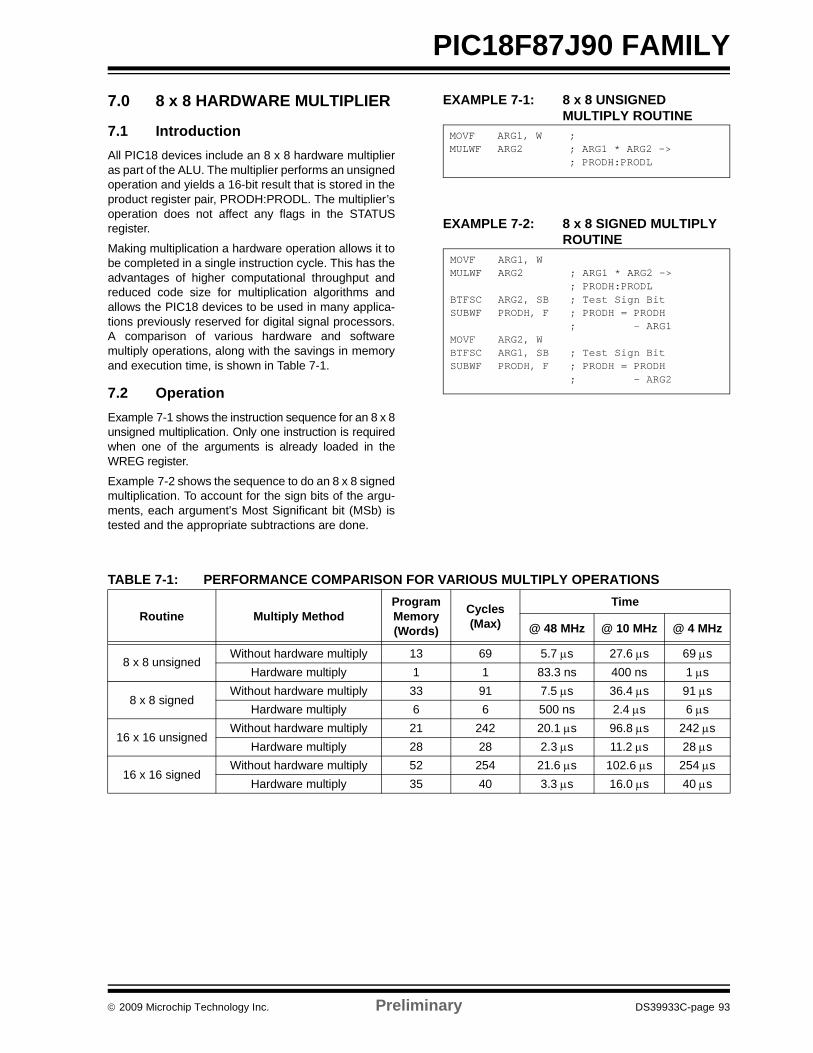
© 2009 Microchip Technology Inc. Preliminary DS39933C-page 93
PIC18F87J90 FAMILY
7.0 8 x 8 HARDWARE MULTIPLIER
7.1 IntroductionAll PIC18 devices include an 8 x 8 hardware multiplieras part of the ALU. The multiplier performs an unsignedoperation and yields a 16-bit result that is stored in theproduct register pair, PRODH:PRODL. The multiplier’soperation does not affect any flags in the STATUSregister.
Making multiplication a hardware operation allows it tobe completed in a single instruction cycle. This has theadvantages of higher computational throughput andreduced code size for multiplication algorithms andallows the PIC18 devices to be used in many applica-tions previously reserved for digital signal processors.A comparison of various hardware and softwaremultiply operations, along with the savings in memoryand execution time, is shown in Table 7-1.
7.2 OperationExample 7-1 shows the instruction sequence for an 8 x 8unsigned multiplication. Only one instruction is requiredwhen one of the arguments is already loaded in theWREG register.
Example 7-2 shows the sequence to do an 8 x 8 signedmultiplication. To account for the sign bits of the argu-ments, each argument’s Most Significant bit (MSb) istested and the appropriate subtractions are done.
EXAMPLE 7-1: 8 x 8 UNSIGNED MULTIPLY ROUTINE
EXAMPLE 7-2: 8 x 8 SIGNED MULTIPLY ROUTINE
TABLE 7-1: PERFORMANCE COMPARISON FOR VARIOUS MULTIPLY OPERATIONS
MOVF ARG1, W ; MULWF ARG2 ; ARG1 * ARG2 ->
; PRODH:PRODL
MOVF ARG1, W MULWF ARG2 ; ARG1 * ARG2 ->
; PRODH:PRODL BTFSC ARG2, SB ; Test Sign Bit SUBWF PRODH, F ; PRODH = PRODH
; - ARG1 MOVF ARG2, WBTFSC ARG1, SB ; Test Sign Bit SUBWF PRODH, F ; PRODH = PRODH
; - ARG2
Routine Multiply MethodProgramMemory(Words)
Cycles(Max)
Time
@ 48 MHz @ 10 MHz @ 4 MHz
8 x 8 unsignedWithout hardware multiply 13 69 5.7 μs 27.6 μs 69 μs
Hardware multiply 1 1 83.3 ns 400 ns 1 μs
8 x 8 signedWithout hardware multiply 33 91 7.5 μs 36.4 μs 91 μs
Hardware multiply 6 6 500 ns 2.4 μs 6 μs
16 x 16 unsignedWithout hardware multiply 21 242 20.1 μs 96.8 μs 242 μs
Hardware multiply 28 28 2.3 μs 11.2 μs 28 μs
16 x 16 signedWithout hardware multiply 52 254 21.6 μs 102.6 μs 254 μs
Hardware multiply 35 40 3.3 μs 16.0 μs 40 μs
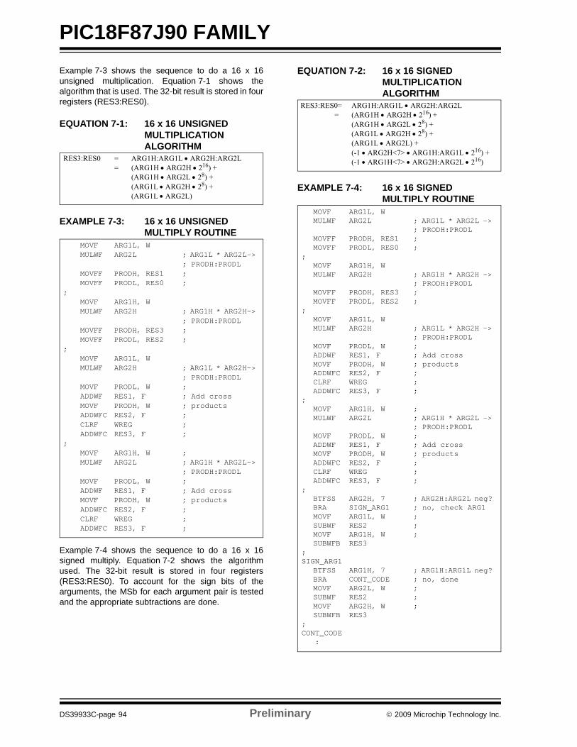
PIC18F87J90 FAMILY
DS39933C-page 94 Preliminary © 2009 Microchip Technology Inc.
Example 7-3 shows the sequence to do a 16 x 16unsigned multiplication. Equation 7-1 shows thealgorithm that is used. The 32-bit result is stored in fourregisters (RES3:RES0).
EQUATION 7-1: 16 x 16 UNSIGNED MULTIPLICATION ALGORITHM
EXAMPLE 7-3: 16 x 16 UNSIGNED MULTIPLY ROUTINE
Example 7-4 shows the sequence to do a 16 x 16signed multiply. Equation 7-2 shows the algorithmused. The 32-bit result is stored in four registers(RES3:RES0). To account for the sign bits of thearguments, the MSb for each argument pair is testedand the appropriate subtractions are done.
EQUATION 7-2: 16 x 16 SIGNED MULTIPLICATION ALGORITHM
EXAMPLE 7-4: 16 x 16 SIGNED MULTIPLY ROUTINE
RES3:RES0 = ARG1H:ARG1L • ARG2H:ARG2L= (ARG1H • ARG2H • 216) +
(ARG1H • ARG2L • 28) +(ARG1L • ARG2H • 28) +(ARG1L • ARG2L)
MOVF ARG1L, W MULWF ARG2L ; ARG1L * ARG2L->
; PRODH:PRODL MOVFF PRODH, RES1 ; MOVFF PRODL, RES0 ;
; MOVF ARG1H, W MULWF ARG2H ; ARG1H * ARG2H->
; PRODH:PRODL MOVFF PRODH, RES3 ; MOVFF PRODL, RES2 ;
; MOVF ARG1L, W MULWF ARG2H ; ARG1L * ARG2H->
; PRODH:PRODL MOVF PRODL, W ; ADDWF RES1, F ; Add cross MOVF PRODH, W ; products ADDWFC RES2, F ; CLRF WREG ; ADDWFC RES3, F ;
; MOVF ARG1H, W ; MULWF ARG2L ; ARG1H * ARG2L->
; PRODH:PRODL MOVF PRODL, W ; ADDWF RES1, F ; Add cross MOVF PRODH, W ; products ADDWFC RES2, F ; CLRF WREG ; ADDWFC RES3, F ;
RES3:RES0= ARG1H:ARG1L • ARG2H:ARG2L= (ARG1H • ARG2H • 216) +
(ARG1H • ARG2L • 28) +(ARG1L • ARG2H • 28) +(ARG1L • ARG2L) +(-1 • ARG2H<7> • ARG1H:ARG1L • 216) +(-1 • ARG1H<7> • ARG2H:ARG2L • 216)
MOVF ARG1L, W MULWF ARG2L ; ARG1L * ARG2L ->
; PRODH:PRODL MOVFF PRODH, RES1 ; MOVFF PRODL, RES0 ;
; MOVF ARG1H, W MULWF ARG2H ; ARG1H * ARG2H ->
; PRODH:PRODL MOVFF PRODH, RES3 ; MOVFF PRODL, RES2 ;
; MOVF ARG1L, W MULWF ARG2H ; ARG1L * ARG2H ->
; PRODH:PRODL MOVF PRODL, W ; ADDWF RES1, F ; Add cross MOVF PRODH, W ; products ADDWFC RES2, F ; CLRF WREG ; ADDWFC RES3, F ;
; MOVF ARG1H, W ; MULWF ARG2L ; ARG1H * ARG2L ->
; PRODH:PRODL MOVF PRODL, W ; ADDWF RES1, F ; Add cross MOVF PRODH, W ; products ADDWFC RES2, F ; CLRF WREG ; ADDWFC RES3, F ;
; BTFSS ARG2H, 7 ; ARG2H:ARG2L neg? BRA SIGN_ARG1 ; no, check ARG1 MOVF ARG1L, W ; SUBWF RES2 ; MOVF ARG1H, W ; SUBWFB RES3
; SIGN_ARG1
BTFSS ARG1H, 7 ; ARG1H:ARG1L neg? BRA CONT_CODE ; no, done MOVF ARG2L, W ; SUBWF RES2 ; MOVF ARG2H, W ; SUBWFB RES3
; CONT_CODE :
© 2009 Microchip Technology Inc. Preliminary DS39933C-page 95
PIC18F87J90 FAMILY
8.0 INTERRUPTSMembers of the PIC18F87J90 family of devices havemultiple interrupt sources and an interrupt priorityfeature that allows most interrupt sources to beassigned a high-priority level or a low-priority level. Thehigh-priority interrupt vector is at 0008h and thelow-priority interrupt vector is at 0018h. High-priorityinterrupt events will interrupt any low-priority interruptsthat may be in progress.
There are thirteen registers which are used to controlinterrupt operation. These registers are:
• RCON• INTCON• INTCON2• INTCON3• PIR1, PIR2, PIR3• PIE1, PIE2, PIE3• IPR1, IPR2, IPR3
It is recommended that the Microchip header filessupplied with MPLAB® IDE be used for the symbolic bitnames in these registers. This allows theassembler/compiler to automatically take care of theplacement of these bits within the specified register.
In general, interrupt sources have three bits to controltheir operation. They are:
• Flag bit to indicate that an interrupt event occurred
• Enable bit that allows program execution to branch to the interrupt vector address when the flag bit is set
• Priority bit to select high priority or low priority
The interrupt priority feature is enabled by setting theIPEN bit (RCON<7>). When interrupt priority isenabled, there are two bits which enable interruptsglobally. Setting the GIEH bit (INTCON<7>) enables allinterrupts that have the priority bit set (high priority).Setting the GIEL bit (INTCON<6>) enables allinterrupts that have the priority bit cleared (low priority).When the interrupt flag, enable bit and appropriateglobal interrupt enable bit are set, the interrupt willvector immediately to address 0008h or 0018h,depending on the priority bit setting. Individualinterrupts can be disabled through their correspondingenable bits.
When the IPEN bit is cleared (default state), theinterrupt priority feature is disabled and interrupts arecompatible with PIC® mid-range devices. InCompatibility mode, the interrupt priority bits for eachsource have no effect. INTCON<6> is the PEIE bitwhich enables/disables all peripheral interrupt sources.INTCON<7> is the GIE bit which enables/disables allinterrupt sources. All interrupts branch to address0008h in Compatibility mode.
When an interrupt is responded to, the global interruptenable bit is cleared to disable further interrupts. If theIPEN bit is cleared, this is the GIE bit. If interrupt prioritylevels are used, this will be either the GIEH or GIEL bit.High-priority interrupt sources can interrupt alow-priority interrupt. Low-priority interrupts are notprocessed while high-priority interrupts are in progress.
The return address is pushed onto the stack and thePC is loaded with the interrupt vector address (0008hor 0018h). Once in the Interrupt Service Routine, thesource(s) of the interrupt can be determined by pollingthe interrupt flag bits. The interrupt flag bits must becleared in software before re-enabling interrupts toavoid recursive interrupts.
The “return from interrupt” instruction, RETFIE, exitsthe interrupt routine and sets the GIE bit (GIEH or GIELif priority levels are used) which re-enables interrupts.
For external interrupt events, such as the INTx pins orthe PORTB input change interrupt, the interrupt latencywill be three to four instruction cycles. The exactlatency is the same for one or two-cycle instructions.Individual interrupt flag bits are set regardless of thestatus of their corresponding enable bit or the GIE bit.
Note: Do not use the MOVFF instruction to modifyany of the Interrupt Control registers whileany interrupt is enabled. Doing so maycause erratic microcontroller behavior.
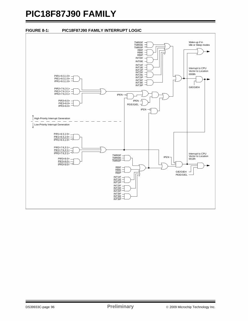
PIC18F87J90 FAMILY
DS39933C-page 96 Preliminary © 2009 Microchip Technology Inc.
FIGURE 8-1: PIC18F87J90 FAMILY INTERRUPT LOGIC
TMR0IE
GIE/GIEH
PEIE/GIEL
Wake-up if in
Interrupt to CPUVector to Location0008h
INT2IFINT2IEINT2IP
INT1IFINT1IEINT1IP
TMR0IFTMR0IETMR0IP
RBIFRBIERBIP
IPEN
TMR0IF
TMR0IP
INT1IFINT1IEINT1IPINT2IFINT2IEINT2IP
RBIFRBIERBIP
INT0IFINT0IE
PEIE/GIEL
Interrupt to CPUVector to Location
IPEN
IPEN
0018h
PIR1<6:3,1:0>PIE1<6:3,1:0>IPR1<6:3,1:0>
High-Priority Interrupt Generation
Low-Priority Interrupt Generation
Idle or Sleep modes
GIE/GIEH
INT3IFINT3IEINT3IP
INT3IFINT3IEINT3IP
PIR2<7:6,3:1>PIE2<7:6 3:1>IPR2<7:6,3:1>
PIR3<6:0>PIE3<6:0>IPR3<6:0>
PIR1<6:3,1:0>PIE1<6:3,1:0>IPR1<6:3,1:0>
PIR2<7:6,3:1>PIE2<7:6,3:1>IPR2<7:6,3:1>
PIR3<6:0>PIE3<6:0> IPR3<6:0>
IPEN
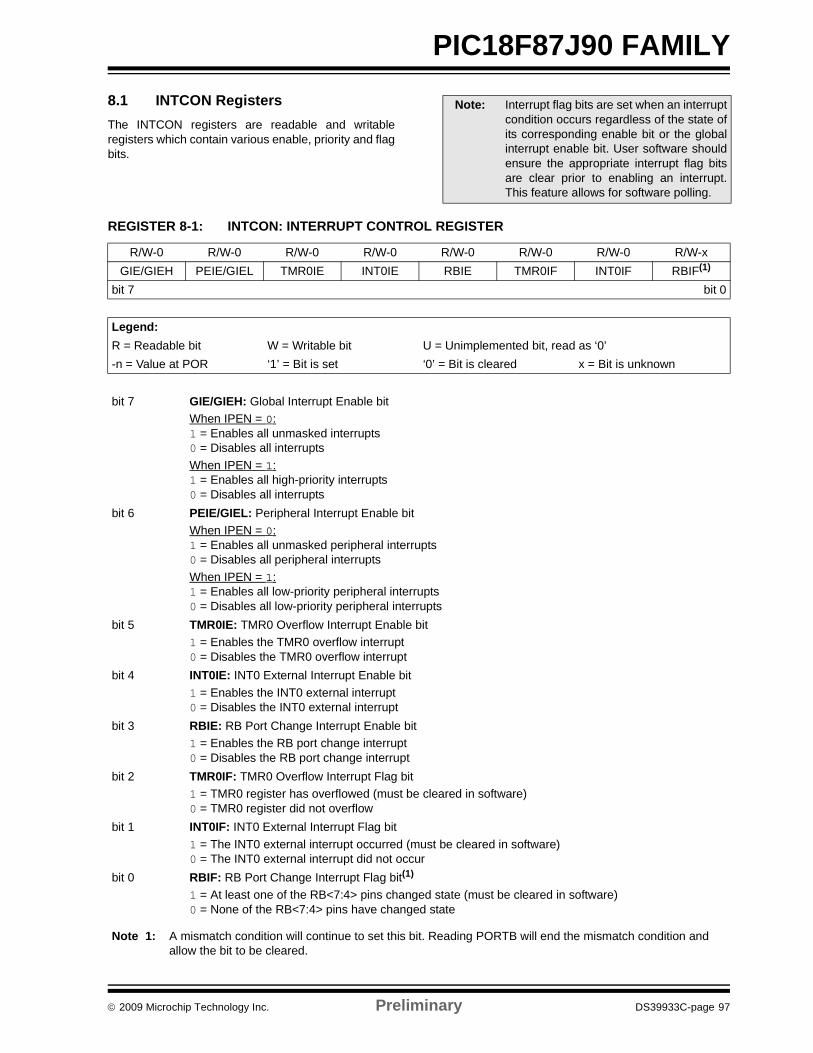
© 2009 Microchip Technology Inc. Preliminary DS39933C-page 97
PIC18F87J90 FAMILY8.1 INTCON RegistersThe INTCON registers are readable and writableregisters which contain various enable, priority and flagbits.
Note: Interrupt flag bits are set when an interruptcondition occurs regardless of the state ofits corresponding enable bit or the globalinterrupt enable bit. User software shouldensure the appropriate interrupt flag bitsare clear prior to enabling an interrupt.This feature allows for software polling.
REGISTER 8-1: INTCON: INTERRUPT CONTROL REGISTER
R/W-0 R/W-0 R/W-0 R/W-0 R/W-0 R/W-0 R/W-0 R/W-xGIE/GIEH PEIE/GIEL TMR0IE INT0IE RBIE TMR0IF INT0IF RBIF(1)
bit 7 bit 0
Legend:R = Readable bit W = Writable bit U = Unimplemented bit, read as ‘0’-n = Value at POR ‘1’ = Bit is set ‘0’ = Bit is cleared x = Bit is unknown
bit 7 GIE/GIEH: Global Interrupt Enable bitWhen IPEN = 0:1 = Enables all unmasked interrupts0 = Disables all interrupts When IPEN = 1:1 = Enables all high-priority interrupts 0 = Disables all interrupts
bit 6 PEIE/GIEL: Peripheral Interrupt Enable bitWhen IPEN = 0:1 = Enables all unmasked peripheral interrupts 0 = Disables all peripheral interrupts When IPEN = 1:1 = Enables all low-priority peripheral interrupts 0 = Disables all low-priority peripheral interrupts
bit 5 TMR0IE: TMR0 Overflow Interrupt Enable bit 1 = Enables the TMR0 overflow interrupt 0 = Disables the TMR0 overflow interrupt
bit 4 INT0IE: INT0 External Interrupt Enable bit 1 = Enables the INT0 external interrupt 0 = Disables the INT0 external interrupt
bit 3 RBIE: RB Port Change Interrupt Enable bit 1 = Enables the RB port change interrupt 0 = Disables the RB port change interrupt
bit 2 TMR0IF: TMR0 Overflow Interrupt Flag bit 1 = TMR0 register has overflowed (must be cleared in software) 0 = TMR0 register did not overflow
bit 1 INT0IF: INT0 External Interrupt Flag bit 1 = The INT0 external interrupt occurred (must be cleared in software) 0 = The INT0 external interrupt did not occur
bit 0 RBIF: RB Port Change Interrupt Flag bit(1)
1 = At least one of the RB<7:4> pins changed state (must be cleared in software) 0 = None of the RB<7:4> pins have changed state
Note 1: A mismatch condition will continue to set this bit. Reading PORTB will end the mismatch condition and allow the bit to be cleared.
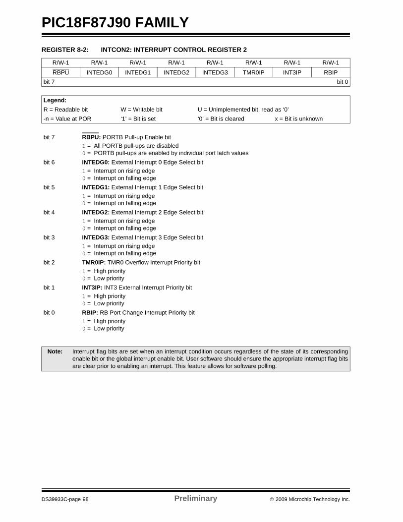
PIC18F87J90 FAMILY
DS39933C-page 98 Preliminary © 2009 Microchip Technology Inc.
REGISTER 8-2: INTCON2: INTERRUPT CONTROL REGISTER 2
R/W-1 R/W-1 R/W-1 R/W-1 R/W-1 R/W-1 R/W-1 R/W-1
RBPU INTEDG0 INTEDG1 INTEDG2 INTEDG3 TMR0IP INT3IP RBIPbit 7 bit 0
Legend:R = Readable bit W = Writable bit U = Unimplemented bit, read as ‘0’-n = Value at POR ‘1’ = Bit is set ‘0’ = Bit is cleared x = Bit is unknown
bit 7 RBPU: PORTB Pull-up Enable bit 1 = All PORTB pull-ups are disabled 0 = PORTB pull-ups are enabled by individual port latch values
bit 6 INTEDG0: External Interrupt 0 Edge Select bit 1 = Interrupt on rising edge 0 = Interrupt on falling edge
bit 5 INTEDG1: External Interrupt 1 Edge Select bit 1 = Interrupt on rising edge 0 = Interrupt on falling edge
bit 4 INTEDG2: External Interrupt 2 Edge Select bit 1 = Interrupt on rising edge 0 = Interrupt on falling edge
bit 3 INTEDG3: External Interrupt 3 Edge Select bit 1 = Interrupt on rising edge 0 = Interrupt on falling edge
bit 2 TMR0IP: TMR0 Overflow Interrupt Priority bit 1 = High priority 0 = Low priority
bit 1 INT3IP: INT3 External Interrupt Priority bit1 = High priority 0 = Low priority
bit 0 RBIP: RB Port Change Interrupt Priority bit1 = High priority 0 = Low priority
Note: Interrupt flag bits are set when an interrupt condition occurs regardless of the state of its correspondingenable bit or the global interrupt enable bit. User software should ensure the appropriate interrupt flag bitsare clear prior to enabling an interrupt. This feature allows for software polling.
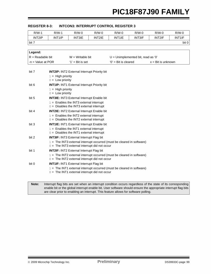
© 2009 Microchip Technology Inc. Preliminary DS39933C-page 99
PIC18F87J90 FAMILY
REGISTER 8-3: INTCON3: INTERRUPT CONTROL REGISTER 3
R/W-1 R/W-1 R/W-0 R/W-0 R/W-0 R/W-0 R/W-0 R/W-0INT2IP INT1IP INT3IE INT2IE INT1IE INT3IF INT2IF INT1IF
bit 7 bit 0
Legend:R = Readable bit W = Writable bit U = Unimplemented bit, read as ‘0’-n = Value at POR ‘1’ = Bit is set ‘0’ = Bit is cleared x = Bit is unknown
bit 7 INT2IP: INT2 External Interrupt Priority bit1 = High priority 0 = Low priority
bit 6 INT1IP: INT1 External Interrupt Priority bit1 = High priority 0 = Low priority
bit 5 INT3IE: INT3 External Interrupt Enable bit1 = Enables the INT3 external interrupt 0 = Disables the INT3 external interrupt
bit 4 INT2IE: INT2 External Interrupt Enable bit1 = Enables the INT2 external interrupt 0 = Disables the INT2 external interrupt
bit 3 INT1IE: INT1 External Interrupt Enable bit 1 = Enables the INT1 external interrupt 0 = Disables the INT1 external interrupt
bit 2 INT3IF: INT3 External Interrupt Flag bit1 = The INT3 external interrupt occurred (must be cleared in software) 0 = The INT3 external interrupt did not occur
bit 1 INT2IF: INT2 External Interrupt Flag bit1 = The INT2 external interrupt occurred (must be cleared in software) 0 = The INT2 external interrupt did not occur
bit 0 INT1IF: INT1 External Interrupt Flag bit 1 = The INT1 external interrupt occurred (must be cleared in software) 0 = The INT1 external interrupt did not occur
Note: Interrupt flag bits are set when an interrupt condition occurs regardless of the state of its correspondingenable bit or the global interrupt enable bit. User software should ensure the appropriate interrupt flag bitsare clear prior to enabling an interrupt. This feature allows for software polling.
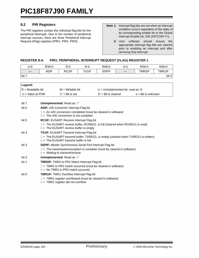
PIC18F87J90 FAMILY
DS39933C-page 100 Preliminary © 2009 Microchip Technology Inc.
8.2 PIR RegistersThe PIR registers contain the individual flag bits for theperipheral interrupts. Due to the number of peripheralinterrupt sources, there are three Peripheral InterruptRequest (Flag) registers (PIR1, PIR2, PIR3).
Note 1: Interrupt flag bits are set when an interruptcondition occurs regardless of the state ofits corresponding enable bit or the GlobalInterrupt Enable bit, GIE (INTCON<7>).
2: User software should ensure theappropriate interrupt flag bits are clearedprior to enabling an interrupt and afterservicing that interrupt.
REGISTER 8-4: PIR1: PERIPHERAL INTERRUPT REQUEST (FLAG) REGISTER 1
U-0 R/W-0 R-0 R-0 R/W-0 U-0 R/W-0 R/W-0— ADIF RC1IF TX1IF SSPIF — TMR2IF TMR1IF
bit 7 bit 0
Legend:R = Readable bit W = Writable bit U = Unimplemented bit, read as ‘0’-n = Value at POR ‘1’ = Bit is set ‘0’ = Bit is cleared x = Bit is unknown
bit 7 Unimplemented: Read as ‘0’ bit 6 ADIF: A/D Converter Interrupt Flag bit
1 = An A/D conversion completed (must be cleared in software) 0 = The A/D conversion is not complete
bit 5 RC1IF: EUSART Receive Interrupt Flag bit 1 = The EUSART receive buffer, RCREG1, is full (cleared when RCREG1 is read) 0 = The EUSART receive buffer is empty
bit 4 TX1IF: EUSART Transmit Interrupt Flag bit 1 = The EUSART transmit buffer, TXREG1, is empty (cleared when TXREG1 is written) 0 = The EUSART transmit buffer is full
bit 3 SSPIF: Master Synchronous Serial Port Interrupt Flag bit 1 = The transmission/reception is complete (must be cleared in software)0 = Waiting to transmit/receive
bit 2 Unimplemented: Read as ‘0’ bit 1 TMR2IF: TMR2 to PR2 Match Interrupt Flag bit
1 = TMR2 to PR2 match occurred (must be cleared in software) 0 = No TMR2 to PR2 match occurred
bit 0 TMR1IF: TMR1 Overflow Interrupt Flag bit 1 = TMR1 register overflowed (must be cleared in software)0 = TMR1 register did not overflow
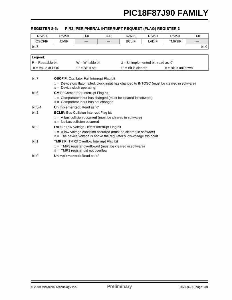
© 2009 Microchip Technology Inc. Preliminary DS39933C-page 101
PIC18F87J90 FAMILY REGISTER 8-5: PIR2: PERIPHERAL INTERRUPT REQUEST (FLAG) REGISTER 2
R/W-0 R/W-0 U-0 U-0 R/W-0 R/W-0 R/W-0 U-0OSCFIF CMIF — — BCLIF LVDIF TMR3IF —
bit 7 bit 0
Legend:R = Readable bit W = Writable bit U = Unimplemented bit, read as ‘0’-n = Value at POR ‘1’ = Bit is set ‘0’ = Bit is cleared x = Bit is unknown
bit 7 OSCFIF: Oscillator Fail Interrupt Flag bit1 = Device oscillator failed, clock input has changed to INTOSC (must be cleared in software)0 = Device clock operating
bit 6 CMIF: Comparator Interrupt Flag bit1 = Comparator input has changed (must be cleared in software)0 = Comparator input has not changed
bit 5-4 Unimplemented: Read as ‘0’ bit 3 BCLIF: Bus Collision Interrupt Flag bit
1 = A bus collision occurred (must be cleared in software)0 = No bus collision occurred
bit 2 LVDIF: Low-Voltage Detect Interrupt Flag bit 1 = A low-voltage condition occurred (must be cleared in software)0 = The device voltage is above the regulator’s low-voltage trip point
bit 1 TMR3IF: TMR3 Overflow Interrupt Flag bit1 = TMR3 register overflowed (must be cleared in software)0 = TMR3 register did not overflow
bit 0 Unimplemented: Read as ‘0’
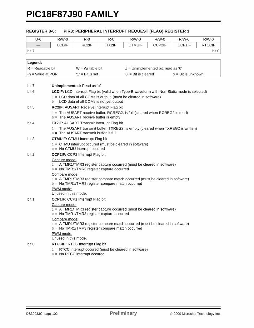
PIC18F87J90 FAMILY
DS39933C-page 102 Preliminary © 2009 Microchip Technology Inc.
REGISTER 8-6: PIR3: PERIPHERAL INTERRUPT REQUEST (FLAG) REGISTER 3
U-0 R/W-0 R-0 R-0 R/W-0 R/W-0 R/W-0 R/W-0— LCDIF RC2IF TX2IF CTMUIF CCP2IF CCP1IF RTCCIF
bit 7 bit 0
Legend:R = Readable bit W = Writable bit U = Unimplemented bit, read as ‘0’-n = Value at POR ‘1’ = Bit is set ‘0’ = Bit is cleared x = Bit is unknown
bit 7 Unimplemented: Read as ‘0’ bit 6 LCDIF: LCD Interrupt Flag bit (valid when Type-B waveform with Non-Static mode is selected)
1 = LCD data of all COMs is output (must be cleared in software)0 = LCD data of all COMs is not yet output
bit 5 RC2IF: AUSART Receive Interrupt Flag bit 1 = The AUSART receive buffer, RCREG2, is full (cleared when RCREG2 is read) 0 = The AUSART receive buffer is empty
bit 4 TX2IF: AUSART Transmit Interrupt Flag bit 1 = The AUSART transmit buffer, TXREG2, is empty (cleared when TXREG2 is written) 0 = The AUSART transmit buffer is full
bit 3 CTMUIF: CTMU Interrupt Flag bit 1 = CTMU interrupt occured (must be cleared in software)0 = No CTMU interrupt occured
bit 2 CCP2IF: CCP2 Interrupt Flag bit Capture mode: 1 = A TMR1/TMR3 register capture occurred (must be cleared in software) 0 = No TMR1/TMR3 register capture occurred Compare mode: 1 = A TMR1/TMR3 register compare match occurred (must be cleared in software) 0 = No TMR1/TMR3 register compare match occurredPWM mode:Unused in this mode.
bit 1 CCP1IF: CCP1 Interrupt Flag bit Capture mode: 1 = A TMR1/TMR3 register capture occurred (must be cleared in software) 0 = No TMR1/TMR3 register capture occurred Compare mode: 1 = A TMR1/TMR3 register compare match occurred (must be cleared in software) 0 = No TMR1/TMR3 register compare match occurredPWM mode: Unused in this mode.
bit 0 RTCCIF: RTCC Interrupt Flag bit 1 = RTCC interrupt occured (must be cleared in software)0 = No RTCC interrupt occured
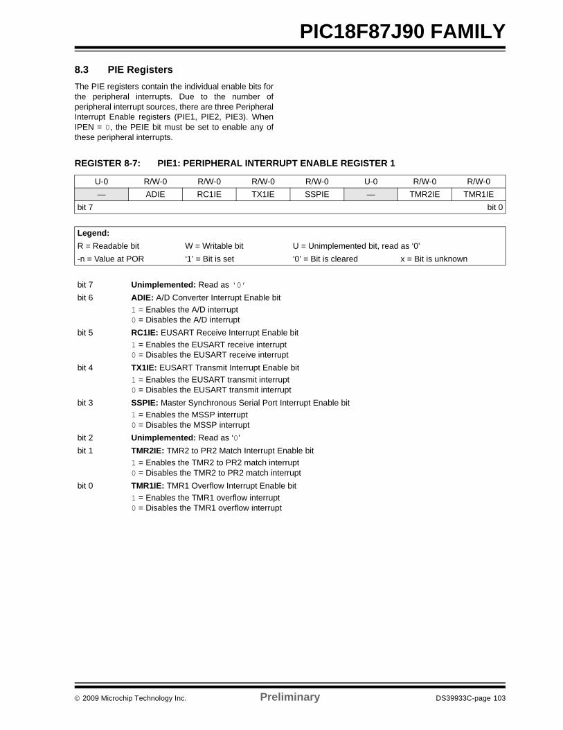
© 2009 Microchip Technology Inc. Preliminary DS39933C-page 103
PIC18F87J90 FAMILY8.3 PIE RegistersThe PIE registers contain the individual enable bits forthe peripheral interrupts. Due to the number ofperipheral interrupt sources, there are three PeripheralInterrupt Enable registers (PIE1, PIE2, PIE3). WhenIPEN = 0, the PEIE bit must be set to enable any ofthese peripheral interrupts.
REGISTER 8-7: PIE1: PERIPHERAL INTERRUPT ENABLE REGISTER 1
U-0 R/W-0 R/W-0 R/W-0 R/W-0 U-0 R/W-0 R/W-0— ADIE RC1IE TX1IE SSPIE — TMR2IE TMR1IE
bit 7 bit 0
Legend:R = Readable bit W = Writable bit U = Unimplemented bit, read as ‘0’-n = Value at POR ‘1’ = Bit is set ‘0’ = Bit is cleared x = Bit is unknown
bit 7 Unimplemented: Read as ‘0’ bit 6 ADIE: A/D Converter Interrupt Enable bit
1 = Enables the A/D interrupt 0 = Disables the A/D interrupt
bit 5 RC1IE: EUSART Receive Interrupt Enable bit1 = Enables the EUSART receive interrupt 0 = Disables the EUSART receive interrupt
bit 4 TX1IE: EUSART Transmit Interrupt Enable bit 1 = Enables the EUSART transmit interrupt 0 = Disables the EUSART transmit interrupt
bit 3 SSPIE: Master Synchronous Serial Port Interrupt Enable bit1 = Enables the MSSP interrupt 0 = Disables the MSSP interrupt
bit 2 Unimplemented: Read as ‘0’ bit 1 TMR2IE: TMR2 to PR2 Match Interrupt Enable bit
1 = Enables the TMR2 to PR2 match interrupt 0 = Disables the TMR2 to PR2 match interrupt
bit 0 TMR1IE: TMR1 Overflow Interrupt Enable bit1 = Enables the TMR1 overflow interrupt 0 = Disables the TMR1 overflow interrupt
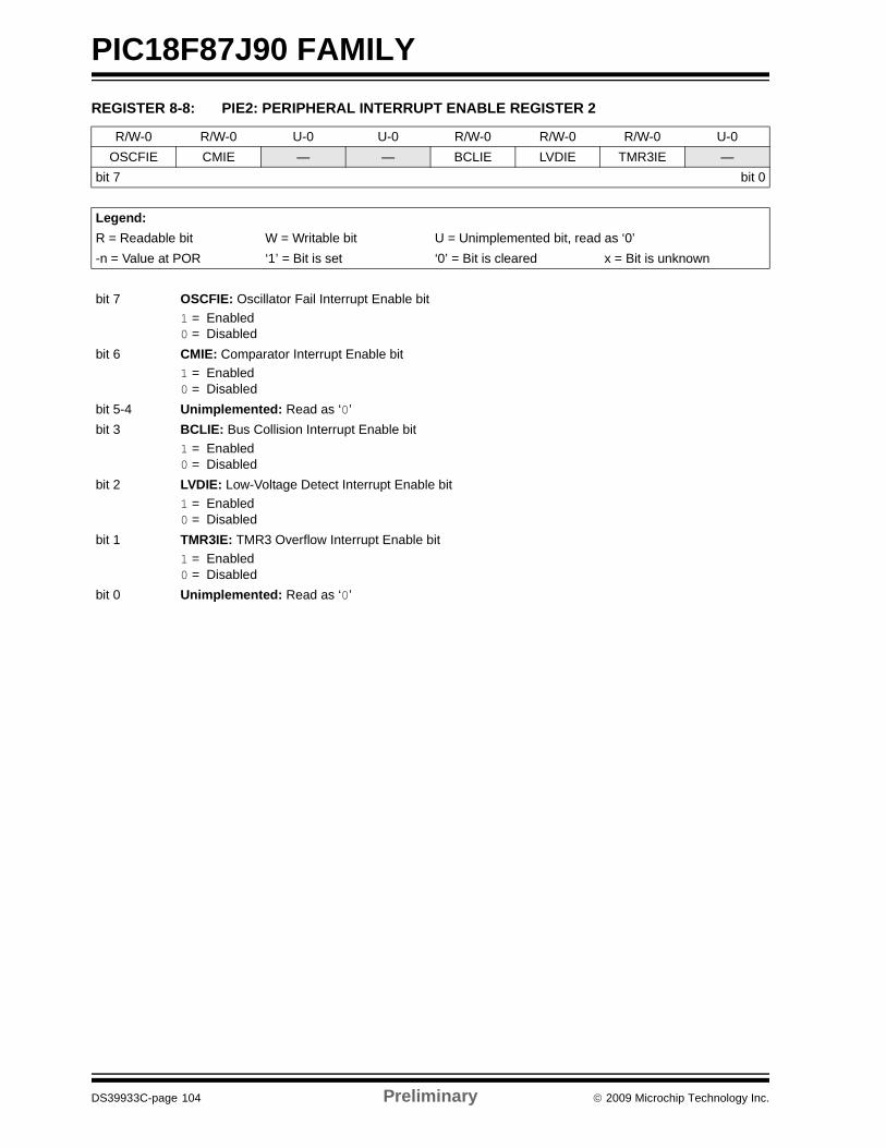
PIC18F87J90 FAMILY
DS39933C-page 104 Preliminary © 2009 Microchip Technology Inc.
REGISTER 8-8: PIE2: PERIPHERAL INTERRUPT ENABLE REGISTER 2
R/W-0 R/W-0 U-0 U-0 R/W-0 R/W-0 R/W-0 U-0OSCFIE CMIE — — BCLIE LVDIE TMR3IE —
bit 7 bit 0
Legend:R = Readable bit W = Writable bit U = Unimplemented bit, read as ‘0’-n = Value at POR ‘1’ = Bit is set ‘0’ = Bit is cleared x = Bit is unknown
bit 7 OSCFIE: Oscillator Fail Interrupt Enable bit1 = Enabled0 = Disabled
bit 6 CMIE: Comparator Interrupt Enable bit1 = Enabled0 = Disabled
bit 5-4 Unimplemented: Read as ‘0’ bit 3 BCLIE: Bus Collision Interrupt Enable bit
1 = Enabled0 = Disabled
bit 2 LVDIE: Low-Voltage Detect Interrupt Enable bit 1 = Enabled0 = Disabled
bit 1 TMR3IE: TMR3 Overflow Interrupt Enable bit 1 = Enabled0 = Disabled
bit 0 Unimplemented: Read as ‘0’
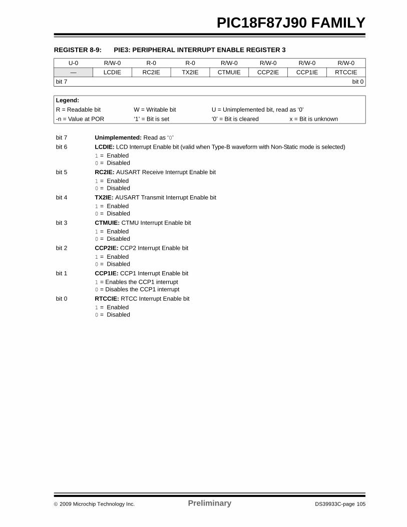
© 2009 Microchip Technology Inc. Preliminary DS39933C-page 105
PIC18F87J90 FAMILY REGISTER 8-9: PIE3: PERIPHERAL INTERRUPT ENABLE REGISTER 3
U-0 R/W-0 R-0 R-0 R/W-0 R/W-0 R/W-0 R/W-0— LCDIE RC2IE TX2IE CTMUIE CCP2IE CCP1IE RTCCIE
bit 7 bit 0
Legend:R = Readable bit W = Writable bit U = Unimplemented bit, read as ‘0’-n = Value at POR ‘1’ = Bit is set ‘0’ = Bit is cleared x = Bit is unknown
bit 7 Unimplemented: Read as ‘0’ bit 6 LCDIE: LCD Interrupt Enable bit (valid when Type-B waveform with Non-Static mode is selected)
1 = Enabled0 = Disabled
bit 5 RC2IE: AUSART Receive Interrupt Enable bit 1 = Enabled0 = Disabled
bit 4 TX2IE: AUSART Transmit Interrupt Enable bit 1 = Enabled0 = Disabled
bit 3 CTMUIE: CTMU Interrupt Enable bit1 = Enabled0 = Disabled
bit 2 CCP2IE: CCP2 Interrupt Enable bit 1 = Enabled0 = Disabled
bit 1 CCP1IE: CCP1 Interrupt Enable bit 1 = Enables the CCP1 interrupt 0 = Disables the CCP1 interrupt
bit 0 RTCCIE: RTCC Interrupt Enable bit 1 = Enabled0 = Disabled
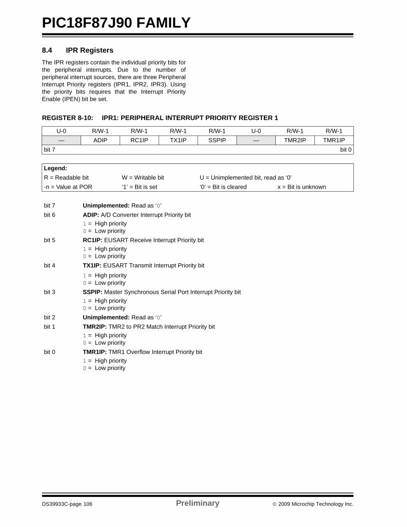
PIC18F87J90 FAMILY
DS39933C-page 106 Preliminary © 2009 Microchip Technology Inc.
8.4 IPR RegistersThe IPR registers contain the individual priority bits forthe peripheral interrupts. Due to the number ofperipheral interrupt sources, there are three PeripheralInterrupt Priority registers (IPR1, IPR2, IPR3). Usingthe priority bits requires that the Interrupt PriorityEnable (IPEN) bit be set.
REGISTER 8-10: IPR1: PERIPHERAL INTERRUPT PRIORITY REGISTER 1
U-0 R/W-1 R/W-1 R/W-1 R/W-1 U-0 R/W-1 R/W-1— ADIP RC1IP TX1IP SSPIP — TMR2IP TMR1IP
bit 7 bit 0
Legend:R = Readable bit W = Writable bit U = Unimplemented bit, read as ‘0’-n = Value at POR ‘1’ = Bit is set ‘0’ = Bit is cleared x = Bit is unknown
bit 7 Unimplemented: Read as ‘0’ bit 6 ADIP: A/D Converter Interrupt Priority bit
1 = High priority 0 = Low priority
bit 5 RC1IP: EUSART Receive Interrupt Priority bit 1 = High priority 0 = Low priority
bit 4 TX1IP: EUSART Transmit Interrupt Priority bit
1 = High priority 0 = Low priority
bit 3 SSPIP: Master Synchronous Serial Port Interrupt Priority bit 1 = High priority 0 = Low priority
bit 2 Unimplemented: Read as ‘0’ bit 1 TMR2IP: TMR2 to PR2 Match Interrupt Priority bit
1 = High priority 0 = Low priority
bit 0 TMR1IP: TMR1 Overflow Interrupt Priority bit 1 = High priority 0 = Low priority
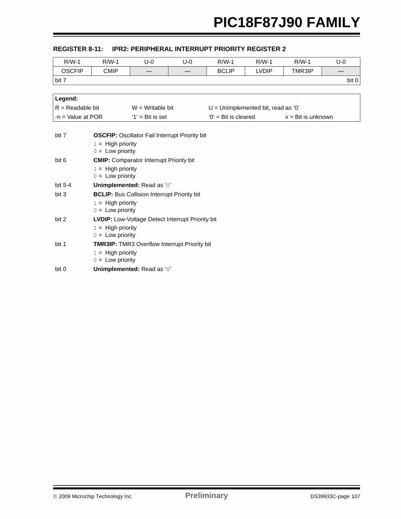
© 2009 Microchip Technology Inc. Preliminary DS39933C-page 107
PIC18F87J90 FAMILY REGISTER 8-11: IPR2: PERIPHERAL INTERRUPT PRIORITY REGISTER 2
R/W-1 R/W-1 U-0 U-0 R/W-1 R/W-1 R/W-1 U-0OSCFIP CMIP — — BCLIP LVDIP TMR3IP —
bit 7 bit 0
Legend:R = Readable bit W = Writable bit U = Unimplemented bit, read as ‘0’-n = Value at POR ‘1’ = Bit is set ‘0’ = Bit is cleared x = Bit is unknown
bit 7 OSCFIP: Oscillator Fail Interrupt Priority bit1 = High priority0 = Low priority
bit 6 CMIP: Comparator Interrupt Priority bit1 = High priority0 = Low priority
bit 5-4 Unimplemented: Read as ‘0’ bit 3 BCLIP: Bus Collision Interrupt Priority bit
1 = High priority0 = Low priority
bit 2 LVDIP: Low-Voltage Detect Interrupt Priority bit 1 = High priority0 = Low priority
bit 1 TMR3IP: TMR3 Overflow Interrupt Priority bit 1 = High priority0 = Low priority
bit 0 Unimplemented: Read as ‘0’
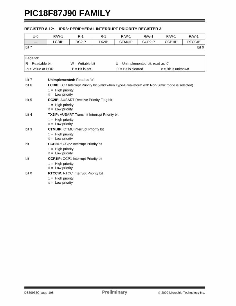
PIC18F87J90 FAMILY
DS39933C-page 108 Preliminary © 2009 Microchip Technology Inc.
REGISTER 8-12: IPR3: PERIPHERAL INTERRUPT PRIORITY REGISTER 3
U-0 R/W-1 R-1 R-1 R/W-1 R/W-1 R/W-1 R/W-1— LCDIP RC2IP TX2IP CTMUIP CCP2IP CCP1IP RTCCIP
bit 7 bit 0
Legend:R = Readable bit W = Writable bit U = Unimplemented bit, read as ‘0’-n = Value at POR ‘1’ = Bit is set ‘0’ = Bit is cleared x = Bit is unknown
bit 7 Unimplemented: Read as ‘0’ bit 6 LCDIP: LCD Interrupt Priority bit (valid when Type-B waveform with Non-Static mode is selected)
1 = High priority0 = Low priority
bit 5 RC2IP: AUSART Receive Priority Flag bit 1 = High priority0 = Low priority
bit 4 TX2IP: AUSART Transmit Interrupt Priority bit 1 = High priority0 = Low priority
bit 3 CTMUIP: CTMU Interrupt Priority bit 1 = High priority0 = Low priority
bit CCP2IP: CCP2 Interrupt Priority bit1 = High priority0 = Low priority
bit CCP1IP: CCP1 Interrupt Priority bit1 = High priority 0 = Low priority
bit 0 RTCCIP: RTCC Interrupt Priority bit 1 = High priority0 = Low priority
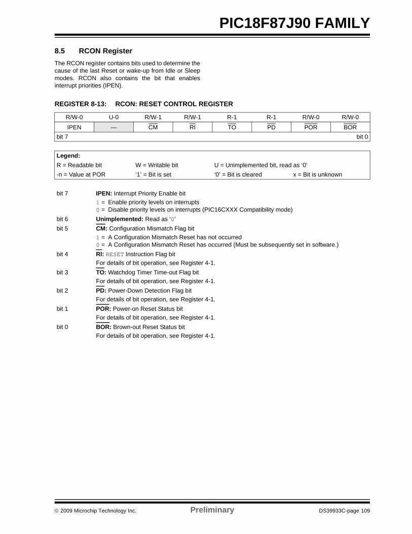
© 2009 Microchip Technology Inc. Preliminary DS39933C-page 109
PIC18F87J90 FAMILY8.5 RCON RegisterThe RCON register contains bits used to determine thecause of the last Reset or wake-up from Idle or Sleepmodes. RCON also contains the bit that enablesinterrupt priorities (IPEN).
REGISTER 8-13: RCON: RESET CONTROL REGISTER
R/W-0 U-0 R/W-1 R/W-1 R-1 R-1 R/W-0 R/W-0
IPEN — CM RI TO PD POR BORbit 7 bit 0
Legend:R = Readable bit W = Writable bit U = Unimplemented bit, read as ‘0’-n = Value at POR ‘1’ = Bit is set ‘0’ = Bit is cleared x = Bit is unknown
bit 7 IPEN: Interrupt Priority Enable bit 1 = Enable priority levels on interrupts0 = Disable priority levels on interrupts (PIC16CXXX Compatibility mode)
bit 6 Unimplemented: Read as ‘0’ bit 5 CM: Configuration Mismatch Flag bit
1 = A Configuration Mismatch Reset has not occurred0 = A Configuration Mismatch Reset has occurred (Must be subsequently set in software.)
bit 4 RI: RESET Instruction Flag bit For details of bit operation, see Register 4-1.
bit 3 TO: Watchdog Timer Time-out Flag bit For details of bit operation, see Register 4-1.
bit 2 PD: Power-Down Detection Flag bit For details of bit operation, see Register 4-1.
bit 1 POR: Power-on Reset Status bitFor details of bit operation, see Register 4-1.
bit 0 BOR: Brown-out Reset Status bit For details of bit operation, see Register 4-1.
PIC18F87J90 FAMILY
DS39933C-page 110 Preliminary © 2009 Microchip Technology Inc.
8.6 INTx Pin InterruptsExternal interrupts on the RB0/INT0, RB1/INT1,RB2/INT2 and RB3/INT3 pins are edge-triggered. If thecorresponding INTEDGx bit in the INTCON2 register isset (= 1), the interrupt is triggered by a rising edge; ifthe bit is clear, the trigger is on the falling edge. Whena valid edge appears on the RBx/INTx pin, thecorresponding flag bit, INTxIF, is set. This interrupt canbe disabled by clearing the corresponding enable bit,INTxIE. Flag bit, INTxIF, must be cleared in software inthe Interrupt Service Routine before re-enabling theinterrupt.
All external interrupts (INT0, INT1, INT2 and INT3) canwake-up the processor from the power-managedmodes if bit INTxIE was set prior to going into thepower-managed modes. If the Global Interrupt Enablebit, GIE, is set, the processor will branch to the interruptvector following wake-up.
Interrupt priority for INT1, INT2 and INT3 is determinedby the value contained in the interrupt priority bits,INT1IP (INTCON3<6>), INT2IP (INTCON3<7>) andINT3IP (INTCON2<1>). There is no priority bitassociated with INT0. It is always a high-priorityinterrupt source.
8.7 TMR0 InterruptIn 8-bit mode (which is the default), an overflow in theTMR0 register (FFh → 00h) will set flag bit, TMR0IF. In16-bit mode, an overflow in the TMR0H:TMR0L registerpair (FFFFh → 0000h) will set TMR0IF. The interrupt canbe enabled/disabled by setting/clearing enable bit,TMR0IE (INTCON<5>). Interrupt priority for Timer0 isdetermined by the value contained in the interrupt prioritybit, TMR0IP (INTCON2<2>). See Section 10.0 “Timer0Module” for further details on the Timer0 module.
8.8 PORTB Interrupt-on-ChangeAn input change on PORTB<7:4> sets flag bit, RBIF(INTCON<0>). The interrupt can be enabled/disabledby setting/clearing enable bit, RBIE (INTCON<3>).Interrupt priority for PORTB interrupt-on-change isdetermined by the value contained in the interruptpriority bit, RBIP (INTCON2<0>).
8.9 Context Saving During InterruptsDuring interrupts, the return PC address is saved onthe stack. Additionally, the WREG, STATUS and BSRregisters are saved on the Fast Return Stack. If a fastreturn from interrupt is not used (see Section 5.3“Data Memory Organization”), the user may need tosave the WREG, STATUS and BSR registers on entryto the Interrupt Service Routine. Depending on theuser’s application, other registers may also need to besaved. Example 8-1 saves and restores the WREG,STATUS and BSR registers during an Interrupt ServiceRoutine.
EXAMPLE 8-1: SAVING STATUS, WREG AND BSR REGISTERS IN RAM MOVWF W_TEMP ; W_TEMP is in virtual bankMOVFF STATUS, STATUS_TEMP ; STATUS_TEMP located anywhereMOVFF BSR, BSR_TEMP ; BSR_TMEP located anywhere;; USER ISR CODE;MOVFF BSR_TEMP, BSR ; Restore BSRMOVF W_TEMP, W ; Restore WREGMOVFF STATUS_TEMP, STATUS ; Restore STATUS
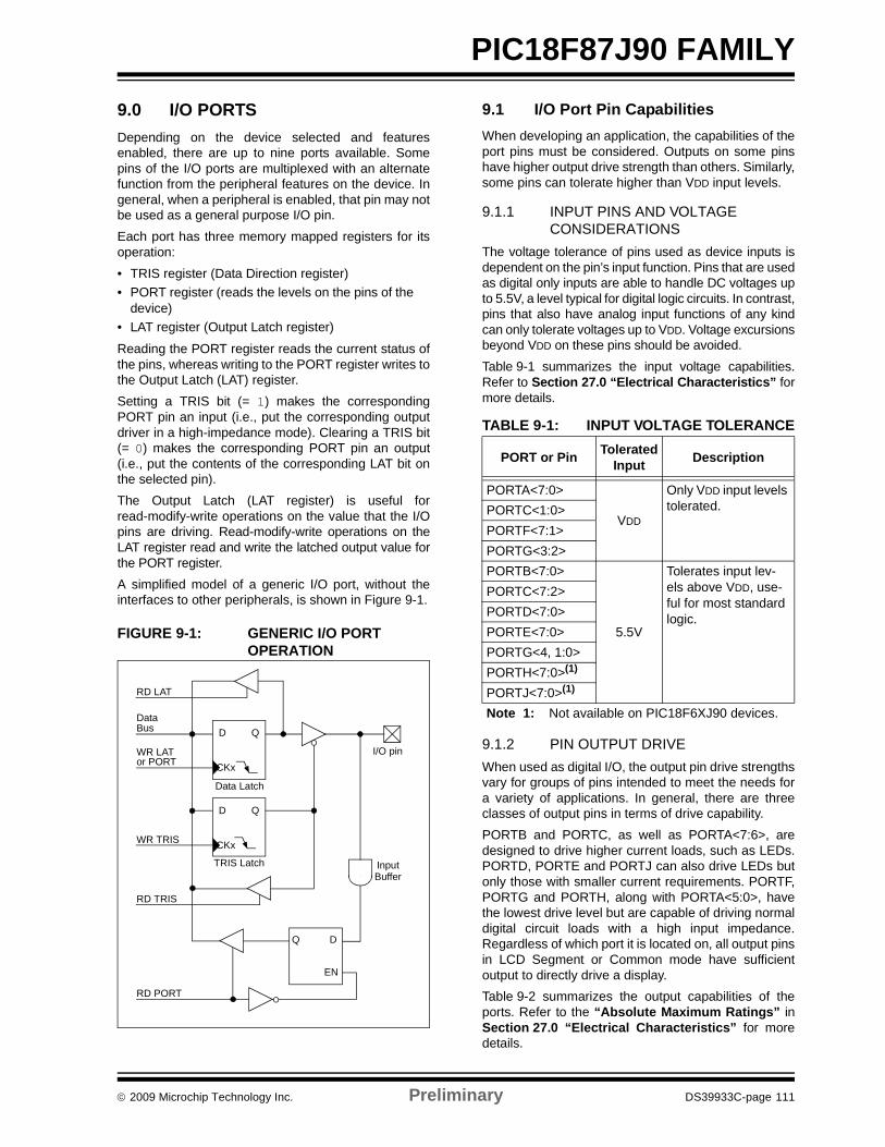
© 2009 Microchip Technology Inc. Preliminary DS39933C-page 111
PIC18F87J90 FAMILY
9.0 I/O PORTSDepending on the device selected and featuresenabled, there are up to nine ports available. Somepins of the I/O ports are multiplexed with an alternatefunction from the peripheral features on the device. Ingeneral, when a peripheral is enabled, that pin may notbe used as a general purpose I/O pin.Each port has three memory mapped registers for itsoperation:• TRIS register (Data Direction register)• PORT register (reads the levels on the pins of the
device)• LAT register (Output Latch register)
Reading the PORT register reads the current status ofthe pins, whereas writing to the PORT register writes tothe Output Latch (LAT) register. Setting a TRIS bit (= 1) makes the correspondingPORT pin an input (i.e., put the corresponding outputdriver in a high-impedance mode). Clearing a TRIS bit(= 0) makes the corresponding PORT pin an output(i.e., put the contents of the corresponding LAT bit onthe selected pin). The Output Latch (LAT register) is useful forread-modify-write operations on the value that the I/Opins are driving. Read-modify-write operations on theLAT register read and write the latched output value forthe PORT register.A simplified model of a generic I/O port, without theinterfaces to other peripherals, is shown in Figure 9-1.
FIGURE 9-1: GENERIC I/O PORT OPERATION
9.1 I/O Port Pin CapabilitiesWhen developing an application, the capabilities of theport pins must be considered. Outputs on some pinshave higher output drive strength than others. Similarly,some pins can tolerate higher than VDD input levels.
9.1.1 INPUT PINS AND VOLTAGE CONSIDERATIONS
The voltage tolerance of pins used as device inputs isdependent on the pin’s input function. Pins that are usedas digital only inputs are able to handle DC voltages upto 5.5V, a level typical for digital logic circuits. In contrast,pins that also have analog input functions of any kindcan only tolerate voltages up to VDD. Voltage excursionsbeyond VDD on these pins should be avoided. Table 9-1 summarizes the input voltage capabilities.Refer to Section 27.0 “Electrical Characteristics” formore details.
TABLE 9-1: INPUT VOLTAGE TOLERANCE
9.1.2 PIN OUTPUT DRIVEWhen used as digital I/O, the output pin drive strengthsvary for groups of pins intended to meet the needs fora variety of applications. In general, there are threeclasses of output pins in terms of drive capability.PORTB and PORTC, as well as PORTA<7:6>, aredesigned to drive higher current loads, such as LEDs.PORTD, PORTE and PORTJ can also drive LEDs butonly those with smaller current requirements. PORTF,PORTG and PORTH, along with PORTA<5:0>, havethe lowest drive level but are capable of driving normaldigital circuit loads with a high input impedance.Regardless of which port it is located on, all output pinsin LCD Segment or Common mode have sufficientoutput to directly drive a display.Table 9-2 summarizes the output capabilities of theports. Refer to the “Absolute Maximum Ratings” inSection 27.0 “Electrical Characteristics” for moredetails.
DataBus
WR LAT
WR TRIS
RD PORT
Data Latch
TRIS Latch
RD TRIS
InputBuffer
I/O pin
QD
CKx
QD
CKx
EN
Q D
EN
RD LAT
or PORT
PORT or Pin Tolerated Input Description
PORTA<7:0>
VDD
Only VDD input levels tolerated.PORTC<1:0>
PORTF<7:1>PORTG<3:2>PORTB<7:0>
5.5V
Tolerates input lev-els above VDD, use-ful for most standard logic.
PORTC<7:2>PORTD<7:0>PORTE<7:0>PORTG<4, 1:0>PORTH<7:0>(1)
PORTJ<7:0>(1)
Note 1: Not available on PIC18F6XJ90 devices.
PIC18F87J90 FAMILY
DS39933C-page 112 Preliminary © 2009 Microchip Technology Inc.
TABLE 9-2: OUTPUT DRIVE LEVELS FOR VARIOUS PORTS
9.1.3 PULL-UP CONFIGURATIONFour of the I/O ports (PORTB, PORTD, PORTE andPORTJ) implement configurable weak pull-ups on allpins. These are internal pull-ups that allow floatingdigital input signals to be pulled to a consistent levelwithout the use of external resistors.
The pull-ups are enabled with a single bit for each of theports: RBPU (INTCON2<7>) for PORTB, and RDPU,REPU and PJPU (PORTG<7:5>) for the other ports.
9.1.4 OPEN-DRAIN OUTPUTSThe output pins for several peripherals are alsoequipped with a configurable, open-drain output option.This allows the peripherals to communicate withexternal digital logic, operating at a higher voltagelevel, without the use of level translators.
The open-drain option is implemented on port pinsspecifically associated with the data and clock outputsof the USARTs, the MSSP module (in SPI mode) andthe CCP modules. This option is selectively enabled bysetting the open-drain control bit for the correspondingmodule in TRISG and LATG. Their configuration is dis-cussed in more detail in Section 9.4 “PORTC, TRISCand LATC Registers”, Section 9.6 “PORTE, TRISEand LATE Registers” and Section 9.8 “PORTG,TRISG and LATG Registers”.
When the open-drain option is required, the output pinmust also be tied through an external pull-up resistorprovided by the user to a higher voltage level, up to 5V(Figure 9-2). When a digital logic high signal is output,it is pulled up to the higher voltage level.
FIGURE 9-2: USING THE OPEN-DRAIN OUTPUT (USART SHOWN AS EXAMPLE)
9.2 PORTA, TRISA and LATA Registers
PORTA is an 8-bit wide, bidirectional port. The corre-sponding Data Direction and Output Latch registers areTRISA and LATA.
RA4/T0CKI is a Schmitt Trigger input. All other PORTApins have TTL input levels and full CMOS outputdrivers.
The RA4 pin is multiplexed with the Timer0 clock inputand one of the LCD segment drives. RA5 and RA<3:0>are multiplexed with analog inputs for the A/Dconverter.
The operation of the analog inputs as A/D converterinputs is selected by clearing or setting the PCFG<3:0>control bits in the ADCON1 register. The correspondingTRISA bits control the direction of these pins, evenwhen they are being used as analog inputs. The usermust ensure the bits in the TRISA register aremaintained set when using them as analog inputs.
OSC2/CLKO/RA6 and OSC1/CLKI/RA7 normallyserve as the external circuit connections for the exter-nal (primary) oscillator circuit (HS Oscillator modes), orthe external clock input and output (EC Oscillatormodes). In these cases, RA6 and RA7 are not availableas digital I/O and their corresponding TRIS and LATbits are read as ‘0’. When the device is configured touse INTOSC or INTRC as the default oscillator mode(FOSC2 Configuration bit is ‘0’), RA6 and RA7 areautomatically configured as digital I/O; the oscillatorand clock in/clock out functions are disabled.
RA1, RA4 and RA5 are multiplexed with LCD segmentdrives, controlled by bits in the LCDSE1 and LCDSE2registers. I/O port functionality is only available whenthe LCD segments are disabled.
EXAMPLE 9-1: INITIALIZING PORTA
Low Medium High
PORTA<5:0> PORTD PORTA<7:6>PORTF PORTE PORTBPORTG PORTJ(1) PORTCPORTH(1)
Note 1: Not available on PIC18F6XJ90 devices.
TXX
+5V
3.3V
(at logic ‘1’)
3.3V
VDD 5V
PIC18F87J90
Note: RA5 and RA<3:0> are configured asanalog inputs on any Reset and are readas ‘0’. RA4 is configured as a digital input.
CLRF PORTA ; Initialize PORTA by; clearing output latches
CLRF LATA ; Alternate method to; clear output data latches
MOVLW 07h ; Configure A/D MOVWF ADCON1 ; for digital inputsMOVLW 0BFh ; Value used to initialize
; data directionMOVWF TRISA ; Set RA<7, 5:0> as inputs,
; RA<6> as output
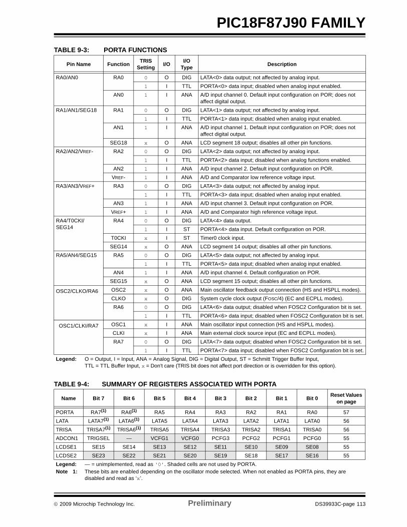
© 2009 Microchip Technology Inc. Preliminary DS39933C-page 113
PIC18F87J90 FAMILYTABLE 9-3: PORTA FUNCTIONS
TABLE 9-4: SUMMARY OF REGISTERS ASSOCIATED WITH PORTA
Pin Name Function TRIS Setting I/O I/O
Type Description
RA0/AN0 RA0 0 O DIG LATA<0> data output; not affected by analog input.1 I TTL PORTA<0> data input; disabled when analog input enabled.
AN0 1 I ANA A/D input channel 0. Default input configuration on POR; does not affect digital output.
RA1/AN1/SEG18 RA1 0 O DIG LATA<1> data output; not affected by analog input.1 I TTL PORTA<1> data input; disabled when analog input enabled.
AN1 1 I ANA A/D input channel 1. Default input configuration on POR; does not affect digital output.
SEG18 x O ANA LCD segment 18 output; disables all other pin functions.RA2/AN2/VREF- RA2 0 O DIG LATA<2> data output; not affected by analog input.
1 I TTL PORTA<2> data input; disabled when analog functions enabled.AN2 1 I ANA A/D input channel 2. Default input configuration on POR.
VREF- 1 I ANA A/D and Comparator low reference voltage input. RA3/AN3/VREF+ RA3 0 O DIG LATA<3> data output; not affected by analog input.
1 I TTL PORTA<3> data input; disabled when analog input enabled.AN3 1 I ANA A/D input channel 3. Default input configuration on POR.
VREF+ 1 I ANA A/D and Comparator high reference voltage input.RA4/T0CKI/SEG14
RA4 0 O DIG LATA<4> data output.1 I ST PORTA<4> data input. Default configuration on POR.
T0CKI x I ST Timer0 clock input.SEG14 x O ANA LCD segment 14 output; disables all other pin functions.
RA5/AN4/SEG15 RA5 0 O DIG LATA<5> data output; not affected by analog input.1 I TTL PORTA<5> data input; disabled when analog input enabled.
AN4 1 I ANA A/D input channel 4. Default configuration on POR.SEG15 x O ANA LCD segment 15 output; disables all other pin functions.
OSC2/CLKO/RA6 OSC2 x O ANA Main oscillator feedback output connection (HS and HSPLL modes).CLKO x O DIG System cycle clock output (FOSC/4) (EC and ECPLL modes).RA6 0 O DIG LATA<6> data output; disabled when FOSC2 Configuration bit is set.
1 I TTL PORTA<6> data input; disabled when FOSC2 Configuration bit is set.
OSC1/CLKI/RA7 OSC1 x I ANA Main oscillator input connection (HS and HSPLL modes).CLKI x I ANA Main external clock source input (EC and ECPLL modes).RA7 0 O DIG LATA<7> data output; disabled when FOSC2 Configuration bit is set.
1 I TTL PORTA<7> data input; disabled when FOSC2 Configuration bit is set.Legend: O = Output, I = Input, ANA = Analog Signal, DIG = Digital Output, ST = Schmitt Trigger Buffer Input,
TTL = TTL Buffer Input, x = Don’t care (TRIS bit does not affect port direction or is overridden for this option).
Name Bit 7 Bit 6 Bit 5 Bit 4 Bit 3 Bit 2 Bit 1 Bit 0 Reset Values on page
PORTA RA7(1) RA6(1) RA5 RA4 RA3 RA2 RA1 RA0 57LATA LATA7(1) LATA6(1) LATA5 LATA4 LATA3 LATA2 LATA1 LATA0 56TRISA TRISA7(1) TRISA6(1) TRISA5 TRISA4 TRISA3 TRISA2 TRISA1 TRISA0 56ADCON1 TRIGSEL — VCFG1 VCFG0 PCFG3 PCFG2 PCFG1 PCFG0 55LCDSE1 SE15 SE14 SE13 SE12 SE11 SE10 SE09 SE08 55LCDSE2 SE23 SE22 SE21 SE20 SE19 SE18 SE17 SE16 55Legend: — = unimplemented, read as ‘0’. Shaded cells are not used by PORTA.Note 1: These bits are enabled depending on the oscillator mode selected. When not enabled as PORTA pins, they are
disabled and read as ‘x’.
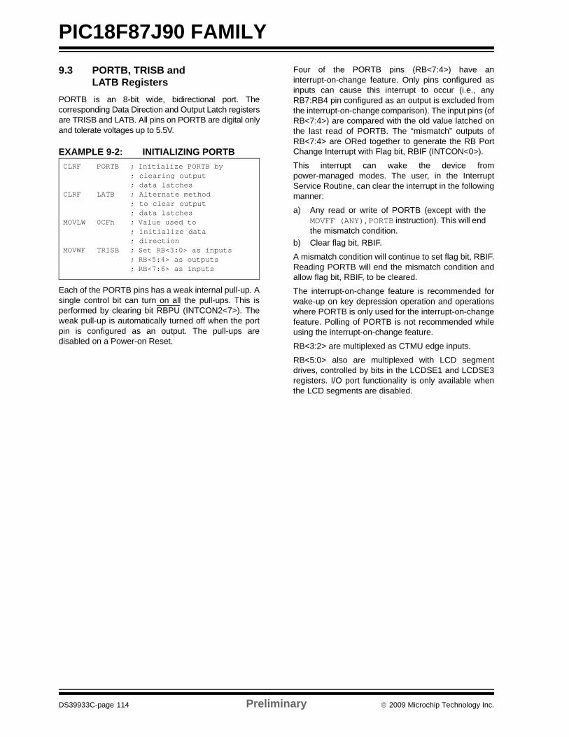
PIC18F87J90 FAMILY
DS39933C-page 114 Preliminary © 2009 Microchip Technology Inc.
9.3 PORTB, TRISB and LATB Registers
PORTB is an 8-bit wide, bidirectional port. Thecorresponding Data Direction and Output Latch registersare TRISB and LATB. All pins on PORTB are digital onlyand tolerate voltages up to 5.5V.
EXAMPLE 9-2: INITIALIZING PORTB
Each of the PORTB pins has a weak internal pull-up. Asingle control bit can turn on all the pull-ups. This isperformed by clearing bit RBPU (INTCON2<7>). Theweak pull-up is automatically turned off when the portpin is configured as an output. The pull-ups aredisabled on a Power-on Reset.
Four of the PORTB pins (RB<7:4>) have aninterrupt-on-change feature. Only pins configured asinputs can cause this interrupt to occur (i.e., anyRB7:RB4 pin configured as an output is excluded fromthe interrupt-on-change comparison). The input pins (ofRB<7:4>) are compared with the old value latched onthe last read of PORTB. The “mismatch” outputs ofRB<7:4> are ORed together to generate the RB PortChange Interrupt with Flag bit, RBIF (INTCON<0>).
This interrupt can wake the device frompower-managed modes. The user, in the InterruptService Routine, can clear the interrupt in the followingmanner:
a) Any read or write of PORTB (except with theMOVFF (ANY), PORTB instruction). This will endthe mismatch condition.
b) Clear flag bit, RBIF.
A mismatch condition will continue to set flag bit, RBIF.Reading PORTB will end the mismatch condition andallow flag bit, RBIF, to be cleared.
The interrupt-on-change feature is recommended forwake-up on key depression operation and operationswhere PORTB is only used for the interrupt-on-changefeature. Polling of PORTB is not recommended whileusing the interrupt-on-change feature.
RB<3:2> are multiplexed as CTMU edge inputs.
RB<5:0> also are multiplexed with LCD segmentdrives, controlled by bits in the LCDSE1 and LCDSE3registers. I/O port functionality is only available whenthe LCD segments are disabled.
CLRF PORTB ; Initialize PORTB by; clearing output; data latches
CLRF LATB ; Alternate method; to clear output; data latches
MOVLW 0CFh ; Value used to; initialize data ; direction
MOVWF TRISB ; Set RB<3:0> as inputs; RB<5:4> as outputs; RB<7:6> as inputs
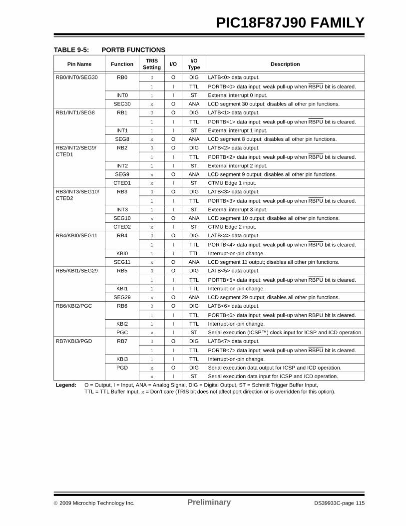
© 2009 Microchip Technology Inc. Preliminary DS39933C-page 115
PIC18F87J90 FAMILYTABLE 9-5: PORTB FUNCTIONS
Pin Name Function TRIS Setting I/O I/O
Type Description
RB0/INT0/SEG30 RB0 0 O DIG LATB<0> data output.
1 I TTL PORTB<0> data input; weak pull-up when RBPU bit is cleared.INT0 1 I ST External interrupt 0 input.
SEG30 x O ANA LCD segment 30 output; disables all other pin functions.RB1/INT1/SEG8 RB1 0 O DIG LATB<1> data output.
1 I TTL PORTB<1> data input; weak pull-up when RBPU bit is cleared.INT1 1 I ST External interrupt 1 input.SEG8 x O ANA LCD segment 8 output; disables all other pin functions.
RB2/INT2/SEG9/CTED1
RB2 0 O DIG LATB<2> data output.
1 I TTL PORTB<2> data input; weak pull-up when RBPU bit is cleared.INT2 1 I ST External interrupt 2 input.SEG9 x O ANA LCD segment 9 output; disables all other pin functions.
CTED1 x I ST CTMU Edge 1 input.RB3/INT3/SEG10/CTED2
RB3 0 O DIG LATB<3> data output.
1 I TTL PORTB<3> data input; weak pull-up when RBPU bit is cleared.INT3 1 I ST External interrupt 3 input.
SEG10 x O ANA LCD segment 10 output; disables all other pin functions.CTED2 x I ST CTMU Edge 2 input.
RB4/KBI0/SEG11 RB4 0 O DIG LATB<4> data output.
1 I TTL PORTB<4> data input; weak pull-up when RBPU bit is cleared.KBI0 1 I TTL Interrupt-on-pin change.
SEG11 x O ANA LCD segment 11 output; disables all other pin functions.RB5/KBI1/SEG29 RB5 0 O DIG LATB<5> data output.
1 I TTL PORTB<5> data input; weak pull-up when RBPU bit is cleared.KBI1 1 I TTL Interrupt-on-pin change.
SEG29 x O ANA LCD segment 29 output; disables all other pin functions.RB6/KBI2/PGC RB6 0 O DIG LATB<6> data output.
1 I TTL PORTB<6> data input; weak pull-up when RBPU bit is cleared.KBI2 1 I TTL Interrupt-on-pin change.PGC x I ST Serial execution (ICSP™) clock input for ICSP and ICD operation.
RB7/KBI3/PGD RB7 0 O DIG LATB<7> data output.
1 I TTL PORTB<7> data input; weak pull-up when RBPU bit is cleared.KBI3 1 I TTL Interrupt-on-pin change.PGD x O DIG Serial execution data output for ICSP and ICD operation.
x I ST Serial execution data input for ICSP and ICD operation.Legend: O = Output, I = Input, ANA = Analog Signal, DIG = Digital Output, ST = Schmitt Trigger Buffer Input,
TTL = TTL Buffer Input, x = Don’t care (TRIS bit does not affect port direction or is overridden for this option).
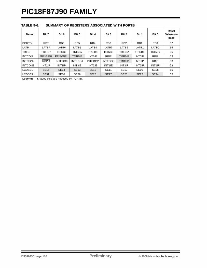
PIC18F87J90 FAMILY
DS39933C-page 116 Preliminary © 2009 Microchip Technology Inc.
TABLE 9-6: SUMMARY OF REGISTERS ASSOCIATED WITH PORTB
Name Bit 7 Bit 6 Bit 5 Bit 4 Bit 3 Bit 2 Bit 1 Bit 0Reset
Values on page
PORTB RB7 RB6 RB5 RB4 RB3 RB2 RB1 RB0 57LATB LATB7 LATB6 LATB5 LATB4 LATB3 LATB2 LATB1 LATB0 56TRISB TRISB7 TRISB6 TRISB5 TRISB4 TRISB3 TRISB2 TRISB1 TRISB0 56INTCON GIE/GIEH PEIE/GIEL TMR0IE INT0IE RBIE TMR0IF INT0IF RBIF 53
INTCON2 RBPU INTEDG0 INTEDG1 INTEDG2 INTEDG3 TMR0IP INT3IP RBIP 53INTCON3 INT2IP INT1IP INT3IE INT2IE INT1IE INT3IF INT2IF INT1IF 53LCDSE1 SE15 SE14 SE13 SE12 SE11 SE10 SE09 SE08 55LCDSE3 SE31 SE30 SE29 SE28 SE27 SE26 SE25 SE24 55Legend: Shaded cells are not used by PORTB.
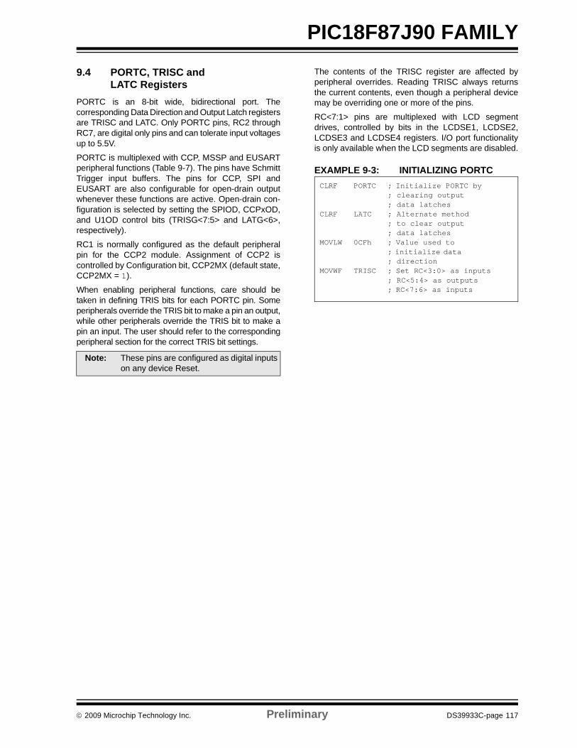
© 2009 Microchip Technology Inc. Preliminary DS39933C-page 117
PIC18F87J90 FAMILY
9.4 PORTC, TRISC and LATC Registers
PORTC is an 8-bit wide, bidirectional port. Thecorresponding Data Direction and Output Latch registersare TRISC and LATC. Only PORTC pins, RC2 throughRC7, are digital only pins and can tolerate input voltagesup to 5.5V.
PORTC is multiplexed with CCP, MSSP and EUSARTperipheral functions (Table 9-7). The pins have SchmittTrigger input buffers. The pins for CCP, SPI andEUSART are also configurable for open-drain outputwhenever these functions are active. Open-drain con-figuration is selected by setting the SPIOD, CCPxOD,and U1OD control bits (TRISG<7:5> and LATG<6>,respectively).
RC1 is normally configured as the default peripheralpin for the CCP2 module. Assignment of CCP2 iscontrolled by Configuration bit, CCP2MX (default state,CCP2MX = 1).
When enabling peripheral functions, care should betaken in defining TRIS bits for each PORTC pin. Someperipherals override the TRIS bit to make a pin an output,while other peripherals override the TRIS bit to make apin an input. The user should refer to the correspondingperipheral section for the correct TRIS bit settings.
The contents of the TRISC register are affected byperipheral overrides. Reading TRISC always returnsthe current contents, even though a peripheral devicemay be overriding one or more of the pins.
RC<7:1> pins are multiplexed with LCD segmentdrives, controlled by bits in the LCDSE1, LCDSE2,LCDSE3 and LCDSE4 registers. I/O port functionalityis only available when the LCD segments are disabled.
EXAMPLE 9-3: INITIALIZING PORTC
Note: These pins are configured as digital inputson any device Reset.
CLRF PORTC ; Initialize PORTC by; clearing output; data latches
CLRF LATC ; Alternate method; to clear output; data latches
MOVLW 0CFh ; Value used to ; initialize data ; direction
MOVWF TRISC ; Set RC<3:0> as inputs; RC<5:4> as outputs; RC<7:6> as inputs
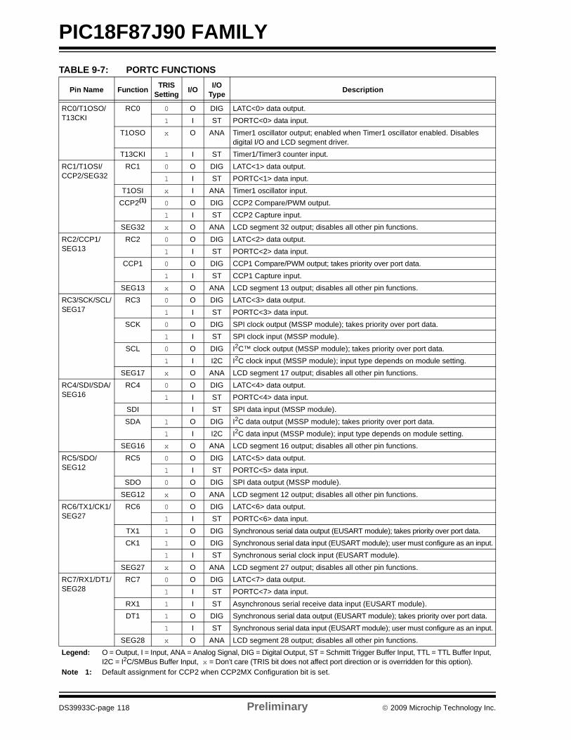
PIC18F87J90 FAMILY
DS39933C-page 118 Preliminary © 2009 Microchip Technology Inc.
TABLE 9-7: PORTC FUNCTIONS
Pin Name Function TRIS Setting I/O I/O
Type Description
RC0/T1OSO/T13CKI
RC0 0 O DIG LATC<0> data output.1 I ST PORTC<0> data input.
T1OSO x O ANA Timer1 oscillator output; enabled when Timer1 oscillator enabled. Disables digital I/O and LCD segment driver.
T13CKI 1 I ST Timer1/Timer3 counter input.RC1/T1OSI/CCP2/SEG32
RC1 0 O DIG LATC<1> data output.1 I ST PORTC<1> data input.
T1OSI x I ANA Timer1 oscillator input.CCP2(1) 0 O DIG CCP2 Compare/PWM output.
1 I ST CCP2 Capture input.SEG32 x O ANA LCD segment 32 output; disables all other pin functions.
RC2/CCP1/SEG13
RC2 0 O DIG LATC<2> data output.1 I ST PORTC<2> data input.
CCP1 0 O DIG CCP1 Compare/PWM output; takes priority over port data.1 I ST CCP1 Capture input.
SEG13 x O ANA LCD segment 13 output; disables all other pin functions.RC3/SCK/SCL/SEG17
RC3 0 O DIG LATC<3> data output.1 I ST PORTC<3> data input.
SCK 0 O DIG SPI clock output (MSSP module); takes priority over port data.1 I ST SPI clock input (MSSP module).
SCL 0 O DIG I2C™ clock output (MSSP module); takes priority over port data.1 I I2C I2C clock input (MSSP module); input type depends on module setting.
SEG17 x O ANA LCD segment 17 output; disables all other pin functions.RC4/SDI/SDA/SEG16
RC4 0 O DIG LATC<4> data output.1 I ST PORTC<4> data input.
SDI I ST SPI data input (MSSP module).SDA 1 O DIG I2C data output (MSSP module); takes priority over port data.
1 I I2C I2C data input (MSSP module); input type depends on module setting.SEG16 x O ANA LCD segment 16 output; disables all other pin functions.
RC5/SDO/SEG12
RC5 0 O DIG LATC<5> data output.1 I ST PORTC<5> data input.
SDO 0 O DIG SPI data output (MSSP module).SEG12 x O ANA LCD segment 12 output; disables all other pin functions.
RC6/TX1/CK1/SEG27
RC6 0 O DIG LATC<6> data output.1 I ST PORTC<6> data input.
TX1 1 O DIG Synchronous serial data output (EUSART module); takes priority over port data.CK1 1 O DIG Synchronous serial data input (EUSART module); user must configure as an input.
1 I ST Synchronous serial clock input (EUSART module).SEG27 x O ANA LCD segment 27 output; disables all other pin functions.
RC7/RX1/DT1/SEG28
RC7 0 O DIG LATC<7> data output.1 I ST PORTC<7> data input.
RX1 1 I ST Asynchronous serial receive data input (EUSART module).DT1 1 O DIG Synchronous serial data output (EUSART module); takes priority over port data.
1 I ST Synchronous serial data input (EUSART module); user must configure as an input.SEG28 x O ANA LCD segment 28 output; disables all other pin functions.
Legend: O = Output, I = Input, ANA = Analog Signal, DIG = Digital Output, ST = Schmitt Trigger Buffer Input, TTL = TTL Buffer Input, I2C = I2C/SMBus Buffer Input, x = Don’t care (TRIS bit does not affect port direction or is overridden for this option).
Note 1: Default assignment for CCP2 when CCP2MX Configuration bit is set.
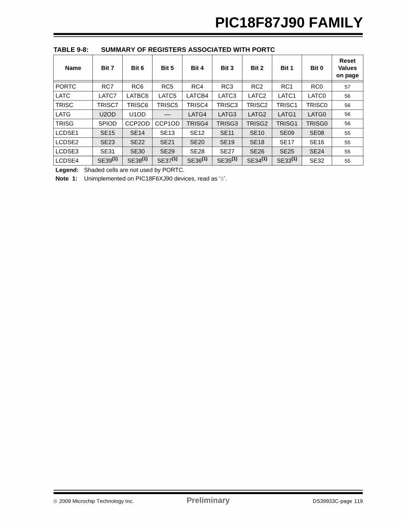
© 2009 Microchip Technology Inc. Preliminary DS39933C-page 119
PIC18F87J90 FAMILYTABLE 9-8: SUMMARY OF REGISTERS ASSOCIATED WITH PORTC
Name Bit 7 Bit 6 Bit 5 Bit 4 Bit 3 Bit 2 Bit 1 Bit 0Reset Values
on page
PORTC RC7 RC6 RC5 RC4 RC3 RC2 RC1 RC0 57
LATC LATC7 LATBC6 LATC5 LATCB4 LATC3 LATC2 LATC1 LATC0 56
TRISC TRISC7 TRISC6 TRISC5 TRISC4 TRISC3 TRISC2 TRISC1 TRISC0 56
LATG U2OD U1OD — LATG4 LATG3 LATG2 LATG1 LATG0 56
TRISG SPIOD CCP2OD CCP1OD TRISG4 TRISG3 TRISG2 TRISG1 TRISG0 56
LCDSE1 SE15 SE14 SE13 SE12 SE11 SE10 SE09 SE08 55
LCDSE2 SE23 SE22 SE21 SE20 SE19 SE18 SE17 SE16 55
LCDSE3 SE31 SE30 SE29 SE28 SE27 SE26 SE25 SE24 55
LCDSE4 SE39(1) SE38(1) SE37(1) SE36(1) SE35(1) SE34(1) SE33(1) SE32 55
Legend: Shaded cells are not used by PORTC.Note 1: Unimplemented on PIC18F6XJ90 devices, read as ‘0’.
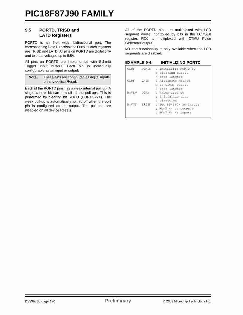
PIC18F87J90 FAMILY
DS39933C-page 120 Preliminary © 2009 Microchip Technology Inc.
9.5 PORTD, TRISD and LATD Registers
PORTD is an 8-bit wide, bidirectional port. Thecorresponding Data Direction and Output Latch registersare TRISD and LATD. All pins on PORTD are digital onlyand tolerate voltages up to 5.5V.
All pins on PORTD are implemented with SchmittTrigger input buffers. Each pin is individuallyconfigurable as an input or output.
Each of the PORTD pins has a weak internal pull-up. Asingle control bit can turn off all the pull-ups. This isperformed by clearing bit RDPU (PORTG<7>). Theweak pull-up is automatically turned off when the portpin is configured as an output. The pull-ups aredisabled on all device Resets.
All of the PORTD pins are multiplexed with LCDsegment drives, controlled by bits in the LCDSE0register. RD0 is multiplexed with CTMU PulseGenerator output.
I/O port functionality is only available when the LCDsegments are disabled.
EXAMPLE 9-4: INITIALIZING PORTD
Note: These pins are configured as digital inputson any device Reset.
CLRF PORTD ; Initialize PORTD by ; clearing output ; data latchesCLRF LATD ; Alternate method
; to clear output; data latches
MOVLW 0CFh ; Value used to ; initialize data ; direction
MOVWF TRISD ; Set RD<3:0> as inputs; RD<5:4> as outputs; RD<7:6> as inputs
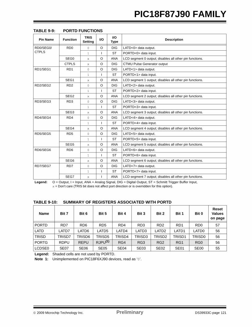
© 2009 Microchip Technology Inc. Preliminary DS39933C-page 121
PIC18F87J90 FAMILYTABLE 9-9: PORTD FUNCTIONS
TABLE 9-10: SUMMARY OF REGISTERS ASSOCIATED WITH PORTD
Pin Name Function TRIS Setting I/O I/O
Type Description
RD0/SEG0/CTPLS
RD0 0 O DIG LATD<0> data output.1 I ST PORTD<0> data input.
SEG0 x O ANA LCD segment 0 output; disables all other pin functions.CTPLS x O DIG CTMU Pulse Generator output
RD1/SEG1 RD1 0 O DIG LATD<1> data output.1 I ST PORTD<1> data input.
SEG1 x O ANA LCD segment 1 output; disables all other pin functions.RD2/SEG2 RD2 0 O DIG LATD<2> data output.
1 I ST PORTD<2> data input.SEG2 x O ANA LCD segment 2 output; disables all other pin functions.
RD3/SEG3 RD3 0 O DIG LATD<3> data output.1 I ST PORTD<3> data input.
SEG3 x O ANA LCD segment 3 output; disables all other pin functions.RD4/SEG4 RD4 0 O DIG LATD<4> data output.
1 I ST PORTD<4> data input.SEG4 x O ANA LCD segment 4 output; disables all other pin functions.
RD5/SEG5 RD5 0 O DIG LATD<5> data output.1 I ST PORTD<5> data input.
SEG5 x O ANA LCD segment 5 output; disables all other pin functions.RD6/SEG6 RD6 0 O DIG LATD<6> data output.
1 I ST PORTD<6> data input.SEG6 x O ANA LCD segment 6 output; disables all other pin functions.
RD7/SEG7 RD7 0 O DIG LATD<7> data output.1 I ST PORTD<7> data input.
SEG7 x I ANA LCD segment 7 output; disables all other pin functions.Legend: O = Output, I = Input, ANA = Analog Signal, DIG = Digital Output, ST = Schmitt Trigger Buffer Input,
x = Don’t care (TRIS bit does not affect port direction or is overridden for this option).
Name Bit 7 Bit 6 Bit 5 Bit 4 Bit 3 Bit 2 Bit 1 Bit 0Reset Values
on page
PORTD RD7 RD6 RD5 RD4 RD3 RD2 RD1 RD0 57LATD LATD7 LATD6 LATD5 LATD4 LATD3 LATD2 LATD1 LATD0 56TRISD TRISD7 TRISD6 TRISD5 TRISD4 TRISD3 TRISD2 TRISD1 TRISD0 56PORTG RDPU REPU RJPU(1) RG4 RG3 RG2 RG1 RG0 56LCDSE0 SE07 SE06 SE05 SE04 SE03 SE02 SE01 SE00 55Legend: Shaded cells are not used by PORTD.Note 1: Unimplemented on PIC18F6XJ90 devices, read as ‘0’.
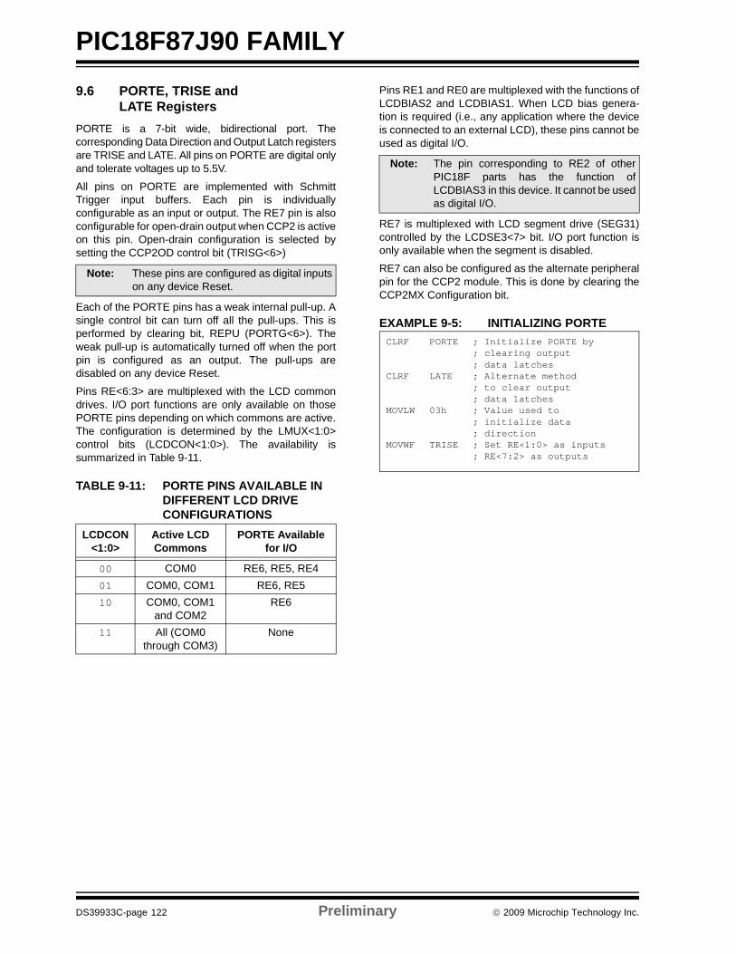
PIC18F87J90 FAMILY
DS39933C-page 122 Preliminary © 2009 Microchip Technology Inc.
9.6 PORTE, TRISE and LATE Registers
PORTE is a 7-bit wide, bidirectional port. Thecorresponding Data Direction and Output Latch registersare TRISE and LATE. All pins on PORTE are digital onlyand tolerate voltages up to 5.5V.
All pins on PORTE are implemented with SchmittTrigger input buffers. Each pin is individuallyconfigurable as an input or output. The RE7 pin is alsoconfigurable for open-drain output when CCP2 is activeon this pin. Open-drain configuration is selected bysetting the CCP2OD control bit (TRISG<6>)
Each of the PORTE pins has a weak internal pull-up. Asingle control bit can turn off all the pull-ups. This isperformed by clearing bit, REPU (PORTG<6>). Theweak pull-up is automatically turned off when the portpin is configured as an output. The pull-ups aredisabled on any device Reset.
Pins RE<6:3> are multiplexed with the LCD commondrives. I/O port functions are only available on thosePORTE pins depending on which commons are active.The configuration is determined by the LMUX<1:0>control bits (LCDCON<1:0>). The availability issummarized in Table 9-11.
TABLE 9-11: PORTE PINS AVAILABLE IN DIFFERENT LCD DRIVE CONFIGURATIONS
Pins RE1 and RE0 are multiplexed with the functions ofLCDBIAS2 and LCDBIAS1. When LCD bias genera-tion is required (i.e., any application where the deviceis connected to an external LCD), these pins cannot beused as digital I/O.
RE7 is multiplexed with LCD segment drive (SEG31)controlled by the LCDSE3<7> bit. I/O port function isonly available when the segment is disabled.
RE7 can also be configured as the alternate peripheralpin for the CCP2 module. This is done by clearing theCCP2MX Configuration bit.
EXAMPLE 9-5: INITIALIZING PORTE
Note: These pins are configured as digital inputson any device Reset.
LCDCON<1:0>
Active LCD Commons
PORTE Available for I/O
00 COM0 RE6, RE5, RE401 COM0, COM1 RE6, RE510 COM0, COM1
and COM2RE6
11 All (COM0 through COM3)
None
Note: The pin corresponding to RE2 of otherPIC18F parts has the function ofLCDBIAS3 in this device. It cannot be usedas digital I/O.
CLRF PORTE ; Initialize PORTE by; clearing output; data latches
CLRF LATE ; Alternate method; to clear output; data latches
MOVLW 03h ; Value used to ; initialize data ; direction
MOVWF TRISE ; Set RE<1:0> as inputs; RE<7:2> as outputs
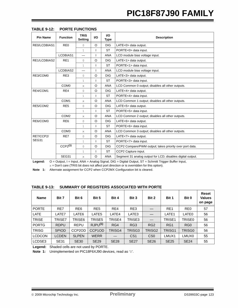
© 2009 Microchip Technology Inc. Preliminary DS39933C-page 123
PIC18F87J90 FAMILYTABLE 9-12: PORTE FUNCTIONS
TABLE 9-13: SUMMARY OF REGISTERS ASSOCIATED WITH PORTE
Pin Name Function TRIS Setting I/O I/O
Type Description
RE0/LCDBIAS1 RE0 0 O DIG LATE<0> data output.1 I ST PORTE<0> data input.
LCDBIAS1 — I ANA LCD module bias voltage input.RE1/LCDBIAS2 RE1 0 O DIG LATE<1> data output.
1 I ST PORTE<1> data input.LCDBIAS2 — I ANA LCD module bias voltage input.
RE3/COM0 RE3 0 O DIG LATE<3> data output.1 I ST PORTE<3> data input.
COM0 x O ANA LCD Common 0 output; disables all other outputs.RE4/COM1 RE4 0 O DIG LATE<4> data output.
1 I ST PORTE<4> data input.COM1 x O ANA LCD Common 1 output; disables all other outputs.
RE5/COM2 RE5 0 O DIG LATE<5> data output.1 I ST PORTE<5> data input.
COM2 x O ANA LCD Common 2 output; disables all other outputs.RE6/COM3 RE6 0 O DIG LATE<6> data output.
1 I ST PORTE<6> data input.COM3 x O ANA LCD Common 3 output; disables all other outputs.
RE7/CCP2/SEG31
RE7 0 O DIG LATE<7> data output.1 I ST PORTE<7> data input.
CCP2(1) 0 O DIG CCP2 Compare/PWM output; takes priority over port data.1 I ST CCP2 Capture input.
SEG31 x O ANA Segment 31 analog output for LCD; disables digital output.Legend: O = Output, I = Input, ANA = Analog Signal, DIG = Digital Output, ST = Schmitt Trigger Buffer Input,
x = Don’t care (TRIS bit does not affect port direction or is overridden for this option).Note 1: Alternate assignment for CCP2 when CCP2MX Configuration bit is cleared.
Name Bit 7 Bit 6 Bit 5 Bit 4 Bit 3 Bit 2 Bit 1 Bit 0Reset Values
on page
PORTE RE7 RE6 RE5 RE4 RE3 — RE1 RE0 57LATE LATE7 LATE6 LATE5 LATE4 LATE3 — LATE1 LATE0 56TRISE TRISE7 TRISE6 TRISE5 TRISE4 TRISE3 — TRISE1 TRISE0 56PORTG RDPU REPU RJPU(1) RG4 RG3 RG2 RG1 RG0 56TRISG SPIOD CCP2OD CCP1OD TRISG4 TRISG3 TRISG2 TRISG1 TRISG0 56LCDCON LCDEN SLPEN WERR — CS1 CS0 LMUX1 LMUX0 55LCDSE3 SE31 SE30 SE29 SE28 SE27 SE26 SE25 SE24 55Legend: Shaded cells are not used by PORTE.Note 1: Unimplemented on PIC18F6XJ90 devices, read as ‘0’.
PIC18F87J90 FAMILY
DS39933C-page 124 Preliminary © 2009 Microchip Technology Inc.
9.7 PORTF, LATF and TRISF RegistersPORTF is a 7-bit wide, bidirectional port. Thecorresponding Data Direction and Output Latch registersare TRISF and LATF. All pins on PORTF areimplemented with Schmitt Trigger input buffers. Each pinis individually configurable as an input or output.
PORTF is multiplexed with analog peripheral functions,as well as LCD segments. Pins RF1 through RF6 maybe used as comparator inputs or outputs by setting theappropriate bits in the CMCON register. To useRF<6:3> as digital inputs, it is also necessary to turn offthe comparators.
PORTF is also multiplexed with LCD segment drivescontrolled by bits in the LCDSE2 and LCDSE3registers. I/O port functions are only available when thesegments are disabled.
EXAMPLE 9-6: INITIALIZING PORTF
Note 1: On device Resets, pins RF6:RF1 areconfigured as analog inputs and are readas ‘0’.
2: To configure PORTF as digital I/O, turn offcomparators and set ADCON1 value.
CLRF PORTF ; Initialize PORTF by; clearing output; data latches
CLRF LATF ; Alternate method; to clear output; data latches
MOVLW 07h ; MOVWF CMCON ; Turn off comparatorsMOVLW 0Fh ; MOVWF ADCON1 ; Set PORTF as digital I/OMOVLW 0CEh ; Value used to
; initialize data ; direction
MOVWF TRISF ; Set RF3:RF1 as inputs; RF5:RF4 as outputs ; RF7:RF6 as inputs
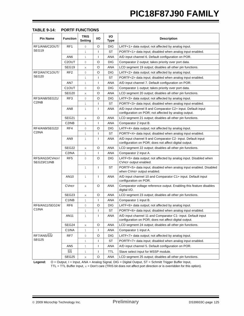
© 2009 Microchip Technology Inc. Preliminary DS39933C-page 125
PIC18F87J90 FAMILYTABLE 9-14: PORTF FUNCTIONS
Pin Name Function TRIS Setting I/O I/O
Type Description
RF1/AN6/C2OUT/SEG19
RF1 0 O DIG LATF<1> data output; not affected by analog input.1 I ST PORTF<1> data input; disabled when analog input enabled.
AN6 1 I ANA A/D input channel 6. Default configuration on POR.C2OUT 0 O DIG Comparator 2 output; takes priority over port data. SEG19 x O ANA LCD segment 19 output; disables all other pin functions.
RF2/AN7/C1OUT/SEG20
RF2 0 O DIG LATF<2> data output; not affected by analog input. 1 I ST PORTF<2> data input; disabled when analog input enabled.
AN7 1 I ANA A/D input channel 7. Default configuration on POR.C1OUT 0 O DIG Comparator 1 output; takes priority over port data. SEG20 x O ANA LCD segment 20 output; disables all other pin functions.
RF3/AN8/SEG21/C2INB
RF3 0 O DIG LATF<3> data output; not affected by analog input. 1 I ST PORTF<3> data input; disabled when analog input enabled.
AN8 1 I ANA A/D input channel 8 and Comparator C2+ input. Default input configuration on POR; not affected by analog output.
SEG21 x O ANA LCD segment 21 output; disables all other pin functions.C2INB 1 I ANA Comparator 2 input B.
RF4/AN9/SEG22/C2INA
RF4 0 O DIG LATF<4> data output; not affected by analog input.1 I ST PORTF<4> data input; disabled when analog input enabled.
AN9 1 I ANA A/D input channel 9 and Comparator C2- input. Default input configuration on POR; does not affect digital output.
SEG22 x O ANA LCD segment 22 output; disables all other pin functions.C2INA 1 I ANA Comparator 2 input A.
RF5/AN10/CVREF/SEG23/C1INB
RF5 0 O DIG LATF<5> data output; not affected by analog input. Disabled when CVREF output enabled.
1 I ST PORTF<5> data input; disabled when analog input enabled. Disabled when CVREF output enabled.
AN10 1 I ANA A/D input channel 10 and Comparator C1+ input. Default input configuration on POR.
CVREF x O ANA Comparator voltage reference output. Enabling this feature disables digital I/O.
SEG23 x O ANA LCD segment 23 output; disables all other pin functions.C1INB 1 I ANA Comparator 1 input B.
RF6/AN11/SEG24/C1INA
RF6 0 O DIG LATF<6> data output; not affected by analog input.1 I ST PORTF<6> data input; disabled when analog input enabled.
AN11 1 I ANA A/D input channel 11 and Comparator C1- input. Default input configuration on POR; does not affect digital output.
SEG24 x O ANA LCD segment 24 output; disables all other pin functions.C1INA 1 I ANA Comparator 1 input A.
RF7/AN5/SS/SEG25
RF7 0 O DIG LATF<7> data output; not affected by analog input. 1 I ST PORTF<7> data input; disabled when analog input enabled.
AN5 1 I ANA A/D input channel 5. Default configuration on POR.
SS 1 I TTL Slave select input for MSSP module.SEG25 x O ANA LCD segment 25 output; disables all other pin functions.
Legend: O = Output, I = Input, ANA = Analog Signal, DIG = Digital Output, ST = Schmitt Trigger Buffer Input, TTL = TTL Buffer Input, x = Don’t care (TRIS bit does not affect port direction or is overridden for this option).

PIC18F87J90 FAMILY
DS39933C-page 126 Preliminary © 2009 Microchip Technology Inc.
TABLE 9-15: SUMMARY OF REGISTERS ASSOCIATED WITH PORTF
Name Bit 7 Bit 6 Bit 5 Bit 4 Bit 3 Bit 2 Bit 1 Bit 0Reset Values
on page
PORTF RF7 RF6 RF5 RF4 RF3 RF2 RF1 — 56LATF LATF7 LATF6 LATF5 LATF4 LATF3 LATF2 LATF1 — 56TRISF TRISF7 TRISF6 TRISF5 TRISF4 TRISF3 TRISF2 TRISF1 — 56ADCON1 TRIGSEL — VCFG1 VCFG0 PCFG3 PCFG2 PCFG1 PCFG0 55CMCON C2OUT C1OUT C2INV C1INV CIS CM2 CM1 CM0 55CVRCON CVREN CVROE CVRR CVRSS CVR3 CVR2 CVR1 CVR0 55LCDSE2 SE23 SE22 SE21 SE20 SE19 SE18 SE17 SE16 55LCDSE3 SE31 SE30 SE29 SE28 SE27 SE26 SE25 SE24 55Legend: — = unimplemented, read as ‘0’. Shaded cells are not used by PORTF.
© 2009 Microchip Technology Inc. Preliminary DS39933C-page 127
PIC18F87J90 FAMILY9.8 PORTG, TRISG and
LATG RegistersPORTG is a 5-bit wide, bidirectional port. Thecorresponding Data Direction and Output Latch registersare TRISG and LATG. All pins on PORTG are digital onlyand tolerate voltages up to 5.5V.
PORTG is multiplexed with both AUSART and LCDfunctions (Table 9-16). When operating as I/O, allPORTG pins have Schmitt Trigger input buffers. TheRG1 pin is also configurable for open-drain outputwhen the AUSART is active. Open-drain configurationis selected by setting the U2OD control bit (LATG<7>).
RG4 is multiplexed with LCD segment drives controlledby bits in the LCDSE2 register and as the RTCC pin.The I/O port function is only available when thesegments are disabled.
RG3 and RG2 are multiplexed with VLCAP pins for theLCD charge pump, and RG0 is multiplexed withLCDBIAS0 bias voltage input. When these pins areused for LCD bias generation, the I/O and otherfunctions are unavailable.
When enabling peripheral functions, care should betaken in defining TRIS bits for each PORTG pin. Someperipherals override the TRIS bit to make a pin anoutput, while other peripherals override the TRIS bit tomake a pin an input. The user should refer to thecorresponding peripheral section for the correct TRIS bitsettings. The pin override value is not loaded into theTRIS register. This allows read-modify-write of the TRISregister without concern due to peripheral overrides.
Although the port itself is only five bits wide, thePORTG<7:5> bits are still implemented to control theweak pull-ups on the I/O ports associated with PORTD,PORTE and PORTJ. Setting these bits enables therespective port pull-ups.
Most of the corresponding TRISG and LATG bits areimplemented as open-drain control bits for CCP1,CCP2 and SPI (TRISG<7:5>), and the USARTs(LATG<7:6>). Setting these bits configures the outputpin for the corresponding peripheral for open-drainoperation. LATG<5> is not implemented.
EXAMPLE 9-7: INITIALIZING PORTG CLRF PORTG ; Initialize PORTG by
; clearing output; data latches
CLRF LATG ; Alternate method; to clear output; data latches
MOVLW 04h ; Value used to ; initialize data ; direction
MOVWF TRISG ; Set RG1:RG0 as outputs; RG2 as input; RG4:RG3 as inputs
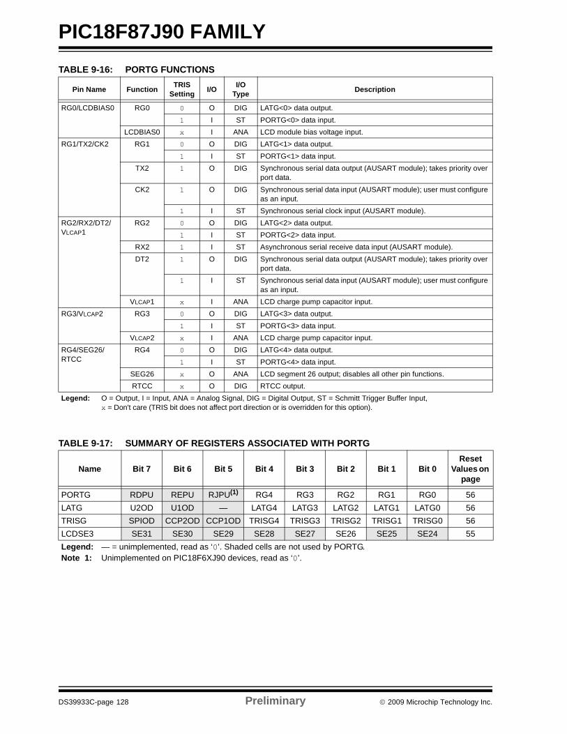
PIC18F87J90 FAMILY
DS39933C-page 128 Preliminary © 2009 Microchip Technology Inc.
TABLE 9-16: PORTG FUNCTIONS
TABLE 9-17: SUMMARY OF REGISTERS ASSOCIATED WITH PORTG
Pin Name Function TRIS Setting I/O I/O
Type Description
RG0/LCDBIAS0 RG0 0 O DIG LATG<0> data output.1 I ST PORTG<0> data input.
LCDBIAS0 x I ANA LCD module bias voltage input.RG1/TX2/CK2 RG1 0 O DIG LATG<1> data output.
1 I ST PORTG<1> data input.TX2 1 O DIG Synchronous serial data output (AUSART module); takes priority over
port data.CK2 1 O DIG Synchronous serial data input (AUSART module); user must configure
as an input.1 I ST Synchronous serial clock input (AUSART module).
RG2/RX2/DT2/VLCAP1
RG2 0 O DIG LATG<2> data output.1 I ST PORTG<2> data input.
RX2 1 I ST Asynchronous serial receive data input (AUSART module).DT2 1 O DIG Synchronous serial data output (AUSART module); takes priority over
port data.1 I ST Synchronous serial data input (AUSART module); user must configure
as an input.VLCAP1 x I ANA LCD charge pump capacitor input.
RG3/VLCAP2 RG3 0 O DIG LATG<3> data output.1 I ST PORTG<3> data input.
VLCAP2 x I ANA LCD charge pump capacitor input.RG4/SEG26/RTCC
RG4 0 O DIG LATG<4> data output.1 I ST PORTG<4> data input.
SEG26 x O ANA LCD segment 26 output; disables all other pin functions.RTCC x O DIG RTCC output.
Legend: O = Output, I = Input, ANA = Analog Signal, DIG = Digital Output, ST = Schmitt Trigger Buffer Input, x = Don’t care (TRIS bit does not affect port direction or is overridden for this option).
Name Bit 7 Bit 6 Bit 5 Bit 4 Bit 3 Bit 2 Bit 1 Bit 0Reset
Values on page
PORTG RDPU REPU RJPU(1) RG4 RG3 RG2 RG1 RG0 56LATG U2OD U1OD — LATG4 LATG3 LATG2 LATG1 LATG0 56TRISG SPIOD CCP2OD CCP1OD TRISG4 TRISG3 TRISG2 TRISG1 TRISG0 56LCDSE3 SE31 SE30 SE29 SE28 SE27 SE26 SE25 SE24 55Legend: — = unimplemented, read as ‘0’. Shaded cells are not used by PORTG.Note 1: Unimplemented on PIC18F6XJ90 devices, read as ‘0’.
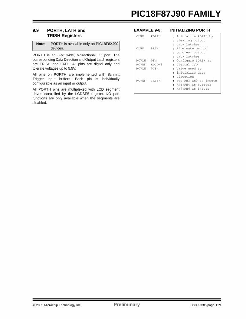
© 2009 Microchip Technology Inc. Preliminary DS39933C-page 129
PIC18F87J90 FAMILY9.9 PORTH, LATH and
TRISH Registers
PORTH is an 8-bit wide, bidirectional I/O port. Thecorresponding Data Direction and Output Latch registersare TRISH and LATH. All pins are digital only andtolerate voltages up to 5.5V.
All pins on PORTH are implemented with SchmittTrigger input buffers. Each pin is individuallyconfigurable as an input or output.
All PORTH pins are multiplexed with LCD segmentdrives controlled by the LCDSE5 register. I/O portfunctions are only available when the segments aredisabled.
EXAMPLE 9-8: INITIALIZING PORTH
Note: PORTH is available only on PIC18F8XJ90devices.
CLRF PORTH ; Initialize PORTH by ; clearing output ; data latches
CLRF LATH ; Alternate method ; to clear output ; data latches
MOVLW 0Fh ; Configure PORTH asMOVWF ADCON1 ; digital I/OMOVLW 0CFh ; Value used to
; initialize data ; direction
MOVWF TRISH ; Set RH3:RH0 as inputs; RH5:RH4 as outputs ; RH7:RH6 as inputs
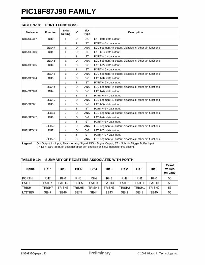
PIC18F87J90 FAMILY
DS39933C-page 130 Preliminary © 2009 Microchip Technology Inc.
TABLE 9-18: PORTH FUNCTIONS
TABLE 9-19: SUMMARY OF REGISTERS ASSOCIATED WITH PORTH
Pin Name Function TRIS Setting I/O I/O
Type Description
RH0/SEG47 RH0 0 O DIG LATH<0> data output.1 I ST PORTH<0> data input.
SEG47 x O ANA LCD segment 47 output; disables all other pin functions.RH1/SEG46 RH1 0 O DIG LATH<1> data output.
1 I ST PORTH<1> data input.SEG46 x O ANA LCD segment 46 output; disables all other pin functions.
RH2/SEG45 RH2 0 O DIG LATH<2> data output.1 I ST PORTH<2> data input.
SEG45 x O ANA LCD segment 45 output; disables all other pin functions.RH3/SEG44 RH3 0 O DIG LATH<3> data output.
1 I ST PORTH<3> data input.SEG44 x O ANA LCD segment 44 output; disables all other pin functions.
RH4/SEG40 RH4 0 O DIG LATH<4> data output.1 I ST PORTH<4> data input.
SEG40 x O ANA LCD segment 40 output; disables all other pin functions.RH5/SEG41 RH5 0 O DIG LATH<5> data output.
1 I ST PORTH<5> data input.SEG41 x O ANA LCD segment 41 output; disables all other pin functions.
RH6/SEG42 RH6 0 O DIG LATH<6> data output.1 I ST PORTH<6> data input.
SEG42 x O ANA LCD segment 42 output; disables all other pin functions.RH7/SEG43 RH7 0 O DIG LATH<7> data output.
1 I ST PORTH<7> data input.SEG43 x O ANA LCD segment 43 output; disables all other pin functions.
Legend: O = Output, I = Input, ANA = Analog Signal, DIG = Digital Output, ST = Schmitt Trigger Buffer Input, x = Don’t care (TRIS bit does not affect port direction or is overridden for this option).
Name Bit 7 Bit 6 Bit 5 Bit 4 Bit 3 Bit 2 Bit 1 Bit 0Reset Values
on page
PORTH RH7 RH6 RH5 RH4 RH3 RH2 RH1 RH0 56LATH LATH7 LATH6 LATH5 LATH4 LATH3 LATH2 LATH1 LATH0 56TRISH TRISH7 TRISH6 TRISH5 TRISH4 TRISH3 TRISH2 TRISH1 TRISH0 56LCDSE5 SE47 SE46 SE45 SE44 SE43 SE42 SE41 SE40 55
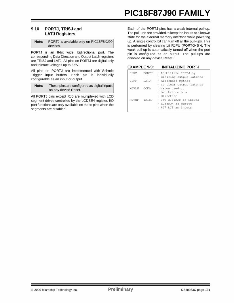
© 2009 Microchip Technology Inc. Preliminary DS39933C-page 131
PIC18F87J90 FAMILY9.10 PORTJ, TRISJ and
LATJ Registers
PORTJ is an 8-bit wide, bidirectional port. Thecorresponding Data Direction and Output Latch registersare TRISJ and LATJ. All pins on PORTJ are digital onlyand tolerate voltages up to 5.5V.
All pins on PORTJ are implemented with SchmittTrigger input buffers. Each pin is individuallyconfigurable as an input or output.
All PORTJ pins except RJ0 are multiplexed with LCDsegment drives controlled by the LCDSE4 register. I/Oport functions are only available on these pins when thesegments are disabled.
Each of the PORTJ pins has a weak internal pull-up.The pull-ups are provided to keep the inputs at a knownstate for the external memory interface while poweringup. A single control bit can turn off all the pull-ups. Thisis performed by clearing bit RJPU (PORTG<5>). Theweak pull-up is automatically turned off when the portpin is configured as an output. The pull-ups aredisabled on any device Reset.
EXAMPLE 9-9: INITIALIZING PORTJ
Note: PORTJ is available only on PIC18F8XJ90devices.
Note: These pins are configured as digital inputson any device Reset.
CLRF PORTJ ; Initialize PORTJ by; clearing output latches
CLRF LATJ ; Alternate method; to clear output latches
MOVLW 0CFh ; Value used to ; initialize data ; direction
MOVWF TRISJ ; Set RJ3:RJ0 as inputs; RJ5:RJ4 as output; RJ7:RJ6 as inputs
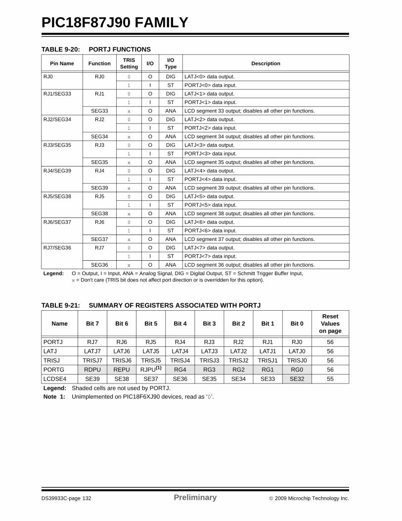
PIC18F87J90 FAMILY
DS39933C-page 132 Preliminary © 2009 Microchip Technology Inc.
TABLE 9-20: PORTJ FUNCTIONS
TABLE 9-21: SUMMARY OF REGISTERS ASSOCIATED WITH PORTJ
Pin Name Function TRIS Setting I/O I/O
Type Description
RJ0 RJ0 0 O DIG LATJ<0> data output.1 I ST PORTJ<0> data input.
RJ1/SEG33 RJ1 0 O DIG LATJ<1> data output.1 I ST PORTJ<1> data input.
SEG33 x O ANA LCD segment 33 output; disables all other pin functions.RJ2/SEG34 RJ2 0 O DIG LATJ<2> data output.
1 I ST PORTJ<2> data input.SEG34 x O ANA LCD segment 34 output; disables all other pin functions.
RJ3/SEG35 RJ3 0 O DIG LATJ<3> data output.1 I ST PORTJ<3> data input.
SEG35 x O ANA LCD segment 35 output; disables all other pin functions.RJ4/SEG39 RJ4 0 O DIG LATJ<4> data output.
1 I ST PORTJ<4> data input.SEG39 x O ANA LCD segment 39 output; disables all other pin functions.
RJ5/SEG38 RJ5 0 O DIG LATJ<5> data output.1 I ST PORTJ<5> data input.
SEG38 x O ANA LCD segment 38 output; disables all other pin functions.RJ6/SEG37 RJ6 0 O DIG LATJ<6> data output.
1 I ST PORTJ<6> data input.SEG37 x O ANA LCD segment 37 output; disables all other pin functions.
RJ7/SEG36 RJ7 0 O DIG LATJ<7> data output.1 I ST PORTJ<7> data input.
SEG36 x O ANA LCD segment 36 output; disables all other pin functions.Legend: O = Output, I = Input, ANA = Analog Signal, DIG = Digital Output, ST = Schmitt Trigger Buffer Input,
x = Don’t care (TRIS bit does not affect port direction or is overridden for this option).
Name Bit 7 Bit 6 Bit 5 Bit 4 Bit 3 Bit 2 Bit 1 Bit 0Reset Values
on page
PORTJ RJ7 RJ6 RJ5 RJ4 RJ3 RJ2 RJ1 RJ0 56LATJ LATJ7 LATJ6 LATJ5 LATJ4 LATJ3 LATJ2 LATJ1 LATJ0 56TRISJ TRISJ7 TRISJ6 TRISJ5 TRISJ4 TRISJ3 TRISJ2 TRISJ1 TRISJ0 56PORTG RDPU REPU RJPU(1) RG4 RG3 RG2 RG1 RG0 56LCDSE4 SE39 SE38 SE37 SE36 SE35 SE34 SE33 SE32 55Legend: Shaded cells are not used by PORTJ.Note 1: Unimplemented on PIC18F6XJ90 devices, read as ‘0’.
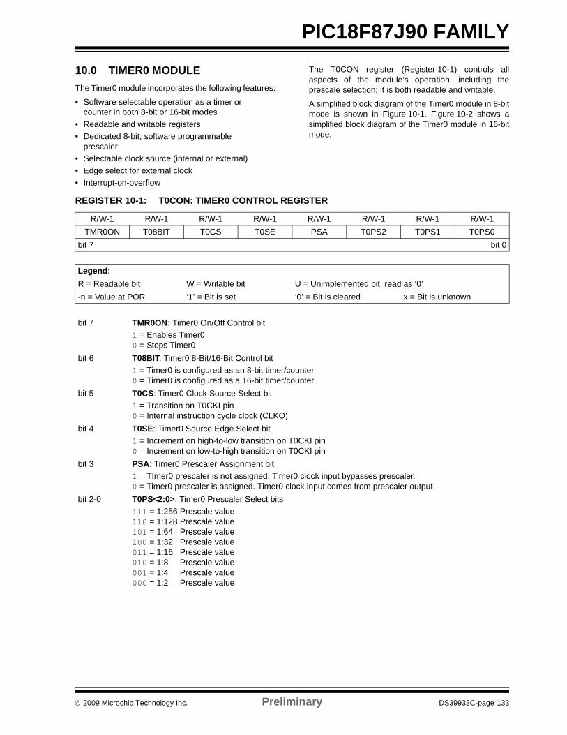
© 2009 Microchip Technology Inc. Preliminary DS39933C-page 133
PIC18F87J90 FAMILY
10.0 TIMER0 MODULEThe Timer0 module incorporates the following features:
• Software selectable operation as a timer or counter in both 8-bit or 16-bit modes
• Readable and writable registers• Dedicated 8-bit, software programmable
prescaler• Selectable clock source (internal or external)• Edge select for external clock• Interrupt-on-overflow
The T0CON register (Register 10-1) controls allaspects of the module’s operation, including theprescale selection; it is both readable and writable.
A simplified block diagram of the Timer0 module in 8-bitmode is shown in Figure 10-1. Figure 10-2 shows asimplified block diagram of the Timer0 module in 16-bitmode.
REGISTER 10-1: T0CON: TIMER0 CONTROL REGISTER
R/W-1 R/W-1 R/W-1 R/W-1 R/W-1 R/W-1 R/W-1 R/W-1TMR0ON T08BIT T0CS T0SE PSA T0PS2 T0PS1 T0PS0
bit 7 bit 0
Legend:R = Readable bit W = Writable bit U = Unimplemented bit, read as ‘0’-n = Value at POR ‘1’ = Bit is set ‘0’ = Bit is cleared x = Bit is unknown
bit 7 TMR0ON: Timer0 On/Off Control bit 1 = Enables Timer0 0 = Stops Timer0
bit 6 T08BIT: Timer0 8-Bit/16-Bit Control bit 1 = Timer0 is configured as an 8-bit timer/counter 0 = Timer0 is configured as a 16-bit timer/counter
bit 5 T0CS: Timer0 Clock Source Select bit 1 = Transition on T0CKI pin 0 = Internal instruction cycle clock (CLKO)
bit 4 T0SE: Timer0 Source Edge Select bit1 = Increment on high-to-low transition on T0CKI pin 0 = Increment on low-to-high transition on T0CKI pin
bit 3 PSA: Timer0 Prescaler Assignment bit 1 = TImer0 prescaler is not assigned. Timer0 clock input bypasses prescaler. 0 = Timer0 prescaler is assigned. Timer0 clock input comes from prescaler output.
bit 2-0 T0PS<2:0>: Timer0 Prescaler Select bits 111 = 1:256 Prescale value110 = 1:128 Prescale value101 = 1:64 Prescale value100 = 1:32 Prescale value011 = 1:16 Prescale value010 = 1:8 Prescale value001 = 1:4 Prescale value000 = 1:2 Prescale value
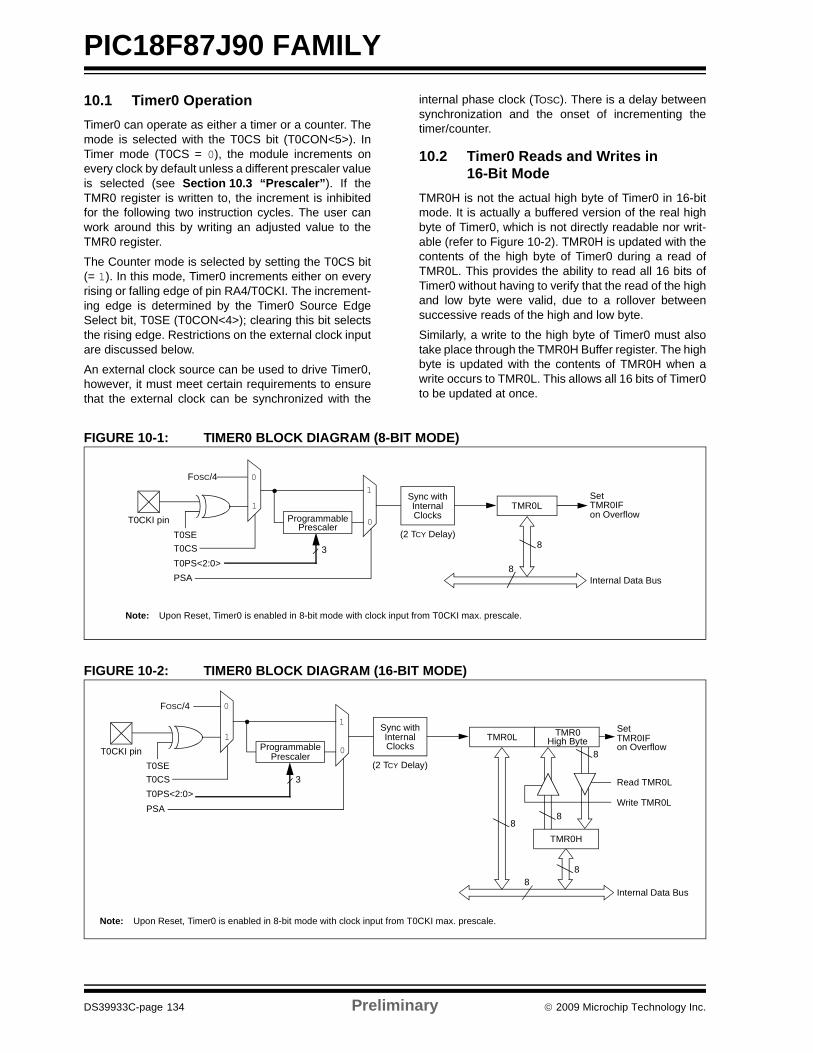
PIC18F87J90 FAMILY
DS39933C-page 134 Preliminary © 2009 Microchip Technology Inc.
10.1 Timer0 OperationTimer0 can operate as either a timer or a counter. Themode is selected with the T0CS bit (T0CON<5>). InTimer mode (T0CS = 0), the module increments onevery clock by default unless a different prescaler valueis selected (see Section 10.3 “Prescaler”). If theTMR0 register is written to, the increment is inhibitedfor the following two instruction cycles. The user canwork around this by writing an adjusted value to theTMR0 register.
The Counter mode is selected by setting the T0CS bit(= 1). In this mode, Timer0 increments either on everyrising or falling edge of pin RA4/T0CKI. The increment-ing edge is determined by the Timer0 Source EdgeSelect bit, T0SE (T0CON<4>); clearing this bit selectsthe rising edge. Restrictions on the external clock inputare discussed below.
An external clock source can be used to drive Timer0,however, it must meet certain requirements to ensurethat the external clock can be synchronized with the
internal phase clock (TOSC). There is a delay betweensynchronization and the onset of incrementing thetimer/counter.
10.2 Timer0 Reads and Writes in 16-Bit Mode
TMR0H is not the actual high byte of Timer0 in 16-bitmode. It is actually a buffered version of the real highbyte of Timer0, which is not directly readable nor writ-able (refer to Figure 10-2). TMR0H is updated with thecontents of the high byte of Timer0 during a read ofTMR0L. This provides the ability to read all 16 bits ofTimer0 without having to verify that the read of the highand low byte were valid, due to a rollover betweensuccessive reads of the high and low byte.
Similarly, a write to the high byte of Timer0 must alsotake place through the TMR0H Buffer register. The highbyte is updated with the contents of TMR0H when awrite occurs to TMR0L. This allows all 16 bits of Timer0to be updated at once.
FIGURE 10-1: TIMER0 BLOCK DIAGRAM (8-BIT MODE)
FIGURE 10-2: TIMER0 BLOCK DIAGRAM (16-BIT MODE)
Note: Upon Reset, Timer0 is enabled in 8-bit mode with clock input from T0CKI max. prescale.
T0CKI pinT0SE
0
1
1
0
T0CS
FOSC/4
Sync withInternalClocks
TMR0L
(2 TCY Delay)
Internal Data BusPSAT0PS<2:0>
Set TMR0IFon Overflow
3 8
8
ProgrammablePrescaler
Note: Upon Reset, Timer0 is enabled in 8-bit mode with clock input from T0CKI max. prescale.
T0CKI pinT0SE
0
1
1
0
T0CS
FOSC/4
Sync withInternalClocks
TMR0L
(2 TCY Delay)
Internal Data Bus
8
PSAT0PS<2:0>
Set TMR0IFon Overflow
3
TMR0
TMR0H
High Byte
88
8
Read TMR0L
Write TMR0L
8
ProgrammablePrescaler
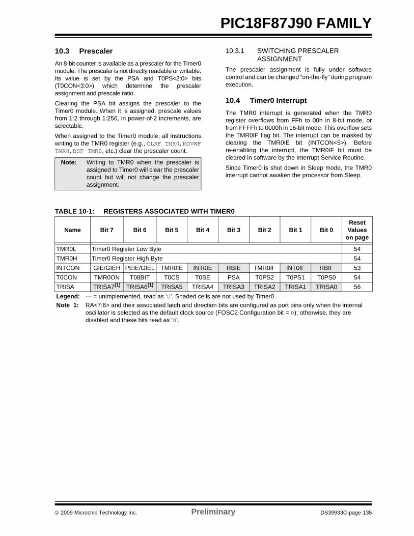
© 2009 Microchip Technology Inc. Preliminary DS39933C-page 135
PIC18F87J90 FAMILY10.3 PrescalerAn 8-bit counter is available as a prescaler for the Timer0module. The prescaler is not directly readable or writable.Its value is set by the PSA and T0PS<2:0> bits(T0CON<3:0>) which determine the prescalerassignment and prescale ratio.
Clearing the PSA bit assigns the prescaler to theTimer0 module. When it is assigned, prescale valuesfrom 1:2 through 1:256, in power-of-2 increments, areselectable.
When assigned to the Timer0 module, all instructionswriting to the TMR0 register (e.g., CLRF TMR0, MOVWFTMR0, BSF TMR0, etc.) clear the prescaler count.
10.3.1 SWITCHING PRESCALER ASSIGNMENT
The prescaler assignment is fully under softwarecontrol and can be changed “on-the-fly” during programexecution.
10.4 Timer0 InterruptThe TMR0 interrupt is generated when the TMR0register overflows from FFh to 00h in 8-bit mode, orfrom FFFFh to 0000h in 16-bit mode. This overflow setsthe TMR0IF flag bit. The interrupt can be masked byclearing the TMR0IE bit (INTCON<5>). Beforere-enabling the interrupt, the TMR0IF bit must becleared in software by the Interrupt Service Routine.
Since Timer0 is shut down in Sleep mode, the TMR0interrupt cannot awaken the processor from Sleep.
TABLE 10-1: REGISTERS ASSOCIATED WITH TIMER0
Note: Writing to TMR0 when the prescaler isassigned to Timer0 will clear the prescalercount but will not change the prescalerassignment.
Name Bit 7 Bit 6 Bit 5 Bit 4 Bit 3 Bit 2 Bit 1 Bit 0Reset Values
on page
TMR0L Timer0 Register Low Byte 54TMR0H Timer0 Register High Byte 54INTCON GIE/GIEH PEIE/GIEL TMR0IE INT0IE RBIE TMR0IF INT0IF RBIF 53T0CON TMR0ON T08BIT T0CS T0SE PSA T0PS2 T0PS1 T0PS0 54TRISA TRISA7(1) TRISA6(1) TRISA5 TRISA4 TRISA3 TRISA2 TRISA1 TRISA0 56Legend: — = unimplemented, read as ‘0’. Shaded cells are not used by Timer0.Note 1: RA<7:6> and their associated latch and direction bits are configured as port pins only when the internal
oscillator is selected as the default clock source (FOSC2 Configuration bit = 0); otherwise, they are disabled and these bits read as ‘0’.

PIC18F87J90 FAMILY
DS39933C-page 136 Preliminary © 2009 Microchip Technology Inc.
NOTES:
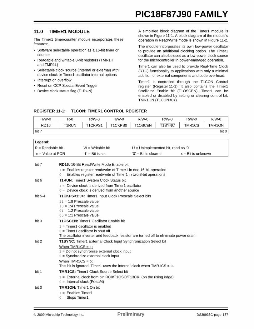
© 2009 Microchip Technology Inc. Preliminary DS39933C-page 137
PIC18F87J90 FAMILY
11.0 TIMER1 MODULEThe Timer1 timer/counter module incorporates thesefeatures:
• Software selectable operation as a 16-bit timer or counter
• Readable and writable 8-bit registers (TMR1H and TMR1L)
• Selectable clock source (internal or external) with device clock or Timer1 oscillator internal options
• Interrupt on overflow• Reset on CCP Special Event Trigger• Device clock status flag (T1RUN)
A simplified block diagram of the Timer1 module isshown in Figure 11-1. A block diagram of the module’soperation in Read/Write mode is shown in Figure 11-2.
The module incorporates its own low-power oscillatorto provide an additional clocking option. The Timer1oscillator can also be used as a low-power clock sourcefor the microcontroller in power-managed operation.
Timer1 can also be used to provide Real-Time Clock(RTC) functionality to applications with only a minimaladdition of external components and code overhead.
Timer1 is controlled through the T1CON Controlregister (Register 11-1). It also contains the Timer1Oscillator Enable bit (T1OSCEN). Timer1 can beenabled or disabled by setting or clearing control bit,TMR1ON (T1CON<0>).
REGISTER 11-1: T1CON: TIMER1 CONTROL REGISTER
R/W-0 R-0 R/W-0 R/W-0 R/W-0 R/W-0 R/W-0 R/W-0
RD16 T1RUN T1CKPS1 T1CKPS0 T1OSCEN T1SYNC TMR1CS TMR1ONbit 7 bit 0
Legend:R = Readable bit W = Writable bit U = Unimplemented bit, read as ‘0’-n = Value at POR ‘1’ = Bit is set ‘0’ = Bit is cleared x = Bit is unknown
bit 7 RD16: 16-Bit Read/Write Mode Enable bit1 = Enables register read/write of TImer1 in one 16-bit operation0 = Enables register read/write of Timer1 in two 8-bit operations
bit 6 T1RUN: Timer1 System Clock Status bit1 = Device clock is derived from Timer1 oscillator0 = Device clock is derived from another source
bit 5-4 T1CKPS<1:0>: Timer1 Input Clock Prescale Select bits11 = 1:8 Prescale value 10 = 1:4 Prescale value 01 = 1:2 Prescale value 00 = 1:1 Prescale value
bit 3 T1OSCEN: Timer1 Oscillator Enable bit1 = Timer1 oscillator is enabled 0 = Timer1 oscillator is shut off The oscillator inverter and feedback resistor are turned off to eliminate power drain.
bit 2 T1SYNC: Timer1 External Clock Input Synchronization Select bitWhen TMR1CS = 1: 1 = Do not synchronize external clock input 0 = Synchronize external clock inputWhen TMR1CS = 0: This bit is ignored. Timer1 uses the internal clock when TMR1CS = 0.
bit 1 TMR1CS: Timer1 Clock Source Select bit1 = External clock from pin RC0/T1OSO/T13CKI (on the rising edge) 0 = Internal clock (FOSC/4)
bit 0 TMR1ON: Timer1 On bit1 = Enables Timer1 0 = Stops Timer1
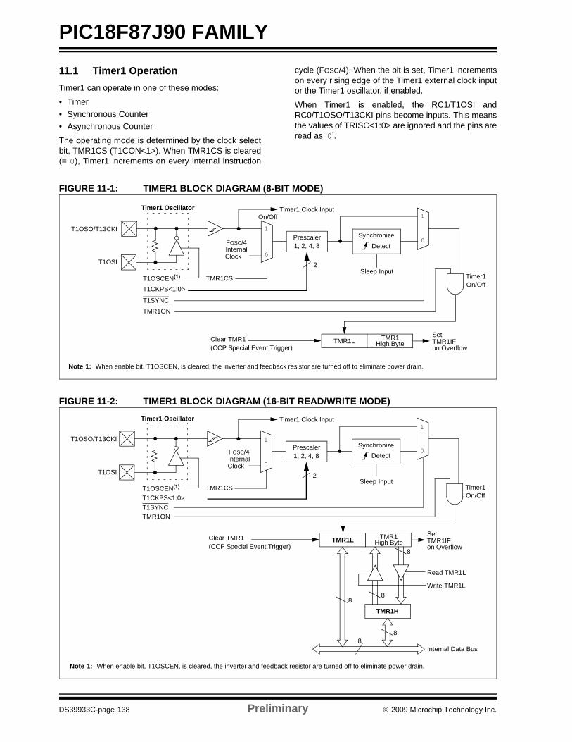
PIC18F87J90 FAMILY
DS39933C-page 138 Preliminary © 2009 Microchip Technology Inc.
11.1 Timer1 OperationTimer1 can operate in one of these modes:
• Timer• Synchronous Counter• Asynchronous Counter
The operating mode is determined by the clock selectbit, TMR1CS (T1CON<1>). When TMR1CS is cleared(= 0), Timer1 increments on every internal instruction
cycle (FOSC/4). When the bit is set, Timer1 incrementson every rising edge of the Timer1 external clock inputor the Timer1 oscillator, if enabled.
When Timer1 is enabled, the RC1/T1OSI andRC0/T1OSO/T13CKI pins become inputs. This meansthe values of TRISC<1:0> are ignored and the pins areread as ‘0’.
FIGURE 11-1: TIMER1 BLOCK DIAGRAM (8-BIT MODE)
FIGURE 11-2: TIMER1 BLOCK DIAGRAM (16-BIT READ/WRITE MODE)
T1SYNC
TMR1CST1CKPS<1:0>
Sleep InputT1OSCEN(1)
FOSC/4InternalClock
On/Off
1
0
2
T1OSO/T13CKI
T1OSI
1
0
TMR1ON
TMR1LSet TMR1IFon Overflow
TMR1High Byte
Clear TMR1(CCP Special Event Trigger)
Timer1 Oscillator
Note 1: When enable bit, T1OSCEN, is cleared, the inverter and feedback resistor are turned off to eliminate power drain.
On/OffTimer1
Timer1 Clock Input
Prescaler1, 2, 4, 8
SynchronizeDetect
T1SYNC
TMR1CST1CKPS<1:0>
Sleep InputT1OSCEN(1)
FOSC/4InternalClock
1
0
2
T1OSO/T13CKI
T1OSI
Note 1: When enable bit, T1OSCEN, is cleared, the inverter and feedback resistor are turned off to eliminate power drain.
1
0
TMR1L
Internal Data Bus
8
Set TMR1IFon Overflow
TMR1
TMR1H
High Byte
88
8
Read TMR1L
Write TMR1L
8
TMR1ON
Clear TMR1(CCP Special Event Trigger)
Timer1 Oscillator
On/OffTimer1
Timer1 Clock Input
Prescaler1, 2, 4, 8
SynchronizeDetect
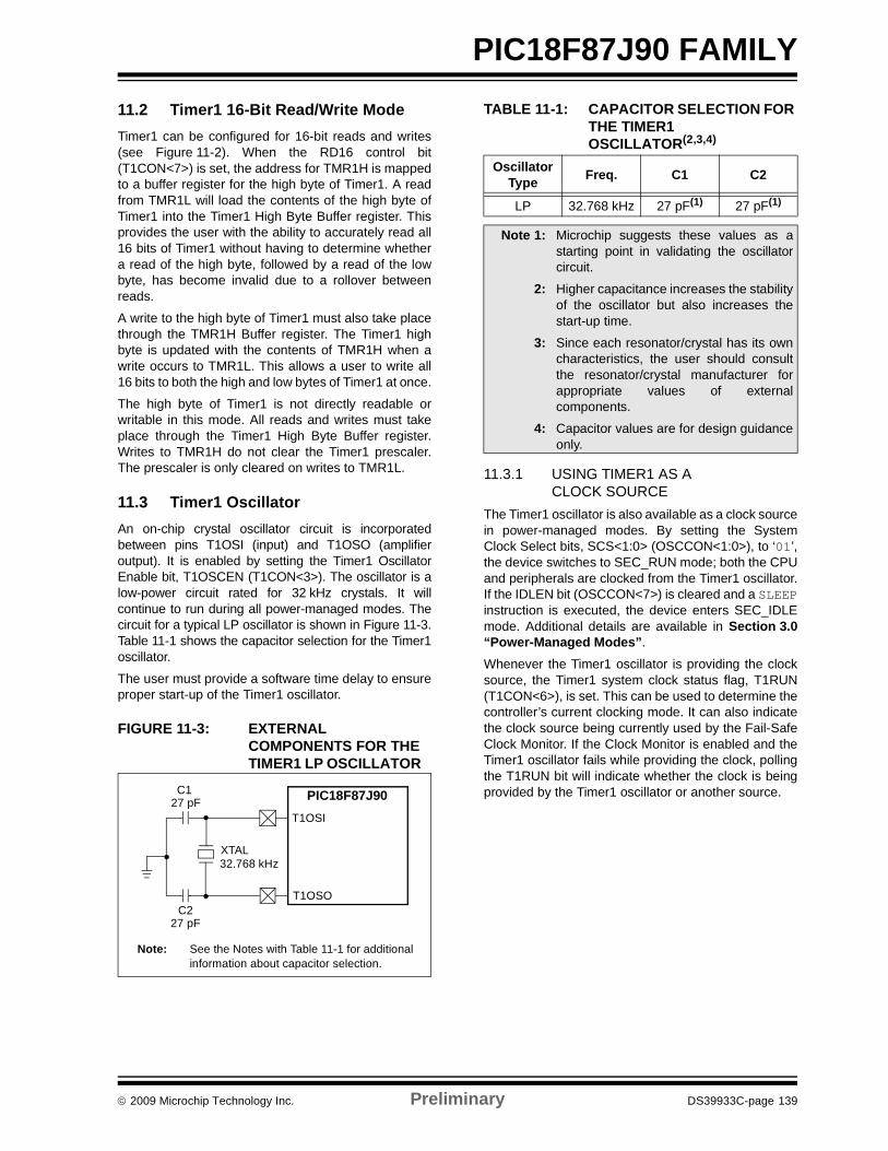
© 2009 Microchip Technology Inc. Preliminary DS39933C-page 139
PIC18F87J90 FAMILY11.2 Timer1 16-Bit Read/Write ModeTimer1 can be configured for 16-bit reads and writes(see Figure 11-2). When the RD16 control bit(T1CON<7>) is set, the address for TMR1H is mappedto a buffer register for the high byte of Timer1. A readfrom TMR1L will load the contents of the high byte ofTimer1 into the Timer1 High Byte Buffer register. Thisprovides the user with the ability to accurately read all16 bits of Timer1 without having to determine whethera read of the high byte, followed by a read of the lowbyte, has become invalid due to a rollover betweenreads.
A write to the high byte of Timer1 must also take placethrough the TMR1H Buffer register. The Timer1 highbyte is updated with the contents of TMR1H when awrite occurs to TMR1L. This allows a user to write all16 bits to both the high and low bytes of Timer1 at once.
The high byte of Timer1 is not directly readable orwritable in this mode. All reads and writes must takeplace through the Timer1 High Byte Buffer register.Writes to TMR1H do not clear the Timer1 prescaler.The prescaler is only cleared on writes to TMR1L.
11.3 Timer1 OscillatorAn on-chip crystal oscillator circuit is incorporatedbetween pins T1OSI (input) and T1OSO (amplifieroutput). It is enabled by setting the Timer1 OscillatorEnable bit, T1OSCEN (T1CON<3>). The oscillator is alow-power circuit rated for 32 kHz crystals. It willcontinue to run during all power-managed modes. Thecircuit for a typical LP oscillator is shown in Figure 11-3.Table 11-1 shows the capacitor selection for the Timer1oscillator.
The user must provide a software time delay to ensureproper start-up of the Timer1 oscillator.
FIGURE 11-3: EXTERNAL COMPONENTS FOR THE TIMER1 LP OSCILLATOR
TABLE 11-1: CAPACITOR SELECTION FOR THE TIMER1 OSCILLATOR(2,3,4)
11.3.1 USING TIMER1 AS A CLOCK SOURCE
The Timer1 oscillator is also available as a clock sourcein power-managed modes. By setting the SystemClock Select bits, SCS<1:0> (OSCCON<1:0>), to ‘01’,the device switches to SEC_RUN mode; both the CPUand peripherals are clocked from the Timer1 oscillator.If the IDLEN bit (OSCCON<7>) is cleared and a SLEEPinstruction is executed, the device enters SEC_IDLEmode. Additional details are available in Section 3.0“Power-Managed Modes”.
Whenever the Timer1 oscillator is providing the clocksource, the Timer1 system clock status flag, T1RUN(T1CON<6>), is set. This can be used to determine thecontroller’s current clocking mode. It can also indicatethe clock source being currently used by the Fail-SafeClock Monitor. If the Clock Monitor is enabled and theTimer1 oscillator fails while providing the clock, pollingthe T1RUN bit will indicate whether the clock is beingprovided by the Timer1 oscillator or another source.
Note: See the Notes with Table 11-1 for additionalinformation about capacitor selection.
C1
C2
XTAL
T1OSI
T1OSO
32.768 kHz
27 pF
27 pF
PIC18F87J90
Oscillator Type Freq. C1 C2
LP 32.768 kHz 27 pF(1) 27 pF(1)
Note 1: Microchip suggests these values as astarting point in validating the oscillatorcircuit.
2: Higher capacitance increases the stabilityof the oscillator but also increases thestart-up time.
3: Since each resonator/crystal has its owncharacteristics, the user should consultthe resonator/crystal manufacturer forappropriate values of externalcomponents.
4: Capacitor values are for design guidanceonly.
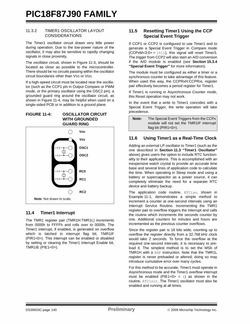
PIC18F87J90 FAMILY
DS39933C-page 140 Preliminary © 2009 Microchip Technology Inc.
11.3.2 TIMER1 OSCILLATOR LAYOUT CONSIDERATIONS
The Timer1 oscillator circuit draws very little powerduring operation. Due to the low-power nature of theoscillator, it may also be sensitive to rapidly changingsignals in close proximity.
The oscillator circuit, shown in Figure 11-3, should belocated as close as possible to the microcontroller.There should be no circuits passing within the oscillatorcircuit boundaries other than VSS or VDD.
If a high-speed circuit must be located near the oscilla-tor (such as the CCP1 pin in Output Compare or PWMmode, or the primary oscillator using the OSC2 pin), agrounded guard ring around the oscillator circuit, asshown in Figure 11-4, may be helpful when used on asingle-sided PCB or in addition to a ground plane.
FIGURE 11-4: OSCILLATOR CIRCUIT WITH GROUNDED GUARD RING
11.4 Timer1 InterruptThe TMR1 register pair (TMR1H:TMR1L) incrementsfrom 0000h to FFFFh and rolls over to 0000h. TheTimer1 interrupt, if enabled, is generated on overflowwhich is latched in interrupt flag bit, TMR1IF(PIR1<0>). This interrupt can be enabled or disabledby setting or clearing the Timer1 Interrupt Enable bit,TMR1IE (PIE1<0>).
11.5 Resetting Timer1 Using the CCP Special Event Trigger
If CCP1 or CCP2 is configured to use Timer1 and togenerate a Special Event Trigger in Compare mode(CCPxM<3:0> = 1011), this signal will reset Timer3.The trigger from CCP2 will also start an A/D conversionif the A/D module is enabled (see Section 15.3.4“Special Event Trigger” for more information).
The module must be configured as either a timer or asynchronous counter to take advantage of this feature.When used this way, the CCPRxH:CCPRxL registerpair effectively becomes a period register for Timer1.
If Timer1 is running in Asynchronous Counter mode,this Reset operation may not work.
In the event that a write to Timer1 coincides with aSpecial Event Trigger, the write operation will takeprecedence.
11.6 Using Timer1 as a Real-Time ClockAdding an external LP oscillator to Timer1 (such as theone described in Section 11.3 “Timer1 Oscillator”above) gives users the option to include RTC function-ality to their applications. This is accomplished with aninexpensive watch crystal to provide an accurate timebase and several lines of application code to calculatethe time. When operating in Sleep mode and using abattery or supercapacitor as a power source, it cancompletely eliminate the need for a separate RTCdevice and battery backup.
The application code routine, RTCisr, shown inExample 11-1, demonstrates a simple method toincrement a counter at one-second intervals using anInterrupt Service Routine. Incrementing the TMR1register pair to overflow triggers the interrupt and callsthe routine which increments the seconds counter byone. Additional counters for minutes and hours areincremented as the previous counter overflows.
Since the register pair is 16 bits wide, counting up tooverflow the register directly from a 32.768 kHz clockwould take 2 seconds. To force the overflow at therequired one-second intervals, it is necessary to pre-load it. The simplest method is to set the MSb ofTMR1H with a BSF instruction. Note that the TMR1Lregister is never preloaded or altered; doing so mayintroduce cumulative error over many cycles.
For this method to be accurate, Timer1 must operate inAsynchronous mode and the Timer1 overflow interruptmust be enabled (PIE1<0> = 1) as shown in theroutine, RTCinit. The Timer1 oscillator must also beenabled and running at all times.
VDD
OSC1
VSS
OSC2
RC0
RC1
RC2
Note: Not drawn to scale.
Note: The Special Event Triggers from the CCPxmodule will not set the TMR1IF interruptflag bit (PIR1<0>).
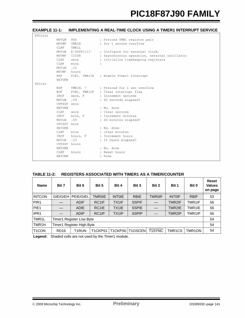
© 2009 Microchip Technology Inc. Preliminary DS39933C-page 141
PIC18F87J90 FAMILYEXAMPLE 11-1: IMPLEMENTING A REAL-TIME CLOCK USING A TIMER1 INTERRUPT SERVICE
TABLE 11-2: REGISTERS ASSOCIATED WITH TIMER1 AS A TIMER/COUNTER
RTCinitMOVLW 80h ; Preload TMR1 register pairMOVWF TMR1H ; for 1 second overflowCLRF TMR1LMOVLW b’00001111’ ; Configure for external clock,MOVWF T1CON ; Asynchronous operation, external oscillatorCLRF secs ; Initialize timekeeping registersCLRF mins ; MOVLW .12MOVWF hoursBSF PIE1, TMR1IE ; Enable Timer1 interruptRETURN
RTCisrBSF TMR1H, 7 ; Preload for 1 sec overflowBCF PIR1, TMR1IF ; Clear interrupt flagINCF secs, F ; Increment secondsMOVLW .59 ; 60 seconds elapsed?CPFSGT secsRETURN ; No, doneCLRF secs ; Clear secondsINCF mins, F ; Increment minutesMOVLW .59 ; 60 minutes elapsed?CPFSGT minsRETURN ; No, doneCLRF mins ; clear minutesINCF hours, F ; Increment hoursMOVLW .23 ; 24 hours elapsed?CPFSGT hoursRETURN ; No, doneCLRF hours ; Reset hoursRETURN ; Done
Name Bit 7 Bit 6 Bit 5 Bit 4 Bit 3 Bit 2 Bit 1 Bit 0Reset Values
on page
INTCON GIE/GIEH PEIE/GIEL TMR0IE INT0IE RBIE TMR0IF INT0IF RBIF 53PIR1 — ADIF RC1IF TX1IF SSPIF — TMR2IF TMR1IF 56PIE1 — ADIE RC1IE TX1IE SSPIE — TMR2IE TMR1IE 56IPR1 — ADIP RC1IP TX1IP SSPIP — TMR2IP TMR1IP 56TMR1L Timer1 Register Low Byte 54TMR1H Timer1 Register High Byte 54
T1CON RD16 T1RUN T1CKPS1 T1CKPS0 T1OSCEN T1SYNC TMR1CS TMR1ON 54
Legend: Shaded cells are not used by the Timer1 module.

PIC18F87J90 FAMILY
DS39933C-page 142 Preliminary © 2009 Microchip Technology Inc.
NOTES:
© 2009 Microchip Technology Inc. Preliminary DS39933C-page 143
PIC18F87J90 FAMILY
12.0 TIMER2 MODULEThe Timer2 module incorporates the following features:
• 8-bit Timer and Period registers (TMR2 and PR2, respectively)
• Readable and writable (both registers) • Software programmable prescaler
(1:1, 1:4 and 1:16)• Software programmable postscaler
(1:1 through 1:16)• Interrupt on TMR2 to PR2 match• Optional use as the shift clock for the
MSSP module
The module is controlled through the T2CON register(Register 12-1) which enables or disables the timer andconfigures the prescaler and postscaler. Timer2 can beshut off by clearing control bit, TMR2ON (T2CON<2>),to minimize power consumption.
A simplified block diagram of the module is shown inFigure 12-1.
12.1 Timer2 OperationIn normal operation, TMR2 is incremented from 00h oneach clock (FOSC/4). A 4-bit counter/prescaler on theclock input gives direct input, divide-by-4 anddivide-by-16 prescale options. These are selected bythe prescaler control bits, T2CKPS<1:0>(T2CON<1:0>). The value of TMR2 is compared to thatof the Period register, PR2, on each clock cycle. Whenthe two values match, the comparator generates amatch signal as the timer output. This signal also resetsthe value of TMR2 to 00h on the next cycle and drivesthe output counter/postscaler (see Section 12.2“Timer2 Interrupt”).
The TMR2 and PR2 registers are both directly readableand writable. The TMR2 register is cleared on anydevice Reset, while the PR2 register initializes at FFh.Both the prescaler and postscaler counters are clearedon the following events:
• a write to the TMR2 register• a write to the T2CON register• any device Reset (Power-on Reset, MCLR Reset,
Watchdog Timer Reset or Brown-out Reset)
TMR2 is not cleared when T2CON is written.
REGISTER 12-1: T2CON: TIMER2 CONTROL REGISTER
U-0 R/W-0 R/W-0 R/W-0 R/W-0 R/W-0 R/W-0 R/W-0— T2OUTPS3 T2OUTPS2 T2OUTPS1 T2OUTPS0 TMR2ON T2CKPS1 T2CKPS0
bit 7 bit 0
Legend:R = Readable bit W = Writable bit U = Unimplemented bit, read as ‘0’-n = Value at POR ‘1’ = Bit is set ‘0’ = Bit is cleared x = Bit is unknown
bit 7 Unimplemented: Read as ‘0’bit 6-3 T2OUTPS<3:0>: Timer2 Output Postscale Select bits
0000 = 1:1 Postscale 0001 = 1:2 Postscale • • • 1111 = 1:16 Postscale
bit 2 TMR2ON: Timer2 On bit1 = Timer2 is on 0 = Timer2 is off
bit 1-0 T2CKPS<1:0>: Timer2 Clock Prescale Select bits00 = Prescaler is 1 01 = Prescaler is 4 1x = Prescaler is 16
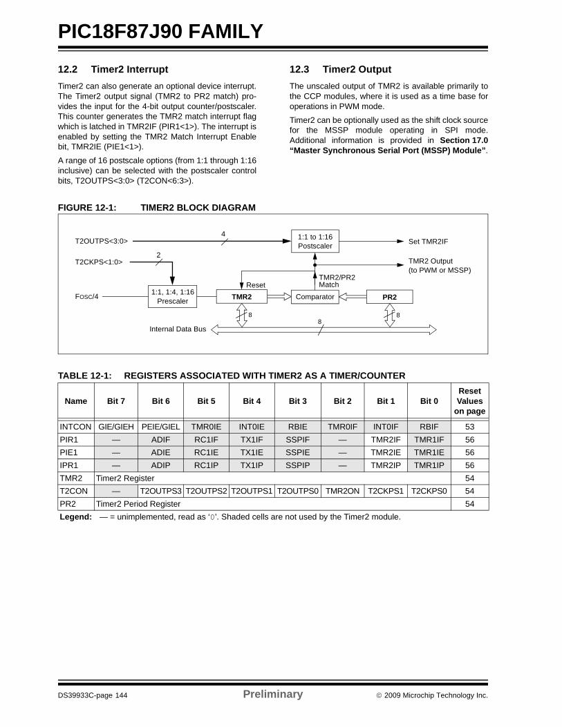
PIC18F87J90 FAMILY
DS39933C-page 144 Preliminary © 2009 Microchip Technology Inc.
12.2 Timer2 InterruptTimer2 can also generate an optional device interrupt.The Timer2 output signal (TMR2 to PR2 match) pro-vides the input for the 4-bit output counter/postscaler.This counter generates the TMR2 match interrupt flagwhich is latched in TMR2IF (PIR1<1>). The interrupt isenabled by setting the TMR2 Match Interrupt Enablebit, TMR2IE (PIE1<1>).
A range of 16 postscale options (from 1:1 through 1:16inclusive) can be selected with the postscaler controlbits, T2OUTPS<3:0> (T2CON<6:3>).
12.3 Timer2 OutputThe unscaled output of TMR2 is available primarily tothe CCP modules, where it is used as a time base foroperations in PWM mode.
Timer2 can be optionally used as the shift clock sourcefor the MSSP module operating in SPI mode.Additional information is provided in Section 17.0“Master Synchronous Serial Port (MSSP) Module”.
FIGURE 12-1: TIMER2 BLOCK DIAGRAM
TABLE 12-1: REGISTERS ASSOCIATED WITH TIMER2 AS A TIMER/COUNTER
Name Bit 7 Bit 6 Bit 5 Bit 4 Bit 3 Bit 2 Bit 1 Bit 0Reset Values
on page
INTCON GIE/GIEH PEIE/GIEL TMR0IE INT0IE RBIE TMR0IF INT0IF RBIF 53PIR1 — ADIF RC1IF TX1IF SSPIF — TMR2IF TMR1IF 56PIE1 — ADIE RC1IE TX1IE SSPIE — TMR2IE TMR1IE 56IPR1 — ADIP RC1IP TX1IP SSPIP — TMR2IP TMR1IP 56TMR2 Timer2 Register 54T2CON — T2OUTPS3 T2OUTPS2 T2OUTPS1 T2OUTPS0 TMR2ON T2CKPS1 T2CKPS0 54PR2 Timer2 Period Register 54Legend: — = unimplemented, read as ‘0’. Shaded cells are not used by the Timer2 module.
Comparator
TMR2 Output
TMR2
Postscaler
Prescaler PR2
2
FOSC/4
1:1 to 1:16
1:1, 1:4, 1:16
4T2OUTPS<3:0>
T2CKPS<1:0>
Set TMR2IF
Internal Data Bus8
ResetTMR2/PR2
88
(to PWM or MSSP)
Match
© 2009 Microchip Technology Inc. Preliminary DS39933C-page 145
PIC18F87J90 FAMILY
13.0 TIMER3 MODULEThe Timer3 timer/counter module incorporates thesefeatures:
• Software selectable operation as a 16-bit timer or counter
• Readable and writable 8-bit registers (TMR3H and TMR3L)
• Selectable clock source (internal or external) with device clock or Timer1 oscillator internal options
• Interrupt on overflow• Module Reset on CCP Special Event Trigger
A simplified block diagram of the Timer3 module isshown in Figure 13-1. A block diagram of the module’soperation in Read/Write mode is shown in Figure 13-2.
The Timer3 module is controlled through the T3CONregister (Register 13-1). It also selects the clock sourceoptions for the CCP modules. See Section 15.2.2“Timer1/Timer3 Mode Selection” for moreinformation.
REGISTER 13-1: T3CON: TIMER3 CONTROL REGISTER
R/W-0 R/W-0 R/W-0 R/W-0 R/W-0 R/W-0 R/W-0 R/W-0
RD16 T3CCP2 T3CKPS1 T3CKPS0 T3CCP1 T3SYNC TMR3CS TMR3ONbit 7 bit 0
Legend:R = Readable bit W = Writable bit U = Unimplemented bit, read as ‘0’-n = Value at POR ‘1’ = Bit is set ‘0’ = Bit is cleared x = Bit is unknown
bit 7 RD16: 16-Bit Read/Write Mode Enable bit1 = Enables register read/write of Timer3 in one 16-bit operation0 = Enables register read/write of Timer3 in two 8-bit operations
bit 6,3 T3CCP<2:1>: Timer3 and Timer1 to CCPx Enable bits1x = Timer3 is the capture/compare clock source for the CCP modules01 = Timer3 is the capture/compare clock source for CCP2;
Timer1 is the capture/compare clock source for CCP100 = Timer1 is the capture/compare clock source for the CCP modules
bit 5-4 T3CKPS<1:0>: Timer3 Input Clock Prescale Select bits11 = 1:8 Prescale value10 = 1:4 Prescale value01 = 1:2 Prescale value00 = 1:1 Prescale value
bit 2 T3SYNC: Timer3 External Clock Input Synchronization Control bit (Not usable if the device clock comes from Timer1/Timer3.)When TMR3CS = 1:1 = Do not synchronize external clock input0 = Synchronize external clock inputWhen TMR3CS = 0:This bit is ignored. Timer3 uses the internal clock when TMR3CS = 0.
bit 1 TMR3CS: Timer3 Clock Source Select bit1 = External clock input from Timer1 oscillator or T13CKI (on the rising edge after the first
falling edge)0 = Internal clock (FOSC/4)
bit 0 TMR3ON: Timer3 On bit1 = Enables Timer3 0 = Stops Timer3
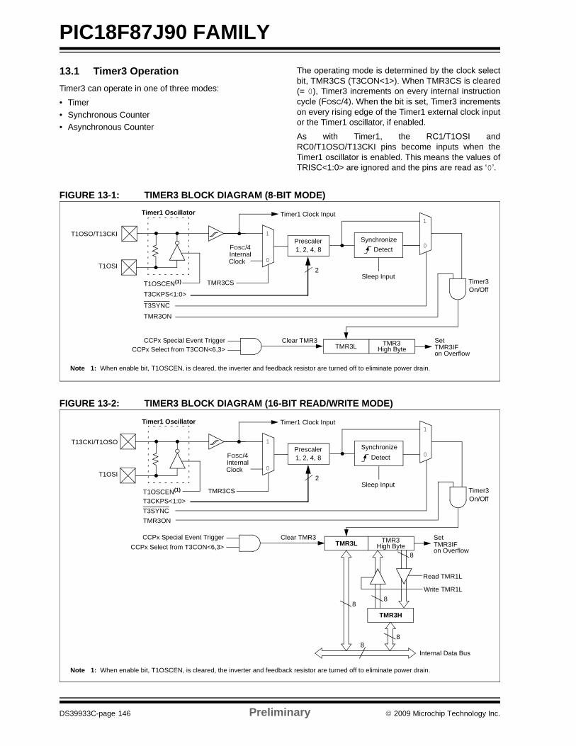
PIC18F87J90 FAMILY
DS39933C-page 146 Preliminary © 2009 Microchip Technology Inc.
13.1 Timer3 OperationTimer3 can operate in one of three modes:
• Timer• Synchronous Counter• Asynchronous Counter
The operating mode is determined by the clock selectbit, TMR3CS (T3CON<1>). When TMR3CS is cleared(= 0), Timer3 increments on every internal instructioncycle (FOSC/4). When the bit is set, Timer3 incrementson every rising edge of the Timer1 external clock inputor the Timer1 oscillator, if enabled.
As with Timer1, the RC1/T1OSI andRC0/T1OSO/T13CKI pins become inputs when theTimer1 oscillator is enabled. This means the values ofTRISC<1:0> are ignored and the pins are read as ‘0’.
FIGURE 13-1: TIMER3 BLOCK DIAGRAM (8-BIT MODE)
FIGURE 13-2: TIMER3 BLOCK DIAGRAM (16-BIT READ/WRITE MODE)
T3SYNC
TMR3CS
T3CKPS<1:0>
Sleep InputT1OSCEN(1)
FOSC/4InternalClock
Prescaler1, 2, 4, 8
SynchronizeDetect
1
0
2
T1OSO/T13CKI
T1OSI
1
0
TMR3ON
TMR3LSet TMR3IFon Overflow
TMR3High Byte
Timer1 Oscillator
Note 1: When enable bit, T1OSCEN, is cleared, the inverter and feedback resistor are turned off to eliminate power drain.
On/OffTimer3
CCPx Special Event TriggerCCPx Select from T3CON<6,3>
Clear TMR3
Timer1 Clock Input
T3SYNC
TMR3CST3CKPS<1:0>
Sleep InputT1OSCEN(1)
FOSC/4InternalClock
Prescaler1, 2, 4, 8
SynchronizeDetect
1
0
2
T13CKI/T1OSO
T1OSI
Note 1: When enable bit, T1OSCEN, is cleared, the inverter and feedback resistor are turned off to eliminate power drain.
1
0
TMR3L
Internal Data Bus
8
Set TMR3IFon Overflow
TMR3
TMR3H
High Byte
88
8
Read TMR1L
Write TMR1L
8
TMR3ON
CCPx Special Event Trigger
Timer1 Oscillator
On/OffTimer3
Timer1 Clock Input
CCPx Select from T3CON<6,3>Clear TMR3
© 2009 Microchip Technology Inc. Preliminary DS39933C-page 147
PIC18F87J90 FAMILY13.2 Timer3 16-Bit Read/Write ModeTimer3 can be configured for 16-bit reads and writes(see Figure 13-2). When the RD16 control bit(T3CON<7>) is set, the address for TMR3H is mappedto a buffer register for the high byte of Timer3. A readfrom TMR3L will load the contents of the high byte ofTimer3 into the Timer3 High Byte Buffer register. Thisprovides the user with the ability to accurately read all16 bits of Timer1 without having to determine whethera read of the high byte, followed by a read of the lowbyte, has become invalid due to a rollover betweenreads.
A write to the high byte of Timer3 must also take placethrough the TMR3H Buffer register. The Timer3 highbyte is updated with the contents of TMR3H when awrite occurs to TMR3L. This allows a user to write all16 bits to both the high and low bytes of Timer3 at once.
The high byte of Timer3 is not directly readable orwritable in this mode. All reads and writes must takeplace through the Timer3 High Byte Buffer register.
Writes to TMR3H do not clear the Timer3 prescaler.The prescaler is only cleared on writes to TMR3L.
13.3 Using the Timer1 Oscillator as the Timer3 Clock Source
The Timer1 internal oscillator may be used as the clocksource for Timer3. The Timer1 oscillator is enabled bysetting the T1OSCEN (T1CON<3>) bit. To use it as theTimer3 clock source, the TMR3CS bit must also be set.As previously noted, this also configures Timer3 toincrement on every rising edge of the oscillator source.
The Timer1 oscillator is described in Section 11.0“Timer1 Module”.
13.4 Timer3 InterruptThe TMR3 register pair (TMR3H:TMR3L) incrementsfrom 0000h to FFFFh and overflows to 0000h. TheTimer3 interrupt, if enabled, is generated on overflowand is latched in interrupt flag bit, TMR3IF (PIR2<1>).This interrupt can be enabled or disabled by setting orclearing the Timer3 Interrupt Enable bit, TMR3IE(PIE2<1>).
13.5 Resetting Timer3 Using the CCP Special Event Trigger
If CCP1 or CCP2 is configured to use Timer3 and togenerate a Special Event Trigger in Compare mode(CCPxM<3:0> = 1011), this signal will reset Timer3.The trigger from CCP2 will also start an A/D conversionif the A/D module is enabled (see Section 15.3.4“Special Event Trigger” for more information).
The module must be configured as either a timer orsynchronous counter to take advantage of this feature.When used this way, the CCPRxH:CCPRxL registerpair effectively becomes a period register for Timer3.
If Timer3 is running in Asynchronous Counter mode,the Reset operation may not work.
In the event that a write to Timer3 coincides with aSpecial Event Trigger from a CCP module, the write willtake precedence.
TABLE 13-1: REGISTERS ASSOCIATED WITH TIMER3 AS A TIMER/COUNTER
Note: The Special Event Triggers from the CCPxmodule will not set the TMR3IF interruptflag bit (PIR2<1>).
Name Bit 7 Bit 6 Bit 5 Bit 4 Bit 3 Bit 2 Bit 1 Bit 0Reset Values
on page
INTCON GIE/GIEH PEIE/GIEL TMR0IE INT0IE RBIE TMR0IF INT0IF RBIF 53PIR2 OSCFIF CMIF — — BCLIF LVDIF TMR3IF — 56PIE2 OSCFIE CMIE — — BCLIE LVDIE TMR3IE — 56IPR2 OSCFIP CMIP — — BCLIP LVDIP TMR3IP — 56TMR3L Timer3 Register Low Byte 55TMR3H Timer3 Register High Byte 55
T1CON RD16 T1RUN T1CKPS1 T1CKPS0 T1OSCEN T1SYNC TMR1CS TMR1ON 54
T3CON RD16 T3CCP2 T3CKPS1 T3CKPS0 T3CCP1 T3SYNC TMR3CS TMR3ON 55
Legend: — = unimplemented, read as ‘0’. Shaded cells are not used by the Timer3 module.

PIC18F87J90 FAMILY
DS39933C-page 148 Preliminary © 2009 Microchip Technology Inc.
NOTES:
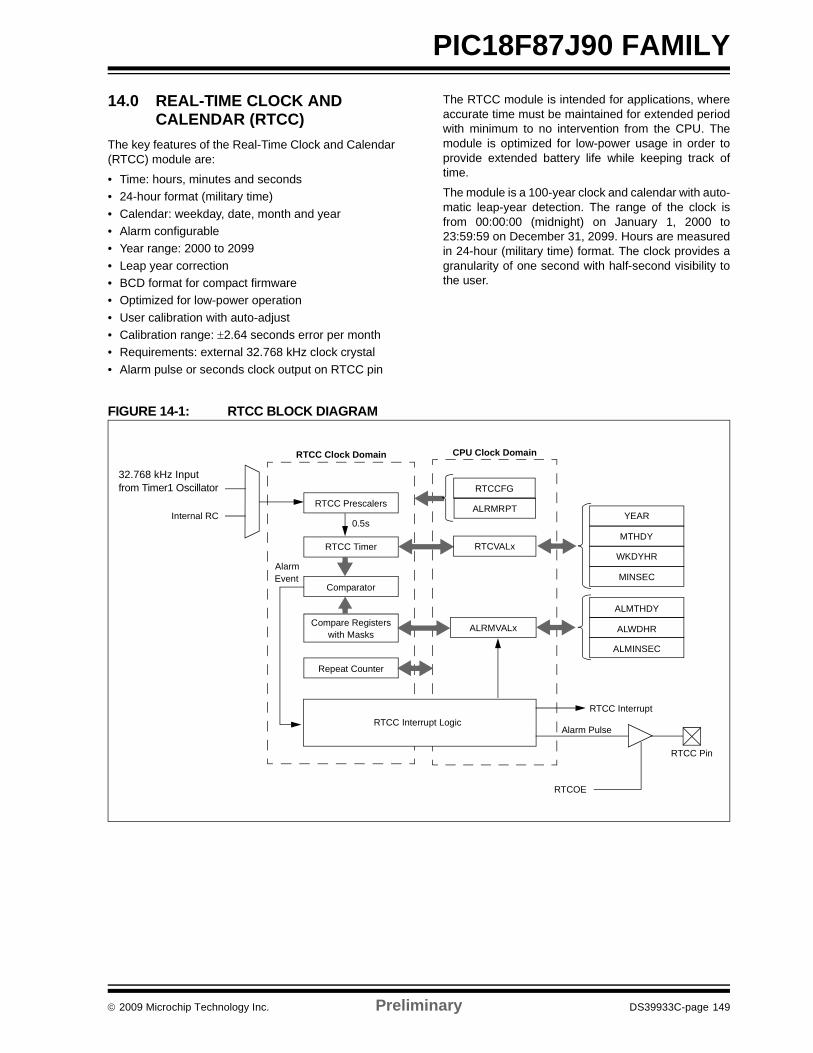
© 2009 Microchip Technology Inc. Preliminary DS39933C-page 149
PIC18F87J90 FAMILY
14.0 REAL-TIME CLOCK AND CALENDAR (RTCC)
The key features of the Real-Time Clock and Calendar(RTCC) module are:
• Time: hours, minutes and seconds• 24-hour format (military time)• Calendar: weekday, date, month and year• Alarm configurable• Year range: 2000 to 2099• Leap year correction• BCD format for compact firmware• Optimized for low-power operation• User calibration with auto-adjust• Calibration range: ±2.64 seconds error per month• Requirements: external 32.768 kHz clock crystal• Alarm pulse or seconds clock output on RTCC pin
The RTCC module is intended for applications, whereaccurate time must be maintained for extended periodwith minimum to no intervention from the CPU. Themodule is optimized for low-power usage in order toprovide extended battery life while keeping track oftime.
The module is a 100-year clock and calendar with auto-matic leap-year detection. The range of the clock isfrom 00:00:00 (midnight) on January 1, 2000 to23:59:59 on December 31, 2099. Hours are measuredin 24-hour (military time) format. The clock provides agranularity of one second with half-second visibility tothe user.
FIGURE 14-1: RTCC BLOCK DIAGRAM
RTCC Prescalers
RTCC Timer
Comparator
Compare Registers
Repeat Counter
YEAR
MTHDY
WKDYHR
MINSEC
ALMTHDY
ALWDHR
ALMINSECwith Masks
RTCC Interrupt Logic
RTCCFG
ALRMRPT
AlarmEvent
0.5s
RTCC Clock Domain
Alarm Pulse
RTCC Interrupt
CPU Clock Domain
RTCVALx
ALRMVALx
RTCC Pin
RTCOE
32.768 kHz Inputfrom Timer1 Oscillator
Internal RC
PIC18F87J90 FAMILY
DS39933C-page 150 Preliminary © 2009 Microchip Technology Inc.
14.1 RTCC MODULE REGISTERSThe RTCC module registers are divided into followingcategories:
RTCC Control Registers• RTCCFG• RTCCAL• PADCFG1• ALRMCFG• ALRMRPT
RTCC Value Registers• RTCVALH and RTCVALL – Can access the fol-
lowing registers- YEAR- MONTH- DAY- WEEKDAY- HOUR- MINUTE- SECOND
Alarm Value Registers• ALRMVALH and ALRMVALL – Can access the
following registers:- ALRMMNTH- ALRMDAY- ALRMWD- ALRMHR- ALRMMIN- ALRMSEC
Note: The RTCVALH and RTCVALL registerscan be accessed through RTCRPT<1:0>.ALRMVALH and ALRMVALL can beaccessed through ALRMPTR<1:0>.
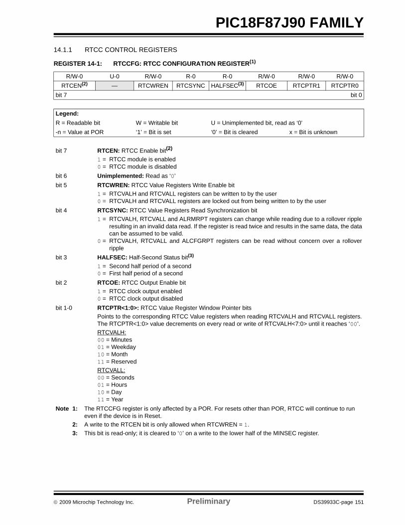
© 2009 Microchip Technology Inc. Preliminary DS39933C-page 151
PIC18F87J90 FAMILY14.1.1 RTCC CONTROL REGISTERS
REGISTER 14-1: RTCCFG: RTCC CONFIGURATION REGISTER(1)
R/W-0 U-0 R/W-0 R-0 R-0 R/W-0 R/W-0 R/W-0RTCEN(2) — RTCWREN RTCSYNC HALFSEC(3) RTCOE RTCPTR1 RTCPTR0
bit 7 bit 0
Legend:R = Readable bit W = Writable bit U = Unimplemented bit, read as ‘0’-n = Value at POR ‘1’ = Bit is set ‘0’ = Bit is cleared x = Bit is unknown
bit 7 RTCEN: RTCC Enable bit(2)
1 = RTCC module is enabled0 = RTCC module is disabled
bit 6 Unimplemented: Read as ‘0’bit 5 RTCWREN: RTCC Value Registers Write Enable bit
1 = RTCVALH and RTCVALL registers can be written to by the user0 = RTCVALH and RTCVALL registers are locked out from being written to by the user
bit 4 RTCSYNC: RTCC Value Registers Read Synchronization bit1 = RTCVALH, RTCVALL and ALRMRPT registers can change while reading due to a rollover ripple
resulting in an invalid data read. If the register is read twice and results in the same data, the datacan be assumed to be valid.
0 = RTCVALH, RTCVALL and ALCFGRPT registers can be read without concern over a rolloverripple
bit 3 HALFSEC: Half-Second Status bit(3)
1 = Second half period of a second0 = First half period of a second
bit 2 RTCOE: RTCC Output Enable bit1 = RTCC clock output enabled0 = RTCC clock output disabled
bit 1-0 RTCPTR<1:0>: RTCC Value Register Window Pointer bitsPoints to the corresponding RTCC Value registers when reading RTCVALH and RTCVALL registers.The RTCPTR<1:0> value decrements on every read or write of RTCVALH<7:0> until it reaches ‘00’.RTCVALH:00 = Minutes01 = Weekday10 = Month11 = ReservedRTCVALL:00 = Seconds01 = Hours10 = Day11 = Year
Note 1: The RTCCFG register is only affected by a POR. For resets other than POR, RTCC will continue to run even if the device is in Reset.
2: A write to the RTCEN bit is only allowed when RTCWREN = 1.3: This bit is read-only; it is cleared to ‘0’ on a write to the lower half of the MINSEC register.
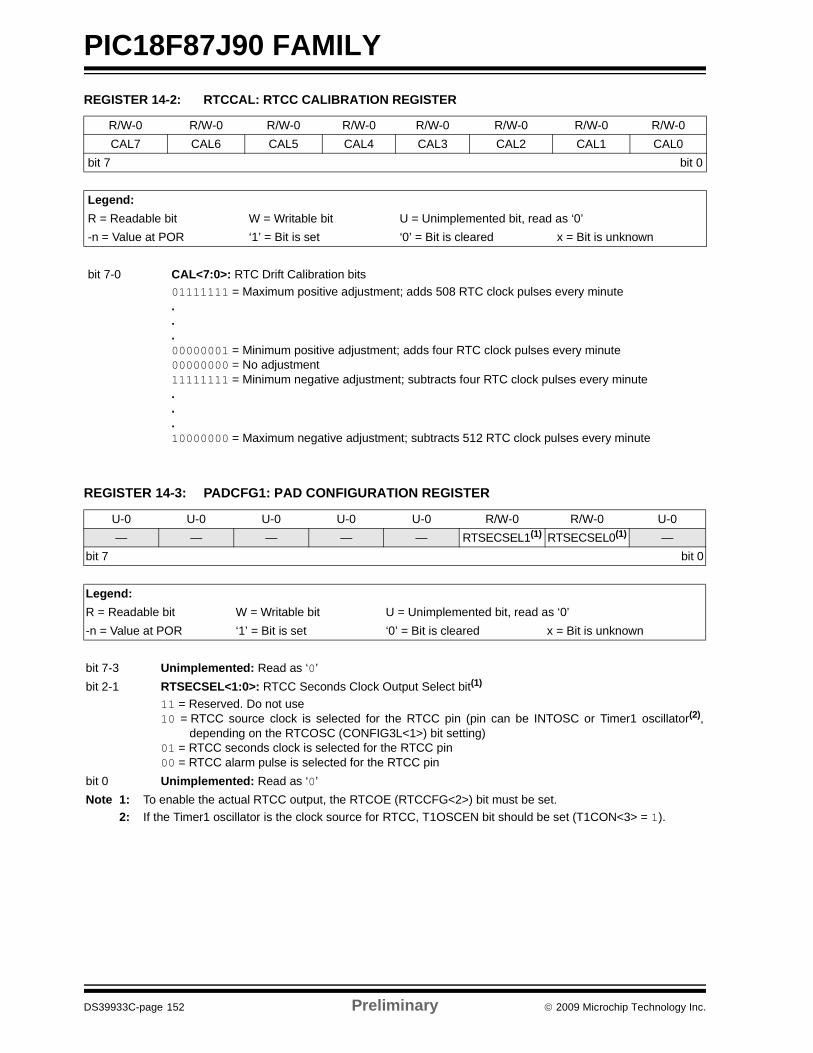
PIC18F87J90 FAMILY
DS39933C-page 152 Preliminary © 2009 Microchip Technology Inc.
REGISTER 14-2: RTCCAL: RTCC CALIBRATION REGISTER
R/W-0 R/W-0 R/W-0 R/W-0 R/W-0 R/W-0 R/W-0 R/W-0CAL7 CAL6 CAL5 CAL4 CAL3 CAL2 CAL1 CAL0
bit 7 bit 0
Legend:R = Readable bit W = Writable bit U = Unimplemented bit, read as ‘0’-n = Value at POR ‘1’ = Bit is set ‘0’ = Bit is cleared x = Bit is unknown
bit 7-0 CAL<7:0>: RTC Drift Calibration bits01111111 = Maximum positive adjustment; adds 508 RTC clock pulses every minute...00000001 = Minimum positive adjustment; adds four RTC clock pulses every minute00000000 = No adjustment11111111 = Minimum negative adjustment; subtracts four RTC clock pulses every minute...10000000 = Maximum negative adjustment; subtracts 512 RTC clock pulses every minute
REGISTER 14-3: PADCFG1: PAD CONFIGURATION REGISTER
U-0 U-0 U-0 U-0 U-0 R/W-0 R/W-0 U-0— — — — — RTSECSEL1(1) RTSECSEL0(1) —
bit 7 bit 0
Legend:R = Readable bit W = Writable bit U = Unimplemented bit, read as ‘0’-n = Value at POR ‘1’ = Bit is set ‘0’ = Bit is cleared x = Bit is unknown
bit 7-3 Unimplemented: Read as ‘0’bit 2-1 RTSECSEL<1:0>: RTCC Seconds Clock Output Select bit(1)
11 = Reserved. Do not use10 = RTCC source clock is selected for the RTCC pin (pin can be INTOSC or Timer1 oscillator(2),
depending on the RTCOSC (CONFIG3L<1>) bit setting)01 = RTCC seconds clock is selected for the RTCC pin00 = RTCC alarm pulse is selected for the RTCC pin
bit 0 Unimplemented: Read as ‘0’Note 1: To enable the actual RTCC output, the RTCOE (RTCCFG<2>) bit must be set.
2: If the Timer1 oscillator is the clock source for RTCC, T1OSCEN bit should be set (T1CON<3> = 1).
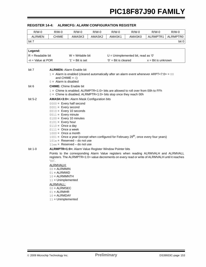
© 2009 Microchip Technology Inc. Preliminary DS39933C-page 153
PIC18F87J90 FAMILYREGISTER 14-4: ALRMCFG: ALARM CONFIGURATION REGISTER
R/W-0 R/W-0 R/W-0 R/W-0 R/W-0 R/W-0 R/W-0 R/W-0ALRMEN CHIME AMASK3 AMASK2 AMASK1 AMASK0 ALRMPTR1 ALRMPTR0
bit 7 bit 0
Legend:R = Readable bit W = Writable bit U = Unimplemented bit, read as ‘0’-n = Value at POR ‘1’ = Bit is set ‘0’ = Bit is cleared x = Bit is unknown
bit 7 ALRMEN: Alarm Enable bit1 = Alarm is enabled (cleared automatically after an alarm event whenever ARPT<7:0> = 00
and CHIME = 0)0 = Alarm is disabled
bit 6 CHIME: Chime Enable bit1 = Chime is enabled; ALRMPTR<1:0> bits are allowed to roll over from 00h to FFh0 = Chime is disabled; ALRMPTR<1:0> bits stop once they reach 00h
bit 5-2 AMASK<3:0>: Alarm Mask Configuration bits0000 = Every half second0001 = Every second0010 = Every 10 seconds0011 = Every minute0100 = Every 10 minutes0101 = Every hour0110 = Once a day0111 = Once a week1000 = Once a month1001 = Once a year (except when configured for February 29th, once every four years)101x = Reserved – do not use11xx = Reserved – do not use
bit 1-0 ALRMPTR<1:0>: Alarm Value Register Window Pointer bitsPoints to the corresponding Alarm Value registers when reading ALRMVALH and ALRMVALLregisters. The ALRMPTR<1:0> value decrements on every read or write of ALRMVALH until it reaches‘00’.ALRMVALH:00 = ALRMMIN01 = ALRMWD10 = ALRMMNTH11 = UnimplementedALRMVALL:00 = ALRMSEC01 = ALRMHR10 = ALRMDAY11 = Unimplemented
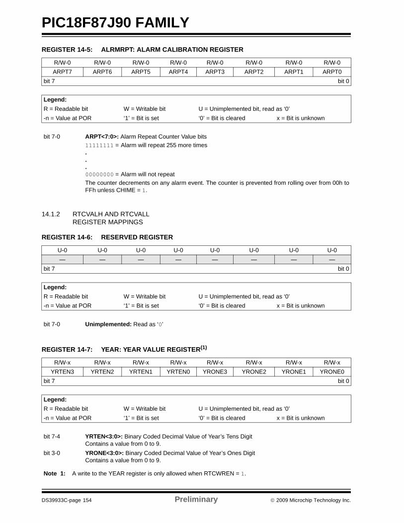
PIC18F87J90 FAMILY
DS39933C-page 154 Preliminary © 2009 Microchip Technology Inc.
14.1.2 RTCVALH AND RTCVALL REGISTER MAPPINGS
REGISTER 14-5: ALRMRPT: ALARM CALIBRATION REGISTER
R/W-0 R/W-0 R/W-0 R/W-0 R/W-0 R/W-0 R/W-0 R/W-0ARPT7 ARPT6 ARPT5 ARPT4 ARPT3 ARPT2 ARPT1 ARPT0
bit 7 bit 0
Legend:R = Readable bit W = Writable bit U = Unimplemented bit, read as ‘0’-n = Value at POR ‘1’ = Bit is set ‘0’ = Bit is cleared x = Bit is unknown
bit 7-0 ARPT<7:0>: Alarm Repeat Counter Value bits11111111 = Alarm will repeat 255 more times...00000000 = Alarm will not repeatThe counter decrements on any alarm event. The counter is prevented from rolling over from 00h toFFh unless CHIME = 1.
REGISTER 14-6: RESERVED REGISTER
U-0 U-0 U-0 U-0 U-0 U-0 U-0 U-0— — — — — — — —
bit 7 bit 0
Legend:R = Readable bit W = Writable bit U = Unimplemented bit, read as ‘0’-n = Value at POR ‘1’ = Bit is set ‘0’ = Bit is cleared x = Bit is unknown
bit 7-0 Unimplemented: Read as ‘0’
REGISTER 14-7: YEAR: YEAR VALUE REGISTER(1)
R/W-x R/W-x R/W-x R/W-x R/W-x R/W-x R/W-x R/W-xYRTEN3 YRTEN2 YRTEN1 YRTEN0 YRONE3 YRONE2 YRONE1 YRONE0
bit 7 bit 0
Legend:R = Readable bit W = Writable bit U = Unimplemented bit, read as ‘0’-n = Value at POR ‘1’ = Bit is set ‘0’ = Bit is cleared x = Bit is unknown
bit 7-4 YRTEN<3:0>: Binary Coded Decimal Value of Year’s Tens DigitContains a value from 0 to 9.
bit 3-0 YRONE<3:0>: Binary Coded Decimal Value of Year’s Ones DigitContains a value from 0 to 9.
Note 1: A write to the YEAR register is only allowed when RTCWREN = 1.
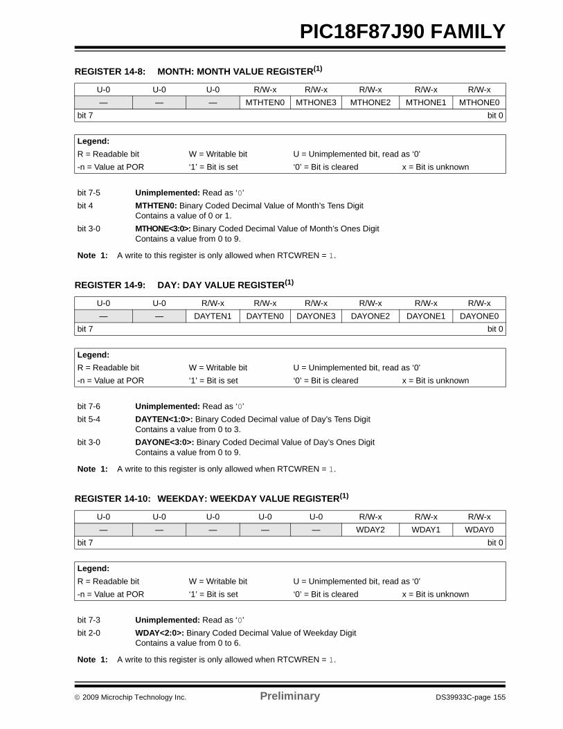
© 2009 Microchip Technology Inc. Preliminary DS39933C-page 155
PIC18F87J90 FAMILY
REGISTER 14-8: MONTH: MONTH VALUE REGISTER(1)
U-0 U-0 U-0 R/W-x R/W-x R/W-x R/W-x R/W-x— — — MTHTEN0 MTHONE3 MTHONE2 MTHONE1 MTHONE0
bit 7 bit 0
Legend:R = Readable bit W = Writable bit U = Unimplemented bit, read as ‘0’-n = Value at POR ‘1’ = Bit is set ‘0’ = Bit is cleared x = Bit is unknown
bit 7-5 Unimplemented: Read as ‘0’bit 4 MTHTEN0: Binary Coded Decimal Value of Month’s Tens Digit
Contains a value of 0 or 1.bit 3-0 MTHONE<3:0>: Binary Coded Decimal Value of Month’s Ones Digit
Contains a value from 0 to 9.
Note 1: A write to this register is only allowed when RTCWREN = 1.
REGISTER 14-9: DAY: DAY VALUE REGISTER(1)
U-0 U-0 R/W-x R/W-x R/W-x R/W-x R/W-x R/W-x— — DAYTEN1 DAYTEN0 DAYONE3 DAYONE2 DAYONE1 DAYONE0
bit 7 bit 0
Legend:R = Readable bit W = Writable bit U = Unimplemented bit, read as ‘0’-n = Value at POR ‘1’ = Bit is set ‘0’ = Bit is cleared x = Bit is unknown
bit 7-6 Unimplemented: Read as ‘0’bit 5-4 DAYTEN<1:0>: Binary Coded Decimal value of Day’s Tens Digit
Contains a value from 0 to 3.bit 3-0 DAYONE<3:0>: Binary Coded Decimal Value of Day’s Ones Digit
Contains a value from 0 to 9.
Note 1: A write to this register is only allowed when RTCWREN = 1.
REGISTER 14-10: WEEKDAY: WEEKDAY VALUE REGISTER(1)
U-0 U-0 U-0 U-0 U-0 R/W-x R/W-x R/W-x— — — — — WDAY2 WDAY1 WDAY0
bit 7 bit 0
Legend:R = Readable bit W = Writable bit U = Unimplemented bit, read as ‘0’-n = Value at POR ‘1’ = Bit is set ‘0’ = Bit is cleared x = Bit is unknown
bit 7-3 Unimplemented: Read as ‘0’bit 2-0 WDAY<2:0>: Binary Coded Decimal Value of Weekday Digit
Contains a value from 0 to 6.
Note 1: A write to this register is only allowed when RTCWREN = 1.
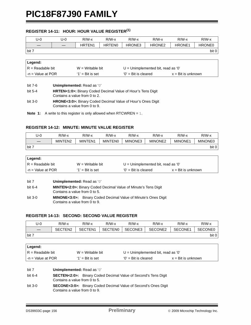
PIC18F87J90 FAMILY
DS39933C-page 156 Preliminary © 2009 Microchip Technology Inc.
REGISTER 14-11: HOUR: HOUR VALUE REGISTER(1)
U-0 U-0 R/W-x R/W-x R/W-x R/W-x R/W-x R/W-x— — HRTEN1 HRTEN0 HRONE3 HRONE2 HRONE1 HRONE0
bit 7 bit 0
Legend:R = Readable bit W = Writable bit U = Unimplemented bit, read as ‘0’-n = Value at POR ‘1’ = Bit is set ‘0’ = Bit is cleared x = Bit is unknown
bit 7-6 Unimplemented: Read as ‘0’bit 5-4 HRTEN<1:0>: Binary Coded Decimal Value of Hour’s Tens Digit
Contains a value from 0 to 2.bit 3-0 HRONE<3:0>: Binary Coded Decimal Value of Hour’s Ones Digit
Contains a value from 0 to 9.
Note 1: A write to this register is only allowed when RTCWREN = 1.
REGISTER 14-12: MINUTE: MINUTE VALUE REGISTER
U-0 R/W-x R/W-x R/W-x R/W-x R/W-x R/W-x R/W-x— MINTEN2 MINTEN1 MINTEN0 MINONE3 MINONE2 MINONE1 MINONE0
bit 7 bit 0
Legend:R = Readable bit W = Writable bit U = Unimplemented bit, read as ‘0’-n = Value at POR ‘1’ = Bit is set ‘0’ = Bit is cleared x = Bit is unknown
bit 7 Unimplemented: Read as ‘0’bit 6-4 MINTEN<2:0>: Binary Coded Decimal Value of Minute’s Tens Digit
Contains a value from 0 to 5.bit 3-0 MINONE<3:0>: Binary Coded Decimal Value of Minute’s Ones Digit
Contains a value from 0 to 9.
REGISTER 14-13: SECOND: SECOND VALUE REGISTER
U-0 R/W-x R/W-x R/W-x R/W-x R/W-x R/W-x R/W-x— SECTEN2 SECTEN1 SECTEN0 SECONE3 SECONE2 SECONE1 SECONE0
bit 7 bit 0
Legend:R = Readable bit W = Writable bit U = Unimplemented bit, read as ‘0’-n = Value at POR ‘1’ = Bit is set ‘0’ = Bit is cleared x = Bit is unknown
bit 7 Unimplemented: Read as ‘0’bit 6-4 SECTEN<2:0>: Binary Coded Decimal Value of Second’s Tens Digit
Contains a value from 0 to 5.bit 3-0 SECONE<3:0>: Binary Coded Decimal Value of Second’s Ones Digit
Contains a value from 0 to 9.
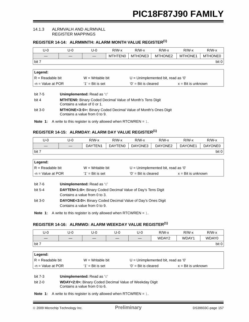
© 2009 Microchip Technology Inc. Preliminary DS39933C-page 157
PIC18F87J90 FAMILY14.1.3 ALRMVALH AND ALRMVALL
REGISTER MAPPINGS
REGISTER 14-14: ALRMMNTH: ALARM MONTH VALUE REGISTER(1)
U-0 U-0 U-0 R/W-x R/W-x R/W-x R/W-x R/W-x— — — MTHTEN0 MTHONE3 MTHONE2 MTHONE1 MTHONE0
bit 7 bit 0
Legend:R = Readable bit W = Writable bit U = Unimplemented bit, read as ‘0’-n = Value at POR ‘1’ = Bit is set ‘0’ = Bit is cleared x = Bit is unknown
bit 7-5 Unimplemented: Read as ‘0’bit 4 MTHTEN0: Binary Coded Decimal Value of Month’s Tens Digit
Contains a value of 0 or 1.bit 3-0 MTHONE<3:0>: Binary Coded Decimal Value of Month’s Ones Digit
Contains a value from 0 to 9.
Note 1: A write to this register is only allowed when RTCWREN = 1.
REGISTER 14-15: ALRMDAY: ALARM DAY VALUE REGISTER(1)
U-0 U-0 R/W-x R/W-x R/W-x R/W-x R/W-x R/W-x— — DAYTEN1 DAYTEN0 DAYONE3 DAYONE2 DAYONE1 DAYONE0
bit 7 bit 0
Legend:R = Readable bit W = Writable bit U = Unimplemented bit, read as ‘0’-n = Value at POR ‘1’ = Bit is set ‘0’ = Bit is cleared x = Bit is unknown
bit 7-6 Unimplemented: Read as ‘0’bit 5-4 DAYTEN<1:0>: Binary Coded Decimal Value of Day’s Tens Digit
Contains a value from 0 to 3.bit 3-0 DAYONE<3:0>: Binary Coded Decimal Value of Day’s Ones Digit
Contains a value from 0 to 9.
Note 1: A write to this register is only allowed when RTCWREN = 1.
REGISTER 14-16: ALRMWD: ALARM WEEKDAY VALUE REGISTER(1)
U-0 U-0 U-0 U-0 U-0 R/W-x R/W-x R/W-x— — — — — WDAY2 WDAY1 WDAY0
bit 7 bit 0
Legend:R = Readable bit W = Writable bit U = Unimplemented bit, read as ‘0’-n = Value at POR ‘1’ = Bit is set ‘0’ = Bit is cleared x = Bit is unknown
bit 7-3 Unimplemented: Read as ‘0’bit 2-0 WDAY<2:0>: Binary Coded Decimal Value of Weekday Digit
Contains a value from 0 to 6.
Note 1: A write to this register is only allowed when RTCWREN = 1.
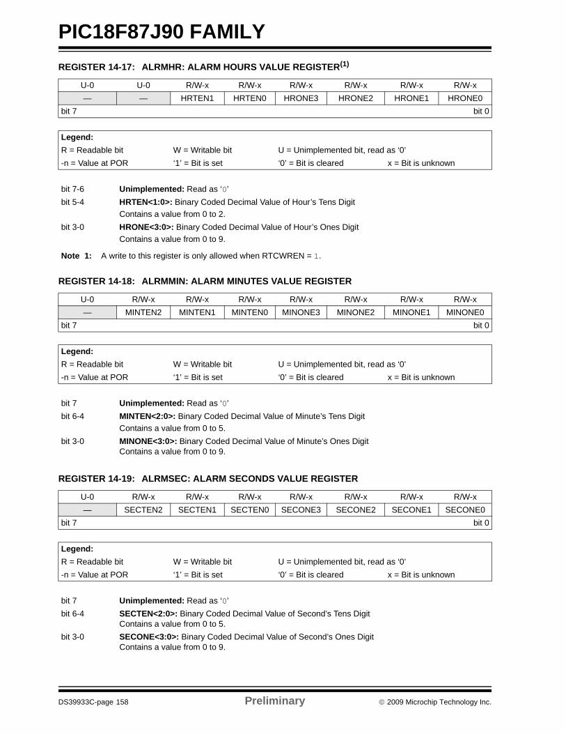
PIC18F87J90 FAMILY
DS39933C-page 158 Preliminary © 2009 Microchip Technology Inc.
REGISTER 14-17: ALRMHR: ALARM HOURS VALUE REGISTER(1)
U-0 U-0 R/W-x R/W-x R/W-x R/W-x R/W-x R/W-x— — HRTEN1 HRTEN0 HRONE3 HRONE2 HRONE1 HRONE0
bit 7 bit 0
Legend:R = Readable bit W = Writable bit U = Unimplemented bit, read as ‘0’-n = Value at POR ‘1’ = Bit is set ‘0’ = Bit is cleared x = Bit is unknown
bit 7-6 Unimplemented: Read as ‘0’bit 5-4 HRTEN<1:0>: Binary Coded Decimal Value of Hour’s Tens Digit
Contains a value from 0 to 2.bit 3-0 HRONE<3:0>: Binary Coded Decimal Value of Hour’s Ones Digit
Contains a value from 0 to 9.
Note 1: A write to this register is only allowed when RTCWREN = 1.
REGISTER 14-18: ALRMMIN: ALARM MINUTES VALUE REGISTER
U-0 R/W-x R/W-x R/W-x R/W-x R/W-x R/W-x R/W-x— MINTEN2 MINTEN1 MINTEN0 MINONE3 MINONE2 MINONE1 MINONE0
bit 7 bit 0
Legend:R = Readable bit W = Writable bit U = Unimplemented bit, read as ‘0’-n = Value at POR ‘1’ = Bit is set ‘0’ = Bit is cleared x = Bit is unknown
bit 7 Unimplemented: Read as ‘0’bit 6-4 MINTEN<2:0>: Binary Coded Decimal Value of Minute’s Tens Digit
Contains a value from 0 to 5.bit 3-0 MINONE<3:0>: Binary Coded Decimal Value of Minute’s Ones Digit
Contains a value from 0 to 9.
REGISTER 14-19: ALRMSEC: ALARM SECONDS VALUE REGISTER
U-0 R/W-x R/W-x R/W-x R/W-x R/W-x R/W-x R/W-x— SECTEN2 SECTEN1 SECTEN0 SECONE3 SECONE2 SECONE1 SECONE0
bit 7 bit 0
Legend:R = Readable bit W = Writable bit U = Unimplemented bit, read as ‘0’-n = Value at POR ‘1’ = Bit is set ‘0’ = Bit is cleared x = Bit is unknown
bit 7 Unimplemented: Read as ‘0’bit 6-4 SECTEN<2:0>: Binary Coded Decimal Value of Second’s Tens Digit
Contains a value from 0 to 5.bit 3-0 SECONE<3:0>: Binary Coded Decimal Value of Second’s Ones Digit
Contains a value from 0 to 9.
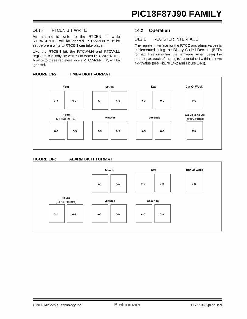
© 2009 Microchip Technology Inc. Preliminary DS39933C-page 159
PIC18F87J90 FAMILY14.1.4 RTCEN BIT WRITEAn attempt to write to the RTCEN bit whileRTCWREN = 0 will be ignored. RTCWREN must beset before a write to RTCEN can take place.
Like the RTCEN bit, the RTCVALH and RTCVALLregisters can only be written to when RTCWREN = 1.A write to these registers, while RTCWREN = 0, will beignored.
14.2 Operation
14.2.1 REGISTER INTERFACEThe register interface for the RTCC and alarm values isimplemented using the Binary Coded Decimal (BCD)format. This simplifies the firmware, when using themodule, as each of the digits is contained within its own4-bit value (see Figure 14-2 and Figure 14-3).
FIGURE 14-2: TIMER DIGIT FORMAT
FIGURE 14-3: ALARM DIGIT FORMAT
0-60-9 0-9 0-3 0-9
0-9 0-9 0-90-2 0-5 0-5 0/1
Day Of WeekYear Day
Hours(24-hour format) Minutes Seconds
1/2 Second Bit
0-1 0-9
Month
(binary format)
0-60-3 0-9
0-9 0-9 0-90-2 0-5 0-5
Day Of WeekDay
Hours(24-hour format) Minutes Seconds
0-1 0-9
Month
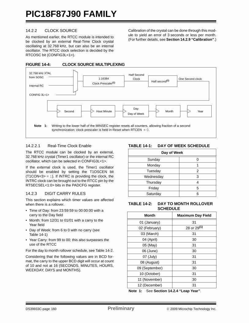
PIC18F87J90 FAMILY
DS39933C-page 160 Preliminary © 2009 Microchip Technology Inc.
14.2.2 CLOCK SOURCEAs mentioned earlier, the RTCC module is intended tobe clocked by an external Real-Time Clock crystaloscillating at 32.768 kHz, but can also be an internaloscillator. The RTCC clock selection is decided by theRTCOSC bit (CONFIG3L<1>).
Calibration of the crystal can be done through this mod-ule to yield an error of 3 seconds or less per month.(For further details, see Section 14.2.9 “Calibration”.)
FIGURE 14-4: CLOCK SOURCE MULTIPLEXING
14.2.2.1 Real-Time Clock EnableThe RTCC module can be clocked by an external,32.768 kHz crystal (Timer1 oscillator) or the internal RCoscillator, which can be selected in CONFIG3L<1>.
If the external clock is used, the Timer1 oscillatorshould be enabled by setting the T1OSCEN bit(T1CON<3> = 1). If INTRC is providing the clock, theINTRC clock can be brought out to the RTCC pin by theRTSECSEL<1:0> bits in the PADCFG register.
14.2.3 DIGIT CARRY RULESThis section explains which timer values are affectedwhen there is a rollover.
• Time of Day: from 23:59:59 to 00:00:00 with a carry to the Day field
• Month: from 12/31 to 01/01 with a carry to the Year field
• Day of Week: from 6 to 0 with no carry (see Table 14-1)
• Year Carry: from 99 to 00; this also surpasses the use of the RTCC
For the day to month rollover schedule, see Table 14-2.
Considering that the following values are in BCD for-mat, the carry to the upper BCD digit will occur at countof 10 and not at 16 (SECONDS, MINUTES, HOURS,WEEKDAY, DAYS and MONTHS).
TABLE 14-1: DAY OF WEEK SCHEDULE
TABLE 14-2: DAY TO MONTH ROLLOVER SCHEDULE
Note 1: Writing to the lower half of the MINSEC register resets all counters, allowing fraction of a second synchronization; clock prescaler is held in Reset when RTCEN = 0.
32.768 kHz XTAL
1:16384Half second(1)
Half SecondClock One Second clock
YearMonthDay
Day of WeekSecond Hour:Minute
Clock Prescaler(1)
from SOSC
Internal RC
CONFIG 3L<1>
Day of Week
Sunday 0Monday 1Tuesday 2
Wednesday 3Thursday 4
Friday 5Saturday 6
Month Maximum Day Field
01 (January) 3102 (February) 28 or 29(1)
03 (March) 3104 (April) 3005 (May) 3106 (June) 3007 (July) 31
08 (August) 3109 (September) 30
10 (October) 3111 (November) 3012 (December) 31
Note 1: See Section 14.2.4 “Leap Year”.
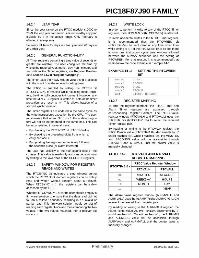
© 2009 Microchip Technology Inc. Preliminary DS39933C-page 161
PIC18F87J90 FAMILY14.2.4 LEAP YEARSince the year range on the RTCC module is 2000 to2099, the leap year calculation is determined by any yeardivisible by 4 in the above range. Only February iseffected in a leap year.
February will have 29 days in a leap year and 28 days inany other year.
14.2.5 GENERAL FUNCTIONALITYAll Timer registers containing a time value of seconds orgreater are writable. The user configures the time bywriting the required year, month, day, hour, minutes andseconds to the Timer registers, via Register Pointers(see Section 14.2.8 “Register Mapping”).
The timer uses the newly written values and proceedswith the count from the required starting point.
The RTCC is enabled by setting the RTCEN bit(RTCCFG<7>). If enabled while adjusting these regis-ters, the timer still continues to increment. However, anytime the MINSEC register is written to, both of the timerprescalers are reset to ‘0’. This allows fraction of asecond synchronization.
The Timer registers are updated in the same cycle asthe write instruction’s execution by the CPU. The usermust ensure that when RTCEN = 1, the updated regis-ters will not be incremented at the same time. This canbe accomplished in several ways:
• By checking the RTCSYNC bit (RTCCFG<4>)• By checking the preceding digits from which a
carry can occur• By updating the registers immediately following
the seconds pulse (or alarm interrupt)
The user has visibility to the half-second field of thecounter. This value is read-only and can be reset onlyby writing to the lower half of the SECONDS register.
14.2.6 SAFETY WINDOW FOR REGISTER READS AND WRITES
The RTCSYNC bit indicates a time window duringwhich the RTCC clock domain registers can be safelyread and written without concern about a rollover.When RTCSYNC = 0, the registers can be safelyaccessed by the CPU.
Whether RTCSYNC = 1 or 0, the user should employ afirmware solution to ensure that the data read did notfall on a rollover boundary, resulting in an invalid orpartial read. This firmware solution would consist ofreading each register twice and then comparing the twovalues. If the two values matched, then a rollover didnot occur.
14.2.7 WRITE LOCKIn order to perform a write to any of the RTCC Timerregisters, the RTCWREN bit (RTCCFG<5>) must be set.
To avoid accidental writes to the RTCC Timer register,it is recommended that the RTCWREN bit(RTCCFG<5>) be kept clear at any time other thanwhile writing to it. For the RTCWREN bit to be set, thereis only one instruction cycle time window allowedbetween the 55h/AA sequence and the setting ofRTCWREN. For that reason, it is recommended thatusers follow the code example in Example 14-1.
EXAMPLE 14-1: SETTING THE RTCWREN BIT
14.2.8 REGISTER MAPPINGTo limit the register interface, the RTCC Timer andAlarm Timer registers are accessed throughcorresponding Register Pointers. The RTCC Valueregister window (RTCVALH and RTCVALL) uses theRTCPTR bits (RTCCFG<1:0>) to select the requiredTimer register pair.
By reading or writing to the RTCVALH register, theRTCC Pointer value (RTCPTR<1:0>) decrements by ‘1’until it reaches ‘00’. Once it reaches ‘00’, the MINUTESand SECONDS value will be accessible throughRTCVALH and RTCVALL until the pointer value ismanually changed.
TABLE 14-3: RTCVALH AND RTCVALL REGISTER MAPPING
The Alarm Value register window (ALRMVALH andALRMVALL) uses the ALRMPTR bits (ALRMCFG<1:0>)to select the desired Alarm register pair.
By reading or writing to the ALRMVALH register, theAlarm Pointer value, ALRMPTR<1:0>, decrements by ‘1’until it reaches ‘00’. Once it reaches ‘00’, the ALRMMINand ALRMSEC value will be accessible throughALRMVALH and ALRMVALL until the pointer value ismanually changed.
movlw 0x55movwf EECON2movlw 0xAAmovwf EECON2bsf RTCCFG,RTCWREN
RTCPTR<1:0>RTCC Value Register Window
RTCVALH RTCVALL
00 MINUTES SECONDS01 WEEKDAY HOURS10 MONTH DAY11 — YEAR
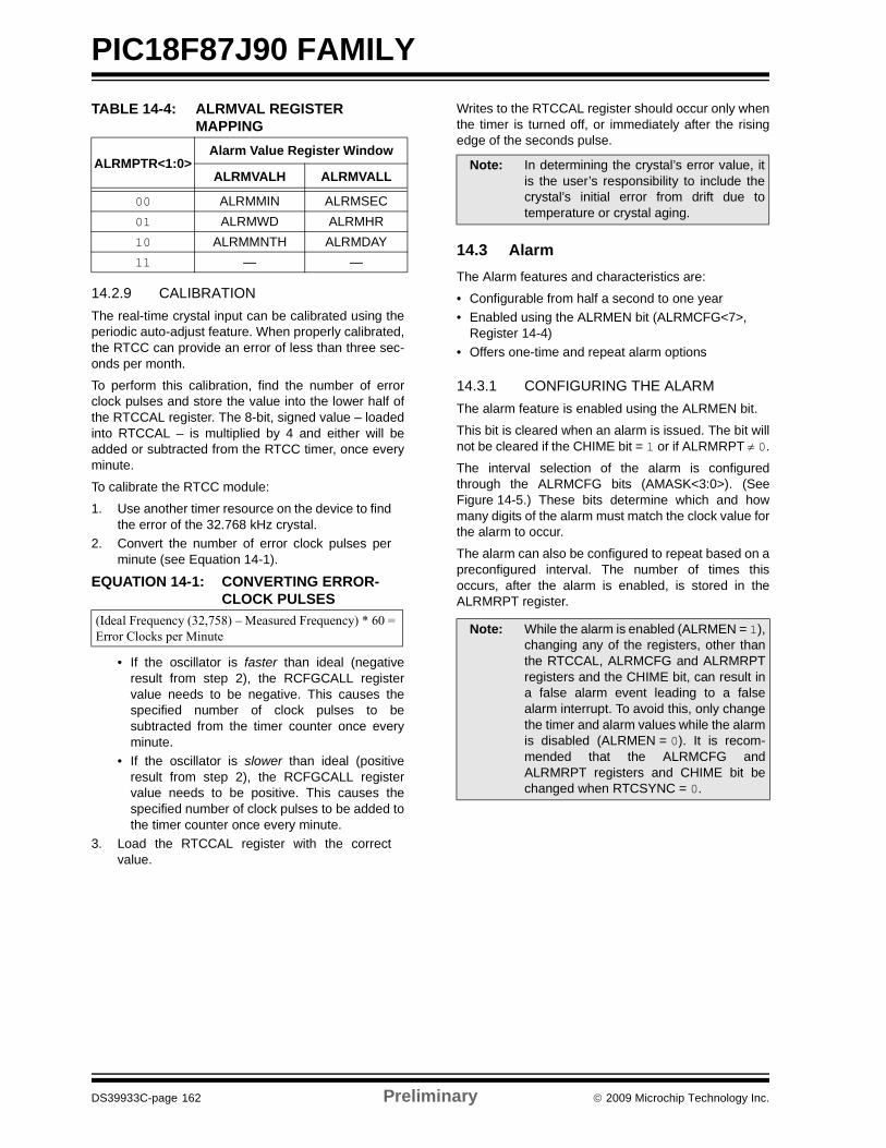
PIC18F87J90 FAMILY
DS39933C-page 162 Preliminary © 2009 Microchip Technology Inc.
TABLE 14-4: ALRMVAL REGISTER MAPPING
14.2.9 CALIBRATIONThe real-time crystal input can be calibrated using theperiodic auto-adjust feature. When properly calibrated,the RTCC can provide an error of less than three sec-onds per month.
To perform this calibration, find the number of errorclock pulses and store the value into the lower half ofthe RTCCAL register. The 8-bit, signed value – loadedinto RTCCAL – is multiplied by 4 and either will beadded or subtracted from the RTCC timer, once everyminute.
To calibrate the RTCC module:
1. Use another timer resource on the device to findthe error of the 32.768 kHz crystal.
2. Convert the number of error clock pulses perminute (see Equation 14-1).
• If the oscillator is faster than ideal (negativeresult from step 2), the RCFGCALL registervalue needs to be negative. This causes thespecified number of clock pulses to besubtracted from the timer counter once everyminute.
• If the oscillator is slower than ideal (positiveresult from step 2), the RCFGCALL registervalue needs to be positive. This causes thespecified number of clock pulses to be added tothe timer counter once every minute.
3. Load the RTCCAL register with the correctvalue.
Writes to the RTCCAL register should occur only whenthe timer is turned off, or immediately after the risingedge of the seconds pulse.
14.3 AlarmThe Alarm features and characteristics are:
• Configurable from half a second to one year• Enabled using the ALRMEN bit (ALRMCFG<7>,
Register 14-4)• Offers one-time and repeat alarm options
14.3.1 CONFIGURING THE ALARMThe alarm feature is enabled using the ALRMEN bit.
This bit is cleared when an alarm is issued. The bit willnot be cleared if the CHIME bit = 1 or if ALRMRPT ≠ 0.
The interval selection of the alarm is configuredthrough the ALRMCFG bits (AMASK<3:0>). (SeeFigure 14-5.) These bits determine which and howmany digits of the alarm must match the clock value forthe alarm to occur.
The alarm can also be configured to repeat based on apreconfigured interval. The number of times thisoccurs, after the alarm is enabled, is stored in theALRMRPT register.
ALRMPTR<1:0>Alarm Value Register Window
ALRMVALH ALRMVALL
00 ALRMMIN ALRMSEC01 ALRMWD ALRMHR10 ALRMMNTH ALRMDAY11 — —
EQUATION 14-1: CONVERTING ERROR-CLOCK PULSES
(Ideal Frequency (32,758) – Measured Frequency) * 60 = Error Clocks per Minute
Note: In determining the crystal’s error value, itis the user’s responsibility to include thecrystal’s initial error from drift due totemperature or crystal aging.
Note: While the alarm is enabled (ALRMEN = 1),changing any of the registers, other thanthe RTCCAL, ALRMCFG and ALRMRPTregisters and the CHIME bit, can result ina false alarm event leading to a falsealarm interrupt. To avoid this, only changethe timer and alarm values while the alarmis disabled (ALRMEN = 0). It is recom-mended that the ALRMCFG andALRMRPT registers and CHIME bit bechanged when RTCSYNC = 0.
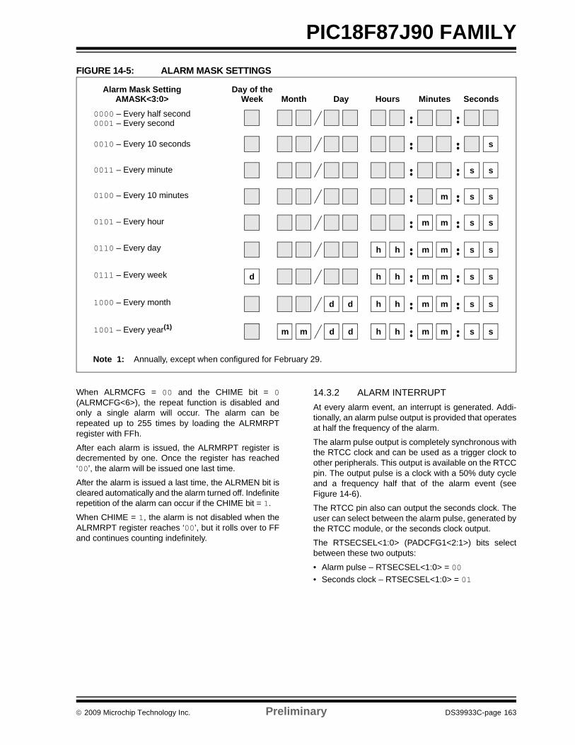
© 2009 Microchip Technology Inc. Preliminary DS39933C-page 163
PIC18F87J90 FAMILYFIGURE 14-5: ALARM MASK SETTINGS
When ALRMCFG = 00 and the CHIME bit = 0(ALRMCFG<6>), the repeat function is disabled andonly a single alarm will occur. The alarm can berepeated up to 255 times by loading the ALRMRPTregister with FFh.
After each alarm is issued, the ALRMRPT register isdecremented by one. Once the register has reached‘00’, the alarm will be issued one last time.
After the alarm is issued a last time, the ALRMEN bit iscleared automatically and the alarm turned off. Indefiniterepetition of the alarm can occur if the CHIME bit = 1.
When CHIME = 1, the alarm is not disabled when theALRMRPT register reaches ‘00’, but it rolls over to FFand continues counting indefinitely.
14.3.2 ALARM INTERRUPTAt every alarm event, an interrupt is generated. Addi-tionally, an alarm pulse output is provided that operatesat half the frequency of the alarm.
The alarm pulse output is completely synchronous withthe RTCC clock and can be used as a trigger clock toother peripherals. This output is available on the RTCCpin. The output pulse is a clock with a 50% duty cycleand a frequency half that of the alarm event (seeFigure 14-6).
The RTCC pin also can output the seconds clock. Theuser can select between the alarm pulse, generated bythe RTCC module, or the seconds clock output.
The RTSECSEL<1:0> (PADCFG1<2:1>) bits selectbetween these two outputs:
• Alarm pulse – RTSECSEL<1:0> = 00• Seconds clock – RTSECSEL<1:0> = 01
Note 1: Annually, except when configured for February 29.
s
s s
m s s
m m s s
h h m m s s
d h h m m s s
d d h h m m s s
m m d d h h m m s s
Day of theWeek Month Day Hours Minutes Seconds
Alarm Mask SettingAMASK<3:0>
0000 – Every half second0001 – Every second
0010 – Every 10 seconds
0011 – Every minute
0100 – Every 10 minutes
0101 – Every hour
0110 – Every day
0111 – Every week
1000 – Every month
1001 – Every year(1)
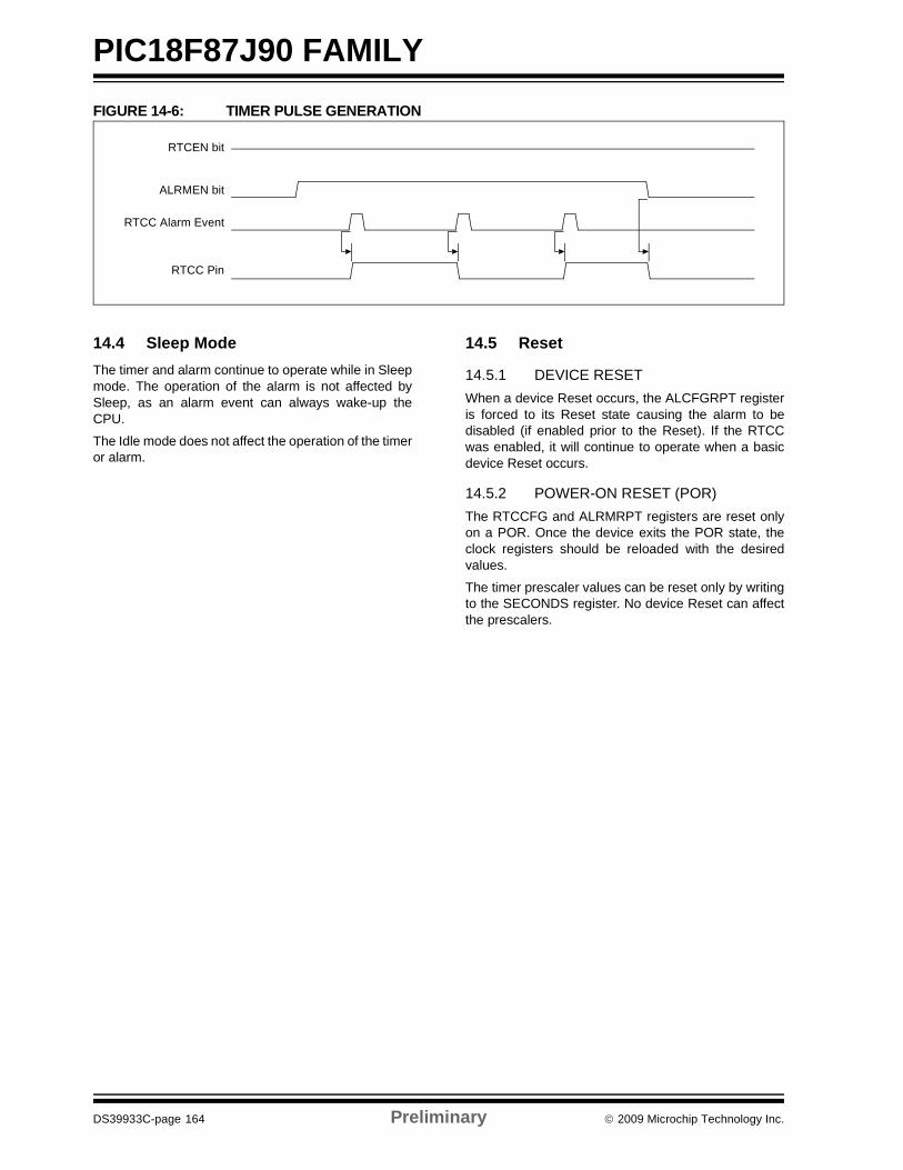
PIC18F87J90 FAMILY
DS39933C-page 164 Preliminary © 2009 Microchip Technology Inc.
FIGURE 14-6: TIMER PULSE GENERATION
14.4 Sleep ModeThe timer and alarm continue to operate while in Sleepmode. The operation of the alarm is not affected bySleep, as an alarm event can always wake-up theCPU.
The Idle mode does not affect the operation of the timeror alarm.
14.5 Reset
14.5.1 DEVICE RESETWhen a device Reset occurs, the ALCFGRPT registeris forced to its Reset state causing the alarm to bedisabled (if enabled prior to the Reset). If the RTCCwas enabled, it will continue to operate when a basicdevice Reset occurs.
14.5.2 POWER-ON RESET (POR)The RTCCFG and ALRMRPT registers are reset onlyon a POR. Once the device exits the POR state, theclock registers should be reloaded with the desiredvalues.
The timer prescaler values can be reset only by writingto the SECONDS register. No device Reset can affectthe prescalers.
RTCEN bit
ALRMEN bit
RTCC Alarm Event
RTCC Pin
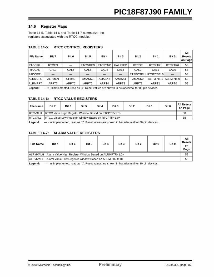
© 2009 Microchip Technology Inc. Preliminary DS39933C-page 165
PIC18F87J90 FAMILY14.6 Register MapsTable 14-5, Table 14-6 and Table 14-7 summarize theregisters associated with the RTCC module.
TABLE 14-5: RTCC CONTROL REGISTERS
File Name Bit 7 Bit 6 Bit 5 Bit 4 Bit 3 Bit 2 Bit 1 Bit 0All
Resetson Page
RTCCFG RTCEN — RTCWREN RTCSYNC HALFSEC RTCOE RTCPTR1 RTCPTR0 58RTCCAL CAL7 CAL6 CAL5 CAL4 CAL3 CAL2 CAL1 CAL0 58PADCFG1 — — — — — RTSECSEL1 RTSECSEL0 — 58ALRMCFG ALRMEN CHIME AMASK3 AMASK2 AMASK1 AMASK0 ALRMPTR1 ALRMPTR0 58ALRMRPT ARPT7 ARPT6 ARPT5 ARPT4 ARPT3 ARPT2 ARPT1 ARPT0 58Legend: — = unimplemented, read as ‘0’. Reset values are shown in hexadecimal for 80-pin devices.
TABLE 14-6: RTCC VALUE REGISTERS
File Name Bit 7 Bit 6 Bit 5 Bit 4 Bit 3 Bit 2 Bit 1 Bit 0 All Resetson Page
RTCVALH RTCC Value High Register Window Based on RTCPTR<1:0> 58RTCVALL RTCC Value Low Register Window Based on RTCPTR<1:0> 58Legend: — = unimplemented, read as ‘0’. Reset values are shown in hexadecimal for 80-pin devices.
TABLE 14-7: ALARM VALUE REGISTERS
File Name Bit 7 Bit 6 Bit 5 Bit 4 Bit 3 Bit 2 Bit 1 Bit 0
All Resets
on Page
ALRMVALH Alarm Value High Register Window Based on ALRMPTR<1:0> 58ALRMVALL Alarm Value Low Register Window Based on ALRMPTR<1:0> 58Legend: — = unimplemented, read as ‘0’. Reset values are shown in hexadecimal for 80-pin devices.

PIC18F87J90 FAMILY
DS39933C-page 166 Preliminary © 2009 Microchip Technology Inc.
NOTES:
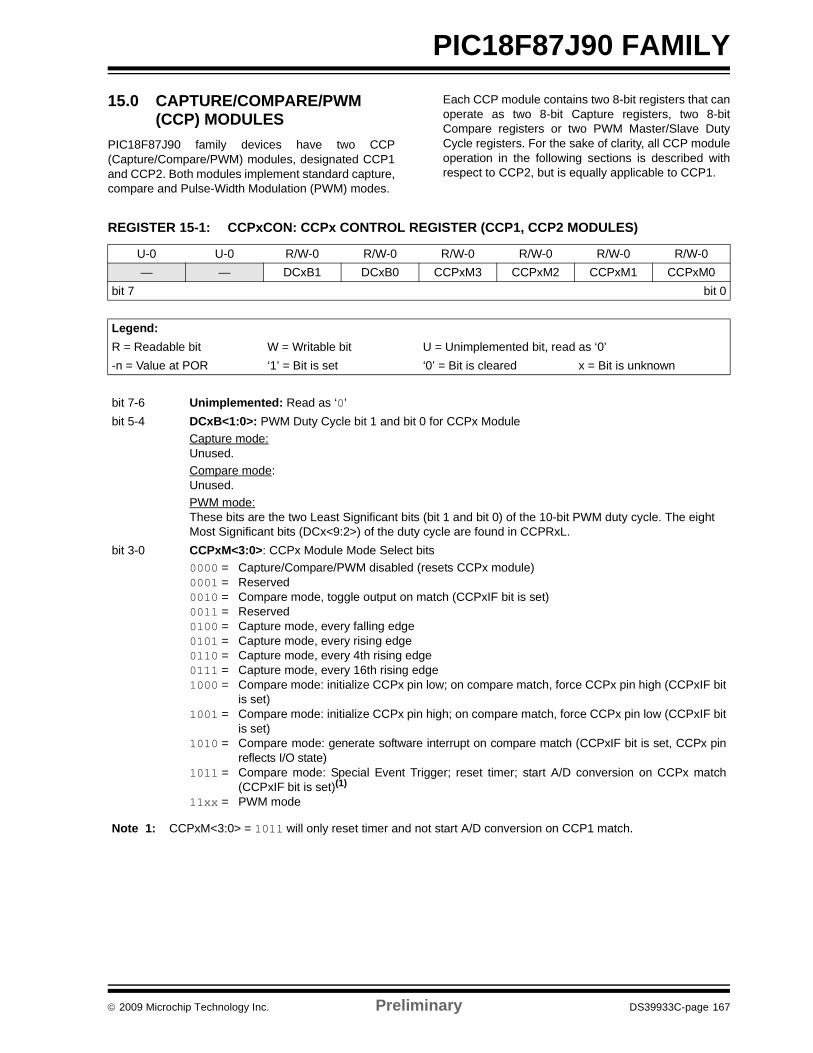
© 2009 Microchip Technology Inc. Preliminary DS39933C-page 167
PIC18F87J90 FAMILY
15.0 CAPTURE/COMPARE/PWM (CCP) MODULES
PIC18F87J90 family devices have two CCP(Capture/Compare/PWM) modules, designated CCP1and CCP2. Both modules implement standard capture,compare and Pulse-Width Modulation (PWM) modes.
Each CCP module contains two 8-bit registers that canoperate as two 8-bit Capture registers, two 8-bitCompare registers or two PWM Master/Slave DutyCycle registers. For the sake of clarity, all CCP moduleoperation in the following sections is described withrespect to CCP2, but is equally applicable to CCP1.
REGISTER 15-1: CCPxCON: CCPx CONTROL REGISTER (CCP1, CCP2 MODULES)
U-0 U-0 R/W-0 R/W-0 R/W-0 R/W-0 R/W-0 R/W-0— — DCxB1 DCxB0 CCPxM3 CCPxM2 CCPxM1 CCPxM0
bit 7 bit 0
Legend:R = Readable bit W = Writable bit U = Unimplemented bit, read as ‘0’-n = Value at POR ‘1’ = Bit is set ‘0’ = Bit is cleared x = Bit is unknown
bit 7-6 Unimplemented: Read as ‘0’bit 5-4 DCxB<1:0>: PWM Duty Cycle bit 1 and bit 0 for CCPx Module
Capture mode:Unused.Compare mode:Unused.PWM mode:These bits are the two Least Significant bits (bit 1 and bit 0) of the 10-bit PWM duty cycle. The eight Most Significant bits (DCx<9:2>) of the duty cycle are found in CCPRxL.
bit 3-0 CCPxM<3:0>: CCPx Module Mode Select bits0000 = Capture/Compare/PWM disabled (resets CCPx module) 0001 = Reserved 0010 = Compare mode, toggle output on match (CCPxIF bit is set) 0011 = Reserved 0100 = Capture mode, every falling edge 0101 = Capture mode, every rising edge0110 = Capture mode, every 4th rising edge 0111 = Capture mode, every 16th rising edge1000 = Compare mode: initialize CCPx pin low; on compare match, force CCPx pin high (CCPxIF bit
is set)1001 = Compare mode: initialize CCPx pin high; on compare match, force CCPx pin low (CCPxIF bit
is set)1010 = Compare mode: generate software interrupt on compare match (CCPxIF bit is set, CCPx pin
reflects I/O state) 1011 = Compare mode: Special Event Trigger; reset timer; start A/D conversion on CCPx match
(CCPxIF bit is set)(1) 11xx = PWM mode
Note 1: CCPxM<3:0> = 1011 will only reset timer and not start A/D conversion on CCP1 match.
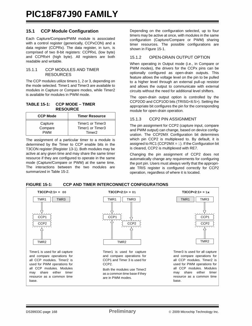
PIC18F87J90 FAMILY
DS39933C-page 168 Preliminary © 2009 Microchip Technology Inc.
15.1 CCP Module ConfigurationEach Capture/Compare/PWM module is associatedwith a control register (generically, CCPxCON) and adata register (CCPRx). The data register, in turn, iscomprised of two 8-bit registers: CCPRxL (low byte)and CCPRxH (high byte). All registers are bothreadable and writable.
15.1.1 CCP MODULES AND TIMER RESOURCES
The CCP modules utilize timers 1, 2 or 3, depending onthe mode selected. Timer1 and Timer3 are available tomodules in Capture or Compare modes, while Timer2is available for modules in PWM mode.
TABLE 15-1: CCP MODE – TIMER RESOURCE
The assignment of a particular timer to a module isdetermined by the Timer to CCP enable bits in theT3CON register (Register 13-1). Both modules may beactive at any given time and may share the same timerresource if they are configured to operate in the samemode (Capture/Compare or PWM) at the same time.The interactions between the two modules aresummarized in Table 15-2.
Depending on the configuration selected, up to fourtimers may be active at once, with modules in the sameconfiguration (Capture/Compare or PWM) sharingtimer resources. The possible configurations areshown in Figure 15-1.
15.1.2 OPEN-DRAIN OUTPUT OPTIONWhen operating in Output mode (i.e., in Compare orPWM modes), the drivers for the CCPx pins can beoptionally configured as open-drain outputs. Thisfeature allows the voltage level on the pin to be pulledto a higher level through an external pull-up resistorand allows the output to communicate with externalcircuits without the need for additional level shifters.
The open-drain output option is controlled by theCCP2OD and CCP1OD bits (TRISG<6:5>). Setting theappropriate bit configures the pin for the correspondingmodule for open-drain operation.
15.1.3 CCP2 PIN ASSIGNMENTThe pin assignment for CCP2 (capture input, compareand PWM output) can change, based on device config-uration. The CCP2MX Configuration bit determineswhich pin CCP2 is multiplexed to. By default, it isassigned to RC1 (CCP2MX = 1). If the Configuration bitis cleared, CCP2 is multiplexed with RE7.
Changing the pin assignment of CCP2 does notautomatically change any requirements for configuringthe port pin. Users must always verify that the appropri-ate TRIS register is configured correctly for CCP2operation, regardless of where it is located.
FIGURE 15-1: CCP AND TIMER INTERCONNECT CONFIGURATIONS
CCP Mode Timer Resource
CaptureCompare
PWM
Timer1 or Timer3Timer1 or Timer3
Timer2
TMR1
TMR2
TMR3
CCP2
CCP1
TMR1
TMR2
TMR3
CCP2
CCP1
TMR1 TMR3
TMR2
CCP2
CCP1
T3CCP<2:1> = 00 T3CCP<2:1> = 01 T3CCP<2:1> = 1x
Timer1 is used for all captureand compare operations forall CCP modules. Timer2 isused for PWM operations forall CCP modules. Modulesmay share either timerresource as a common timebase.
Timer1 is used for captureand compare operations forCCP1 and Timer 3 is used forCCP2.Both the modules use Timer2as a common time base if theyare in PWM modes.
Timer3 is used for all captureand compare operations forall CCP modules. Timer2 isused for PWM operations forall CCP modules. Modulesmay share either timerresource as a common timebase.

© 2009 Microchip Technology Inc. Preliminary DS39933C-page 169
PIC18F87J90 FAMILYTABLE 15-2: INTERACTIONS BETWEEN CCP1 AND CCP2 FOR TIMER RESOURCES CCP1 Mode CCP2 Mode Interaction
Capture Capture Each module can use TMR1 or TMR3 as the time base. The time base can be different for each CCP.
Capture Compare CCP2 can be configured for the Special Event Trigger to reset TMR1 or TMR3 (depending upon which time base is used). Automatic A/D conversions on trigger event can also be done. Operation of CCP1 could be affected if it is using the same timer as a time base.
Compare Capture CCP1 can be configured for the Special Event Trigger to reset TMR1 or TMR3 (depending upon which time base is used). Operation of CCP2 could be affected if it is using the same timer as a time base.
Compare Compare Either module can be configured for the Special Event Trigger to reset the time base. Automatic A/D conversions on CCP2 trigger event can be done. Conflicts may occur if both modules are using the same time base.
Capture PWM NoneCompare PWM None
PWM Capture NonePWM Compare NonePWM PWM Both PWMs will have the same frequency and update rate (TMR2 interrupt).
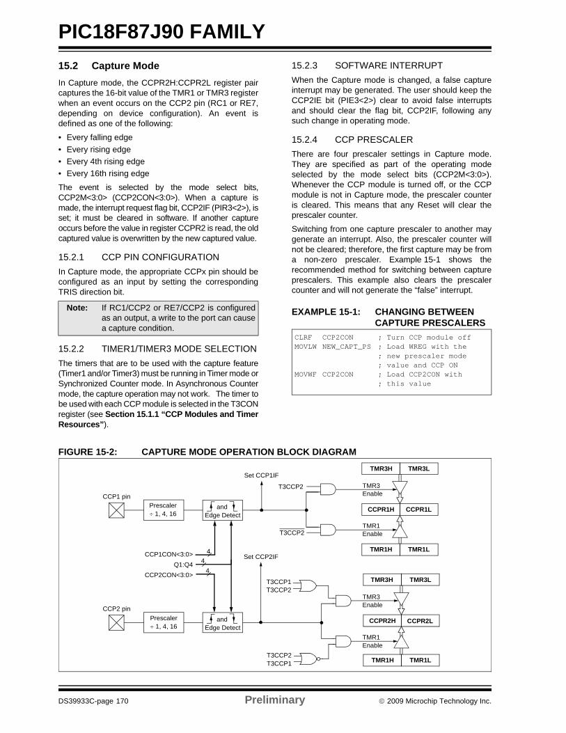
PIC18F87J90 FAMILY
DS39933C-page 170 Preliminary © 2009 Microchip Technology Inc.
15.2 Capture ModeIn Capture mode, the CCPR2H:CCPR2L register paircaptures the 16-bit value of the TMR1 or TMR3 registerwhen an event occurs on the CCP2 pin (RC1 or RE7,depending on device configuration). An event isdefined as one of the following:
• Every falling edge• Every rising edge• Every 4th rising edge• Every 16th rising edge
The event is selected by the mode select bits,CCP2M<3:0> (CCP2CON<3:0>). When a capture ismade, the interrupt request flag bit, CCP2IF (PIR3<2>), isset; it must be cleared in software. If another captureoccurs before the value in register CCPR2 is read, the oldcaptured value is overwritten by the new captured value.
15.2.1 CCP PIN CONFIGURATIONIn Capture mode, the appropriate CCPx pin should beconfigured as an input by setting the correspondingTRIS direction bit.
15.2.2 TIMER1/TIMER3 MODE SELECTIONThe timers that are to be used with the capture feature(Timer1 and/or Timer3) must be running in Timer mode orSynchronized Counter mode. In Asynchronous Countermode, the capture operation may not work. The timer tobe used with each CCP module is selected in the T3CONregister (see Section 15.1.1 “CCP Modules and TimerResources”).
15.2.3 SOFTWARE INTERRUPTWhen the Capture mode is changed, a false captureinterrupt may be generated. The user should keep theCCP2IE bit (PIE3<2>) clear to avoid false interruptsand should clear the flag bit, CCP2IF, following anysuch change in operating mode.
15.2.4 CCP PRESCALERThere are four prescaler settings in Capture mode.They are specified as part of the operating modeselected by the mode select bits (CCP2M<3:0>).Whenever the CCP module is turned off, or the CCPmodule is not in Capture mode, the prescaler counteris cleared. This means that any Reset will clear theprescaler counter.
Switching from one capture prescaler to another maygenerate an interrupt. Also, the prescaler counter willnot be cleared; therefore, the first capture may be froma non-zero prescaler. Example 15-1 shows therecommended method for switching between captureprescalers. This example also clears the prescalercounter and will not generate the “false” interrupt.
EXAMPLE 15-1: CHANGING BETWEEN CAPTURE PRESCALERS
FIGURE 15-2: CAPTURE MODE OPERATION BLOCK DIAGRAM
Note: If RC1/CCP2 or RE7/CCP2 is configuredas an output, a write to the port can causea capture condition.
CLRF CCP2CON ; Turn CCP module offMOVLW NEW_CAPT_PS ; Load WREG with the
; new prescaler mode; value and CCP ON
MOVWF CCP2CON ; Load CCP2CON with; this value
CCPR1H CCPR1L
TMR1H TMR1L
Set CCP1IFTMR3Enable
Q1:Q4CCP1CON<3:0>
CCP1 pinPrescaler÷ 1, 4, 16
andEdge Detect
TMR1Enable
T3CCP2
T3CCP2
CCPR2H CCPR2L
TMR1H TMR1L
Set CCP2IF
TMR3Enable
CCP2CON<3:0>
CCP2 pinPrescaler÷ 1, 4, 16
TMR3H TMR3L
TMR1Enable
T3CCP2T3CCP1
T3CCP2T3CCP1
TMR3H TMR3L
andEdge Detect
44
4
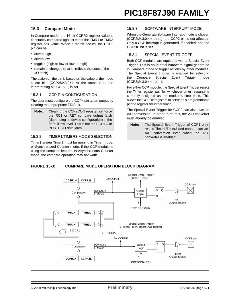
© 2009 Microchip Technology Inc. Preliminary DS39933C-page 171
PIC18F87J90 FAMILY15.3 Compare ModeIn Compare mode, the 16-bit CCPR2 register value isconstantly compared against either the TMR1 or TMR3register pair value. When a match occurs, the CCP2pin can be:
• driven high• driven low• toggled (high-to-low or low-to-high) • remain unchanged (that is, reflects the state of the
I/O latch)
The action on the pin is based on the value of the modeselect bits (CCP2M<3:0>). At the same time, theinterrupt flag bit, CCP2IF, is set.
15.3.1 CCP PIN CONFIGURATIONThe user must configure the CCPx pin as an output byclearing the appropriate TRIS bit.
15.3.2 TIMER1/TIMER3 MODE SELECTIONTimer1 and/or Timer3 must be running in Timer mode,or Synchronized Counter mode, if the CCP module isusing the compare feature. In Asynchronous Countermode, the compare operation may not work.
15.3.3 SOFTWARE INTERRUPT MODE When the Generate Software Interrupt mode is chosen(CCP2M<3:0> = 1010), the CCP2 pin is not affected.Only a CCP interrupt is generated, if enabled, and theCCP2IE bit is set.
15.3.4 SPECIAL EVENT TRIGGERBoth CCP modules are equipped with a Special EventTrigger. This is an internal hardware signal generatedin Compare mode to trigger actions by other modules.The Special Event Trigger is enabled by selectingthe Compare Special Event Trigger mode(CCP2M<3:0> = 1011).
For either CCP module, the Special Event Trigger resetsthe Timer register pair for whichever timer resource iscurrently assigned as the module’s time base. Thisallows the CCPRx registers to serve as a programmableperiod register for either timer.
The Special Event Trigger for CCP2 can also start anA/D conversion. In order to do this, the A/D convertermust already be enabled.
FIGURE 15-3: COMPARE MODE OPERATION BLOCK DIAGRAM
Note: Clearing the CCP2CON register will forcethe RC1 or RE7 compare output latch(depending on device configuration) to thedefault low level. This is not the PORTC orPORTE I/O data latch.
Note: The Special Event Trigger of CCP1 onlyresets Timer1/Timer3 and cannot start anA/D conversion even when the A/Dconverter is enabled.
CCPR1H CCPR1L
TMR1H TMR1L
ComparatorQS
R
OutputLogic
Special Event TriggerSet CCP1IF
CCP1 pin
TRIS
CCP1CON<3:0>
Output Enable
TMR3H TMR3L
CCPR2H CCPR2L
Comparator
1
0
T3CCP2T3CCP1
Set CCP2IF
1
0
Compare
4
(Timer1 Reset)
QS
R
OutputLogic
Special Event Trigger
CCP2 pin
TRIS
CCP2CON<3:0>
Output Enable4
(Timer1/Timer3 Reset, A/D Trigger)
Match
CompareMatch
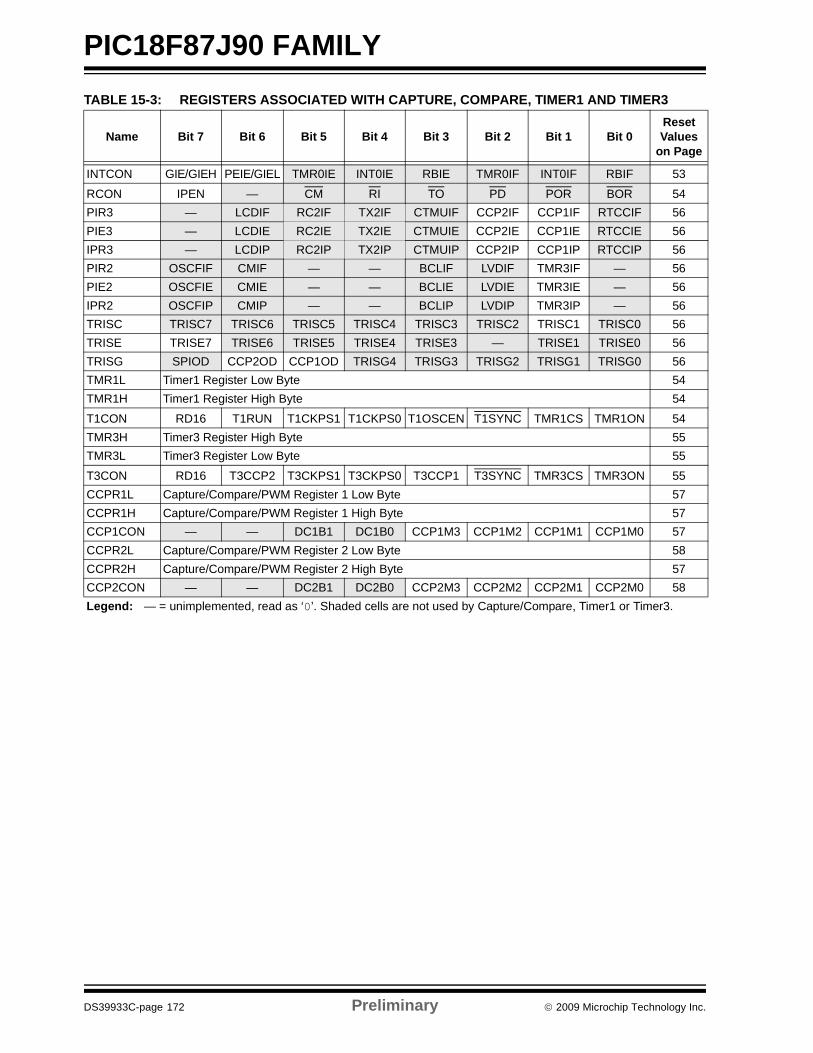
PIC18F87J90 FAMILY
DS39933C-page 172 Preliminary © 2009 Microchip Technology Inc.
TABLE 15-3: REGISTERS ASSOCIATED WITH CAPTURE, COMPARE, TIMER1 AND TIMER3
Name Bit 7 Bit 6 Bit 5 Bit 4 Bit 3 Bit 2 Bit 1 Bit 0Reset Values
on Page
INTCON GIE/GIEH PEIE/GIEL TMR0IE INT0IE RBIE TMR0IF INT0IF RBIF 53
RCON IPEN — CM RI TO PD POR BOR 54PIR3 — LCDIF RC2IF TX2IF CTMUIF CCP2IF CCP1IF RTCCIF 56PIE3 — LCDIE RC2IE TX2IE CTMUIE CCP2IE CCP1IE RTCCIE 56IPR3 — LCDIP RC2IP TX2IP CTMUIP CCP2IP CCP1IP RTCCIP 56PIR2 OSCFIF CMIF — — BCLIF LVDIF TMR3IF — 56PIE2 OSCFIE CMIE — — BCLIE LVDIE TMR3IE — 56IPR2 OSCFIP CMIP — — BCLIP LVDIP TMR3IP — 56TRISC TRISC7 TRISC6 TRISC5 TRISC4 TRISC3 TRISC2 TRISC1 TRISC0 56TRISE TRISE7 TRISE6 TRISE5 TRISE4 TRISE3 — TRISE1 TRISE0 56TRISG SPIOD CCP2OD CCP1OD TRISG4 TRISG3 TRISG2 TRISG1 TRISG0 56TMR1L Timer1 Register Low Byte 54TMR1H Timer1 Register High Byte 54
T1CON RD16 T1RUN T1CKPS1 T1CKPS0 T1OSCEN T1SYNC TMR1CS TMR1ON 54TMR3H Timer3 Register High Byte 55TMR3L Timer3 Register Low Byte 55
T3CON RD16 T3CCP2 T3CKPS1 T3CKPS0 T3CCP1 T3SYNC TMR3CS TMR3ON 55CCPR1L Capture/Compare/PWM Register 1 Low Byte 57CCPR1H Capture/Compare/PWM Register 1 High Byte 57CCP1CON — — DC1B1 DC1B0 CCP1M3 CCP1M2 CCP1M1 CCP1M0 57CCPR2L Capture/Compare/PWM Register 2 Low Byte 58CCPR2H Capture/Compare/PWM Register 2 High Byte 57CCP2CON — — DC2B1 DC2B0 CCP2M3 CCP2M2 CCP2M1 CCP2M0 58Legend: — = unimplemented, read as ‘0’. Shaded cells are not used by Capture/Compare, Timer1 or Timer3.
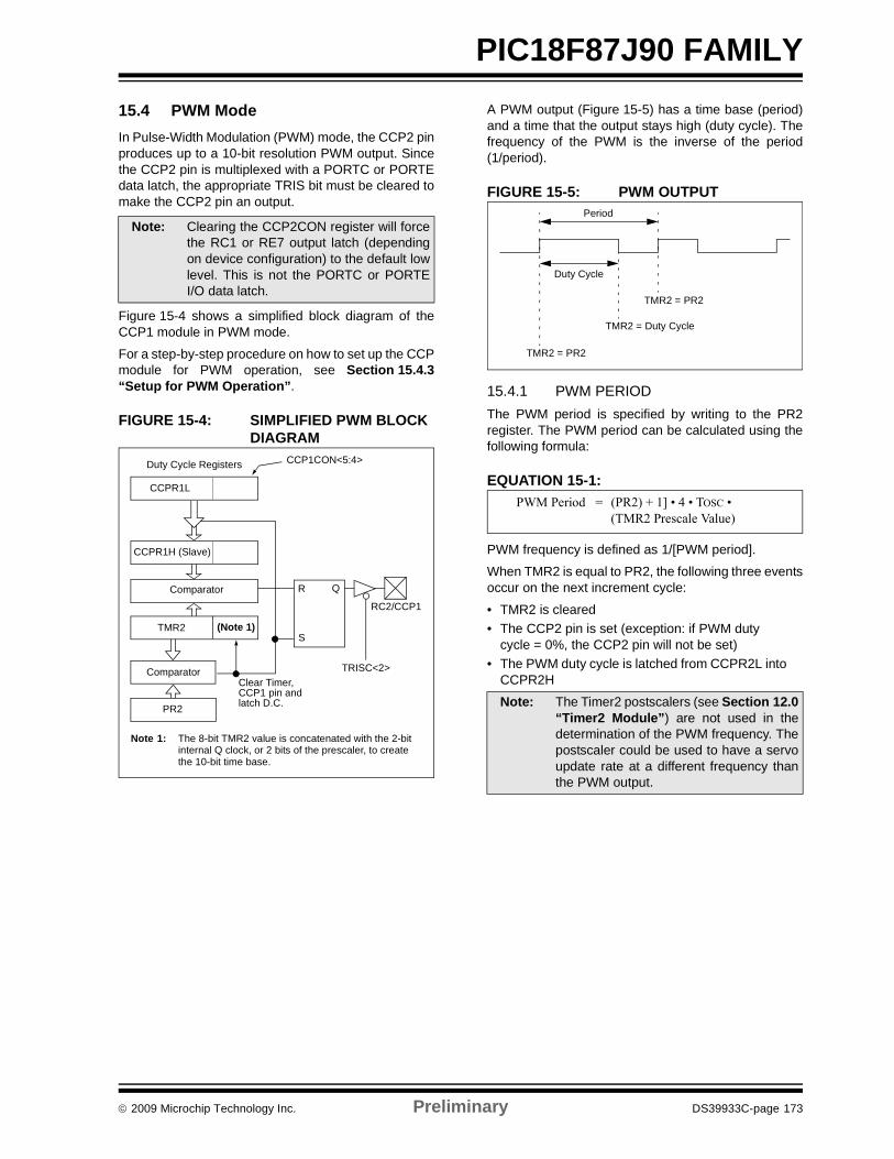
© 2009 Microchip Technology Inc. Preliminary DS39933C-page 173
PIC18F87J90 FAMILY15.4 PWM ModeIn Pulse-Width Modulation (PWM) mode, the CCP2 pinproduces up to a 10-bit resolution PWM output. Sincethe CCP2 pin is multiplexed with a PORTC or PORTEdata latch, the appropriate TRIS bit must be cleared tomake the CCP2 pin an output.
Figure 15-4 shows a simplified block diagram of theCCP1 module in PWM mode.
For a step-by-step procedure on how to set up the CCPmodule for PWM operation, see Section 15.4.3“Setup for PWM Operation”.
FIGURE 15-4: SIMPLIFIED PWM BLOCK DIAGRAM
A PWM output (Figure 15-5) has a time base (period)and a time that the output stays high (duty cycle). Thefrequency of the PWM is the inverse of the period(1/period).
FIGURE 15-5: PWM OUTPUT
15.4.1 PWM PERIODThe PWM period is specified by writing to the PR2register. The PWM period can be calculated using thefollowing formula:
EQUATION 15-1:
PWM frequency is defined as 1/[PWM period].
When TMR2 is equal to PR2, the following three eventsoccur on the next increment cycle:
• TMR2 is cleared• The CCP2 pin is set (exception: if PWM duty
cycle = 0%, the CCP2 pin will not be set)• The PWM duty cycle is latched from CCPR2L into
CCPR2H
Note: Clearing the CCP2CON register will forcethe RC1 or RE7 output latch (dependingon device configuration) to the default lowlevel. This is not the PORTC or PORTEI/O data latch.
CCPR1L
CCPR1H (Slave)
Comparator
TMR2
Comparator
PR2
(Note 1)
R Q
S
Duty Cycle Registers CCP1CON<5:4>
Clear Timer,CCP1 pin and latch D.C.
TRISC<2>
RC2/CCP1
Note 1: The 8-bit TMR2 value is concatenated with the 2-bit internal Q clock, or 2 bits of the prescaler, to create the 10-bit time base.
Note: The Timer2 postscalers (see Section 12.0“Timer2 Module”) are not used in thedetermination of the PWM frequency. Thepostscaler could be used to have a servoupdate rate at a different frequency thanthe PWM output.
Period
Duty Cycle
TMR2 = PR2
TMR2 = Duty Cycle
TMR2 = PR2
PWM Period = (PR2) + 1] • 4 • TOSC •(TMR2 Prescale Value)
PIC18F87J90 FAMILY
DS39933C-page 174 Preliminary © 2009 Microchip Technology Inc.
15.4.2 PWM DUTY CYCLEThe PWM duty cycle is specified by writing to theCCPR2L register and to the CCP2CON<5:4> bits. Upto 10-bit resolution is available. The CCPR2L containsthe eight MSbs and the CCP2CON<5:4> contains thetwo LSbs. This 10-bit value is represented byCCPR2L:CCP2CON<5:4>. The following equation isused to calculate the PWM duty cycle in time:
EQUATION 15-2:
CCPR2L and CCP2CON<5:4> can be written to at anytime, but the duty cycle value is not latched intoCCPR2H until after a match between PR2 and TMR2occurs (i.e., the period is complete). In PWM mode,CCPR2H is a read-only register.
The CCPR2H register and a 2-bit internal latch areused to double-buffer the PWM duty cycle. Thisdouble-buffering is essential for glitchless PWMoperation.
When the CCPR2H and 2-bit latch match TMR2,concatenated with an internal 2-bit Q clock or 2 bits ofthe TMR2 prescaler, the CCP2 pin is cleared.
The maximum PWM resolution (bits) for a given PWMfrequency is given by the equation:
EQUATION 15-3:
TABLE 15-4: EXAMPLE PWM FREQUENCIES AND RESOLUTIONS AT 40 MHz
PWM Duty Cycle = (CCPR2L:CCP2CON<5:4>) •TOSC • (TMR2 Prescale Value)
Note: If the PWM duty cycle value is longer thanthe PWM period, the CCP2 pin will not becleared.
FOSCFPWM---------------⎝ ⎠
⎛ ⎞log
2( )log-----------------------------bits=PWM Resolution (max)
PWM Frequency 2.44 kHz 9.77 kHz 39.06 kHz 156.25 kHz 312.50 kHz 416.67 kHz
Timer Prescaler (1, 4, 16) 16 4 1 1 1 1PR2 Value FFh FFh FFh 3Fh 1Fh 17hMaximum Resolution (bits) 14 12 10 8 7 6.58
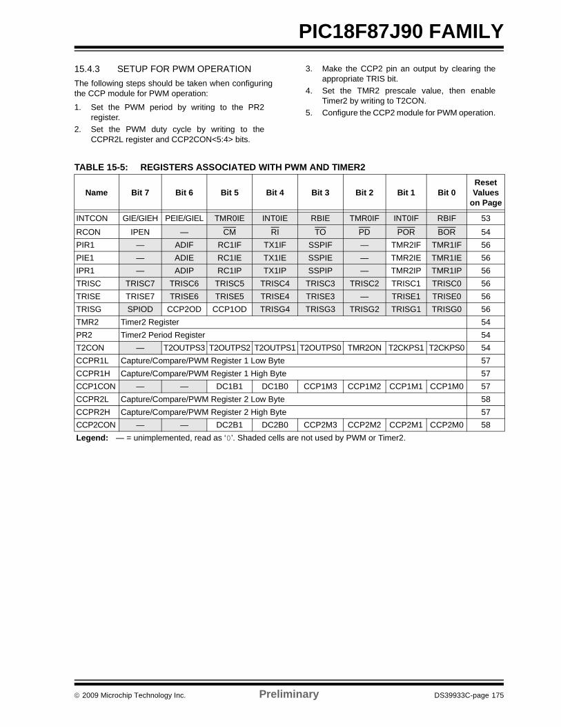
© 2009 Microchip Technology Inc. Preliminary DS39933C-page 175
PIC18F87J90 FAMILY15.4.3 SETUP FOR PWM OPERATIONThe following steps should be taken when configuringthe CCP module for PWM operation:
1. Set the PWM period by writing to the PR2register.
2. Set the PWM duty cycle by writing to theCCPR2L register and CCP2CON<5:4> bits.
3. Make the CCP2 pin an output by clearing theappropriate TRIS bit.
4. Set the TMR2 prescale value, then enableTimer2 by writing to T2CON.
5. Configure the CCP2 module for PWM operation.
TABLE 15-5: REGISTERS ASSOCIATED WITH PWM AND TIMER2
Name Bit 7 Bit 6 Bit 5 Bit 4 Bit 3 Bit 2 Bit 1 Bit 0Reset Values
on Page
INTCON GIE/GIEH PEIE/GIEL TMR0IE INT0IE RBIE TMR0IF INT0IF RBIF 53
RCON IPEN — CM RI TO PD POR BOR 54PIR1 — ADIF RC1IF TX1IF SSPIF — TMR2IF TMR1IF 56PIE1 — ADIE RC1IE TX1IE SSPIE — TMR2IE TMR1IE 56IPR1 — ADIP RC1IP TX1IP SSPIP — TMR2IP TMR1IP 56TRISC TRISC7 TRISC6 TRISC5 TRISC4 TRISC3 TRISC2 TRISC1 TRISC0 56TRISE TRISE7 TRISE6 TRISE5 TRISE4 TRISE3 — TRISE1 TRISE0 56TRISG SPIOD CCP2OD CCP1OD TRISG4 TRISG3 TRISG2 TRISG1 TRISG0 56TMR2 Timer2 Register 54PR2 Timer2 Period Register 54T2CON — T2OUTPS3 T2OUTPS2 T2OUTPS1 T2OUTPS0 TMR2ON T2CKPS1 T2CKPS0 54CCPR1L Capture/Compare/PWM Register 1 Low Byte 57CCPR1H Capture/Compare/PWM Register 1 High Byte 57CCP1CON — — DC1B1 DC1B0 CCP1M3 CCP1M2 CCP1M1 CCP1M0 57CCPR2L Capture/Compare/PWM Register 2 Low Byte 58CCPR2H Capture/Compare/PWM Register 2 High Byte 57CCP2CON — — DC2B1 DC2B0 CCP2M3 CCP2M2 CCP2M1 CCP2M0 58Legend: — = unimplemented, read as ‘0’. Shaded cells are not used by PWM or Timer2.

PIC18F87J90 FAMILY
DS39933C-page 176 Preliminary © 2009 Microchip Technology Inc.
NOTES:
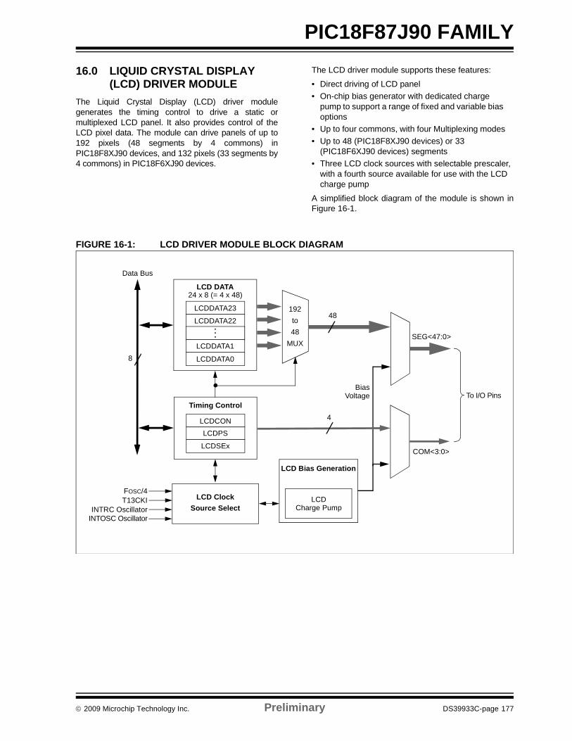
© 2009 Microchip Technology Inc. Preliminary DS39933C-page 177
PIC18F87J90 FAMILY
16.0 LIQUID CRYSTAL DISPLAY (LCD) DRIVER MODULE
The Liquid Crystal Display (LCD) driver modulegenerates the timing control to drive a static ormultiplexed LCD panel. It also provides control of theLCD pixel data. The module can drive panels of up to192 pixels (48 segments by 4 commons) inPIC18F8XJ90 devices, and 132 pixels (33 segments by4 commons) in PIC18F6XJ90 devices.
The LCD driver module supports these features:
• Direct driving of LCD panel• On-chip bias generator with dedicated charge
pump to support a range of fixed and variable bias options
• Up to four commons, with four Multiplexing modes• Up to 48 (PIC18F8XJ90 devices) or 33
(PIC18F6XJ90 devices) segments• Three LCD clock sources with selectable prescaler,
with a fourth source available for use with the LCD charge pump
A simplified block diagram of the module is shown inFigure 16-1.
FIGURE 16-1: LCD DRIVER MODULE BLOCK DIAGRAM
COM<3:0>
Timing Control
Data Bus
INTRC Oscillator
FOSC/4T13CKI
192to48
MUXSEG<47:0>
To I/O Pins
24 x 8 (= 4 x 48)LCD DATA
LCDCONLCDPS
LCDSEx
LCDDATA0
LCDDATA1
LCDDATA22
LCDDATA23
...
LCD Bias Generation
LCD ClockSource Select
LCDCharge Pump
48
4
BiasVoltage
8
INTOSC Oscillator
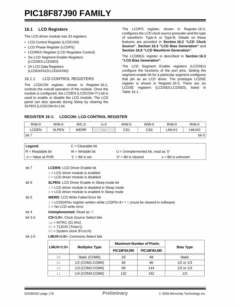
PIC18F87J90 FAMILY
DS39933C-page 178 Preliminary © 2009 Microchip Technology Inc.
16.1 LCD RegistersThe LCD driver module has 33 registers:
• LCD Control Register (LCDCON)• LCD Phase Register (LCDPS)• LCDREG Register (LCD Regulator Control)• Six LCD Segment Enable Registers
(LCDSE5:LCDSE0)• 24 LCD Data Registers
(LCDDATA23:LCDDATA0)
16.1.1 LCD CONTROL REGISTERSThe LCDCON register, shown in Register 16-1,controls the overall operation of the module. Once themodule is configured, the LCDEN (LCDCON<7>) bit isused to enable or disable the LCD module. The LCDpanel can also operate during Sleep by clearing theSLPEN (LCDCON<6>) bit.
The LCDPS register, shown in Register 16-2,configures the LCD clock source prescaler and the typeof waveform: Type-A or Type-B. Details on thesefeatures are provided in Section 16.2 “LCD ClockSource”, Section 16.3 “LCD Bias Generation” andSection 16.8 “LCD Waveform Generation”.
The LCDREG register is described in Section 16.3“LCD Bias Generation”.
The LCD Segment Enable registers (LCDSEx)configure the functions of the port pins. Setting thesegment enable bit for a particular segment configuresthat pin as an LCD driver. The prototype LCDSEregister is shown in Register 16-3. There are sixLCDSE registers (LCDSE5:LCDSE0), listed inTable 16-1.
REGISTER 16-1: LCDCON: LCD CONTROL REGISTER
R/W-0 R/W-0 R/C-0 U-0 R/W-0 R/W-0 R/W-0 R/W-0LCDEN SLPEN WERR — CS1 CS0 LMUX1 LMUX0
bit 7 bit 0
Legend: C = Clearable bitR = Readable bit W = Writable bit U = Unimplemented bit, read as ‘0’-n = Value at POR ‘1’ = Bit is set ‘0’ = Bit is cleared x = Bit is unknown
bit 7 LCDEN: LCD Driver Enable bit1 = LCD driver module is enabled 0 = LCD driver module is disabled
bit 6 SLPEN: LCD Driver Enable in Sleep mode bit1 = LCD driver module is disabled in Sleep mode0 = LCD driver module is enabled in Sleep mode
bit 5 WERR: LCD Write Failed Error bit1 = LCDDATAx register written while LCDPS<4> = 0 (must be cleared in software)0 = No LCD write error
bit 4 Unimplemented: Read as ‘0’bit 3-2 CS<1:0>: Clock Source Select bits
1x = INTRC (31 kHz)01 = T13CKI (Timer1)00 = System clock (FOSC/4)
bit 1-0 LMUX<1:0>: Commons Select bits
LMUX<1:0> Multiplex TypeMaximum Number of Pixels:
Bias TypePIC18F6XJ90 PIC18F8XJ90
00 Static (COM0) 33 48 Static01 1/2 (COM1:COM0) 66 96 1/2 or 1/310 1/3 (COM2:COM0) 99 144 1/2 or 1/311 1/4 (COM3:COM0) 132 192 1/3
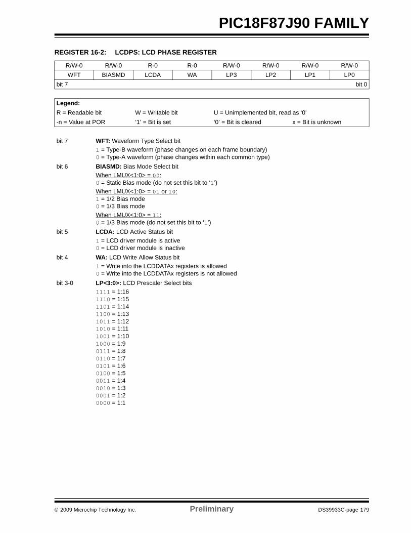
© 2009 Microchip Technology Inc. Preliminary DS39933C-page 179
PIC18F87J90 FAMILY REGISTER 16-2: LCDPS: LCD PHASE REGISTER
R/W-0 R/W-0 R-0 R-0 R/W-0 R/W-0 R/W-0 R/W-0WFT BIASMD LCDA WA LP3 LP2 LP1 LP0
bit 7 bit 0
Legend:R = Readable bit W = Writable bit U = Unimplemented bit, read as ‘0’-n = Value at POR ‘1’ = Bit is set ‘0’ = Bit is cleared x = Bit is unknown
bit 7 WFT: Waveform Type Select bit1 = Type-B waveform (phase changes on each frame boundary)0 = Type-A waveform (phase changes within each common type)
bit 6 BIASMD: Bias Mode Select bitWhen LMUX<1:0> = 00: 0 = Static Bias mode (do not set this bit to ‘1’)When LMUX<1:0> = 01 or 10: 1 = 1/2 Bias mode0 = 1/3 Bias modeWhen LMUX<1:0> = 11: 0 = 1/3 Bias mode (do not set this bit to ‘1’)
bit 5 LCDA: LCD Active Status bit1 = LCD driver module is active0 = LCD driver module is inactive
bit 4 WA: LCD Write Allow Status bit1 = Write into the LCDDATAx registers is allowed0 = Write into the LCDDATAx registers is not allowed
bit 3-0 LP<3:0>: LCD Prescaler Select bits1111 = 1:161110 = 1:151101 = 1:141100 = 1:131011 = 1:121010 = 1:111001 = 1:101000 = 1:90111 = 1:80110 = 1:70101 = 1:60100 = 1:50011 = 1:40010 = 1:30001 = 1:20000 = 1:1
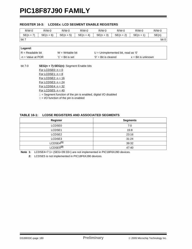
PIC18F87J90 FAMILY
DS39933C-page 180 Preliminary © 2009 Microchip Technology Inc.
TABLE 16-1: LCDSE REGISTERS AND ASSOCIATED SEGMENTS
REGISTER 16-3: LCDSEx: LCD SEGMENT ENABLE REGISTERS
R/W-0 R/W-0 R/W-0 R/W-0 R/W-0 R/W-0 R/W-0 R/W-0SE(n + 7) SE(n + 6) SE(n + 5) SE(n + 4) SE(n + 3) SE(n + 2) SE(n + 1) SE(n)
bit 7 bit 0
Legend:R = Readable bit W = Writable bit U = Unimplemented bit, read as ‘0’-n = Value at POR ‘1’ = Bit is set ‘0’ = Bit is cleared x = Bit is unknown
bit 7-0 SEG(n + 7):SEG(n): Segment Enable bitsFor LCDSE0: n = 0For LCDSE1: n = 8For LCDSE2: n = 16For LCDSE3: n = 24For LCDSE4: n = 32For LCDSE5: n = 401 = Segment function of the pin is enabled, digital I/O disabled0 = I/O function of the pin is enabled
Register Segments
LCDSE0 7:0LCDSE1 15:8LCDSE2 23:16LCDSE3 31:24
LCDSE4(1) 39:32LCDSE5(2) 47:40
Note 1: LCDSE4<7:1> (SEG<39:33>) are not implemented in PIC18F6XJ90 devices. 2: LCDSE5 is not implemented in PIC18F6XJ90 devices.
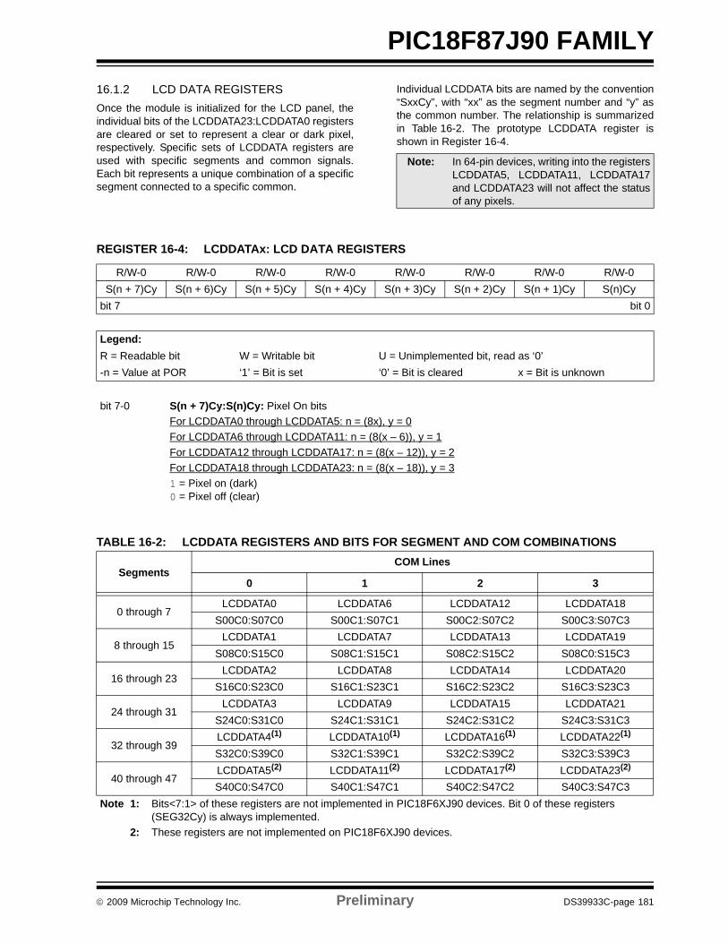
© 2009 Microchip Technology Inc. Preliminary DS39933C-page 181
PIC18F87J90 FAMILY16.1.2 LCD DATA REGISTERSOnce the module is initialized for the LCD panel, theindividual bits of the LCDDATA23:LCDDATA0 registersare cleared or set to represent a clear or dark pixel,respectively. Specific sets of LCDDATA registers areused with specific segments and common signals.Each bit represents a unique combination of a specificsegment connected to a specific common.
Individual LCDDATA bits are named by the convention“SxxCy”, with “xx” as the segment number and “y” asthe common number. The relationship is summarizedin Table 16-2. The prototype LCDDATA register isshown in Register 16-4.
TABLE 16-2: LCDDATA REGISTERS AND BITS FOR SEGMENT AND COM COMBINATIONS
Note: In 64-pin devices, writing into the registersLCDDATA5, LCDDATA11, LCDDATA17and LCDDATA23 will not affect the statusof any pixels.
REGISTER 16-4: LCDDATAx: LCD DATA REGISTERS
R/W-0 R/W-0 R/W-0 R/W-0 R/W-0 R/W-0 R/W-0 R/W-0S(n + 7)Cy S(n + 6)Cy S(n + 5)Cy S(n + 4)Cy S(n + 3)Cy S(n + 2)Cy S(n + 1)Cy S(n)Cy
bit 7 bit 0
Legend:R = Readable bit W = Writable bit U = Unimplemented bit, read as ‘0’-n = Value at POR ‘1’ = Bit is set ‘0’ = Bit is cleared x = Bit is unknown
bit 7-0 S(n + 7)Cy:S(n)Cy: Pixel On bitsFor LCDDATA0 through LCDDATA5: n = (8x), y = 0For LCDDATA6 through LCDDATA11: n = (8(x – 6)), y = 1For LCDDATA12 through LCDDATA17: n = (8(x – 12)), y = 2For LCDDATA18 through LCDDATA23: n = (8(x – 18)), y = 31 = Pixel on (dark)0 = Pixel off (clear)
SegmentsCOM Lines
0 1 2 3
0 through 7LCDDATA0 LCDDATA6 LCDDATA12 LCDDATA18
S00C0:S07C0 S00C1:S07C1 S00C2:S07C2 S00C3:S07C3
8 through 15LCDDATA1 LCDDATA7 LCDDATA13 LCDDATA19
S08C0:S15C0 S08C1:S15C1 S08C2:S15C2 S08C0:S15C3
16 through 23LCDDATA2 LCDDATA8 LCDDATA14 LCDDATA20
S16C0:S23C0 S16C1:S23C1 S16C2:S23C2 S16C3:S23C3
24 through 31LCDDATA3 LCDDATA9 LCDDATA15 LCDDATA21
S24C0:S31C0 S24C1:S31C1 S24C2:S31C2 S24C3:S31C3
32 through 39LCDDATA4(1) LCDDATA10(1) LCDDATA16(1) LCDDATA22(1)
S32C0:S39C0 S32C1:S39C1 S32C2:S39C2 S32C3:S39C3
40 through 47LCDDATA5(2) LCDDATA11(2) LCDDATA17(2) LCDDATA23(2)
S40C0:S47C0 S40C1:S47C1 S40C2:S47C2 S40C3:S47C3Note 1: Bits<7:1> of these registers are not implemented in PIC18F6XJ90 devices. Bit 0 of these registers
(SEG32Cy) is always implemented.2: These registers are not implemented on PIC18F6XJ90 devices.
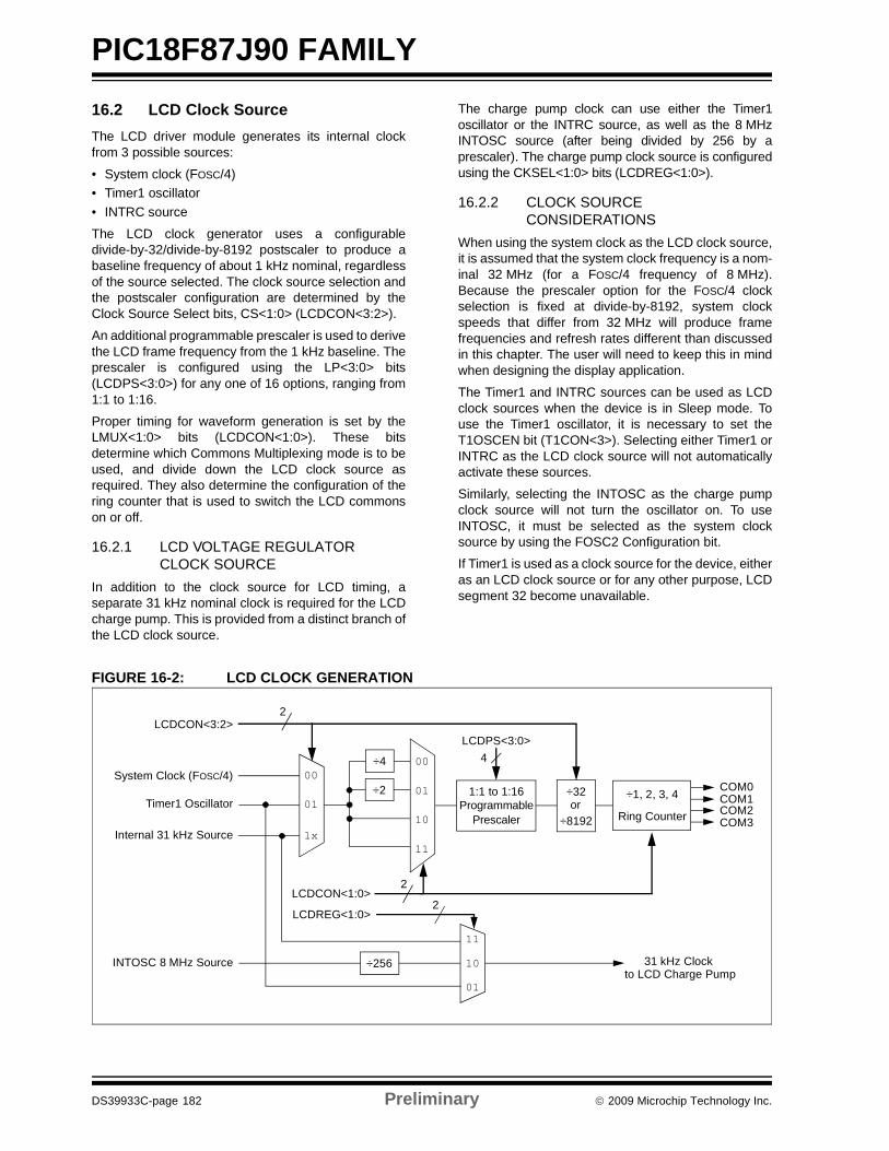
PIC18F87J90 FAMILY
DS39933C-page 182 Preliminary © 2009 Microchip Technology Inc.
16.2 LCD Clock SourceThe LCD driver module generates its internal clockfrom 3 possible sources:
• System clock (FOSC/4)• Timer1 oscillator• INTRC source
The LCD clock generator uses a configurabledivide-by-32/divide-by-8192 postscaler to produce abaseline frequency of about 1 kHz nominal, regardlessof the source selected. The clock source selection andthe postscaler configuration are determined by theClock Source Select bits, CS<1:0> (LCDCON<3:2>).
An additional programmable prescaler is used to derivethe LCD frame frequency from the 1 kHz baseline. Theprescaler is configured using the LP<3:0> bits(LCDPS<3:0>) for any one of 16 options, ranging from1:1 to 1:16.
Proper timing for waveform generation is set by theLMUX<1:0> bits (LCDCON<1:0>). These bitsdetermine which Commons Multiplexing mode is to beused, and divide down the LCD clock source asrequired. They also determine the configuration of thering counter that is used to switch the LCD commonson or off.
16.2.1 LCD VOLTAGE REGULATOR CLOCK SOURCE
In addition to the clock source for LCD timing, aseparate 31 kHz nominal clock is required for the LCDcharge pump. This is provided from a distinct branch ofthe LCD clock source.
The charge pump clock can use either the Timer1oscillator or the INTRC source, as well as the 8 MHzINTOSC source (after being divided by 256 by aprescaler). The charge pump clock source is configuredusing the CKSEL<1:0> bits (LCDREG<1:0>).
16.2.2 CLOCK SOURCE CONSIDERATIONS
When using the system clock as the LCD clock source,it is assumed that the system clock frequency is a nom-inal 32 MHz (for a FOSC/4 frequency of 8 MHz).Because the prescaler option for the FOSC/4 clockselection is fixed at divide-by-8192, system clockspeeds that differ from 32 MHz will produce framefrequencies and refresh rates different than discussedin this chapter. The user will need to keep this in mindwhen designing the display application.
The Timer1 and INTRC sources can be used as LCDclock sources when the device is in Sleep mode. Touse the Timer1 oscillator, it is necessary to set theT1OSCEN bit (T1CON<3>). Selecting either Timer1 orINTRC as the LCD clock source will not automaticallyactivate these sources.
Similarly, selecting the INTOSC as the charge pumpclock source will not turn the oscillator on. To useINTOSC, it must be selected as the system clocksource by using the FOSC2 Configuration bit.
If Timer1 is used as a clock source for the device, eitheras an LCD clock source or for any other purpose, LCDsegment 32 become unavailable.
FIGURE 16-2: LCD CLOCK GENERATION
LCDCON<3:2>
Timer1 Oscillator
Internal 31 kHz Source
÷4
Programmable÷1, 2, 3, 4
Ring Counter
COM0COM1COM2COM3
÷2 ÷32
LCDCON<1:0>
LCDPS<3:0>
System Clock (FOSC/4)
INTOSC 8 MHz Source
1:1 to 1:16
Prescaler1x
01
00
11
10
01
00
31 kHz Clock
11
10
01
LCDREG<1:0>
to LCD Charge Pump
÷8192or
4
2
2
2
÷256
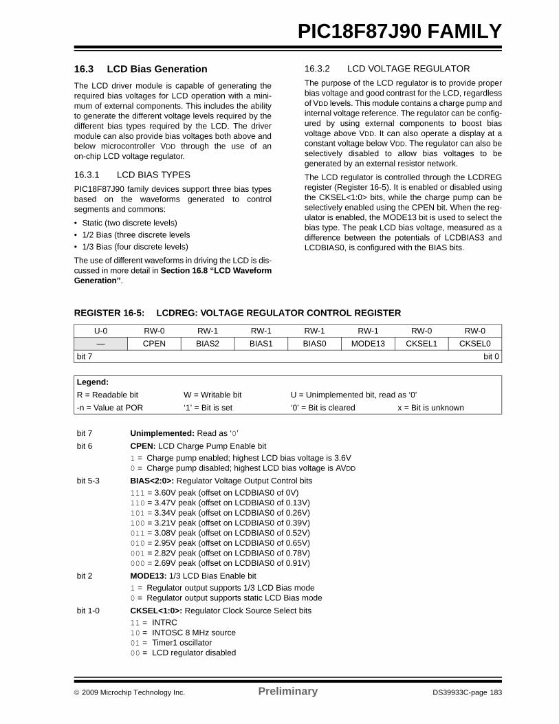
© 2009 Microchip Technology Inc. Preliminary DS39933C-page 183
PIC18F87J90 FAMILY16.3 LCD Bias GenerationThe LCD driver module is capable of generating therequired bias voltages for LCD operation with a mini-mum of external components. This includes the abilityto generate the different voltage levels required by thedifferent bias types required by the LCD. The drivermodule can also provide bias voltages both above andbelow microcontroller VDD through the use of anon-chip LCD voltage regulator.
16.3.1 LCD BIAS TYPESPIC18F87J90 family devices support three bias typesbased on the waveforms generated to controlsegments and commons:
• Static (two discrete levels)• 1/2 Bias (three discrete levels• 1/3 Bias (four discrete levels)
The use of different waveforms in driving the LCD is dis-cussed in more detail in Section 16.8 “LCD WaveformGeneration”.
16.3.2 LCD VOLTAGE REGULATORThe purpose of the LCD regulator is to provide properbias voltage and good contrast for the LCD, regardlessof VDD levels. This module contains a charge pump andinternal voltage reference. The regulator can be config-ured by using external components to boost biasvoltage above VDD. It can also operate a display at aconstant voltage below VDD. The regulator can also beselectively disabled to allow bias voltages to begenerated by an external resistor network.
The LCD regulator is controlled through the LCDREGregister (Register 16-5). It is enabled or disabled usingthe CKSEL<1:0> bits, while the charge pump can beselectively enabled using the CPEN bit. When the reg-ulator is enabled, the MODE13 bit is used to select thebias type. The peak LCD bias voltage, measured as adifference between the potentials of LCDBIAS3 andLCDBIAS0, is configured with the BIAS bits.
REGISTER 16-5: LCDREG: VOLTAGE REGULATOR CONTROL REGISTER
U-0 RW-0 RW-1 RW-1 RW-1 RW-1 RW-0 RW-0— CPEN BIAS2 BIAS1 BIAS0 MODE13 CKSEL1 CKSEL0
bit 7 bit 0
Legend:R = Readable bit W = Writable bit U = Unimplemented bit, read as ‘0’-n = Value at POR ‘1’ = Bit is set ‘0’ = Bit is cleared x = Bit is unknown
bit 7 Unimplemented: Read as ‘0’bit 6 CPEN: LCD Charge Pump Enable bit
1 = Charge pump enabled; highest LCD bias voltage is 3.6V0 = Charge pump disabled; highest LCD bias voltage is AVDD
bit 5-3 BIAS<2:0>: Regulator Voltage Output Control bits111 = 3.60V peak (offset on LCDBIAS0 of 0V)110 = 3.47V peak (offset on LCDBIAS0 of 0.13V)101 = 3.34V peak (offset on LCDBIAS0 of 0.26V)100 = 3.21V peak (offset on LCDBIAS0 of 0.39V)011 = 3.08V peak (offset on LCDBIAS0 of 0.52V)010 = 2.95V peak (offset on LCDBIAS0 of 0.65V) 001 = 2.82V peak (offset on LCDBIAS0 of 0.78V)000 = 2.69V peak (offset on LCDBIAS0 of 0.91V)
bit 2 MODE13: 1/3 LCD Bias Enable bit1 = Regulator output supports 1/3 LCD Bias mode0 = Regulator output supports static LCD Bias mode
bit 1-0 CKSEL<1:0>: Regulator Clock Source Select bits11 = INTRC10 = INTOSC 8 MHz source01 = Timer1 oscillator00 = LCD regulator disabled
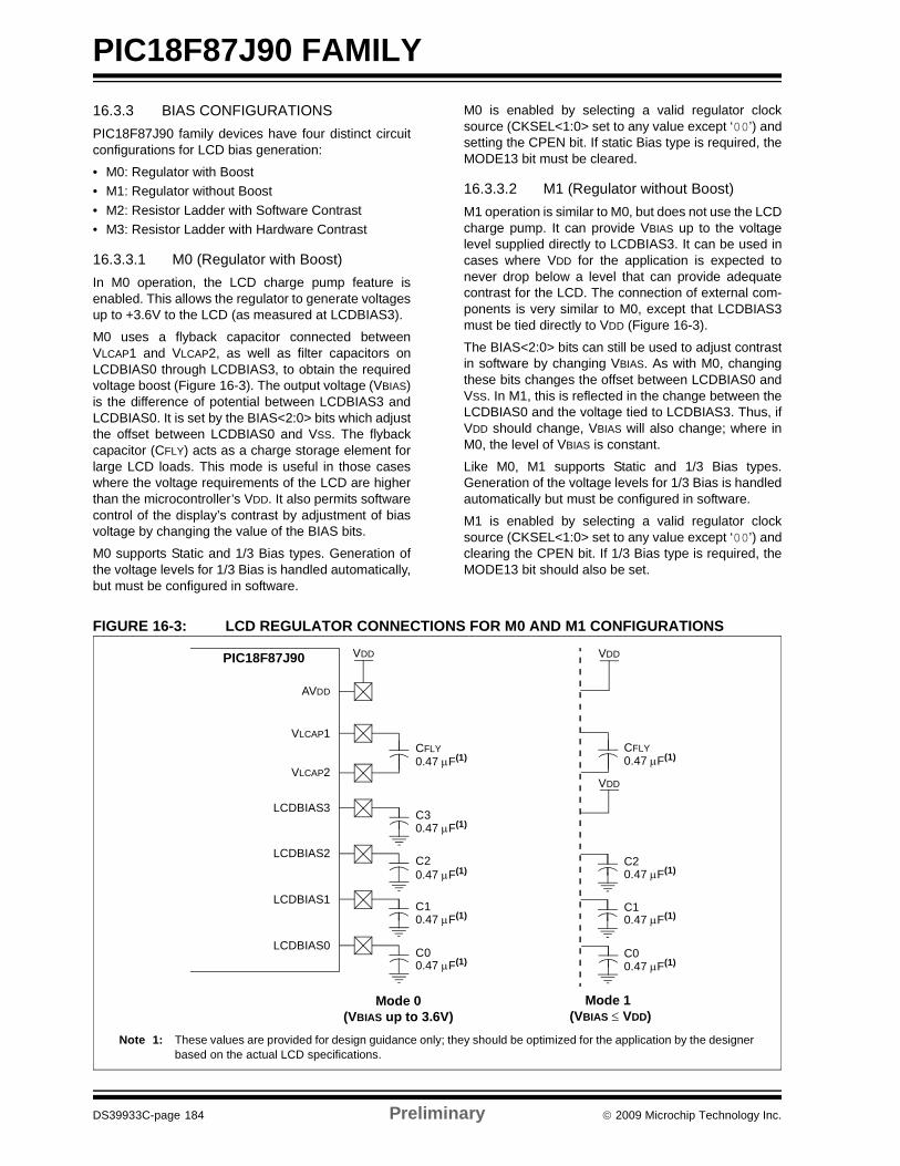
PIC18F87J90 FAMILY
DS39933C-page 184 Preliminary © 2009 Microchip Technology Inc.
16.3.3 BIAS CONFIGURATIONSPIC18F87J90 family devices have four distinct circuitconfigurations for LCD bias generation:
• M0: Regulator with Boost• M1: Regulator without Boost• M2: Resistor Ladder with Software Contrast• M3: Resistor Ladder with Hardware Contrast
16.3.3.1 M0 (Regulator with Boost)In M0 operation, the LCD charge pump feature isenabled. This allows the regulator to generate voltagesup to +3.6V to the LCD (as measured at LCDBIAS3).
M0 uses a flyback capacitor connected betweenVLCAP1 and VLCAP2, as well as filter capacitors onLCDBIAS0 through LCDBIAS3, to obtain the requiredvoltage boost (Figure 16-3). The output voltage (VBIAS)is the difference of potential between LCDBIAS3 andLCDBIAS0. It is set by the BIAS<2:0> bits which adjustthe offset between LCDBIAS0 and VSS. The flybackcapacitor (CFLY) acts as a charge storage element forlarge LCD loads. This mode is useful in those caseswhere the voltage requirements of the LCD are higherthan the microcontroller’s VDD. It also permits softwarecontrol of the display’s contrast by adjustment of biasvoltage by changing the value of the BIAS bits.
M0 supports Static and 1/3 Bias types. Generation ofthe voltage levels for 1/3 Bias is handled automatically,but must be configured in software.
M0 is enabled by selecting a valid regulator clocksource (CKSEL<1:0> set to any value except ‘00’) andsetting the CPEN bit. If static Bias type is required, theMODE13 bit must be cleared.
16.3.3.2 M1 (Regulator without Boost)M1 operation is similar to M0, but does not use the LCDcharge pump. It can provide VBIAS up to the voltagelevel supplied directly to LCDBIAS3. It can be used incases where VDD for the application is expected tonever drop below a level that can provide adequatecontrast for the LCD. The connection of external com-ponents is very similar to M0, except that LCDBIAS3must be tied directly to VDD (Figure 16-3).
The BIAS<2:0> bits can still be used to adjust contrastin software by changing VBIAS. As with M0, changingthese bits changes the offset between LCDBIAS0 andVSS. In M1, this is reflected in the change between theLCDBIAS0 and the voltage tied to LCDBIAS3. Thus, ifVDD should change, VBIAS will also change; where inM0, the level of VBIAS is constant.
Like M0, M1 supports Static and 1/3 Bias types.Generation of the voltage levels for 1/3 Bias is handledautomatically but must be configured in software.
M1 is enabled by selecting a valid regulator clocksource (CKSEL<1:0> set to any value except ‘00’) andclearing the CPEN bit. If 1/3 Bias type is required, theMODE13 bit should also be set.
FIGURE 16-3: LCD REGULATOR CONNECTIONS FOR M0 AND M1 CONFIGURATIONS
LCDBIAS3
LCDBIAS2
LCDBIAS1
LCDBIAS0
AVDD
VDD
VLCAP1
VLCAP2
CFLY
C0
C1
C2
C3
C0
C1
C2
VDD
VDD
(VBIAS up to 3.6V)Mode 0
(VBIAS ≤ VDD)Mode 1
CFLY
Note 1: These values are provided for design guidance only; they should be optimized for the application by the designerbased on the actual LCD specifications.
0.47 μF(1)
0.47 μF(1)
0.47 μF(1)
0.47 μF(1)
0.47 μF(1)
0.47 μF(1)
0.47 μF(1)
0.47 μF(1)
0.47 μF(1)
PIC18F87J90
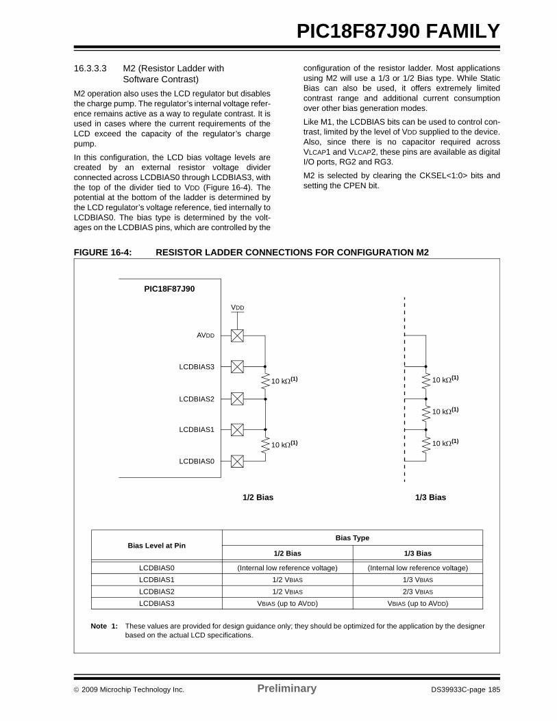
© 2009 Microchip Technology Inc. Preliminary DS39933C-page 185
PIC18F87J90 FAMILY16.3.3.3 M2 (Resistor Ladder with
Software Contrast)M2 operation also uses the LCD regulator but disablesthe charge pump. The regulator’s internal voltage refer-ence remains active as a way to regulate contrast. It isused in cases where the current requirements of theLCD exceed the capacity of the regulator’s chargepump.
In this configuration, the LCD bias voltage levels arecreated by an external resistor voltage dividerconnected across LCDBIAS0 through LCDBIAS3, withthe top of the divider tied to VDD (Figure 16-4). Thepotential at the bottom of the ladder is determined bythe LCD regulator’s voltage reference, tied internally toLCDBIAS0. The bias type is determined by the volt-ages on the LCDBIAS pins, which are controlled by the
configuration of the resistor ladder. Most applicationsusing M2 will use a 1/3 or 1/2 Bias type. While StaticBias can also be used, it offers extremely limitedcontrast range and additional current consumptionover other bias generation modes.
Like M1, the LCDBIAS bits can be used to control con-trast, limited by the level of VDD supplied to the device.Also, since there is no capacitor required acrossVLCAP1 and VLCAP2, these pins are available as digitalI/O ports, RG2 and RG3.
M2 is selected by clearing the CKSEL<1:0> bits andsetting the CPEN bit.
FIGURE 16-4: RESISTOR LADDER CONNECTIONS FOR CONFIGURATION M2
LCDBIAS3
Note 1: These values are provided for design guidance only; they should be optimized for the application by the designerbased on the actual LCD specifications.
Bias Level at PinBias Type
1/2 Bias 1/3 Bias
LCDBIAS0 (Internal low reference voltage) (Internal low reference voltage)LCDBIAS1 1/2 VBIAS 1/3 VBIAS
LCDBIAS2 1/2 VBIAS 2/3 VBIAS
LCDBIAS3 VBIAS (up to AVDD) VBIAS (up to AVDD)
10 kΩ(1)
10 kΩ(1)
1/2 Bias 1/3 Bias
LCDBIAS2
LCDBIAS1
LCDBIAS0
AVDD
10 kΩ(1)
10 kΩ(1)
10 kΩ(1)
VDD
PIC18F87J90
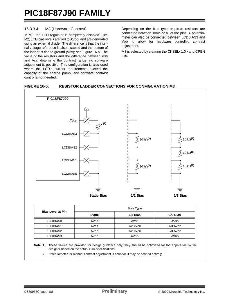
PIC18F87J90 FAMILY
DS39933C-page 186 Preliminary © 2009 Microchip Technology Inc.
16.3.3.4 M3 (Hardware Contrast)In M3, the LCD regulator is completely disabled. LikeM2, LCD bias levels are tied to AVDD, and are generatedusing an external divider. The difference is that the inter-nal voltage reference is also disabled and the bottom ofthe ladder is tied to ground (VSS); see Figure 16-5. Thevalue of the resistors and the difference between VSSand VDD determine the contrast range; no softwareadjustment is possible. This configuration is also usedwhere the LCD’s current requirements exceed thecapacity of the charge pump, and software contrastcontrol is not needed.
Depending on the bias type required, resistors areconnected between some or all of the pins. A potentio-meter can also be connected between LCDBIAS3 andVDD to allow for hardware controlled contrastadjustment.
M3 is selected by clearing the CKSEL<1:0> and CPENbits.
FIGURE 16-5: RESISTOR LADDER CONNECTIONS FOR CONFIGURATION M3
LCDBIAS3
Note 1: These values are provided for design guidance only; they should be optimized for the application by thedesigner based on the actual LCD specifications.
2: Potentiometer for manual contrast adjustment is optional; it may be omitted entirely.
Bias Level at PinBias Type
Static 1/2 Bias 1/3 Bias
LCDBIAS0 AVSS AVSS AVSS
LCDBIAS1 AVSS 1/2 AVDD 1/3 AVDD
LCDBIAS2 AVDD 1/2 AVDD 2/3 AVDD
LCDBIAS3 AVDD AVDD AVDD
10 kΩ(1)
10 kΩ(1)
Static Bias 1/2 Bias 1/3 Bias
LCDBIAS2
LCDBIAS1
LCDBIAS0
AVDD
10 kΩ(1)
10 kΩ(1)
10 kΩ(1)
VDD
(2)
PIC18F87J90
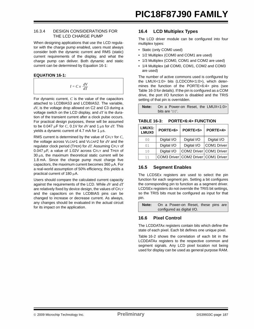
© 2009 Microchip Technology Inc. Preliminary DS39933C-page 187
PIC18F87J90 FAMILY16.3.4 DESIGN CONSIDERATIONS FOR
THE LCD CHARGE PUMPWhen designing applications that use the LCD regula-tor with the charge pump enabled, users must alwaysconsider both the dynamic current and RMS (static)current requirements of the display, and what thecharge pump can deliver. Both dynamic and staticcurrent can be determined by Equation 16-1:
EQUATION 16-1:
For dynamic current, C is the value of the capacitorsattached to LCDBIAS3 and LCDBIAS2. The variable,dV, is the voltage drop allowed on C2 and C3 during avoltage switch on the LCD display, and dT is the dura-tion of the transient current after a clock pulse occurs.For practical design purposes, these will be assumedto be 0.047 μF for C, 0.1V for dV and 1 μs for dT. Thisyields a dynamic current of 4.7 mA for 1 μs.
RMS current is determined by the value of CFLY for C,the voltage across VLCAP1 and VLCAP2 for dV and theregulator clock period (TPER) for dT. Assuming CFLY of0.047 μF, a value of 1.02V across CFLY and TPER of30 μs, the maximum theoretical static current will be1.8 mA. Since the charge pump must charge fivecapacitors, the maximum current becomes 360 μA. Fora real-world assumption of 50% efficiency, this yields apractical current of 180 μA.
Users should compare the calculated current capacityagainst the requirements of the LCD. While dV and dTare relatively fixed by device design, the values of CFLYand the capacitors on the LCDBIAS pins can bechanged to increase or decrease current. As always,any changes should be evaluated in the actual circuitfor its impact on the application.
16.4 LCD Multiplex TypesThe LCD driver module can be configured into fourmultiplex types:
• Static (only COM0 used)• 1/2 Multiplex (COM0 and COM1 are used)• 1/3 Multiplex (COM0, COM1 and COM2 are used)• 1/4 Multiplex (all COM0, COM1, COM2 and COM3
are used)
The number of active commons used is configured bythe LMUX<1:0> bits (LCDCON<1:0>), which deter-mines the function of the PORTE<6:4> pins (seeTable 16-3 for details). If the pin is configured as a COMdrive, the port I/O function is disabled and the TRISsetting of that pin is overridden.
TABLE 16-3: PORTE<6:4> FUNCTION
16.5 Segment EnablesThe LCDSEx registers are used to select the pinfunction for each segment pin. Setting a bit configuresthe corresponding pin to function as a segment driver.LCDSEx registers do not override the TRIS bit settings,so the TRIS bits must be configured as input for thatpin.
16.6 Pixel ControlThe LCDDATAx registers contain bits which define thestate of each pixel. Each bit defines one unique pixel.
Table 16-2 shows the correlation of each bit in theLCDDATAx registers to the respective common andsegment signals. Any LCD pixel location not beingused for display can be used as general purpose RAM.
I = C x dVdT
Note: On a Power-on Reset, the LMUX<1:0>bits are ‘00’.
LMUX1:LMUX0 PORTE<6> PORTE<5> PORTE<4>
00 Digital I/O Digital I/O Digital I/O01 Digital I/O Digital I/O COM1 Driver10 Digital I/O COM2 Driver COM1 Driver11 COM3 Driver COM2 Driver COM1 Driver
Note: On a Power-on Reset, these pins areconfigured as digital I/O.
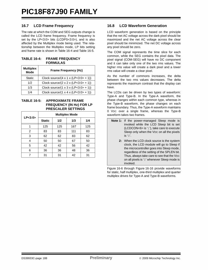
PIC18F87J90 FAMILY
DS39933C-page 188 Preliminary © 2009 Microchip Technology Inc.
16.7 LCD Frame FrequencyThe rate at which the COM and SEG outputs change iscalled the LCD frame frequency. Frame frequency isset by the LP<3:0> bits (LCDPS<3:0>), and is alsoaffected by the Multiplex mode being used. The rela-tionship between the Multiplex mode, LP bits settingand frame rate is shown in Table 16-4 and Table 16-5.
TABLE 16-4: FRAME FREQUENCY FORMULAS
TABLE 16-5: APPROXIMATE FRAME FREQUENCY (IN Hz) FOR LP PRESCALER SETTINGS
16.8 LCD Waveform GenerationLCD waveform generation is based on the principlethat the net AC voltage across the dark pixel should bemaximized and the net AC voltage across the clearpixel should be minimized. The net DC voltage acrossany pixel should be zero.
The COM signal represents the time slice for eachcommon, while the SEG contains the pixel data. Thepixel signal (COM-SEG) will have no DC componentand it can take only one of the two rms values. Thehigher rms value will create a dark pixel and a lowerrms value will create a clear pixel.
As the number of commons increases, the deltabetween the two rms values decreases. The deltarepresents the maximum contrast that the display canhave.
The LCDs can be driven by two types of waveform:Type-A and Type-B. In the Type-A waveform, thephase changes within each common type, whereas inthe Type-B waveform, the phase changes on eachframe boundary. Thus, the Type-A waveform maintains0 VDC over a single frame, whereas the Type-Bwaveform takes two frames.
Figure 16-6 through Figure 16-16 provide waveformsfor static, half multiplex, one-third multiplex and quartermultiplex drives for Type-A and Type-B waveforms.
Multiplex Mode Frame Frequency (Hz)
Static Clock source/(4 x 1 x (LP<3:0> + 1))1/2 Clock source/(2 x 2 x (LP<3:0> + 1))1/3 Clock source/(1 x 3 x (LP<3:0> + 1))1/4 Clock source/(1 x 4 x (LP<3:0> + 1))
LP<3:0>Multiplex Mode
Static 1/2 1/3 1/4
1 125 125 167 1252 83 83 111 833 62 62 83 624 50 50 67 505 42 42 56 426 36 36 48 367 31 31 42 31
Note 1: If the power-managed Sleep mode isinvoked while the LCD Sleep bit is set(LCDCON<6> is ‘1’), take care to executeSleep only when the VDC on all the pixelsis ‘0’.
2: When the LCD clock source is the systemclock, the LCD module will go to Sleep ifthe microcontroller goes into Sleep mode,regardless of the setting of the SPLEN bit.Thus, always take care to see that the VDCon all pixels is ‘0’ whenever Sleep mode isinvoked.
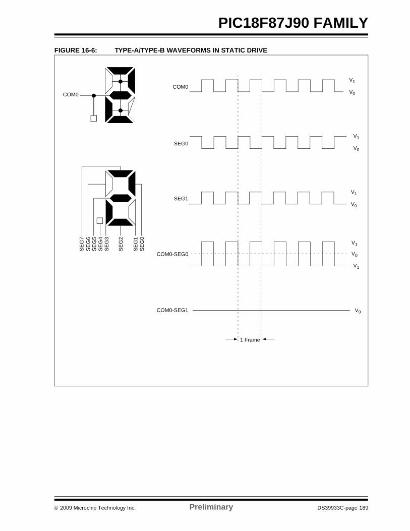
© 2009 Microchip Technology Inc. Preliminary DS39933C-page 189
PIC18F87J90 FAMILYFIGURE 16-6: TYPE-A/TYPE-B WAVEFORMS IN STATIC DRIVE
V1
V0COM0
SEG0
COM0-SEG0
COM0-SEG1
SEG1
V1
V0
V1
V0
V0
V1
-V1
V0
1 Frame
COM0
SE
G0
SE
G1
SE
G2
SE
G3
SE
G4
SE
G5
SE
G6
SE
G7
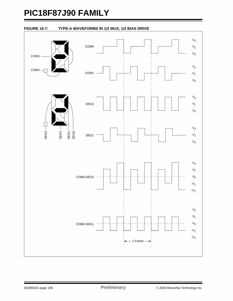
PIC18F87J90 FAMILY
DS39933C-page 190 Preliminary © 2009 Microchip Technology Inc.
FIGURE 16-7: TYPE-A WAVEFORMS IN 1/2 MUX, 1/2 BIAS DRIVE
V2
V1
V0
V2
V1
V0
V2
V1
V0
V2
V1
V0
V2
V1
V0
-V2
-V1
V2
V1
V0
-V2
-V1
COM0
COM1
SEG0
SEG1
COM0-SEG0
COM0-SEG1
1 Frame
COM1
COM0S
EG
0S
EG
1
SE
G2
SE
G3

© 2009 Microchip Technology Inc. Preliminary DS39933C-page 191
PIC18F87J90 FAMILYFIGURE 16-8: TYPE-B WAVEFORMS IN 1/2 MUX, 1/2 BIAS DRIVE
V2
V1
V0
V2
V1
V0
V2
V1
V0
V2
V1
V0
V2
V1
V0
-V2
-V1
V2
V1
V0
-V2
-V1
COM0
COM1
SEG0
SEG1
COM0-SEG0
COM0-SEG1
COM1
COM0
SE
G0
SE
G1
SE
G2
SE
G3
2 Frames

PIC18F87J90 FAMILY
DS39933C-page 192 Preliminary © 2009 Microchip Technology Inc.
FIGURE 16-9: TYPE-A WAVEFORMS IN 1/2 MUX, 1/3 BIAS DRIVE
V3
V2
V1
V0
V3
V2
V1
V0
V3
V2
V1
V0
V3
V2
V1
V0
V3
V2
V1
V0
-V3
-V2
-V1
V3
V2
V1
V0
-V3
-V2
-V1
COM0
COM1
SEG0
SEG1
COM0-SEG0
COM0-SEG1
1 Frame
COM1
COM0S
EG
0S
EG
1
SE
G2
SE
G3
© 2009 Microchip Technology Inc. Preliminary DS39933C-page 193
PIC18F87J90 FAMILYFIGURE 16-10: TYPE-B WAVEFORMS IN 1/2 MUX, 1/3 BIAS DRIVE
V3
V2
V1
V0
V3
V2
V1
V0
V3
V2
V1
V0
V3
V2
V1
V0
V3
V2
V1
V0
-V3
-V2
-V1
V3
V2
V1
V0
-V3
-V2
-V1
COM0
COM1
SEG0
SEG1
COM0-SEG0
COM0-SEG1
COM1
COM0
SEG
0SE
G1
SEG
2
SEG
3
2 Frames
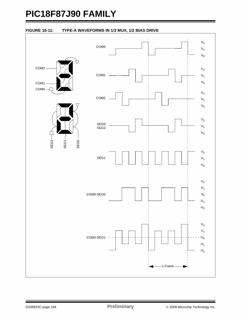
PIC18F87J90 FAMILY
DS39933C-page 194 Preliminary © 2009 Microchip Technology Inc.
FIGURE 16-11: TYPE-A WAVEFORMS IN 1/3 MUX, 1/2 BIAS DRIVE
V2
V1
V0
V2
V1
V0
V2
V1
V0
V2
V1
V0
V2
V1
V0
V2
V1
V0
-V2
-V1
V2
V1
V0
-V2
-V1
COM0
COM1
COM2
SEG0
SEG1
COM0-SEG0
COM0-SEG1
1 Frame
COM2
COM1
COM0
SE
G0
SE
G1
SE
G2
SEG2

© 2009 Microchip Technology Inc. Preliminary DS39933C-page 195
PIC18F87J90 FAMILYFIGURE 16-12: TYPE-B WAVEFORMS IN 1/3 MUX, 1/2 BIAS DRIVE
V2
V1
V0
V2
V1
V0
V2
V1
V0
V2
V1
V0
V2
V1
V0
V2
V1
V0
-V2
-V1
V2
V1
V0
-V2
-V1
COM0
COM1
COM2
SEG0
SEG1
COM0-SEG0
COM0-SEG1
2 Frames
COM2
COM1
COM0S
EG
0
SE
G1
SE
G2
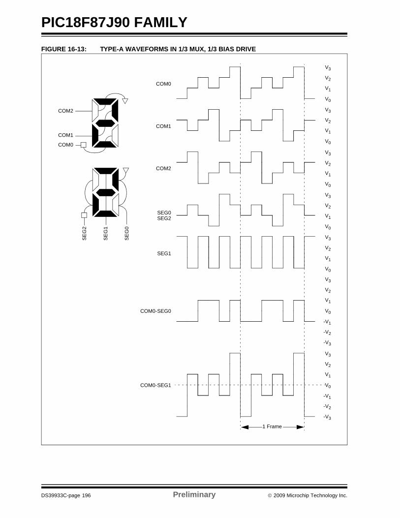
PIC18F87J90 FAMILY
DS39933C-page 196 Preliminary © 2009 Microchip Technology Inc.
FIGURE 16-13: TYPE-A WAVEFORMS IN 1/3 MUX, 1/3 BIAS DRIVE
V3
V2
V1
V0
V3
V2
V1
V0
V3
V2
V1
V0
V3
V2
V1
V0
V3
V2
V1
V0
V3
V2
V1
V0
-V3
-V2
-V1
V3
V2
V1
V0
-V3
-V2
-V1
COM0
COM1
COM2
SEG0
SEG1
COM0-SEG0
COM0-SEG1
1 Frame
COM2
COM1
COM0
SE
G0
SE
G1
SE
G2
SEG2
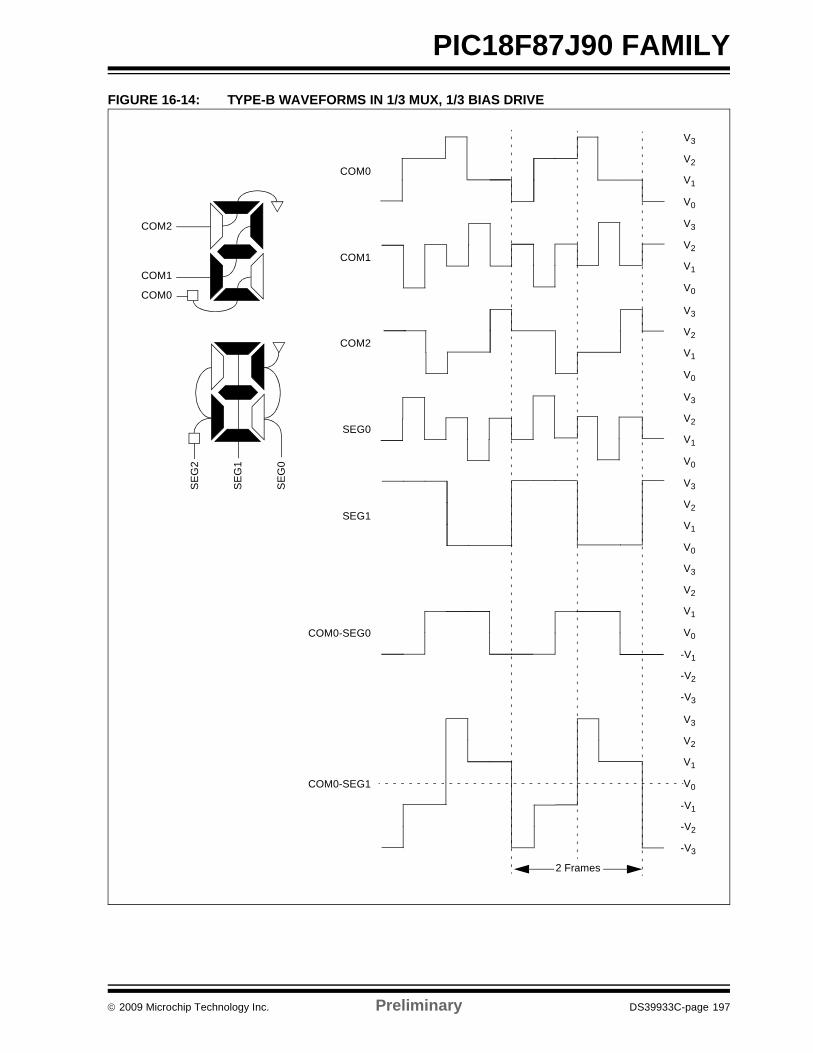
© 2009 Microchip Technology Inc. Preliminary DS39933C-page 197
PIC18F87J90 FAMILYFIGURE 16-14: TYPE-B WAVEFORMS IN 1/3 MUX, 1/3 BIAS DRIVE
V3
V2
V1
V0
V3
V2
V1
V0
V3
V2
V1
V0
V3
V2
V1
V0
V3
V2
V1
V0
V3
V2
V1
V0
-V3
-V2
-V1
V3
V2
V1
V0
-V3
-V2
-V1
COM0
COM1
COM2
SEG0
SEG1
COM0-SEG0
COM0-SEG1
2 Frames
COM2
COM1
COM0S
EG
0
SE
G1
SE
G2
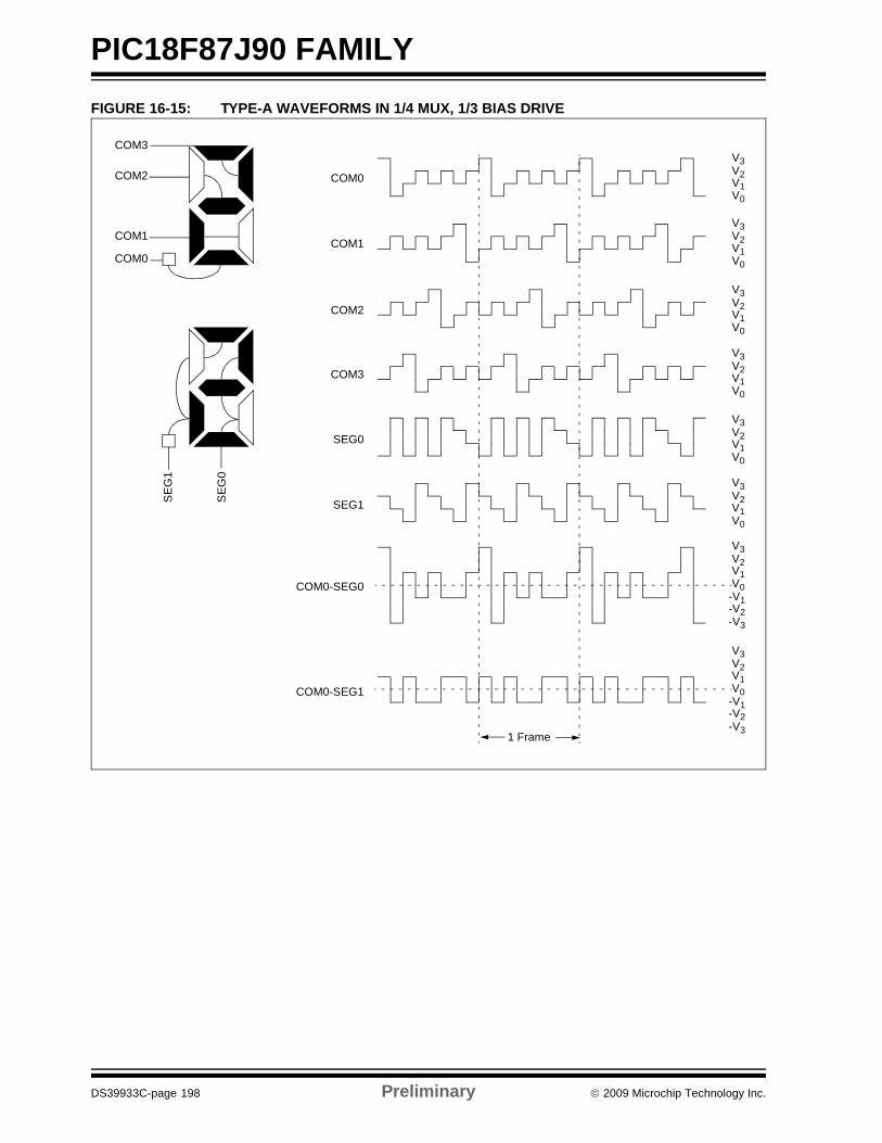
PIC18F87J90 FAMILY
DS39933C-page 198 Preliminary © 2009 Microchip Technology Inc.
FIGURE 16-15: TYPE-A WAVEFORMS IN 1/4 MUX, 1/3 BIAS DRIVE
V3V2V1V0
V3V2V1V0
V3V2V1V0
V3V2V1V0
V3V2V1V0
V3V2V1V0
V3V2V1V0
-V3
-V2-V1
V3V2V1V0
-V3
-V2-V1
COM0
COM1
COM2
COM3
SEG0
SEG1
COM0-SEG0
COM0-SEG1
COM3
COM2
COM1
COM0
1 Frame
SE
G0
SE
G1
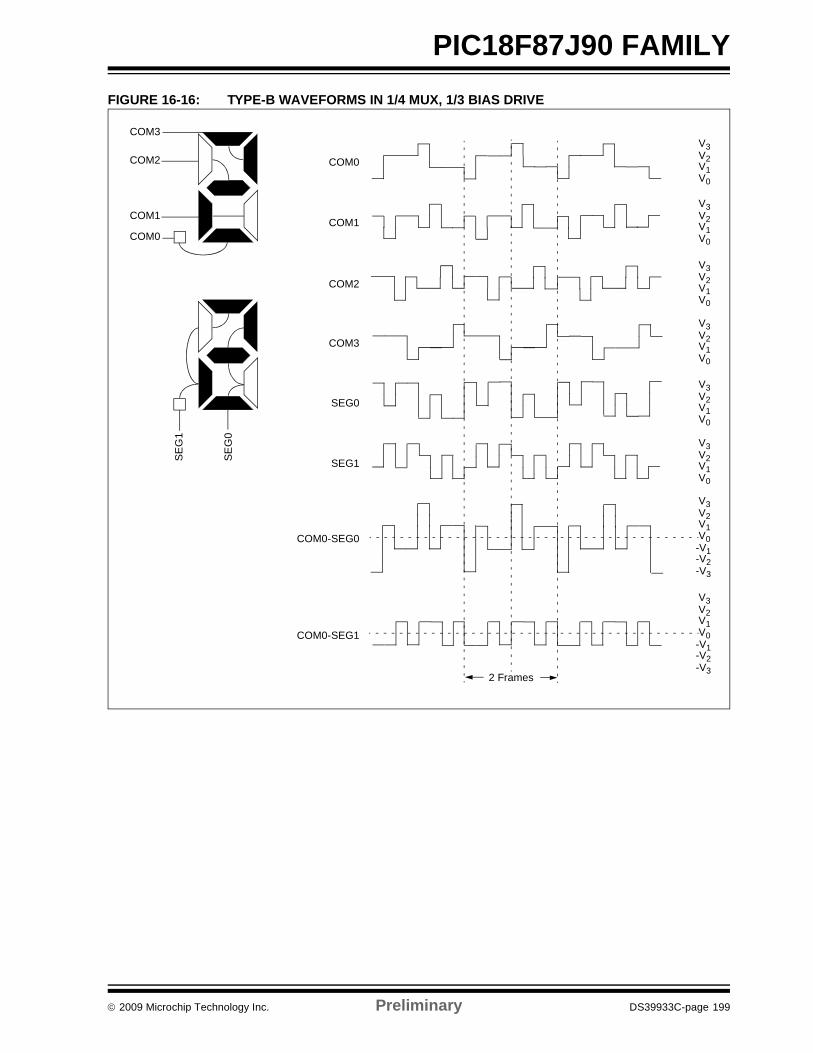
© 2009 Microchip Technology Inc. Preliminary DS39933C-page 199
PIC18F87J90 FAMILYFIGURE 16-16: TYPE-B WAVEFORMS IN 1/4 MUX, 1/3 BIAS DRIVE
V3V2V1V0
V3V2V1V0
V3V2V1V0
V3V2V1V0
V3V2V1V0
V3V2V1V0
V3V2V1V0
-V3
-V2-V1
V3V2V1V0
-V3
-V2-V1
COM0
COM1
COM2
COM3
SEG0
SEG1
COM0-SEG0
COM0-SEG1
COM3
COM2
COM1
COM0
2 Frames
SE
G0
SE
G1
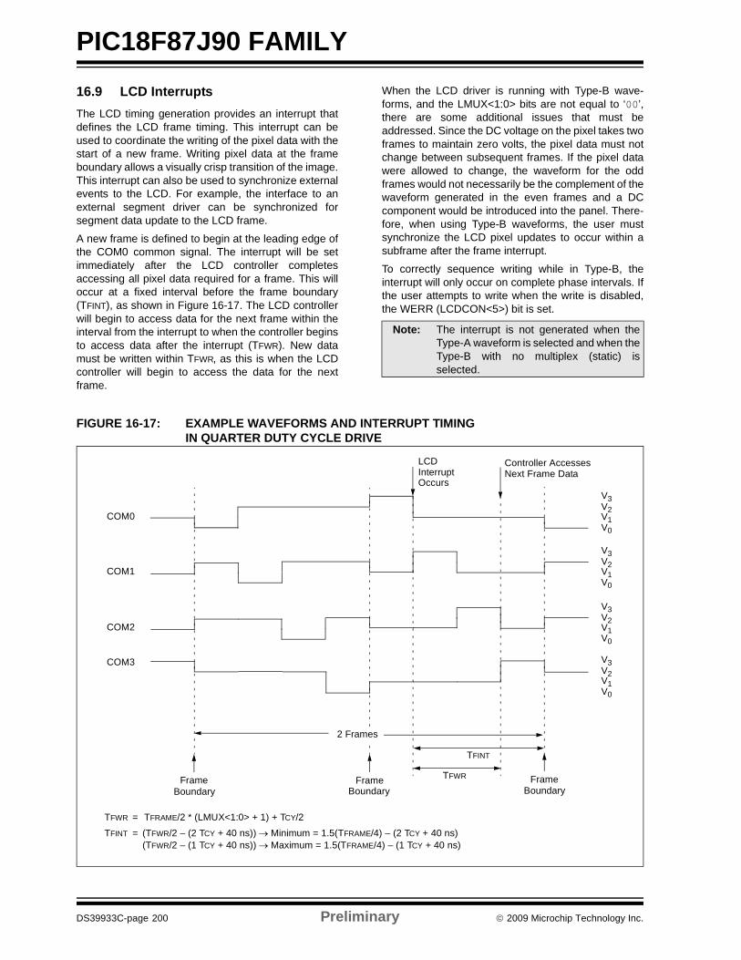
PIC18F87J90 FAMILY
DS39933C-page 200 Preliminary © 2009 Microchip Technology Inc.
16.9 LCD InterruptsThe LCD timing generation provides an interrupt thatdefines the LCD frame timing. This interrupt can beused to coordinate the writing of the pixel data with thestart of a new frame. Writing pixel data at the frameboundary allows a visually crisp transition of the image.This interrupt can also be used to synchronize externalevents to the LCD. For example, the interface to anexternal segment driver can be synchronized forsegment data update to the LCD frame.
A new frame is defined to begin at the leading edge ofthe COM0 common signal. The interrupt will be setimmediately after the LCD controller completesaccessing all pixel data required for a frame. This willoccur at a fixed interval before the frame boundary(TFINT), as shown in Figure 16-17. The LCD controllerwill begin to access data for the next frame within theinterval from the interrupt to when the controller beginsto access data after the interrupt (TFWR). New datamust be written within TFWR, as this is when the LCDcontroller will begin to access the data for the nextframe.
When the LCD driver is running with Type-B wave-forms, and the LMUX<1:0> bits are not equal to ‘00’,there are some additional issues that must beaddressed. Since the DC voltage on the pixel takes twoframes to maintain zero volts, the pixel data must notchange between subsequent frames. If the pixel datawere allowed to change, the waveform for the oddframes would not necessarily be the complement of thewaveform generated in the even frames and a DCcomponent would be introduced into the panel. There-fore, when using Type-B waveforms, the user mustsynchronize the LCD pixel updates to occur within asubframe after the frame interrupt.
To correctly sequence writing while in Type-B, theinterrupt will only occur on complete phase intervals. Ifthe user attempts to write when the write is disabled,the WERR (LCDCON<5>) bit is set.
FIGURE 16-17: EXAMPLE WAVEFORMS AND INTERRUPT TIMING IN QUARTER DUTY CYCLE DRIVE
Note: The interrupt is not generated when theType-A waveform is selected and when theType-B with no multiplex (static) isselected.
FrameBoundary
FrameBoundary
LCDInterruptOccurs
Controller AccessesNext Frame Data
TFINT
TFWR
TFWR = TFRAME/2 * (LMUX<1:0> + 1) + TCY/2TFINT = (TFWR/2 – (2 TCY + 40 ns)) → Minimum = 1.5(TFRAME/4) – (2 TCY + 40 ns)
(TFWR/2 – (1 TCY + 40 ns)) → Maximum = 1.5(TFRAME/4) – (1 TCY + 40 ns)
FrameBoundary
V3V2V1V0
V3V2V1V0
V3V2V1V0
V3V2V1V0
COM0
COM1
COM2
COM3
2 Frames
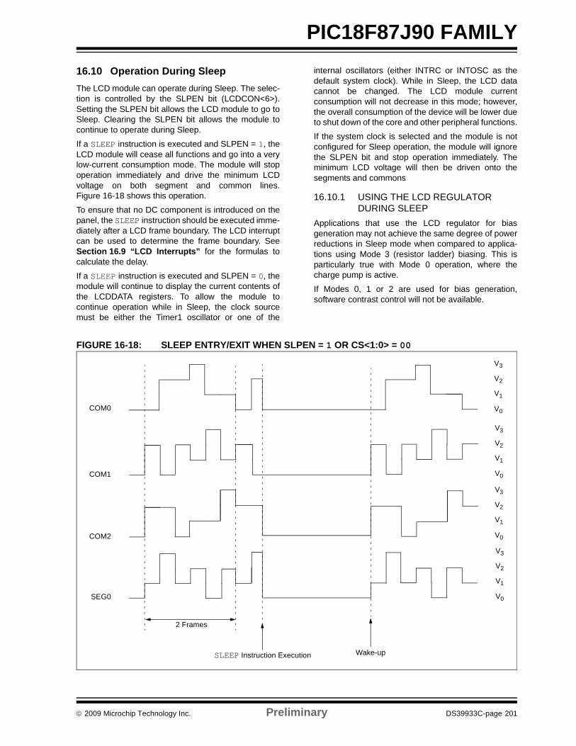
© 2009 Microchip Technology Inc. Preliminary DS39933C-page 201
PIC18F87J90 FAMILY16.10 Operation During SleepThe LCD module can operate during Sleep. The selec-tion is controlled by the SLPEN bit (LCDCON<6>).Setting the SLPEN bit allows the LCD module to go toSleep. Clearing the SLPEN bit allows the module tocontinue to operate during Sleep.
If a SLEEP instruction is executed and SLPEN = 1, theLCD module will cease all functions and go into a verylow-current consumption mode. The module will stopoperation immediately and drive the minimum LCDvoltage on both segment and common lines.Figure 16-18 shows this operation.
To ensure that no DC component is introduced on thepanel, the SLEEP instruction should be executed imme-diately after a LCD frame boundary. The LCD interruptcan be used to determine the frame boundary. SeeSection 16.9 “LCD Interrupts” for the formulas tocalculate the delay.
If a SLEEP instruction is executed and SLPEN = 0, themodule will continue to display the current contents ofthe LCDDATA registers. To allow the module tocontinue operation while in Sleep, the clock sourcemust be either the Timer1 oscillator or one of the
internal oscillators (either INTRC or INTOSC as thedefault system clock). While in Sleep, the LCD datacannot be changed. The LCD module currentconsumption will not decrease in this mode; however,the overall consumption of the device will be lower dueto shut down of the core and other peripheral functions.
If the system clock is selected and the module is notconfigured for Sleep operation, the module will ignorethe SLPEN bit and stop operation immediately. Theminimum LCD voltage will then be driven onto thesegments and commons
16.10.1 USING THE LCD REGULATOR DURING SLEEP
Applications that use the LCD regulator for biasgeneration may not achieve the same degree of powerreductions in Sleep mode when compared to applica-tions using Mode 3 (resistor ladder) biasing. This isparticularly true with Mode 0 operation, where thecharge pump is active.
If Modes 0, 1 or 2 are used for bias generation,software contrast control will not be available.
FIGURE 16-18: SLEEP ENTRY/EXIT WHEN SLPEN = 1 OR CS<1:0> = 00
SLEEP Instruction Execution Wake-up
2 Frames
V3
V2
V1
V0
V3
V2
V1
V0
V3
V2
V1
V0
V3
V2
V1
V0
COM0
COM1
COM2
SEG0
PIC18F87J90 FAMILY
DS39933C-page 202 Preliminary © 2009 Microchip Technology Inc.
16.11 Configuring the LCD ModuleThe following is the sequence of steps to configure theLCD module.
1. Select the frame clock prescale using bits,LP<3:0> (LCDPS<3:0>).
2. Configure the appropriate pins to function assegment drivers using the LCDSEx registers.
3. Configure the appropriate pins as inputs usingTRISx registers.
4. Configure the LCD module for the followingusing the LCDCON register:• Multiplex and Bias mode (LMUX<1:0>)• Timing source (CS<1:0>)• Sleep mode (SLPEN)
5. Write initial values to pixel data registers,LCDDATA0 through LCDDATA23.
6. Configure the LCD regulator:a) If M2 or M3 bias configuration is to be used,
turn off the regulator by settingCKSEL<1:0> (LCDREG<1:0>) to ‘00’. Setor clear the CPEN bit (LCDREG<6>) toselect Mode 2 or Mode 3, as appropriate.
b) If M0 or M1 bias generation is to be used:• Set the VBIAS level using the BIAS<2:0>
bits (LCDREG<5:3>).• Set or clear the CPEN bit to enable or
disable the charge pump.• Set or clear the MODE13 bit
(LCDREG<2>) to select the Bias mode.• Select a regulator clock source using the
CKSEL<1:0> bits.7. Clear LCD Interrupt Flag, LCDIF (PIR3<6>),
and if desired, enable the interrupt by setting theLCDIE bit (PIE3<6>).
8. Enable the LCD module by setting the LCDENbit (LCDCON<7>).
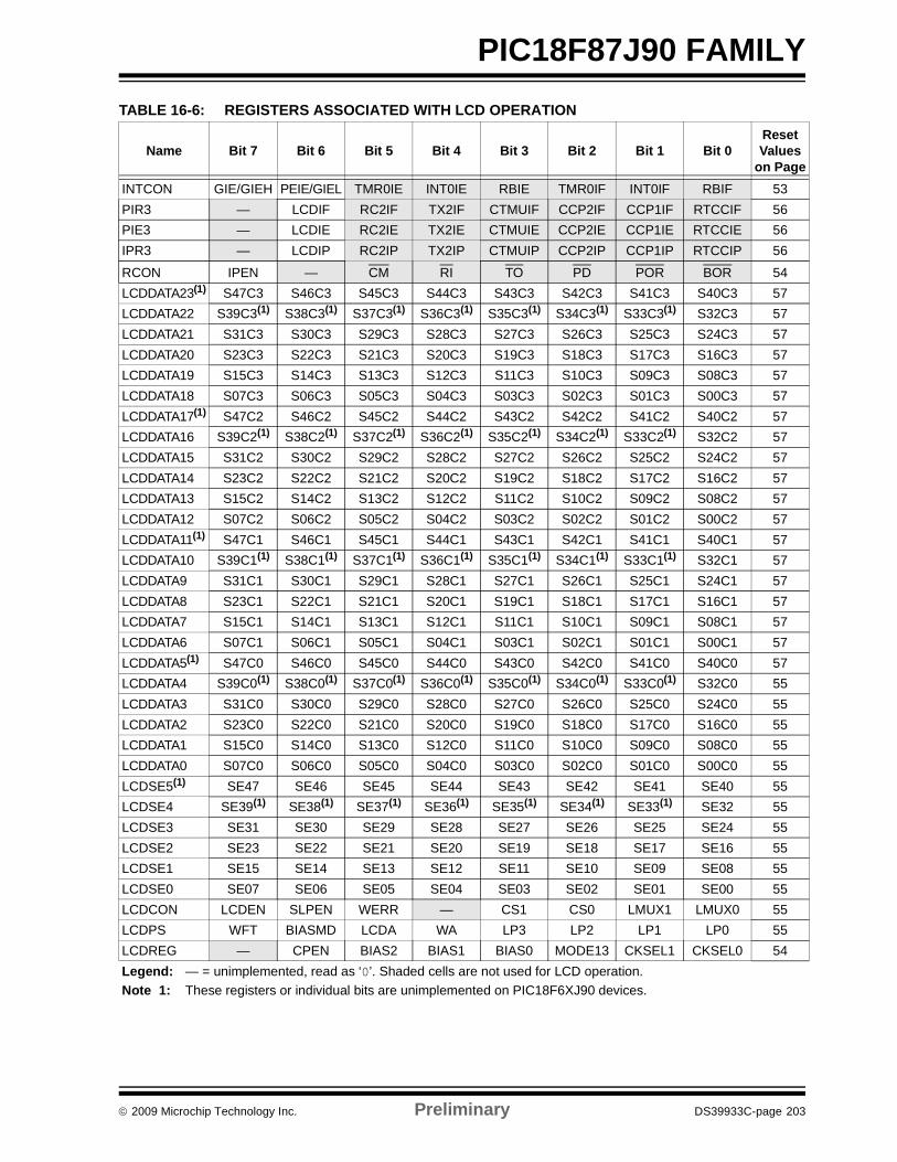
© 2009 Microchip Technology Inc. Preliminary DS39933C-page 203
PIC18F87J90 FAMILYTABLE 16-6: REGISTERS ASSOCIATED WITH LCD OPERATION
Name Bit 7 Bit 6 Bit 5 Bit 4 Bit 3 Bit 2 Bit 1 Bit 0Reset Values
on PageINTCON GIE/GIEH PEIE/GIEL TMR0IE INT0IE RBIE TMR0IF INT0IF RBIF 53PIR3 — LCDIF RC2IF TX2IF CTMUIF CCP2IF CCP1IF RTCCIF 56PIE3 — LCDIE RC2IE TX2IE CTMUIE CCP2IE CCP1IE RTCCIE 56IPR3 — LCDIP RC2IP TX2IP CTMUIP CCP2IP CCP1IP RTCCIP 56
RCON IPEN — CM RI TO PD POR BOR 54LCDDATA23(1) S47C3 S46C3 S45C3 S44C3 S43C3 S42C3 S41C3 S40C3 57LCDDATA22 S39C3(1) S38C3(1) S37C3(1) S36C3(1) S35C3(1) S34C3(1) S33C3(1) S32C3 57LCDDATA21 S31C3 S30C3 S29C3 S28C3 S27C3 S26C3 S25C3 S24C3 57LCDDATA20 S23C3 S22C3 S21C3 S20C3 S19C3 S18C3 S17C3 S16C3 57LCDDATA19 S15C3 S14C3 S13C3 S12C3 S11C3 S10C3 S09C3 S08C3 57LCDDATA18 S07C3 S06C3 S05C3 S04C3 S03C3 S02C3 S01C3 S00C3 57LCDDATA17(1) S47C2 S46C2 S45C2 S44C2 S43C2 S42C2 S41C2 S40C2 57LCDDATA16 S39C2(1) S38C2(1) S37C2(1) S36C2(1) S35C2(1) S34C2(1) S33C2(1) S32C2 57LCDDATA15 S31C2 S30C2 S29C2 S28C2 S27C2 S26C2 S25C2 S24C2 57LCDDATA14 S23C2 S22C2 S21C2 S20C2 S19C2 S18C2 S17C2 S16C2 57LCDDATA13 S15C2 S14C2 S13C2 S12C2 S11C2 S10C2 S09C2 S08C2 57LCDDATA12 S07C2 S06C2 S05C2 S04C2 S03C2 S02C2 S01C2 S00C2 57LCDDATA11(1) S47C1 S46C1 S45C1 S44C1 S43C1 S42C1 S41C1 S40C1 57LCDDATA10 S39C1(1) S38C1(1) S37C1(1) S36C1(1) S35C1(1) S34C1(1) S33C1(1) S32C1 57LCDDATA9 S31C1 S30C1 S29C1 S28C1 S27C1 S26C1 S25C1 S24C1 57LCDDATA8 S23C1 S22C1 S21C1 S20C1 S19C1 S18C1 S17C1 S16C1 57LCDDATA7 S15C1 S14C1 S13C1 S12C1 S11C1 S10C1 S09C1 S08C1 57LCDDATA6 S07C1 S06C1 S05C1 S04C1 S03C1 S02C1 S01C1 S00C1 57LCDDATA5(1) S47C0 S46C0 S45C0 S44C0 S43C0 S42C0 S41C0 S40C0 57LCDDATA4 S39C0(1) S38C0(1) S37C0(1) S36C0(1) S35C0(1) S34C0(1) S33C0(1) S32C0 55LCDDATA3 S31C0 S30C0 S29C0 S28C0 S27C0 S26C0 S25C0 S24C0 55LCDDATA2 S23C0 S22C0 S21C0 S20C0 S19C0 S18C0 S17C0 S16C0 55LCDDATA1 S15C0 S14C0 S13C0 S12C0 S11C0 S10C0 S09C0 S08C0 55LCDDATA0 S07C0 S06C0 S05C0 S04C0 S03C0 S02C0 S01C0 S00C0 55LCDSE5(1) SE47 SE46 SE45 SE44 SE43 SE42 SE41 SE40 55LCDSE4 SE39(1) SE38(1) SE37(1) SE36(1) SE35(1) SE34(1) SE33(1) SE32 55LCDSE3 SE31 SE30 SE29 SE28 SE27 SE26 SE25 SE24 55LCDSE2 SE23 SE22 SE21 SE20 SE19 SE18 SE17 SE16 55LCDSE1 SE15 SE14 SE13 SE12 SE11 SE10 SE09 SE08 55LCDSE0 SE07 SE06 SE05 SE04 SE03 SE02 SE01 SE00 55LCDCON LCDEN SLPEN WERR — CS1 CS0 LMUX1 LMUX0 55LCDPS WFT BIASMD LCDA WA LP3 LP2 LP1 LP0 55LCDREG — CPEN BIAS2 BIAS1 BIAS0 MODE13 CKSEL1 CKSEL0 54Legend: — = unimplemented, read as ‘0’. Shaded cells are not used for LCD operation.Note 1: These registers or individual bits are unimplemented on PIC18F6XJ90 devices.

PIC18F87J90 FAMILY
DS39933C-page 204 Preliminary © 2009 Microchip Technology Inc.
NOTES:
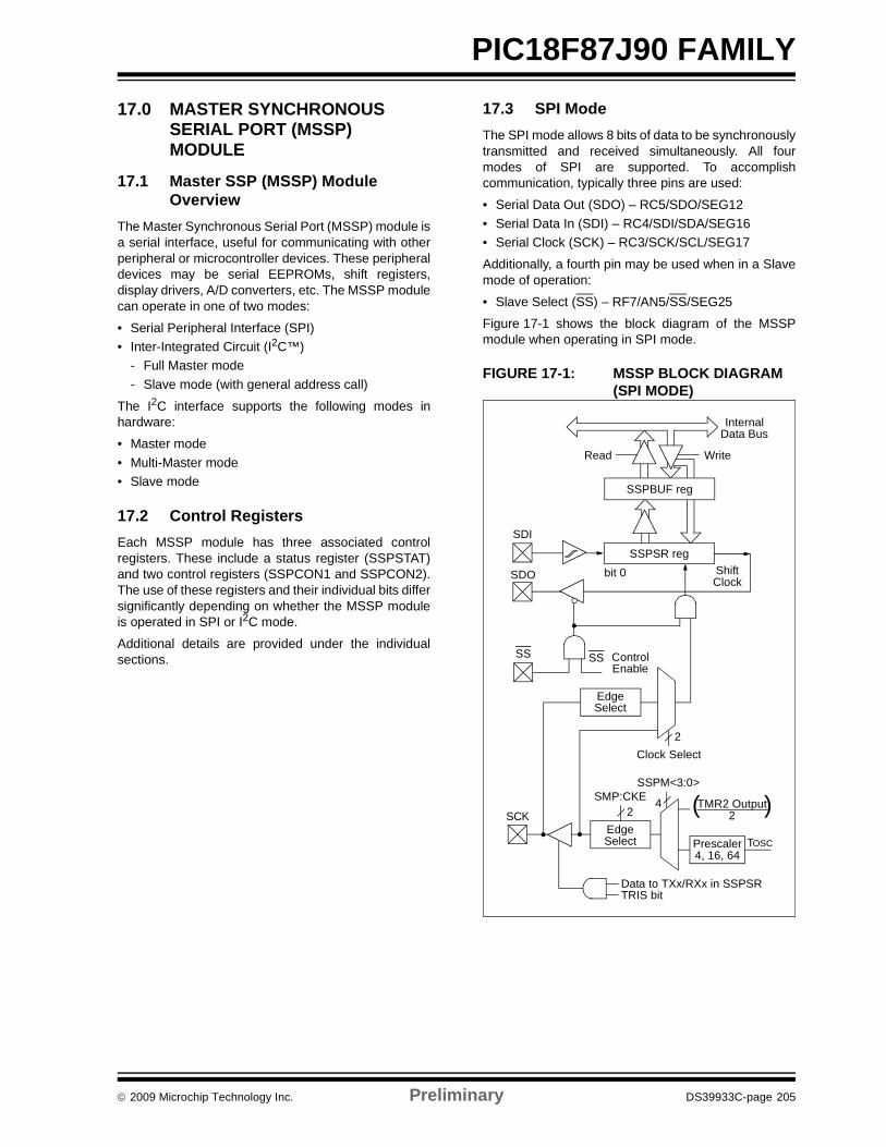
© 2009 Microchip Technology Inc. Preliminary DS39933C-page 205
PIC18F87J90 FAMILY17.0 MASTER SYNCHRONOUS
SERIAL PORT (MSSP) MODULE
17.1 Master SSP (MSSP) Module Overview
The Master Synchronous Serial Port (MSSP) module isa serial interface, useful for communicating with otherperipheral or microcontroller devices. These peripheraldevices may be serial EEPROMs, shift registers,display drivers, A/D converters, etc. The MSSP modulecan operate in one of two modes:
• Serial Peripheral Interface (SPI)• Inter-Integrated Circuit (I2C™)
- Full Master mode- Slave mode (with general address call)
The I2C interface supports the following modes inhardware:
• Master mode• Multi-Master mode• Slave mode
17.2 Control RegistersEach MSSP module has three associated controlregisters. These include a status register (SSPSTAT)and two control registers (SSPCON1 and SSPCON2).The use of these registers and their individual bits differsignificantly depending on whether the MSSP moduleis operated in SPI or I2C mode.
Additional details are provided under the individualsections.
17.3 SPI ModeThe SPI mode allows 8 bits of data to be synchronouslytransmitted and received simultaneously. All fourmodes of SPI are supported. To accomplishcommunication, typically three pins are used:
• Serial Data Out (SDO) – RC5/SDO/SEG12• Serial Data In (SDI) – RC4/SDI/SDA/SEG16• Serial Clock (SCK) – RC3/SCK/SCL/SEG17
Additionally, a fourth pin may be used when in a Slavemode of operation:
• Slave Select (SS) – RF7/AN5/SS/SEG25
Figure 17-1 shows the block diagram of the MSSPmodule when operating in SPI mode.
FIGURE 17-1: MSSP BLOCK DIAGRAM (SPI MODE)
( )
Read Write
InternalData Bus
SSPSR reg
SSPM<3:0>
bit 0 ShiftClock
SS ControlEnable
EdgeSelect
Clock Select
TMR2 Output
TOSCPrescaler4, 16, 64
2EdgeSelect
2
4
Data to TXx/RXx in SSPSRTRIS bit
2SMP:CKE
SDO
SSPBUF reg
SDI
SS
SCK
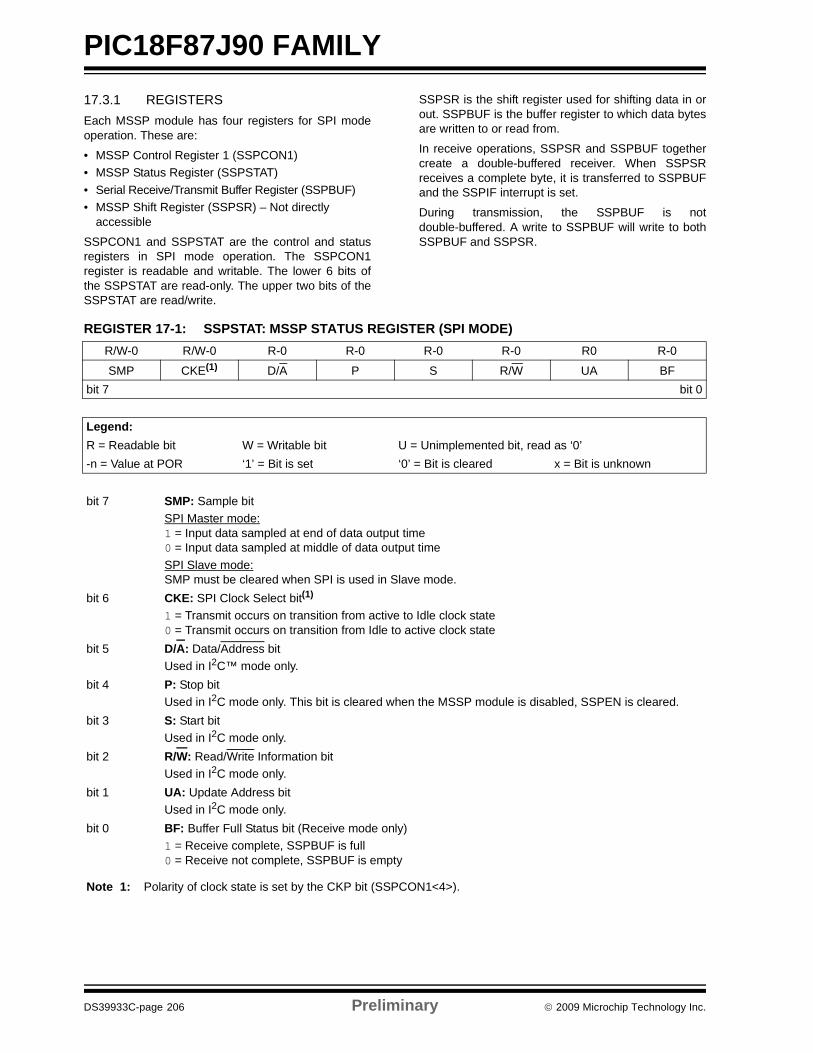
PIC18F87J90 FAMILY
DS39933C-page 206 Preliminary © 2009 Microchip Technology Inc.
17.3.1 REGISTERSEach MSSP module has four registers for SPI modeoperation. These are:
• MSSP Control Register 1 (SSPCON1)• MSSP Status Register (SSPSTAT)• Serial Receive/Transmit Buffer Register (SSPBUF)• MSSP Shift Register (SSPSR) – Not directly
accessible
SSPCON1 and SSPSTAT are the control and statusregisters in SPI mode operation. The SSPCON1register is readable and writable. The lower 6 bits ofthe SSPSTAT are read-only. The upper two bits of theSSPSTAT are read/write.
SSPSR is the shift register used for shifting data in orout. SSPBUF is the buffer register to which data bytesare written to or read from.
In receive operations, SSPSR and SSPBUF togethercreate a double-buffered receiver. When SSPSRreceives a complete byte, it is transferred to SSPBUFand the SSPIF interrupt is set.
During transmission, the SSPBUF is notdouble-buffered. A write to SSPBUF will write to bothSSPBUF and SSPSR.
REGISTER 17-1: SSPSTAT: MSSP STATUS REGISTER (SPI MODE)R/W-0 R/W-0 R-0 R-0 R-0 R-0 R0 R-0
SMP CKE(1) D/A P S R/W UA BFbit 7 bit 0
Legend:R = Readable bit W = Writable bit U = Unimplemented bit, read as ‘0’-n = Value at POR ‘1’ = Bit is set ‘0’ = Bit is cleared x = Bit is unknown
bit 7 SMP: Sample bitSPI Master mode:1 = Input data sampled at end of data output time0 = Input data sampled at middle of data output timeSPI Slave mode:SMP must be cleared when SPI is used in Slave mode.
bit 6 CKE: SPI Clock Select bit(1)
1 = Transmit occurs on transition from active to Idle clock state0 = Transmit occurs on transition from Idle to active clock state
bit 5 D/A: Data/Address bit Used in I2C™ mode only.
bit 4 P: Stop bit Used in I2C mode only. This bit is cleared when the MSSP module is disabled, SSPEN is cleared.
bit 3 S: Start bitUsed in I2C mode only.
bit 2 R/W: Read/Write Information bitUsed in I2C mode only.
bit 1 UA: Update Address bitUsed in I2C mode only.
bit 0 BF: Buffer Full Status bit (Receive mode only)1 = Receive complete, SSPBUF is full 0 = Receive not complete, SSPBUF is empty
Note 1: Polarity of clock state is set by the CKP bit (SSPCON1<4>).
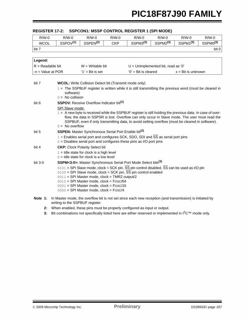
© 2009 Microchip Technology Inc. Preliminary DS39933C-page 207
PIC18F87J90 FAMILY
REGISTER 17-2: SSPCON1: MSSP CONTROL REGISTER 1 (SPI MODE)R/W-0 R/W-0 R/W-0 R/W-0 R/W-0 R/W-0 R/W-0 R/W-0WCOL SSPOV(1) SSPEN(2) CKP SSPM3(3) SSPM2(3) SSPM1(3) SSPM0(3)
bit 7 bit 0
Legend:R = Readable bit W = Writable bit U = Unimplemented bit, read as ‘0’-n = Value at POR ‘1’ = Bit is set ‘0’ = Bit is cleared x = Bit is unknown
bit 7 WCOL: Write Collision Detect bit (Transmit mode only)1 = The SSPBUF register is written while it is still transmitting the previous word (must be cleared in
software) 0 = No collision
bit 6 SSPOV: Receive Overflow Indicator bit(1) SPI Slave mode: 1 = A new byte is received while the SSPBUF register is still holding the previous data. In case of over-
flow, the data in SSPSR is lost. Overflow can only occur in Slave mode. The user must read theSSPBUF, even if only transmitting data, to avoid setting overflow (must be cleared in software).
0 = No overflowbit 5 SSPEN: Master Synchronous Serial Port Enable bit(2)
1 = Enables serial port and configures SCK, SDO, SDI and SS as serial port pins 0 = Disables serial port and configures these pins as I/O port pins
bit 4 CKP: Clock Polarity Select bit 1 = Idle state for clock is a high level 0 = Idle state for clock is a low level
bit 3-0 SSPM<3:0>: Master Synchronous Serial Port Mode Select bits(3)
0101 = SPI Slave mode, clock = SCK pin, SS pin control disabled, SS can be used as I/O pin0100 = SPI Slave mode, clock = SCK pin, SS pin control enabled0011 = SPI Master mode, clock = TMR2 output/2 0010 = SPI Master mode, clock = FOSC/64 0001 = SPI Master mode, clock = FOSC/16 0000 = SPI Master mode, clock = FOSC/4
Note 1: In Master mode, the overflow bit is not set since each new reception (and transmission) is initiated by writing to the SSPBUF register.
2: When enabled, these pins must be properly configured as input or output.3: Bit combinations not specifically listed here are either reserved or implemented in I2C™ mode only.
PIC18F87J90 FAMILY
DS39933C-page 208 Preliminary © 2009 Microchip Technology Inc.
17.3.2 OPERATIONWhen initializing the SPI, several options need to bespecified. This is done by programming the appropriatecontrol bits (SSPCON1<5:0> and SSPSTAT<7:6>).These control bits allow the following to be specified:
• Master mode (SCK is the clock output)• Slave mode (SCK is the clock input)• Clock Polarity (Idle state of SCK)• Data Input Sample Phase (middle or end of data
output time)• Clock Edge (output data on rising/falling edge of
SCK)• Clock Rate (Master mode only)• Slave Select mode (Slave mode only)
Each MSSP consists of a transmit/receive shift register(SSPSR) and a buffer register (SSPBUF). The SSPSRshifts the data in and out of the device, MSb first. TheSSPBUF holds the data that was written to the SSPSRuntil the received data is ready. Once the 8 bits of datahave been received, that byte is moved to the SSPBUFregister. Then, the Buffer Full detect bit, BF(SSPSTAT<0>), and the interrupt flag bit, SSPIF, areset. This double-buffering of the received data(SSPBUF) allows the next byte to start reception before
reading the data that was just received. Any write to theSSPBUF register during transmission/reception of datawill be ignored and the Write Collision detect bit, WCOL(SSPCON1<7>), will be set. User software must clearthe WCOL bit so that it can be determined if the follow-ing write(s) to the SSPBUF register completedsuccessfully.
When the application software is expecting to receivevalid data, the SSPBUF should be read before the nextbyte of data to transfer is written to the SSPBUF. TheBuffer Full bit, BF (SSPSTAT<0>), indicates whenSSPBUF has been loaded with the received data (trans-mission is complete). When the SSPBUF is read, the BFbit is cleared. This data may be irrelevant if the SPI isonly a transmitter. Generally, the MSSP interrupt is usedto determine when the transmission/reception has com-pleted. The SSPBUF must be read and/or written. If theinterrupt method is not going to be used, then softwarepolling can be done to ensure that a write collision doesnot occur. Example 17-1 shows the loading of theSSPBUF (SSPSR) for data transmission.
The SSPSR is not directly readable or writable and canonly be accessed by addressing the SSPBUF register.Additionally, the SSPSTAT register indicates thevarious status conditions.
EXAMPLE 17-1: LOADING THE SSPBUF (SSPSR) REGISTERLOOP BTFSS SSPSTAT, BF ;Has data been received (transmit complete)?
BRA LOOP ;No MOVF SSPBUF, W ;WREG reg = contents of SSPBUFMOVWF RXDATA ;Save in user RAM, if data is meaningfulMOVF TXDATA, W ;W reg = contents of TXDATA MOVWF SSPBUF ;New data to xmit
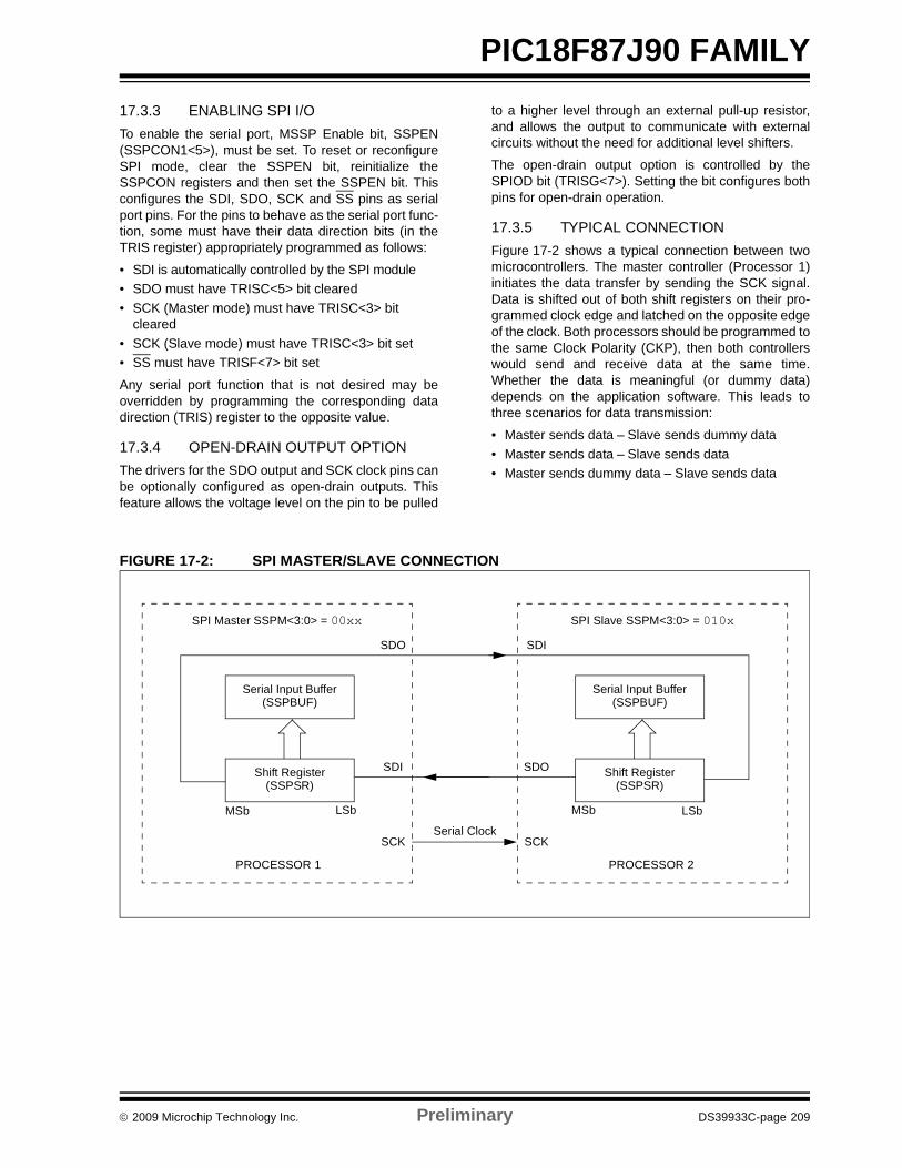
© 2009 Microchip Technology Inc. Preliminary DS39933C-page 209
PIC18F87J90 FAMILY17.3.3 ENABLING SPI I/OTo enable the serial port, MSSP Enable bit, SSPEN(SSPCON1<5>), must be set. To reset or reconfigureSPI mode, clear the SSPEN bit, reinitialize theSSPCON registers and then set the SSPEN bit. Thisconfigures the SDI, SDO, SCK and SS pins as serialport pins. For the pins to behave as the serial port func-tion, some must have their data direction bits (in theTRIS register) appropriately programmed as follows:
• SDI is automatically controlled by the SPI module• SDO must have TRISC<5> bit cleared• SCK (Master mode) must have TRISC<3> bit
cleared• SCK (Slave mode) must have TRISC<3> bit set • SS must have TRISF<7> bit set
Any serial port function that is not desired may beoverridden by programming the corresponding datadirection (TRIS) register to the opposite value.
17.3.4 OPEN-DRAIN OUTPUT OPTIONThe drivers for the SDO output and SCK clock pins canbe optionally configured as open-drain outputs. Thisfeature allows the voltage level on the pin to be pulled
to a higher level through an external pull-up resistor,and allows the output to communicate with externalcircuits without the need for additional level shifters.
The open-drain output option is controlled by theSPIOD bit (TRISG<7>). Setting the bit configures bothpins for open-drain operation.
17.3.5 TYPICAL CONNECTIONFigure 17-2 shows a typical connection between twomicrocontrollers. The master controller (Processor 1)initiates the data transfer by sending the SCK signal.Data is shifted out of both shift registers on their pro-grammed clock edge and latched on the opposite edgeof the clock. Both processors should be programmed tothe same Clock Polarity (CKP), then both controllerswould send and receive data at the same time.Whether the data is meaningful (or dummy data)depends on the application software. This leads tothree scenarios for data transmission:
• Master sends data – Slave sends dummy data• Master sends data – Slave sends data• Master sends dummy data – Slave sends data
FIGURE 17-2: SPI MASTER/SLAVE CONNECTION
Serial Input Buffer(SSPBUF)
Shift Register(SSPSR)
MSb LSb
SDO
SDI
PROCESSOR 1
SCK
SPI Master SSPM<3:0> = 00xx
Serial Input Buffer(SSPBUF)
Shift Register(SSPSR)
LSbMSb
SDI
SDO
PROCESSOR 2
SCK
SPI Slave SSPM<3:0> = 010x
Serial Clock
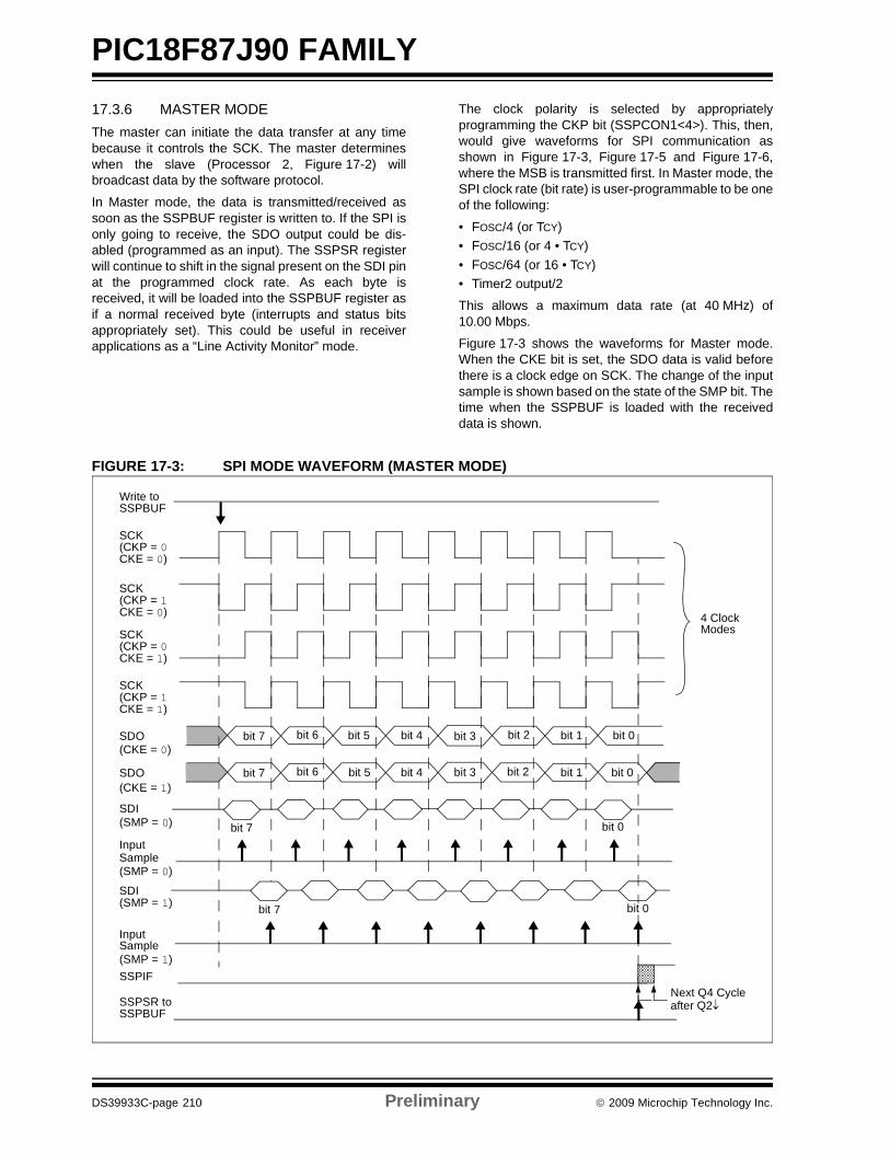
PIC18F87J90 FAMILY
DS39933C-page 210 Preliminary © 2009 Microchip Technology Inc.
17.3.6 MASTER MODEThe master can initiate the data transfer at any timebecause it controls the SCK. The master determineswhen the slave (Processor 2, Figure 17-2) willbroadcast data by the software protocol.
In Master mode, the data is transmitted/received assoon as the SSPBUF register is written to. If the SPI isonly going to receive, the SDO output could be dis-abled (programmed as an input). The SSPSR registerwill continue to shift in the signal present on the SDI pinat the programmed clock rate. As each byte isreceived, it will be loaded into the SSPBUF register asif a normal received byte (interrupts and status bitsappropriately set). This could be useful in receiverapplications as a “Line Activity Monitor” mode.
The clock polarity is selected by appropriatelyprogramming the CKP bit (SSPCON1<4>). This, then,would give waveforms for SPI communication asshown in Figure 17-3, Figure 17-5 and Figure 17-6,where the MSB is transmitted first. In Master mode, theSPI clock rate (bit rate) is user-programmable to be oneof the following:
• FOSC/4 (or TCY)• FOSC/16 (or 4 • TCY)• FOSC/64 (or 16 • TCY)• Timer2 output/2
This allows a maximum data rate (at 40 MHz) of10.00 Mbps.
Figure 17-3 shows the waveforms for Master mode.When the CKE bit is set, the SDO data is valid beforethere is a clock edge on SCK. The change of the inputsample is shown based on the state of the SMP bit. Thetime when the SSPBUF is loaded with the receiveddata is shown.
FIGURE 17-3: SPI MODE WAVEFORM (MASTER MODE)
SCK(CKP = 0
SCK(CKP = 1
SCK(CKP = 0
SCK(CKP = 1
4 ClockModes
InputSample
InputSample
SDI
bit 7 bit 0
SDO bit 7 bit 6 bit 5 bit 4 bit 3 bit 2 bit 1 bit 0
bit 7SDI
SSPIF(SMP = 1)
(SMP = 0)
(SMP = 1)
CKE = 1)
CKE = 0)
CKE = 1)
CKE = 0)
(SMP = 0)
Write toSSPBUF
SSPSR toSSPBUF
SDO bit 7 bit 6 bit 5 bit 4 bit 3 bit 2 bit 1 bit 0
(CKE = 0)
(CKE = 1)
Next Q4 Cycleafter Q2↓
bit 0
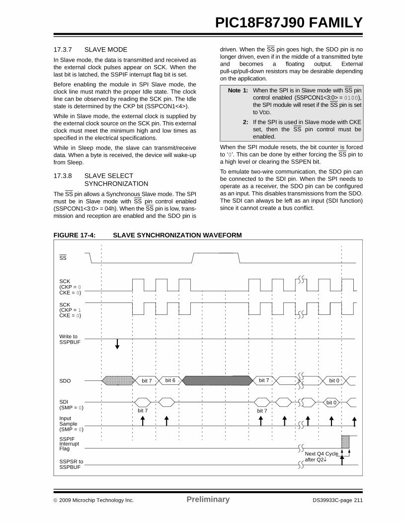
© 2009 Microchip Technology Inc. Preliminary DS39933C-page 211
PIC18F87J90 FAMILY17.3.7 SLAVE MODEIn Slave mode, the data is transmitted and received asthe external clock pulses appear on SCK. When thelast bit is latched, the SSPIF interrupt flag bit is set.
Before enabling the module in SPI Slave mode, theclock line must match the proper Idle state. The clockline can be observed by reading the SCK pin. The Idlestate is determined by the CKP bit (SSPCON1<4>).
While in Slave mode, the external clock is supplied bythe external clock source on the SCK pin. This externalclock must meet the minimum high and low times asspecified in the electrical specifications.
While in Sleep mode, the slave can transmit/receivedata. When a byte is received, the device will wake-upfrom Sleep.
17.3.8 SLAVE SELECT SYNCHRONIZATION
The SS pin allows a Synchronous Slave mode. The SPImust be in Slave mode with SS pin control enabled(SSPCON1<3:0> = 04h). When the SS pin is low, trans-mission and reception are enabled and the SDO pin is
driven. When the SS pin goes high, the SDO pin is nolonger driven, even if in the middle of a transmitted byteand becomes a floating output. Externalpull-up/pull-down resistors may be desirable dependingon the application.
When the SPI module resets, the bit counter is forcedto ‘0’. This can be done by either forcing the SS pin toa high level or clearing the SSPEN bit.
To emulate two-wire communication, the SDO pin canbe connected to the SDI pin. When the SPI needs tooperate as a receiver, the SDO pin can be configuredas an input. This disables transmissions from the SDO.The SDI can always be left as an input (SDI function)since it cannot create a bus conflict.
FIGURE 17-4: SLAVE SYNCHRONIZATION WAVEFORM
Note 1: When the SPI is in Slave mode with SS pincontrol enabled (SSPCON1<3:0> = 0100),the SPI module will reset if the SS pin is setto VDD.
2: If the SPI is used in Slave mode with CKEset, then the SS pin control must beenabled.
SCK(CKP = 1
SCK(CKP = 0
InputSample
SDI
bit 7
SDO bit 7 bit 6 bit 7
SSPIFInterrupt
(SMP = 0)
CKE = 0)
CKE = 0)
(SMP = 0)
Write toSSPBUF
SSPSR toSSPBUF
SS
Flag
bit 0
bit 7bit 0
Next Q4 Cycleafter Q2↓
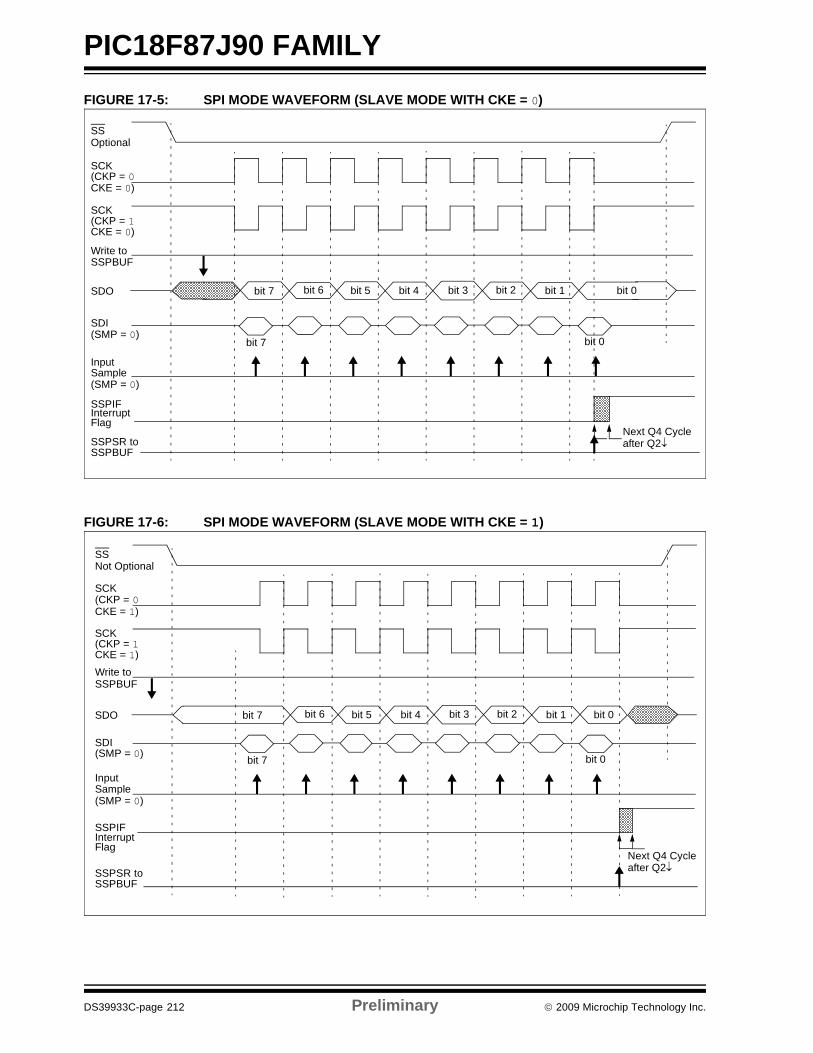
PIC18F87J90 FAMILY
DS39933C-page 212 Preliminary © 2009 Microchip Technology Inc.
FIGURE 17-5: SPI MODE WAVEFORM (SLAVE MODE WITH CKE = 0)
FIGURE 17-6: SPI MODE WAVEFORM (SLAVE MODE WITH CKE = 1)
SCK(CKP = 1
SCK(CKP = 0
InputSample
SDI
bit 7
SDO bit 7 bit 6 bit 5 bit 4 bit 3 bit 2 bit 1 bit 0
SSPIFInterrupt
(SMP = 0)
CKE = 0)
CKE = 0)
(SMP = 0)
Write toSSPBUF
SSPSR toSSPBUF
SS
Flag
Optional
Next Q4 Cycleafter Q2↓
bit 0
SCK(CKP = 1
SCK(CKP = 0
InputSample
SDI
bit 7 bit 0
SDO bit 7 bit 6 bit 5 bit 4 bit 3 bit 2 bit 1 bit 0
SSPIFInterrupt
(SMP = 0)
CKE = 1)
CKE = 1)
(SMP = 0)
Write toSSPBUF
SSPSR toSSPBUF
SS
Flag
Not Optional
Next Q4 Cycleafter Q2↓
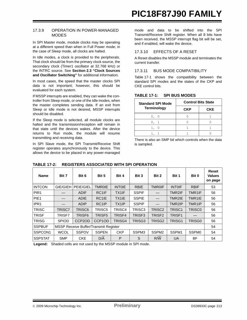
© 2009 Microchip Technology Inc. Preliminary DS39933C-page 213
PIC18F87J90 FAMILY17.3.9 OPERATION IN POWER-MANAGED
MODES
In SPI Master mode, module clocks may be operatingat a different speed than when in Full Power mode; inthe case of Sleep mode, all clocks are halted.
In Idle modes, a clock is provided to the peripherals.That clock should be from the primary clock source, thesecondary clock (Timer1 oscillator at 32.768 kHz) orthe INTRC source. See Section 2.3 “Clock Sourcesand Oscillator Switching” for additional information.
In most cases, the speed that the master clocks SPIdata is not important; however, this should beevaluated for each system.
If MSSP interrupts are enabled, they can wake the con-troller from Sleep mode, or one of the Idle modes, whenthe master completes sending data. If an exit fromSleep or Idle mode is not desired, MSSP interruptsshould be disabled.
If the Sleep mode is selected, all module clocks arehalted and the transmission/reception will remain inthat state until the devices wakes. After the devicereturns to Run mode, the module will resumetransmitting and receiving data.
In SPI Slave mode, the SPI Transmit/Receive Shiftregister operates asynchronously to the device. Thisallows the device to be placed in any power-managed
mode and data to be shifted into the SPITransmit/Receive Shift register. When all 8 bits havebeen received, the MSSP interrupt flag bit will be set,and if enabled, will wake the device.
17.3.10 EFFECTS OF A RESETA Reset disables the MSSP module and terminates thecurrent transfer.
17.3.11 BUS MODE COMPATIBILITYTable 17-1 shows the compatibility between thestandard SPI modes and the states of the CKP andCKE control bits.
TABLE 17-1: SPI BUS MODES
There is also an SMP bit which controls when the datais sampled.
TABLE 17-2: REGISTERS ASSOCIATED WITH SPI OPERATION
Standard SPI Mode Terminology
Control Bits State
CKP CKE
0, 0 0 1
0, 1 0 0
1, 0 1 1
1, 1 1 0
Name Bit 7 Bit 6 Bit 5 Bit 4 Bit 3 Bit 2 Bit 1 Bit 0Reset Values
on page
INTCON GIE/GIEH PEIE/GIEL TMR0IE INT0IE RBIE TMR0IF INT0IF RBIF 53PIR1 — ADIF RC1IF TX1IF SSPIF — TMR2IF TMR1IF 56PIE1 — ADIE RC1IE TX1IE SSPIE — TMR2IE TMR1IE 56IPR1 — ADIP RC1IP TX1IP SSPIP — TMR2IP TMR1IP 56TRISC TRISC7 TRISC6 TRISC5 TRISC4 TRISC3 TRISC2 TRISC1 TRISC0 56TRISF TRISF7 TRISF6 TRISF5 TRISF4 TRISF3 TRISF2 TRISF1 — 56TRISG SPIOD CCP2OD CCP1OD TRISG4 TRISG3 TRISG2 TRISG1 TRISG0 56SSPBUF MSSP Receive Buffer/Transmit Register 54SSPCON1 WCOL SSPOV SSPEN CKP SSPM3 SSPM2 SSPM1 SSPM0 54
SSPSTAT SMP CKE D/A P S R/W UA BF 54Legend: Shaded cells are not used by the MSSP module in SPI mode.
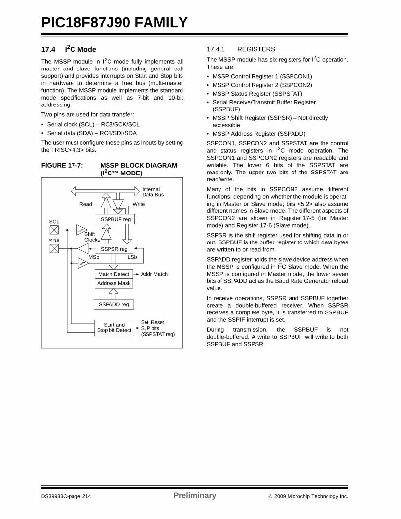
PIC18F87J90 FAMILY
DS39933C-page 214 Preliminary © 2009 Microchip Technology Inc.
17.4 I2C ModeThe MSSP module in I2C mode fully implements allmaster and slave functions (including general callsupport) and provides interrupts on Start and Stop bitsin hardware to determine a free bus (multi-masterfunction). The MSSP module implements the standardmode specifications as well as 7-bit and 10-bitaddressing.
Two pins are used for data transfer:
• Serial clock (SCL) – RC3/SCK/SCL• Serial data (SDA) – RC4/SDI/SDA
The user must configure these pins as inputs by settingthe TRISC<4:3> bits.
FIGURE 17-7: MSSP BLOCK DIAGRAM (I2C™ MODE)
17.4.1 REGISTERSThe MSSP module has six registers for I2C operation.These are:
• MSSP Control Register 1 (SSPCON1)• MSSP Control Register 2 (SSPCON2)• MSSP Status Register (SSPSTAT)• Serial Receive/Transmit Buffer Register
(SSPBUF)• MSSP Shift Register (SSPSR) – Not directly
accessible• MSSP Address Register (SSPADD)
SSPCON1, SSPCON2 and SSPSTAT are the controland status registers in I2C mode operation. TheSSPCON1 and SSPCON2 registers are readable andwritable. The lower 6 bits of the SSPSTAT areread-only. The upper two bits of the SSPSTAT areread/write.
Many of the bits in SSPCON2 assume differentfunctions, depending on whether the module is operat-ing in Master or Slave mode; bits <5:2> also assumedifferent names in Slave mode. The different aspects ofSSPCON2 are shown in Register 17-5 (for Mastermode) and Register 17-6 (Slave mode).
SSPSR is the shift register used for shifting data in orout. SSPBUF is the buffer register to which data bytesare written to or read from.
SSPADD register holds the slave device address whenthe MSSP is configured in I2C Slave mode. When theMSSP is configured in Master mode, the lower sevenbits of SSPADD act as the Baud Rate Generator reloadvalue.
In receive operations, SSPSR and SSPBUF togethercreate a double-buffered receiver. When SSPSRreceives a complete byte, it is transferred to SSPBUFand the SSPIF interrupt is set.
During transmission, the SSPBUF is notdouble-buffered. A write to SSPBUF will write to bothSSPBUF and SSPSR.
Read Write
SSPSR reg
Match Detect
SSPADD reg
Start andStop bit Detect
SSPBUF reg
InternalData Bus
Addr Match
Set, ResetS, P bits(SSPSTAT reg)
ShiftClock
MSb LSb
SCL
SDA
Address Mask
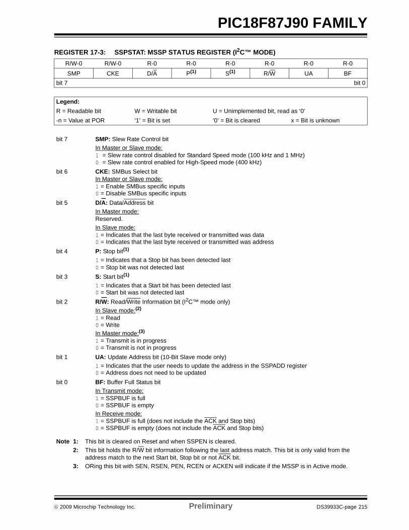
© 2009 Microchip Technology Inc. Preliminary DS39933C-page 215
PIC18F87J90 FAMILY
REGISTER 17-3: SSPSTAT: MSSP STATUS REGISTER (I2C™ MODE) R/W-0 R/W-0 R-0 R-0 R-0 R-0 R-0 R-0
SMP CKE D/A P(1) S(1) R/W UA BFbit 7 bit 0
Legend:R = Readable bit W = Writable bit U = Unimplemented bit, read as ‘0’-n = Value at POR ‘1’ = Bit is set ‘0’ = Bit is cleared x = Bit is unknown
bit 7 SMP: Slew Rate Control bitIn Master or Slave mode: 1 = Slew rate control disabled for Standard Speed mode (100 kHz and 1 MHz) 0 = Slew rate control enabled for High-Speed mode (400 kHz)
bit 6 CKE: SMBus Select bitIn Master or Slave mode:1 = Enable SMBus specific inputs 0 = Disable SMBus specific inputs
bit 5 D/A: Data/Address bit In Master mode:Reserved.In Slave mode:1 = Indicates that the last byte received or transmitted was data0 = Indicates that the last byte received or transmitted was address
bit 4 P: Stop bit(1)
1 = Indicates that a Stop bit has been detected last0 = Stop bit was not detected last
bit 3 S: Start bit(1)
1 = Indicates that a Start bit has been detected last0 = Start bit was not detected last
bit 2 R/W: Read/Write Information bit (I2C™ mode only)In Slave mode:(2)
1 = Read0 = WriteIn Master mode:(3)
1 = Transmit is in progress0 = Transmit is not in progress
bit 1 UA: Update Address bit (10-Bit Slave mode only)1 = Indicates that the user needs to update the address in the SSPADD register 0 = Address does not need to be updated
bit 0 BF: Buffer Full Status bitIn Transmit mode: 1 = SSPBUF is full 0 = SSPBUF is emptyIn Receive mode:1 = SSPBUF is full (does not include the ACK and Stop bits)0 = SSPBUF is empty (does not include the ACK and Stop bits)
Note 1: This bit is cleared on Reset and when SSPEN is cleared.2: This bit holds the R/W bit information following the last address match. This bit is only valid from the
address match to the next Start bit, Stop bit or not ACK bit.3: ORing this bit with SEN, RSEN, PEN, RCEN or ACKEN will indicate if the MSSP is in Active mode.
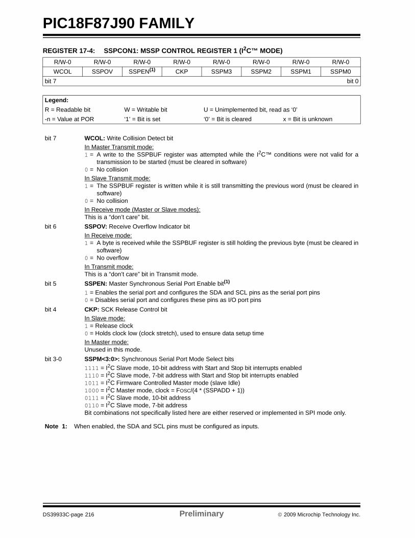
PIC18F87J90 FAMILY
DS39933C-page 216 Preliminary © 2009 Microchip Technology Inc.
REGISTER 17-4: SSPCON1: MSSP CONTROL REGISTER 1 (I2C™ MODE) R/W-0 R/W-0 R/W-0 R/W-0 R/W-0 R/W-0 R/W-0 R/W-0WCOL SSPOV SSPEN(1) CKP SSPM3 SSPM2 SSPM1 SSPM0
bit 7 bit 0
Legend:R = Readable bit W = Writable bit U = Unimplemented bit, read as ‘0’-n = Value at POR ‘1’ = Bit is set ‘0’ = Bit is cleared x = Bit is unknown
bit 7 WCOL: Write Collision Detect bitIn Master Transmit mode:1 = A write to the SSPBUF register was attempted while the I2C™ conditions were not valid for a
transmission to be started (must be cleared in software)0 = No collisionIn Slave Transmit mode:1 = The SSPBUF register is written while it is still transmitting the previous word (must be cleared in
software)0 = No collision In Receive mode (Master or Slave modes):This is a “don’t care” bit.
bit 6 SSPOV: Receive Overflow Indicator bit In Receive mode:1 = A byte is received while the SSPBUF register is still holding the previous byte (must be cleared in
software)0 = No overflowIn Transmit mode: This is a “don’t care” bit in Transmit mode.
bit 5 SSPEN: Master Synchronous Serial Port Enable bit(1) 1 = Enables the serial port and configures the SDA and SCL pins as the serial port pins 0 = Disables serial port and configures these pins as I/O port pins
bit 4 CKP: SCK Release Control bit In Slave mode: 1 = Release clock 0 = Holds clock low (clock stretch), used to ensure data setup timeIn Master mode: Unused in this mode.
bit 3-0 SSPM<3:0>: Synchronous Serial Port Mode Select bits1111 = I2C Slave mode, 10-bit address with Start and Stop bit interrupts enabled1110 = I2C Slave mode, 7-bit address with Start and Stop bit interrupts enabled1011 = I2C Firmware Controlled Master mode (slave Idle)1000 = I2C Master mode, clock = FOSC/(4 * (SSPADD + 1)) 0111 = I2C Slave mode, 10-bit address0110 = I2C Slave mode, 7-bit addressBit combinations not specifically listed here are either reserved or implemented in SPI mode only.
Note 1: When enabled, the SDA and SCL pins must be configured as inputs.

© 2009 Microchip Technology Inc. Preliminary DS39933C-page 217
PIC18F87J90 FAMILY
REGISTER 17-5: SSPCON2: MSSP CONTROL REGISTER 2 (I2C™ MASTER MODE) R/W-0 R/W-0 R/W-0 R/W-0 R/W-0 R/W-0 R/W-0 R/W-0GCEN ACKSTAT ACKDT(1) ACKEN(2) RCEN(2) PEN(2) RSEN(2) SEN(2)
bit 7 bit 0
Legend:R = Readable bit W = Writable bit U = Unimplemented bit, read as ‘0’-n = Value at POR ‘1’ = Bit is set ‘0’ = Bit is cleared x = Bit is unknown
bit 7 GCEN: General Call Enable bitUnused in Master mode.
bit 6 ACKSTAT: Acknowledge Status bit (Master Transmit mode only)1 = Acknowledge was not received from slave 0 = Acknowledge was received from slave
bit 5 ACKDT: Acknowledge Data bit (Master Receive mode only)(1)
1 = Not Acknowledge 0 = Acknowledge
bit 4 ACKEN: Acknowledge Sequence Enable bit(2)
1 = Initiate Acknowledge sequence on SDA and SCL pins and transmit ACKDT data bit. Automaticallycleared by hardware.
0 = Acknowledge sequence Idlebit 3 RCEN: Receive Enable bit (Master Receive mode only)(2)
1 = Enables Receive mode for I2C™ 0 = Receive Idle
bit 2 PEN: Stop Condition Enable bit(2)
1 = Initiate Stop condition on SDA and SCL pins. Automatically cleared by hardware. 0 = Stop condition Idle
bit 1 RSEN: Repeated Start Condition Enable bit(2)
1 = Initiate Repeated Start condition on SDA and SCL pins. Automatically cleared by hardware. 0 = Repeated Start condition Idle
bit 0 SEN: Start Condition Enable bit(2)
1 = Initiate Start condition on SDA and SCL pins. Automatically cleared by hardware. 0 = Start condition Idle
Note 1: Value that will be transmitted when the user initiates an Acknowledge sequence at the end of a receive.2: If the I2C module is active, these bits may not be set (no spooling) and the SSPBUF may not be written (or
writes to the SSPBUF are disabled).
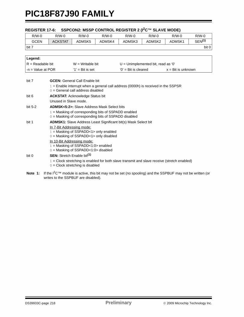
PIC18F87J90 FAMILY
DS39933C-page 218 Preliminary © 2009 Microchip Technology Inc.
REGISTER 17-6: SSPCON2: MSSP CONTROL REGISTER 2 (I2C™ SLAVE MODE) R/W-0 R/W-0 R/W-0 R/W-0 R/W-0 R/W-0 R/W-0 R/W-0GCEN ACKSTAT ADMSK5 ADMSK4 ADMSK3 ADMSK2 ADMSK1 SEN(1)
bit 7 bit 0
Legend:R = Readable bit W = Writable bit U = Unimplemented bit, read as ‘0’-n = Value at POR ‘1’ = Bit is set ‘0’ = Bit is cleared x = Bit is unknown
bit 7 GCEN: General Call Enable bit1 = Enable interrupt when a general call address (0000h) is received in the SSPSR 0 = General call address disabled
bit 6 ACKSTAT: Acknowledge Status bitUnused in Slave mode.
bit 5-2 ADMSK<5:2>: Slave Address Mask Select bits1 = Masking of corresponding bits of SSPADD enabled 0 = Masking of corresponding bits of SSPADD disabled
bit 1 ADMSK1: Slave Address Least Significant bit(s) Mask Select bitIn 7-Bit Addressing mode:1 = Masking of SSPADD<1> only enabled 0 = Masking of SSPADD<1> only disabledIn 10-Bit Addressing mode:1 = Masking of SSPADD<1:0> enabled 0 = Masking of SSPADD<1:0> disabled
bit 0 SEN: Stretch Enable bit(1)
1 = Clock stretching is enabled for both slave transmit and slave receive (stretch enabled)0 = Clock stretching is disabled
Note 1: If the I2C™ module is active, this bit may not be set (no spooling) and the SSPBUF may not be written (or writes to the SSPBUF are disabled).
© 2009 Microchip Technology Inc. Preliminary DS39933C-page 219
PIC18F87J90 FAMILY
17.4.2 OPERATIONThe MSSP module functions are enabled by setting theMSSP Enable bit, SSPEN (SSPCON1<5>).
The SSPCON1 register allows control of the I2Coperation. Four mode selection bits (SSPCON1<3:0>)allow one of the following I2C modes to be selected:
• I2C Master mode, clock = (FOSC/4) x (SSPADD + 1)
• I2C Slave mode (7-bit address)• I2C Slave mode (10-bit address)• I2C Slave mode (7-bit address) with Start and
Stop bit interrupts enabled• I2C Slave mode (10-bit address) with Start and
Stop bit interrupts enabled• I2C Firmware Controlled Master mode,
slave is Idle
Selection of any I2C mode, with the SSPEN bit set,forces the SCL and SDA pins to be open-drain,provided these pins are programmed to inputs bysetting the appropriate TRISC or TRISD bits. To ensureproper operation of the module, pull-up resistors mustbe provided externally to the SCL and SDA pins.
17.4.3 SLAVE MODEIn Slave mode, the SCL and SDA pins must beconfigured as inputs (TRISC<4:3> set). The MSSPmodule will override the input state with the output datawhen required (slave-transmitter).
The I2C Slave mode hardware will always generate aninterrupt on an exact address match. In addition,address masking will also allow the hardware to gener-ate an interrupt for more than one address (up to 31 in7-bit addressing and up to 63 in 10-bit addressing).Through the mode select bits, the user can also chooseto interrupt on Start and Stop bits.
When an address is matched, or the data transfer afteran address match is received, the hardware auto-matically will generate the Acknowledge (ACK) pulseand load the SSPBUF register with the received valuecurrently in the SSPSR register.
Any combination of the following conditions will causethe MSSP module not to give this ACK pulse:
• The Buffer Full bit, BF (SSPSTAT<0>), was set before the transfer was received.
• The overflow bit, SSPOV (SSPCON1<6>), was set before the transfer was received.
In this case, the SSPSR register value is not loadedinto the SSPBUF, but bit SSPIF is set. The BF bit iscleared by reading the SSPBUF register, while bitSSPOV is cleared through software.
The SCL clock input must have a minimum high andlow for proper operation. The high and low times of theI2C specification, as well as the requirement of theMSSP module, are shown in timing parameter 100 andparameter 101.
17.4.3.1 AddressingOnce the MSSP module has been enabled, it waits for aStart condition to occur. Following the Start condition, the8 bits are shifted into the SSPSR register. All incomingbits are sampled with the rising edge of the clock (SCL)line. The value of register SSPSR<7:1> is compared tothe value of the SSPADD register. The address is com-pared on the falling edge of the eighth clock (SCL) pulse.If the addresses match and the BF and SSPOV bits areclear, the following events occur:
1. The SSPSR register value is loaded into theSSPBUF register.
2. The Buffer Full bit, BF, is set.3. An ACK pulse is generated.4. The MSSP Interrupt Flag bit, SSPIF, is set (and
interrupt is generated, if enabled) on the fallingedge of the ninth SCL pulse.
In 10-Bit Addressing mode, two address bytes need tobe received by the slave. The five Most Significant bits(MSbs) of the first address byte specify if this is a 10-bitaddress. Bit R/W (SSPSTAT<2>) must specify a writeso the slave device will receive the second addressbyte. For a 10-bit address, the first byte would equal‘11110 A9 A8 0’, where ‘A9’ and ‘A8’ are the twoMSbs of the address. The sequence of events for 10-bitaddressing is as follows, with steps 7 through 9 for theslave-transmitter:
1. Receive first (high) byte of address (bits SSPIF,BF and UA (SSPSTAT<1>) are set).
2. Update the SSPADD register with second (low)byte of address (clears bit UA and releases theSCL line).
3. Read the SSPBUF register (clears bit BF) andclear flag bit, SSPIF.
4. Receive second (low) byte of address (SSPIF,BF and UA bits are set).
5. Update the SSPADD register with the first (high)byte of address. If match releases SCL line, thiswill clear UA bit.
6. Read the SSPBUF register (clears bit BF) andclear flag bit, SSPIF.
7. Receive Repeated Start condition.8. Receive first (high) byte of address (SSPIF and
BF bits are set).9. Read the SSPBUF register (clears BF bit) and
clear flag bit, SSPIF.
PIC18F87J90 FAMILY
DS39933C-page 220 Preliminary © 2009 Microchip Technology Inc.
17.4.3.2 Address MaskingMasking an address bit causes that bit to become a“don’t care”. When one address bit is masked, twoaddresses will be Acknowledged and cause aninterrupt. It is possible to mask more than one addressbit at a time, which makes it possible to Acknowledgeup to 31 addresses in 7-bit mode and up to63 addresses in 10-bit mode (see Example 17-2).
The I2C Slave behaves the same way whether addressmasking is used or not. However, when addressmasking is used, the I2C slave can Acknowledgemultiple addresses and cause interrupts. When thisoccurs, it is necessary to determine which addresscaused the interrupt by checking SSPBUF.
In 7-Bit Addressing mode, address mask bits,ADMSK<5:1> (SSPCON<5:1>), mask the correspond-ing address bits in the SSPADD register. For any ADMSKbits that are set (ADMSK<n> = 1), the correspondingaddress bit is ignored (SSPADD<n> = x). For the moduleto issue an address Acknowledge, it is sufficient to matchonly on addresses that do not have an active addressmask.
In 10-Bit Addressing mode, ADMSK<5:2> bits maskthe corresponding address bits in the SSPADD regis-ter. In addition, ADMSK1 simultaneously masks the twoLSbs of the address (SSPADD<1:0>). For any ADMSKbits that are active (ADMSK<n> = 1), the correspond-ing address bit is ignored (SSPADD<n> = x). Also notethat although in 10-Bit Addressing mode, the upperaddress bits reuse part of the SSPADD register bits, theaddress mask bits do not interact with those bits. Theyonly affect the lower address bits.
EXAMPLE 17-2: ADDRESS MASKING EXAMPLES
Note 1: ADMSK1 masks the two Least Significantbits of the address.
2: The two Most Significant bits of theaddress are not affected by addressmasking.
7-Bit Addressing:SSPADD<7:1> = A0h (1010000) (SSPADD<0> is assumed to be ‘0’)
ADMSK<5:1> = 00111
Addresses Acknowledged: A0h, A2h, A4h, A6h, A8h, AAh, ACh, AEh
10-Bit Addressing:SSPADD<7:0> = A0h (10100000) (the two MSbs of the address are ignored in this example, since they arenot affected by masking)
ADMSK<5:1> = 00111
Addresses Acknowledged: A0h, A1h, A2h, A3h, A4h, A5h, A6h, A7h, A8h, A9h, AAh, ABh, ACh, ADh, AEh, AFh
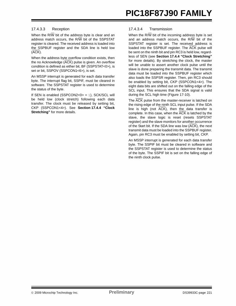
© 2009 Microchip Technology Inc. Preliminary DS39933C-page 221
PIC18F87J90 FAMILY17.4.3.3 ReceptionWhen the R/W bit of the address byte is clear and anaddress match occurs, the R/W bit of the SSPSTATregister is cleared. The received address is loaded intothe SSPBUF register and the SDA line is held low(ACK).
When the address byte overflow condition exists, thenthe no Acknowledge (ACK) pulse is given. An overflowcondition is defined as either bit, BF (SSPSTAT<0>), isset or bit, SSPOV (SSPCON1<6>), is set.
An MSSP interrupt is generated for each data transferbyte. The interrupt flag bit, SSPIF, must be cleared insoftware. The SSPSTAT register is used to determinethe status of the byte.
If SEN is enabled (SSPCON2<0> = 1), SCK/SCL willbe held low (clock stretch) following each datatransfer. The clock must be released by setting bit,CKP (SSPCON1<4>). See Section 17.4.4 “ClockStretching” for more details.
17.4.3.4 TransmissionWhen the R/W bit of the incoming address byte is setand an address match occurs, the R/W bit of theSSPSTAT register is set. The received address isloaded into the SSPBUF register. The ACK pulse willbe sent on the ninth bit and pin RC3 is held low, regard-less of SEN (see Section 17.4.4 “Clock Stretching”for more details). By stretching the clock, the masterwill be unable to assert another clock pulse until theslave is done preparing the transmit data. The transmitdata must be loaded into the SSPBUF register whichalso loads the SSPSR register. Then, pin RC3 shouldbe enabled by setting bit, CKP (SSPCON1<4>). Theeight data bits are shifted out on the falling edge of theSCL input. This ensures that the SDA signal is validduring the SCL high time (Figure 17-10).
The ACK pulse from the master-receiver is latched onthe rising edge of the ninth SCL input pulse. If the SDAline is high (not ACK), then the data transfer iscomplete. In this case, when the ACK is latched by theslave, the slave logic is reset (resets SSPSTATregister) and the slave monitors for another occurrenceof the Start bit. If the SDA line was low (ACK), the nexttransmit data must be loaded into the SSPBUF register.Again, pin RC3 must be enabled by setting bit, CKP.
An MSSP interrupt is generated for each data transferbyte. The SSPIF bit must be cleared in software andthe SSPSTAT register is used to determine the statusof the byte. The SSPIF bit is set on the falling edge ofthe ninth clock pulse.
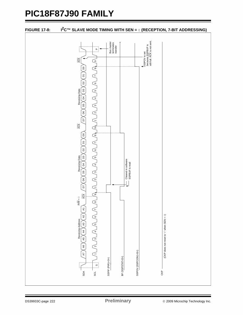
PIC18F87J90 FAMILY
DS39933C-page 222 Preliminary © 2009 Microchip Technology Inc.
FIGURE 17-8: I2C™ SLAVE MODE TIMING WITH SEN = 0 (RECEPTION, 7-BIT ADDRESSING)
SD
A
SC
L
SSP
IF (P
IR1<
3>)
BF
(SSP
STAT
<0>)
SSPO
V (S
SPC
ON
1<6>
)
S1
23
45
67
89
12
34
56
78
91
23
45
78
9P
A7A
6A5
A4A3
A2A
1D
7D
6D
5D
4D
3D
2D
1D
0D
7D
6D
5D
4D
3D
1D
0
ACK
Rec
eivi
ng D
ata
AC
KR
ecei
ving
Dat
aR
/W =
0 AC
K
Rec
eivi
ng A
ddre
ss
Cle
ared
in s
oftw
are
SSP
BU
F is
read
Bus
mas
ter
term
inat
estra
nsfe
r
SSP
OV
is s
etbe
caus
e S
SPB
UF
isst
ill fu
ll. A
CK
is n
ot s
ent.
D2 6
CK
P(C
KP
does
not
rese
t to
‘0’ w
hen
SEN
= 0
)
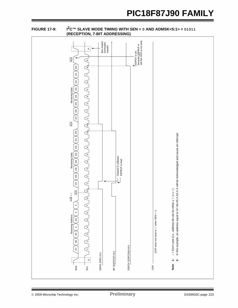
© 2009 Microchip Technology Inc. Preliminary DS39933C-page 223
PIC18F87J90 FAMILYFIGURE 17-9: I2C™ SLAVE MODE TIMING WITH SEN = 0 AND ADMSK<5:1> = 01011
(RECEPTION, 7-BIT ADDRESSING)
SDA
SCL
SSP
IF (P
IR1<
3>)
BF (S
SPS
TAT<
0>)
SSP
OV
(SSP
CO
N1<
6>)
S1
23
45
67
89
12
34
56
78
91
23
45
78
9P
A7A6
A5
XA3
XX
D7
D6
D5
D4
D3
D2
D1
D0
D7
D6
D5
D4
D3
D1
D0
ACK
Rec
eivi
ng D
ata
ACK
Rec
eivi
ng D
ata
R/W
= 0 AC
K
Rec
eivi
ng A
ddre
ss
Cle
ared
in s
oftw
are
SSPB
UF
is re
ad
Bus
mas
ter
term
inat
estra
nsfe
r
SSPO
V is
set
beca
use
SSP
BUF
isst
ill fu
ll. A
CK
is n
ot s
ent.
D2 6
CKP
(CKP
doe
s no
t res
et to
‘0’ w
hen
SEN
= 0
)
Not
e1:
x =
Don
’t ca
re (i
.e.,
addr
ess
bit c
an b
e ei
ther
a ‘1
’ or a
‘0’).
2:In
this
exa
mpl
e, a
n ad
dres
s eq
ual t
o A
7.A
6.A
5.X
.A3.
X.X
will
be
Ack
now
ledg
ed a
nd c
ause
an
inte
rrupt
.
PIC18F87J90 FAMILY
DS39933C-page 224 Preliminary © 2009 Microchip Technology Inc.
FIGURE 17-10: I2C™ SLAVE MODE TIMING (TRANSMISSION, 7-BIT ADDRESSING)
SDAx
SCLx
BF (S
SPxS
TAT<
0>)
A6A5
A4A3
A2A1
D6
D5
D4
D3
D2
D1
D0
12
34
56
78
23
45
67
89
SSPx
BUF
is w
ritte
n in
sof
twar
e
Cle
ared
in s
oftw
are
Dat
a in
sa
mpl
ed
S
ACK
Tran
smitt
ing
Dat
aR
/W =
1
ACK
Rec
eivi
ng A
ddre
ss
A7D
7
91
D6
D5
D4
D3
D2
D1
D0
23
45
67
89
SSPx
BUF
is w
ritte
n in
sof
twar
e
Cle
ared
in s
oftw
are
From
SSP
xIF
ISR
Tran
smitt
ing
Dat
a
D7 1
CKP
(SSP
xCO
N1<
4>)
P
ACK
CKP
is s
et in
sof
twar
eC
KP is
set
in s
oftw
are
SCLx
hel
d lo
ww
hile
CPU
resp
onds
to S
SPxI
F
SSPx
IF (P
IR1<
3> o
r PIR
3<7>
)
From
SSP
xIF
ISR
Cle
ar b
y re
adin
g
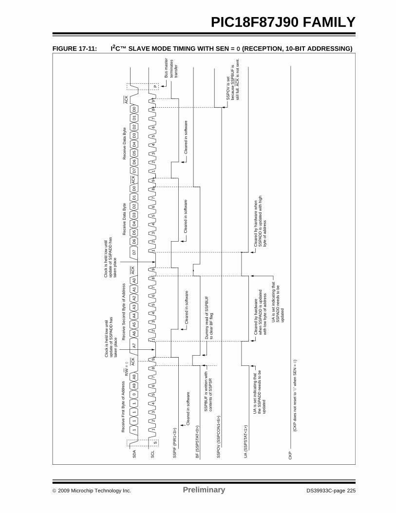
© 2009 Microchip Technology Inc. Preliminary DS39933C-page 225
PIC18F87J90 FAMILYFIGURE 17-11: I2C™ SLAVE MODE TIMING WITH SEN = 0 (RECEPTION, 10-BIT ADDRESSING)
SDA
SCL
SSPI
F (P
IR1<
3>)
BF (S
SPS
TAT<
0>)
S1
23
45
67
89
12
34
56
78
91
23
45
78
9P
11
11
0A
9A
8A7
A6A5
A4A
3A2
A1A0
D7
D6
D5
D4
D3
D1
D0
Rec
eive
Dat
a B
yte
ACK
R/W
= 0 AC
K
Rec
eive
Firs
t Byt
e of
Add
ress
Cle
ared
in s
oftw
are
D2 6
Cle
ared
in s
oftw
are
Rec
eive
Sec
ond
Byte
of A
ddre
ss
Cle
ared
by
hard
war
ew
hen
SSPA
DD
is u
pdat
edw
ith lo
w b
yte
of a
ddre
ss
UA
(SS
PSTA
T<1>
)
Clo
ck is
hel
d lo
w u
ntil
upda
te o
f SS
PAD
D h
as
take
n pl
ace
UA
is s
et in
dica
ting
that
the
SSPA
DD
nee
ds to
be
upda
ted
UA
is s
et in
dica
ting
that
SSPA
DD
nee
ds to
be
upda
ted
Cle
ared
by
hard
war
e w
hen
SSPA
DD
is u
pdat
ed w
ith h
igh
byte
of a
ddre
ss
SSP
BUF
is w
ritte
n w
ithco
nten
ts o
f SSP
SR
Dum
my
read
of S
SPB
UF
to c
lear
BF
flag
AC
K
CK
P
12
34
57
89
D7
D6
D5
D4
D3
D1
D0
Rec
eive
Dat
a B
yte
Bus
mas
ter
term
inat
estra
nsfe
r
D2 6
AC
K
Cle
ared
in s
oftw
are
Cle
ared
in s
oftw
are
SSPO
V (S
SPC
ON
1<6>
)
SSP
OV
is s
etbe
caus
e S
SPB
UF
isst
ill fu
ll. A
CK
is n
ot s
ent.
(CKP
doe
s no
t res
et to
‘0’ w
hen
SEN
= 0
)
Clo
ck is
hel
d lo
w u
ntil
upda
te o
f SSP
ADD
has
ta
ken
plac
e
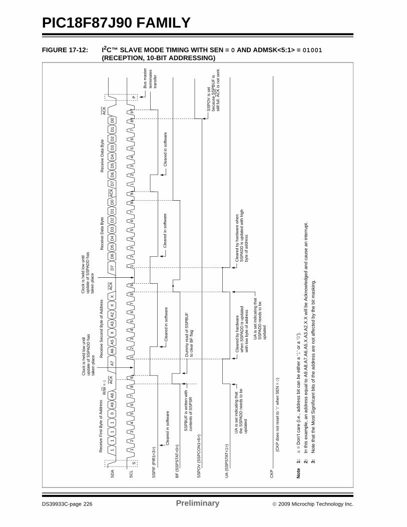
PIC18F87J90 FAMILY
DS39933C-page 226 Preliminary © 2009 Microchip Technology Inc.
FIGURE 17-12: I2C™ SLAVE MODE TIMING WITH SEN = 0 AND ADMSK<5:1> = 01001 (RECEPTION, 10-BIT ADDRESSING)
SD
A
SC
L
SSP
IF (P
IR1<
3>)
BF
(SSP
STAT
<0>)
S1
23
45
67
89
12
34
56
78
91
23
45
78
9P
11
11
0A9
A8A7
A6A
5X
A3A
2X
XD
7D
6D
5D
4D
3D
1D
0
Rec
eive
Dat
a B
yte
ACK
R/W
= 0 AC
K
Rec
eive
Firs
t Byt
e of
Add
ress
Cle
ared
in s
oftw
are
D2 6
Cle
ared
in s
oftw
are
Rec
eive
Sec
ond
Byte
of A
ddre
ss
Cle
ared
by
hard
war
ew
hen
SSPA
DD
is u
pdat
edw
ith lo
w b
yte
of a
ddre
ss
UA
(SSP
STA
T<1>
)
Clo
ck is
hel
d lo
w u
ntil
upda
te o
f SSP
ADD
has
ta
ken
plac
e
UA
is s
et in
dica
ting
that
the
SSPA
DD
nee
ds to
be
upda
ted
UA
is s
et in
dica
ting
that
SSPA
DD
nee
ds to
be
upda
ted
Cle
ared
by
hard
war
e w
hen
SSPA
DD
is u
pdat
ed w
ith h
igh
byte
of a
ddre
ss
SS
PB
UF
is w
ritte
n w
ithco
nten
ts o
f SS
PSR
Dum
my
read
of S
SPB
UF
to c
lear
BF
flag
AC
K
CK
P
12
34
57
89
D7
D6
D5
D4
D3
D1
D0
Rec
eive
Dat
a B
yte
Bus
mas
ter
term
inat
estra
nsfe
r
D2 6
ACK
Cle
ared
in s
oftw
are
Cle
ared
in s
oftw
are
SSP
OV
(SS
PCO
N1<
6>)
SSP
OV
is s
etbe
caus
e S
SPB
UF
isst
ill fu
ll. A
CK
is n
ot s
ent.
(CK
P do
es n
ot re
set t
o ‘0
’ whe
n S
EN =
0)
Clo
ck is
hel
d lo
w u
ntil
upda
te o
f SSP
ADD
has
ta
ken
plac
e
Not
e1:
x =
Don
’t ca
re (i
.e.,
addr
ess
bit c
an b
e ei
ther
a ‘1
’ or a
‘0’).
2:In
this
exa
mpl
e, a
n ad
dres
s eq
ual t
o A
9.A
8.A
7.A
6.A5
.X.A
3.A
2.X
.X w
ill b
e A
ckno
wle
dged
and
cau
se a
n in
terru
pt.
3:N
ote
that
the
Mos
t Sig
nific
ant b
its o
f the
add
ress
are
not
affe
cted
by
the
bit m
aski
ng.
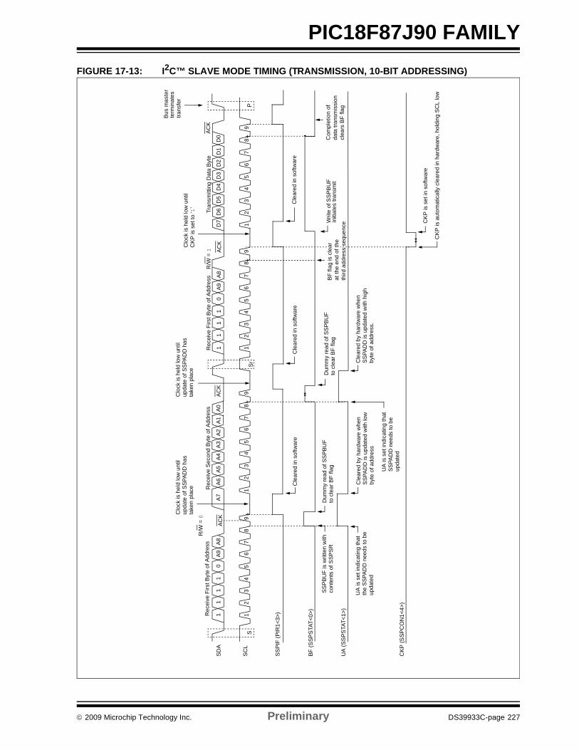
© 2009 Microchip Technology Inc. Preliminary DS39933C-page 227
PIC18F87J90 FAMILYFIGURE 17-13: I2C™ SLAVE MODE TIMING (TRANSMISSION, 10-BIT ADDRESSING)
SDA
SCL
SSPI
F (P
IR1<
3>)
BF (S
SPS
TAT<
0>)
S1
23
45
67
89
12
34
56
78
91
23
45
78
9P
11
11
0A9
A8A
7A
6A5
A4A
3A2
A1A0
11
11
0A8
R/W
= 1 AC
KA
CK
R/W
= 0
ACK
Rec
eive
Firs
t Byt
e of
Add
ress
Cle
ared
in s
oftw
are
Bus
mas
ter
term
inat
estra
nsfe
r
A9 6
Rec
eive
Sec
ond
Byte
of A
ddre
ss
Cle
ared
by
hard
war
e w
hen
SSP
ADD
is u
pdat
ed w
ith lo
wby
te o
f add
ress
UA
(SS
PSTA
T<1>
)
Clo
ck is
hel
d lo
w u
ntil
upda
te o
f SSP
ADD
has
ta
ken
plac
e
UA
is s
et in
dica
ting
that
the
SSP
ADD
nee
ds to
be
upda
ted
UA
is s
et in
dica
ting
that
SSPA
DD
nee
ds to
be
upda
ted
Cle
ared
by
hard
war
e w
hen
SSP
ADD
is u
pdat
ed w
ith h
igh
byte
of a
ddre
ss.
SSP
BUF
is w
ritte
n w
ithco
nten
ts o
f SSP
SR
Dum
my
read
of S
SPB
UF
to c
lear
BF
flag
Rec
eive
Firs
t Byt
e of
Add
ress
12
34
57
89
D7
D6
D5
D4
D3
D1
ACK
D2 6
Tran
smitt
ing
Dat
a By
te
D0
Dum
my
read
of S
SPB
UF
to c
lear
BF
flag
Sr
Cle
ared
in s
oftw
are
Writ
e of
SSP
BU
Fin
itiat
es tr
ansm
it
Cle
ared
in s
oftw
are
Com
plet
ion
of
clea
rs B
F fla
g
CKP
(SSP
CO
N1<
4>)
CK
P is
set
in s
oftw
are
CK
P is
aut
omat
ical
ly c
lear
ed in
har
dwar
e, h
oldi
ng S
CL
low
Clo
ck is
hel
d lo
w u
ntil
upda
te o
f SS
PAD
D h
as
take
n pl
ace
data
tran
smis
sion
Clo
ck is
hel
d lo
w u
ntil
CK
P is
set
to ‘1
’
third
add
ress
seq
uenc
e
BF
flag
is c
lear
at th
e en
d of
the
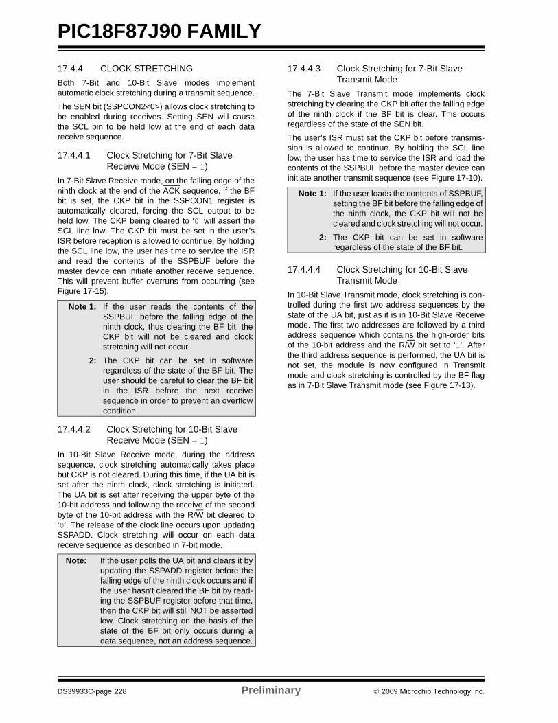
PIC18F87J90 FAMILY
DS39933C-page 228 Preliminary © 2009 Microchip Technology Inc.
17.4.4 CLOCK STRETCHINGBoth 7-Bit and 10-Bit Slave modes implementautomatic clock stretching during a transmit sequence.
The SEN bit (SSPCON2<0>) allows clock stretching tobe enabled during receives. Setting SEN will causethe SCL pin to be held low at the end of each datareceive sequence.
17.4.4.1 Clock Stretching for 7-Bit Slave Receive Mode (SEN = 1)
In 7-Bit Slave Receive mode, on the falling edge of theninth clock at the end of the ACK sequence, if the BFbit is set, the CKP bit in the SSPCON1 register isautomatically cleared, forcing the SCL output to beheld low. The CKP being cleared to ‘0’ will assert theSCL line low. The CKP bit must be set in the user’sISR before reception is allowed to continue. By holdingthe SCL line low, the user has time to service the ISRand read the contents of the SSPBUF before themaster device can initiate another receive sequence.This will prevent buffer overruns from occurring (seeFigure 17-15).
17.4.4.2 Clock Stretching for 10-Bit Slave Receive Mode (SEN = 1)
In 10-Bit Slave Receive mode, during the addresssequence, clock stretching automatically takes placebut CKP is not cleared. During this time, if the UA bit isset after the ninth clock, clock stretching is initiated.The UA bit is set after receiving the upper byte of the10-bit address and following the receive of the secondbyte of the 10-bit address with the R/W bit cleared to‘0’. The release of the clock line occurs upon updatingSSPADD. Clock stretching will occur on each datareceive sequence as described in 7-bit mode.
17.4.4.3 Clock Stretching for 7-Bit Slave Transmit Mode
The 7-Bit Slave Transmit mode implements clockstretching by clearing the CKP bit after the falling edgeof the ninth clock if the BF bit is clear. This occursregardless of the state of the SEN bit.
The user’s ISR must set the CKP bit before transmis-sion is allowed to continue. By holding the SCL linelow, the user has time to service the ISR and load thecontents of the SSPBUF before the master device caninitiate another transmit sequence (see Figure 17-10).
17.4.4.4 Clock Stretching for 10-Bit Slave Transmit Mode
In 10-Bit Slave Transmit mode, clock stretching is con-trolled during the first two address sequences by thestate of the UA bit, just as it is in 10-Bit Slave Receivemode. The first two addresses are followed by a thirdaddress sequence which contains the high-order bitsof the 10-bit address and the R/W bit set to ‘1’. Afterthe third address sequence is performed, the UA bit isnot set, the module is now configured in Transmitmode and clock stretching is controlled by the BF flagas in 7-Bit Slave Transmit mode (see Figure 17-13).
Note 1: If the user reads the contents of theSSPBUF before the falling edge of theninth clock, thus clearing the BF bit, theCKP bit will not be cleared and clockstretching will not occur.
2: The CKP bit can be set in softwareregardless of the state of the BF bit. Theuser should be careful to clear the BF bitin the ISR before the next receivesequence in order to prevent an overflowcondition.
Note: If the user polls the UA bit and clears it byupdating the SSPADD register before thefalling edge of the ninth clock occurs and ifthe user hasn’t cleared the BF bit by read-ing the SSPBUF register before that time,then the CKP bit will still NOT be assertedlow. Clock stretching on the basis of thestate of the BF bit only occurs during adata sequence, not an address sequence.
Note 1: If the user loads the contents of SSPBUF,setting the BF bit before the falling edge ofthe ninth clock, the CKP bit will not becleared and clock stretching will not occur.
2: The CKP bit can be set in softwareregardless of the state of the BF bit.
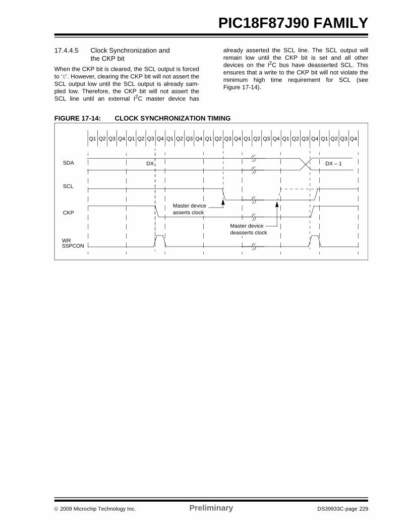
© 2009 Microchip Technology Inc. Preliminary DS39933C-page 229
PIC18F87J90 FAMILY17.4.4.5 Clock Synchronization and
the CKP bitWhen the CKP bit is cleared, the SCL output is forcedto ‘0’. However, clearing the CKP bit will not assert theSCL output low until the SCL output is already sam-pled low. Therefore, the CKP bit will not assert theSCL line until an external I2C master device has
already asserted the SCL line. The SCL output willremain low until the CKP bit is set and all otherdevices on the I2C bus have deasserted SCL. Thisensures that a write to the CKP bit will not violate theminimum high time requirement for SCL (seeFigure 17-14).
FIGURE 17-14: CLOCK SYNCHRONIZATION TIMING
SDA
SCL
DX – 1DX
WR
Q1 Q2 Q3 Q4 Q1 Q2 Q3 Q4 Q1 Q2 Q3 Q4 Q1 Q2 Q3 Q4 Q1 Q2 Q3 Q4 Q1 Q2 Q3 Q4 Q1 Q2 Q3 Q4
SSPCON
CKP
Master devicedeasserts clock
Master deviceasserts clock
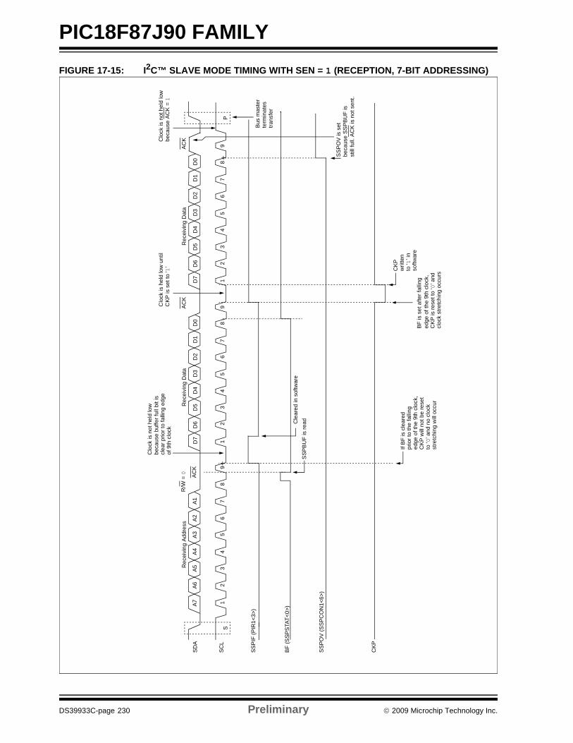
PIC18F87J90 FAMILY
DS39933C-page 230 Preliminary © 2009 Microchip Technology Inc.
FIGURE 17-15: I2C™ SLAVE MODE TIMING WITH SEN = 1 (RECEPTION, 7-BIT ADDRESSING)
SDA
SCL
SSP
IF (P
IR1<
3>)
BF (S
SPS
TAT<
0>)
SSP
OV
(SSP
CO
N1<
6>)
S1
23
45
67
89
12
34
56
78
91
23
45
78
9P
A7A6
A5A
4A
3A
2A1
D7
D6
D5
D4
D3
D2
D1
D0
D7
D6
D5
D4
D3
D1
D0
ACK
Rec
eivi
ng D
ata
AC
KR
ecei
ving
Dat
aR
/W =
0 ACK
Rec
eivi
ng A
ddre
ss
Cle
ared
in s
oftw
are
SSP
BU
F is
read
Bus
mas
ter
term
inat
estra
nsfe
r
SSP
OV
is s
etbe
caus
e SS
PBU
F is
still
full.
AC
K is
not
sen
t.
D2 6
CKP
CKP
writ
ten
to ‘1
’ in
If BF
is c
lear
edpr
ior t
o th
e fa
lling
edge
of t
he 9
th c
lock
,C
KP
will
not b
e re
set
to ‘0
’ and
no
cloc
kst
retc
hing
will
occ
ur
softw
are
Clo
ck is
hel
d lo
w u
ntil
CKP
is s
et to
‘1’
Clo
ck is
not
hel
d lo
wbe
caus
e bu
ffer f
ull b
it is
cl
ear p
rior t
o fa
lling
edge
of
9th
clo
ck
Clo
ck is
not
hel
d lo
wbe
caus
e AC
K =
1
BF is
set
afte
r fal
ling
edge
of t
he 9
th c
lock
,C
KP is
rese
t to
‘0’ a
ndcl
ock
stre
tchi
ng o
ccur
s
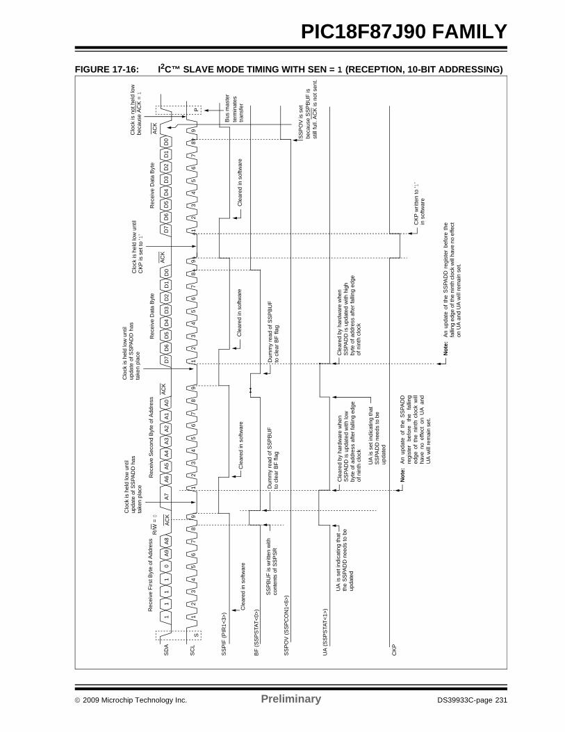
© 2009 Microchip Technology Inc. Preliminary DS39933C-page 231
PIC18F87J90 FAMILYFIGURE 17-16: I2C™ SLAVE MODE TIMING WITH SEN = 1 (RECEPTION, 10-BIT ADDRESSING)
SD
A
SC
L
SSP
IF (P
IR1<
3>)
BF
(SS
PSTA
T<0>
)
S1
23
45
67
89
12
34
56
78
91
23
45
78
9P
11
11
0A9
A8
A7A6
A5A4
A3
A2A1
A0
D7
D6
D5
D4
D3
D1
D0
Rec
eive
Dat
a B
yte
ACK
R/W
= 0
ACK
Rec
eive
Firs
t Byt
e of
Add
ress
Cle
ared
in s
oftw
are
D2 6
Cle
ared
in s
oftw
are
Rec
eive
Sec
ond
Byte
of A
ddre
ss
Cle
ared
by
hard
war
e w
hen
SSP
ADD
is u
pdat
ed w
ith lo
wby
te o
f add
ress
afte
r fal
ling
edge
UA
(SSP
STA
T<1>
)
Clo
ck is
hel
d lo
w u
ntil
upda
te o
f SS
PAD
D h
as
take
n pl
ace
UA
is s
et in
dica
ting
that
the
SSPA
DD
nee
ds to
be
upda
ted
UA
is s
et in
dica
ting
that
SSPA
DD
nee
ds to
be
upda
ted
Cle
ared
by
hard
war
e w
hen
SSPA
DD
is u
pdat
ed w
ith h
igh
byte
of a
ddre
ss a
fter f
allin
g ed
ge
SSPB
UF
is w
ritte
n w
ithco
nten
ts o
f SSP
SRD
umm
y re
ad o
f SSP
BUF
to c
lear
BF
flag
ACK
CKP
12
34
57
89
D7
D6
D5
D4
D3
D1
D0
Rec
eive
Dat
a B
yte
Bus
mas
ter
term
inat
estra
nsfe
r
D2 6
ACK
Cle
ared
in s
oftw
are
Cle
ared
in s
oftw
are
SSP
OV
(SSP
CO
N1<
6>)
CKP
writ
ten
to ‘1
’
Not
e:An
upd
ate
of th
e S
SPA
DD
reg
iste
r be
fore
the
falli
ng e
dge
of th
e ni
nth
cloc
k w
ill ha
ve n
o ef
fect
on U
A an
d U
A w
ill re
mai
n se
t.
Not
e:A
n up
date
of
the
SSP
ADD
regi
ster
be
fore
th
e fa
lling
edge
of
the
nint
h cl
ock
will
have
no
effe
ct o
n U
A an
dU
A w
ill re
mai
n se
t. in
sof
twar
e
Clo
ck is
hel
d lo
w u
ntil
upda
te o
f SSP
ADD
has
ta
ken
plac
e of n
inth
clo
ckof
nin
th c
lock
SSP
OV
is s
etbe
caus
e S
SPB
UF
isst
ill fu
ll. A
CK
is n
ot s
ent.
Dum
my
read
of S
SPB
UF
to c
lear
BF
flag
Clo
ck is
hel
d lo
w u
ntil
CKP
is s
et to
‘1’
Clo
ck is
not
hel
d lo
wbe
caus
e AC
K = 1
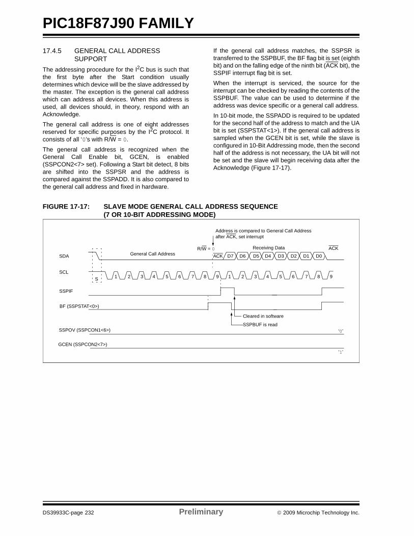
PIC18F87J90 FAMILY
DS39933C-page 232 Preliminary © 2009 Microchip Technology Inc.
17.4.5 GENERAL CALL ADDRESS SUPPORT
The addressing procedure for the I2C bus is such thatthe first byte after the Start condition usuallydetermines which device will be the slave addressed bythe master. The exception is the general call addresswhich can address all devices. When this address isused, all devices should, in theory, respond with anAcknowledge.
The general call address is one of eight addressesreserved for specific purposes by the I2C protocol. Itconsists of all ‘0’s with R/W = 0.
The general call address is recognized when theGeneral Call Enable bit, GCEN, is enabled(SSPCON2<7> set). Following a Start bit detect, 8 bitsare shifted into the SSPSR and the address iscompared against the SSPADD. It is also compared tothe general call address and fixed in hardware.
If the general call address matches, the SSPSR istransferred to the SSPBUF, the BF flag bit is set (eighthbit) and on the falling edge of the ninth bit (ACK bit), theSSPIF interrupt flag bit is set.
When the interrupt is serviced, the source for theinterrupt can be checked by reading the contents of theSSPBUF. The value can be used to determine if theaddress was device specific or a general call address.
In 10-bit mode, the SSPADD is required to be updatedfor the second half of the address to match and the UAbit is set (SSPSTAT<1>). If the general call address issampled when the GCEN bit is set, while the slave isconfigured in 10-Bit Addressing mode, then the secondhalf of the address is not necessary, the UA bit will notbe set and the slave will begin receiving data after theAcknowledge (Figure 17-17).
FIGURE 17-17: SLAVE MODE GENERAL CALL ADDRESS SEQUENCE (7 OR 10-BIT ADDRESSING MODE)
SDA
SCLS
SSPIF
BF (SSPSTAT<0>)
SSPOV (SSPCON1<6>)
Cleared in software
SSPBUF is read
R/W = 0ACKGeneral Call Address
Address is compared to General Call Address
GCEN (SSPCON2<7>)
Receiving Data ACK
1 2 3 4 5 6 7 8 9 1 2 3 4 5 6 7 8 9
D7 D6 D5 D4 D3 D2 D1 D0
after ACK, set interrupt
‘0’
‘1’
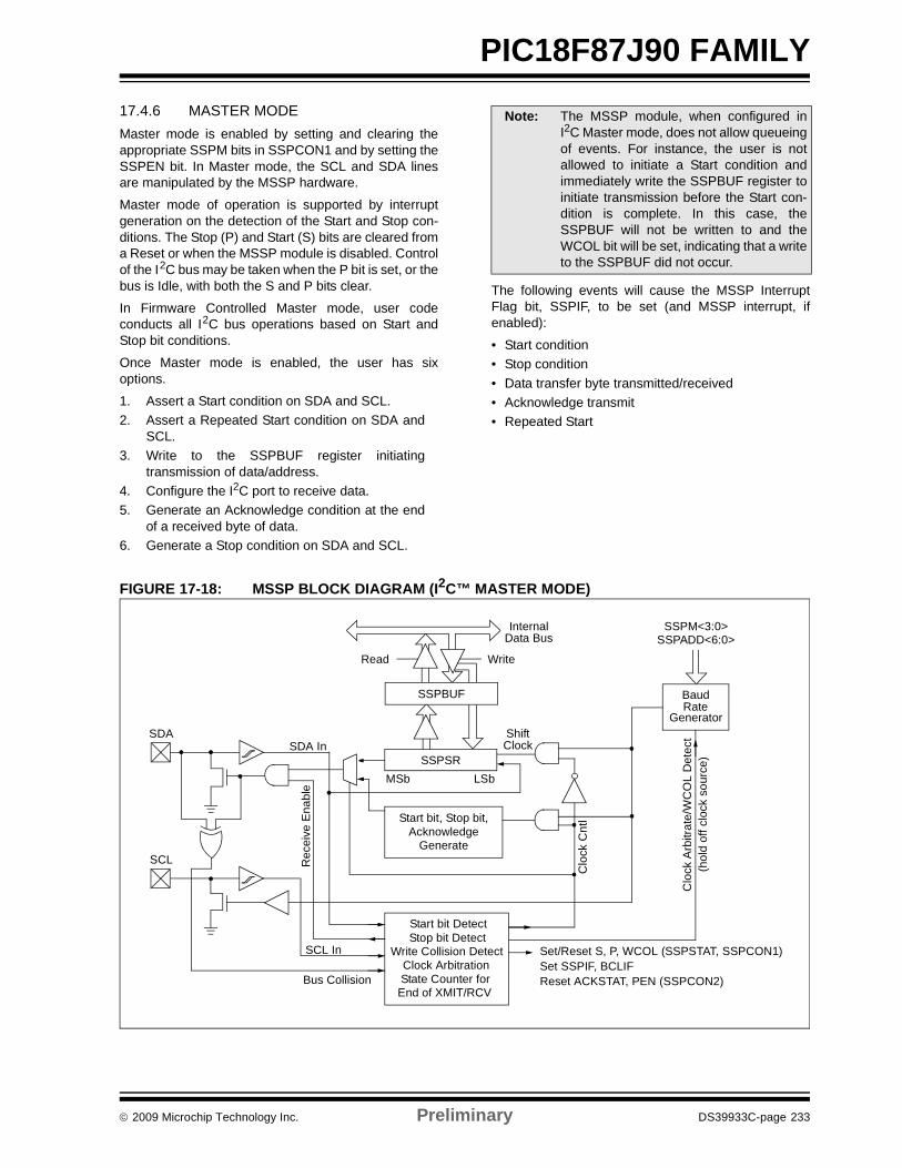
© 2009 Microchip Technology Inc. Preliminary DS39933C-page 233
PIC18F87J90 FAMILY17.4.6 MASTER MODEMaster mode is enabled by setting and clearing theappropriate SSPM bits in SSPCON1 and by setting theSSPEN bit. In Master mode, the SCL and SDA linesare manipulated by the MSSP hardware.
Master mode of operation is supported by interruptgeneration on the detection of the Start and Stop con-ditions. The Stop (P) and Start (S) bits are cleared froma Reset or when the MSSP module is disabled. Controlof the I2C bus may be taken when the P bit is set, or thebus is Idle, with both the S and P bits clear.
In Firmware Controlled Master mode, user codeconducts all I2C bus operations based on Start andStop bit conditions.
Once Master mode is enabled, the user has sixoptions.
1. Assert a Start condition on SDA and SCL.2. Assert a Repeated Start condition on SDA and
SCL.3. Write to the SSPBUF register initiating
transmission of data/address.4. Configure the I2C port to receive data.5. Generate an Acknowledge condition at the end
of a received byte of data.6. Generate a Stop condition on SDA and SCL.
The following events will cause the MSSP InterruptFlag bit, SSPIF, to be set (and MSSP interrupt, ifenabled):
• Start condition• Stop condition• Data transfer byte transmitted/received• Acknowledge transmit• Repeated Start
FIGURE 17-18: MSSP BLOCK DIAGRAM (I2C™ MASTER MODE)
Note: The MSSP module, when configured inI2C Master mode, does not allow queueingof events. For instance, the user is notallowed to initiate a Start condition andimmediately write the SSPBUF register toinitiate transmission before the Start con-dition is complete. In this case, theSSPBUF will not be written to and theWCOL bit will be set, indicating that a writeto the SSPBUF did not occur.
Read Write
SSPSR
Start bit, Stop bit,
SSPBUF
InternalData Bus
Set/Reset S, P, WCOL (SSPSTAT, SSPCON1)
ShiftClock
MSb LSb
SDA
AcknowledgeGenerate
Stop bit DetectWrite Collision Detect
Clock ArbitrationState Counter forEnd of XMIT/RCV
SCL
SCL In
Bus Collision
SDA In
Rec
eive
Ena
ble
Clo
ck C
ntl
Clo
ck A
rbitr
ate/
WC
OL
Det
ect
(hol
d of
f clo
ck s
ourc
e)
SSPADD<6:0>
Baud
Set SSPIF, BCLIFReset ACKSTAT, PEN (SSPCON2)
RateGenerator
SSPM<3:0>
Start bit Detect

PIC18F87J90 FAMILY
DS39933C-page 234 Preliminary © 2009 Microchip Technology Inc.
17.4.6.1 I2C Master Mode OperationThe master device generates all of the serial clockpulses and the Start and Stop conditions. A transfer isended with a Stop condition or with a Repeated Startcondition. Since the Repeated Start condition is alsothe beginning of the next serial transfer, the I2C bus willnot be released.
In Master Transmitter mode, serial data is outputthrough SDA, while SCL outputs the serial clock. Thefirst byte transmitted contains the slave address of thereceiving device (7 bits) and the Read/Write (R/W) bit.In this case, the R/W bit will be logic ‘0’. Serial data istransmitted 8 bits at a time. After each byte is transmit-ted, an Acknowledge bit is received. Start and Stopconditions are output to indicate the beginning and theend of a serial transfer.
In Master Receive mode, the first byte transmittedcontains the slave address of the transmitting device(7 bits) and the R/W bit. In this case, the R/W bit will belogic ‘1’. Thus, the first byte transmitted is a 7-bit slaveaddress followed by a ‘1’ to indicate the receive bit.Serial data is received via SDA, while SCL outputs theserial clock. Serial data is received 8 bits at a time. Aftereach byte is received, an Acknowledge bit is transmit-ted. Start and Stop conditions indicate the beginningand end of transmission.
The Baud Rate Generator used for the SPI modeoperation is used to set the SCL clock frequency foreither 100 kHz, 400 kHz or 1 MHz I2C operation. SeeSection 17.4.7 “Baud Rate” for more detail.
A typical transmit sequence would go as follows:
1. The user generates a Start condition by settingthe Start Enable bit, SEN (SSPCON2<0>).
2. SSPIF is set. The MSSP module will wait therequired start time before any other operationtakes place.
3. The user loads the SSPBUF with the slaveaddress to transmit.
4. Address is shifted out the SDA pin until all 8 bitsare transmitted.
5. The MSSP module shifts in the ACK bit from theslave device and writes its value into theSSPCON2 register (SSPCON2<6>).
6. The MSSP module generates an interrupt at theend of the ninth clock cycle by setting the SSPIFbit.
7. The user loads the SSPBUF with eight bits ofdata.
8. Data is shifted out the SDA pin until all 8 bits aretransmitted.
9. The MSSP module shifts in the ACK bit from theslave device and writes its value into theSSPCON2 register (SSPCON2<6>).
10. The MSSP module generates an interrupt at theend of the ninth clock cycle by setting the SSPIFbit.
11. The user generates a Stop condition by settingthe Stop Enable bit, PEN (SSPCON2<2>).
12. Interrupt is generated once the Stop condition iscomplete.
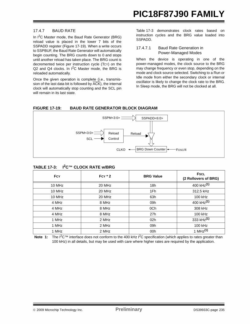
© 2009 Microchip Technology Inc. Preliminary DS39933C-page 235
PIC18F87J90 FAMILY17.4.7 BAUD RATE In I2C Master mode, the Baud Rate Generator (BRG)reload value is placed in the lower 7 bits of theSSPADD register (Figure 17-19). When a write occursto SSPBUF, the Baud Rate Generator will automaticallybegin counting. The BRG counts down to 0 and stopsuntil another reload has taken place. The BRG count isdecremented twice per instruction cycle (TCY) on theQ2 and Q4 clocks. In I2C Master mode, the BRG isreloaded automatically.
Once the given operation is complete (i.e., transmis-sion of the last data bit is followed by ACK), the internalclock will automatically stop counting and the SCL pinwill remain in its last state.
Table 17-3 demonstrates clock rates based oninstruction cycles and the BRG value loaded intoSSPADD.
17.4.7.1 Baud Rate Generation in Power-Managed Modes
When the device is operating in one of thepower-managed modes, the clock source to the BRGmay change frequency or even stop, depending on themode and clock source selected. Switching to a Run orIdle mode from either the secondary clock or internaloscillator is likely to change the clock rate to the BRG.In Sleep mode, the BRG will not be clocked at all.
FIGURE 17-19: BAUD RATE GENERATOR BLOCK DIAGRAM
TABLE 17-3: I2C™ CLOCK RATE w/BRG
FCY FCY * 2 BRG Value FSCL (2 Rollovers of BRG)
10 MHz 20 MHz 18h 400 kHz(1)
10 MHz 20 MHz 1Fh 312.5 kHz10 MHz 20 MHz 63h 100 kHz4 MHz 8 MHz 09h 400 kHz(1)
4 MHz 8 MHz 0Ch 308 kHz4 MHz 8 MHz 27h 100 kHz1 MHz 2 MHz 02h 333 kHz(1)
1 MHz 2 MHz 09h 100 kHz1 MHz 2 MHz 00h 1 MHz(1)
Note 1: The I2C™ interface does not conform to the 400 kHz I2C specification (which applies to rates greater than 100 kHz) in all details, but may be used with care where higher rates are required by the application.
SSPM<3:0>
BRG Down CounterCLKO FOSC/4
SSPADD<6:0>
SSPM<3:0>
SCL
ReloadControl
Reload
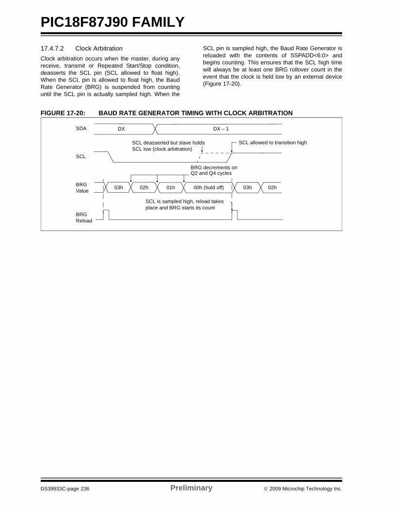
PIC18F87J90 FAMILY
DS39933C-page 236 Preliminary © 2009 Microchip Technology Inc.
17.4.7.2 Clock ArbitrationClock arbitration occurs when the master, during anyreceive, transmit or Repeated Start/Stop condition,deasserts the SCL pin (SCL allowed to float high).When the SCL pin is allowed to float high, the BaudRate Generator (BRG) is suspended from countinguntil the SCL pin is actually sampled high. When the
SCL pin is sampled high, the Baud Rate Generator isreloaded with the contents of SSPADD<6:0> andbegins counting. This ensures that the SCL high timewill always be at least one BRG rollover count in theevent that the clock is held low by an external device(Figure 17-20).
FIGURE 17-20: BAUD RATE GENERATOR TIMING WITH CLOCK ARBITRATION
SDA
SCL
SCL deasserted but slave holds
DX – 1DX
BRG
SCL is sampled high, reload takesplace and BRG starts its count
03h 02h 01h 00h (hold off) 03h 02h
Reload
BRGValue
SCL low (clock arbitration)SCL allowed to transition high
BRG decrements onQ2 and Q4 cycles
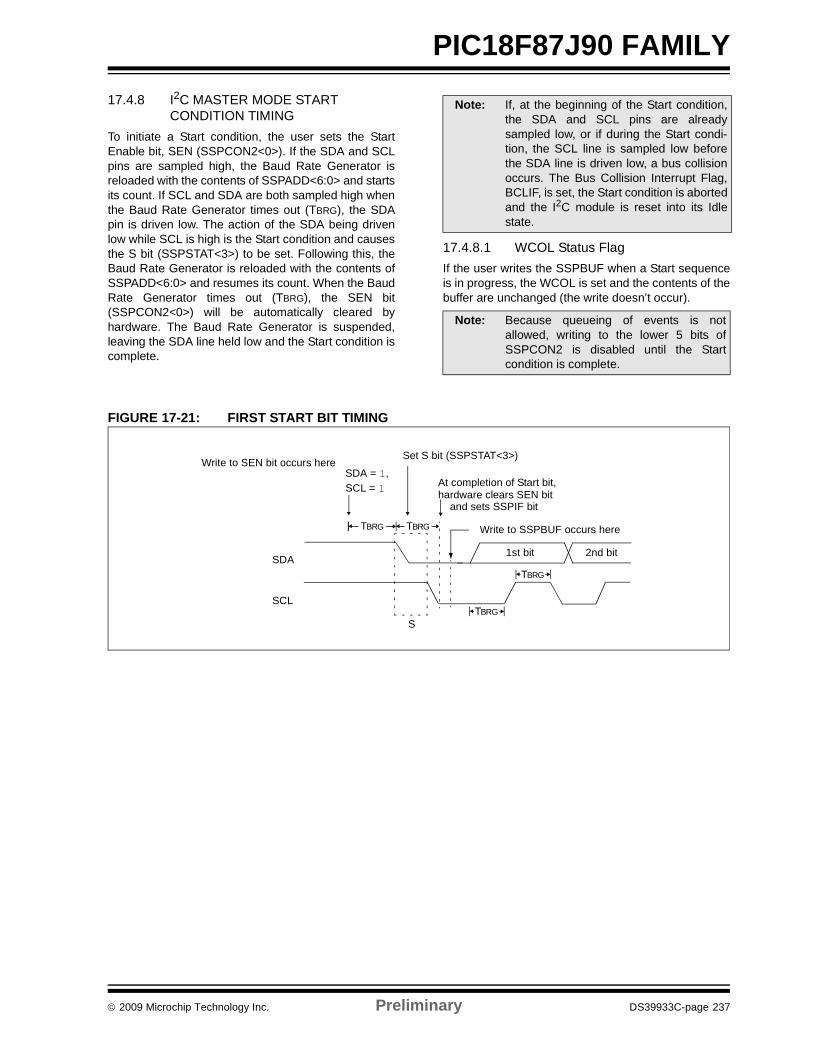
© 2009 Microchip Technology Inc. Preliminary DS39933C-page 237
PIC18F87J90 FAMILY17.4.8 I2C MASTER MODE START
CONDITION TIMINGTo initiate a Start condition, the user sets the StartEnable bit, SEN (SSPCON2<0>). If the SDA and SCLpins are sampled high, the Baud Rate Generator isreloaded with the contents of SSPADD<6:0> and startsits count. If SCL and SDA are both sampled high whenthe Baud Rate Generator times out (TBRG), the SDApin is driven low. The action of the SDA being drivenlow while SCL is high is the Start condition and causesthe S bit (SSPSTAT<3>) to be set. Following this, theBaud Rate Generator is reloaded with the contents ofSSPADD<6:0> and resumes its count. When the BaudRate Generator times out (TBRG), the SEN bit(SSPCON2<0>) will be automatically cleared byhardware. The Baud Rate Generator is suspended,leaving the SDA line held low and the Start condition iscomplete.
17.4.8.1 WCOL Status FlagIf the user writes the SSPBUF when a Start sequenceis in progress, the WCOL is set and the contents of thebuffer are unchanged (the write doesn’t occur).
FIGURE 17-21: FIRST START BIT TIMING
Note: If, at the beginning of the Start condition,the SDA and SCL pins are alreadysampled low, or if during the Start condi-tion, the SCL line is sampled low beforethe SDA line is driven low, a bus collisionoccurs. The Bus Collision Interrupt Flag,BCLIF, is set, the Start condition is abortedand the I2C module is reset into its Idlestate.
Note: Because queueing of events is notallowed, writing to the lower 5 bits ofSSPCON2 is disabled until the Startcondition is complete.
SDA
SCL
S
TBRG
1st bit 2nd bit
TBRG
SDA = 1, At completion of Start bit,SCL = 1
Write to SSPBUF occurs hereTBRG
hardware clears SEN bit
TBRG
Write to SEN bit occurs hereSet S bit (SSPSTAT<3>)
and sets SSPIF bit
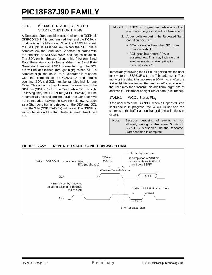
PIC18F87J90 FAMILY
DS39933C-page 238 Preliminary © 2009 Microchip Technology Inc.
17.4.9 I2C MASTER MODE REPEATED START CONDITION TIMING
A Repeated Start condition occurs when the RSEN bit(SSPCON2<1>) is programmed high and the I2C logicmodule is in the Idle state. When the RSEN bit is set,the SCL pin is asserted low. When the SCL pin issampled low, the Baud Rate Generator is loaded withthe contents of SSPADD<6:0> and begins counting.The SDA pin is released (brought high) for one BaudRate Generator count (TBRG). When the Baud RateGenerator times out, if SDA is sampled high, the SCLpin will be deasserted (brought high). When SCL issampled high, the Baud Rate Generator is reloadedwith the contents of SSPADD<6:0> and beginscounting. SDA and SCL must be sampled high for oneTBRG. This action is then followed by assertion of theSDA pin (SDA = 0) for one TBRG while SCL is high.Following this, the RSEN bit (SSPCON2<1>) will beautomatically cleared and the Baud Rate Generator willnot be reloaded, leaving the SDA pin held low. As soonas a Start condition is detected on the SDA and SCLpins, the S bit (SSPSTAT<3>) will be set. The SSPIF bitwill not be set until the Baud Rate Generator has timedout.
Immediately following the SSPIF bit getting set, the usermay write the SSPBUF with the 7-bit address in 7-bitmode or the default first address in 10-bit mode. After thefirst eight bits are transmitted and an ACK is received,the user may then transmit an additional eight bits ofaddress (10-bit mode) or eight bits of data (7-bit mode).
17.4.9.1 WCOL Status FlagIf the user writes the SSPBUF when a Repeated Startsequence is in progress, the WCOL is set and thecontents of the buffer are unchanged (the write doesn’toccur).
FIGURE 17-22: REPEATED START CONDITION WAVEFORM
Note 1: If RSEN is programmed while any otherevent is in progress, it will not take effect.
2: A bus collision during the Repeated Startcondition occurs if:
• SDA is sampled low when SCL goes from low-to-high.
• SCL goes low before SDA is asserted low. This may indicate that another master is attempting to transmit a data ‘1’.
Note: Because queueing of events is notallowed, writing of the lower 5 bits ofSSPCON2 is disabled until the RepeatedStart condition is complete.
SDA
SCL
Sr = Repeated Start
Write to SSPCON2
Write to SSPBUF occurs hereon falling edge of ninth clock,end of XMIT
At completion of Start bit, hardware clears RSEN bit
1st bit
S bit set by hardware
TBRG
TBRG
SDA = 1,SDA = 1,
SCL (no change)SCL = 1occurs here:
TBRG TBRG
and sets SSPIF
RSEN bit set by hardware
TBRG
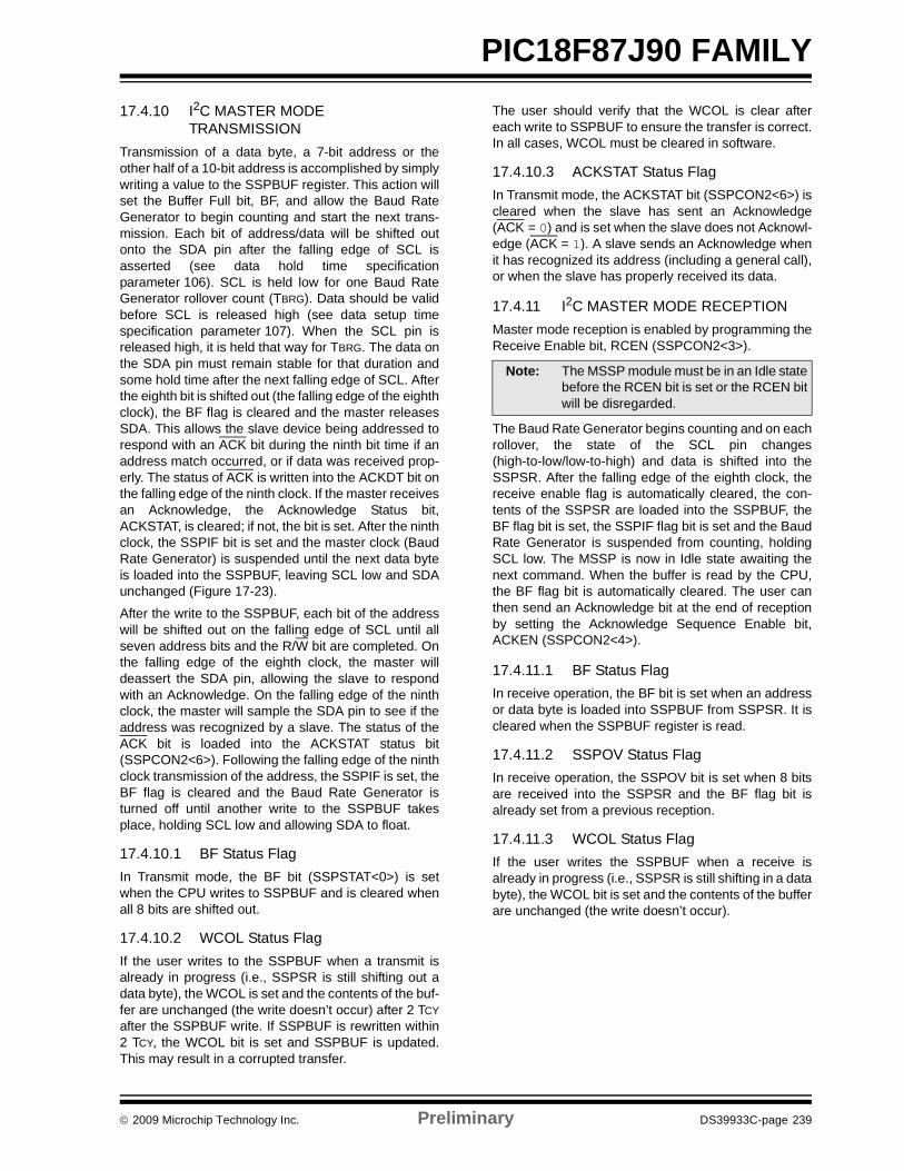
© 2009 Microchip Technology Inc. Preliminary DS39933C-page 239
PIC18F87J90 FAMILY17.4.10 I2C MASTER MODE
TRANSMISSIONTransmission of a data byte, a 7-bit address or theother half of a 10-bit address is accomplished by simplywriting a value to the SSPBUF register. This action willset the Buffer Full bit, BF, and allow the Baud RateGenerator to begin counting and start the next trans-mission. Each bit of address/data will be shifted outonto the SDA pin after the falling edge of SCL isasserted (see data hold time specificationparameter 106). SCL is held low for one Baud RateGenerator rollover count (TBRG). Data should be validbefore SCL is released high (see data setup timespecification parameter 107). When the SCL pin isreleased high, it is held that way for TBRG. The data onthe SDA pin must remain stable for that duration andsome hold time after the next falling edge of SCL. Afterthe eighth bit is shifted out (the falling edge of the eighthclock), the BF flag is cleared and the master releasesSDA. This allows the slave device being addressed torespond with an ACK bit during the ninth bit time if anaddress match occurred, or if data was received prop-erly. The status of ACK is written into the ACKDT bit onthe falling edge of the ninth clock. If the master receivesan Acknowledge, the Acknowledge Status bit,ACKSTAT, is cleared; if not, the bit is set. After the ninthclock, the SSPIF bit is set and the master clock (BaudRate Generator) is suspended until the next data byteis loaded into the SSPBUF, leaving SCL low and SDAunchanged (Figure 17-23).
After the write to the SSPBUF, each bit of the addresswill be shifted out on the falling edge of SCL until allseven address bits and the R/W bit are completed. Onthe falling edge of the eighth clock, the master willdeassert the SDA pin, allowing the slave to respondwith an Acknowledge. On the falling edge of the ninthclock, the master will sample the SDA pin to see if theaddress was recognized by a slave. The status of theACK bit is loaded into the ACKSTAT status bit(SSPCON2<6>). Following the falling edge of the ninthclock transmission of the address, the SSPIF is set, theBF flag is cleared and the Baud Rate Generator isturned off until another write to the SSPBUF takesplace, holding SCL low and allowing SDA to float.
17.4.10.1 BF Status FlagIn Transmit mode, the BF bit (SSPSTAT<0>) is setwhen the CPU writes to SSPBUF and is cleared whenall 8 bits are shifted out.
17.4.10.2 WCOL Status FlagIf the user writes to the SSPBUF when a transmit isalready in progress (i.e., SSPSR is still shifting out adata byte), the WCOL is set and the contents of the buf-fer are unchanged (the write doesn’t occur) after 2 TCYafter the SSPBUF write. If SSPBUF is rewritten within2 TCY, the WCOL bit is set and SSPBUF is updated.This may result in a corrupted transfer.
The user should verify that the WCOL is clear aftereach write to SSPBUF to ensure the transfer is correct.In all cases, WCOL must be cleared in software.
17.4.10.3 ACKSTAT Status FlagIn Transmit mode, the ACKSTAT bit (SSPCON2<6>) iscleared when the slave has sent an Acknowledge(ACK = 0) and is set when the slave does not Acknowl-edge (ACK = 1). A slave sends an Acknowledge whenit has recognized its address (including a general call),or when the slave has properly received its data.
17.4.11 I2C MASTER MODE RECEPTIONMaster mode reception is enabled by programming theReceive Enable bit, RCEN (SSPCON2<3>).
The Baud Rate Generator begins counting and on eachrollover, the state of the SCL pin changes(high-to-low/low-to-high) and data is shifted into theSSPSR. After the falling edge of the eighth clock, thereceive enable flag is automatically cleared, the con-tents of the SSPSR are loaded into the SSPBUF, theBF flag bit is set, the SSPIF flag bit is set and the BaudRate Generator is suspended from counting, holdingSCL low. The MSSP is now in Idle state awaiting thenext command. When the buffer is read by the CPU,the BF flag bit is automatically cleared. The user canthen send an Acknowledge bit at the end of receptionby setting the Acknowledge Sequence Enable bit,ACKEN (SSPCON2<4>).
17.4.11.1 BF Status FlagIn receive operation, the BF bit is set when an addressor data byte is loaded into SSPBUF from SSPSR. It iscleared when the SSPBUF register is read.
17.4.11.2 SSPOV Status FlagIn receive operation, the SSPOV bit is set when 8 bitsare received into the SSPSR and the BF flag bit isalready set from a previous reception.
17.4.11.3 WCOL Status FlagIf the user writes the SSPBUF when a receive isalready in progress (i.e., SSPSR is still shifting in a databyte), the WCOL bit is set and the contents of the bufferare unchanged (the write doesn’t occur).
Note: The MSSP module must be in an Idle statebefore the RCEN bit is set or the RCEN bitwill be disregarded.
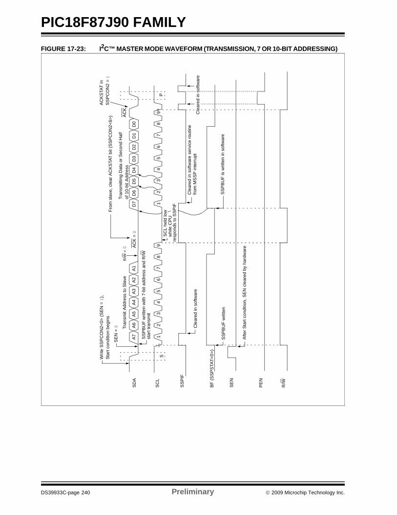
PIC18F87J90 FAMILY
DS39933C-page 240 Preliminary © 2009 Microchip Technology Inc.
FIGURE 17-23: I2C™ MASTER MODE WAVEFORM (TRANSMISSION, 7 OR 10-BIT ADDRESSING)
SD
A
SC
L
SS
PIF
BF
(SS
PS
TAT<
0>)
SE
N
A7A
6A
5A
4A
3A
2A
1A
CK
= 0
D7
D6
D5
D4
D3
D2
D1
D0
AC
KTr
ansm
ittin
g D
ata
or S
econ
d H
alf
R/W
= 0
Tran
smit
Addr
ess
to S
lave
12
34
56
78
91
23
45
67
89
P
Cle
ared
in s
oftw
are
serv
ice
rout
ine
SS
PB
UF
is w
ritte
n in
sof
twar
e
from
MS
SP
inte
rrup
t
Afte
r Sta
rt co
nditi
on, S
EN c
lear
ed b
y ha
rdw
are
S
SS
PB
UF
writ
ten
with
7-b
it ad
dres
s an
d R
/Wst
art t
rans
mit
SC
L he
ld lo
ww
hile
CP
Ure
spon
ds to
SS
PIF
SE
N =
0
of 1
0-bi
t Add
ress
Writ
e S
SP
CO
N2<
0> (S
EN =
1),
Star
t con
ditio
n be
gins
From
sla
ve, c
lear
AC
KS
TAT
bit (
SS
PC
ON
2<6>
)
AC
KS
TAT
in
SS
PC
ON
2 = 1
Cle
ared
in s
oftw
are
SSP
BU
F w
ritte
n
PE
N
R/W
Cle
ared
in s
oftw
are
© 2009 Microchip Technology Inc. Preliminary DS39933C-page 241
PIC18F87J90 FAMILYFIGURE 17-24: I2C™ MASTER MODE WAVEFORM (RECEPTION, 7-BIT ADDRESSING)
P9
87
65
D0
D1
D2
D3
D4
D5
D6
D7
S
A7
A6
A5
A4
A3
A2
A1
SD
A
SC
L1
23
45
67
89
12
34
56
78
91
23
4
Bus
mas
ter
term
inat
estra
nsfe
r
ACK
Rec
eivi
ng D
ata
from
Sla
veR
ecei
ving
Dat
a fro
m S
lave
D0
D1
D2
D3
D4
D5
D6
D7
ACK
R/W
= 1
Tran
smit
Addr
ess
to S
lave
SS
PIF
BF
AC
K is
not
sen
t
Writ
e to
SS
PCO
N2<
0> (S
EN =
1),
Writ
e to
SS
PBU
F oc
curs
her
e,AC
K fr
om S
laveM
aste
r con
figur
ed a
s a
rece
iver
by p
rogr
amm
ing
SSP
CO
N2<
3> (R
CEN
= 1
)PE
N b
it = 1
writ
ten
here
Dat
a sh
ifted
in o
n fa
lling
edge
of C
LK
Cle
ared
in s
oftw
are
star
t XM
IT
SEN
= 0
SS
PO
V
SDA
= 0
, SC
L = 1
whi
le C
PU
(SSP
STA
T<0>
)
AC
K
Cle
ared
in s
oftw
are
Cle
ared
in s
oftw
are
Set
SSP
IF in
terru
ptat
end
of r
ecei
ve
Set P
bit
(SSP
STAT
<4>)
and
SSPI
F
AC
K fro
m M
aste
r,
Set S
SPI
F at
end
Set S
SPIF
inte
rrupt
at e
nd o
f Ack
now
ledg
ese
quen
ce
Set
SSP
IF in
terru
ptat
end
of A
ckno
wle
dge
sequ
ence
of re
ceiv
e
Set A
CKE
N, s
tart
Ackn
owle
dge
sequ
ence
,S
DA
= AC
KD
T = 1
RC
EN c
lear
edau
tom
atic
ally
RC
EN =
1, s
tart
next
rece
ive
Writ
e to
SSP
CO
N2<
4>to
sta
rt Ac
know
ledg
e se
quen
ce,
SDA
= AC
KD
T (S
SPC
ON
2<5>
) = 0
RC
EN c
lear
edau
tom
atic
ally
AC
KE
Nbegi
n St
art c
ondi
tion
Cle
ared
in s
oftw
are
SDA
= A
CKD
T = 0
Last
bit
is s
hifte
d in
to S
SPSR
and
cont
ents
are
unl
oade
d in
to S
SPB
UF
Cle
ared
inso
ftwar
e
SSP
OV
is s
et b
ecau
seS
SPB
UF
is s
till f
ull
resp
onds
to S
SPI
F
PIC18F87J90 FAMILY
DS39933C-page 242 Preliminary © 2009 Microchip Technology Inc.
17.4.12 ACKNOWLEDGE SEQUENCE TIMING
An Acknowledge sequence is enabled by setting theAcknowledge Sequence Enable bit, ACKEN(SSPCON2<4>). When this bit is set, the SCL pin ispulled low and the contents of the Acknowledge data bitare presented on the SDA pin. If the user wishes to gen-erate an Acknowledge, then the ACKDT bit should becleared. If not, the user should set the ACKDT bit beforestarting an Acknowledge sequence. The Baud RateGenerator then counts for one rollover period (TBRG)and the SCL pin is deasserted (pulled high). When theSCL pin is sampled high (clock arbitration), the BaudRate Generator counts for TBRG. The SCL pin is thenpulled low. Following this, the ACKEN bit is automaticallycleared, the Baud Rate Generator is turned off and theMSSP module then goes into Idle mode (Figure 17-25).
17.4.12.1 WCOL Status FlagIf the user writes the SSPBUF when an Acknowledgesequence is in progress, then WCOL is set and thecontents of the buffer are unchanged (the write doesn’toccur).
17.4.13 STOP CONDITION TIMINGA Stop bit is asserted on the SDA pin at the end of areceive/transmit by setting the Stop Sequence Enablebit, PEN (SSPCON2<2>). At the end of areceive/transmit, the SCL line is held low after the fall-ing edge of the ninth clock. When the PEN bit is set, themaster will assert the SDA line low. When the SDA lineis sampled low, the Baud Rate Generator is reloadedand counts down to 0. When the Baud Rate Generatortimes out, the SCL pin will be brought high and oneTBRG (Baud Rate Generator rollover count) later, theSDA pin will be deasserted. When the SDA pin issampled high while SCL is high, the P bit(SSPSTAT<4>) is set. A TBRG later, the PEN bit iscleared and the SSPIF bit is set (Figure 17-26).
17.4.13.1 WCOL Status FlagIf the user writes the SSPBUF when a Stop sequenceis in progress, then the WCOL bit is set and thecontents of the buffer are unchanged (the write doesn’toccur).
FIGURE 17-25: ACKNOWLEDGE SEQUENCE WAVEFORM
FIGURE 17-26: STOP CONDITION RECEIVE OR TRANSMIT MODE
Note: TBRG = one Baud Rate Generator period.
SDA
SCL
SSPIF set at
Acknowledge sequence starts here,write to SSPCON2, ACKEN automatically cleared
Cleared in
TBRG TBRG
the end of receive
8
ACKEN = 1, ACKDT = 0
D0
9
SSPIF
software SSPIF set at the endof Acknowledge sequence
Cleared insoftware
ACK
SCL
SDA
SDA asserted low before rising edge of clock
Write to SSPCON2,set PEN
Falling edge of
SCL = 1 for TBRG, followed by SDA = 1 for TBRG
9th clock
SCL brought high after TBRG
Note: TBRG = one Baud Rate Generator period.
TBRG TBRG
after SDA sampled high. P bit (SSPSTAT<4>) is set.
TBRG
to setup Stop condition
ACK
PTBRG
PEN bit (SSPCON2<2>) is cleared byhardware and the SSPIF bit is set
© 2009 Microchip Technology Inc. Preliminary DS39933C-page 243
PIC18F87J90 FAMILY17.4.14 SLEEP OPERATIONWhile in Sleep mode, the I2C module can receiveaddresses or data and when an address match orcomplete byte transfer occurs, wake the processorfrom Sleep (if the MSSP interrupt is enabled).
17.4.15 EFFECTS OF A RESETA Reset disables the MSSP module and terminates thecurrent transfer.
17.4.16 MULTI-MASTER MODEIn Multi-Master mode, the interrupt generation on thedetection of the Start and Stop conditions allows thedetermination of when the bus is free. The Stop (P) andStart (S) bits are cleared from a Reset or when theMSSP module is disabled. Control of the I2C bus maybe taken when the P bit (SSPSTAT<4>) is set, or thebus is Idle, with both the S and P bits clear. When thebus is busy, enabling the MSSP interrupt will generatethe interrupt when the Stop condition occurs.
In multi-master operation, the SDA line must bemonitored for arbitration to see if the signal level is theexpected output level. This check is performed inhardware with the result placed in the BCLIF bit.
The states where arbitration can be lost are:
• Address Transfer • Data Transfer• A Start Condition • A Repeated Start Condition• An Acknowledge Condition
17.4.17 MULTI -MASTER COMMUNICATION, BUS COLLISION AND BUS ARBITRATION
Multi-Master mode support is achieved by bus arbitra-tion. When the master outputs address/data bits ontothe SDA pin, arbitration takes place when the masteroutputs a ‘1’ on SDA by letting SDA float high, andanother master asserts a ‘0’. When the SCL pin floatshigh, data should be stable. If the expected data onSDA is a ‘1’ and the data sampled on the SDA pin = 0,then a bus collision has taken place. The master will setthe Bus Collision Interrupt Flag, BCLIF and reset theI2C port to its Idle state (Figure 17-27).
If a transmit was in progress when the bus collisionoccurred, the transmission is halted, the BF flag iscleared, the SDA and SCL lines are deasserted and theSSPBUF can be written to. When the user services thebus collision Interrupt Service Routine and if the I2C busis free, the user can resume communication by assertinga Start condition.
If a Start, Repeated Start, Stop or Acknowledge conditionwas in progress when the bus collision occurred, thecondition is aborted, the SDA and SCL lines aredeasserted and the respective control bits in theSSPCON2 register are cleared. When the user servicesthe bus collision Interrupt Service Routine and if the I2Cbus is free, the user can resume communication byasserting a Start condition.
The master will continue to monitor the SDA and SCLpins. If a Stop condition occurs, the SSPIF bit will be set.
A write to the SSPBUF will start the transmission ofdata at the first data bit regardless of where thetransmitter left off when the bus collision occurred.
In Multi-Master mode, the interrupt generation on thedetection of Start and Stop conditions allows the deter-mination of when the bus is free. Control of the I2C buscan be taken when the P bit is set in the SSPSTATregister, or the bus is Idle and the S and P bits arecleared.
FIGURE 17-27: BUS COLLISION TIMING FOR TRANSMIT AND ACKNOWLEDGE
SDA
SCL
BCLIF
SDA released
SDA line pulled lowby another source
Sample SDA. While SCL is high,data doesn’t match what is driven
Bus collision has occurred.
Set bus collisioninterrupt (BCLIF)
by the master.
by master
Data changeswhile SCL = 0
PIC18F87J90 FAMILY
DS39933C-page 244 Preliminary © 2009 Microchip Technology Inc.
17.4.17.1 Bus Collision During a Start Condition
During a Start condition, a bus collision occurs if:
a) SDA or SCL are sampled low at the beginning ofthe Start condition (Figure 17-28).
b) SCL is sampled low before SDA is asserted low(Figure 17-29).
During a Start condition, both the SDA and the SCLpins are monitored.
If the SDA pin is already low, or the SCL pin is alreadylow, then all of the following occur:• the Start condition is aborted; • the BCLIF flag is set; and• the MSSP module is reset to its Idle state
(Figure 17-28).
The Start condition begins with the SDA and SCL pinsdeasserted. When the SDA pin is sampled high, theBaud Rate Generator is loaded from SSPADD<6:0>and counts down to 0. If the SCL pin is sampled lowwhile SDA is high, a bus collision occurs, because it isassumed that another master is attempting to drive adata ‘1’ during the Start condition.
If the SDA pin is sampled low during this count, theBRG is reset and the SDA line is asserted early(Figure 17-30). If, however, a ‘1’ is sampled on the SDApin, the SDA pin is asserted low at the end of the BRGcount. The Baud Rate Generator is then reloaded andcounts down to 0. If the SCL pin is sampled as ‘0’during this time, a bus collision does not occur. At theend of the BRG count, the SCL pin is asserted low.
FIGURE 17-28: BUS COLLISION DURING START CONDITION (SDA ONLY)
Note: The reason that bus collision is not a factorduring a Start condition is that no two busmasters can assert a Start condition at theexact same time. Therefore, one masterwill always assert SDA before the other.This condition does not cause a bus colli-sion because the two masters must beallowed to arbitrate the first addressfollowing the Start condition. If the addressis the same, arbitration must be allowed tocontinue into the data portion, RepeatedStart or Stop conditions.
SDA
SCL
SEN
SDA sampled low before
SDA goes low before the SEN bit is set.
S bit and SSPIF set because
MSSP module reset into Idle state.SEN cleared automatically because of bus collision.
S bit and SSPIF set because
Set SEN, enable Startcondition if SDA = 1, SCL = 1
SDA = 0, SCL = 1.
BCLIF
SSPIF
SDA = 0, SCL = 1.
SSPIF and BCLIF arecleared in software
SSPIF and BCLIF arecleared in software
Set BCLIF,
Start condition. Set BCLIF.
S
© 2009 Microchip Technology Inc. Preliminary DS39933C-page 245
PIC18F87J90 FAMILYFIGURE 17-29: BUS COLLISION DURING START CONDITION (SCL = 0)
FIGURE 17-30: BRG RESET DUE TO SDA ARBITRATION DURING START CONDITION
SDA
SCL
SENbus collision occurs. Set BCLIF.SCL = 0 before SDA = 0,
Set SEN, enable Startsequence if SDA = 1, SCL = 1
TBRG TBRG
SDA = 0, SCL = 1
BCLIF
S
SSPIF
Interrupt clearedin software
bus collision occurs. Set BCLIF.SCL = 0 before BRG time-out,
‘0’ ‘0’
‘0’‘0’
SDA
SCL
SEN
Set SLess than TBRG TBRG
SDA = 0, SCL = 1
BCLIF
S
SSPIF
S
Interrupts clearedin softwareset SSPIF
SDA = 0, SCL = 1,
SCL pulled low after BRGtime-out
Set SSPIF
‘0’
SDA pulled low by other master.Reset BRG and assert SDA.
Set SEN, enable Startsequence if SDA = 1, SCL = 1
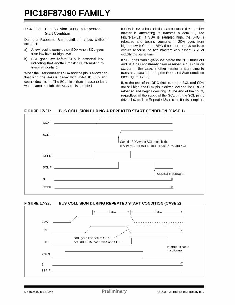
PIC18F87J90 FAMILY
DS39933C-page 246 Preliminary © 2009 Microchip Technology Inc.
17.4.17.2 Bus Collision During a Repeated Start Condition
During a Repeated Start condition, a bus collisionoccurs if:
a) A low level is sampled on SDA when SCL goesfrom low level to high level.
b) SCL goes low before SDA is asserted low,indicating that another master is attempting totransmit a data ‘1’.
When the user deasserts SDA and the pin is allowed tofloat high, the BRG is loaded with SSPADD<6:0> andcounts down to ‘0’. The SCL pin is then deasserted andwhen sampled high, the SDA pin is sampled.
If SDA is low, a bus collision has occurred (i.e., anothermaster is attempting to transmit a data ‘0’, seeFigure 17-31). If SDA is sampled high, the BRG isreloaded and begins counting. If SDA goes fromhigh-to-low before the BRG times out, no bus collisionoccurs because no two masters can assert SDA atexactly the same time.
If SCL goes from high-to-low before the BRG times outand SDA has not already been asserted, a bus collisionoccurs. In this case, another master is attempting totransmit a data ‘1’ during the Repeated Start condition(see Figure 17-32).
If, at the end of the BRG time-out, both SCL and SDAare still high, the SDA pin is driven low and the BRG isreloaded and begins counting. At the end of the count,regardless of the status of the SCL pin, the SCL pin isdriven low and the Repeated Start condition is complete.
FIGURE 17-31: BUS COLLISION DURING A REPEATED START CONDITION (CASE 1)
FIGURE 17-32: BUS COLLISION DURING REPEATED START CONDITION (CASE 2)
SDA
SCL
RSEN
BCLIF
S
SSPIF
Sample SDA when SCL goes high.If SDA = 0, set BCLIF and release SDA and SCL.
Cleared in software
‘0’
‘0’
SDA
SCL
BCLIF
RSEN
S
SSPIF
Interrupt clearedin software
SCL goes low before SDA,set BCLIF. Release SDA and SCL.
TBRG TBRG
‘0’
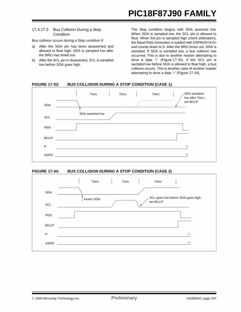
© 2009 Microchip Technology Inc. Preliminary DS39933C-page 247
PIC18F87J90 FAMILY17.4.17.3 Bus Collision During a Stop
ConditionBus collision occurs during a Stop condition if:
a) After the SDA pin has been deasserted andallowed to float high, SDA is sampled low afterthe BRG has timed out.
b) After the SCL pin is deasserted, SCL is sampledlow before SDA goes high.
The Stop condition begins with SDA asserted low.When SDA is sampled low, the SCL pin is allowed tofloat. When the pin is sampled high (clock arbitration),the Baud Rate Generator is loaded with SSPADD<6:0>and counts down to 0. After the BRG times out, SDA issampled. If SDA is sampled low, a bus collision hasoccurred. This is due to another master attempting todrive a data ‘0’ (Figure 17-33). If the SCL pin issampled low before SDA is allowed to float high, a buscollision occurs. This is another case of another masterattempting to drive a data ‘0’ (Figure 17-34).
FIGURE 17-33: BUS COLLISION DURING A STOP CONDITION (CASE 1)
FIGURE 17-34: BUS COLLISION DURING A STOP CONDITION (CASE 2)
SDA
SCL
BCLIF
PEN
P
SSPIF
TBRG TBRG TBRG
SDA asserted low
SDA sampledlow after TBRG,set BCLIF
‘0’
‘0’
SDA
SCL
BCLIF
PEN
P
SSPIF
TBRG TBRG TBRG
Assert SDA SCL goes low before SDA goes high,set BCLIF
‘0’
‘0’
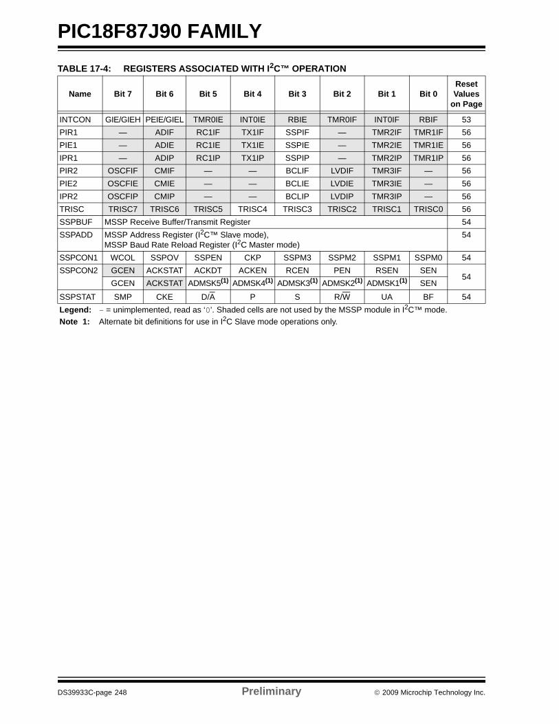
PIC18F87J90 FAMILY
DS39933C-page 248 Preliminary © 2009 Microchip Technology Inc.
TABLE 17-4: REGISTERS ASSOCIATED WITH I2C™ OPERATION
Name Bit 7 Bit 6 Bit 5 Bit 4 Bit 3 Bit 2 Bit 1 Bit 0Reset Values
on Page
INTCON GIE/GIEH PEIE/GIEL TMR0IE INT0IE RBIE TMR0IF INT0IF RBIF 53PIR1 — ADIF RC1IF TX1IF SSPIF — TMR2IF TMR1IF 56PIE1 — ADIE RC1IE TX1IE SSPIE — TMR2IE TMR1IE 56IPR1 — ADIP RC1IP TX1IP SSPIP — TMR2IP TMR1IP 56PIR2 OSCFIF CMIF — — BCLIF LVDIF TMR3IF — 56PIE2 OSCFIE CMIE — — BCLIE LVDIE TMR3IE — 56IPR2 OSCFIP CMIP — — BCLIP LVDIP TMR3IP — 56TRISC TRISC7 TRISC6 TRISC5 TRISC4 TRISC3 TRISC2 TRISC1 TRISC0 56SSPBUF MSSP Receive Buffer/Transmit Register 54SSPADD MSSP Address Register (I2C™ Slave mode),
MSSP Baud Rate Reload Register (I2C Master mode)54
SSPCON1 WCOL SSPOV SSPEN CKP SSPM3 SSPM2 SSPM1 SSPM0 54SSPCON2 GCEN ACKSTAT ACKDT ACKEN RCEN PEN RSEN SEN
54GCEN ACKSTAT ADMSK5(1) ADMSK4(1) ADMSK3(1) ADMSK2(1) ADMSK1(1) SEN
SSPSTAT SMP CKE D/A P S R/W UA BF 54Legend: — = unimplemented, read as ‘0’. Shaded cells are not used by the MSSP module in I2C™ mode.Note 1: Alternate bit definitions for use in I2C Slave mode operations only.
© 2009 Microchip Technology Inc. Preliminary DS39933C-page 249
PIC18F87J90 FAMILY
18.0 ENHANCED UNIVERSAL SYNCHRONOUS ASYNCHRONOUS RECEIVER TRANSMITTER (EUSART)
PIC18F87J90 family devices have three serial I/Omodules: the MSSP module, discussed in the previouschapter and two Universal Synchronous AsynchronousReceiver Transmitter (USART) modules. (Generically,the USART is also known as a Serial CommunicationsInterface or SCI.) The USART can be configured as afull-duplex asynchronous system that can communi-cate with peripheral devices, such as CRT terminalsand personal computers. It can also be configured as ahalf-duplex synchronous system that can communicatewith peripheral devices, such as A/D or D/A integratedcircuits, serial EEPROMs, etc.
There are two distinct implementations of the USARTmodule in these devices: the Enhanced USART(EUSART) discussed here and the AddressableUSART discussed in the next chapter. For this devicefamily, USART1 always refers to the EUSART, whileUSART2 is always the AUSART.
The EUSART and AUSART modules implement thesame core features for serial communications; theirbasic operation is essentially the same. The EUSARTmodule provides additional features, including Auto-matic Baud Rate Detection and calibration, automaticwake-up on Sync Break reception and 12-bit Breakcharacter transmit. These features make it ideallysuited for use in Local Interconnect Network bus (LINbus) systems.
The EUSART can be configured in the followingmodes:
• Asynchronous (full-duplex) with:- Auto-wake-up on character reception- Auto-baud calibration- 12-bit Break character transmission
• Synchronous – Master (half-duplex) with selectable clock polarity
• Synchronous – Slave (half-duplex) with selectable clock polarity
The pins of the EUSART are multiplexed with thefunctions of PORTC (RC6/TX1/CK1/SEG27 andRC7/RX1/DT1/SEG28). In order to configure thesepins as an EUSART:
• bit SPEN (RCSTA1<7>) must be set (= 1)• bit TRISC<7> must be set (= 1)• bit TRISC<6> must be set (= 1)
The driver for the TX1 output pin can also be optionallyconfigured as an open-drain output. This feature allowsthe voltage level on the pin to be pulled to a higher levelthrough an external pull-up resistor, and allows the out-put to communicate with external circuits without theneed for additional level shifters.
The open-drain output option is controlled by the U1ODbit (LATG<6>). Setting the bit configures the pin foropen-drain operation.
18.1 Control RegistersThe operation of the Enhanced USART module iscontrolled through three registers:
• Transmit Status and Control Register 1 (TXSTA1)• Receive Status and Control Register 1 (RCSTA1)• Baud Rate Control Register 1 (BAUDCON1)
The registers are described in Register 18-1,Register 18-2 and Register 18-3.
Note: The EUSART control will automaticallyreconfigure the pin from input to output asneeded.
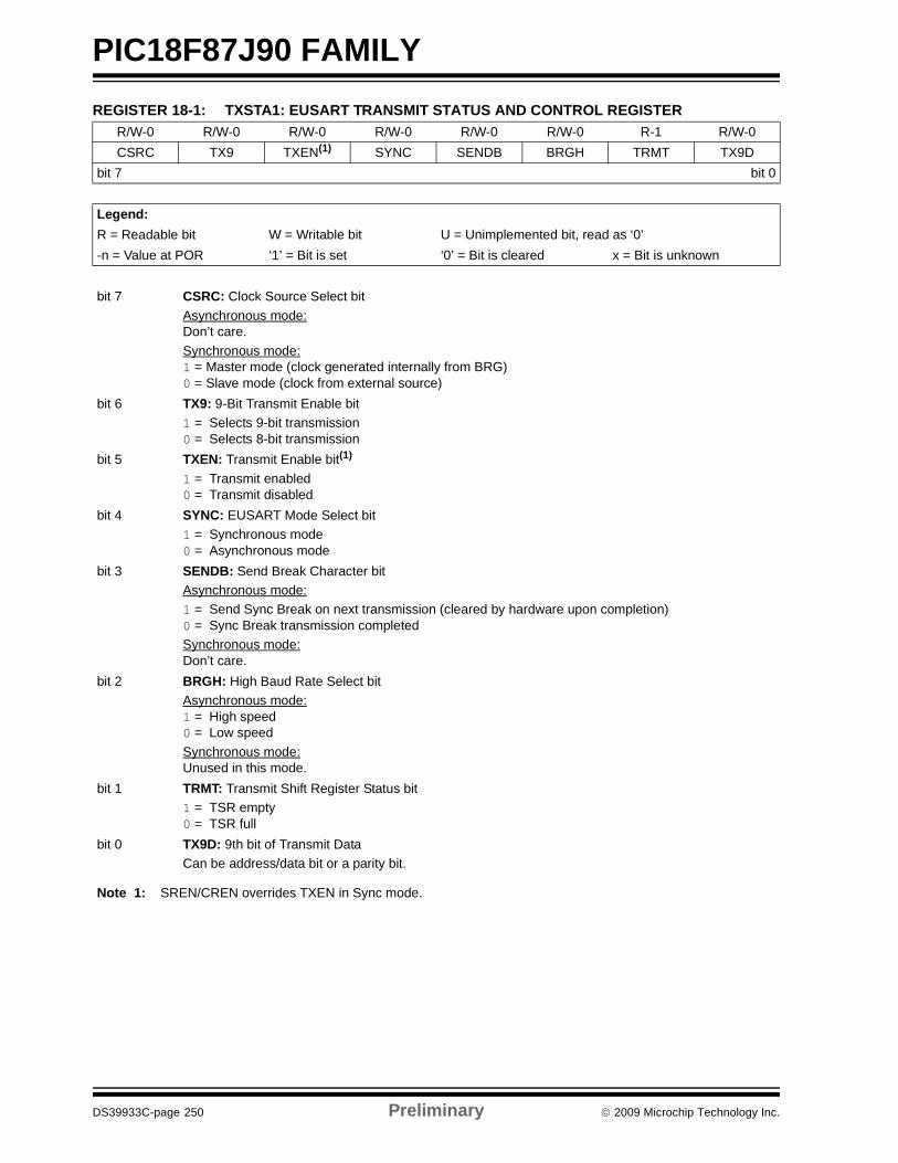
PIC18F87J90 FAMILY
DS39933C-page 250 Preliminary © 2009 Microchip Technology Inc.
REGISTER 18-1: TXSTA1: EUSART TRANSMIT STATUS AND CONTROL REGISTER R/W-0 R/W-0 R/W-0 R/W-0 R/W-0 R/W-0 R-1 R/W-0CSRC TX9 TXEN(1) SYNC SENDB BRGH TRMT TX9D
bit 7 bit 0
Legend:R = Readable bit W = Writable bit U = Unimplemented bit, read as ‘0’-n = Value at POR ‘1’ = Bit is set ‘0’ = Bit is cleared x = Bit is unknown
bit 7 CSRC: Clock Source Select bitAsynchronous mode: Don’t care.Synchronous mode: 1 = Master mode (clock generated internally from BRG)0 = Slave mode (clock from external source)
bit 6 TX9: 9-Bit Transmit Enable bit 1 = Selects 9-bit transmission 0 = Selects 8-bit transmission
bit 5 TXEN: Transmit Enable bit(1) 1 = Transmit enabled0 = Transmit disabled
bit 4 SYNC: EUSART Mode Select bit 1 = Synchronous mode 0 = Asynchronous mode
bit 3 SENDB: Send Break Character bitAsynchronous mode:1 = Send Sync Break on next transmission (cleared by hardware upon completion)0 = Sync Break transmission completedSynchronous mode:Don’t care.
bit 2 BRGH: High Baud Rate Select bit Asynchronous mode: 1 = High speed 0 = Low speedSynchronous mode: Unused in this mode.
bit 1 TRMT: Transmit Shift Register Status bit1 = TSR empty 0 = TSR full
bit 0 TX9D: 9th bit of Transmit DataCan be address/data bit or a parity bit.
Note 1: SREN/CREN overrides TXEN in Sync mode.
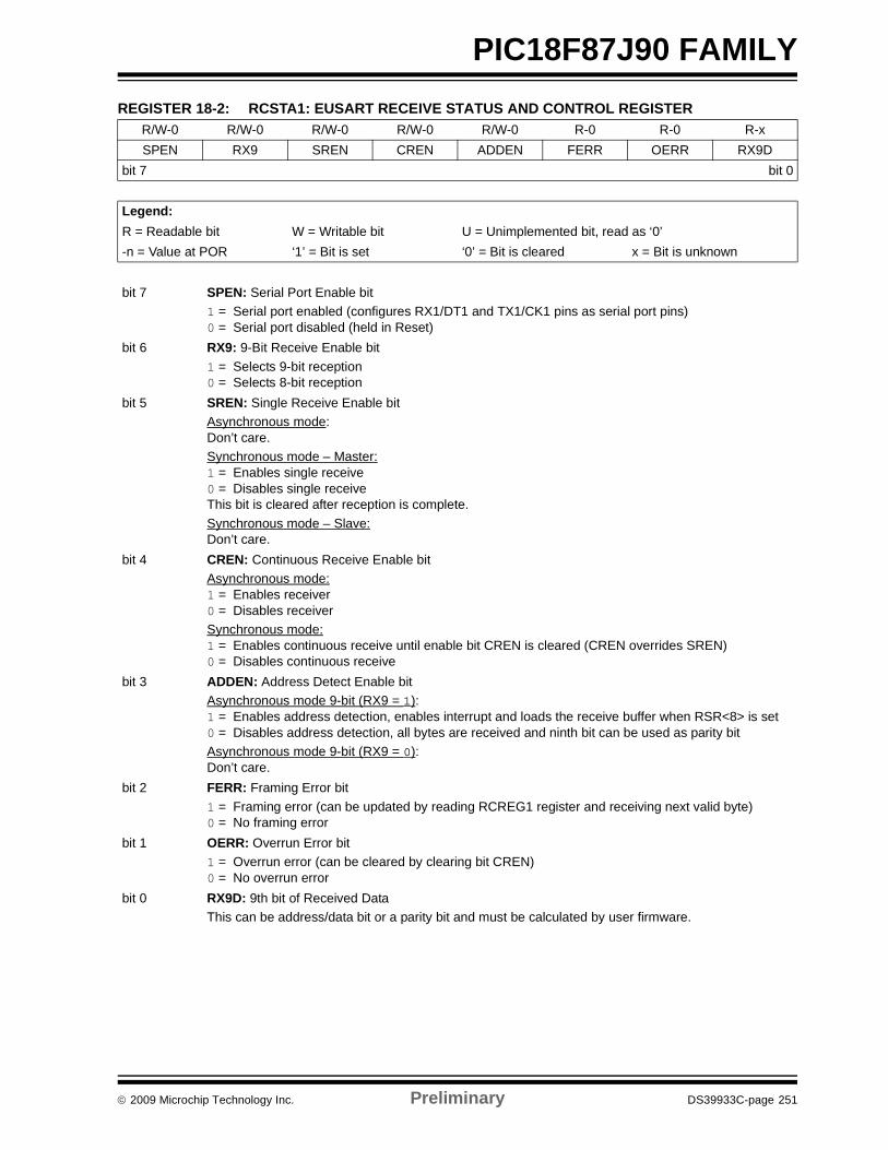
© 2009 Microchip Technology Inc. Preliminary DS39933C-page 251
PIC18F87J90 FAMILYREGISTER 18-2: RCSTA1: EUSART RECEIVE STATUS AND CONTROL REGISTER
R/W-0 R/W-0 R/W-0 R/W-0 R/W-0 R-0 R-0 R-xSPEN RX9 SREN CREN ADDEN FERR OERR RX9D
bit 7 bit 0
Legend:R = Readable bit W = Writable bit U = Unimplemented bit, read as ‘0’-n = Value at POR ‘1’ = Bit is set ‘0’ = Bit is cleared x = Bit is unknown
bit 7 SPEN: Serial Port Enable bit1 = Serial port enabled (configures RX1/DT1 and TX1/CK1 pins as serial port pins)0 = Serial port disabled (held in Reset)
bit 6 RX9: 9-Bit Receive Enable bit1 = Selects 9-bit reception 0 = Selects 8-bit reception
bit 5 SREN: Single Receive Enable bit Asynchronous mode: Don’t care.Synchronous mode – Master: 1 = Enables single receive0 = Disables single receive This bit is cleared after reception is complete.Synchronous mode – Slave: Don’t care.
bit 4 CREN: Continuous Receive Enable bit Asynchronous mode: 1 = Enables receiver0 = Disables receiverSynchronous mode: 1 = Enables continuous receive until enable bit CREN is cleared (CREN overrides SREN) 0 = Disables continuous receive
bit 3 ADDEN: Address Detect Enable bitAsynchronous mode 9-bit (RX9 = 1):1 = Enables address detection, enables interrupt and loads the receive buffer when RSR<8> is set0 = Disables address detection, all bytes are received and ninth bit can be used as parity bitAsynchronous mode 9-bit (RX9 = 0):Don’t care.
bit 2 FERR: Framing Error bit 1 = Framing error (can be updated by reading RCREG1 register and receiving next valid byte)0 = No framing error
bit 1 OERR: Overrun Error bit 1 = Overrun error (can be cleared by clearing bit CREN) 0 = No overrun error
bit 0 RX9D: 9th bit of Received Data This can be address/data bit or a parity bit and must be calculated by user firmware.
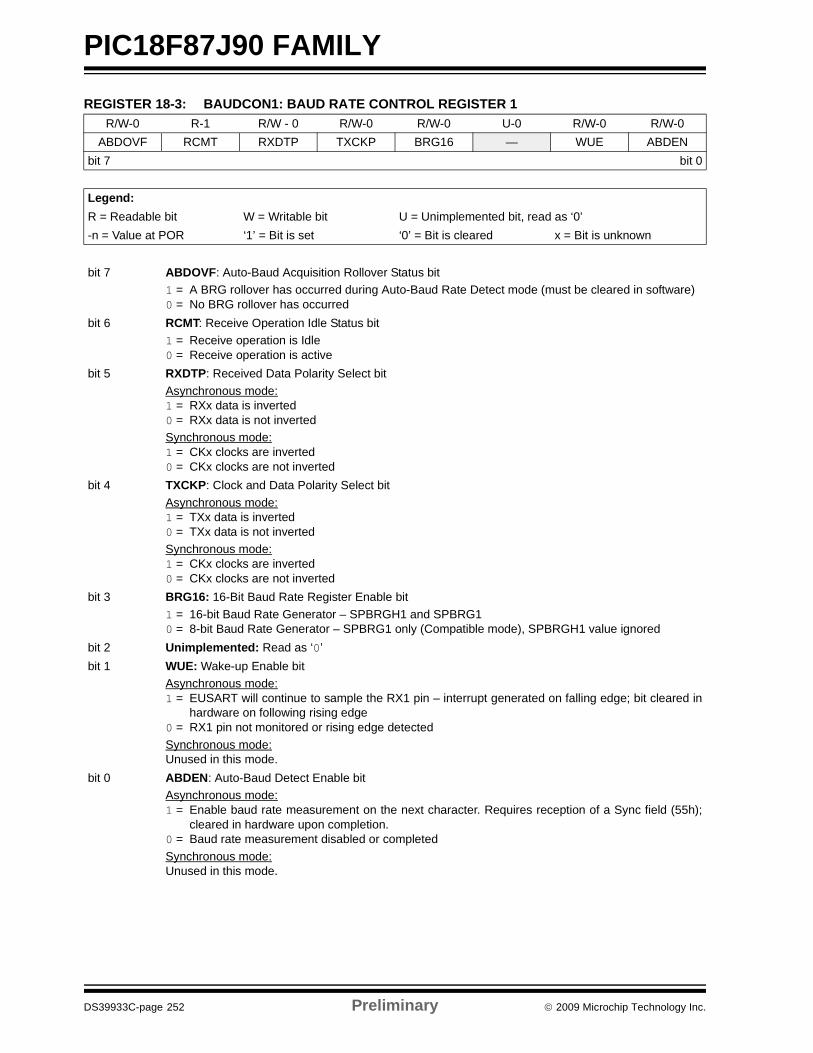
PIC18F87J90 FAMILY
DS39933C-page 252 Preliminary © 2009 Microchip Technology Inc.
REGISTER 18-3: BAUDCON1: BAUD RATE CONTROL REGISTER 1R/W-0 R-1 R/W - 0 R/W-0 R/W-0 U-0 R/W-0 R/W-0
ABDOVF RCMT RXDTP TXCKP BRG16 — WUE ABDENbit 7 bit 0
Legend:R = Readable bit W = Writable bit U = Unimplemented bit, read as ‘0’-n = Value at POR ‘1’ = Bit is set ‘0’ = Bit is cleared x = Bit is unknown
bit 7 ABDOVF: Auto-Baud Acquisition Rollover Status bit1 = A BRG rollover has occurred during Auto-Baud Rate Detect mode (must be cleared in software)0 = No BRG rollover has occurred
bit 6 RCMT: Receive Operation Idle Status bit1 = Receive operation is Idle0 = Receive operation is active
bit 5 RXDTP: Received Data Polarity Select bitAsynchronous mode:1 = RXx data is inverted0 = RXx data is not invertedSynchronous mode:1 = CKx clocks are inverted0 = CKx clocks are not inverted
bit 4 TXCKP: Clock and Data Polarity Select bitAsynchronous mode:1 = TXx data is inverted0 = TXx data is not invertedSynchronous mode:1 = CKx clocks are inverted0 = CKx clocks are not inverted
bit 3 BRG16: 16-Bit Baud Rate Register Enable bit1 = 16-bit Baud Rate Generator – SPBRGH1 and SPBRG10 = 8-bit Baud Rate Generator – SPBRG1 only (Compatible mode), SPBRGH1 value ignored
bit 2 Unimplemented: Read as ‘0’bit 1 WUE: Wake-up Enable bit
Asynchronous mode:1 = EUSART will continue to sample the RX1 pin – interrupt generated on falling edge; bit cleared in
hardware on following rising edge0 = RX1 pin not monitored or rising edge detectedSynchronous mode:Unused in this mode.
bit 0 ABDEN: Auto-Baud Detect Enable bitAsynchronous mode:1 = Enable baud rate measurement on the next character. Requires reception of a Sync field (55h);
cleared in hardware upon completion.0 = Baud rate measurement disabled or completedSynchronous mode:Unused in this mode.
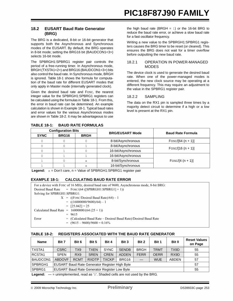
© 2009 Microchip Technology Inc. Preliminary DS39933C-page 253
PIC18F87J90 FAMILY18.2 EUSART Baud Rate Generator
(BRG)The BRG is a dedicated, 8-bit or 16-bit generator thatsupports both the Asynchronous and Synchronousmodes of the EUSART. By default, the BRG operatesin 8-bit mode; setting the BRG16 bit (BAUDCON1<3>)selects 16-bit mode.The SPBRGH1:SPBRG1 register pair controls theperiod of a free-running timer. In Asynchronous mode,BRGH (TXSTA1<2>) and BRG16 (BAUDCON1<3>) bitsalso control the baud rate. In Synchronous mode, BRGHis ignored. Table 18-1 shows the formula for computa-tion of the baud rate for different EUSART modes thatonly apply in Master mode (internally generated clock).Given the desired baud rate and FOSC, the nearestinteger value for the SPBRGH1:SPBRG1 registers canbe calculated using the formulas in Table 18-1. From this,the error in baud rate can be determined. An examplecalculation is shown in Example 18-1. Typical baud ratesand error values for the various Asynchronous modesare shown in Table 18-2. It may be advantageous to use
the high baud rate (BRGH = 1) or the 16-bit BRG toreduce the baud rate error, or achieve a slow baud ratefor a fast oscillator frequency.Writing a new value to the SPBRGH1:SPBRG1 regis-ters causes the BRG timer to be reset (or cleared). Thisensures the BRG does not wait for a timer overflowbefore outputting the new baud rate.
18.2.1 OPERATION IN POWER-MANAGED MODES
The device clock is used to generate the desired baudrate. When one of the power-managed modes isentered, the new clock source may be operating at adifferent frequency. This may require an adjustment tothe value in the SPBRG1 register pair.
18.2.2 SAMPLINGThe data on the RX1 pin is sampled three times by amajority detect circuit to determine if a high or a lowlevel is present at the RX1 pin.
TABLE 18-1: BAUD RATE FORMULAS
EXAMPLE 18-1: CALCULATING BAUD RATE ERROR
TABLE 18-2: REGISTERS ASSOCIATED WITH THE BAUD RATE GENERATOR
Configuration BitsBRG/EUSART Mode Baud Rate Formula
SYNC BRG16 BRGH0 0 0 8-bit/Asynchronous FOSC/[64 (n + 1)]0 0 1 8-bit/Asynchronous
FOSC/[16 (n + 1)]0 1 0 16-bit/Asynchronous0 1 1 16-bit/Asynchronous
FOSC/[4 (n + 1)]1 0 x 8-bit/Synchronous1 1 x 16-bit/Synchronous
Legend: x = Don’t care, n = Value of SPBRGH1:SPBRG1 register pair
Name Bit 7 Bit 6 Bit 5 Bit 4 Bit 3 Bit 2 Bit 1 Bit 0 Reset Values on Page
TXSTA1 CSRC TX9 TXEN SYNC SENDB BRGH TRMT TX9D 55RCSTA1 SPEN RX9 SREN CREN ADDEN FERR OERR RX9D 55BAUDCON1 ABDOVF RCMT RXDTP TXCKP BRG16 — WUE ABDEN 57SPBRGH1 EUSART Baud Rate Generator Register High Byte 57SPBRG1 EUSART Baud Rate Generator Register Low Byte 55Legend: — = unimplemented, read as ‘0’. Shaded cells are not used by the BRG.
For a device with FOSC of 16 MHz, desired baud rate of 9600, Asynchronous mode, 8-bit BRG:Desired Baud Rate = FOSC/(64 ([SPBRGH1:SPBRG1] + 1)) Solving for SPBRGH1:SPBRG1:
X = ((FOSC/Desired Baud Rate)/64) – 1= ((16000000/9600)/64) – 1 = [25.042] = 25
Calculated Baud Rate = 16000000/(64 (25 + 1)) = 9615
Error = (Calculated Baud Rate – Desired Baud Rate)/Desired Baud Rate= (9615 – 9600)/9600 = 0.16%
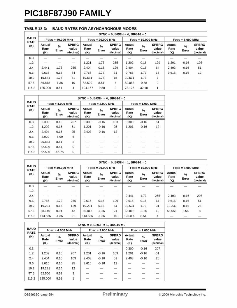
PIC18F87J90 FAMILY
DS39933C-page 254 Preliminary © 2009 Microchip Technology Inc.
TABLE 18-3: BAUD RATES FOR ASYNCHRONOUS MODES
BAUDRATE
(K)
SYNC = 0, BRGH = 0, BRG16 = 0
FOSC = 40.000 MHz FOSC = 20.000 MHz FOSC = 10.000 MHz FOSC = 8.000 MHzActual Rate (K)
%Error
SPBRGvalue
(decimal)
Actual Rate (K)
%Error
SPBRGvalue
(decimal)
Actual Rate (K)
%Error
SPBRGvalue
(decimal)
Actual Rate (K)
%Error
SPBRGvalue
(decimal)
0.3 — — — — — — — — — — — —1.2 — — — 1.221 1.73 255 1.202 0.16 129 1.201 -0.16 1032.4 2.441 1.73 255 2.404 0.16 129 2.404 0.16 64 2.403 -0.16 519.6 9.615 0.16 64 9.766 1.73 31 9.766 1.73 15 9.615 -0.16 12
19.2 19.531 1.73 31 19.531 1.73 15 19.531 1.73 7 — — —57.6 56.818 -1.36 10 62.500 8.51 4 52.083 -9.58 2 — — —115.2 125.000 8.51 4 104.167 -9.58 2 78.125 -32.18 1 — — —
BAUDRATE
(K)
SYNC = 0, BRGH = 0, BRG16 = 0
FOSC = 4.000 MHz FOSC = 2.000 MHz FOSC = 1.000 MHzActual Rate (K)
%Error
SPBRGvalue
(decimal)
Actual Rate (K)
%Error
SPBRGvalue
(decimal)
Actual Rate (K)
%Error
SPBRGvalue
(decimal)
0.3 0.300 0.16 207 0.300 -0.16 103 0.300 -0.16 511.2 1.202 0.16 51 1.201 -0.16 25 1.201 -0.16 122.4 2.404 0.16 25 2.403 -0.16 12 — — —9.6 8.929 -6.99 6 — — — — — —
19.2 20.833 8.51 2 — — — — — —57.6 62.500 8.51 0 — — — — — —115.2 62.500 -45.75 0 — — — — — —
BAUDRATE
(K)
SYNC = 0, BRGH = 1, BRG16 = 0
FOSC = 40.000 MHz FOSC = 20.000 MHz FOSC = 10.000 MHz FOSC = 8.000 MHzActual Rate (K)
%Error
SPBRGvalue
(decimal)
Actual Rate (K)
%Error
SPBRGvalue
(decimal)
Actual Rate (K)
%Error
SPBRGvalue
(decimal)
Actual Rate (K)
%Error
SPBRGvalue
(decimal)
0.3 — — — — — — — — — — — —1.2 — — — — — — — — — — — —2.4 — — — — — — 2.441 1.73 255 2.403 -0.16 2079.6 9.766 1.73 255 9.615 0.16 129 9.615 0.16 64 9.615 -0.16 51
19.2 19.231 0.16 129 19.231 0.16 64 19.531 1.73 31 19.230 -0.16 2557.6 58.140 0.94 42 56.818 -1.36 21 56.818 -1.36 10 55.555 3.55 8115.2 113.636 -1.36 21 113.636 -1.36 10 125.000 8.51 4 — — —
BAUDRATE
(K)
SYNC = 0, BRGH = 1, BRG16 = 0
FOSC = 4.000 MHz FOSC = 2.000 MHz FOSC = 1.000 MHzActual Rate (K)
%Error
SPBRGvalue
(decimal)
Actual Rate (K)
%Error
SPBRGvalue
(decimal)
Actual Rate (K)
%Error
SPBRGvalue
(decimal)
0.3 — — — — — — 0.300 -0.16 2071.2 1.202 0.16 207 1.201 -0.16 103 1.201 -0.16 512.4 2.404 0.16 103 2.403 -0.16 51 2.403 -0.16 259.6 9.615 0.16 25 9.615 -0.16 12 — — —
19.2 19.231 0.16 12 — — — — — —57.6 62.500 8.51 3 — — — — — —115.2 125.000 8.51 1 — — — — — —
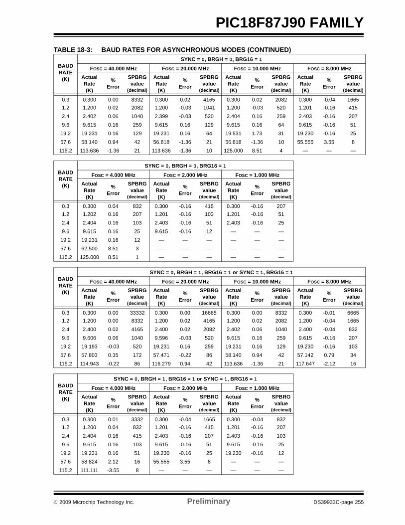
© 2009 Microchip Technology Inc. Preliminary DS39933C-page 255
PIC18F87J90 FAMILY
BAUDRATE
(K)
SYNC = 0, BRGH = 0, BRG16 = 1
FOSC = 40.000 MHz FOSC = 20.000 MHz FOSC = 10.000 MHz FOSC = 8.000 MHzActual Rate (K)
%Error
SPBRGvalue
(decimal)
Actual Rate (K)
%Error
SPBRGvalue
(decimal)
Actual Rate (K)
%Error
SPBRGvalue
(decimal)
Actual Rate (K)
%Error
SPBRGvalue
(decimal)
0.3 0.300 0.00 8332 0.300 0.02 4165 0.300 0.02 2082 0.300 -0.04 16651.2 1.200 0.02 2082 1.200 -0.03 1041 1.200 -0.03 520 1.201 -0.16 4152.4 2.402 0.06 1040 2.399 -0.03 520 2.404 0.16 259 2.403 -0.16 2079.6 9.615 0.16 259 9.615 0.16 129 9.615 0.16 64 9.615 -0.16 51
19.2 19.231 0.16 129 19.231 0.16 64 19.531 1.73 31 19.230 -0.16 2557.6 58.140 0.94 42 56.818 -1.36 21 56.818 -1.36 10 55.555 3.55 8115.2 113.636 -1.36 21 113.636 -1.36 10 125.000 8.51 4 — — —
BAUDRATE
(K)
SYNC = 0, BRGH = 0, BRG16 = 1
FOSC = 4.000 MHz FOSC = 2.000 MHz FOSC = 1.000 MHzActual Rate (K)
%Error
SPBRGvalue
(decimal)
Actual Rate (K)
%Error
SPBRGvalue
(decimal)
Actual Rate (K)
%Error
SPBRGvalue
(decimal)
0.3 0.300 0.04 832 0.300 -0.16 415 0.300 -0.16 2071.2 1.202 0.16 207 1.201 -0.16 103 1.201 -0.16 512.4 2.404 0.16 103 2.403 -0.16 51 2.403 -0.16 259.6 9.615 0.16 25 9.615 -0.16 12 — — —
19.2 19.231 0.16 12 — — — — — —57.6 62.500 8.51 3 — — — — — —115.2 125.000 8.51 1 — — — — — —
BAUDRATE
(K)
SYNC = 0, BRGH = 1, BRG16 = 1 or SYNC = 1, BRG16 = 1
FOSC = 40.000 MHz FOSC = 20.000 MHz FOSC = 10.000 MHz FOSC = 8.000 MHzActual Rate (K)
%Error
SPBRGvalue
(decimal)
Actual Rate (K)
%Error
SPBRGvalue
(decimal)
Actual Rate (K)
%Error
SPBRGvalue
(decimal)
Actual Rate (K)
%Error
SPBRGvalue
(decimal)
0.3 0.300 0.00 33332 0.300 0.00 16665 0.300 0.00 8332 0.300 -0.01 66651.2 1.200 0.00 8332 1.200 0.02 4165 1.200 0.02 2082 1.200 -0.04 16652.4 2.400 0.02 4165 2.400 0.02 2082 2.402 0.06 1040 2.400 -0.04 8329.6 9.606 0.06 1040 9.596 -0.03 520 9.615 0.16 259 9.615 -0.16 207
19.2 19.193 -0.03 520 19.231 0.16 259 19.231 0.16 129 19.230 -0.16 10357.6 57.803 0.35 172 57.471 -0.22 86 58.140 0.94 42 57.142 0.79 34115.2 114.943 -0.22 86 116.279 0.94 42 113.636 -1.36 21 117.647 -2.12 16
BAUDRATE
(K)
SYNC = 0, BRGH = 1, BRG16 = 1 or SYNC = 1, BRG16 = 1
FOSC = 4.000 MHz FOSC = 2.000 MHz FOSC = 1.000 MHzActual Rate (K)
%Error
SPBRGvalue
(decimal)
Actual Rate (K)
%Error
SPBRGvalue
(decimal)
Actual Rate (K)
%Error
SPBRGvalue
(decimal)
0.3 0.300 0.01 3332 0.300 -0.04 1665 0.300 -0.04 8321.2 1.200 0.04 832 1.201 -0.16 415 1.201 -0.16 2072.4 2.404 0.16 415 2.403 -0.16 207 2.403 -0.16 1039.6 9.615 0.16 103 9.615 -0.16 51 9.615 -0.16 25
19.2 19.231 0.16 51 19.230 -0.16 25 19.230 -0.16 1257.6 58.824 2.12 16 55.555 3.55 8 — — —115.2 111.111 -3.55 8 — — — — — —
TABLE 18-3: BAUD RATES FOR ASYNCHRONOUS MODES (CONTINUED)
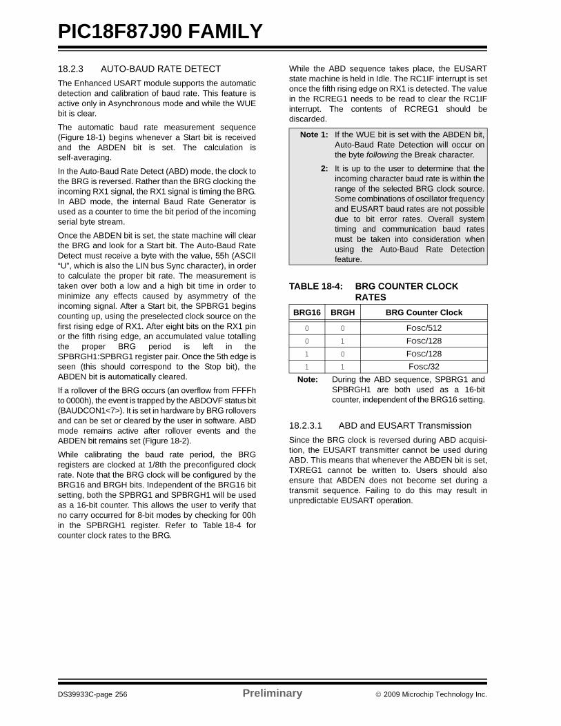
PIC18F87J90 FAMILY
DS39933C-page 256 Preliminary © 2009 Microchip Technology Inc.
18.2.3 AUTO-BAUD RATE DETECTThe Enhanced USART module supports the automaticdetection and calibration of baud rate. This feature isactive only in Asynchronous mode and while the WUEbit is clear.
The automatic baud rate measurement sequence(Figure 18-1) begins whenever a Start bit is receivedand the ABDEN bit is set. The calculation isself-averaging.
In the Auto-Baud Rate Detect (ABD) mode, the clock tothe BRG is reversed. Rather than the BRG clocking theincoming RX1 signal, the RX1 signal is timing the BRG.In ABD mode, the internal Baud Rate Generator isused as a counter to time the bit period of the incomingserial byte stream.
Once the ABDEN bit is set, the state machine will clearthe BRG and look for a Start bit. The Auto-Baud RateDetect must receive a byte with the value, 55h (ASCII“U”, which is also the LIN bus Sync character), in orderto calculate the proper bit rate. The measurement istaken over both a low and a high bit time in order tominimize any effects caused by asymmetry of theincoming signal. After a Start bit, the SPBRG1 beginscounting up, using the preselected clock source on thefirst rising edge of RX1. After eight bits on the RX1 pinor the fifth rising edge, an accumulated value totallingthe proper BRG period is left in theSPBRGH1:SPBRG1 register pair. Once the 5th edge isseen (this should correspond to the Stop bit), theABDEN bit is automatically cleared.
If a rollover of the BRG occurs (an overflow from FFFFhto 0000h), the event is trapped by the ABDOVF status bit(BAUDCON1<7>). It is set in hardware by BRG rolloversand can be set or cleared by the user in software. ABDmode remains active after rollover events and theABDEN bit remains set (Figure 18-2).
While calibrating the baud rate period, the BRGregisters are clocked at 1/8th the preconfigured clockrate. Note that the BRG clock will be configured by theBRG16 and BRGH bits. Independent of the BRG16 bitsetting, both the SPBRG1 and SPBRGH1 will be usedas a 16-bit counter. This allows the user to verify thatno carry occurred for 8-bit modes by checking for 00hin the SPBRGH1 register. Refer to Table 18-4 forcounter clock rates to the BRG.
While the ABD sequence takes place, the EUSARTstate machine is held in Idle. The RC1IF interrupt is setonce the fifth rising edge on RX1 is detected. The valuein the RCREG1 needs to be read to clear the RC1IFinterrupt. The contents of RCREG1 should bediscarded.
TABLE 18-4: BRG COUNTER CLOCK RATES
18.2.3.1 ABD and EUSART TransmissionSince the BRG clock is reversed during ABD acquisi-tion, the EUSART transmitter cannot be used duringABD. This means that whenever the ABDEN bit is set,TXREG1 cannot be written to. Users should alsoensure that ABDEN does not become set during atransmit sequence. Failing to do this may result inunpredictable EUSART operation.
Note 1: If the WUE bit is set with the ABDEN bit,Auto-Baud Rate Detection will occur onthe byte following the Break character.
2: It is up to the user to determine that theincoming character baud rate is within therange of the selected BRG clock source.Some combinations of oscillator frequencyand EUSART baud rates are not possibledue to bit error rates. Overall systemtiming and communication baud ratesmust be taken into consideration whenusing the Auto-Baud Rate Detectionfeature.
BRG16 BRGH BRG Counter Clock
0 0 FOSC/5120 1 FOSC/1281 0 FOSC/1281 1 FOSC/32
Note: During the ABD sequence, SPBRG1 andSPBRGH1 are both used as a 16-bitcounter, independent of the BRG16 setting.
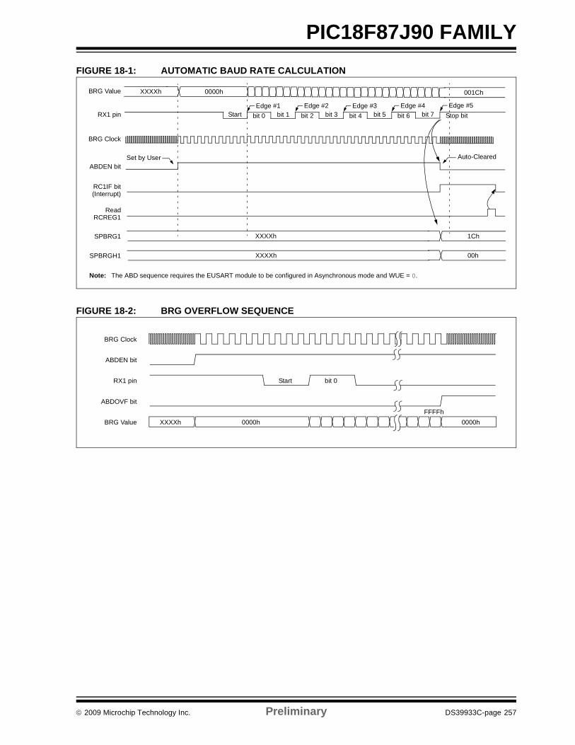
© 2009 Microchip Technology Inc. Preliminary DS39933C-page 257
PIC18F87J90 FAMILYFIGURE 18-1: AUTOMATIC BAUD RATE CALCULATION
FIGURE 18-2: BRG OVERFLOW SEQUENCE
BRG Value
RX1 pin
ABDEN bit
RC1IF bit
bit 0 bit 1
(Interrupt)
ReadRCREG1
BRG Clock
Start
Auto-ClearedSet by User
XXXXh 0000h
Edge #1bit 2 bit 3Edge #2
bit 4 bit 5Edge #3
bit 6 bit 7Edge #4
Stop bitEdge #5
001Ch
Note: The ABD sequence requires the EUSART module to be configured in Asynchronous mode and WUE = 0.
SPBRG1 XXXXh 1Ch
SPBRGH1 XXXXh 00h
Start bit 0
XXXXh 0000h 0000hFFFFh
BRG Clock
ABDEN bit
RX1 pin
ABDOVF bit
BRG Value
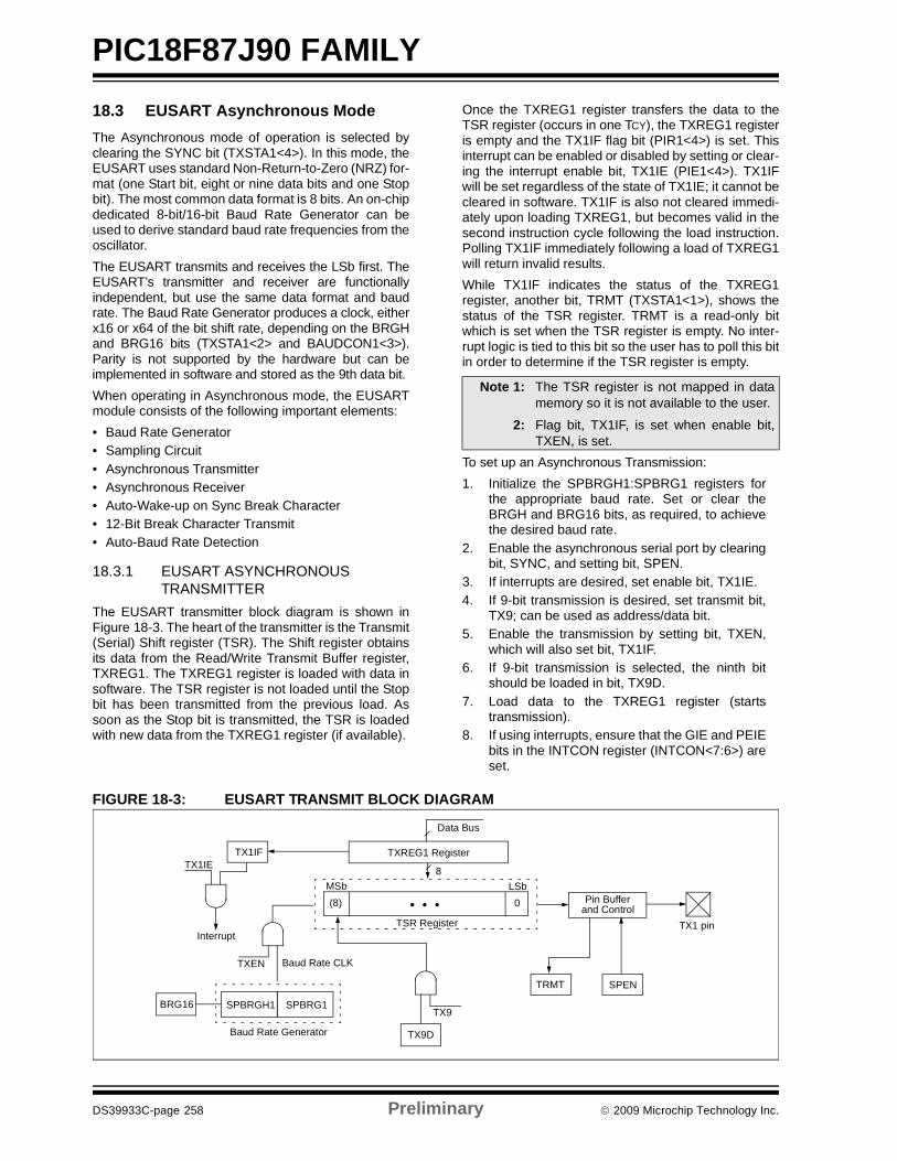
PIC18F87J90 FAMILY
DS39933C-page 258 Preliminary © 2009 Microchip Technology Inc.
18.3 EUSART Asynchronous ModeThe Asynchronous mode of operation is selected byclearing the SYNC bit (TXSTA1<4>). In this mode, theEUSART uses standard Non-Return-to-Zero (NRZ) for-mat (one Start bit, eight or nine data bits and one Stopbit). The most common data format is 8 bits. An on-chipdedicated 8-bit/16-bit Baud Rate Generator can beused to derive standard baud rate frequencies from theoscillator. The EUSART transmits and receives the LSb first. TheEUSART’s transmitter and receiver are functionallyindependent, but use the same data format and baudrate. The Baud Rate Generator produces a clock, eitherx16 or x64 of the bit shift rate, depending on the BRGHand BRG16 bits (TXSTA1<2> and BAUDCON1<3>).Parity is not supported by the hardware but can beimplemented in software and stored as the 9th data bit.When operating in Asynchronous mode, the EUSARTmodule consists of the following important elements:• Baud Rate Generator• Sampling Circuit• Asynchronous Transmitter• Asynchronous Receiver• Auto-Wake-up on Sync Break Character• 12-Bit Break Character Transmit• Auto-Baud Rate Detection
18.3.1 EUSART ASYNCHRONOUS TRANSMITTER
The EUSART transmitter block diagram is shown inFigure 18-3. The heart of the transmitter is the Transmit(Serial) Shift register (TSR). The Shift register obtainsits data from the Read/Write Transmit Buffer register,TXREG1. The TXREG1 register is loaded with data insoftware. The TSR register is not loaded until the Stopbit has been transmitted from the previous load. Assoon as the Stop bit is transmitted, the TSR is loadedwith new data from the TXREG1 register (if available).
Once the TXREG1 register transfers the data to theTSR register (occurs in one TCY), the TXREG1 registeris empty and the TX1IF flag bit (PIR1<4>) is set. Thisinterrupt can be enabled or disabled by setting or clear-ing the interrupt enable bit, TX1IE (PIE1<4>). TX1IFwill be set regardless of the state of TX1IE; it cannot becleared in software. TX1IF is also not cleared immedi-ately upon loading TXREG1, but becomes valid in thesecond instruction cycle following the load instruction.Polling TX1IF immediately following a load of TXREG1will return invalid results. While TX1IF indicates the status of the TXREG1register, another bit, TRMT (TXSTA1<1>), shows thestatus of the TSR register. TRMT is a read-only bitwhich is set when the TSR register is empty. No inter-rupt logic is tied to this bit so the user has to poll this bitin order to determine if the TSR register is empty.
To set up an Asynchronous Transmission:1. Initialize the SPBRGH1:SPBRG1 registers for
the appropriate baud rate. Set or clear theBRGH and BRG16 bits, as required, to achievethe desired baud rate.
2. Enable the asynchronous serial port by clearingbit, SYNC, and setting bit, SPEN.
3. If interrupts are desired, set enable bit, TX1IE.4. If 9-bit transmission is desired, set transmit bit,
TX9; can be used as address/data bit.5. Enable the transmission by setting bit, TXEN,
which will also set bit, TX1IF.6. If 9-bit transmission is selected, the ninth bit
should be loaded in bit, TX9D.7. Load data to the TXREG1 register (starts
transmission).8. If using interrupts, ensure that the GIE and PEIE
bits in the INTCON register (INTCON<7:6>) areset.
FIGURE 18-3: EUSART TRANSMIT BLOCK DIAGRAM
Note 1: The TSR register is not mapped in datamemory so it is not available to the user.
2: Flag bit, TX1IF, is set when enable bit,TXEN, is set.
TX1IFTX1IE
Interrupt
TXEN Baud Rate CLK
SPBRG1
Baud Rate Generator TX9D
MSb LSb
Data Bus
TXREG1 Register
TSR Register
(8) 0
TX9
TRMT SPEN
TX1 pin
Pin Bufferand Control
8
• • •
SPBRGH1BRG16
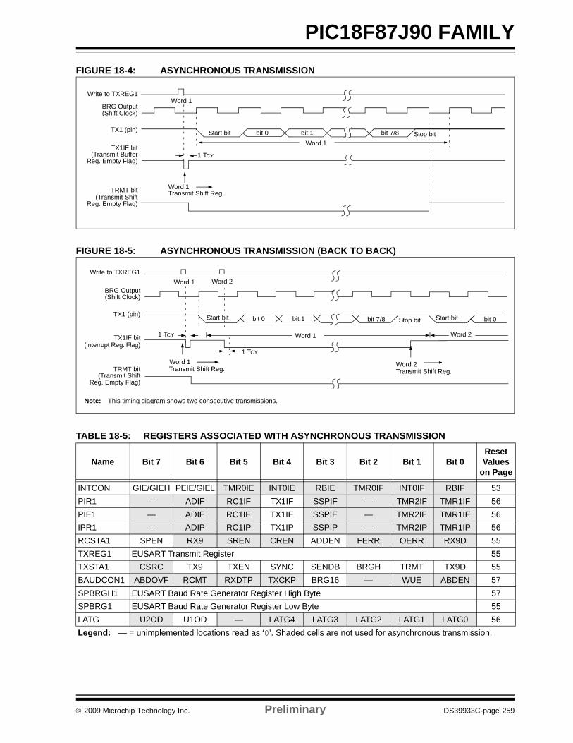
© 2009 Microchip Technology Inc. Preliminary DS39933C-page 259
PIC18F87J90 FAMILYFIGURE 18-4: ASYNCHRONOUS TRANSMISSION
FIGURE 18-5: ASYNCHRONOUS TRANSMISSION (BACK TO BACK)
TABLE 18-5: REGISTERS ASSOCIATED WITH ASYNCHRONOUS TRANSMISSION
Name Bit 7 Bit 6 Bit 5 Bit 4 Bit 3 Bit 2 Bit 1 Bit 0Reset Values
on Page
INTCON GIE/GIEH PEIE/GIEL TMR0IE INT0IE RBIE TMR0IF INT0IF RBIF 53PIR1 — ADIF RC1IF TX1IF SSPIF — TMR2IF TMR1IF 56PIE1 — ADIE RC1IE TX1IE SSPIE — TMR2IE TMR1IE 56IPR1 — ADIP RC1IP TX1IP SSPIP — TMR2IP TMR1IP 56RCSTA1 SPEN RX9 SREN CREN ADDEN FERR OERR RX9D 55TXREG1 EUSART Transmit Register 55TXSTA1 CSRC TX9 TXEN SYNC SENDB BRGH TRMT TX9D 55BAUDCON1 ABDOVF RCMT RXDTP TXCKP BRG16 — WUE ABDEN 57SPBRGH1 EUSART Baud Rate Generator Register High Byte 57SPBRG1 EUSART Baud Rate Generator Register Low Byte 55LATG U2OD U1OD — LATG4 LATG3 LATG2 LATG1 LATG0 56Legend: — = unimplemented locations read as ‘0’. Shaded cells are not used for asynchronous transmission.
Word 1
Word 1Transmit Shift Reg
Start bit bit 0 bit 1 bit 7/8
Write to TXREG1
BRG Output(Shift Clock)
TX1 (pin)
TX1IF bit(Transmit Buffer
Reg. Empty Flag)
TRMT bit(Transmit Shift
Reg. Empty Flag)
1 TCY
Word 1
Stop bit
Transmit Shift Reg.
Write to TXREG1
BRG Output(Shift Clock)
TX1 (pin)
TX1IF bit(Interrupt Reg. Flag)
TRMT bit(Transmit Shift
Reg. Empty Flag)
Word 1 Word 2
Word 1 Word 2
Stop bit Start bit
Transmit Shift Reg.
Word 1 Word 2
bit 0 bit 1 bit 7/8 bit 0
Note: This timing diagram shows two consecutive transmissions.
1 TCY
1 TCY
Start bit
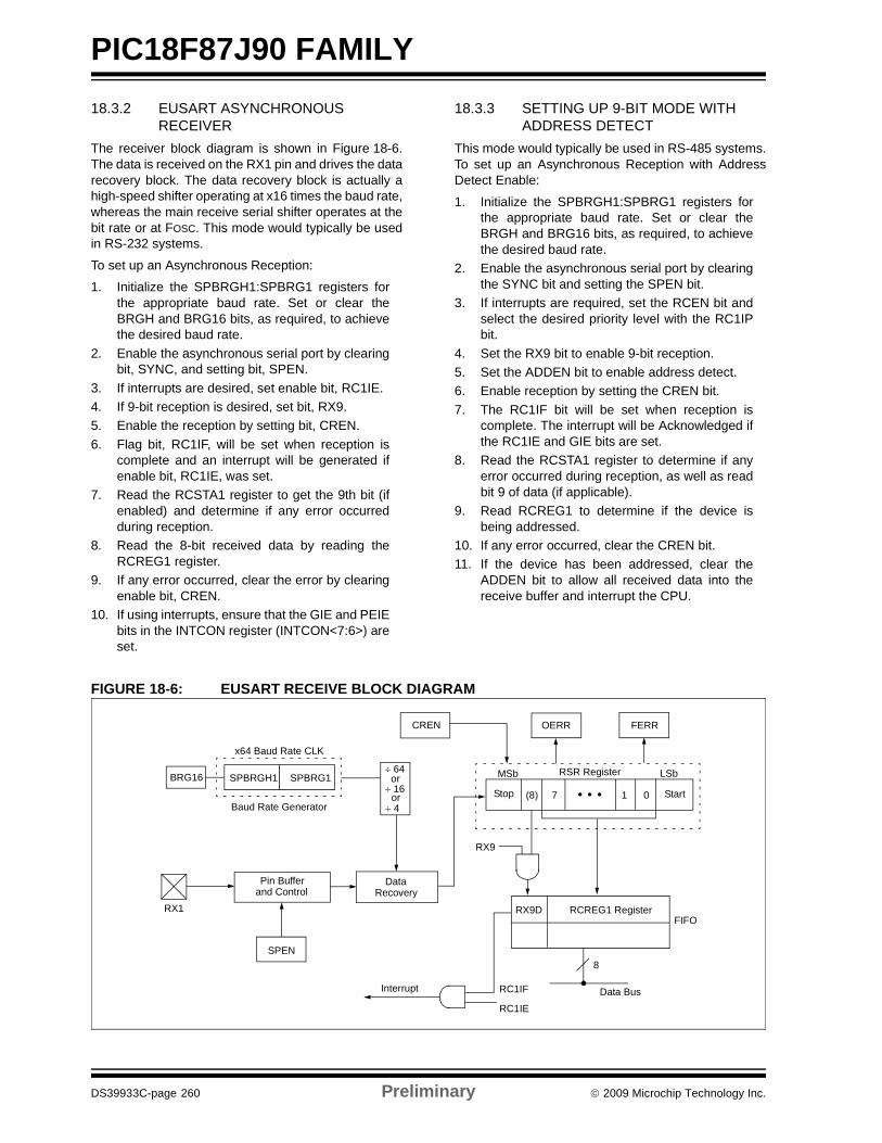
PIC18F87J90 FAMILY
DS39933C-page 260 Preliminary © 2009 Microchip Technology Inc.
18.3.2 EUSART ASYNCHRONOUS RECEIVER
The receiver block diagram is shown in Figure 18-6.The data is received on the RX1 pin and drives the datarecovery block. The data recovery block is actually ahigh-speed shifter operating at x16 times the baud rate,whereas the main receive serial shifter operates at thebit rate or at FOSC. This mode would typically be usedin RS-232 systems.
To set up an Asynchronous Reception:
1. Initialize the SPBRGH1:SPBRG1 registers forthe appropriate baud rate. Set or clear theBRGH and BRG16 bits, as required, to achievethe desired baud rate.
2. Enable the asynchronous serial port by clearingbit, SYNC, and setting bit, SPEN.
3. If interrupts are desired, set enable bit, RC1IE.4. If 9-bit reception is desired, set bit, RX9.5. Enable the reception by setting bit, CREN.6. Flag bit, RC1IF, will be set when reception is
complete and an interrupt will be generated ifenable bit, RC1IE, was set.
7. Read the RCSTA1 register to get the 9th bit (ifenabled) and determine if any error occurredduring reception.
8. Read the 8-bit received data by reading theRCREG1 register.
9. If any error occurred, clear the error by clearingenable bit, CREN.
10. If using interrupts, ensure that the GIE and PEIEbits in the INTCON register (INTCON<7:6>) areset.
18.3.3 SETTING UP 9-BIT MODE WITH ADDRESS DETECT
This mode would typically be used in RS-485 systems.To set up an Asynchronous Reception with AddressDetect Enable:
1. Initialize the SPBRGH1:SPBRG1 registers forthe appropriate baud rate. Set or clear theBRGH and BRG16 bits, as required, to achievethe desired baud rate.
2. Enable the asynchronous serial port by clearingthe SYNC bit and setting the SPEN bit.
3. If interrupts are required, set the RCEN bit andselect the desired priority level with the RC1IPbit.
4. Set the RX9 bit to enable 9-bit reception. 5. Set the ADDEN bit to enable address detect.6. Enable reception by setting the CREN bit.7. The RC1IF bit will be set when reception is
complete. The interrupt will be Acknowledged ifthe RC1IE and GIE bits are set.
8. Read the RCSTA1 register to determine if anyerror occurred during reception, as well as readbit 9 of data (if applicable).
9. Read RCREG1 to determine if the device isbeing addressed.
10. If any error occurred, clear the CREN bit. 11. If the device has been addressed, clear the
ADDEN bit to allow all received data into thereceive buffer and interrupt the CPU.
FIGURE 18-6: EUSART RECEIVE BLOCK DIAGRAM
x64 Baud Rate CLK
Baud Rate Generator
RX1
Pin Bufferand Control
SPEN
DataRecovery
CREN OERR FERR
RSR RegisterMSb LSb
RX9D RCREG1 RegisterFIFO
Interrupt RC1IF
RC1IEData Bus
8
÷ 64
÷ 16or
Stop Start(8) 7 1 0
RX9
• • •
SPBRG1SPBRGH1BRG16
or÷ 4
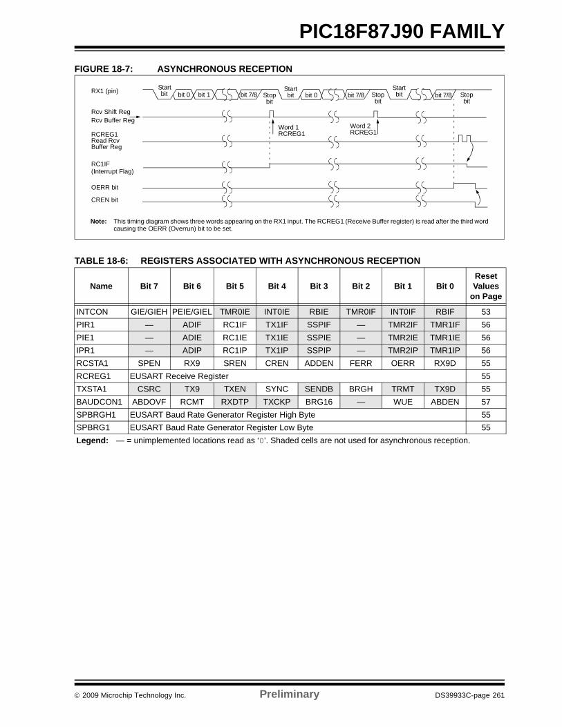
© 2009 Microchip Technology Inc. Preliminary DS39933C-page 261
PIC18F87J90 FAMILYFIGURE 18-7: ASYNCHRONOUS RECEPTION
TABLE 18-6: REGISTERS ASSOCIATED WITH ASYNCHRONOUS RECEPTION
Name Bit 7 Bit 6 Bit 5 Bit 4 Bit 3 Bit 2 Bit 1 Bit 0Reset Values
on Page
INTCON GIE/GIEH PEIE/GIEL TMR0IE INT0IE RBIE TMR0IF INT0IF RBIF 53PIR1 — ADIF RC1IF TX1IF SSPIF — TMR2IF TMR1IF 56PIE1 — ADIE RC1IE TX1IE SSPIE — TMR2IE TMR1IE 56IPR1 — ADIP RC1IP TX1IP SSPIP — TMR2IP TMR1IP 56RCSTA1 SPEN RX9 SREN CREN ADDEN FERR OERR RX9D 55RCREG1 EUSART Receive Register 55TXSTA1 CSRC TX9 TXEN SYNC SENDB BRGH TRMT TX9D 55BAUDCON1 ABDOVF RCMT RXDTP TXCKP BRG16 — WUE ABDEN 57SPBRGH1 EUSART Baud Rate Generator Register High Byte 55SPBRG1 EUSART Baud Rate Generator Register Low Byte 55Legend: — = unimplemented locations read as ‘0’. Shaded cells are not used for asynchronous reception.
Startbit bit 7/8bit 1bit 0 bit 7/8 bit 0Stop
bit
Startbit
Startbitbit 7/8 Stop
bitRX1 (pin)
Rcv Buffer RegRcv Shift Reg
Read RcvBuffer Reg
RCREG1
RC1IF(Interrupt Flag)
OERR bit
CREN bit
Word 1RCREG1
Word 2RCREG1
Stopbit
Note: This timing diagram shows three words appearing on the RX1 input. The RCREG1 (Receive Buffer register) is read after the third wordcausing the OERR (Overrun) bit to be set.
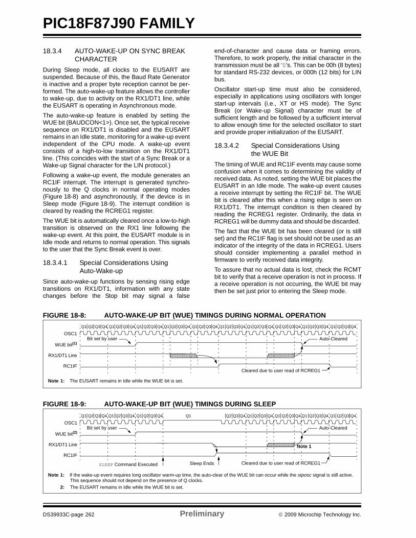
PIC18F87J90 FAMILY
DS39933C-page 262 Preliminary © 2009 Microchip Technology Inc.
18.3.4 AUTO-WAKE-UP ON SYNC BREAK CHARACTER
During Sleep mode, all clocks to the EUSART aresuspended. Because of this, the Baud Rate Generatoris inactive and a proper byte reception cannot be per-formed. The auto-wake-up feature allows the controllerto wake-up, due to activity on the RX1/DT1 line, whilethe EUSART is operating in Asynchronous mode.The auto-wake-up feature is enabled by setting theWUE bit (BAUDCON<1>). Once set, the typical receivesequence on RX1/DT1 is disabled and the EUSARTremains in an Idle state, monitoring for a wake-up eventindependent of the CPU mode. A wake-up eventconsists of a high-to-low transition on the RX1/DT1line. (This coincides with the start of a Sync Break or aWake-up Signal character for the LIN protocol.)Following a wake-up event, the module generates anRC1IF interrupt. The interrupt is generated synchro-nously to the Q clocks in normal operating modes(Figure 18-8) and asynchronously, if the device is inSleep mode (Figure 18-9). The interrupt condition iscleared by reading the RCREG1 register.The WUE bit is automatically cleared once a low-to-hightransition is observed on the RX1 line following thewake-up event. At this point, the EUSART module is inIdle mode and returns to normal operation. This signalsto the user that the Sync Break event is over.
18.3.4.1 Special Considerations Using Auto-Wake-up
Since auto-wake-up functions by sensing rising edgetransitions on RX1/DT1, information with any statechanges before the Stop bit may signal a false
end-of-character and cause data or framing errors.Therefore, to work properly, the initial character in thetransmission must be all ‘0’s. This can be 00h (8 bytes)for standard RS-232 devices, or 000h (12 bits) for LINbus.Oscillator start-up time must also be considered,especially in applications using oscillators with longerstart-up intervals (i.e., XT or HS mode). The SyncBreak (or Wake-up Signal) character must be ofsufficient length and be followed by a sufficient intervalto allow enough time for the selected oscillator to startand provide proper initialization of the EUSART.
18.3.4.2 Special Considerations Using the WUE Bit
The timing of WUE and RC1IF events may cause someconfusion when it comes to determining the validity ofreceived data. As noted, setting the WUE bit places theEUSART in an Idle mode. The wake-up event causesa receive interrupt by setting the RC1IF bit. The WUEbit is cleared after this when a rising edge is seen onRX1/DT1. The interrupt condition is then cleared byreading the RCREG1 register. Ordinarily, the data inRCREG1 will be dummy data and should be discarded. The fact that the WUE bit has been cleared (or is stillset) and the RC1IF flag is set should not be used as anindicator of the integrity of the data in RCREG1. Usersshould consider implementing a parallel method infirmware to verify received data integrity.To assure that no actual data is lost, check the RCMTbit to verify that a receive operation is not in process. Ifa receive operation is not occurring, the WUE bit maythen be set just prior to entering the Sleep mode.
FIGURE 18-8: AUTO-WAKE-UP BIT (WUE) TIMINGS DURING NORMAL OPERATION
FIGURE 18-9: AUTO-WAKE-UP BIT (WUE) TIMINGS DURING SLEEP
Q1 Q2 Q3 Q4 Q1 Q2 Q3 Q4 Q1 Q2 Q3 Q4 Q1 Q2 Q3 Q4 Q1 Q2 Q3 Q4 Q1 Q2 Q3 Q4 Q1 Q2 Q3 Q4 Q1 Q2 Q3 Q4 Q1 Q2 Q3 Q4 Q1 Q2 Q3 Q4
OSC1
WUE bit(1)
RX1/DT1 Line
RC1IFCleared due to user read of RCREG1
Note 1: The EUSART remains in Idle while the WUE bit is set.
Bit set by user Auto-Cleared
Q1 Q2 Q3 Q4 Q1 Q2 Q3 Q4 Q1 Q2 Q3 Q4 Q1 Q2 Q3 Q4 Q1 Q2 Q3 Q4 Q1 Q2 Q3 Q4 Q1 Q2 Q3 Q4 Q1 Q2 Q3 Q4
OSC1
WUE bit(2)
RX1/DT1 Line
RC1IF
Cleared due to user read of RCREG1SLEEP Command Executed
Note 1: If the wake-up event requires long oscillator warm-up time, the auto-clear of the WUE bit can occur while the stposc signal is still active.This sequence should not depend on the presence of Q clocks.
2: The EUSART remains in Idle while the WUE bit is set.
Sleep Ends
Auto-Cleared
Note 1
Bit set by user
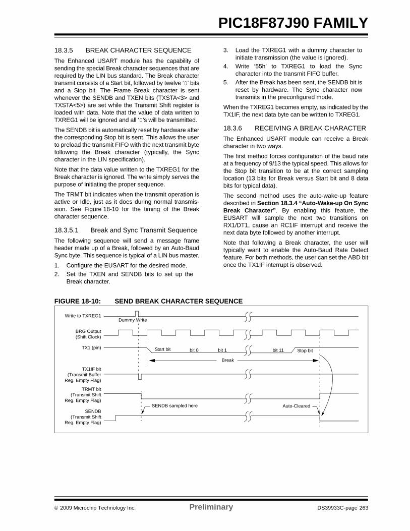
© 2009 Microchip Technology Inc. Preliminary DS39933C-page 263
PIC18F87J90 FAMILY18.3.5 BREAK CHARACTER SEQUENCEThe Enhanced USART module has the capability ofsending the special Break character sequences that arerequired by the LIN bus standard. The Break charactertransmit consists of a Start bit, followed by twelve ‘0’ bitsand a Stop bit. The Frame Break character is sentwhenever the SENDB and TXEN bits (TXSTA<3> andTXSTA<5>) are set while the Transmit Shift register isloaded with data. Note that the value of data written toTXREG1 will be ignored and all ‘0’s will be transmitted.
The SENDB bit is automatically reset by hardware afterthe corresponding Stop bit is sent. This allows the userto preload the transmit FIFO with the next transmit bytefollowing the Break character (typically, the Synccharacter in the LIN specification).
Note that the data value written to the TXREG1 for theBreak character is ignored. The write simply serves thepurpose of initiating the proper sequence.
The TRMT bit indicates when the transmit operation isactive or Idle, just as it does during normal transmis-sion. See Figure 18-10 for the timing of the Breakcharacter sequence.
18.3.5.1 Break and Sync Transmit SequenceThe following sequence will send a message frameheader made up of a Break, followed by an Auto-BaudSync byte. This sequence is typical of a LIN bus master.
1. Configure the EUSART for the desired mode.2. Set the TXEN and SENDB bits to set up the
Break character.
3. Load the TXREG1 with a dummy character toinitiate transmission (the value is ignored).
4. Write ‘55h’ to TXREG1 to load the Synccharacter into the transmit FIFO buffer.
5. After the Break has been sent, the SENDB bit isreset by hardware. The Sync character nowtransmits in the preconfigured mode.
When the TXREG1 becomes empty, as indicated by theTX1IF, the next data byte can be written to TXREG1.
18.3.6 RECEIVING A BREAK CHARACTERThe Enhanced USART module can receive a Breakcharacter in two ways.
The first method forces configuration of the baud rateat a frequency of 9/13 the typical speed. This allows forthe Stop bit transition to be at the correct samplinglocation (13 bits for Break versus Start bit and 8 databits for typical data).
The second method uses the auto-wake-up featuredescribed in Section 18.3.4 “Auto-Wake-up On SyncBreak Character”. By enabling this feature, theEUSART will sample the next two transitions onRX1/DT1, cause an RC1IF interrupt and receive thenext data byte followed by another interrupt.
Note that following a Break character, the user willtypically want to enable the Auto-Baud Rate Detectfeature. For both methods, the user can set the ABD bitonce the TX1IF interrupt is observed.
FIGURE 18-10: SEND BREAK CHARACTER SEQUENCE
Write to TXREG1
BRG Output(Shift Clock)
Start bit bit 0 bit 1 bit 11 Stop bit
Break
TX1IF bit(Transmit Buffer
Reg. Empty Flag)
TX1 (pin)
TRMT bit(Transmit Shift
Reg. Empty Flag)
SENDB(Transmit Shift
Reg. Empty Flag)
SENDB sampled here Auto-Cleared
Dummy Write
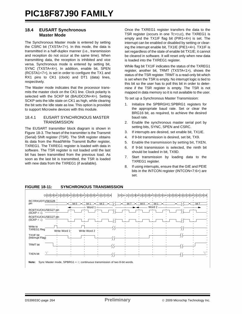
PIC18F87J90 FAMILY
DS39933C-page 264 Preliminary © 2009 Microchip Technology Inc.
18.4 EUSART Synchronous Master Mode
The Synchronous Master mode is entered by settingthe CSRC bit (TXSTA<7>). In this mode, the data istransmitted in a half-duplex manner (i.e., transmissionand reception do not occur at the same time). Whentransmitting data, the reception is inhibited and viceversa. Synchronous mode is entered by setting bit,SYNC (TXSTA<4>). In addition, enable bit, SPEN(RCSTA1<7>), is set in order to configure the TX1 andRX1 pins to CK1 (clock) and DT1 (data) lines,respectively.
The Master mode indicates that the processor trans-mits the master clock on the CK1 line. Clock polarity isselected with the SCKP bit (BAUDCON<4>). SettingSCKP sets the Idle state on CK1 as high, while clearingthe bit sets the Idle state as low. This option is providedto support Microwire devices with this module.
18.4.1 EUSART SYNCHRONOUS MASTER TRANSMISSION
The EUSART transmitter block diagram is shown inFigure 18-3. The heart of the transmitter is the Transmit(Serial) Shift register (TSR). The Shift register obtainsits data from the Read/Write Transmit Buffer register,TXREG1. The TXREG1 register is loaded with data insoftware. The TSR register is not loaded until the lastbit has been transmitted from the previous load. Assoon as the last bit is transmitted, the TSR is loadedwith new data from the TXREG1 (if available).
Once the TXREG1 register transfers the data to theTSR register (occurs in one TCYCLE), the TXREG1 isempty and the TX1IF flag bit (PIR1<4>) is set. Theinterrupt can be enabled or disabled by setting or clear-ing the interrupt enable bit, TX1IE (PIE1<4>). TX1IF isset regardless of the state of enable bit TX1IE; it cannotbe cleared in software. It will reset only when new datais loaded into the TXREG1 register.
While flag bit TX1IF indicates the status of the TXREG1register, another bit, TRMT (TXSTA<1>), shows thestatus of the TSR register. TRMT is a read-only bit whichis set when the TSR is empty. No interrupt logic is tied tothis bit so the user has to poll this bit in order to deter-mine if the TSR register is empty. The TSR is notmapped in data memory so it is not available to the user.
To set up a Synchronous Master Transmission:
1. Initialize the SPBRGH1:SPBRG1 registers forthe appropriate baud rate. Set or clear theBRG16 bit, as required, to achieve the desiredbaud rate.
2. Enable the synchronous master serial port bysetting bits, SYNC, SPEN and CSRC.
3. If interrupts are desired, set enable bit, TX1IE.4. If 9-bit transmission is desired, set bit, TX9.5. Enable the transmission by setting bit, TXEN.6. If 9-bit transmission is selected, the ninth bit
should be loaded in bit, TX9D.7. Start transmission by loading data to the
TXREG1 register.8. If using interrupts, ensure that the GIE and PEIE
bits in the INTCON register (INTCON<7:6>) areset.
FIGURE 18-11: SYNCHRONOUS TRANSMISSION
bit 0 bit 1 bit 7Word 1
Q1 Q2 Q3 Q4 Q1Q2 Q3 Q4 Q1Q2 Q3 Q4 Q1Q2 Q3 Q4 Q1Q2 Q3 Q4 Q3 Q4 Q1 Q2 Q3Q4 Q1Q2 Q3Q4 Q1Q2 Q3 Q4 Q1Q2Q3 Q4 Q1Q2 Q3 Q4 Q1Q2 Q3 Q4
bit 2 bit 0 bit 1 bit 7RC7/RX1/DT1/SEG28
Write toTXREG1 Reg
TX1IF bit(Interrupt Flag)
TXEN bit ‘1’ ‘1’
Word 2
TRMT bit
Write Word 1 Write Word 2
Note: Sync Master mode, SPBRG1 = 0; continuous transmission of two 8-bit words.
pin
RC6/TX1/CK1/SEG27 pin(SCKP = 0)
(SCKP = 1)
RC6/TX1/CK1/SEG27 pin
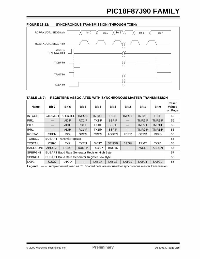
© 2009 Microchip Technology Inc. Preliminary DS39933C-page 265
PIC18F87J90 FAMILYFIGURE 18-12: SYNCHRONOUS TRANSMISSION (THROUGH TXEN)
TABLE 18-7: REGISTERS ASSOCIATED WITH SYNCHRONOUS MASTER TRANSMISSION
Name Bit 7 Bit 6 Bit 5 Bit 4 Bit 3 Bit 2 Bit 1 Bit 0Reset Values
on Page
INTCON GIE/GIEH PEIE/GIEL TMR0IE INT0IE RBIE TMR0IF INT0IF RBIF 53PIR1 — ADIF RC1IF TX1IF SSPIF — TMR2IF TMR1IF 56PIE1 — ADIE RC1IE TX1IE SSPIE — TMR2IE TMR1IE 56IPR1 — ADIP RC1IP TX1IP SSPIP — TMR2IP TMR1IP 56RCSTA1 SPEN RX9 SREN CREN ADDEN FERR OERR RX9D 55TXREG1 EUSART Transmit Register 55TXSTA1 CSRC TX9 TXEN SYNC SENDB BRGH TRMT TX9D 55BAUDCON1 ABDOVF RCMT RXDTP TXCKP BRG16 — WUE ABDEN 57SPBRGH1 EUSART Baud Rate Generator Register High Byte 57SPBRG1 EUSART Baud Rate Generator Register Low Byte 55LATG U2OD U1OD — LATG4 LATG3 LATG2 LATG1 LATG0 56Legend: — = unimplemented, read as ‘0’. Shaded cells are not used for synchronous master transmission.
RC7/RX1/DT1/SEG28 pin
RC6/TX1/CK1/SEG27 pin
Write toTXREG1 Reg
TX1IF bit
TRMT bit
bit 0 bit 1 bit 2 bit 6 bit 7
TXEN bit
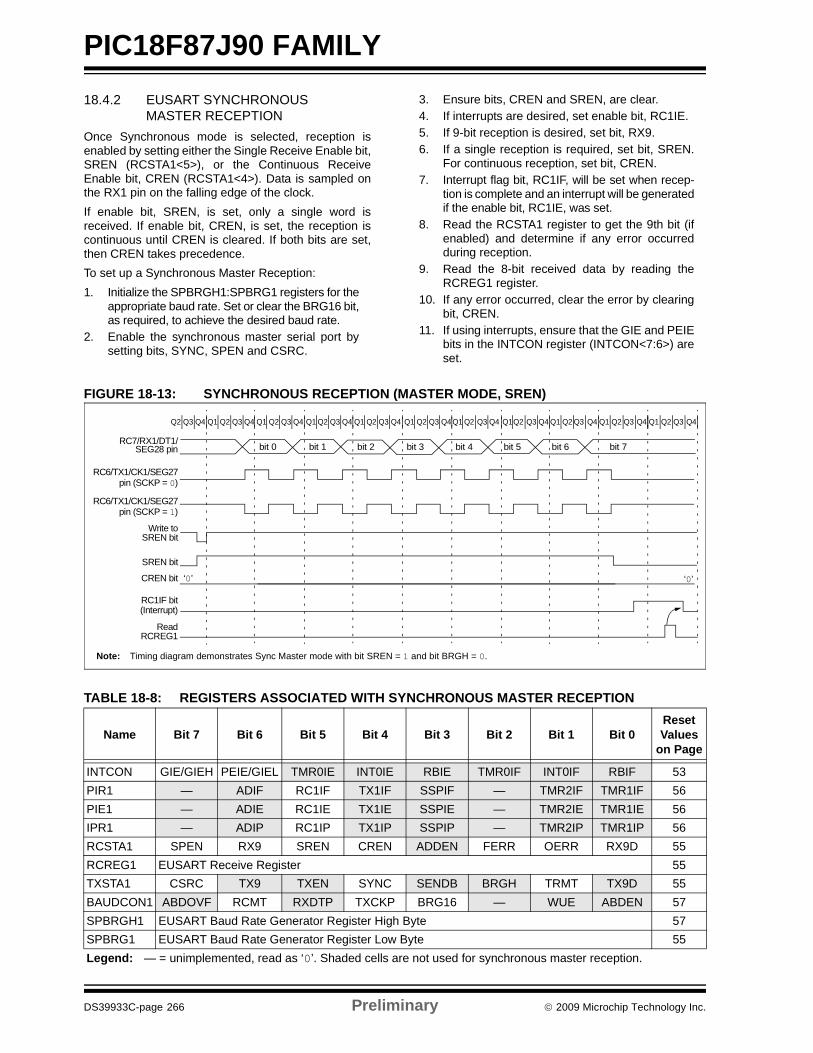
PIC18F87J90 FAMILY
DS39933C-page 266 Preliminary © 2009 Microchip Technology Inc.
18.4.2 EUSART SYNCHRONOUS MASTER RECEPTION
Once Synchronous mode is selected, reception isenabled by setting either the Single Receive Enable bit,SREN (RCSTA1<5>), or the Continuous ReceiveEnable bit, CREN (RCSTA1<4>). Data is sampled onthe RX1 pin on the falling edge of the clock.If enable bit, SREN, is set, only a single word isreceived. If enable bit, CREN, is set, the reception iscontinuous until CREN is cleared. If both bits are set,then CREN takes precedence.To set up a Synchronous Master Reception:1. Initialize the SPBRGH1:SPBRG1 registers for the
appropriate baud rate. Set or clear the BRG16 bit,as required, to achieve the desired baud rate.
2. Enable the synchronous master serial port bysetting bits, SYNC, SPEN and CSRC.
3. Ensure bits, CREN and SREN, are clear.4. If interrupts are desired, set enable bit, RC1IE.5. If 9-bit reception is desired, set bit, RX9.6. If a single reception is required, set bit, SREN.
For continuous reception, set bit, CREN.7. Interrupt flag bit, RC1IF, will be set when recep-
tion is complete and an interrupt will be generatedif the enable bit, RC1IE, was set.
8. Read the RCSTA1 register to get the 9th bit (ifenabled) and determine if any error occurredduring reception.
9. Read the 8-bit received data by reading theRCREG1 register.
10. If any error occurred, clear the error by clearingbit, CREN.
11. If using interrupts, ensure that the GIE and PEIEbits in the INTCON register (INTCON<7:6>) areset.
FIGURE 18-13: SYNCHRONOUS RECEPTION (MASTER MODE, SREN)
TABLE 18-8: REGISTERS ASSOCIATED WITH SYNCHRONOUS MASTER RECEPTION
Name Bit 7 Bit 6 Bit 5 Bit 4 Bit 3 Bit 2 Bit 1 Bit 0Reset Values
on Page
INTCON GIE/GIEH PEIE/GIEL TMR0IE INT0IE RBIE TMR0IF INT0IF RBIF 53PIR1 — ADIF RC1IF TX1IF SSPIF — TMR2IF TMR1IF 56PIE1 — ADIE RC1IE TX1IE SSPIE — TMR2IE TMR1IE 56IPR1 — ADIP RC1IP TX1IP SSPIP — TMR2IP TMR1IP 56RCSTA1 SPEN RX9 SREN CREN ADDEN FERR OERR RX9D 55RCREG1 EUSART Receive Register 55TXSTA1 CSRC TX9 TXEN SYNC SENDB BRGH TRMT TX9D 55BAUDCON1 ABDOVF RCMT RXDTP TXCKP BRG16 — WUE ABDEN 57SPBRGH1 EUSART Baud Rate Generator Register High Byte 57SPBRG1 EUSART Baud Rate Generator Register Low Byte 55Legend: — = unimplemented, read as ‘0’. Shaded cells are not used for synchronous master reception.
CREN bit
RC7/RX1/DT1/
RC6/TX1/CK1/SEG27
Write toSREN bit
SREN bit
RC1IF bit(Interrupt)
ReadRCREG1
Q3 Q4 Q1 Q2 Q3 Q4 Q1 Q2 Q3 Q4Q2 Q1 Q2 Q3 Q4 Q1 Q2 Q3 Q4 Q1 Q2 Q3 Q4 Q1 Q2 Q3 Q4 Q1Q2 Q3 Q4 Q1 Q2 Q3 Q4 Q1 Q2 Q3 Q4
‘0’
bit 0 bit 1 bit 2 bit 3 bit 4 bit 5 bit 6 bit 7
‘0’
Q1 Q2 Q3 Q4
Note: Timing diagram demonstrates Sync Master mode with bit SREN = 1 and bit BRGH = 0.
RC6/TX1/CK1/SEG27
SEG28 pin
pin (SCKP = 0)
pin (SCKP = 1)
© 2009 Microchip Technology Inc. Preliminary DS39933C-page 267
PIC18F87J90 FAMILY18.5 EUSART Synchronous Slave ModeSynchronous Slave mode is entered by clearing bitCSRC (TXSTA<7>). This mode differs from theSynchronous Master mode in that the shift clock issupplied externally at the CK1 pin (instead of beingsupplied internally in Master mode). This allows thedevice to transfer or receive data while in anylow-power mode.
18.5.1 EUSART SYNCHRONOUS SLAVE TRANSMIT
The operation of the Synchronous Master and Slavemodes are identical except in the case of the Sleepmode.
If two words are written to the TXREG1 and then theSLEEP instruction is executed, the following will occur:
a) The first word will immediately transfer to theTSR register and transmit.
b) The second word will remain in the TXREG1register.
c) Flag bit, TX1IF, will not be set. d) When the first word has been shifted out of TSR,
the TXREG1 register will transfer the secondword to the TSR and flag bit, TX1IF, will now beset.
e) If enable bit, TX1IE, is set, the interrupt will wakethe chip from Sleep. If the global interrupt isenabled, the program will branch to the interruptvector.
To set up a Synchronous Slave Transmission:
1. Enable the synchronous slave serial port bysetting bits, SYNC and SPEN, and clearing bit,CSRC.
2. Clear bits, CREN and SREN.3. If interrupts are desired, set enable bit, TX1IE.4. If 9-bit transmission is desired, set bit, TX9.5. Enable the transmission by setting enable bit,
TXEN.6. If 9-bit transmission is selected, the ninth bit
should be loaded in bit, TX9D.7. Start transmission by loading data to the
TXREG1 register.8. If using interrupts, ensure that the GIE and PEIE
bits in the INTCON register (INTCON<7:6>) areset.
TABLE 18-9: REGISTERS ASSOCIATED WITH SYNCHRONOUS SLAVE TRANSMISSION
Name Bit 7 Bit 6 Bit 5 Bit 4 Bit 3 Bit 2 Bit 1 Bit 0Reset Values
on Page
INTCON GIE/GIEH PEIE/GIEL TMR0IE INT0IE RBIE TMR0IF INT0IF RBIF 53PIR1 — ADIF RC1IF TX1IF SSPIF — TMR2IF TMR1IF 56PIE1 — ADIE RC1IE TX1IE SSPIE — TMR2IE TMR1IE 56IPR1 — ADIP RC1IP TX1IP SSPIP — TMR2IP TMR1IP 56RCSTA1 SPEN RX9 SREN CREN ADDEN FERR OERR RX9D 55TXREG1 EUSART Transmit Register 55TXSTA1 CSRC TX9 TXEN SYNC SENDB BRGH TRMT TX9D 55BAUDCON1 ABDOVF RCMT RXDTP TXCKP BRG16 — WUE ABDEN 57SPBRGH1 EUSART Baud Rate Generator Register High Byte 57SPBRG1 EUSART Baud Rate Generator Register Low Byte 55LATG U2OD U1OD — LATG4 LATG3 LATG2 LATG1 LATG0 56Legend: — = unimplemented, read as ‘0’. Shaded cells are not used for synchronous slave transmission.
PIC18F87J90 FAMILY
DS39933C-page 268 Preliminary © 2009 Microchip Technology Inc.
18.5.2 EUSART SYNCHRONOUS SLAVE RECEPTION
The operation of the Synchronous Master and Slavemodes is identical except in the case of Sleep or anyIdle mode, and bit SREN, which is a “don’t care” inSlave mode.
If receive is enabled by setting the CREN bit prior toentering Sleep or any Idle mode, then a word may bereceived while in this low-power mode. Once the wordis received, the RSR register will transfer the data to theRCREG1 register; if the RC1IE enable bit is set, theinterrupt generated will wake the chip from thelow-power mode. If the global interrupt is enabled, theprogram will branch to the interrupt vector.
To set up a Synchronous Slave Reception:
1. Enable the synchronous master serial port bysetting bits, SYNC and SPEN, and clearing bit,CSRC.
2. If interrupts are desired, set enable bit, RC1IE.3. If 9-bit reception is desired, set bit, RX9.4. To enable reception, set enable bit, CREN.5. Flag bit, RC1IF, will be set when reception is
complete. An interrupt will be generated ifenable bit, RC1IE, was set.
6. Read the RCSTA1 register to get the 9th bit (ifenabled) and determine if any error occurredduring reception.
7. Read the 8-bit received data by reading theRCREG1 register.
8. If any error occurred, clear the error by clearingbit, CREN.
9. If using interrupts, ensure that the GIE and PEIEbits in the INTCON register (INTCON<7:6>) areset.
TABLE 18-10: REGISTERS ASSOCIATED WITH SYNCHRONOUS SLAVE RECEPTION
Name Bit 7 Bit 6 Bit 5 Bit 4 Bit 3 Bit 2 Bit 1 Bit 0Reset Values
on Page
INTCON GIE/GIEH PEIE/GIEL TMR0IE INT0IE RBIE TMR0IF INT0IF RBIF 53PIR1 — ADIF RC1IF TX1IF SSPIF — TMR2IF TMR1IF 56PIE1 — ADIE RC1IE TX1IE SSPIE — TMR2IE TMR1IE 56IPR1 — ADIP RC1IP TX1IP SSPIP — TMR2IP TMR1IP 56RCSTA1 SPEN RX9 SREN CREN ADDEN FERR OERR RX9D 55RCREG1 EUSART Receive Register 55TXSTA1 CSRC TX9 TXEN SYNC SENDB BRGH TRMT TX9D 55BAUDCON1 ABDOVF RCMT RXDTP TXCKP BRG16 — WUE ABDEN 57SPBRGH1 EUSART Baud Rate Generator Register High Byte 57SPBRG1 EUSART Baud Rate Generator Register Low Byte 55Legend: — = unimplemented, read as ‘0’. Shaded cells are not used for synchronous slave reception.
© 2009 Microchip Technology Inc. Preliminary DS39933C-page 269
PIC18F87J90 FAMILY
19.0 ADDRESSABLE UNIVERSAL SYNCHRONOUS ASYNCHRONOUS RECEIVER TRANSMITTER (AUSART)
The Addressable Universal Synchronous Asynchro-nous Receiver Transmitter (AUSART) module is verysimilar in function to the Enhanced USART module,discussed in the previous chapter. It is provided as anadditional channel for serial communication withexternal devices, for those situations that do not requireauto-baud detection or LIN bus support.
The AUSART can be configured in the following modes:
• Asynchronous (full-duplex)• Synchronous – Master (half-duplex)• Synchronous – Slave (half-duplex)
The pins of the AUSART module are multiplexed withthe functions of PORTG (RG1/TX2/CK2 andRG2/RX2/DT2/VLCAP1, respectively). In order toconfigure these pins as an AUSART:
• bit SPEN (RCSTA2<7>) must be set (= 1)• bit TRISG<2> must be set (= 1)• bit TRISG<1> must be cleared (= 0) for
Asynchronous and Synchronous Master modes• bit TRISG<1> must be set (= 1) for Synchronous
Slave mode
The driver for the TX2 output pin can also be optionallyconfigured as an open-drain output. This feature allowsthe voltage level on the pin to be pulled to a higher levelthrough an external pull-up resistor, and allows theoutput to communicate with external circuits without theneed for additional level shifters.
The open-drain output option is controlled by the U2ODbit (LATG<7>). Setting the bit configures the pin foropen-drain operation.
19.1 Control RegistersThe operation of the Addressable USART module iscontrolled through two registers, TXSTA2 andRXSTA2. These are detailed in Register 19-1 andRegister 19-2, respectively.
Note: The AUSART control will automaticallyreconfigure the pin from input to output asneeded.
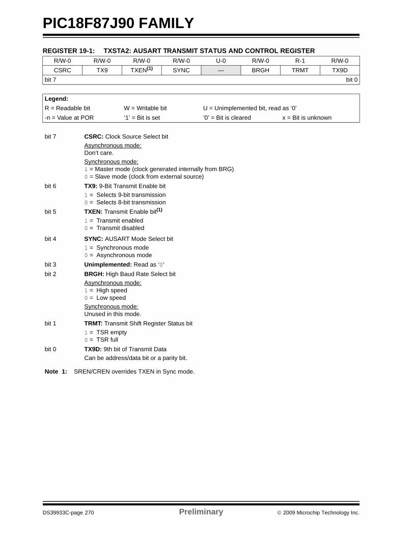
PIC18F87J90 FAMILY
DS39933C-page 270 Preliminary © 2009 Microchip Technology Inc.
REGISTER 19-1: TXSTA2: AUSART TRANSMIT STATUS AND CONTROL REGISTERR/W-0 R/W-0 R/W-0 R/W-0 U-0 R/W-0 R-1 R/W-0CSRC TX9 TXEN(1) SYNC — BRGH TRMT TX9D
bit 7 bit 0
Legend:R = Readable bit W = Writable bit U = Unimplemented bit, read as ‘0’-n = Value at POR ‘1’ = Bit is set ‘0’ = Bit is cleared x = Bit is unknown
bit 7 CSRC: Clock Source Select bitAsynchronous mode: Don’t care.Synchronous mode: 1 = Master mode (clock generated internally from BRG)0 = Slave mode (clock from external source)
bit 6 TX9: 9-Bit Transmit Enable bit 1 = Selects 9-bit transmission 0 = Selects 8-bit transmission
bit 5 TXEN: Transmit Enable bit(1) 1 = Transmit enabled0 = Transmit disabled
bit 4 SYNC: AUSART Mode Select bit 1 = Synchronous mode 0 = Asynchronous mode
bit 3 Unimplemented: Read as ‘0’ bit 2 BRGH: High Baud Rate Select bit
Asynchronous mode: 1 = High speed 0 = Low speedSynchronous mode: Unused in this mode.
bit 1 TRMT: Transmit Shift Register Status bit1 = TSR empty 0 = TSR full
bit 0 TX9D: 9th bit of Transmit DataCan be address/data bit or a parity bit.
Note 1: SREN/CREN overrides TXEN in Sync mode.

© 2009 Microchip Technology Inc. Preliminary DS39933C-page 271
PIC18F87J90 FAMILYREGISTER 19-2: RCSTA2: AUSART RECEIVE STATUS AND CONTROL REGISTER
R/W-0 R/W-0 R/W-0 R/W-0 R/W-0 R-0 R-0 R-xSPEN RX9 SREN CREN ADDEN FERR OERR RX9D
bit 7 bit 0
Legend:R = Readable bit W = Writable bit U = Unimplemented bit, read as ‘0’-n = Value at POR ‘1’ = Bit is set ‘0’ = Bit is cleared x = Bit is unknown
bit 7 SPEN: Serial Port Enable bit1 = Serial port enabled (configures RX2/DT2 and TX2/CK2 pins as serial port pins)0 = Serial port disabled (held in Reset)
bit 6 RX9: 9-Bit Receive Enable bit1 = Selects 9-bit reception 0 = Selects 8-bit reception
bit 5 SREN: Single Receive Enable bit Asynchronous mode: Don’t care.Synchronous mode – Master: 1 = Enables single receive0 = Disables single receive This bit is cleared after reception is complete.Synchronous mode – Slave: Don’t care.
bit 4 CREN: Continuous Receive Enable bit Asynchronous mode: 1 = Enables receiver0 = Disables receiverSynchronous mode: 1 = Enables continuous receive until enable bit, CREN, is cleared (CREN overrides SREN) 0 = Disables continuous receive
bit 3 ADDEN: Address Detect Enable bitAsynchronous mode 9-bit (RX9 = 1):1 = Enables address detection, enables interrupt and loads the receive buffer when RSR<8> is set0 = Disables address detection, all bytes are received and ninth bit can be used as parity bitAsynchronous mode 9-bit (RX9 = 0):Don’t care.
bit 2 FERR: Framing Error bit 1 = Framing error (can be updated by reading RCREG2 register and receiving next valid byte)0 = No framing error
bit 1 OERR: Overrun Error bit 1 = Overrun error (can be cleared by clearing bit CREN) 0 = No overrun error
bit 0 RX9D: 9th bit of Received Data This can be address/data bit or a parity bit and must be calculated by user firmware.
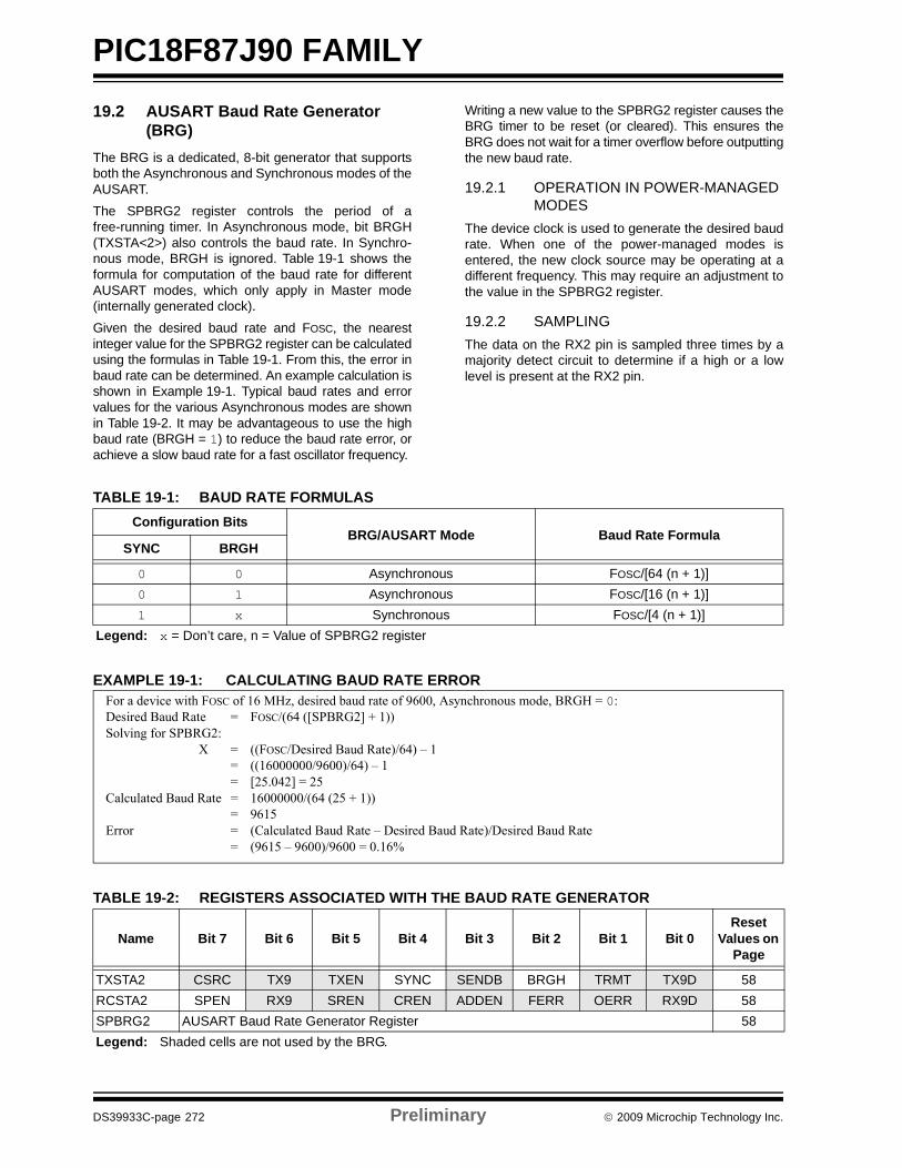
PIC18F87J90 FAMILY
DS39933C-page 272 Preliminary © 2009 Microchip Technology Inc.
19.2 AUSART Baud Rate Generator (BRG)
The BRG is a dedicated, 8-bit generator that supportsboth the Asynchronous and Synchronous modes of theAUSART.The SPBRG2 register controls the period of afree-running timer. In Asynchronous mode, bit BRGH(TXSTA<2>) also controls the baud rate. In Synchro-nous mode, BRGH is ignored. Table 19-1 shows theformula for computation of the baud rate for differentAUSART modes, which only apply in Master mode(internally generated clock).Given the desired baud rate and FOSC, the nearestinteger value for the SPBRG2 register can be calculatedusing the formulas in Table 19-1. From this, the error inbaud rate can be determined. An example calculation isshown in Example 19-1. Typical baud rates and errorvalues for the various Asynchronous modes are shownin Table 19-2. It may be advantageous to use the highbaud rate (BRGH = 1) to reduce the baud rate error, orachieve a slow baud rate for a fast oscillator frequency.
Writing a new value to the SPBRG2 register causes theBRG timer to be reset (or cleared). This ensures theBRG does not wait for a timer overflow before outputtingthe new baud rate.
19.2.1 OPERATION IN POWER-MANAGED MODES
The device clock is used to generate the desired baudrate. When one of the power-managed modes isentered, the new clock source may be operating at adifferent frequency. This may require an adjustment tothe value in the SPBRG2 register.
19.2.2 SAMPLINGThe data on the RX2 pin is sampled three times by amajority detect circuit to determine if a high or a lowlevel is present at the RX2 pin.
TABLE 19-1: BAUD RATE FORMULAS
EXAMPLE 19-1: CALCULATING BAUD RATE ERROR
TABLE 19-2: REGISTERS ASSOCIATED WITH THE BAUD RATE GENERATOR
Configuration BitsBRG/AUSART Mode Baud Rate Formula
SYNC BRGH
0 0 Asynchronous FOSC/[64 (n + 1)]0 1 Asynchronous FOSC/[16 (n + 1)]1 x Synchronous FOSC/[4 (n + 1)]
Legend: x = Don’t care, n = Value of SPBRG2 register
Name Bit 7 Bit 6 Bit 5 Bit 4 Bit 3 Bit 2 Bit 1 Bit 0Reset
Values on Page
TXSTA2 CSRC TX9 TXEN SYNC SENDB BRGH TRMT TX9D 58RCSTA2 SPEN RX9 SREN CREN ADDEN FERR OERR RX9D 58SPBRG2 AUSART Baud Rate Generator Register 58Legend: Shaded cells are not used by the BRG.
For a device with FOSC of 16 MHz, desired baud rate of 9600, Asynchronous mode, BRGH = 0:Desired Baud Rate = FOSC/(64 ([SPBRG2] + 1)) Solving for SPBRG2:
X = ((FOSC/Desired Baud Rate)/64) – 1= ((16000000/9600)/64) – 1 = [25.042] = 25
Calculated Baud Rate = 16000000/(64 (25 + 1)) = 9615
Error = (Calculated Baud Rate – Desired Baud Rate)/Desired Baud Rate= (9615 – 9600)/9600 = 0.16%
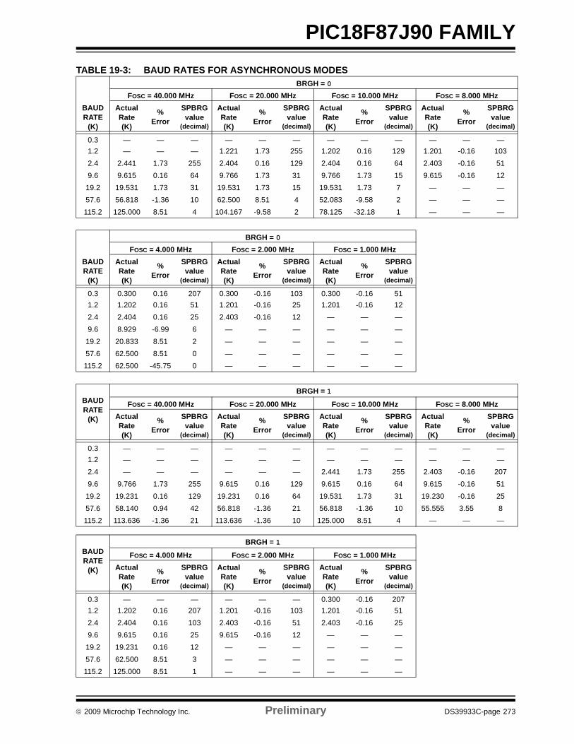
© 2009 Microchip Technology Inc. Preliminary DS39933C-page 273
PIC18F87J90 FAMILYTABLE 19-3: BAUD RATES FOR ASYNCHRONOUS MODES
BRGH = 0FOSC = 40.000 MHz FOSC = 20.000 MHz FOSC = 10.000 MHz FOSC = 8.000 MHz
BAUDRATE
(K)
Actual Rate (K)
%Error
SPBRGvalue
(decimal)
Actual Rate (K)
%Error
SPBRGvalue
(decimal)
Actual Rate (K)
%Error
SPBRGvalue
(decimal)
Actual Rate (K)
%Error
SPBRGvalue
(decimal)
0.3 — — — — — — — — — — — —1.2 — — — 1.221 1.73 255 1.202 0.16 129 1.201 -0.16 1032.4 2.441 1.73 255 2.404 0.16 129 2.404 0.16 64 2.403 -0.16 519.6 9.615 0.16 64 9.766 1.73 31 9.766 1.73 15 9.615 -0.16 12
19.2 19.531 1.73 31 19.531 1.73 15 19.531 1.73 7 — — —57.6 56.818 -1.36 10 62.500 8.51 4 52.083 -9.58 2 — — —115.2 125.000 8.51 4 104.167 -9.58 2 78.125 -32.18 1 — — —
BRGH = 0FOSC = 4.000 MHz FOSC = 2.000 MHz FOSC = 1.000 MHz
BAUDRATE
(K)
Actual Rate (K)
%Error
SPBRGvalue
(decimal)
Actual Rate (K)
%Error
SPBRGvalue
(decimal)
Actual Rate (K)
%Error
SPBRGvalue
(decimal)
0.3 0.300 0.16 207 0.300 -0.16 103 0.300 -0.16 511.2 1.202 0.16 51 1.201 -0.16 25 1.201 -0.16 122.4 2.404 0.16 25 2.403 -0.16 12 — — —9.6 8.929 -6.99 6 — — — — — —
19.2 20.833 8.51 2 — — — — — —57.6 62.500 8.51 0 — — — — — —115.2 62.500 -45.75 0 — — — — — —
BAUDRATE
(K)
BRGH = 1
FOSC = 40.000 MHz FOSC = 20.000 MHz FOSC = 10.000 MHz FOSC = 8.000 MHzActual Rate (K)
%Error
SPBRGvalue
(decimal)
Actual Rate (K)
%Error
SPBRGvalue
(decimal)
Actual Rate (K)
%Error
SPBRGvalue
(decimal)
Actual Rate (K)
%Error
SPBRGvalue
(decimal)
0.3 — — — — — — — — — — — —1.2 — — — — — — — — — — — —2.4 — — — — — — 2.441 1.73 255 2.403 -0.16 2079.6 9.766 1.73 255 9.615 0.16 129 9.615 0.16 64 9.615 -0.16 51
19.2 19.231 0.16 129 19.231 0.16 64 19.531 1.73 31 19.230 -0.16 2557.6 58.140 0.94 42 56.818 -1.36 21 56.818 -1.36 10 55.555 3.55 8115.2 113.636 -1.36 21 113.636 -1.36 10 125.000 8.51 4 — — —
BAUDRATE
(K)
BRGH = 1
FOSC = 4.000 MHz FOSC = 2.000 MHz FOSC = 1.000 MHzActual Rate (K)
%Error
SPBRGvalue
(decimal)
Actual Rate (K)
%Error
SPBRGvalue
(decimal)
Actual Rate (K)
%Error
SPBRGvalue
(decimal)
0.3 — — — — — — 0.300 -0.16 2071.2 1.202 0.16 207 1.201 -0.16 103 1.201 -0.16 512.4 2.404 0.16 103 2.403 -0.16 51 2.403 -0.16 259.6 9.615 0.16 25 9.615 -0.16 12 — — —
19.2 19.231 0.16 12 — — — — — —57.6 62.500 8.51 3 — — — — — —115.2 125.000 8.51 1 — — — — — —
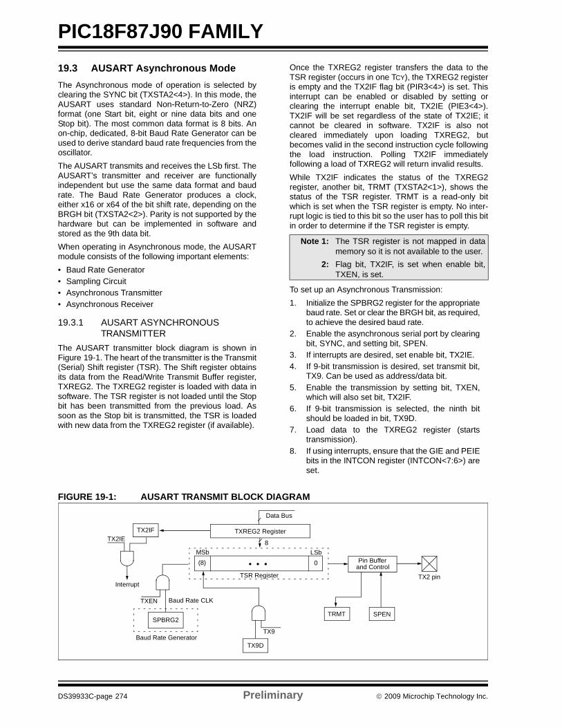
PIC18F87J90 FAMILY
DS39933C-page 274 Preliminary © 2009 Microchip Technology Inc.
19.3 AUSART Asynchronous ModeThe Asynchronous mode of operation is selected byclearing the SYNC bit (TXSTA2<4>). In this mode, theAUSART uses standard Non-Return-to-Zero (NRZ)format (one Start bit, eight or nine data bits and oneStop bit). The most common data format is 8 bits. Anon-chip, dedicated, 8-bit Baud Rate Generator can beused to derive standard baud rate frequencies from theoscillator. The AUSART transmits and receives the LSb first. TheAUSART’s transmitter and receiver are functionallyindependent but use the same data format and baudrate. The Baud Rate Generator produces a clock,either x16 or x64 of the bit shift rate, depending on theBRGH bit (TXSTA2<2>). Parity is not supported by thehardware but can be implemented in software andstored as the 9th data bit.When operating in Asynchronous mode, the AUSARTmodule consists of the following important elements:• Baud Rate Generator• Sampling Circuit• Asynchronous Transmitter• Asynchronous Receiver
19.3.1 AUSART ASYNCHRONOUS TRANSMITTER
The AUSART transmitter block diagram is shown inFigure 19-1. The heart of the transmitter is the Transmit(Serial) Shift register (TSR). The Shift register obtainsits data from the Read/Write Transmit Buffer register,TXREG2. The TXREG2 register is loaded with data insoftware. The TSR register is not loaded until the Stopbit has been transmitted from the previous load. Assoon as the Stop bit is transmitted, the TSR is loadedwith new data from the TXREG2 register (if available).
Once the TXREG2 register transfers the data to theTSR register (occurs in one TCY), the TXREG2 registeris empty and the TX2IF flag bit (PIR3<4>) is set. Thisinterrupt can be enabled or disabled by setting orclearing the interrupt enable bit, TX2IE (PIE3<4>).TX2IF will be set regardless of the state of TX2IE; itcannot be cleared in software. TX2IF is also notcleared immediately upon loading TXREG2, butbecomes valid in the second instruction cycle followingthe load instruction. Polling TX2IF immediatelyfollowing a load of TXREG2 will return invalid results. While TX2IF indicates the status of the TXREG2register, another bit, TRMT (TXSTA2<1>), shows thestatus of the TSR register. TRMT is a read-only bitwhich is set when the TSR register is empty. No inter-rupt logic is tied to this bit so the user has to poll this bitin order to determine if the TSR register is empty.
To set up an Asynchronous Transmission:1. Initialize the SPBRG2 register for the appropriate
baud rate. Set or clear the BRGH bit, as required,to achieve the desired baud rate.
2. Enable the asynchronous serial port by clearingbit, SYNC, and setting bit, SPEN.
3. If interrupts are desired, set enable bit, TX2IE.4. If 9-bit transmission is desired, set transmit bit,
TX9. Can be used as address/data bit.5. Enable the transmission by setting bit, TXEN,
which will also set bit, TX2IF.6. If 9-bit transmission is selected, the ninth bit
should be loaded in bit, TX9D.7. Load data to the TXREG2 register (starts
transmission).8. If using interrupts, ensure that the GIE and PEIE
bits in the INTCON register (INTCON<7:6>) areset.
FIGURE 19-1: AUSART TRANSMIT BLOCK DIAGRAM
Note 1: The TSR register is not mapped in datamemory so it is not available to the user.
2: Flag bit, TX2IF, is set when enable bit,TXEN, is set.
TX2IFTX2IE
Interrupt
TXEN Baud Rate CLK
SPBRG2
Baud Rate GeneratorTX9D
MSb LSb
Data Bus
TXREG2 Register
TSR Register
(8) 0
TX9
TRMT SPEN
TX2 pin
Pin Bufferand Control
8
• • •
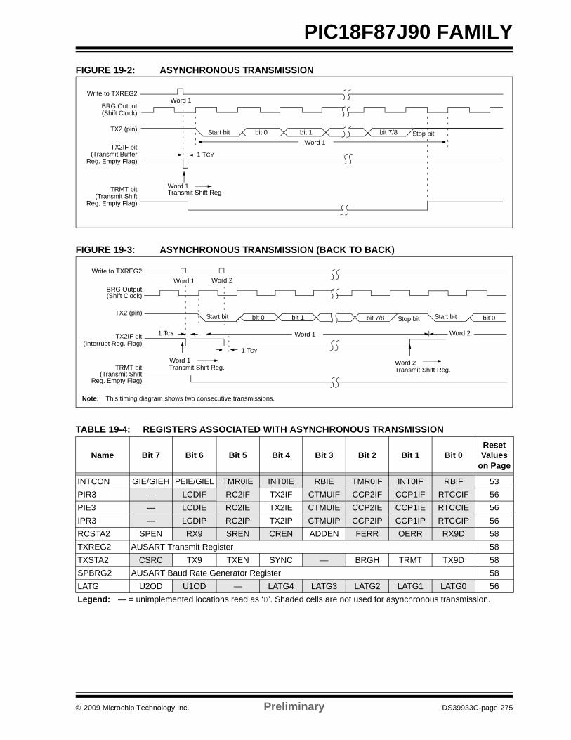
© 2009 Microchip Technology Inc. Preliminary DS39933C-page 275
PIC18F87J90 FAMILYFIGURE 19-2: ASYNCHRONOUS TRANSMISSION
FIGURE 19-3: ASYNCHRONOUS TRANSMISSION (BACK TO BACK)
TABLE 19-4: REGISTERS ASSOCIATED WITH ASYNCHRONOUS TRANSMISSION
Name Bit 7 Bit 6 Bit 5 Bit 4 Bit 3 Bit 2 Bit 1 Bit 0Reset Values
on Page
INTCON GIE/GIEH PEIE/GIEL TMR0IE INT0IE RBIE TMR0IF INT0IF RBIF 53PIR3 — LCDIF RC2IF TX2IF CTMUIF CCP2IF CCP1IF RTCCIF 56PIE3 — LCDIE RC2IE TX2IE CTMUIE CCP2IE CCP1IE RTCCIE 56IPR3 — LCDIP RC2IP TX2IP CTMUIP CCP2IP CCP1IP RTCCIP 56RCSTA2 SPEN RX9 SREN CREN ADDEN FERR OERR RX9D 58TXREG2 AUSART Transmit Register 58TXSTA2 CSRC TX9 TXEN SYNC — BRGH TRMT TX9D 58SPBRG2 AUSART Baud Rate Generator Register 58LATG U2OD U1OD — LATG4 LATG3 LATG2 LATG1 LATG0 56Legend: — = unimplemented locations read as ‘0’. Shaded cells are not used for asynchronous transmission.
Word 1
Word 1Transmit Shift Reg
Start bit bit 0 bit 1 bit 7/8
Write to TXREG2
BRG Output(Shift Clock)
TX2 (pin)
TX2IF bit(Transmit Buffer
Reg. Empty Flag)
TRMT bit(Transmit Shift
Reg. Empty Flag)
1 TCY
Word 1
Stop bit
Transmit Shift Reg.
Write to TXREG2
BRG Output(Shift Clock)
TX2 (pin)
TX2IF bit(Interrupt Reg. Flag)
TRMT bit(Transmit Shift
Reg. Empty Flag)
Word 1 Word 2
Word 1 Word 2
Stop bit Start bit
Transmit Shift Reg.
Word 1 Word 2
bit 0 bit 1 bit 7/8 bit 0
Note: This timing diagram shows two consecutive transmissions.
1 TCY
1 TCY
Start bit
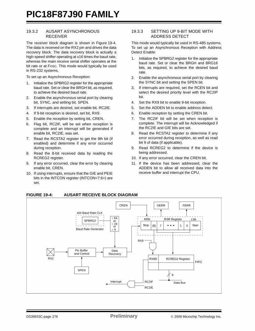
PIC18F87J90 FAMILY
DS39933C-page 276 Preliminary © 2009 Microchip Technology Inc.
19.3.2 AUSART ASYNCHRONOUS RECEIVER
The receiver block diagram is shown in Figure 19-4.The data is received on the RX2 pin and drives the datarecovery block. The data recovery block is actually ahigh-speed shifter operating at x16 times the baud rate,whereas the main receive serial shifter operates at thebit rate or at FOSC. This mode would typically be usedin RS-232 systems.
To set up an Asynchronous Reception:
1. Initialize the SPBRG2 register for the appropriatebaud rate. Set or clear the BRGH bit, as required,to achieve the desired baud rate.
2. Enable the asynchronous serial port by clearingbit, SYNC, and setting bit, SPEN.
3. If interrupts are desired, set enable bit, RC2IE.4. If 9-bit reception is desired, set bit, RX9.5. Enable the reception by setting bit, CREN.6. Flag bit, RC2IF, will be set when reception is
complete and an interrupt will be generated ifenable bit, RC2IE, was set.
7. Read the RCSTA2 register to get the 9th bit (ifenabled) and determine if any error occurredduring reception.
8. Read the 8-bit received data by reading theRCREG2 register.
9. If any error occurred, clear the error by clearingenable bit, CREN.
10. If using interrupts, ensure that the GIE and PEIEbits in the INTCON register (INTCON<7:6>) areset.
19.3.3 SETTING UP 9-BIT MODE WITH ADDRESS DETECT
This mode would typically be used in RS-485 systems.To set up an Asynchronous Reception with AddressDetect Enable:
1. Initialize the SPBRG2 register for the appropriatebaud rate. Set or clear the BRGH and BRG16bits, as required, to achieve the desired baudrate.
2. Enable the asynchronous serial port by clearingthe SYNC bit and setting the SPEN bit.
3. If interrupts are required, set the RCEN bit andselect the desired priority level with the RC2IPbit.
4. Set the RX9 bit to enable 9-bit reception. 5. Set the ADDEN bit to enable address detect.6. Enable reception by setting the CREN bit.7. The RC2IF bit will be set when reception is
complete. The interrupt will be Acknowledged ifthe RC2IE and GIE bits are set.
8. Read the RCSTA2 register to determine if anyerror occurred during reception, as well as readbit 9 of data (if applicable).
9. Read RCREG2 to determine if the device isbeing addressed.
10. If any error occurred, clear the CREN bit. 11. If the device has been addressed, clear the
ADDEN bit to allow all received data into thereceive buffer and interrupt the CPU.
FIGURE 19-4: AUSART RECEIVE BLOCK DIAGRAM
x64 Baud Rate CLK
Baud Rate Generator
RX2
Pin Bufferand Control
SPEN
DataRecovery
CREN OERR FERR
RSR RegisterMSb LSb
RX9D RCREG2 RegisterFIFO
Interrupt RC2IF
RC2IEData Bus
8
÷ 64
÷ 16or
Stop Start(8) 7 1 0
RX9
• • •
SPBRG2
or÷ 4
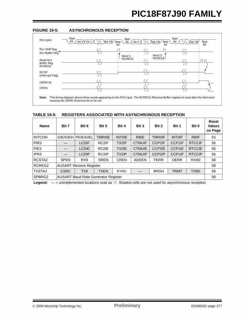
© 2009 Microchip Technology Inc. Preliminary DS39933C-page 277
PIC18F87J90 FAMILYFIGURE 19-5: ASYNCHRONOUS RECEPTION
TABLE 19-5: REGISTERS ASSOCIATED WITH ASYNCHRONOUS RECEPTION
Name Bit 7 Bit 6 Bit 5 Bit 4 Bit 3 Bit 2 Bit 1 Bit 0Reset Values
on Page
INTCON GIE/GIEH PEIE/GIEL TMR0IE INT0IE RBIE TMR0IF INT0IF RBIF 53PIR3 — LCDIF RC2IF TX2IF CTMUIF CCP2IF CCP1IF RTCCIF 56PIE3 — LCDIE RC2IE TX2IE CTMUIE CCP2IE CCP1IE RTCCIE 56IPR3 — LCDIP RC2IP TX2IP CTMUIP CCP2IP CCP1IP RTCCIP 56RCSTA2 SPEN RX9 SREN CREN ADDEN FERR OERR RX9D 58RCREG2 AUSART Receive Register 58TXSTA2 CSRC TX9 TXEN SYNC — BRGH TRMT TX9D 58SPBRG2 AUSART Baud Rate Generator Register 58Legend: — = unimplemented locations read as ‘0’. Shaded cells are not used for asynchronous reception.
Startbit bit 7/8bit 1bit 0 bit 7/8 bit 0Stop
bit
Startbit
Startbitbit 7/8 Stop
bitRX2 (pin)
Rcv Buffer RegRcv Shift Reg
Read RcvBuffer RegRCREG2
RC2IF(Interrupt Flag)
OERR bit
CREN
Word 1RCREG2
Word 2RCREG2
Stopbit
Note: This timing diagram shows three words appearing on the RX2 input. The RCREG2 (Receive Buffer register) is read after the third wordcausing the OERR (Overrun) bit to be set.
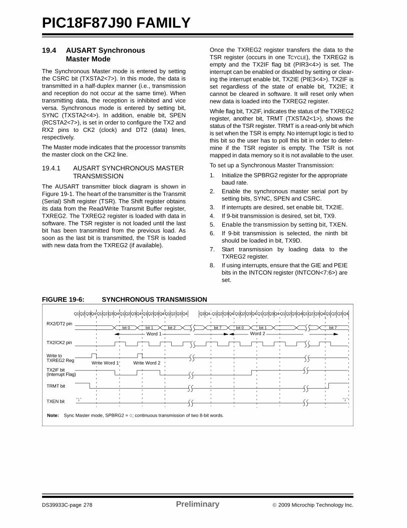
PIC18F87J90 FAMILY
DS39933C-page 278 Preliminary © 2009 Microchip Technology Inc.
19.4 AUSART Synchronous Master Mode
The Synchronous Master mode is entered by settingthe CSRC bit (TXSTA2<7>). In this mode, the data istransmitted in a half-duplex manner (i.e., transmissionand reception do not occur at the same time). Whentransmitting data, the reception is inhibited and viceversa. Synchronous mode is entered by setting bit,SYNC (TXSTA2<4>). In addition, enable bit, SPEN(RCSTA2<7>), is set in order to configure the TX2 andRX2 pins to CK2 (clock) and DT2 (data) lines,respectively.
The Master mode indicates that the processor transmitsthe master clock on the CK2 line.
19.4.1 AUSART SYNCHRONOUS MASTER TRANSMISSION
The AUSART transmitter block diagram is shown inFigure 19-1. The heart of the transmitter is the Transmit(Serial) Shift register (TSR). The Shift register obtainsits data from the Read/Write Transmit Buffer register,TXREG2. The TXREG2 register is loaded with data insoftware. The TSR register is not loaded until the lastbit has been transmitted from the previous load. Assoon as the last bit is transmitted, the TSR is loadedwith new data from the TXREG2 (if available).
Once the TXREG2 register transfers the data to theTSR register (occurs in one TCYCLE), the TXREG2 isempty and the TX2IF flag bit (PIR3<4>) is set. Theinterrupt can be enabled or disabled by setting or clear-ing the interrupt enable bit, TX2IE (PIE3<4>). TX2IF isset regardless of the state of enable bit, TX2IE; itcannot be cleared in software. It will reset only whennew data is loaded into the TXREG2 register.
While flag bit, TX2IF, indicates the status of the TXREG2register, another bit, TRMT (TXSTA2<1>), shows thestatus of the TSR register. TRMT is a read-only bit whichis set when the TSR is empty. No interrupt logic is tied tothis bit so the user has to poll this bit in order to deter-mine if the TSR register is empty. The TSR is notmapped in data memory so it is not available to the user.
To set up a Synchronous Master Transmission:
1. Initialize the SPBRG2 register for the appropriatebaud rate.
2. Enable the synchronous master serial port bysetting bits, SYNC, SPEN and CSRC.
3. If interrupts are desired, set enable bit, TX2IE.4. If 9-bit transmission is desired, set bit, TX9.5. Enable the transmission by setting bit, TXEN.6. If 9-bit transmission is selected, the ninth bit
should be loaded in bit, TX9D.7. Start transmission by loading data to the
TXREG2 register.8. If using interrupts, ensure that the GIE and PEIE
bits in the INTCON register (INTCON<7:6>) areset.
FIGURE 19-6: SYNCHRONOUS TRANSMISSION
bit 0 bit 1 bit 7Word 1
Q1 Q2 Q3Q4 Q1 Q2 Q3 Q4 Q1 Q2 Q3 Q4 Q1Q2 Q3 Q4 Q1 Q2 Q3 Q4 Q3 Q4 Q1 Q2 Q3Q4 Q1Q2 Q3Q4 Q1 Q2Q3Q4 Q1 Q2Q3 Q4Q1 Q2 Q3 Q4 Q1 Q2 Q3 Q4
bit 2 bit 0 bit 1 bit 7RX2/DT2 pin
TX2/CK2 pin
Write toTXREG2 Reg
TX2IF bit(Interrupt Flag)
TXEN bit ‘1’ ‘1’
Word 2
TRMT bit
Write Word 1 Write Word 2
Note: Sync Master mode, SPBRG2 = 0; continuous transmission of two 8-bit words.
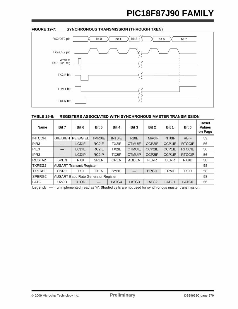
© 2009 Microchip Technology Inc. Preliminary DS39933C-page 279
PIC18F87J90 FAMILYFIGURE 19-7: SYNCHRONOUS TRANSMISSION (THROUGH TXEN)
TABLE 19-6: REGISTERS ASSOCIATED WITH SYNCHRONOUS MASTER TRANSMISSION
Name Bit 7 Bit 6 Bit 5 Bit 4 Bit 3 Bit 2 Bit 1 Bit 0Reset Values
on Page
INTCON GIE/GIEH PEIE/GIEL TMR0IE INT0IE RBIE TMR0IF INT0IF RBIF 53PIR3 — LCDIF RC2IF TX2IF CTMUIF CCP2IF CCP1IF RTCCIF 56PIE3 — LCDIE RC2IE TX2IE CTMUIE CCP2IE CCP1IE RTCCIE 56IPR3 — LCDIP RC2IP TX2IP CTMUIP CCP2IP CCP1IP RTCCIP 56RCSTA2 SPEN RX9 SREN CREN ADDEN FERR OERR RX9D 58TXREG2 AUSART Transmit Register 58TXSTA2 CSRC TX9 TXEN SYNC — BRGH TRMT TX9D 58SPBRG2 AUSART Baud Rate Generator Register 58LATG U2OD U1OD — LATG4 LATG3 LATG2 LATG1 LATG0 56Legend: — = unimplemented, read as ‘0’. Shaded cells are not used for synchronous master transmission.
RX2/DT2 pin
TX2/CK2 pin
Write toTXREG2 Reg
TX2IF bit
TRMT bit
bit 0 bit 1 bit 2 bit 6 bit 7
TXEN bit
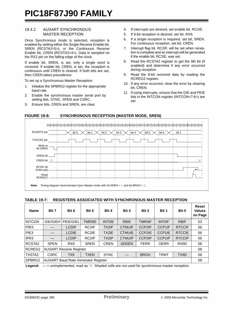
PIC18F87J90 FAMILY
DS39933C-page 280 Preliminary © 2009 Microchip Technology Inc.
19.4.2 AUSART SYNCHRONOUS MASTER RECEPTION
Once Synchronous mode is selected, reception isenabled by setting either the Single Receive Enable bit,SREN (RCSTA2<5>), or the Continuous ReceiveEnable bit, CREN (RCSTA2<4>). Data is sampled onthe RX2 pin on the falling edge of the clock.If enable bit, SREN, is set, only a single word isreceived. If enable bit, CREN, is set, the reception iscontinuous until CREN is cleared. If both bits are set,then CREN takes precedence.To set up a Synchronous Master Reception:1. Initialize the SPBRG2 register for the appropriate
baud rate.2. Enable the synchronous master serial port by
setting bits, SYNC, SPEN and CSRC.3. Ensure bits, CREN and SREN, are clear.
4. If interrupts are desired, set enable bit, RC2IE.5. If 9-bit reception is desired, set bit, RX9.6. If a single reception is required, set bit, SREN.
For continuous reception, set bit, CREN.7. Interrupt flag bit, RC2IF, will be set when recep-
tion is complete and an interrupt will be generatedif the enable bit, RC2IE, was set.
8. Read the RCSTA2 register to get the 9th bit (ifenabled) and determine if any error occurredduring reception.
9. Read the 8-bit received data by reading theRCREG2 register.
10. If any error occurred, clear the error by clearingbit, CREN.
11. If using interrupts, ensure that the GIE and PEIEbits in the INTCON register (INTCON<7:6>) areset.
FIGURE 19-8: SYNCHRONOUS RECEPTION (MASTER MODE, SREN)
TABLE 19-7: REGISTERS ASSOCIATED WITH SYNCHRONOUS MASTER RECEPTION
Name Bit 7 Bit 6 Bit 5 Bit 4 Bit 3 Bit 2 Bit 1 Bit 0Reset Values
on Page
INTCON GIE/GIEH PEIE/GIEL TMR0IE INT0IE RBIE TMR0IF INT0IF RBIF 53PIR3 — LCDIF RC2IF TX2IF CTMUIF CCP2IF CCP1IF RTCCIF 56PIE3 — LCDIE RC2IE TX2IE CTMUIE CCP2IE CCP1IE RTCCIE 56IPR3 — LCDIP RC2IP TX2IP CTMUIP CCP2IP CCP1IP RTCCIP 56RCSTA2 SPEN RX9 SREN CREN ADDEN FERR OERR RX9D 58RCREG2 AUSART Receive Register 58TXSTA2 CSRC TX9 TXEN SYNC — BRGH TRMT TX9D 58SPBRG2 AUSART Baud Rate Generator Register 58Legend: — = unimplemented, read as ‘0’. Shaded cells are not used for synchronous master reception.
CREN bit
RX2/DT2 pin
TX2/CK2 pin
Write tobit SREN
SREN bit
RC2IF bit(Interrupt)
ReadRCREG2
Q3 Q4 Q1 Q2 Q3 Q4 Q1 Q2 Q3 Q4Q2 Q1 Q2 Q3 Q4 Q1 Q2 Q3 Q4 Q1 Q2 Q3 Q4 Q1 Q2 Q3 Q4 Q1Q2 Q3 Q4 Q1 Q2 Q3 Q4 Q1 Q2 Q3 Q4
‘0’
bit 0 bit 1 bit 2 bit 3 bit 4 bit 5 bit 6 bit 7
‘0’
Q1 Q2 Q3 Q4
Note: Timing diagram demonstrates Sync Master mode with bit SREN = 1 and bit BRGH = 0.
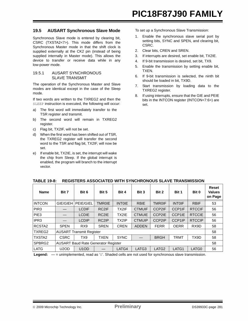
© 2009 Microchip Technology Inc. Preliminary DS39933C-page 281
PIC18F87J90 FAMILY19.5 AUSART Synchronous Slave ModeSynchronous Slave mode is entered by clearing bit,CSRC (TXSTA2<7>). This mode differs from theSynchronous Master mode in that the shift clock issupplied externally at the CK2 pin (instead of beingsupplied internally in Master mode). This allows thedevice to transfer or receive data while in anylow-power mode.
19.5.1 AUSART SYNCHRONOUS SLAVE TRANSMIT
The operation of the Synchronous Master and Slavemodes are identical except in the case of the Sleepmode.
If two words are written to the TXREG2 and then theSLEEP instruction is executed, the following will occur:
a) The first word will immediately transfer to theTSR register and transmit.
b) The second word will remain in TXREG2register.
c) Flag bit, TX2IF, will not be set. d) When the first word has been shifted out of TSR,
the TXREG2 register will transfer the secondword to the TSR and flag bit, TX2IF, will now beset.
e) If enable bit, TX2IE, is set, the interrupt will wakethe chip from Sleep. If the global interrupt isenabled, the program will branch to the interruptvector.
To set up a Synchronous Slave Transmission:
1. Enable the synchronous slave serial port bysetting bits, SYNC and SPEN, and clearing bit,CSRC.
2. Clear bits, CREN and SREN.3. If interrupts are desired, set enable bit, TX2IE.4. If 9-bit transmission is desired, set bit, TX9.5. Enable the transmission by setting enable bit,
TXEN.6. If 9-bit transmission is selected, the ninth bit
should be loaded in bit, TX9D.7. Start transmission by loading data to the
TXREG2 register.8. If using interrupts, ensure that the GIE and PEIE
bits in the INTCON register (INTCON<7:6>) areset.
TABLE 19-8: REGISTERS ASSOCIATED WITH SYNCHRONOUS SLAVE TRANSMISSION
Name Bit 7 Bit 6 Bit 5 Bit 4 Bit 3 Bit 2 Bit 1 Bit 0Reset Values
on Page
INTCON GIE/GIEH PEIE/GIEL TMR0IE INT0IE RBIE TMR0IF INT0IF RBIF 53PIR3 — LCDIF RC2IF TX2IF CTMUIF CCP2IF CCP1IF RTCCIF 56PIE3 — LCDIE RC2IE TX2IE CTMUIE CCP2IE CCP1IE RTCCIE 56IPR3 — LCDIP RC2IP TX2IP CTMUIP CCP2IP CCP1IP RTCCIP 56RCSTA2 SPEN RX9 SREN CREN ADDEN FERR OERR RX9D 58TXREG2 AUSART Transmit Register 58TXSTA2 CSRC TX9 TXEN SYNC — BRGH TRMT TX9D 58SPBRG2 AUSART Baud Rate Generator Register 58LATG U2OD U1OD — LATG4 LATG3 LATG2 LATG1 LATG0 56Legend: — = unimplemented, read as ‘0’. Shaded cells are not used for synchronous slave transmission.
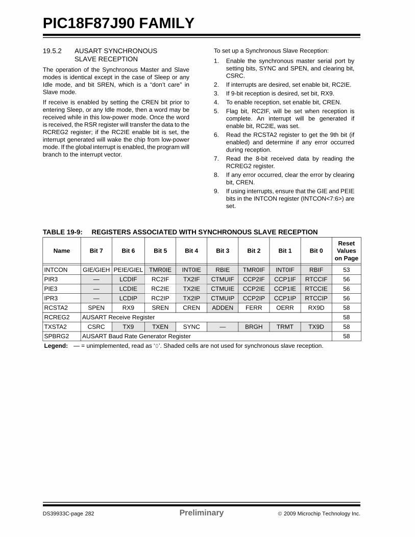
PIC18F87J90 FAMILY
DS39933C-page 282 Preliminary © 2009 Microchip Technology Inc.
19.5.2 AUSART SYNCHRONOUS SLAVE RECEPTION
The operation of the Synchronous Master and Slavemodes is identical except in the case of Sleep or anyIdle mode, and bit SREN, which is a “don’t care” inSlave mode.
If receive is enabled by setting the CREN bit prior toentering Sleep, or any Idle mode, then a word may bereceived while in this low-power mode. Once the wordis received, the RSR register will transfer the data to theRCREG2 register; if the RC2IE enable bit is set, theinterrupt generated will wake the chip from low-powermode. If the global interrupt is enabled, the program willbranch to the interrupt vector.
To set up a Synchronous Slave Reception:
1. Enable the synchronous master serial port bysetting bits, SYNC and SPEN, and clearing bit,CSRC.
2. If interrupts are desired, set enable bit, RC2IE.3. If 9-bit reception is desired, set bit, RX9.4. To enable reception, set enable bit, CREN.5. Flag bit, RC2IF, will be set when reception is
complete. An interrupt will be generated ifenable bit, RC2IE, was set.
6. Read the RCSTA2 register to get the 9th bit (ifenabled) and determine if any error occurredduring reception.
7. Read the 8-bit received data by reading theRCREG2 register.
8. If any error occurred, clear the error by clearingbit, CREN.
9. If using interrupts, ensure that the GIE and PEIEbits in the INTCON register (INTCON<7:6>) areset.
TABLE 19-9: REGISTERS ASSOCIATED WITH SYNCHRONOUS SLAVE RECEPTION
Name Bit 7 Bit 6 Bit 5 Bit 4 Bit 3 Bit 2 Bit 1 Bit 0Reset Values
on Page
INTCON GIE/GIEH PEIE/GIEL TMR0IE INT0IE RBIE TMR0IF INT0IF RBIF 53PIR3 — LCDIF RC2IF TX2IF CTMUIF CCP2IF CCP1IF RTCCIF 56PIE3 — LCDIE RC2IE TX2IE CTMUIE CCP2IE CCP1IE RTCCIE 56IPR3 — LCDIP RC2IP TX2IP CTMUIP CCP2IP CCP1IP RTCCIP 56RCSTA2 SPEN RX9 SREN CREN ADDEN FERR OERR RX9D 58RCREG2 AUSART Receive Register 58TXSTA2 CSRC TX9 TXEN SYNC — BRGH TRMT TX9D 58SPBRG2 AUSART Baud Rate Generator Register 58Legend: — = unimplemented, read as ‘0’. Shaded cells are not used for synchronous slave reception.
© 2009 Microchip Technology Inc. Preliminary DS39933C-page 283
PIC18F87J90 FAMILY
20.0 10-BIT ANALOG-TO-DIGITAL CONVERTER (A/D) MODULE
The Analog-to-Digital (A/D) converter module has12 inputs for all PIC18F87J90 family devices. Thismodule allows conversion of an analog input signal toa corresponding 10-bit digital number.
The module has five registers:
• A/D Result High Register (ADRESH)• A/D Result Low Register (ADRESL)• A/D Control Register 0 (ADCON0)• A/D Control Register 1 (ADCON1)• A/D Control Register 2 (ADCON2)
The ADCON0 register, shown in Register 20-1,controls the operation of the A/D module. TheADCON1 register, shown in Register 20-2, configuresthe functions of the port pins. The ADCON2 register,shown in Register 20-3, configures the A/D clocksource, programmed acquisition time and justification.
REGISTER 20-1: ADCON0: A/D CONTROL REGISTER 0
R/W-0 U-0 R/W-0 R/W-0 R/W-0 R/W-0 R/W-0 R/W-0
ADCAL — CHS3 CHS2 CHS1 CHS0 GO/DONE ADONbit 7 bit 0
Legend:R = Readable bit W = Writable bit U = Unimplemented bit, read as ‘0’-n = Value at POR ‘1’ = Bit is set ‘0’ = Bit is cleared x = Bit is unknown
bit 7 ADCAL: A/D Calibration bit1 = Calibration is performed on next A/D conversion 0 = Normal A/D converter operation (no calibration is performed)
bit 6 Unimplemented: Read as ‘0’bit 5-2 CHS<3:0>: Analog Channel Select bits
0000 = Channel 00 (AN0)0001 = Channel 01 (AN1)0010 = Channel 02 (AN2)0011 = Channel 03 (AN3)0100 = Channel 04 (AN4)0101 = Channel 05 (AN5)0110 = Channel 06 (AN6)0111 = Channel 07 (AN7)1000 = Channel 08 (AN8)1001 = Channel 09 (AN9)1010 = Channel 10 (AN10)1011 = Channel 11 (AN11)11xx = Unused
bit 1 GO/DONE: A/D Conversion Status bitWhen ADON = 1: 1 = A/D conversion in progress0 = A/D Idle
bit 0 ADON: A/D On bit1 = A/D converter module is enabled 0 = A/D converter module is disabled
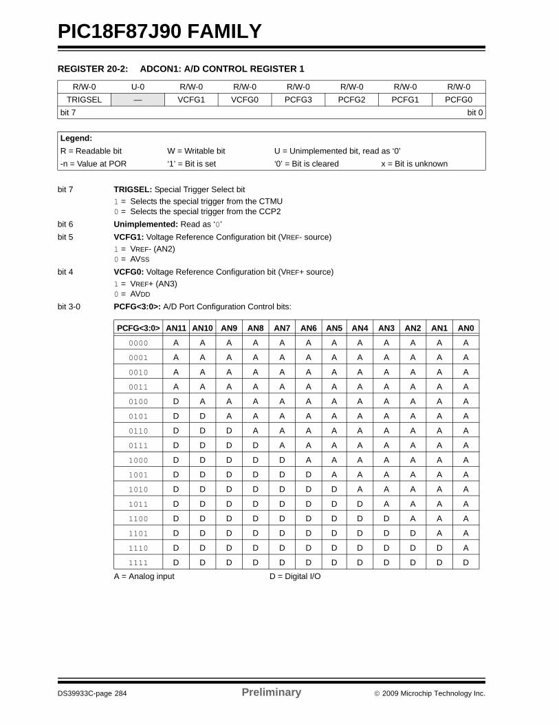
PIC18F87J90 FAMILY
DS39933C-page 284 Preliminary © 2009 Microchip Technology Inc.
REGISTER 20-2: ADCON1: A/D CONTROL REGISTER 1
R/W-0 U-0 R/W-0 R/W-0 R/W-0 R/W-0 R/W-0 R/W-0TRIGSEL — VCFG1 VCFG0 PCFG3 PCFG2 PCFG1 PCFG0
bit 7 bit 0
Legend:R = Readable bit W = Writable bit U = Unimplemented bit, read as ‘0’-n = Value at POR ‘1’ = Bit is set ‘0’ = Bit is cleared x = Bit is unknown
bit 7 TRIGSEL: Special Trigger Select bit1 = Selects the special trigger from the CTMU0 = Selects the special trigger from the CCP2
bit 6 Unimplemented: Read as ‘0’bit 5 VCFG1: Voltage Reference Configuration bit (VREF- source)
1 = VREF- (AN2)0 = AVSS
bit 4 VCFG0: Voltage Reference Configuration bit (VREF+ source)1 = VREF+ (AN3)0 = AVDD
bit 3-0 PCFG<3:0>: A/D Port Configuration Control bits:
A = Analog input D = Digital I/O
PCFG<3:0> AN11 AN10 AN9 AN8 AN7 AN6 AN5 AN4 AN3 AN2 AN1 AN0
0000 A A A A A A A A A A A A
0001 A A A A A A A A A A A A
0010 A A A A A A A A A A A A
0011 A A A A A A A A A A A A
0100 D A A A A A A A A A A A
0101 D D A A A A A A A A A A
0110 D D D A A A A A A A A A
0111 D D D D A A A A A A A A
1000 D D D D D A A A A A A A
1001 D D D D D D A A A A A A
1010 D D D D D D D A A A A A
1011 D D D D D D D D A A A A
1100 D D D D D D D D D A A A
1101 D D D D D D D D D D A A
1110 D D D D D D D D D D D A
1111 D D D D D D D D D D D D
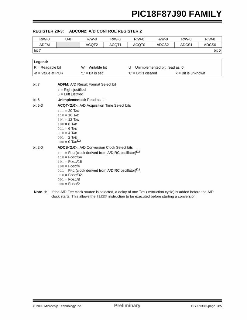
© 2009 Microchip Technology Inc. Preliminary DS39933C-page 285
PIC18F87J90 FAMILY REGISTER 20-3: ADCON2: A/D CONTROL REGISTER 2
R/W-0 U-0 R/W-0 R/W-0 R/W-0 R/W-0 R/W-0 R/W-0ADFM — ACQT2 ACQT1 ACQT0 ADCS2 ADCS1 ADCS0
bit 7 bit 0
Legend:R = Readable bit W = Writable bit U = Unimplemented bit, read as ‘0’-n = Value at POR ‘1’ = Bit is set ‘0’ = Bit is cleared x = Bit is unknown
bit 7 ADFM: A/D Result Format Select bit1 = Right justified 0 = Left justified
bit 6 Unimplemented: Read as ‘0’bit 5-3 ACQT<2:0>: A/D Acquisition Time Select bits
111 = 20 TAD110 = 16 TAD101 = 12 TAD100 = 8 TAD011 = 6 TAD010 = 4 TAD001 = 2 TAD000 = 0 TAD(1)
bit 2-0 ADCS<2:0>: A/D Conversion Clock Select bits111 = FRC (clock derived from A/D RC oscillator)(1) 110 = FOSC/64 101 = FOSC/16 100 = FOSC/4 011 = FRC (clock derived from A/D RC oscillator)(1) 010 = FOSC/32 001 = FOSC/8 000 = FOSC/2
Note 1: If the A/D FRC clock source is selected, a delay of one TCY (instruction cycle) is added before the A/D clock starts. This allows the SLEEP instruction to be executed before starting a conversion.
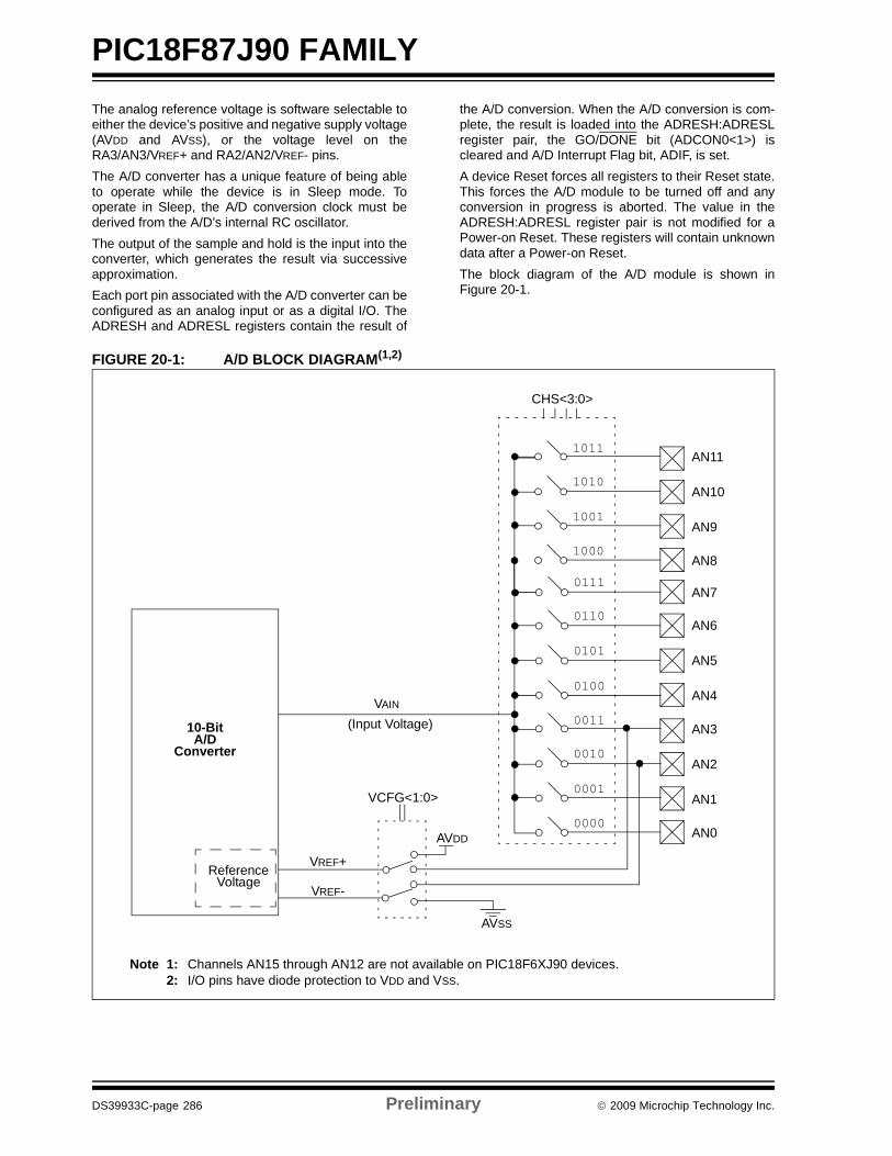
PIC18F87J90 FAMILY
DS39933C-page 286 Preliminary © 2009 Microchip Technology Inc.
The analog reference voltage is software selectable toeither the device’s positive and negative supply voltage(AVDD and AVSS), or the voltage level on theRA3/AN3/VREF+ and RA2/AN2/VREF- pins.The A/D converter has a unique feature of being ableto operate while the device is in Sleep mode. Tooperate in Sleep, the A/D conversion clock must bederived from the A/D’s internal RC oscillator.The output of the sample and hold is the input into theconverter, which generates the result via successiveapproximation.Each port pin associated with the A/D converter can beconfigured as an analog input or as a digital I/O. TheADRESH and ADRESL registers contain the result of
the A/D conversion. When the A/D conversion is com-plete, the result is loaded into the ADRESH:ADRESLregister pair, the GO/DONE bit (ADCON0<1>) iscleared and A/D Interrupt Flag bit, ADIF, is set. A device Reset forces all registers to their Reset state.This forces the A/D module to be turned off and anyconversion in progress is aborted. The value in theADRESH:ADRESL register pair is not modified for aPower-on Reset. These registers will contain unknowndata after a Power-on Reset.The block diagram of the A/D module is shown inFigure 20-1.
FIGURE 20-1: A/D BLOCK DIAGRAM(1,2)
(Input Voltage)VAIN
VREF+ReferenceVoltage
AVDD
VCFG<1:0>
CHS<3:0>
AN7
AN6
AN4
AN3
AN2
AN1
AN0
0111
0110
0100
0011
0010
0001
0000
10-BitA/D
VREF-
AVSS
Converter
AN11
AN10
AN9
AN8
1011
1010
1001
1000
Note 1: Channels AN15 through AN12 are not available on PIC18F6XJ90 devices.2: I/O pins have diode protection to VDD and VSS.
AN50101
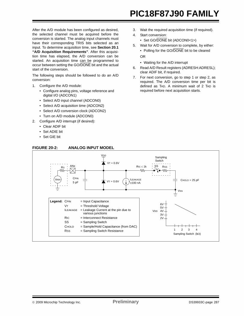
© 2009 Microchip Technology Inc. Preliminary DS39933C-page 287
PIC18F87J90 FAMILYAfter the A/D module has been configured as desired,the selected channel must be acquired before theconversion is started. The analog input channels musthave their corresponding TRIS bits selected as aninput. To determine acquisition time, see Section 20.1“A/D Acquisition Requirements”. After this acquisi-tion time has elapsed, the A/D conversion can bestarted. An acquisition time can be programmed tooccur between setting the GO/DONE bit and the actualstart of the conversion.
The following steps should be followed to do an A/Dconversion:
1. Configure the A/D module:• Configure analog pins, voltage reference and
digital I/O (ADCON1)• Select A/D input channel (ADCON0)• Select A/D acquisition time (ADCON2)• Select A/D conversion clock (ADCON2)• Turn on A/D module (ADCON0)
2. Configure A/D interrupt (if desired):• Clear ADIF bit • Set ADIE bit • Set GIE bit
3. Wait the required acquisition time (if required).4. Start conversion:
• Set GO/DONE bit (ADCON0<1>)5. Wait for A/D conversion to complete, by either:
• Polling for the GO/DONE bit to be cleared
OR
• Waiting for the A/D interrupt6. Read A/D Result registers (ADRESH:ADRESL);
clear ADIF bit, if required.7. For next conversion, go to step 1 or step 2, as
required. The A/D conversion time per bit isdefined as TAD. A minimum wait of 2 TAD isrequired before next acquisition starts.
FIGURE 20-2: ANALOG INPUT MODEL
VAIN CPIN
RS ANx
5 pF
VDD
VT = 0.6V
VT = 0.6VILEAKAGE
RIC ≤ 1k
SamplingSwitch
SS RSS
CHOLD = 25 pF
VSS
6V
Sampling Switch
5V4V3V2V
1 2 3 4(kΩ)
VDD
±100 nA
Legend: CPIN
VTILEAKAGE
RIC
SSCHOLD
= Input Capacitance= Threshold Voltage= Leakage Current at the pin due to
= Interconnect Resistance= Sampling Switch= Sample/Hold Capacitance (from DAC)
various junctions
= Sampling Switch ResistanceRSS
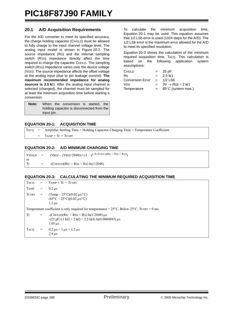
PIC18F87J90 FAMILY
DS39933C-page 288 Preliminary © 2009 Microchip Technology Inc.
20.1 A/D Acquisition RequirementsFor the A/D converter to meet its specified accuracy,the charge holding capacitor (CHOLD) must be allowedto fully charge to the input channel voltage level. Theanalog input model is shown in Figure 20-2. Thesource impedance (RS) and the internal samplingswitch (RSS) impedance directly affect the timerequired to charge the capacitor CHOLD. The samplingswitch (RSS) impedance varies over the device voltage(VDD). The source impedance affects the offset voltageat the analog input (due to pin leakage current). Themaximum recommended impedance for analogsources is 2.5 kΩ. After the analog input channel isselected (changed), the channel must be sampled forat least the minimum acquisition time before starting aconversion.
To calculate the minimum acquisition time,Equation 20-1 may be used. This equation assumesthat 1/2 LSb error is used (1024 steps for the A/D). The1/2 LSb error is the maximum error allowed for the A/Dto meet its specified resolution.
Equation 20-3 shows the calculation of the minimumrequired acquisition time, TACQ. This calculation isbased on the following application systemassumptions:
CHOLD = 25 pF Rs = 2.5 kΩ Conversion Error ≤ 1/2 LSb VDD = 3V → Rss = 2 kΩ Temperature = 85°C (system max.)
EQUATION 20-1: ACQUISITION TIME
EQUATION 20-2: A/D MINIMUM CHARGING TIME
EQUATION 20-3: CALCULATING THE MINIMUM REQUIRED ACQUISITION TIME
Note: When the conversion is started, theholding capacitor is disconnected from theinput pin.
TACQ = Amplifier Settling Time + Holding Capacitor Charging Time + Temperature Coefficient
= TAMP + TC + TCOFF
VHOLD = (VREF – (VREF/2048)) • (1 – e(-TC/CHOLD(RIC + RSS + RS))) or TC = -(CHOLD)(RIC + RSS + RS) ln(1/2048)
TACQ = TAMP + TC + TCOFF
TAMP = 0.2 μs
TCOFF = (Temp – 25°C)(0.02 μs/°C)(85°C – 25°C)(0.02 μs/°C)1.2 μs
Temperature coefficient is only required for temperatures > 25°C. Below 25°C, TCOFF = 0 ms.
TC = -(CHOLD)(RIC + RSS + RS) ln(1/2048) μs-(25 pF) (1 kΩ + 2 kΩ + 2.5 kΩ) ln(0.0004883) μs 1.05 μs
TACQ = 0.2 μs + 1 μs + 1.2 μs2.4 μs
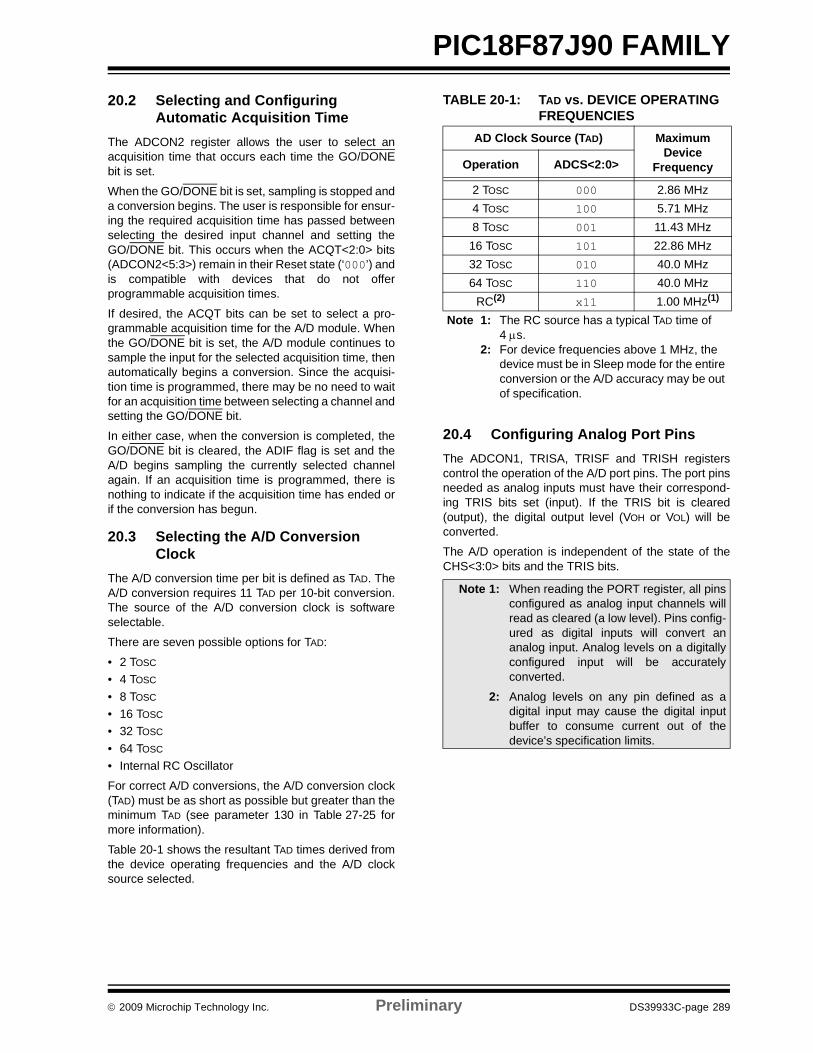
© 2009 Microchip Technology Inc. Preliminary DS39933C-page 289
PIC18F87J90 FAMILY20.2 Selecting and Configuring
Automatic Acquisition TimeThe ADCON2 register allows the user to select anacquisition time that occurs each time the GO/DONEbit is set.
When the GO/DONE bit is set, sampling is stopped anda conversion begins. The user is responsible for ensur-ing the required acquisition time has passed betweenselecting the desired input channel and setting theGO/DONE bit. This occurs when the ACQT<2:0> bits(ADCON2<5:3>) remain in their Reset state (‘000’) andis compatible with devices that do not offerprogrammable acquisition times.
If desired, the ACQT bits can be set to select a pro-grammable acquisition time for the A/D module. Whenthe GO/DONE bit is set, the A/D module continues tosample the input for the selected acquisition time, thenautomatically begins a conversion. Since the acquisi-tion time is programmed, there may be no need to waitfor an acquisition time between selecting a channel andsetting the GO/DONE bit.
In either case, when the conversion is completed, theGO/DONE bit is cleared, the ADIF flag is set and theA/D begins sampling the currently selected channelagain. If an acquisition time is programmed, there isnothing to indicate if the acquisition time has ended orif the conversion has begun.
20.3 Selecting the A/D Conversion Clock
The A/D conversion time per bit is defined as TAD. TheA/D conversion requires 11 TAD per 10-bit conversion.The source of the A/D conversion clock is softwareselectable.
There are seven possible options for TAD:
• 2 TOSC
• 4 TOSC
• 8 TOSC
• 16 TOSC
• 32 TOSC • 64 TOSC
• Internal RC Oscillator
For correct A/D conversions, the A/D conversion clock(TAD) must be as short as possible but greater than theminimum TAD (see parameter 130 in Table 27-25 formore information).
Table 20-1 shows the resultant TAD times derived fromthe device operating frequencies and the A/D clocksource selected.
TABLE 20-1: TAD vs. DEVICE OPERATING FREQUENCIES
20.4 Configuring Analog Port PinsThe ADCON1, TRISA, TRISF and TRISH registerscontrol the operation of the A/D port pins. The port pinsneeded as analog inputs must have their correspond-ing TRIS bits set (input). If the TRIS bit is cleared(output), the digital output level (VOH or VOL) will beconverted.
The A/D operation is independent of the state of theCHS<3:0> bits and the TRIS bits.
AD Clock Source (TAD) Maximum Device
FrequencyOperation ADCS<2:0>
2 TOSC 000 2.86 MHz4 TOSC 100 5.71 MHz8 TOSC 001 11.43 MHz
16 TOSC 101 22.86 MHz32 TOSC 010 40.0 MHz64 TOSC 110 40.0 MHz
RC(2) x11 1.00 MHz(1)
Note 1: The RC source has a typical TAD time of 4 μs.
2: For device frequencies above 1 MHz, the device must be in Sleep mode for the entire conversion or the A/D accuracy may be out of specification.
Note 1: When reading the PORT register, all pinsconfigured as analog input channels willread as cleared (a low level). Pins config-ured as digital inputs will convert ananalog input. Analog levels on a digitallyconfigured input will be accuratelyconverted.
2: Analog levels on any pin defined as adigital input may cause the digital inputbuffer to consume current out of thedevice’s specification limits.
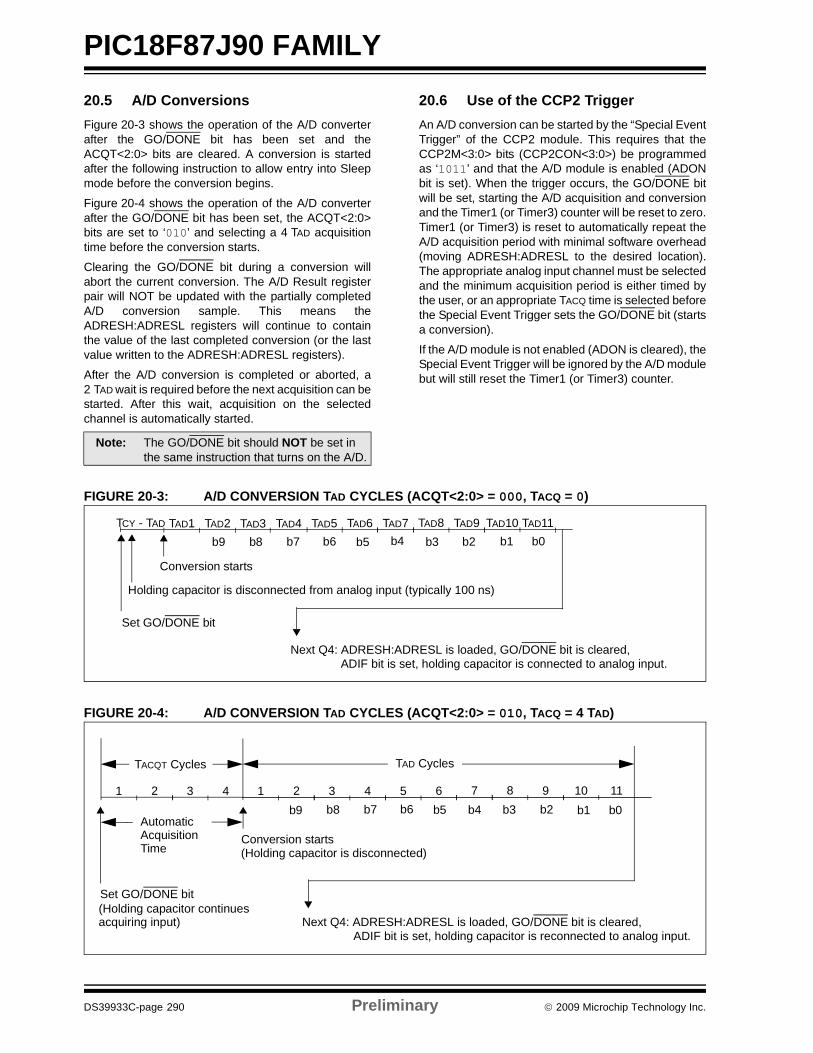
PIC18F87J90 FAMILY
DS39933C-page 290 Preliminary © 2009 Microchip Technology Inc.
20.5 A/D Conversions Figure 20-3 shows the operation of the A/D converterafter the GO/DONE bit has been set and theACQT<2:0> bits are cleared. A conversion is startedafter the following instruction to allow entry into Sleepmode before the conversion begins.
Figure 20-4 shows the operation of the A/D converterafter the GO/DONE bit has been set, the ACQT<2:0>bits are set to ‘010’ and selecting a 4 TAD acquisitiontime before the conversion starts.
Clearing the GO/DONE bit during a conversion willabort the current conversion. The A/D Result registerpair will NOT be updated with the partially completedA/D conversion sample. This means theADRESH:ADRESL registers will continue to containthe value of the last completed conversion (or the lastvalue written to the ADRESH:ADRESL registers).
After the A/D conversion is completed or aborted, a2 TAD wait is required before the next acquisition can bestarted. After this wait, acquisition on the selectedchannel is automatically started.
20.6 Use of the CCP2 TriggerAn A/D conversion can be started by the “Special EventTrigger” of the CCP2 module. This requires that theCCP2M<3:0> bits (CCP2CON<3:0>) be programmedas ‘1011’ and that the A/D module is enabled (ADONbit is set). When the trigger occurs, the GO/DONE bitwill be set, starting the A/D acquisition and conversionand the Timer1 (or Timer3) counter will be reset to zero.Timer1 (or Timer3) is reset to automatically repeat theA/D acquisition period with minimal software overhead(moving ADRESH:ADRESL to the desired location).The appropriate analog input channel must be selectedand the minimum acquisition period is either timed bythe user, or an appropriate TACQ time is selected beforethe Special Event Trigger sets the GO/DONE bit (startsa conversion).
If the A/D module is not enabled (ADON is cleared), theSpecial Event Trigger will be ignored by the A/D modulebut will still reset the Timer1 (or Timer3) counter.
FIGURE 20-3: A/D CONVERSION TAD CYCLES (ACQT<2:0> = 000, TACQ = 0)
FIGURE 20-4: A/D CONVERSION TAD CYCLES (ACQT<2:0> = 010, TACQ = 4 TAD)
Note: The GO/DONE bit should NOT be set in the same instruction that turns on the A/D.
TAD1 TAD2 TAD3 TAD4 TAD5 TAD6 TAD7 TAD8 TAD11
Set GO/DONE bit
Holding capacitor is disconnected from analog input (typically 100 ns)
TAD9 TAD10TCY - TAD
Next Q4: ADRESH:ADRESL is loaded, GO/DONE bit is cleared, ADIF bit is set, holding capacitor is connected to analog input.
Conversion starts
b0b9 b6 b5 b4 b3 b2 b1b8 b7
1 2 3 4 5 6 7 8 11
Set GO/DONE bit
(Holding capacitor is disconnected)
9 10
Next Q4: ADRESH:ADRESL is loaded, GO/DONE bit is cleared, ADIF bit is set, holding capacitor is reconnected to analog input.
Conversion starts
1 2 3 4
(Holding capacitor continuesacquiring input)
TACQT Cycles TAD Cycles
AutomaticAcquisitionTime
b0b9 b6 b5 b4 b3 b2 b1b8 b7
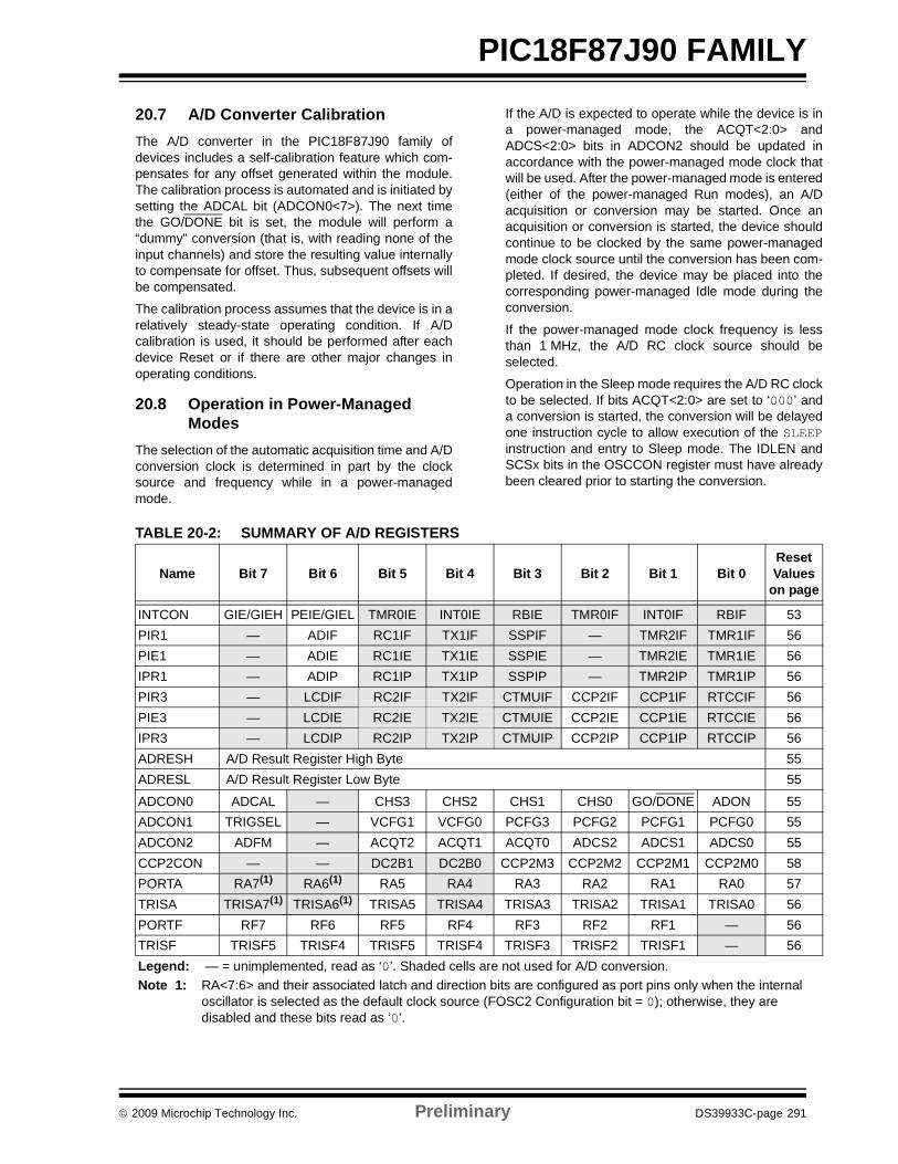
© 2009 Microchip Technology Inc. Preliminary DS39933C-page 291
PIC18F87J90 FAMILY
20.7 A/D Converter CalibrationThe A/D converter in the PIC18F87J90 family ofdevices includes a self-calibration feature which com-pensates for any offset generated within the module.The calibration process is automated and is initiated bysetting the ADCAL bit (ADCON0<7>). The next timethe GO/DONE bit is set, the module will perform a“dummy” conversion (that is, with reading none of theinput channels) and store the resulting value internallyto compensate for offset. Thus, subsequent offsets willbe compensated.
The calibration process assumes that the device is in arelatively steady-state operating condition. If A/Dcalibration is used, it should be performed after eachdevice Reset or if there are other major changes inoperating conditions.
20.8 Operation in Power-Managed Modes
The selection of the automatic acquisition time and A/Dconversion clock is determined in part by the clocksource and frequency while in a power-managedmode.
If the A/D is expected to operate while the device is ina power-managed mode, the ACQT<2:0> andADCS<2:0> bits in ADCON2 should be updated inaccordance with the power-managed mode clock thatwill be used. After the power-managed mode is entered(either of the power-managed Run modes), an A/Dacquisition or conversion may be started. Once anacquisition or conversion is started, the device shouldcontinue to be clocked by the same power-managedmode clock source until the conversion has been com-pleted. If desired, the device may be placed into thecorresponding power-managed Idle mode during theconversion.
If the power-managed mode clock frequency is lessthan 1 MHz, the A/D RC clock source should beselected.
Operation in the Sleep mode requires the A/D RC clockto be selected. If bits ACQT<2:0> are set to ‘000’ anda conversion is started, the conversion will be delayedone instruction cycle to allow execution of the SLEEPinstruction and entry to Sleep mode. The IDLEN andSCSx bits in the OSCCON register must have alreadybeen cleared prior to starting the conversion.
TABLE 20-2: SUMMARY OF A/D REGISTERS
Name Bit 7 Bit 6 Bit 5 Bit 4 Bit 3 Bit 2 Bit 1 Bit 0Reset Values
on page
INTCON GIE/GIEH PEIE/GIEL TMR0IE INT0IE RBIE TMR0IF INT0IF RBIF 53PIR1 — ADIF RC1IF TX1IF SSPIF — TMR2IF TMR1IF 56PIE1 — ADIE RC1IE TX1IE SSPIE — TMR2IE TMR1IE 56IPR1 — ADIP RC1IP TX1IP SSPIP — TMR2IP TMR1IP 56PIR3 — LCDIF RC2IF TX2IF CTMUIF CCP2IF CCP1IF RTCCIF 56PIE3 — LCDIE RC2IE TX2IE CTMUIE CCP2IE CCP1IE RTCCIE 56IPR3 — LCDIP RC2IP TX2IP CTMUIP CCP2IP CCP1IP RTCCIP 56ADRESH A/D Result Register High Byte 55ADRESL A/D Result Register Low Byte 55
ADCON0 ADCAL — CHS3 CHS2 CHS1 CHS0 GO/DONE ADON 55ADCON1 TRIGSEL — VCFG1 VCFG0 PCFG3 PCFG2 PCFG1 PCFG0 55ADCON2 ADFM — ACQT2 ACQT1 ACQT0 ADCS2 ADCS1 ADCS0 55CCP2CON — — DC2B1 DC2B0 CCP2M3 CCP2M2 CCP2M1 CCP2M0 58PORTA RA7(1) RA6(1) RA5 RA4 RA3 RA2 RA1 RA0 57TRISA TRISA7(1) TRISA6(1) TRISA5 TRISA4 TRISA3 TRISA2 TRISA1 TRISA0 56PORTF RF7 RF6 RF5 RF4 RF3 RF2 RF1 — 56TRISF TRISF5 TRISF4 TRISF5 TRISF4 TRISF3 TRISF2 TRISF1 — 56Legend: — = unimplemented, read as ‘0’. Shaded cells are not used for A/D conversion.Note 1: RA<7:6> and their associated latch and direction bits are configured as port pins only when the internal
oscillator is selected as the default clock source (FOSC2 Configuration bit = 0); otherwise, they are disabled and these bits read as ‘0’.

PIC18F87J90 FAMILY
DS39933C-page 292 Preliminary © 2009 Microchip Technology Inc.
NOTES:
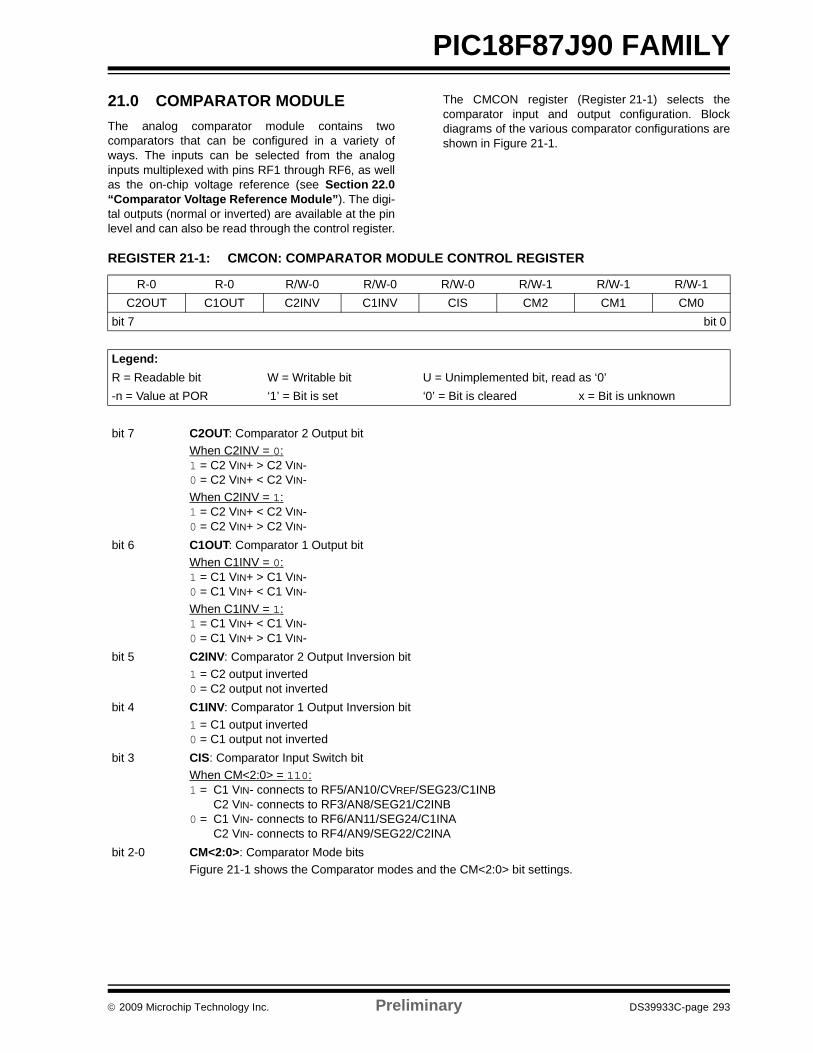
© 2009 Microchip Technology Inc. Preliminary DS39933C-page 293
PIC18F87J90 FAMILY
21.0 COMPARATOR MODULEThe analog comparator module contains twocomparators that can be configured in a variety ofways. The inputs can be selected from the analoginputs multiplexed with pins RF1 through RF6, as wellas the on-chip voltage reference (see Section 22.0“Comparator Voltage Reference Module”). The digi-tal outputs (normal or inverted) are available at the pinlevel and can also be read through the control register.
The CMCON register (Register 21-1) selects thecomparator input and output configuration. Blockdiagrams of the various comparator configurations areshown in Figure 21-1.
REGISTER 21-1: CMCON: COMPARATOR MODULE CONTROL REGISTER
R-0 R-0 R/W-0 R/W-0 R/W-0 R/W-1 R/W-1 R/W-1C2OUT C1OUT C2INV C1INV CIS CM2 CM1 CM0
bit 7 bit 0
Legend:R = Readable bit W = Writable bit U = Unimplemented bit, read as ‘0’-n = Value at POR ‘1’ = Bit is set ‘0’ = Bit is cleared x = Bit is unknown
bit 7 C2OUT: Comparator 2 Output bitWhen C2INV = 0:1 = C2 VIN+ > C2 VIN-0 = C2 VIN+ < C2 VIN-When C2INV = 1:1 = C2 VIN+ < C2 VIN-0 = C2 VIN+ > C2 VIN-
bit 6 C1OUT: Comparator 1 Output bitWhen C1INV = 0:1 = C1 VIN+ > C1 VIN-0 = C1 VIN+ < C1 VIN-When C1INV = 1:1 = C1 VIN+ < C1 VIN-0 = C1 VIN+ > C1 VIN-
bit 5 C2INV: Comparator 2 Output Inversion bit1 = C2 output inverted0 = C2 output not inverted
bit 4 C1INV: Comparator 1 Output Inversion bit1 = C1 output inverted0 = C1 output not inverted
bit 3 CIS: Comparator Input Switch bitWhen CM<2:0> = 110:1 = C1 VIN- connects to RF5/AN10/CVREF/SEG23/C1INB
C2 VIN- connects to RF3/AN8/SEG21/C2INB0 = C1 VIN- connects to RF6/AN11/SEG24/C1INA
C2 VIN- connects to RF4/AN9/SEG22/C2INAbit 2-0 CM<2:0>: Comparator Mode bits
Figure 21-1 shows the Comparator modes and the CM<2:0> bit settings.
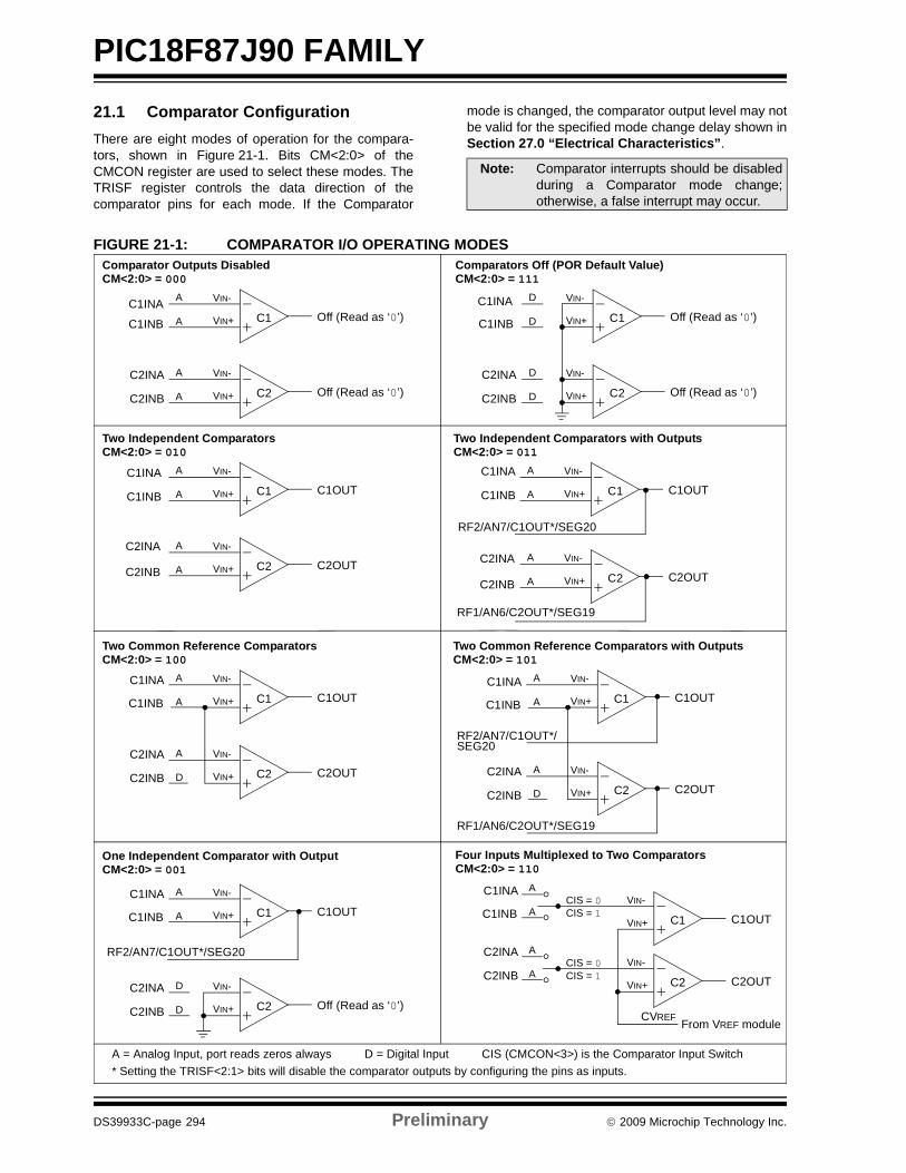
PIC18F87J90 FAMILY
DS39933C-page 294 Preliminary © 2009 Microchip Technology Inc.
21.1 Comparator ConfigurationThere are eight modes of operation for the compara-tors, shown in Figure 21-1. Bits CM<2:0> of theCMCON register are used to select these modes. TheTRISF register controls the data direction of thecomparator pins for each mode. If the Comparator
mode is changed, the comparator output level may notbe valid for the specified mode change delay shown inSection 27.0 “Electrical Characteristics”.
FIGURE 21-1: COMPARATOR I/O OPERATING MODES
Note: Comparator interrupts should be disabledduring a Comparator mode change;otherwise, a false interrupt may occur.
C1
VIN-
VIN+ Off (Read as ‘0’)
Comparator Outputs Disabled
A
A
CM<2:0> = 000
C2
VIN-
VIN+ Off (Read as ‘0’)
A
A
C1
VIN-
VIN+ C1OUT
Two Independent Comparators
A
A
CM<2:0> = 010
C2
VIN-
VIN+ C2OUT
A
A
C1
VIN-
VIN+ C1OUT
Two Common Reference Comparators
A
A
CM<2:0> = 100
C2
VIN-
VIN+ C2OUT
A
D
C2
VIN-
VIN+ Off (Read as ‘0’)
One Independent Comparator with Output
D
D
CM<2:0> = 001
C1
VIN-
VIN+ C1OUT
A
A
C1
VIN-
VIN+ Off (Read as ‘0’)
Comparators Off (POR Default Value)
D
D
CM<2:0> = 111
C2
VIN-
VIN+ Off (Read as ‘0’)
D
D
C1
VIN-
VIN+ C1OUT
Four Inputs Multiplexed to Two Comparators
A
A
CM<2:0> = 110
C2
VIN-
VIN+ C2OUT
A
A
From VREF module
CIS = 0CIS = 1
CIS = 0CIS = 1
C1
VIN-
VIN+ C1OUT
Two Common Reference Comparators with Outputs
A
A
CM<2:0> = 101
C2
VIN-
VIN+ C2OUT
A
D
A = Analog Input, port reads zeros always D = Digital Input CIS (CMCON<3>) is the Comparator Input Switch
CVREF
C1
VIN-
VIN+ C1OUT
Two Independent Comparators with Outputs
A
A
CM<2:0> = 011
C2
VIN-
VIN+ C2OUT
A
A
RF1/AN6/C2OUT*/SEG19
RF2/AN7/C1OUT*/SEG20
* Setting the TRISF<2:1> bits will disable the comparator outputs by configuring the pins as inputs.
C1INA
C1INB
C2INA
C2INB
C1INB
C2INA
C2INB
C1INA
C1INA
C1INB
C2INA
RF2/AN7/C1OUT*/SEG20
RF1/AN6/C2OUT*/SEG19
RF2/AN7/C1OUT*/SEG20
C1INA
C1INB
C2INA
C2INB
C1INA
C1INB
C2INA
C2INB
C1INA
C1INB
C2INA
C2INB
C1INA
C1INB
C2INA
C2INB
C1INA
C1INB
C2INA
C2INB
C2INB
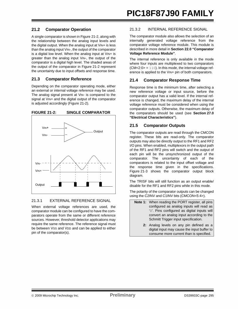
© 2009 Microchip Technology Inc. Preliminary DS39933C-page 295
PIC18F87J90 FAMILY21.2 Comparator OperationA single comparator is shown in Figure 21-2, along withthe relationship between the analog input levels andthe digital output. When the analog input at VIN+ is lessthan the analog input VIN-, the output of the comparatoris a digital low level. When the analog input at VIN+ isgreater than the analog input VIN-, the output of thecomparator is a digital high level. The shaded areas ofthe output of the comparator in Figure 21-2 representthe uncertainty due to input offsets and response time.
21.3 Comparator ReferenceDepending on the comparator operating mode, eitheran external or internal voltage reference may be used.The analog signal present at VIN- is compared to thesignal at VIN+ and the digital output of the comparatoris adjusted accordingly (Figure 21-2).
FIGURE 21-2: SINGLE COMPARATOR
21.3.1 EXTERNAL REFERENCE SIGNALWhen external voltage references are used, thecomparator module can be configured to have the com-parators operate from the same or different referencesources. However, threshold detector applications mayrequire the same reference. The reference signal mustbe between VSS and VDD and can be applied to eitherpin of the comparator(s).
21.3.2 INTERNAL REFERENCE SIGNAL
The comparator module also allows the selection of aninternally generated voltage reference from thecomparator voltage reference module. This module isdescribed in more detail in Section 22.0 “ComparatorVoltage Reference Module”.
The internal reference is only available in the modewhere four inputs are multiplexed to two comparators(CM<2:0> = 110). In this mode, the internal voltage ref-erence is applied to the VIN+ pin of both comparators.
21.4 Comparator Response TimeResponse time is the minimum time, after selecting anew reference voltage or input source, before thecomparator output has a valid level. If the internal ref-erence is changed, the maximum delay of the internalvoltage reference must be considered when using thecomparator outputs. Otherwise, the maximum delay ofthe comparators should be used (see Section 27.0“Electrical Characteristics”).
21.5 Comparator OutputsThe comparator outputs are read through the CMCONregister. These bits are read-only. The comparatoroutputs may also be directly output to the RF1 and RF2I/O pins. When enabled, multiplexors in the output pathof the RF1 and RF2 pins will switch and the output ofeach pin will be the unsynchronized output of thecomparator. The uncertainty of each of thecomparators is related to the input offset voltage andthe response time given in the specifications.Figure 21-3 shows the comparator output blockdiagram.
The TRISF bits will still function as an output enable/disable for the RF1 and RF2 pins while in this mode.
The polarity of the comparator outputs can be changedusing the C2INV and C1INV bits (CMCON<5:4>).
–
+VIN+
VIN-Output
Output
VIN-
VIN+
Note 1: When reading the PORT register, all pinsconfigured as analog inputs will read as‘0’. Pins configured as digital inputs willconvert an analog input according to theSchmitt Trigger input specification.
2: Analog levels on any pin defined as adigital input may cause the input buffer toconsume more current than is specified.
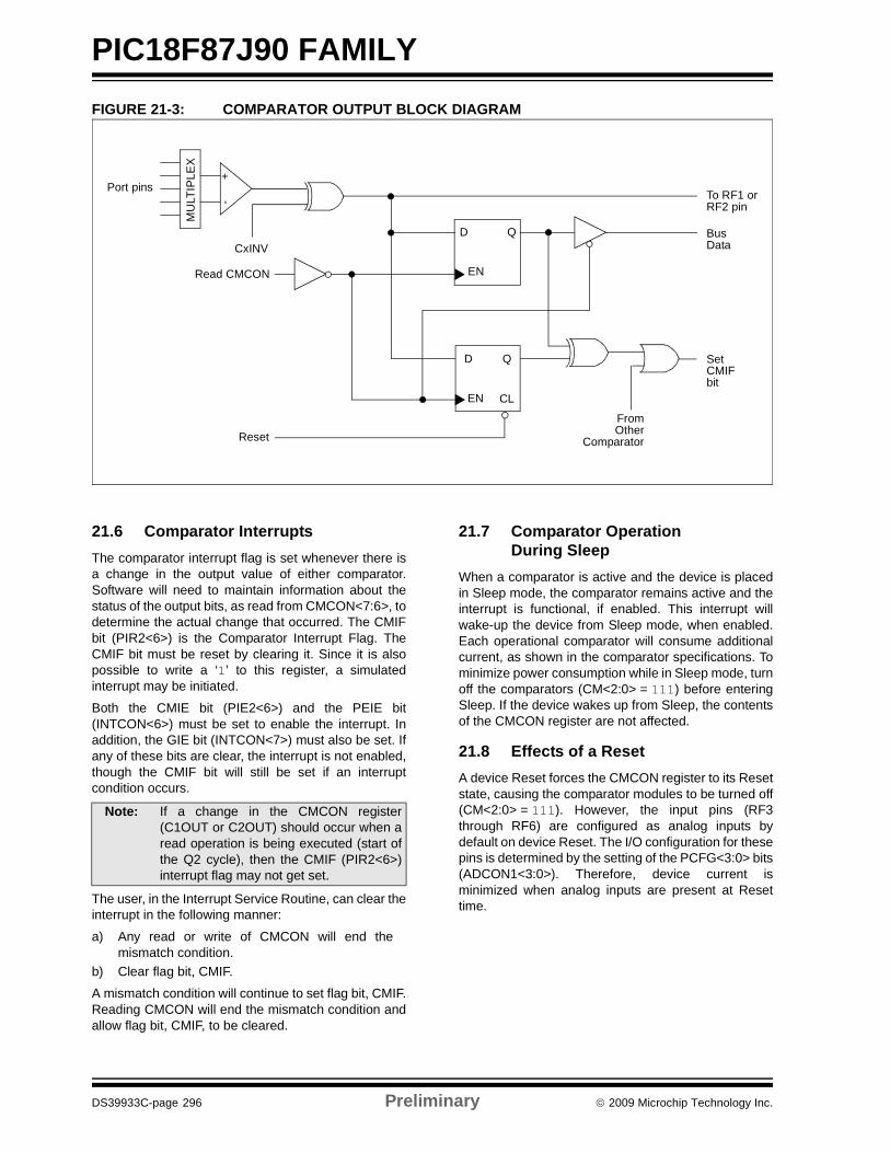
PIC18F87J90 FAMILY
DS39933C-page 296 Preliminary © 2009 Microchip Technology Inc.
FIGURE 21-3: COMPARATOR OUTPUT BLOCK DIAGRAM
21.6 Comparator InterruptsThe comparator interrupt flag is set whenever there isa change in the output value of either comparator.Software will need to maintain information about thestatus of the output bits, as read from CMCON<7:6>, todetermine the actual change that occurred. The CMIFbit (PIR2<6>) is the Comparator Interrupt Flag. TheCMIF bit must be reset by clearing it. Since it is alsopossible to write a ‘1’ to this register, a simulatedinterrupt may be initiated.
Both the CMIE bit (PIE2<6>) and the PEIE bit(INTCON<6>) must be set to enable the interrupt. Inaddition, the GIE bit (INTCON<7>) must also be set. Ifany of these bits are clear, the interrupt is not enabled,though the CMIF bit will still be set if an interruptcondition occurs.
The user, in the Interrupt Service Routine, can clear theinterrupt in the following manner:
a) Any read or write of CMCON will end themismatch condition.
b) Clear flag bit, CMIF.
A mismatch condition will continue to set flag bit, CMIF.Reading CMCON will end the mismatch condition andallow flag bit, CMIF, to be cleared.
21.7 Comparator Operation During Sleep
When a comparator is active and the device is placedin Sleep mode, the comparator remains active and theinterrupt is functional, if enabled. This interrupt willwake-up the device from Sleep mode, when enabled.Each operational comparator will consume additionalcurrent, as shown in the comparator specifications. Tominimize power consumption while in Sleep mode, turnoff the comparators (CM<2:0> = 111) before enteringSleep. If the device wakes up from Sleep, the contentsof the CMCON register are not affected.
21.8 Effects of a ResetA device Reset forces the CMCON register to its Resetstate, causing the comparator modules to be turned off(CM<2:0> = 111). However, the input pins (RF3through RF6) are configured as analog inputs bydefault on device Reset. The I/O configuration for thesepins is determined by the setting of the PCFG<3:0> bits(ADCON1<3:0>). Therefore, device current isminimized when analog inputs are present at Resettime.
D Q
EN
To RF1 orRF2 pin
BusData
Set
MU
LTIP
LEX
CMIFbit
-+
Port pins
Read CMCON
ResetFromOther
Comparator
CxINV
D Q
EN CL
Note: If a change in the CMCON register(C1OUT or C2OUT) should occur when aread operation is being executed (start ofthe Q2 cycle), then the CMIF (PIR2<6>)interrupt flag may not get set.
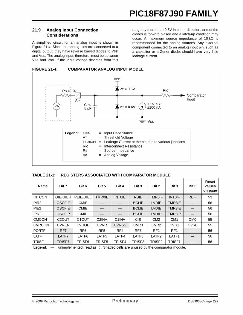
© 2009 Microchip Technology Inc. Preliminary DS39933C-page 297
PIC18F87J90 FAMILY21.9 Analog Input Connection
ConsiderationsA simplified circuit for an analog input is shown inFigure 21-4. Since the analog pins are connected to adigital output, they have reverse biased diodes to VDDand VSS. The analog input, therefore, must be betweenVSS and VDD. If the input voltage deviates from this
range by more than 0.6V in either direction, one of thediodes is forward biased and a latch-up condition mayoccur. A maximum source impedance of 10 kΩ isrecommended for the analog sources. Any externalcomponent connected to an analog input pin, such asa capacitor or a Zener diode, should have very littleleakage current.
FIGURE 21-4: COMPARATOR ANALOG INPUT MODEL
TABLE 21-1: REGISTERS ASSOCIATED WITH COMPARATOR MODULE
Name Bit 7 Bit 6 Bit 5 Bit 4 Bit 3 Bit 2 Bit 1 Bit 0Reset Values
on page
INTCON GIE/GIEH PEIE/GIEL TMR0IE INT0IE RBIE TMR0IF INT0IF RBIF 53PIR2 OSCFIF CMIF — — BCLIF LVDIF TMR3IF — 56PIE2 OSCFIE CMIE — — BCLIE LVDIE TMR3IE — 56IPR2 OSCFIP CMIP — — BCLIP LVDIP TMR3IP — 56CMCON C2OUT C1OUT C2INV C1INV CIS CM2 CM1 CM0 55CVRCON CVREN CVROE CVRR CVRSS CVR3 CVR2 CVR1 CVR0 55PORTF RF7 RF6 RF5 RF4 RF3 RF2 RF1 — 56LATF LATF7 LATF6 LATF5 LATF4 LATF3 LATF2 LATF1 — 56TRISF TRISF7 TRISF6 TRISF5 TRISF4 TRISF3 TRISF2 TRISF1 — 56Legend: — = unimplemented, read as ‘0’. Shaded cells are unused by the comparator module.
VA
RS < 10k
AINCPIN5 pF
VDD
VT = 0.6V
VT = 0.6V
RIC
ILEAKAGE±100 nA
VSS
Legend: CPIN = Input CapacitanceVT = Threshold VoltageILEAKAGE = Leakage Current at the pin due to various junctionsRIC = Interconnect ResistanceRS = Source ImpedanceVA = Analog Voltage
ComparatorInput

PIC18F87J90 FAMILY
DS39933C-page 298 Preliminary © 2009 Microchip Technology Inc.
NOTES:
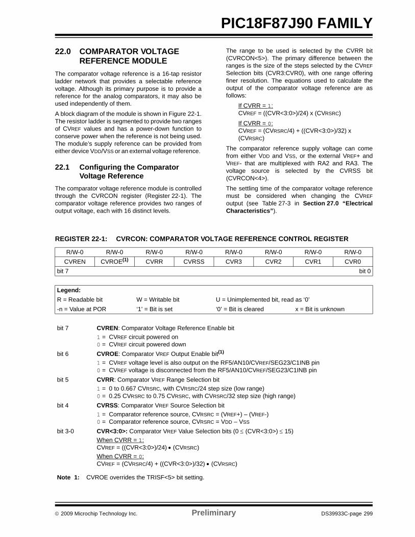
© 2009 Microchip Technology Inc. Preliminary DS39933C-page 299
PIC18F87J90 FAMILY
22.0 COMPARATOR VOLTAGE REFERENCE MODULE
The comparator voltage reference is a 16-tap resistorladder network that provides a selectable referencevoltage. Although its primary purpose is to provide areference for the analog comparators, it may also beused independently of them.
A block diagram of the module is shown in Figure 22-1.The resistor ladder is segmented to provide two rangesof CVREF values and has a power-down function toconserve power when the reference is not being used.The module’s supply reference can be provided fromeither device VDD/VSS or an external voltage reference.
22.1 Configuring the Comparator Voltage Reference
The comparator voltage reference module is controlledthrough the CVRCON register (Register 22-1). Thecomparator voltage reference provides two ranges ofoutput voltage, each with 16 distinct levels.
The range to be used is selected by the CVRR bit(CVRCON<5>). The primary difference between theranges is the size of the steps selected by the CVREFSelection bits (CVR3:CVR0), with one range offeringfiner resolution. The equations used to calculate theoutput of the comparator voltage reference are asfollows:
If CVRR = 1: CVREF = ((CVR<3:0>)/24) x (CVRSRC)
If CVRR = 0: CVREF = (CVRSRC/4) + ((CVR<3:0>)/32) x(CVRSRC)
The comparator reference supply voltage can comefrom either VDD and VSS, or the external VREF+ andVREF- that are multiplexed with RA2 and RA3. Thevoltage source is selected by the CVRSS bit(CVRCON<4>).
The settling time of the comparator voltage referencemust be considered when changing the CVREFoutput (see Table 27-3 in Section 27.0 “ElectricalCharacteristics”).
REGISTER 22-1: CVRCON: COMPARATOR VOLTAGE REFERENCE CONTROL REGISTER
R/W-0 R/W-0 R/W-0 R/W-0 R/W-0 R/W-0 R/W-0 R/W-0CVREN CVROE(1) CVRR CVRSS CVR3 CVR2 CVR1 CVR0
bit 7 bit 0
Legend:R = Readable bit W = Writable bit U = Unimplemented bit, read as ‘0’-n = Value at POR ‘1’ = Bit is set ‘0’ = Bit is cleared x = Bit is unknown
bit 7 CVREN: Comparator Voltage Reference Enable bit1 = CVREF circuit powered on 0 = CVREF circuit powered down
bit 6 CVROE: Comparator VREF Output Enable bit(1)
1 = CVREF voltage level is also output on the RF5/AN10/CVREF/SEG23/C1INB pin 0 = CVREF voltage is disconnected from the RF5/AN10/CVREF/SEG23/C1INB pin
bit 5 CVRR: Comparator VREF Range Selection bit1 = 0 to 0.667 CVRSRC, with CVRSRC/24 step size (low range)0 = 0.25 CVRSRC to 0.75 CVRSRC, with CVRSRC/32 step size (high range)
bit 4 CVRSS: Comparator VREF Source Selection bit1 = Comparator reference source, CVRSRC = (VREF+) – (VREF-)0 = Comparator reference source, CVRSRC = VDD – VSS
bit 3-0 CVR<3:0>: Comparator VREF Value Selection bits (0 ≤ (CVR<3:0>) ≤ 15) When CVRR = 1: CVREF = ((CVR<3:0>)/24) • (CVRSRC)When CVRR = 0: CVREF = (CVRSRC/4) + ((CVR<3:0>)/32) • (CVRSRC)
Note 1: CVROE overrides the TRISF<5> bit setting.
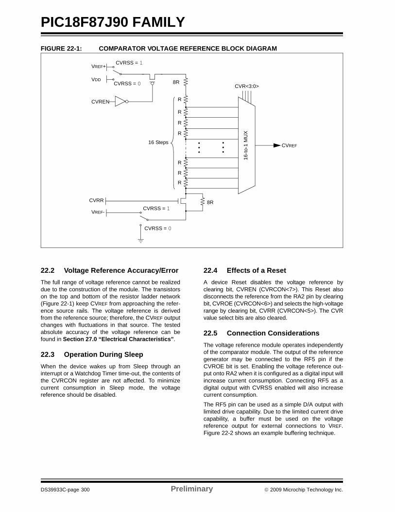
PIC18F87J90 FAMILY
DS39933C-page 300 Preliminary © 2009 Microchip Technology Inc.
FIGURE 22-1: COMPARATOR VOLTAGE REFERENCE BLOCK DIAGRAM
22.2 Voltage Reference Accuracy/ErrorThe full range of voltage reference cannot be realizeddue to the construction of the module. The transistorson the top and bottom of the resistor ladder network(Figure 22-1) keep CVREF from approaching the refer-ence source rails. The voltage reference is derivedfrom the reference source; therefore, the CVREF outputchanges with fluctuations in that source. The testedabsolute accuracy of the voltage reference can befound in Section 27.0 “Electrical Characteristics”.
22.3 Operation During SleepWhen the device wakes up from Sleep through aninterrupt or a Watchdog Timer time-out, the contents ofthe CVRCON register are not affected. To minimizecurrent consumption in Sleep mode, the voltagereference should be disabled.
22.4 Effects of a ResetA device Reset disables the voltage reference byclearing bit, CVREN (CVRCON<7>). This Reset alsodisconnects the reference from the RA2 pin by clearingbit, CVROE (CVRCON<6>) and selects the high-voltagerange by clearing bit, CVRR (CVRCON<5>). The CVRvalue select bits are also cleared.
22.5 Connection ConsiderationsThe voltage reference module operates independentlyof the comparator module. The output of the referencegenerator may be connected to the RF5 pin if theCVROE bit is set. Enabling the voltage reference out-put onto RA2 when it is configured as a digital input willincrease current consumption. Connecting RF5 as adigital output with CVRSS enabled will also increasecurrent consumption.
The RF5 pin can be used as a simple D/A output withlimited drive capability. Due to the limited current drivecapability, a buffer must be used on the voltagereference output for external connections to VREF.Figure 22-2 shows an example buffering technique.
16-to
-1 M
UX
CVR<3:0>8R
RCVREN
CVRSS = 0VDD
VREF+CVRSS = 1
8R
CVRSS = 0
VREF-CVRSS = 1
R
R
R
R
R
R
16 Steps
CVRR
CVREF
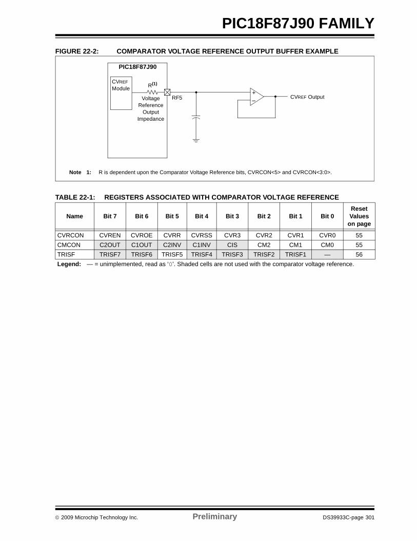
© 2009 Microchip Technology Inc. Preliminary DS39933C-page 301
PIC18F87J90 FAMILYFIGURE 22-2: COMPARATOR VOLTAGE REFERENCE OUTPUT BUFFER EXAMPLE
TABLE 22-1: REGISTERS ASSOCIATED WITH COMPARATOR VOLTAGE REFERENCE
Name Bit 7 Bit 6 Bit 5 Bit 4 Bit 3 Bit 2 Bit 1 Bit 0Reset Values
on page
CVRCON CVREN CVROE CVRR CVRSS CVR3 CVR2 CVR1 CVR0 55CMCON C2OUT C1OUT C2INV C1INV CIS CM2 CM1 CM0 55TRISF TRISF7 TRISF6 TRISF5 TRISF4 TRISF3 TRISF2 TRISF1 — 56Legend: — = unimplemented, read as ‘0’. Shaded cells are not used with the comparator voltage reference.
CVREF Output+–
CVREFModule
Voltage Reference
Output Impedance
R(1)
RF5
Note 1: R is dependent upon the Comparator Voltage Reference bits, CVRCON<5> and CVRCON<3:0>.
PIC18F87J90

PIC18F87J90 FAMILY
DS39933C-page 302 Preliminary © 2009 Microchip Technology Inc.
NOTES:
© 2009 Microchip Technology Inc. Preliminary DS39933C-page 303
PIC18F87J90 FAMILY
23.0 CHARGE TIME MEASUREMENT UNIT (CTMU)
The Charge Time Measurement Unit (CTMU) is aflexible analog module that provides accurate differen-tial time measurement between pulse sources, as wellas asynchronous pulse generation. By working withother on-chip analog modules, the CTMU can be usedto precisely measure time, measure capacitance,measure relative changes in capacitance or generateoutput pulses with a specific time delay. The CTMU isideal for interfacing with capacitive-based sensors.
The module includes the following key features:
• Up to 13 channels available for capacitive or time measurement input
• On-chip precision current source• Four-edge input trigger sources• Polarity control for each edge source
• Control of edge sequence• Control of response to edges• Time measurement resolution of 1 nanosecond• High precision time measurement• Time delay of external or internal signal
asynchronous to system clock• Accurate current source suitable for capacitive
measurement
The CTMU works in conjunction with the A/D Converterto provide up to 13 channels for time or chargemeasurement, depending on the specific device andthe number of A/D channels available. When config-ured for time delay, the CTMU is connected to one ofthe analog comparators. The level-sensitive input edgesources can be selected from four sources: twoexternal inputs or CCP1/CCP2 Special Event Triggers.
Figure 23-1 provides a block diagram of the CTMU.
FIGURE 23-1: CTMU BLOCK DIAGRAM
CTEDG1
CTEDG2
Current Source
EdgeControlLogic
CTMUCON
PulseGenerator
A/D Converter Comparator 2Input
CCP2
CCP1
CurrentControl
ITRIM<5:0>IRNG<1:0>
CTMUICON
CTMUControlLogic
EDGENEDGSEQENEDG1SELxEDG1POLEDG2SELxEDG2POL
EDG1STATEDG2STAT
TGENIDISSENCTTRIG
A/D Trigger
CTPLS
Comparator 2 Output
PIC18F87J90 FAMILY
DS39933C-page 304 Preliminary © 2009 Microchip Technology Inc.
23.1 CTMU OperationThe CTMU works by using a fixed current source tocharge a circuit. The type of circuit depends on the typeof measurement being made. In the case of chargemeasurement, the current is fixed, and the amount oftime the current is applied to the circuit is fixed. Theamount of voltage read by the A/D is then a measure-ment of the capacitance of the circuit. In the case oftime measurement, the current, as well as the capaci-tance of the circuit, is fixed. In this case, the voltageread by the A/D is then representative of the amount oftime elapsed from the time the current source startsand stops charging the circuit.
If the CTMU is being used as a time delay, both capaci-tance and current source are fixed, as well as the voltagesupplied to the comparator circuit. The delay of a signalis determined by the amount of time it takes the voltageto charge to the comparator threshold voltage.
23.1.1 THEORY OF OPERATIONThe operation of the CTMU is based on the equationfor charge:
More simply, the amount of charge measured incoulombs in a circuit is defined as current in amperes(I) multiplied by the amount of time in seconds that thecurrent flows (t). Charge is also defined as the capaci-tance in farads (C) multiplied by the voltage of thecircuit (V). It follows that:
The CTMU module provides a constant, known currentsource. The A/D Converter is used to measure (V) inthe equation, leaving two unknowns: capacitance (C)and time (t). The above equation can be used to calcu-late capacitance or time, by either the relationshipusing the known fixed capacitance of the circuit:
or by:
using a fixed time that the current source is applied tothe circuit.
23.1.2 CURRENT SOURCEAt the heart of the CTMU is a precision current source,designed to provide a constant reference for measure-ments. The level of current is user-selectable acrossthree ranges or a total of two orders of magnitude, withthe ability to trim the output in ±2% increments(nominal). The current range is selected by theIRNG<1:0> bits (CTMUICON<9:8>), with a value of‘00’ representing the lowest range.
Current trim is provided by the ITRIM<5:0> bits(CTMUICON<7:2>). These six bits allow trimming ofthe current source in steps of approximately 2% perstep. Note that half of the range adjusts the currentsource positively and the other half reduces the currentsource. A value of ‘000000’ is the neutral position (nochange). A value of ‘100000’ is the maximum negativeadjustment (approximately -62%), and ‘011111’ is themaximum positive adjustment (approximately +62%).
23.1.3 EDGE SELECTION AND CONTROLCTMU measurements are controlled by edge eventsoccurring on the module’s two input channels. Eachchannel, referred to as Edge 1 and Edge 2, can be con-figured to receive input pulses from one of the edgeinput pins (CTEDG1 and CTEDG2) or CCPx SpecialEvent Triggers. The input channels are level-sensitive,responding to the instantaneous level on the channelrather than a transition between levels. The inputs areselected using the EDG1SEL and EDG2SEL bit pairs(CTMUCONL<3:2, 6:5>).
In addition to source, each channel can be configured forevent polarity using the EDGE2POL and EDGE1POLbits (CTMUCONL<7,4>). The input channels can alsobe filtered for an edge event sequence (Edge 1 occur-ring before Edge 2) by setting the EDGSEQEN bit(CTMUCONH<2>).
23.1.4 EDGE STATUSThe CTMUCON register also contains two status bits,EDG2STAT and EDG1STAT (CTMUCONL<1:0>).Their primary function is to show if an edge responsehas occurred on the corresponding channel. TheCTMU automatically sets a particular bit when an edgeresponse is detected on its channel. The level-sensitivenature of the input channels also means that the statusbits become set immediately if the channel’s configura-tion is changed and is the same as the channel’scurrent state.
The module uses the edge status bits to control the cur-rent source output to external analog modules (such asthe A/D Converter). Current is only supplied to externalmodules when only one (but not both) of the status bitsis set, and shuts current off when both bits are eitherset or cleared. This allows the CTMU to measure cur-rent only during the interval between edges. After bothstatus bits are set, it is necessary to clear them beforeanother measurement is taken. Both bits should becleared simultaneously, if possible, to avoid re-enablingthe CTMU current source.
In addition to being set by the CTMU hardware, theedge status bits can also be set by software. This isalso the user’s application to manually enable or dis-able the current source. Setting either one (but notboth) of the bits enables the current source. Setting orclearing both bits at once disables the source.
C I dVdT-------⋅=
I t⋅ C V.⋅=
t C V⋅( ) I⁄=
C I t⋅( ) V⁄=
© 2009 Microchip Technology Inc. Preliminary DS39933C-page 305
PIC18F87J90 FAMILY23.1.5 INTERRUPTSThe CTMU sets its interrupt flag (PIR3<2>) wheneverthe current source is enabled, then disabled. An inter-rupt is generated only if the corresponding interruptenable bit (PIE3<2>) is also set. If edge sequencing isnot enabled (i.e., Edge 1 must occur before Edge 2), itis necessary to monitor the edge status bits anddetermine which edge occurred last and caused theinterrupt.
23.2 CTMU Module InitializationThe following sequence is a general guideline used toinitialize the CTMU module:
1. Select the current source range using the IRNGbits (CTMUICON<1:0>).
2. Adjust the current source trim using the ITRIMbits (CTMUICON<7:2>).
3. Configure the edge input sources for Edge 1 andEdge 2 by setting the EDG1SEL and EDG2SELbits (CTMUCONL<3:2 and 6:5>).
4. Configure the input polarities for the edge inputsusing the EDG1POL and EDG2POL bits(CTMUCONL<4,7>). The default configurationis for negative edge polarity (high-to-lowtransitions).
5. Enable edge sequencing using the EDGSEQENbit (CTMUCONH<2>). By default, edgesequencing is disabled.
6. Select the operating mode (Measurement orTime Delay) with the TGEN bit. The defaultmode is Time/Capacitance Measurement.
7. Configure the module to automatically triggeran A/D conversion when the second edgeevent has occurred using the CTTRIG bit(CTMUCONH<0>). The conversion trigger isdisabled by default.
8. Discharge the connected circuit by setting theIDISSEN bit (CTMUCONH<1>); after waiting asufficient time for the circuit to discharge, clearIDISSEN.
9. Disable the module by clearing the CTMUEN bit(CTMUCONH<7>).
10. Clear the Edge Status bits, EDG2STAT andEDG1STAT (CTMUCONL<1:0>).
11. Enable both edge inputs by setting the EDGENbit (CTMUCONH<3>).
12. Enable the module by setting the CTMUEN bit.
Depending on the type of measurement or pulsegeneration being performed, one or more additionalmodules may also need to be initialized and configuredwith the CTMU module:
• Edge Source Generation: In addition to the external edge input pins, CCPx Special Event Triggers can be used as edge sources for the CTMU.
• Capacitance or Time Measurement: The CTMU module uses the A/D Converter to measure the voltage across a capacitor that is connected to one of the analog input channels.
• Pulse Generation: When generating system clock independent output pulses, the CTMU module uses Comparator 2 and the associated comparator voltage reference.
23.3 Calibrating the CTMU ModuleThe CTMU requires calibration for precise measure-ments of capacitance and time, as well as for accuratetime delay. If the application only requires measurementof a relative change in capacitance or time, calibration isusually not necessary. An example of this type of appli-cation would include a capacitive touch switch, in whichthe touch circuit has a baseline capacitance, and theadded capacitance of the human body changes theoverall capacitance of a circuit.
If actual capacitance or time measurement is required,two hardware calibrations must take place: the currentsource needs calibration to set it to a precise current,and the circuit being measured needs calibration tomeasure and/or nullify all other capacitance other thanthat to be measured.
23.3.1 CURRENT SOURCE CALIBRATIONThe current source onboard the CTMU module has arange of ±60% nominal for each of three currentranges. Therefore, for precise measurements, it ispossible to measure and adjust this current source byplacing a high precision resistor, RCAL, onto an unusedanalog channel. An example circuit is shown inFigure 23-2. The current source measurement isperformed using the following steps:
1. Initialize the A/D Converter.2. Initialize the CTMU.3. Enable the current source by setting EDG1STAT
(CTMUCONL<0>).4. Issue settling time delay.5. Perform A/D conversion.6. Calculate the current source current using
I = V/RCAL, where RCAL is a high precisionresistance and V is measured by performing anA/D conversion.

PIC18F87J90 FAMILY
DS39933C-page 306 Preliminary © 2009 Microchip Technology Inc.
The CTMU current source may be trimmed with thetrim bits in CTMUICON using an iterative process to getan exact desired current. Alternatively, the nominalvalue without adjustment may be used; it may bestored by the software for use in all subsequentcapacitive or time measurements.
To calculate the value for RCAL, the nominal currentmust be chosen, and then the resistance can becalculated. For example, if the A/D Converter referencevoltage is 3.3V, use 70% of full scale, or 2.31V as thedesired approximate voltage to be read by the A/DConverter. If the range of the CTMU current source isselected to be 0.55 μA, the resistor value needed is cal-culated as RCAL = 2.31V/0.55 μA, for a value of 4.2 MΩ.Similarly, if the current source is chosen to be 5.5 μA,RCAL would be 420,000Ω, and 42,000Ω if the currentsource is set to 55 μA.
FIGURE 23-2: CTMU CURRENT SOURCE CALIBRATION CIRCUIT
A value of 70% of full-scale voltage is chosen to makesure that the A/D Converter was in a range that is wellabove the noise floor. Keep in mind that if an exact cur-rent is chosen to incorporate the trimming bits fromCTMUICON, the resistor value of RCAL may need to beadjusted accordingly. RCAL may be also adjusted toallow for available resistor values. RCAL should be ofthe highest precision available, keeping in mind theamount of precision needed for the circuit that theCTMU will be used to measure. A recommendedminimum would be 0.1% tolerance.
The following examples show one typical method forperforming a CTMU current calibration. Example 23-1demonstrates how to initialize the A/D Converter and theCTMU; this routine is typical for applications using bothmodules. Example 23-2 demonstrates one method forthe actual calibration routine. Note that this methodmanually triggers the A/D Converter; this is done todemonstrate the entire stepwise process. It is alsopossible to automatically trigger the conversion bysetting the CTMU’s CTTRIG bit (CTMUCONH<0>).
A/D Converter
CTMU
ANx
RCAL
Current Source
A/DTrigger
MUX
A/D
PIC18F87J90
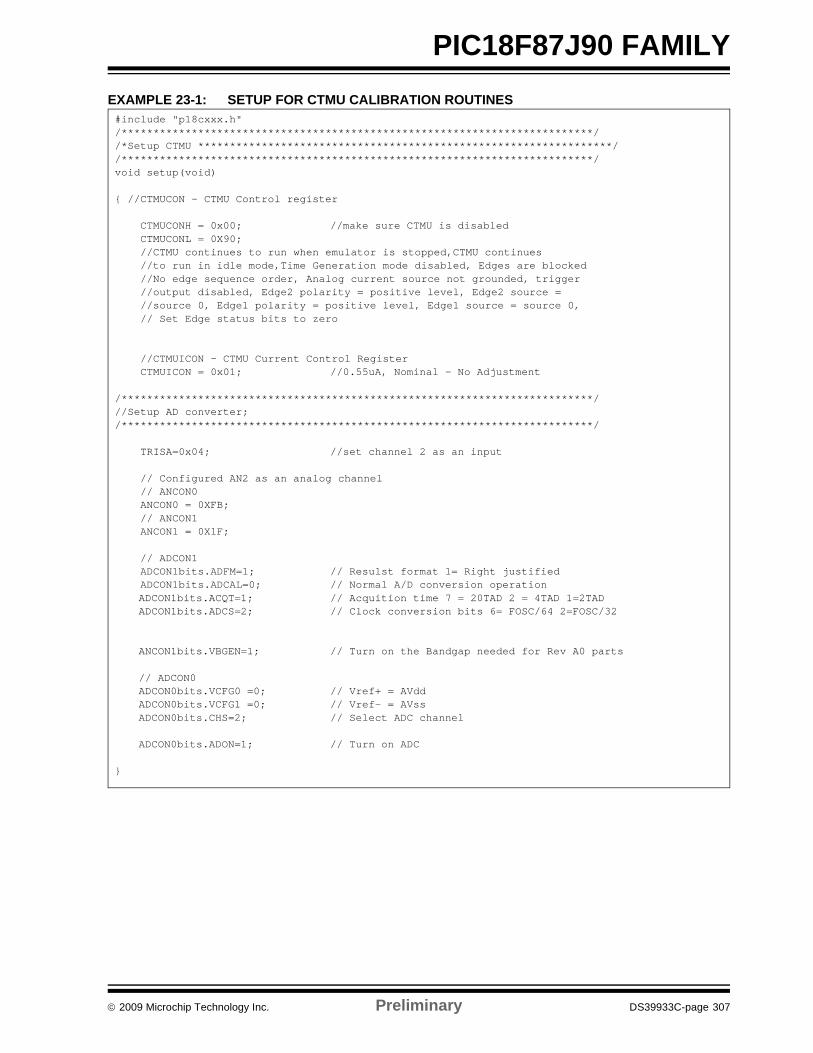
© 2009 Microchip Technology Inc. Preliminary DS39933C-page 307
PIC18F87J90 FAMILYEXAMPLE 23-1: SETUP FOR CTMU CALIBRATION ROUTINES#include "p18cxxx.h"/**************************************************************************//*Setup CTMU *****************************************************************//**************************************************************************/void setup(void)
//CTMUCON - CTMU Control register CTMUCONH = 0x00; //make sure CTMU is disabled CTMUCONL = 0X90; //CTMU continues to run when emulator is stopped,CTMU continues //to run in idle mode,Time Generation mode disabled, Edges are blocked //No edge sequence order, Analog current source not grounded, trigger //output disabled, Edge2 polarity = positive level, Edge2 source = //source 0, Edge1 polarity = positive level, Edge1 source = source 0, // Set Edge status bits to zero //CTMUICON - CTMU Current Control Register CTMUICON = 0x01; //0.55uA, Nominal - No Adjustment /**************************************************************************///Setup AD converter;/**************************************************************************/
TRISA=0x04; //set channel 2 as an input // Configured AN2 as an analog channel // ANCON0 ANCON0 = 0XFB; // ANCON1 ANCON1 = 0X1F; // ADCON1 ADCON1bits.ADFM=1; // Resulst format 1= Right justified ADCON1bits.ADCAL=0; // Normal A/D conversion operation
ADCON1bits.ACQT=1; // Acquition time 7 = 20TAD 2 = 4TAD 1=2TADADCON1bits.ADCS=2; // Clock conversion bits 6= FOSC/64 2=FOSC/32
ANCON1bits.VBGEN=1; // Turn on the Bandgap needed for Rev A0 parts
// ADCON0ADCON0bits.VCFG0 =0; // Vref+ = AVddADCON0bits.VCFG1 =0; // Vref- = AVssADCON0bits.CHS=2; // Select ADC channel
ADCON0bits.ADON=1; // Turn on ADC
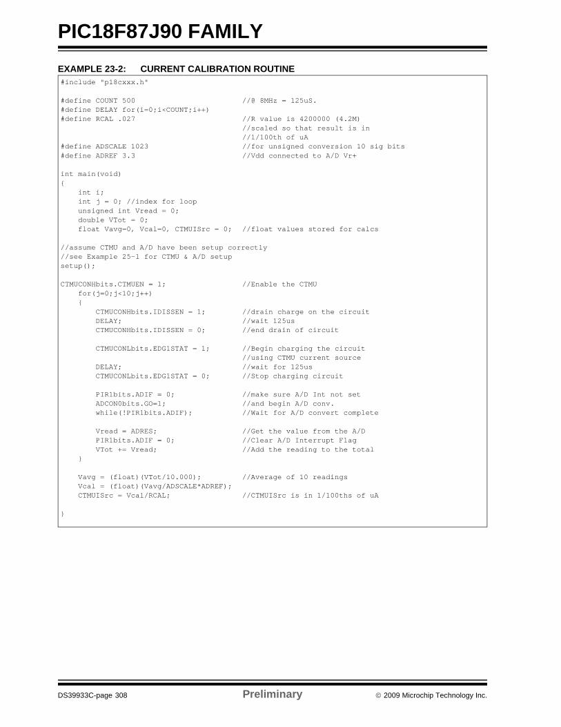
PIC18F87J90 FAMILY
DS39933C-page 308 Preliminary © 2009 Microchip Technology Inc.
EXAMPLE 23-2: CURRENT CALIBRATION ROUTINE#include "p18cxxx.h"
#define COUNT 500 //@ 8MHz = 125uS.#define DELAY for(i=0;i<COUNT;i++)#define RCAL .027 //R value is 4200000 (4.2M)
//scaled so that result is in//1/100th of uA
#define ADSCALE 1023 //for unsigned conversion 10 sig bits#define ADREF 3.3 //Vdd connected to A/D Vr+
int main(void) int i; int j = 0; //index for loop unsigned int Vread = 0; double VTot = 0; float Vavg=0, Vcal=0, CTMUISrc = 0; //float values stored for calcs
//assume CTMU and A/D have been setup correctly//see Example 25-1 for CTMU & A/D setupsetup();
CTMUCONHbits.CTMUEN = 1; //Enable the CTMU for(j=0;j<10;j++) CTMUCONHbits.IDISSEN = 1; //drain charge on the circuit DELAY; //wait 125us CTMUCONHbits.IDISSEN = 0; //end drain of circuit CTMUCONLbits.EDG1STAT = 1; //Begin charging the circuit
//using CTMU current source DELAY; //wait for 125us CTMUCONLbits.EDG1STAT = 0; //Stop charging circuit PIR1bits.ADIF = 0; //make sure A/D Int not set ADCON0bits.GO=1; //and begin A/D conv. while(!PIR1bits.ADIF); //Wait for A/D convert complete Vread = ADRES; //Get the value from the A/D PIR1bits.ADIF = 0; //Clear A/D Interrupt Flag VTot += Vread; //Add the reading to the total Vavg = (float)(VTot/10.000); //Average of 10 readings Vcal = (float)(Vavg/ADSCALE*ADREF); CTMUISrc = Vcal/RCAL; //CTMUISrc is in 1/100ths of uA
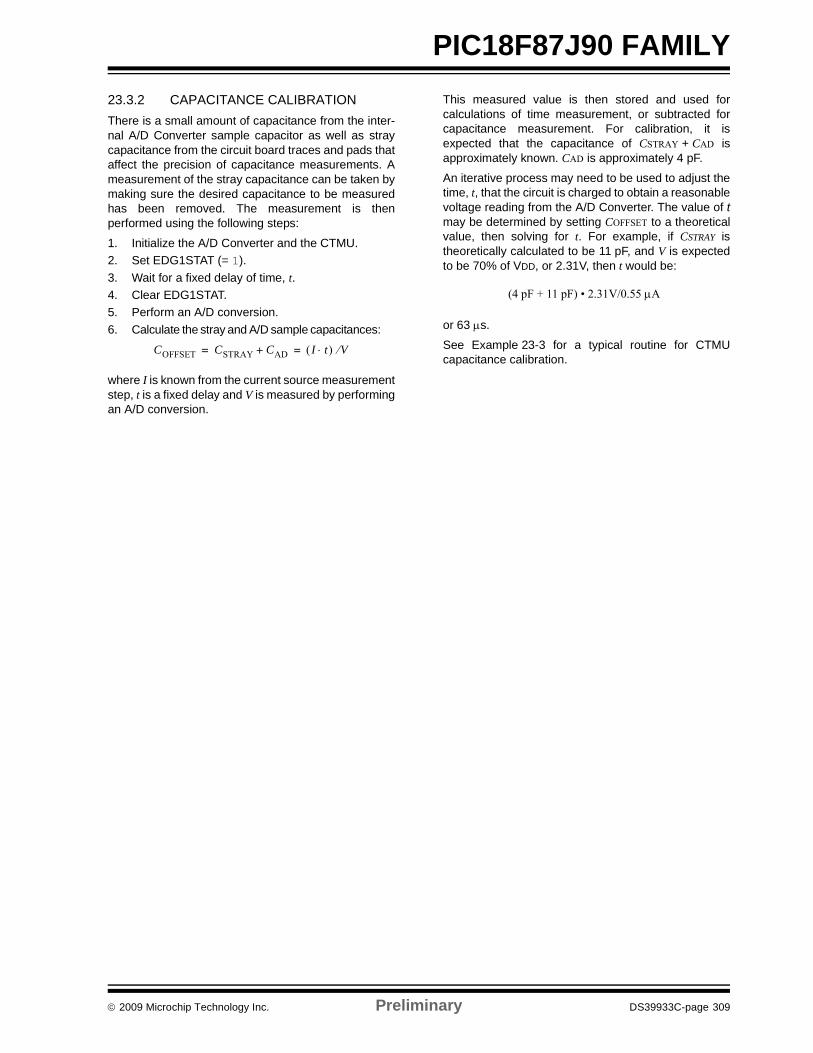
© 2009 Microchip Technology Inc. Preliminary DS39933C-page 309
PIC18F87J90 FAMILY23.3.2 CAPACITANCE CALIBRATIONThere is a small amount of capacitance from the inter-nal A/D Converter sample capacitor as well as straycapacitance from the circuit board traces and pads thataffect the precision of capacitance measurements. Ameasurement of the stray capacitance can be taken bymaking sure the desired capacitance to be measuredhas been removed. The measurement is thenperformed using the following steps:
1. Initialize the A/D Converter and the CTMU.2. Set EDG1STAT (= 1).3. Wait for a fixed delay of time, t.4. Clear EDG1STAT.5. Perform an A/D conversion.6. Calculate the stray and A/D sample capacitances:
where I is known from the current source measurementstep, t is a fixed delay and V is measured by performingan A/D conversion.
This measured value is then stored and used forcalculations of time measurement, or subtracted forcapacitance measurement. For calibration, it isexpected that the capacitance of CSTRAY + CAD isapproximately known. CAD is approximately 4 pF.
An iterative process may need to be used to adjust thetime, t, that the circuit is charged to obtain a reasonablevoltage reading from the A/D Converter. The value of tmay be determined by setting COFFSET to a theoreticalvalue, then solving for t. For example, if CSTRAY istheoretically calculated to be 11 pF, and V is expectedto be 70% of VDD, or 2.31V, then t would be:
or 63 μs.
See Example 23-3 for a typical routine for CTMUcapacitance calibration.
COFFSET CSTRAY CAD+ I t⋅( ) V⁄= =
(4 pF + 11 pF) • 2.31V/0.55 μA
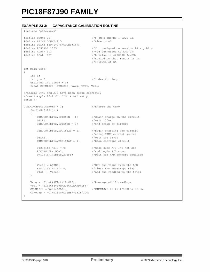
PIC18F87J90 FAMILY
DS39933C-page 310 Preliminary © 2009 Microchip Technology Inc.
EXAMPLE 23-3: CAPACITANCE CALIBRATION ROUTINE#include "p18cxxx.h"
#define COUNT 25 //@ 8MHz INTFRC = 62.5 us.#define ETIME COUNT*2.5 //time in uS#define DELAY for(i=0;i<COUNT;i++)#define ADSCALE 1023 //for unsigned conversion 10 sig bits#define ADREF 3.3 //Vdd connected to A/D Vr+#define RCAL .027 //R value is 4200000 (4.2M)
//scaled so that result is in//1/100th of uA
int main(void) int i; int j = 0; //index for loop unsigned int Vread = 0; float CTMUISrc, CTMUCap, Vavg, VTot, Vcal;
//assume CTMU and A/D have been setup correctly//see Example 25-1 for CTMU & A/D setupsetup();
CTMUCONHbits.CTMUEN = 1; //Enable the CTMU for(j=0;j<10;j++) CTMUCONHbits.IDISSEN = 1; //drain charge on the circuit DELAY; //wait 125us CTMUCONHbits.IDISSEN = 0; //end drain of circuit CTMUCONLbits.EDG1STAT = 1; //Begin charging the circuit
//using CTMU current source DELAY; //wait for 125us CTMUCONLbits.EDG1STAT = 0; //Stop charging circuit PIR1bits.ADIF = 0; //make sure A/D Int not set ADCON0bits.GO=1; //and begin A/D conv. while(!PIR1bits.ADIF); //Wait for A/D convert complete Vread = ADRES; //Get the value from the A/D PIR1bits.ADIF = 0; //Clear A/D Interrupt Flag VTot += Vread; //Add the reading to the total Vavg = (float)(VTot/10.000); //Average of 10 readings Vcal = (float)(Vavg/ADSCALE*ADREF); CTMUISrc = Vcal/RCAL; //CTMUISrc is in 1/100ths of uA CTMUCap = (CTMUISrc*ETIME/Vcal)/100;
© 2009 Microchip Technology Inc. Preliminary DS39933C-page 311
PIC18F87J90 FAMILY23.4 Measuring Capacitance with the
CTMUThere are two separate methods of measuring capaci-tance with the CTMU. The first is the absolute method,in which the actual capacitance value is desired. Thesecond is the relative method, in which the actualcapacitance is not needed, rather an indication of achange in capacitance is required.
23.4.1 ABSOLUTE CAPACITANCE MEASUREMENT
For absolute capacitance measurements, both thecurrent and capacitance calibration steps found inSection 23.3 “Calibrating the CTMU Module” shouldbe followed. Capacitance measurements are thenperformed using the following steps:
1. Initialize the A/D Converter.2. Initialize the CTMU.3. Set EDG1STAT.4. Wait for a fixed delay, T.5. Clear EDG1STAT.6. Perform an A/D conversion.7. Calculate the total capacitance, CTOTAL = (I * T)/V,
where I is known from the current sourcemeasurement step (Section 23.3.1 “CurrentSource Calibration”), T is a fixed delay and V ismeasured by performing an A/D conversion.
8. Subtract the stray and A/D capacitance(COFFSET from Section 23.3.2 “CapacitanceCalibration”) from CTOTAL to determine themeasured capacitance.
23.4.2 RELATIVE CHARGE MEASUREMENT
An application may not require precise capacitancemeasurements. For example, when detecting a validpress of a capacitance-based switch, detecting a relativechange of capacitance is of interest. In this type of appli-cation, when the switch is open (or not touched), the totalcapacitance is the capacitance of the combination of theboard traces, the A/D Converter, etc. A larger voltage willbe measured by the A/D Converter. When the switch isclosed (or is touched), the total capacitance is larger dueto the addition of the capacitance of the human body tothe above listed capacitances, and a smaller voltage willbe measured by the A/D Converter.
Detecting capacitance changes is easily accomplishedwith the CTMU using these steps:
1. Initialize the A/D Converter and the CTMU.2. Set EDG1STAT.3. Wait for a fixed delay.4. Clear EDG1STAT.5. Perform an A/D conversion.
The voltage measured by performing the A/D conver-sion is an indication of the relative capacitance. Notethat in this case, no calibration of the current source orcircuit capacitance measurement is needed. SeeExample 23-4 for a sample software routine for acapacitive touch switch.
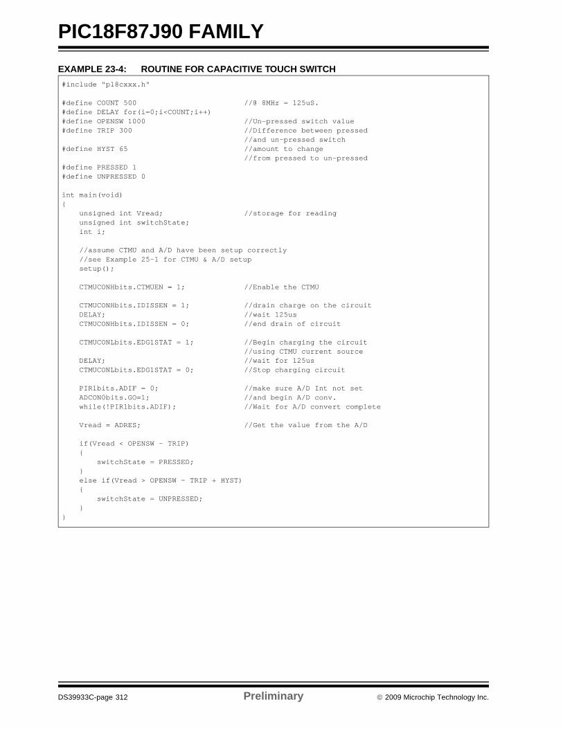
PIC18F87J90 FAMILY
DS39933C-page 312 Preliminary © 2009 Microchip Technology Inc.
EXAMPLE 23-4: ROUTINE FOR CAPACITIVE TOUCH SWITCH#include "p18cxxx.h"
#define COUNT 500 //@ 8MHz = 125uS.#define DELAY for(i=0;i<COUNT;i++)#define OPENSW 1000 //Un-pressed switch value#define TRIP 300 //Difference between pressed
//and un-pressed switch#define HYST 65 //amount to change
//from pressed to un-pressed#define PRESSED 1#define UNPRESSED 0
int main(void) unsigned int Vread; //storage for reading unsigned int switchState; int i; //assume CTMU and A/D have been setup correctly //see Example 25-1 for CTMU & A/D setup setup(); CTMUCONHbits.CTMUEN = 1; //Enable the CTMU CTMUCONHbits.IDISSEN = 1; //drain charge on the circuit DELAY; //wait 125us CTMUCONHbits.IDISSEN = 0; //end drain of circuit CTMUCONLbits.EDG1STAT = 1; //Begin charging the circuit //using CTMU current source DELAY; //wait for 125us CTMUCONLbits.EDG1STAT = 0; //Stop charging circuit PIR1bits.ADIF = 0; //make sure A/D Int not set ADCON0bits.GO=1; //and begin A/D conv. while(!PIR1bits.ADIF); //Wait for A/D convert complete Vread = ADRES; //Get the value from the A/D if(Vread < OPENSW - TRIP) switchState = PRESSED; else if(Vread > OPENSW - TRIP + HYST) switchState = UNPRESSED;
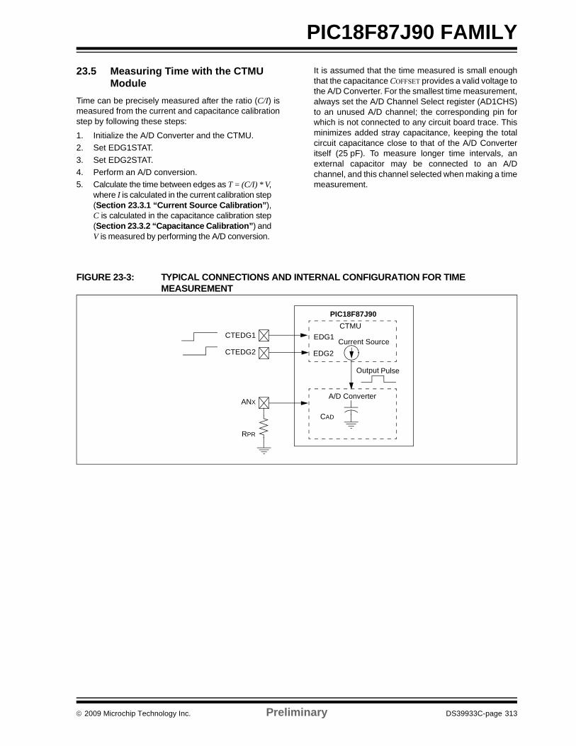
© 2009 Microchip Technology Inc. Preliminary DS39933C-page 313
PIC18F87J90 FAMILY23.5 Measuring Time with the CTMU
ModuleTime can be precisely measured after the ratio (C/I) ismeasured from the current and capacitance calibrationstep by following these steps:
1. Initialize the A/D Converter and the CTMU.2. Set EDG1STAT.3. Set EDG2STAT.4. Perform an A/D conversion.5. Calculate the time between edges as T = (C/I) * V,
where I is calculated in the current calibration step(Section 23.3.1 “Current Source Calibration”),C is calculated in the capacitance calibration step(Section 23.3.2 “Capacitance Calibration”) andV is measured by performing the A/D conversion.
It is assumed that the time measured is small enoughthat the capacitance COFFSET provides a valid voltage tothe A/D Converter. For the smallest time measurement,always set the A/D Channel Select register (AD1CHS)to an unused A/D channel; the corresponding pin forwhich is not connected to any circuit board trace. Thisminimizes added stray capacitance, keeping the totalcircuit capacitance close to that of the A/D Converteritself (25 pF). To measure longer time intervals, anexternal capacitor may be connected to an A/Dchannel, and this channel selected when making a timemeasurement.
FIGURE 23-3: TYPICAL CONNECTIONS AND INTERNAL CONFIGURATION FOR TIME MEASUREMENT
A/D Converter
CTMUCTEDG1
CTEDG2
ANX
Output Pulse
EDG1
EDG2
CAD
RPR
Current Source
PIC18F87J90
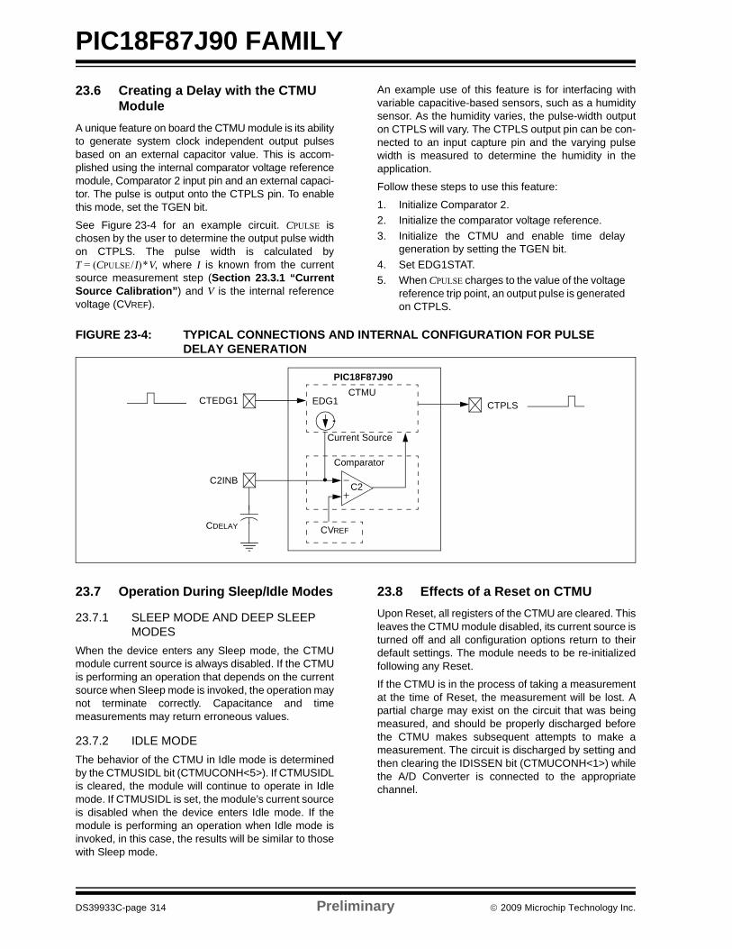
PIC18F87J90 FAMILY
DS39933C-page 314 Preliminary © 2009 Microchip Technology Inc.
23.6 Creating a Delay with the CTMU Module
A unique feature on board the CTMU module is its abilityto generate system clock independent output pulsesbased on an external capacitor value. This is accom-plished using the internal comparator voltage referencemodule, Comparator 2 input pin and an external capaci-tor. The pulse is output onto the CTPLS pin. To enablethis mode, set the TGEN bit.
See Figure 23-4 for an example circuit. CPULSE ischosen by the user to determine the output pulse widthon CTPLS. The pulse width is calculated byT = (CPULSE/I)*V, where I is known from the currentsource measurement step (Section 23.3.1 “CurrentSource Calibration”) and V is the internal referencevoltage (CVREF).
An example use of this feature is for interfacing withvariable capacitive-based sensors, such as a humiditysensor. As the humidity varies, the pulse-width outputon CTPLS will vary. The CTPLS output pin can be con-nected to an input capture pin and the varying pulsewidth is measured to determine the humidity in theapplication.
Follow these steps to use this feature:
1. Initialize Comparator 2.2. Initialize the comparator voltage reference.3. Initialize the CTMU and enable time delay
generation by setting the TGEN bit.4. Set EDG1STAT.5. When CPULSE charges to the value of the voltage
reference trip point, an output pulse is generatedon CTPLS.
FIGURE 23-4: TYPICAL CONNECTIONS AND INTERNAL CONFIGURATION FOR PULSE DELAY GENERATION
23.7 Operation During Sleep/Idle Modes
23.7.1 SLEEP MODE AND DEEP SLEEP MODES
When the device enters any Sleep mode, the CTMUmodule current source is always disabled. If the CTMUis performing an operation that depends on the currentsource when Sleep mode is invoked, the operation maynot terminate correctly. Capacitance and timemeasurements may return erroneous values.
23.7.2 IDLE MODEThe behavior of the CTMU in Idle mode is determinedby the CTMUSIDL bit (CTMUCONH<5>). If CTMUSIDLis cleared, the module will continue to operate in Idlemode. If CTMUSIDL is set, the module’s current sourceis disabled when the device enters Idle mode. If themodule is performing an operation when Idle mode isinvoked, in this case, the results will be similar to thosewith Sleep mode.
23.8 Effects of a Reset on CTMUUpon Reset, all registers of the CTMU are cleared. Thisleaves the CTMU module disabled, its current source isturned off and all configuration options return to theirdefault settings. The module needs to be re-initializedfollowing any Reset.
If the CTMU is in the process of taking a measurementat the time of Reset, the measurement will be lost. Apartial charge may exist on the circuit that was beingmeasured, and should be properly discharged beforethe CTMU makes subsequent attempts to make ameasurement. The circuit is discharged by setting andthen clearing the IDISSEN bit (CTMUCONH<1>) whilethe A/D Converter is connected to the appropriatechannel.
C2
CVREF
CTPLS
Current Source
Comparator
CTMUCTEDG1
C2INB
CDELAY
EDG1
PIC18F87J90
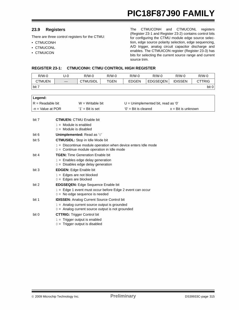
© 2009 Microchip Technology Inc. Preliminary DS39933C-page 315
PIC18F87J90 FAMILY23.9 RegistersThere are three control registers for the CTMU:
• CTMUCONH• CTMUCONL• CTMUICON
The CTMUCONH and CTMUCONL registers(Register 23-1 and Register 23-2) contains control bitsfor configuring the CTMU module edge source selec-tion, edge source polarity selection, edge sequencing,A/D trigger, analog circuit capacitor discharge andenables. The CTMUICON register (Register 23-3) hasbits for selecting the current source range and currentsource trim.
REGISTER 23-1: CTMUCONH: CTMU CONTROL HIGH REGISTER
R/W-0 U-0 R/W-0 R/W-0 R/W-0 R/W-0 R/W-0 R/W-0CTMUEN — CTMUSIDL TGEN EDGEN EDGSEQEN IDISSEN CTTRIG
bit 7 bit 0
Legend:R = Readable bit W = Writable bit U = Unimplemented bit, read as ‘0’-n = Value at POR ‘1’ = Bit is set ‘0’ = Bit is cleared x = Bit is unknown
bit 7 CTMUEN: CTMU Enable bit1 = Module is enabled0 = Module is disabled
bit 6 Unimplemented: Read as ‘0’bit 5 CTMUSIDL: Stop in Idle Mode bit
1 = Discontinue module operation when device enters Idle mode0 = Continue module operation in Idle mode
bit 4 TGEN: Time Generation Enable bit1 = Enables edge delay generation0 = Disables edge delay generation
bit 3 EDGEN: Edge Enable bit1 = Edges are not blocked0 = Edges are blocked
bit 2 EDGSEQEN: Edge Sequence Enable bit1 = Edge 1 event must occur before Edge 2 event can occur0 = No edge sequence is needed
bit 1 IDISSEN: Analog Current Source Control bit1 = Analog current source output is grounded0 = Analog current source output is not grounded
bit 0 CTTRIG: Trigger Control bit1 = Trigger output is enabled0 = Trigger output is disabled
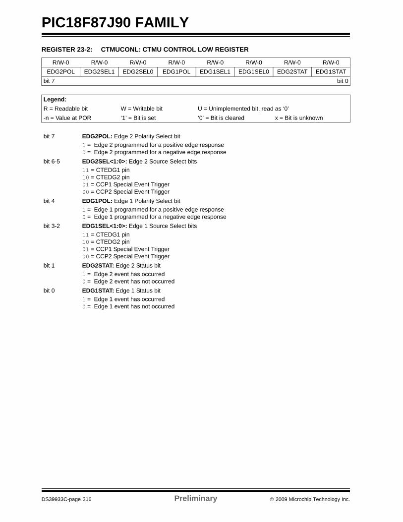
PIC18F87J90 FAMILY
DS39933C-page 316 Preliminary © 2009 Microchip Technology Inc.
REGISTER 23-2: CTMUCONL: CTMU CONTROL LOW REGISTER
R/W-0 R/W-0 R/W-0 R/W-0 R/W-0 R/W-0 R/W-0 R/W-0EDG2POL EDG2SEL1 EDG2SEL0 EDG1POL EDG1SEL1 EDG1SEL0 EDG2STAT EDG1STAT
bit 7 bit 0
Legend:R = Readable bit W = Writable bit U = Unimplemented bit, read as ‘0’-n = Value at POR ‘1’ = Bit is set ‘0’ = Bit is cleared x = Bit is unknown
bit 7 EDG2POL: Edge 2 Polarity Select bit1 = Edge 2 programmed for a positive edge response0 = Edge 2 programmed for a negative edge response
bit 6-5 EDG2SEL<1:0>: Edge 2 Source Select bits11 = CTEDG1 pin10 = CTEDG2 pin01 = CCP1 Special Event Trigger00 = CCP2 Special Event Trigger
bit 4 EDG1POL: Edge 1 Polarity Select bit1 = Edge 1 programmed for a positive edge response0 = Edge 1 programmed for a negative edge response
bit 3-2 EDG1SEL<1:0>: Edge 1 Source Select bits11 = CTEDG1 pin10 = CTEDG2 pin01 = CCP1 Special Event Trigger00 = CCP2 Special Event Trigger
bit 1 EDG2STAT: Edge 2 Status bit1 = Edge 2 event has occurred0 = Edge 2 event has not occurred
bit 0 EDG1STAT: Edge 1 Status bit1 = Edge 1 event has occurred0 = Edge 1 event has not occurred
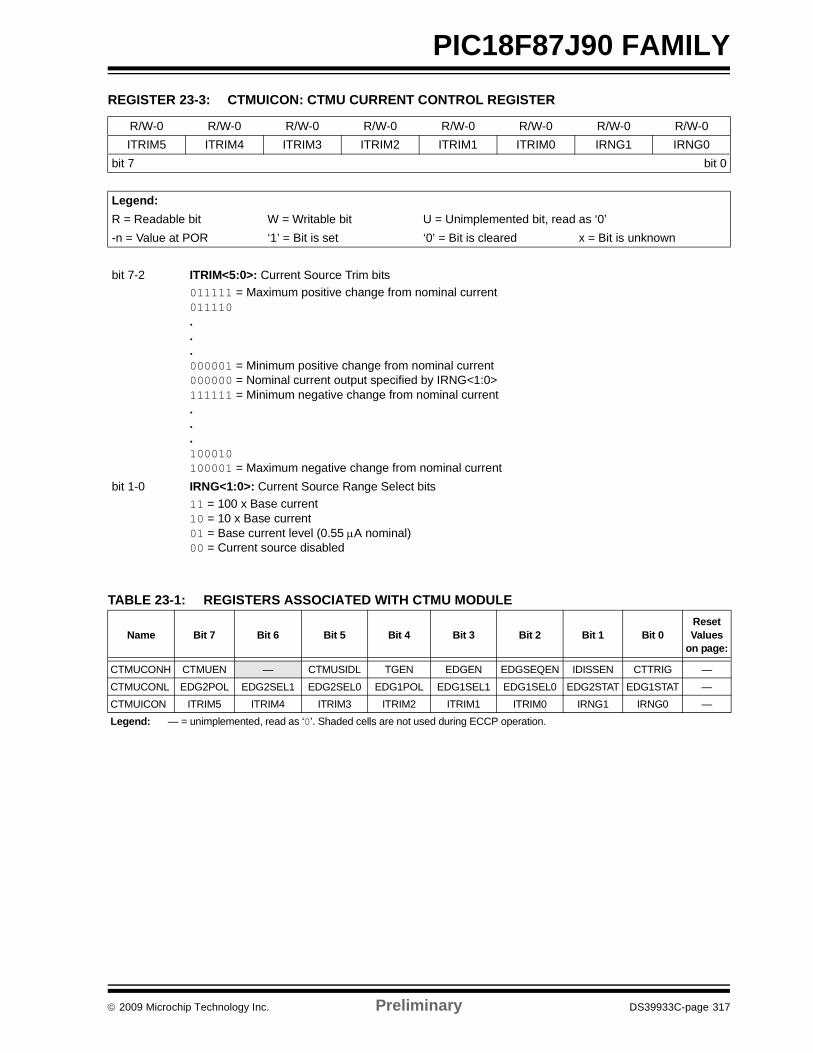
© 2009 Microchip Technology Inc. Preliminary DS39933C-page 317
PIC18F87J90 FAMILY
TABLE 23-1: REGISTERS ASSOCIATED WITH CTMU MODULE
REGISTER 23-3: CTMUICON: CTMU CURRENT CONTROL REGISTER
R/W-0 R/W-0 R/W-0 R/W-0 R/W-0 R/W-0 R/W-0 R/W-0ITRIM5 ITRIM4 ITRIM3 ITRIM2 ITRIM1 ITRIM0 IRNG1 IRNG0
bit 7 bit 0
Legend:R = Readable bit W = Writable bit U = Unimplemented bit, read as ‘0’-n = Value at POR ‘1’ = Bit is set ‘0’ = Bit is cleared x = Bit is unknown
bit 7-2 ITRIM<5:0>: Current Source Trim bits011111 = Maximum positive change from nominal current011110...000001 = Minimum positive change from nominal current000000 = Nominal current output specified by IRNG<1:0>111111 = Minimum negative change from nominal current...100010100001 = Maximum negative change from nominal current
bit 1-0 IRNG<1:0>: Current Source Range Select bits11 = 100 x Base current10 = 10 x Base current01 = Base current level (0.55 μA nominal)00 = Current source disabled
Name Bit 7 Bit 6 Bit 5 Bit 4 Bit 3 Bit 2 Bit 1 Bit 0Reset Values
on page:
CTMUCONH CTMUEN — CTMUSIDL TGEN EDGEN EDGSEQEN IDISSEN CTTRIG —CTMUCONL EDG2POL EDG2SEL1 EDG2SEL0 EDG1POL EDG1SEL1 EDG1SEL0 EDG2STAT EDG1STAT —CTMUICON ITRIM5 ITRIM4 ITRIM3 ITRIM2 ITRIM1 ITRIM0 IRNG1 IRNG0 —Legend: — = unimplemented, read as ‘0’. Shaded cells are not used during ECCP operation.

PIC18F87J90 FAMILY
DS39933C-page 318 Preliminary © 2009 Microchip Technology Inc.
NOTES:
© 2009 Microchip Technology Inc. Preliminary DS39933C-page 319
PIC18F87J90 FAMILY24.0 SPECIAL FEATURES OF THE
CPUPIC18F87J90 family devices include several featuresintended to maximize reliability and minimize costthrough elimination of external components. These are:• Oscillator Selection• Resets:
- Power-on Reset (POR)- Power-up Timer (PWRT)- Oscillator Start-up Timer (OST)- Brown-out Reset (BOR)
• Interrupts• Watchdog Timer (WDT)• Fail-Safe Clock Monitor• Two-Speed Start-up• Code Protection• In-Circuit Serial ProgrammingThe oscillator can be configured for the applicationdepending on frequency, power, accuracy and cost. Allof the options are discussed in detail in Section 2.0“Oscillator Configurations”.A complete discussion of device Resets and interruptsis available in previous sections of this data sheet.In addition to their Power-up and Oscillator Start-upTimers provided for Resets, the PIC18F87J90 familyfamily of devices have a configurable Watchdog Timerwhich is controlled in software.The inclusion of an internal RC oscillator also providesthe additional benefits of a Fail-Safe Clock Monitor(FSCM) and Two-Speed Start-up. FSCM provides forbackground monitoring of the peripheral clock andautomatic switchover in the event of its failure.Two-Speed Start-up enables code to be executedalmost immediately on start-up, while the primary clocksource completes its start-up delays. All of these features are enabled and configured bysetting the appropriate Configuration register bits.
24.1 Configuration BitsThe Configuration bits can be programmed (read as‘0’), or left unprogrammed (read as ‘1’), to selectvarious device configurations. These bits are mappedstarting at program memory location 300000h. Acomplete list is shown in Table 24-2. A detailedexplanation of the various bit functions is provided inRegister 24-1 through Register 24-6.
24.1.1 CONSIDERATIONS FOR CONFIGURING PIC18F87J90 FAMILY DEVICES
Devices of the PIC18F87J90 family do not use persis-tent memory registers to store configuration information.The configuration bytes are implemented as volatilememory which means that configuration data must beprogrammed each time the device is powered up.Configuration data is stored in the four words at the topof the on-chip program memory space, known as theFlash Configuration Words. It is stored in programmemory in the same order shown in Table 24-2, withCONFIG1L at the lowest address and CONFIG3H atthe highest. The data is automatically loaded in theproper Configuration registers during device power-up. When creating applications for these devices, usersshould always specifically allocate the location of theFlash Configuration Word for configuration data. This isto make certain that program code is not stored in thisaddress when the code is compiled.The volatile memory cells used for the Configurationbits always reset to ‘1’ on Power-on Resets. For allother types of Reset events, the previouslyprogrammed values are maintained and used withoutreloading from program memory. The four Most Significant bits of CONFIG1H,CONFIG2H and CONFIG3H in program memoryshould also be ‘1111’. This makes these ConfigurationWords appear to be NOP instructions in the remoteevent that their locations are ever executed byaccident. Since Configuration bits are not implementedin the corresponding locations, writing ‘1’s to theselocations has no effect on device operation. To prevent inadvertent configuration changes duringcode execution, all programmable Configuration bitsare write-once. After a bit is initially programmed duringa power cycle, it cannot be written to again. Changinga device configuration requires that power to the devicebe cycled.
TABLE 24-1: MAPPING OF THE FLASH CONFIGURATION WORDS TO THE CONFIGURATION REGISTERS
Configuration Byte
Code Space Address
Configuration RegisterAddress
CONFIG1L XXXF8h 300000hCONFIG1H XXXF9h 300001hCONFIG2L XXXFAh 300002hCONFIG2H XXXFBh 300003hCONFIG3L XXXFCh 300004hCONFIG3H XXXFDh 300005h
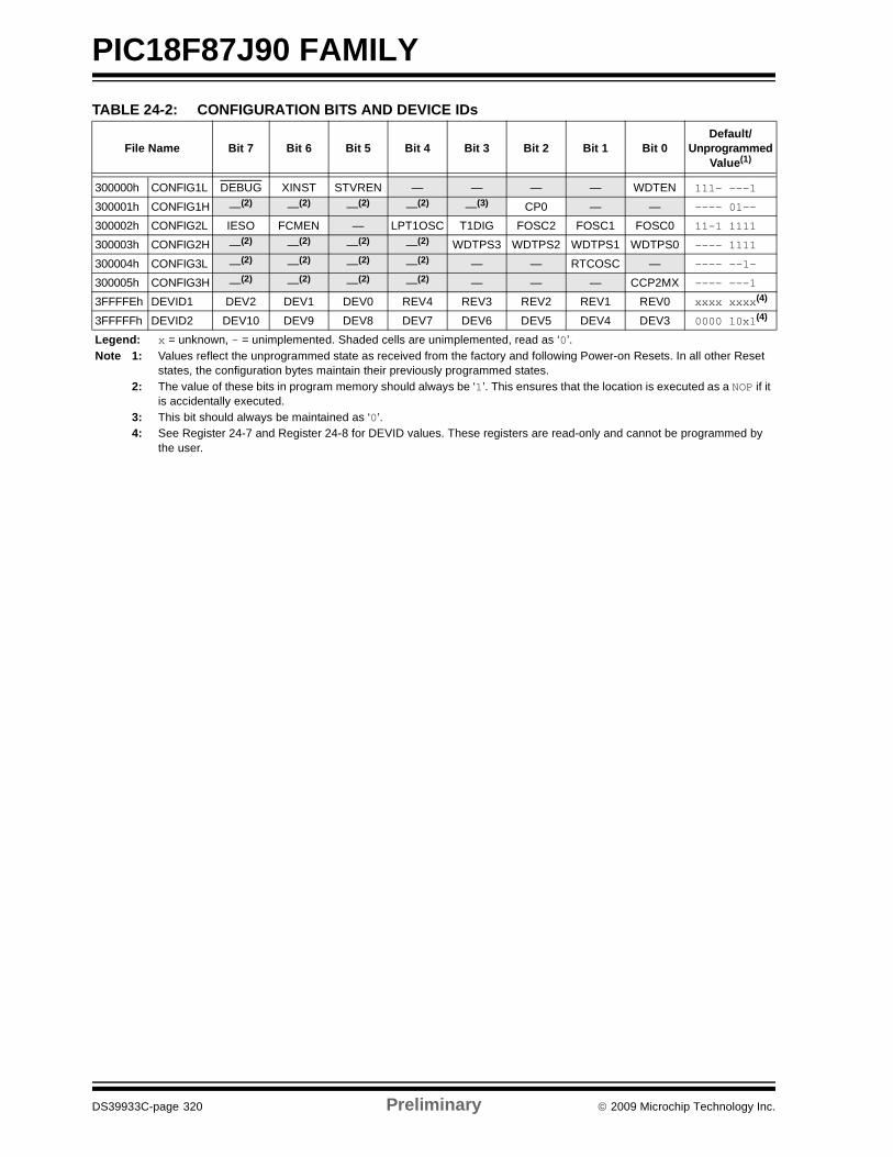
PIC18F87J90 FAMILY
DS39933C-page 320 Preliminary © 2009 Microchip Technology Inc.
TABLE 24-2: CONFIGURATION BITS AND DEVICE IDs
File Name Bit 7 Bit 6 Bit 5 Bit 4 Bit 3 Bit 2 Bit 1 Bit 0Default/
UnprogrammedValue(1)
300000h CONFIG1L DEBUG XINST STVREN — — — — WDTEN 111- ---1
300001h CONFIG1H —(2) —(2) —(2) —(2) —(3) CP0 — — ---- 01--
300002h CONFIG2L IESO FCMEN — LPT1OSC T1DIG FOSC2 FOSC1 FOSC0 11-1 1111
300003h CONFIG2H —(2) —(2) —(2) —(2) WDTPS3 WDTPS2 WDTPS1 WDTPS0 ---- 1111
300004h CONFIG3L —(2) —(2) —(2) —(2) — — RTCOSC — ---- --1-
300005h CONFIG3H —(2) —(2) —(2) —(2) — — — CCP2MX ---- ---1
3FFFFEh DEVID1 DEV2 DEV1 DEV0 REV4 REV3 REV2 REV1 REV0 xxxx xxxx(4)
3FFFFFh DEVID2 DEV10 DEV9 DEV8 DEV7 DEV6 DEV5 DEV4 DEV3 0000 10x1(4)
Legend: x = unknown, - = unimplemented. Shaded cells are unimplemented, read as ‘0’.Note 1: Values reflect the unprogrammed state as received from the factory and following Power-on Resets. In all other Reset
states, the configuration bytes maintain their previously programmed states.2: The value of these bits in program memory should always be ‘1’. This ensures that the location is executed as a NOP if it
is accidentally executed.3: This bit should always be maintained as ‘0’.4: See Register 24-7 and Register 24-8 for DEVID values. These registers are read-only and cannot be programmed by
the user.
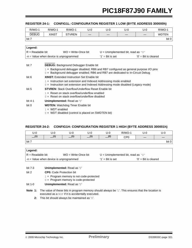
© 2009 Microchip Technology Inc. Preliminary DS39933C-page 321
PIC18F87J90 FAMILY
REGISTER 24-1: CONFIG1L: CONFIGURATION REGISTER 1 LOW (BYTE ADDRESS 300000h)
R/WO-1 R/WO-1 R/WO-1 U-0 U-0 U-0 U-0 R/WO-1
DEBUG XINST STVREN — — — — WDTENbit 7 bit 0
Legend:R = Readable bit WO = Write-Once bit U = Unimplemented bit, read as ‘0’-n = Value when device is unprogrammed ‘1’ = Bit is set ‘0’ = Bit is cleared
bit 7 DEBUG: Background Debugger Enable bit1 = Background debugger disabled; RB6 and RB7 configured as general purpose I/O pins0 = Background debugger enabled; RB6 and RB7 are dedicated to In-Circuit Debug
bit 6 XINST: Extended Instruction Set Enable bit1 = Instruction set extension and Indexed Addressing mode enabled0 = Instruction set extension and Indexed Addressing mode disabled (Legacy mode)
bit 5 STVREN: Stack Overflow/Underflow Reset Enable bit1 = Reset on stack overflow/underflow enabled 0 = Reset on stack overflow/underflow disabled
bit 4-1 Unimplemented: Read as ‘0’bit 0 WDTEN: Watchdog Timer Enable bit
1 = WDT enabled0 = WDT disabled (control is placed on SWDTEN bit)
REGISTER 24-2: CONFIG1H: CONFIGURATION REGISTER 1 HIGH (BYTE ADDRESS 300001h)
U-0 U-0 U-0 U-0 U-0 R/WO-1 U-0 U-0—(1) —(1) —(1) —(1) —(2) CP0 — —
bit 7 bit 0
Legend:R = Readable bit WO = Write-Once bit U = Unimplemented bit, read as ‘0’-n = Value when device is unprogrammed ‘1’ = Bit is set ‘0’ = Bit is cleared
bit 7-3 Unimplemented: Read as ‘0’bit 2 CP0: Code Protection bit
1 = Program memory is not code-protected0 = Program memory is code-protected
bit 1-0 Unimplemented: Read as ‘0’
Note 1: The value of these bits in program memory should always be ‘1’. This ensures that the location is executed as a NOP if it is accidentally executed.
2: This bit should always be maintained as ‘0’.
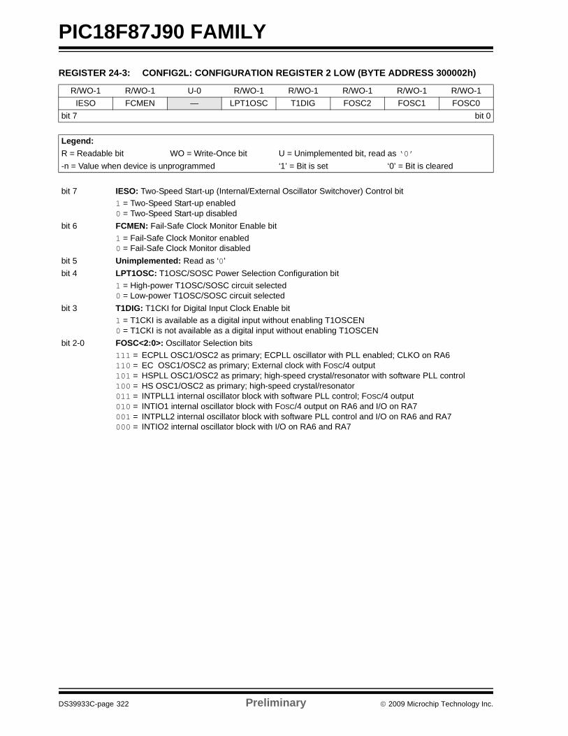
PIC18F87J90 FAMILY
DS39933C-page 322 Preliminary © 2009 Microchip Technology Inc.
REGISTER 24-3: CONFIG2L: CONFIGURATION REGISTER 2 LOW (BYTE ADDRESS 300002h)
R/WO-1 R/WO-1 U-0 R/WO-1 R/WO-1 R/WO-1 R/WO-1 R/WO-1IESO FCMEN — LPT1OSC T1DIG FOSC2 FOSC1 FOSC0
bit 7 bit 0
Legend:R = Readable bit WO = Write-Once bit U = Unimplemented bit, read as ‘0’-n = Value when device is unprogrammed ‘1’ = Bit is set ‘0’ = Bit is cleared
bit 7 IESO: Two-Speed Start-up (Internal/External Oscillator Switchover) Control bit1 = Two-Speed Start-up enabled0 = Two-Speed Start-up disabled
bit 6 FCMEN: Fail-Safe Clock Monitor Enable bit1 = Fail-Safe Clock Monitor enabled0 = Fail-Safe Clock Monitor disabled
bit 5 Unimplemented: Read as ‘0’bit 4 LPT1OSC: T1OSC/SOSC Power Selection Configuration bit
1 = High-power T1OSC/SOSC circuit selected0 = Low-power T1OSC/SOSC circuit selected
bit 3 T1DIG: T1CKI for Digital Input Clock Enable bit1 = T1CKI is available as a digital input without enabling T1OSCEN0 = T1CKI is not available as a digital input without enabling T1OSCEN
bit 2-0 FOSC<2:0>: Oscillator Selection bits111 = ECPLL OSC1/OSC2 as primary; ECPLL oscillator with PLL enabled; CLKO on RA6110 = EC OSC1/OSC2 as primary; External clock with FOSC/4 output101 = HSPLL OSC1/OSC2 as primary; high-speed crystal/resonator with software PLL control100 = HS OSC1/OSC2 as primary; high-speed crystal/resonator011 = INTPLL1 internal oscillator block with software PLL control; FOSC/4 output010 = INTIO1 internal oscillator block with FOSC/4 output on RA6 and I/O on RA7001 = INTPLL2 internal oscillator block with software PLL control and I/O on RA6 and RA7000 = INTIO2 internal oscillator block with I/O on RA6 and RA7
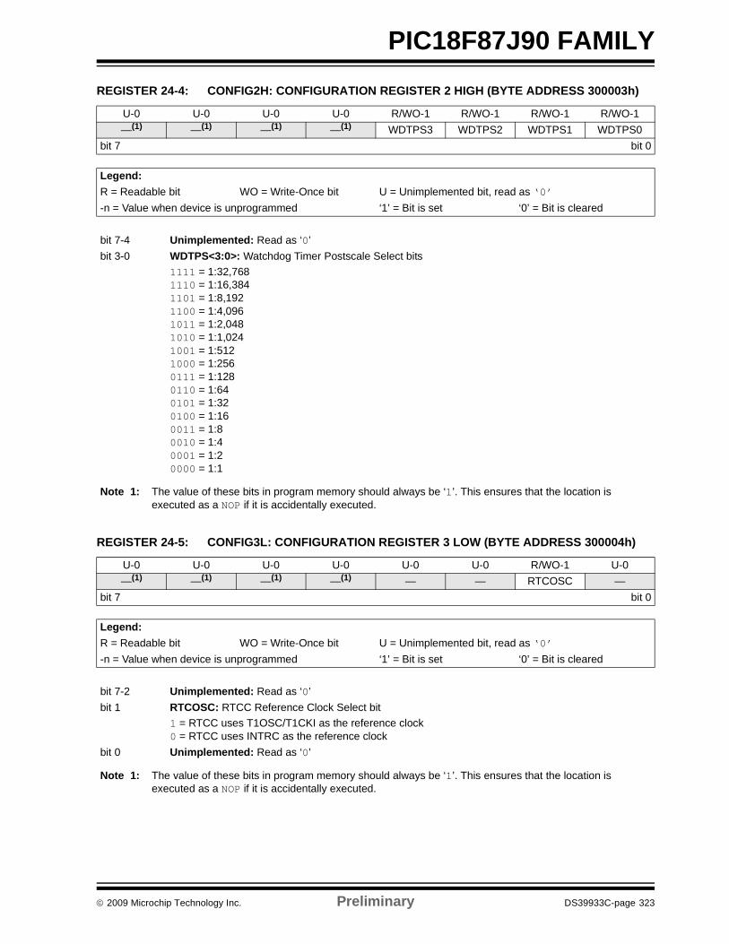
© 2009 Microchip Technology Inc. Preliminary DS39933C-page 323
PIC18F87J90 FAMILY REGISTER 24-4: CONFIG2H: CONFIGURATION REGISTER 2 HIGH (BYTE ADDRESS 300003h)
U-0 U-0 U-0 U-0 R/WO-1 R/WO-1 R/WO-1 R/WO-1—(1) —(1) —(1) —(1) WDTPS3 WDTPS2 WDTPS1 WDTPS0
bit 7 bit 0
Legend:R = Readable bit WO = Write-Once bit U = Unimplemented bit, read as ‘0’-n = Value when device is unprogrammed ‘1’ = Bit is set ‘0’ = Bit is cleared
bit 7-4 Unimplemented: Read as ‘0’ bit 3-0 WDTPS<3:0>: Watchdog Timer Postscale Select bits
1111 = 1:32,7681110 = 1:16,3841101 = 1:8,1921100 = 1:4,0961011 = 1:2,0481010 = 1:1,0241001 = 1:5121000 = 1:2560111 = 1:1280110 = 1:640101 = 1:320100 = 1:160011 = 1:80010 = 1:40001 = 1:20000 = 1:1
Note 1: The value of these bits in program memory should always be ‘1’. This ensures that the location is executed as a NOP if it is accidentally executed.
REGISTER 24-5: CONFIG3L: CONFIGURATION REGISTER 3 LOW (BYTE ADDRESS 300004h)
U-0 U-0 U-0 U-0 U-0 U-0 R/WO-1 U-0—(1) —(1) —(1) —(1) — — RTCOSC —
bit 7 bit 0
Legend:R = Readable bit WO = Write-Once bit U = Unimplemented bit, read as ‘0’-n = Value when device is unprogrammed ‘1’ = Bit is set ‘0’ = Bit is cleared
bit 7-2 Unimplemented: Read as ‘0’ bit 1 RTCOSC: RTCC Reference Clock Select bit
1 = RTCC uses T1OSC/T1CKI as the reference clock0 = RTCC uses INTRC as the reference clock
bit 0 Unimplemented: Read as ‘0’
Note 1: The value of these bits in program memory should always be ‘1’. This ensures that the location is executed as a NOP if it is accidentally executed.
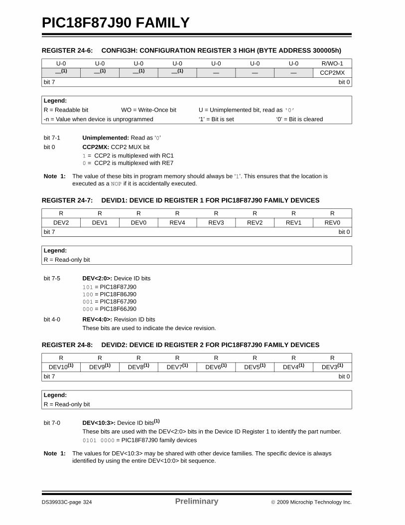
PIC18F87J90 FAMILY
DS39933C-page 324 Preliminary © 2009 Microchip Technology Inc.
REGISTER 24-6: CONFIG3H: CONFIGURATION REGISTER 3 HIGH (BYTE ADDRESS 300005h)
U-0 U-0 U-0 U-0 U-0 U-0 U-0 R/WO-1—(1) —(1) —(1) —(1) — — — CCP2MX
bit 7 bit 0
Legend:R = Readable bit WO = Write-Once bit U = Unimplemented bit, read as ‘0’-n = Value when device is unprogrammed ‘1’ = Bit is set ‘0’ = Bit is cleared
bit 7-1 Unimplemented: Read as ‘0’bit 0 CCP2MX: CCP2 MUX bit
1 = CCP2 is multiplexed with RC10 = CCP2 is multiplexed with RE7
Note 1: The value of these bits in program memory should always be ‘1’. This ensures that the location is executed as a NOP if it is accidentally executed.
REGISTER 24-7: DEVID1: DEVICE ID REGISTER 1 FOR PIC18F87J90 FAMILY DEVICES
R R R R R R R RDEV2 DEV1 DEV0 REV4 REV3 REV2 REV1 REV0
bit 7 bit 0
Legend:R = Read-only bit
bit 7-5 DEV<2:0>: Device ID bits101 = PIC18F87J90100 = PIC18F86J90001 = PIC18F67J90000 = PIC18F66J90
bit 4-0 REV<4:0>: Revision ID bitsThese bits are used to indicate the device revision.
REGISTER 24-8: DEVID2: DEVICE ID REGISTER 2 FOR PIC18F87J90 FAMILY DEVICES
R R R R R R R RDEV10(1) DEV9(1) DEV8(1) DEV7(1) DEV6(1) DEV5(1) DEV4(1) DEV3(1)
bit 7 bit 0
Legend:R = Read-only bit
bit 7-0 DEV<10:3>: Device ID bits(1)
These bits are used with the DEV<2:0> bits in the Device ID Register 1 to identify the part number.0101 0000 = PIC18F87J90 family devices
Note 1: The values for DEV<10:3> may be shared with other device families. The specific device is always identified by using the entire DEV<10:0> bit sequence.
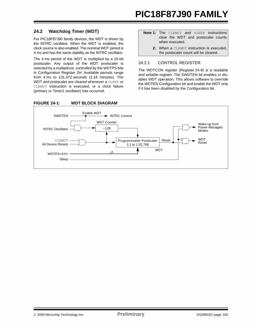
© 2009 Microchip Technology Inc. Preliminary DS39933C-page 325
PIC18F87J90 FAMILY24.2 Watchdog Timer (WDT)For PIC18F87J90 family devices, the WDT is driven bythe INTRC oscillator. When the WDT is enabled, theclock source is also enabled. The nominal WDT period is4 ms and has the same stability as the INTRC oscillator.
The 4 ms period of the WDT is multiplied by a 16-bitpostscaler. Any output of the WDT postscaler isselected by a multiplexor, controlled by the WDTPS bitsin Configuration Register 2H. Available periods rangefrom 4 ms to 131.072 seconds (2.18 minutes). TheWDT and postscaler are cleared whenever a SLEEP orCLRWDT instruction is executed, or a clock failure(primary or Timer1 oscillator) has occurred.
24.2.1 CONTROL REGISTER
The WDTCON register (Register 24-9) is a readableand writable register. The SWDTEN bit enables or dis-ables WDT operation. This allows software to overridethe WDTEN Configuration bit and enable the WDT onlyif it has been disabled by the Configuration bit.
FIGURE 24-1: WDT BLOCK DIAGRAM
Note 1: The CLRWDT and SLEEP instructionsclear the WDT and postscaler countswhen executed.
2: When a CLRWDT instruction is executed,the postscaler count will be cleared.
INTRC Oscillator
WDT
Wake-up from
Reset
WDT
WDT Counter
Programmable Postscaler1:1 to 1:32,768
Enable WDT
WDTPS<3:0>
SWDTEN
CLRWDT
4
Power-Managed
ResetAll Device Resets
Sleep
INTRC Control
÷128Modes
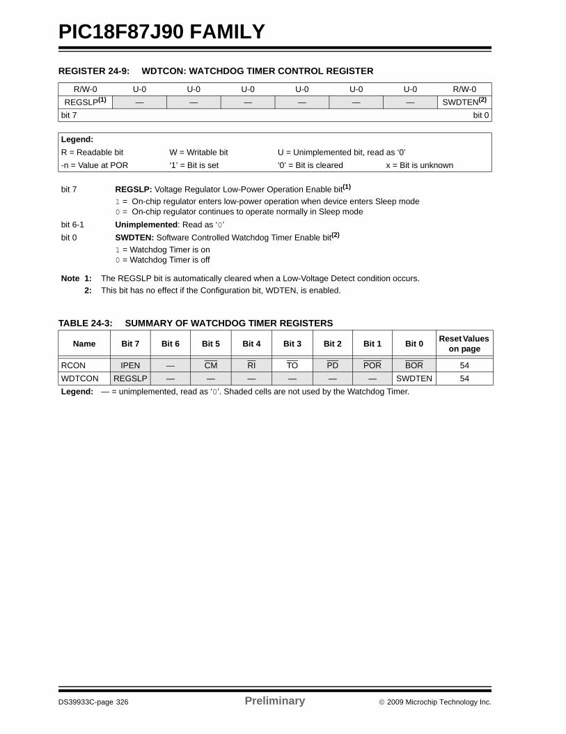
PIC18F87J90 FAMILY
DS39933C-page 326 Preliminary © 2009 Microchip Technology Inc.
TABLE 24-3: SUMMARY OF WATCHDOG TIMER REGISTERS
REGISTER 24-9: WDTCON: WATCHDOG TIMER CONTROL REGISTER
R/W-0 U-0 U-0 U-0 U-0 U-0 U-0 R/W-0REGSLP(1) — — — — — — SWDTEN(2)
bit 7 bit 0
Legend:R = Readable bit W = Writable bit U = Unimplemented bit, read as ‘0’-n = Value at POR ‘1’ = Bit is set ‘0’ = Bit is cleared x = Bit is unknown
bit 7 REGSLP: Voltage Regulator Low-Power Operation Enable bit(1) 1 = On-chip regulator enters low-power operation when device enters Sleep mode0 = On-chip regulator continues to operate normally in Sleep mode
bit 6-1 Unimplemented: Read as ‘0’bit 0 SWDTEN: Software Controlled Watchdog Timer Enable bit(2)
1 = Watchdog Timer is on0 = Watchdog Timer is off
Note 1: The REGSLP bit is automatically cleared when a Low-Voltage Detect condition occurs.2: This bit has no effect if the Configuration bit, WDTEN, is enabled.
Name Bit 7 Bit 6 Bit 5 Bit 4 Bit 3 Bit 2 Bit 1 Bit 0 Reset Values on page
RCON IPEN — CM RI TO PD POR BOR 54WDTCON REGSLP — — — — — — SWDTEN 54Legend: — = unimplemented, read as ‘0’. Shaded cells are not used by the Watchdog Timer.
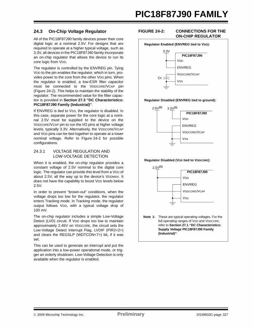
© 2009 Microchip Technology Inc. Preliminary DS39933C-page 327
PIC18F87J90 FAMILY24.3 On-Chip Voltage RegulatorAll of the PIC18F87J90 family devices power their coredigital logic at a nominal 2.5V. For designs that arerequired to operate at a higher typical voltage, such as3.3V, all devices in the PIC18F87J90 family incorporatean on-chip regulator that allows the device to run itscore logic from VDD.
The regulator is controlled by the ENVREG pin. TyingVDD to the pin enables the regulator, which in turn, pro-vides power to the core from the other VDD pins. Whenthe regulator is enabled, a low-ESR filter capacitormust be connected to the VDDCORE/VCAP pin(Figure 24-2). This helps to maintain the stability of theregulator. The recommended value for the filter capac-itor is provided in Section 27.3 “DC Characteristics:PIC18F87J90 Family (Industrial)”.
If ENVREG is tied to VSS, the regulator is disabled. Inthis case, separate power for the core logic at a nomi-nal 2.5V must be supplied to the device on theVDDCORE/VCAP pin to run the I/O pins at higher voltagelevels, typically 3.3V. Alternatively, the VDDCORE/VCAPand VDD pins can be tied together to operate at a lowernominal voltage. Refer to Figure 24-2 for possibleconfigurations.
24.3.1 VOLTAGE REGULATION AND LOW-VOLTAGE DETECTION
When it is enabled, the on-chip regulator provides aconstant voltage of 2.5V nominal to the digital corelogic. The regulator can provide this level from a VDD ofabout 2.5V, all the way up to the device’s VDDMAX. Itdoes not have the capability to boost VDD levels below2.5V.
In order to prevent “brown-out” conditions, when thevoltage drops too low for the regulator, the regulatorenters Tracking mode. In Tracking mode, the regulatoroutput follows VDD, with a typical voltage drop of100 mV.
The on-chip regulator includes a simple Low-VoltageDetect (LVD) circuit. If VDD drops too low to maintainapproximately 2.45V on VDDCORE, the circuit sets theLow-Voltage Detect Interrupt Flag, LVDIF (PIR2<2>)and clears the REGSLP (WDTCON<7>) bit, if it wasset.
This can be used to generate an interrupt and put theapplication into a low-power operational mode, or trig-ger an orderly shutdown. Low-Voltage Detection is onlyavailable when the regulator is enabled.
FIGURE 24-2: CONNECTIONS FOR THE ON-CHIP REGULATOR
VDD
ENVREG
VDDCORE/VCAP
VSS
3.3V(1)2.5V(1)
VDD
ENVREG
VDDCORE/VCAP
VSSCF
3.3V
Regulator Enabled (ENVREG tied to VDD):
Regulator Disabled (ENVREG tied to ground):
VDD
ENVREG
VDDCORE/VCAP
VSS
2.5V(1)
Regulator Disabled (VDD tied to VDDCORE):
Note 1: These are typical operating voltages. For the full operating ranges of VDD and VDDCORE, refer to Section 27.1 “DC Characteristics: Supply Voltage PIC18F87J90 Family (Industrial)”.
PIC18F87J90
PIC18F87J90
PIC18F87J90
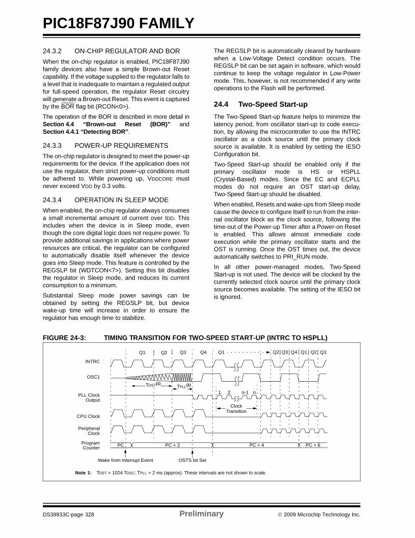
PIC18F87J90 FAMILY
DS39933C-page 328 Preliminary © 2009 Microchip Technology Inc.
24.3.2 ON-CHIP REGULATOR AND BORWhen the on-chip regulator is enabled, PIC18F87J90family devices also have a simple Brown-out Resetcapability. If the voltage supplied to the regulator falls toa level that is inadequate to maintain a regulated outputfor full-speed operation, the regulator Reset circuitrywill generate a Brown-out Reset. This event is capturedby the BOR flag bit (RCON<0>).
The operation of the BOR is described in more detail inSection 4.4 “Brown-out Reset (BOR)” andSection 4.4.1 “Detecting BOR”.
24.3.3 POWER-UP REQUIREMENTSThe on-chip regulator is designed to meet the power-uprequirements for the device. If the application does notuse the regulator, then strict power-up conditions mustbe adhered to. While powering up, VDDCORE mustnever exceed VDD by 0.3 volts.
24.3.4 OPERATION IN SLEEP MODEWhen enabled, the on-chip regulator always consumesa small incremental amount of current over IDD. Thisincludes when the device is in Sleep mode, eventhough the core digital logic does not require power. Toprovide additional savings in applications where powerresources are critical, the regulator can be configuredto automatically disable itself whenever the devicegoes into Sleep mode. This feature is controlled by theREGSLP bit (WDTCON<7>). Setting this bit disablesthe regulator in Sleep mode, and reduces its currentconsumption to a minimum.
Substantial Sleep mode power savings can beobtained by setting the REGSLP bit, but devicewake-up time will increase in order to ensure theregulator has enough time to stabilize.
The REGSLP bit is automatically cleared by hardwarewhen a Low-Voltage Detect condition occurs. TheREGSLP bit can be set again in software, which wouldcontinue to keep the voltage regulator in Low-Powermode. This, however, is not recommended if any writeoperations to the Flash will be performed.
24.4 Two-Speed Start-upThe Two-Speed Start-up feature helps to minimize thelatency period, from oscillator start-up to code execu-tion, by allowing the microcontroller to use the INTRCoscillator as a clock source until the primary clocksource is available. It is enabled by setting the IESOConfiguration bit.
Two-Speed Start-up should be enabled only if theprimary oscillator mode is HS or HSPLL(Crystal-Based) modes. Since the EC and ECPLLmodes do not require an OST start-up delay,Two-Speed Start-up should be disabled.
When enabled, Resets and wake-ups from Sleep modecause the device to configure itself to run from the inter-nal oscillator block as the clock source, following thetime-out of the Power-up Timer after a Power-on Resetis enabled. This allows almost immediate codeexecution while the primary oscillator starts and theOST is running. Once the OST times out, the deviceautomatically switches to PRI_RUN mode.
In all other power-managed modes, Two-SpeedStart-up is not used. The device will be clocked by thecurrently selected clock source until the primary clocksource becomes available. The setting of the IESO bitis ignored.
FIGURE 24-3: TIMING TRANSITION FOR TWO-SPEED START-UP (INTRC TO HSPLL)
Q1 Q3 Q4
OSC1
Peripheral
Program PC PC + 2
INTRC
PLL Clock
Q1
PC + 6
Q2
Output
Q3 Q4 Q1
CPU Clock
PC + 4
Clock
Counter
Q2 Q2 Q3
Note 1: TOST = 1024 TOSC; TPLL = 2 ms (approx). These intervals are not shown to scale.
Wake from Interrupt Event
TPLL(1)
1 2 n-1 n
Clock
OSTS bit Set
Transition
TOST(1)
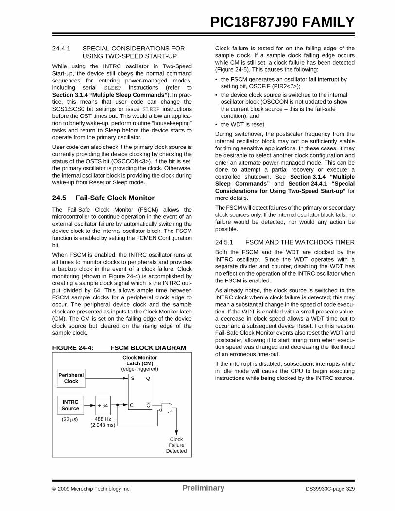
© 2009 Microchip Technology Inc. Preliminary DS39933C-page 329
PIC18F87J90 FAMILY24.4.1 SPECIAL CONSIDERATIONS FOR
USING TWO-SPEED START-UPWhile using the INTRC oscillator in Two-SpeedStart-up, the device still obeys the normal commandsequences for entering power-managed modes,including serial SLEEP instructions (refer toSection 3.1.4 “Multiple Sleep Commands”). In prac-tice, this means that user code can change theSCS1:SCS0 bit settings or issue SLEEP instructionsbefore the OST times out. This would allow an applica-tion to briefly wake-up, perform routine “housekeeping”tasks and return to Sleep before the device starts tooperate from the primary oscillator.
User code can also check if the primary clock source iscurrently providing the device clocking by checking thestatus of the OSTS bit (OSCCON<3>). If the bit is set,the primary oscillator is providing the clock. Otherwise,the internal oscillator block is providing the clock duringwake-up from Reset or Sleep mode.
24.5 Fail-Safe Clock MonitorThe Fail-Safe Clock Monitor (FSCM) allows themicrocontroller to continue operation in the event of anexternal oscillator failure by automatically switching thedevice clock to the internal oscillator block. The FSCMfunction is enabled by setting the FCMEN Configurationbit.
When FSCM is enabled, the INTRC oscillator runs atall times to monitor clocks to peripherals and providesa backup clock in the event of a clock failure. Clockmonitoring (shown in Figure 24-4) is accomplished bycreating a sample clock signal which is the INTRC out-put divided by 64. This allows ample time betweenFSCM sample clocks for a peripheral clock edge tooccur. The peripheral device clock and the sampleclock are presented as inputs to the Clock Monitor latch(CM). The CM is set on the falling edge of the deviceclock source but cleared on the rising edge of thesample clock.
FIGURE 24-4: FSCM BLOCK DIAGRAM
Clock failure is tested for on the falling edge of thesample clock. If a sample clock falling edge occurswhile CM is still set, a clock failure has been detected(Figure 24-5). This causes the following:
• the FSCM generates an oscillator fail interrupt by setting bit, OSCFIF (PIR2<7>);
• the device clock source is switched to the internal oscillator block (OSCCON is not updated to show the current clock source – this is the fail-safe condition); and
• the WDT is reset.
During switchover, the postscaler frequency from theinternal oscillator block may not be sufficiently stablefor timing sensitive applications. In these cases, it maybe desirable to select another clock configuration andenter an alternate power-managed mode. This can bedone to attempt a partial recovery or execute acontrolled shutdown. See Section 3.1.4 “MultipleSleep Commands” and Section 24.4.1 “SpecialConsiderations for Using Two-Speed Start-up” formore details.
The FSCM will detect failures of the primary or secondaryclock sources only. If the internal oscillator block fails, nofailure would be detected, nor would any action bepossible.
24.5.1 FSCM AND THE WATCHDOG TIMERBoth the FSCM and the WDT are clocked by theINTRC oscillator. Since the WDT operates with aseparate divider and counter, disabling the WDT hasno effect on the operation of the INTRC oscillator whenthe FSCM is enabled.
As already noted, the clock source is switched to theINTRC clock when a clock failure is detected; this maymean a substantial change in the speed of code execu-tion. If the WDT is enabled with a small prescale value,a decrease in clock speed allows a WDT time-out tooccur and a subsequent device Reset. For this reason,Fail-Safe Clock Monitor events also reset the WDT andpostscaler, allowing it to start timing from when execu-tion speed was changed and decreasing the likelihoodof an erroneous time-out.
If the interrupt is disabled, subsequent interrupts whilein Idle mode will cause the CPU to begin executinginstructions while being clocked by the INTRC source.Peripheral
INTRC÷ 64
S
C
Q
(32 μs) 488 Hz(2.048 ms)
Clock MonitorLatch (CM)
(edge-triggered)
ClockFailure
Detected
Source
Clock
Q
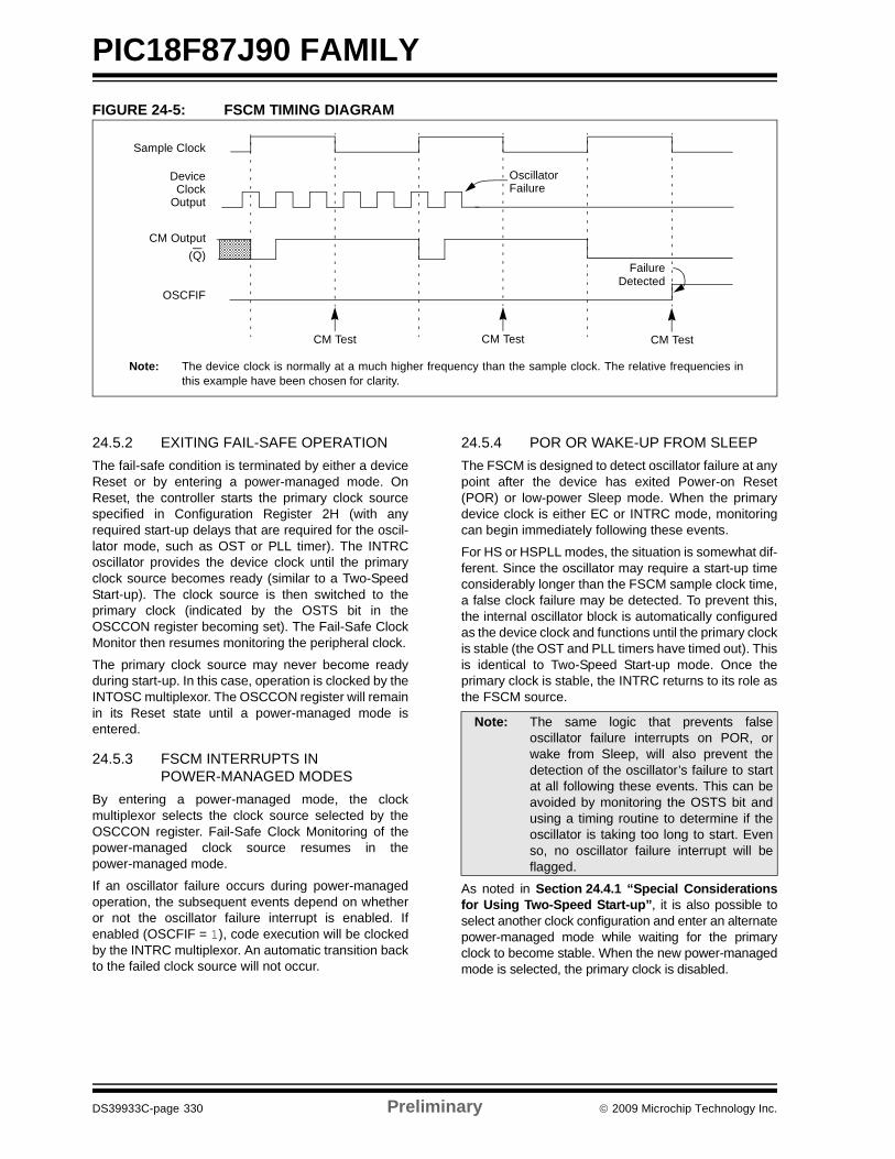
PIC18F87J90 FAMILY
DS39933C-page 330 Preliminary © 2009 Microchip Technology Inc.
FIGURE 24-5: FSCM TIMING DIAGRAM
24.5.2 EXITING FAIL-SAFE OPERATIONThe fail-safe condition is terminated by either a deviceReset or by entering a power-managed mode. OnReset, the controller starts the primary clock sourcespecified in Configuration Register 2H (with anyrequired start-up delays that are required for the oscil-lator mode, such as OST or PLL timer). The INTRCoscillator provides the device clock until the primaryclock source becomes ready (similar to a Two-SpeedStart-up). The clock source is then switched to theprimary clock (indicated by the OSTS bit in theOSCCON register becoming set). The Fail-Safe ClockMonitor then resumes monitoring the peripheral clock.
The primary clock source may never become readyduring start-up. In this case, operation is clocked by theINTOSC multiplexor. The OSCCON register will remainin its Reset state until a power-managed mode isentered.
24.5.3 FSCM INTERRUPTS IN POWER-MANAGED MODES
By entering a power-managed mode, the clockmultiplexor selects the clock source selected by theOSCCON register. Fail-Safe Clock Monitoring of thepower-managed clock source resumes in thepower-managed mode.
If an oscillator failure occurs during power-managedoperation, the subsequent events depend on whetheror not the oscillator failure interrupt is enabled. Ifenabled (OSCFIF = 1), code execution will be clockedby the INTRC multiplexor. An automatic transition backto the failed clock source will not occur.
24.5.4 POR OR WAKE-UP FROM SLEEPThe FSCM is designed to detect oscillator failure at anypoint after the device has exited Power-on Reset(POR) or low-power Sleep mode. When the primarydevice clock is either EC or INTRC mode, monitoringcan begin immediately following these events.
For HS or HSPLL modes, the situation is somewhat dif-ferent. Since the oscillator may require a start-up timeconsiderably longer than the FSCM sample clock time,a false clock failure may be detected. To prevent this,the internal oscillator block is automatically configuredas the device clock and functions until the primary clockis stable (the OST and PLL timers have timed out). Thisis identical to Two-Speed Start-up mode. Once theprimary clock is stable, the INTRC returns to its role asthe FSCM source.
As noted in Section 24.4.1 “Special Considerationsfor Using Two-Speed Start-up”, it is also possible toselect another clock configuration and enter an alternatepower-managed mode while waiting for the primaryclock to become stable. When the new power-managedmode is selected, the primary clock is disabled.
OSCFIF
CM Output
DeviceClock
Output
Sample Clock
FailureDetected
OscillatorFailure
Note: The device clock is normally at a much higher frequency than the sample clock. The relative frequencies inthis example have been chosen for clarity.
(Q)
CM Test CM Test CM Test
Note: The same logic that prevents falseoscillator failure interrupts on POR, orwake from Sleep, will also prevent thedetection of the oscillator’s failure to startat all following these events. This can beavoided by monitoring the OSTS bit andusing a timing routine to determine if theoscillator is taking too long to start. Evenso, no oscillator failure interrupt will beflagged.
© 2009 Microchip Technology Inc. Preliminary DS39933C-page 331
PIC18F87J90 FAMILY24.6 Program Verification and
Code ProtectionFor all devices in the PIC18F87J90 family of devices,the on-chip program memory space is treated as asingle block. Code protection for this block is controlledby one Configuration bit, CP0. This bit inhibits externalreads and writes to the program memory space. It hasno direct effect in normal execution mode.
24.6.1 CONFIGURATION REGISTER PROTECTION
The Configuration registers are protected againstuntoward changes or reads in two ways. The primaryprotection is the write-once feature of the Configurationbits which prevents reconfiguration once the bit hasbeen programmed during a power cycle. To safeguardagainst unpredictable events, Configuration bitchanges resulting from individual cell-level disruptions(such as ESD events) will cause a parity error andtrigger a device Reset.
The data for the Configuration registers is derived fromthe Flash Configuration Words in program memory.When the CP0 bit set, the source data for deviceconfiguration is also protected as a consequence.
24.7 In-Circuit Serial ProgrammingPIC18F87J90 family microcontrollers can be seriallyprogrammed while in the end application circuit. This issimply done with two lines for clock and data and threeother lines for power, ground and the programmingvoltage. This allows customers to manufacture boardswith unprogrammed devices and then program themicrocontroller just before shipping the product. Thisalso allows the most recent firmware or a customfirmware to be programmed.
24.8 In-Circuit DebuggerWhen the DEBUG Configuration bit is programmed toa ‘0’, the In-Circuit Debugger functionality is enabled.This function allows simple debugging functions whenused with MPLAB® IDE. When the microcontroller hasthis feature enabled, some resources are not availablefor general use. Table 24-4 shows which resources arerequired by the background debugger.
TABLE 24-4: DEBUGGER RESOURCES I/O pins: RB6, RB7Stack: 2 levelsProgram Memory: 512 bytesData Memory: 10 bytes

PIC18F87J90 FAMILY
DS39933C-page 332 Preliminary © 2009 Microchip Technology Inc.
NOTES:
© 2009 Microchip Technology Inc. Preliminary DS39933C-page 333
PIC18F87J90 FAMILY
25.0 INSTRUCTION SET SUMMARYThe PIC18F87J90 family of devices incorporate thestandard set of 75 PIC18 core instructions, as well asan extended set of 8 new instructions for the optimiza-tion of code that is recursive or that utilizes a softwarestack. The extended set is discussed later in thissection.
25.1 Standard Instruction SetThe standard PIC18 MCU instruction set adds manyenhancements to the previous PIC® MCU instructionsets, while maintaining an easy migration from thesePIC MCU instruction sets. Most instructions are asingle program memory word (16 bits), but there arefour instructions that require two program memorylocations.
Each single-word instruction is a 16-bit word dividedinto an opcode, which specifies the instruction type andone or more operands, which further specify theoperation of the instruction.
The instruction set is highly orthogonal and is groupedinto four basic categories:
• Byte-oriented operations• Bit-oriented operations• Literal operations• Control operations
The PIC18 instruction set summary in Table 25-2 listsbyte-oriented, bit-oriented, literal and controloperations. Table 25-1 shows the opcode fielddescriptions.
Most byte-oriented instructions have three operands:
1. The file register (specified by ‘f’) 2. The destination of the result (specified by ‘d’) 3. The accessed memory (specified by ‘a’)
The file register designator, ‘f’, specifies which file reg-ister is to be used by the instruction. The destinationdesignator, ‘d’, specifies where the result of theoperation is to be placed. If ‘d’ is zero, the result isplaced in the WREG register. If ‘d’ is one, the result isplaced in the file register specified in the instruction.
All bit-oriented instructions have three operands:
1. The file register (specified by ‘f’) 2. The bit in the file register (specified by ‘b’) 3. The accessed memory (specified by ‘a’)
The bit field designator, ‘b’, selects the number of the bitaffected by the operation, while the file register desig-nator, ‘f’, represents the number of the file in which thebit is located.
The literal instructions may use some of the followingoperands:
• A literal value to be loaded into a file register (specified by ‘k’)
• The desired FSR register to load the literal value into (specified by ‘f’)
• No operand required (specified by ‘—’)
The control instructions may use some of the followingoperands:
• A program memory address (specified by ‘n’)• The mode of the CALL or RETURN instructions
(specified by ‘s’)• The mode of the table read and table write
instructions (specified by ‘m’)• No operand required
(specified by ‘—’)
All instructions are a single word, except for fourdouble-word instructions. These instructions weremade double-word to contain the required informationin 32 bits. In the second word, the 4 MSbs are ‘1’s. Ifthis second word is executed as an instruction (byitself), it will execute as a NOP.
All single-word instructions are executed in a singleinstruction cycle, unless a conditional test is true or theprogram counter is changed as a result of the instruc-tion. In these cases, the execution takes two instructioncycles with the additional instruction cycle(s) executedas a NOP.
The double-word instructions execute in two instructioncycles.
One instruction cycle consists of four oscillator periods.Thus, for an oscillator frequency of 4 MHz, the normalinstruction execution time is 1 μs. If a conditional test istrue, or the program counter is changed as a result ofan instruction, the instruction execution time is 2 μs.Two-word branch instructions (if true) would take 3 μs.
Figure 25-1 shows the general formats that the instruc-tions can have. All examples use the convention ‘nnh’to represent a hexadecimal number.
The Instruction Set Summary, shown in Table 25-2,lists the standard instructions recognized by theMicrochip MPASMTM Assembler.
Section 25.1.1 “Standard Instruction Set” providesa description of each instruction.
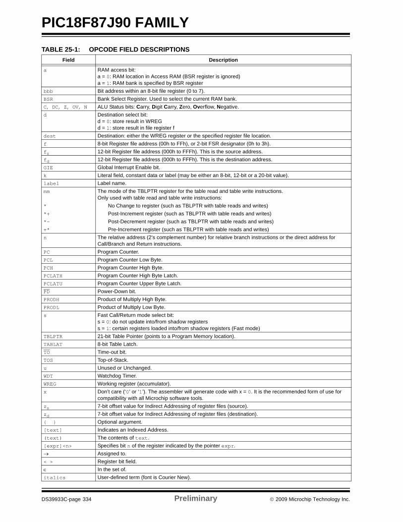
PIC18F87J90 FAMILY
DS39933C-page 334 Preliminary © 2009 Microchip Technology Inc.
TABLE 25-1: OPCODE FIELD DESCRIPTIONS Field Description
a RAM access bit:a = 0: RAM location in Access RAM (BSR register is ignored)a = 1: RAM bank is specified by BSR register
bbb Bit address within an 8-bit file register (0 to 7).BSR Bank Select Register. Used to select the current RAM bank.C, DC, Z, OV, N ALU Status bits: Carry, Digit Carry, Zero, Overflow, Negative.d Destination select bit:
d = 0: store result in WREGd = 1: store result in file register f
dest Destination: either the WREG register or the specified register file location.f 8-bit Register file address (00h to FFh), or 2-bit FSR designator (0h to 3h).fs 12-bit Register file address (000h to FFFh). This is the source address. fd 12-bit Register file address (000h to FFFh). This is the destination address. GIE Global Interrupt Enable bit.k Literal field, constant data or label (may be either an 8-bit, 12-bit or a 20-bit value).label Label name.mm The mode of the TBLPTR register for the table read and table write instructions.
Only used with table read and table write instructions:* No Change to register (such as TBLPTR with table reads and writes)*+ Post-Increment register (such as TBLPTR with table reads and writes)*- Post-Decrement register (such as TBLPTR with table reads and writes)+* Pre-Increment register (such as TBLPTR with table reads and writes)n The relative address (2’s complement number) for relative branch instructions or the direct address for
Call/Branch and Return instructions.PC Program Counter.PCL Program Counter Low Byte.PCH Program Counter High Byte.PCLATH Program Counter High Byte Latch.PCLATU Program Counter Upper Byte Latch.PD Power-Down bit.PRODH Product of Multiply High Byte.PRODL Product of Multiply Low Byte.s Fast Call/Return mode select bit:
s = 0: do not update into/from shadow registerss = 1: certain registers loaded into/from shadow registers (Fast mode)
TBLPTR 21-bit Table Pointer (points to a Program Memory location).TABLAT 8-bit Table Latch.TO Time-out bit.TOS Top-of-Stack.u Unused or Unchanged.WDT Watchdog Timer.WREG Working register (accumulator).x Don’t care (‘0’ or ‘1’). The assembler will generate code with x = 0. It is the recommended form of use for
compatibility with all Microchip software tools.zs 7-bit offset value for Indirect Addressing of register files (source).zd 7-bit offset value for Indirect Addressing of register files (destination). Optional argument.[text] Indicates an Indexed Address.(text) The contents of text.[expr]<n> Specifies bit n of the register indicated by the pointer expr.→ Assigned to.< > Register bit field.∈ In the set of.italics User-defined term (font is Courier New).
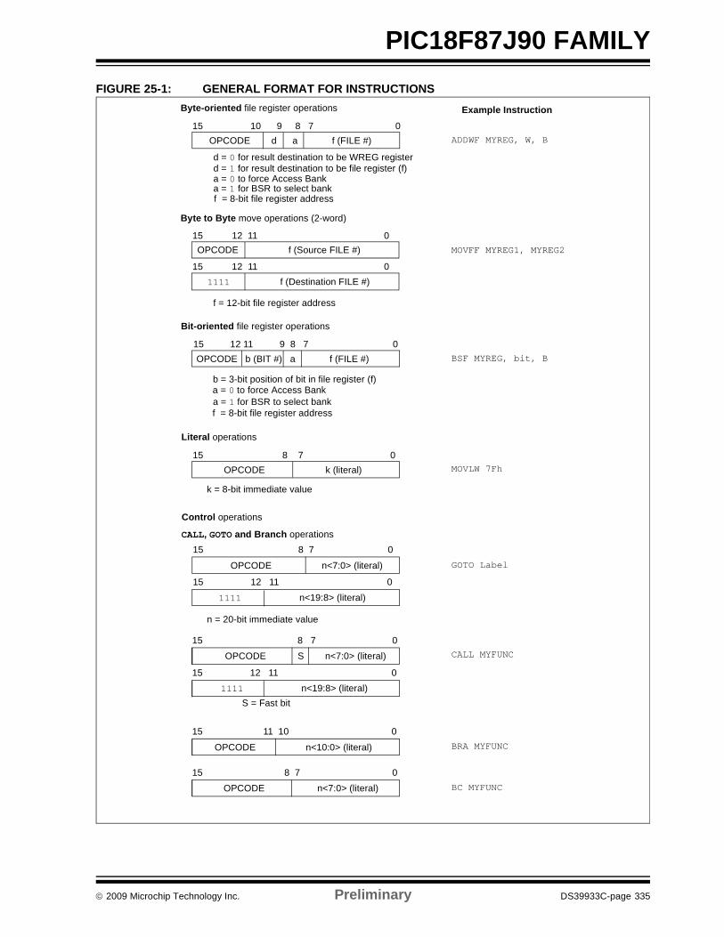
© 2009 Microchip Technology Inc. Preliminary DS39933C-page 335
PIC18F87J90 FAMILYFIGURE 25-1: GENERAL FORMAT FOR INSTRUCTIONS
Byte-oriented file register operations
15 10 9 8 7 0
d = 0 for result destination to be WREG register
OPCODE d a f (FILE #)
d = 1 for result destination to be file register (f)a = 0 to force Access Bank
Bit-oriented file register operations
15 12 11 9 8 7 0OPCODE b (BIT #) a f (FILE #)
b = 3-bit position of bit in file register (f)
Literal operations
15 8 7 0 OPCODE k (literal)
k = 8-bit immediate value
Byte to Byte move operations (2-word)
15 12 11 0OPCODE f (Source FILE #)
CALL, GOTO and Branch operations 15 8 7 0
OPCODE n<7:0> (literal)
n = 20-bit immediate value
a = 1 for BSR to select bankf = 8-bit file register address
a = 0 to force Access Banka = 1 for BSR to select bankf = 8-bit file register address
15 12 11 0
1111 n<19:8> (literal)
15 12 11 0 1111 f (Destination FILE #)
f = 12-bit file register address
Control operations
Example Instruction
ADDWF MYREG, W, B
MOVFF MYREG1, MYREG2
BSF MYREG, bit, B
MOVLW 7Fh
GOTO Label
15 8 7 0
OPCODE S n<7:0> (literal)
15 12 11 01111 n<19:8> (literal)
CALL MYFUNC
15 11 10 0
OPCODE n<10:0> (literal)
S = Fast bit
BRA MYFUNC
15 8 7 0
OPCODE n<7:0> (literal) BC MYFUNC
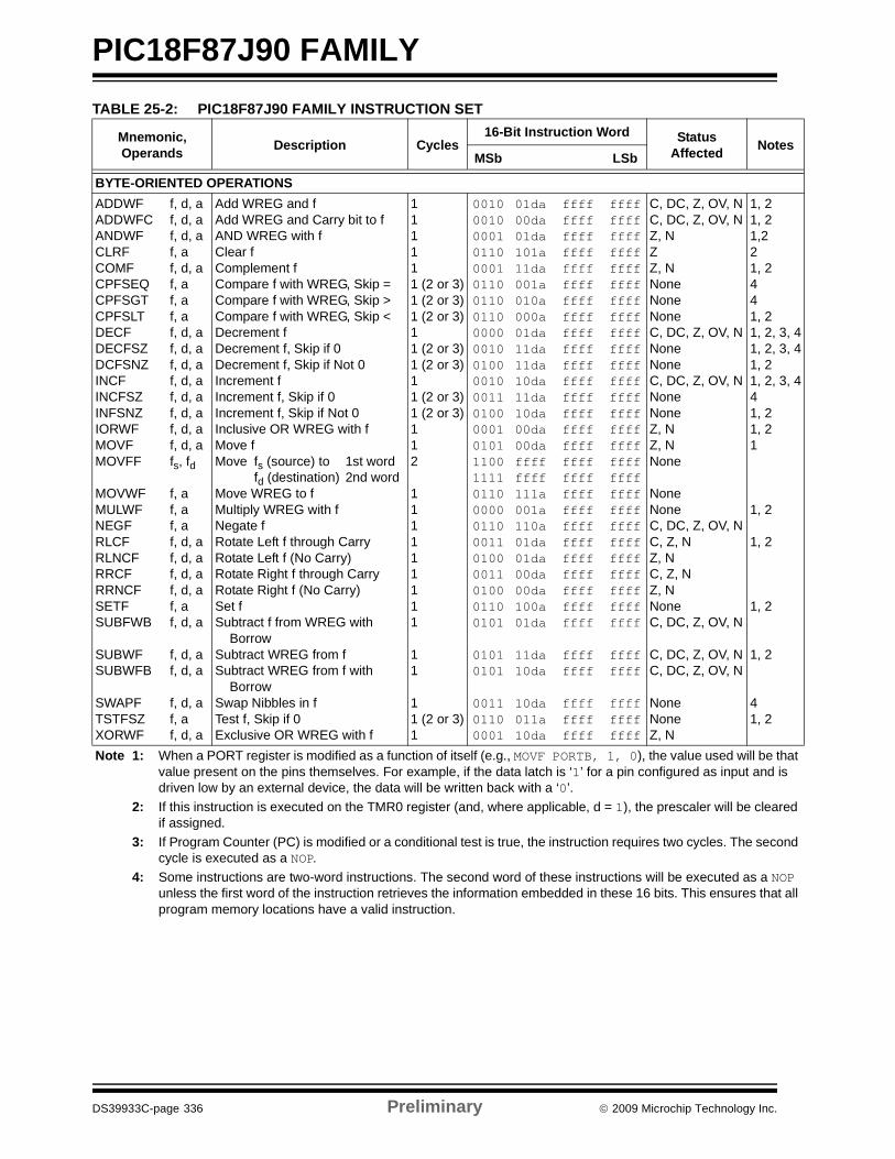
PIC18F87J90 FAMILY
DS39933C-page 336 Preliminary © 2009 Microchip Technology Inc.
TABLE 25-2: PIC18F87J90 FAMILY INSTRUCTION SET
Mnemonic,Operands Description Cycles
16-Bit Instruction Word StatusAffected Notes
MSb LSb
BYTE-ORIENTED OPERATIONSADDWFADDWFCANDWFCLRFCOMFCPFSEQCPFSGTCPFSLTDECFDECFSZDCFSNZINCFINCFSZINFSNZIORWFMOVFMOVFF
MOVWFMULWFNEGFRLCFRLNCFRRCFRRNCFSETFSUBFWB
SUBWFSUBWFB
SWAPFTSTFSZXORWF
f, d, af, d, af, d, af, af, d, af, af, af, af, d, af, d, af, d, af, d, af, d, af, d, af, d, af, d, afs, fd
f, af, af, af, d, af, d, af, d, af, d, af, af, d, a
f, d, af, d, a
f, d, af, af, d, a
Add WREG and fAdd WREG and Carry bit to fAND WREG with fClear fComplement fCompare f with WREG, Skip =Compare f with WREG, Skip >Compare f with WREG, Skip <Decrement fDecrement f, Skip if 0Decrement f, Skip if Not 0Increment fIncrement f, Skip if 0Increment f, Skip if Not 0Inclusive OR WREG with fMove fMove fs (source) to 1st word
fd (destination) 2nd wordMove WREG to fMultiply WREG with fNegate fRotate Left f through CarryRotate Left f (No Carry)Rotate Right f through CarryRotate Right f (No Carry)Set fSubtract f from WREG with Borrow Subtract WREG from fSubtract WREG from f with BorrowSwap Nibbles in fTest f, Skip if 0Exclusive OR WREG with f
111111 (2 or 3)1 (2 or 3)1 (2 or 3)11 (2 or 3)1 (2 or 3)11 (2 or 3)1 (2 or 3)112
111111111
11
11 (2 or 3)1
001000100001011000010110011001100000001001000010001101000001010111001111011000000110001101000011010001100101
01010101
001101100001
01da00da01da101a11da001a010a000a01da11da11da10da11da10da00da00daffffffff111a001a110a01da01da00da00da100a01da
11da10da
10da011a10da
ffffffffffffffffffffffffffffffffffffffffffffffffffffffffffffffffffffffffffffffffffffffffffffffffffffffffffff
ffffffff
ffffffffffff
ffffffffffffffffffffffffffffffffffffffffffffffffffffffffffffffffffffffffffffffffffffffffffffffffffffffffffff
ffffffff
ffffffffffff
C, DC, Z, OV, NC, DC, Z, OV, NZ, NZZ, NNoneNoneNoneC, DC, Z, OV, NNoneNoneC, DC, Z, OV, NNoneNoneZ, NZ, NNone
NoneNoneC, DC, Z, OV, NC, Z, NZ, NC, Z, NZ, NNoneC, DC, Z, OV, N
C, DC, Z, OV, NC, DC, Z, OV, N
NoneNoneZ, N
1, 21, 21,221, 2441, 21, 2, 3, 41, 2, 3, 41, 21, 2, 3, 441, 21, 21
1, 2
1, 2
1, 2
1, 2
41, 2
Note 1: When a PORT register is modified as a function of itself (e.g., MOVF PORTB, 1, 0), the value used will be that value present on the pins themselves. For example, if the data latch is ‘1’ for a pin configured as input and is driven low by an external device, the data will be written back with a ‘0’.
2: If this instruction is executed on the TMR0 register (and, where applicable, d = 1), the prescaler will be cleared if assigned.
3: If Program Counter (PC) is modified or a conditional test is true, the instruction requires two cycles. The second cycle is executed as a NOP.
4: Some instructions are two-word instructions. The second word of these instructions will be executed as a NOP unless the first word of the instruction retrieves the information embedded in these 16 bits. This ensures that all program memory locations have a valid instruction.
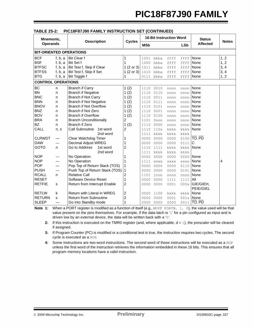
© 2009 Microchip Technology Inc. Preliminary DS39933C-page 337
PIC18F87J90 FAMILY
BIT-ORIENTED OPERATIONSBCFBSFBTFSCBTFSSBTG
f, b, af, b, af, b, af, b, af, b, a
Bit Clear fBit Set fBit Test f, Skip if ClearBit Test f, Skip if SetBit Toggle f
111 (2 or 3)1 (2 or 3)1
10011000101110100111
bbbabbbabbbabbbabbba
ffffffffffffffffffff
ffffffffffffffffffff
NoneNoneNoneNoneNone
1, 21, 23, 43, 41, 2
CONTROL OPERATIONSBCBNBNCBNNBNOVBNZBOVBRABZCALL
CLRWDTDAWGOTO
NOPNOPPOPPUSHRCALLRESETRETFIE
RETLWRETURNSLEEP
nnnnnnnnnn, s
——n
————n
s
ks—
Branch if CarryBranch if NegativeBranch if Not CarryBranch if Not NegativeBranch if Not OverflowBranch if Not ZeroBranch if OverflowBranch Unconditionally Branch if ZeroCall Subroutine 1st word
2nd wordClear Watchdog TimerDecimal Adjust WREGGo to Address 1st word
2nd wordNo OperationNo OperationPop Top of Return Stack (TOS)Push Top of Return Stack (TOS)Relative CallSoftware Device ResetReturn from Interrupt Enable
Return with Literal in WREG Return from SubroutineGo into Standby mode
1 (2)1 (2)1 (2)1 (2)1 (2)1 (2)1 (2)21 (2)2
112
1111212
221
1110111011101110111011101110110111101110111100000000111011110000111100000000110100000000
000000000000
00100110001101110101000101000nnn0000110skkkk000000001111kkkk0000xxxx000000001nnn00000000
110000000000
nnnnnnnnnnnnnnnnnnnnnnnnnnnnnnnnnnnnkkkkkkkk00000000kkkkkkkk0000xxxx00000000nnnn11110001
kkkk00010000
nnnnnnnnnnnnnnnnnnnnnnnnnnnnnnnnnnnnkkkkkkkk01000111kkkkkkkk0000xxxx01100101nnnn1111000s
kkkk001s0011
NoneNoneNoneNoneNoneNoneNoneNoneNoneNone
TO, PDCNone
NoneNoneNoneNoneNoneAllGIE/GIEH, PEIE/GIELNoneNoneTO, PD
4
TABLE 25-2: PIC18F87J90 FAMILY INSTRUCTION SET (CONTINUED)
Mnemonic,Operands Description Cycles
16-Bit Instruction Word StatusAffected Notes
MSb LSb
Note 1: When a PORT register is modified as a function of itself (e.g., MOVF PORTB, 1, 0), the value used will be that value present on the pins themselves. For example, if the data latch is ‘1’ for a pin configured as input and is driven low by an external device, the data will be written back with a ‘0’.
2: If this instruction is executed on the TMR0 register (and, where applicable, d = 1), the prescaler will be cleared if assigned.
3: If Program Counter (PC) is modified or a conditional test is true, the instruction requires two cycles. The second cycle is executed as a NOP.
4: Some instructions are two-word instructions. The second word of these instructions will be executed as a NOP unless the first word of the instruction retrieves the information embedded in these 16 bits. This ensures that all program memory locations have a valid instruction.
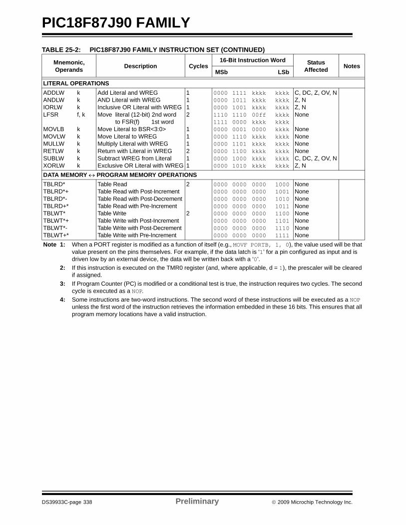
PIC18F87J90 FAMILY
DS39933C-page 338 Preliminary © 2009 Microchip Technology Inc.
LITERAL OPERATIONSADDLWANDLWIORLWLFSR
MOVLBMOVLWMULLWRETLWSUBLWXORLW
kkkf, k
kkkkkk
Add Literal and WREGAND Literal with WREGInclusive OR Literal with WREGMove literal (12-bit) 2nd word
to FSR(f) 1st wordMove Literal to BSR<3:0>Move Literal to WREGMultiply Literal with WREGReturn with Literal in WREG Subtract WREG from LiteralExclusive OR Literal with WREG
1112
111211
00000000000011101111000000000000000000000000
11111011100111100000000111101101110010001010
kkkkkkkkkkkk00ffkkkk0000kkkkkkkkkkkkkkkkkkkk
kkkkkkkkkkkkkkkkkkkkkkkkkkkkkkkkkkkkkkkkkkkk
C, DC, Z, OV, NZ, NZ, NNone
NoneNoneNoneNoneC, DC, Z, OV, NZ, N
DATA MEMORY ↔ PROGRAM MEMORY OPERATIONSTBLRD*TBLRD*+TBLRD*-TBLRD+*TBLWT*TBLWT*+TBLWT*-TBLWT+*
Table ReadTable Read with Post-IncrementTable Read with Post-DecrementTable Read with Pre-IncrementTable WriteTable Write with Post-IncrementTable Write with Post-DecrementTable Write with Pre-Increment
2
2
00000000000000000000000000000000
00000000000000000000000000000000
00000000000000000000000000000000
10001001101010111100110111101111
NoneNoneNoneNoneNoneNoneNoneNone
TABLE 25-2: PIC18F87J90 FAMILY INSTRUCTION SET (CONTINUED)
Mnemonic,Operands Description Cycles
16-Bit Instruction Word StatusAffected Notes
MSb LSb
Note 1: When a PORT register is modified as a function of itself (e.g., MOVF PORTB, 1, 0), the value used will be that value present on the pins themselves. For example, if the data latch is ‘1’ for a pin configured as input and is driven low by an external device, the data will be written back with a ‘0’.
2: If this instruction is executed on the TMR0 register (and, where applicable, d = 1), the prescaler will be cleared if assigned.
3: If Program Counter (PC) is modified or a conditional test is true, the instruction requires two cycles. The second cycle is executed as a NOP.
4: Some instructions are two-word instructions. The second word of these instructions will be executed as a NOP unless the first word of the instruction retrieves the information embedded in these 16 bits. This ensures that all program memory locations have a valid instruction.
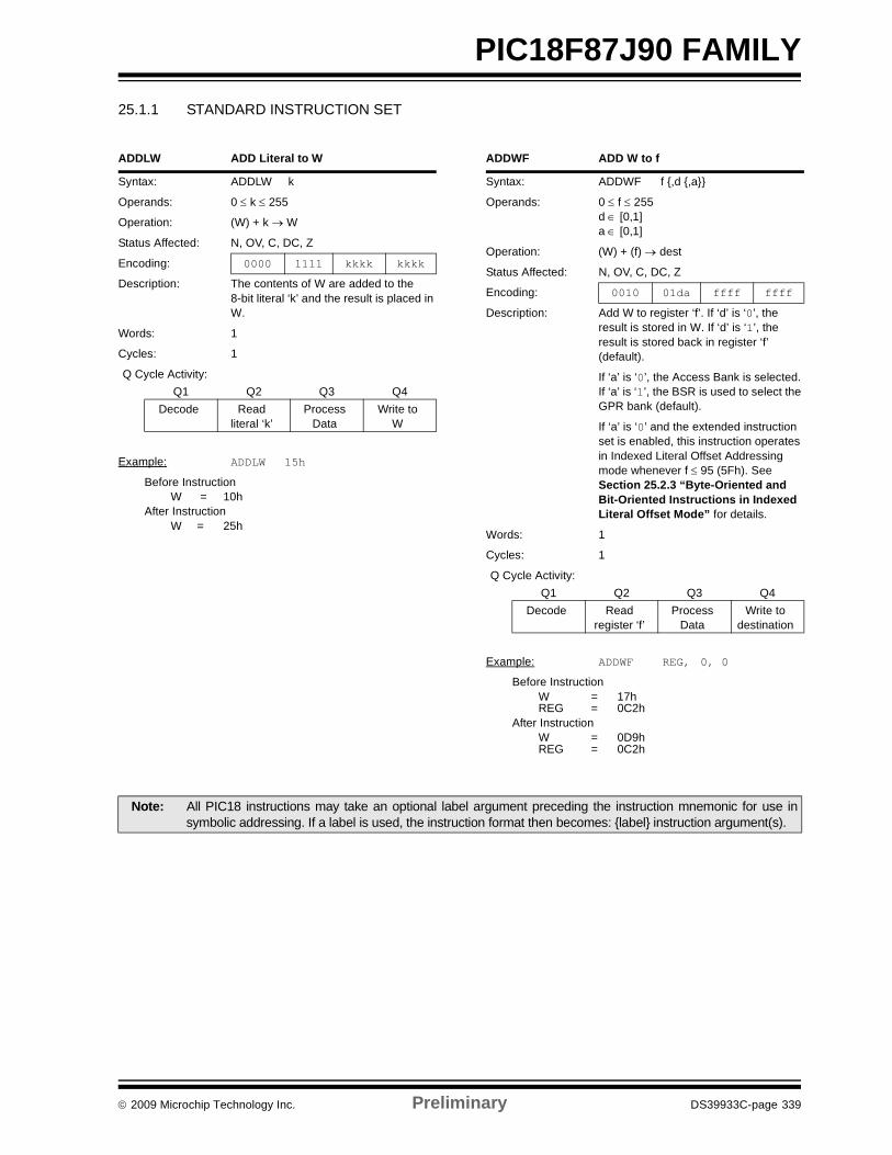
© 2009 Microchip Technology Inc. Preliminary DS39933C-page 339
PIC18F87J90 FAMILY25.1.1 STANDARD INSTRUCTION SET
ADDLW ADD Literal to W
Syntax: ADDLW k
Operands: 0 ≤ k ≤ 255
Operation: (W) + k → W
Status Affected: N, OV, C, DC, Z
Encoding: 0000 1111 kkkk kkkk
Description: The contents of W are added to the 8-bit literal ‘k’ and the result is placed in W.
Words: 1
Cycles: 1
Q Cycle Activity:Q1 Q2 Q3 Q4
Decode Readliteral ‘k’
Process Data
Write to W
Example: ADDLW 15h
Before InstructionW = 10h
After InstructionW = 25h
ADDWF ADD W to f
Syntax: ADDWF f ,d ,a
Operands: 0 ≤ f ≤ 255d ∈ [0,1]a ∈ [0,1]
Operation: (W) + (f) → dest
Status Affected: N, OV, C, DC, Z
Encoding: 0010 01da ffff ffff
Description: Add W to register ‘f’. If ‘d’ is ‘0’, the result is stored in W. If ‘d’ is ‘1’, the result is stored back in register ‘f’ (default).
If ‘a’ is ‘0’, the Access Bank is selected. If ‘a’ is ‘1’, the BSR is used to select the GPR bank (default).
If ‘a’ is ‘0’ and the extended instruction set is enabled, this instruction operates in Indexed Literal Offset Addressing mode whenever f ≤ 95 (5Fh). See Section 25.2.3 “Byte-Oriented and Bit-Oriented Instructions in Indexed Literal Offset Mode” for details.
Words: 1
Cycles: 1
Q Cycle Activity:Q1 Q2 Q3 Q4
Decode Readregister ‘f’
Process Data
Write todestination
Example: ADDWF REG, 0, 0
Before InstructionW = 17hREG = 0C2h
After InstructionW = 0D9hREG = 0C2h
Note: All PIC18 instructions may take an optional label argument preceding the instruction mnemonic for use insymbolic addressing. If a label is used, the instruction format then becomes: label instruction argument(s).
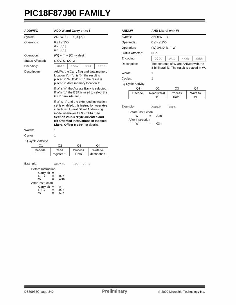
PIC18F87J90 FAMILY
DS39933C-page 340 Preliminary © 2009 Microchip Technology Inc.
ADDWFC ADD W and Carry bit to f
Syntax: ADDWFC f ,d ,a
Operands: 0 ≤ f ≤ 255d ∈ [0,1]a ∈ [0,1]
Operation: (W) + (f) + (C) → dest
Status Affected: N,OV, C, DC, Z
Encoding: 0010 00da ffff ffff
Description: Add W, the Carry flag and data memory location ‘f’. If ‘d’ is ‘0’, the result is placed in W. If ‘d’ is ‘1’, the result is placed in data memory location ‘f’.
If ‘a’ is ‘0’, the Access Bank is selected. If ‘a’ is ‘1’, the BSR is used to select the GPR bank (default).
If ‘a’ is ‘0’ and the extended instruction set is enabled, this instruction operates in Indexed Literal Offset Addressing mode whenever f ≤ 95 (5Fh). See Section 25.2.3 “Byte-Oriented and Bit-Oriented Instructions in Indexed Literal Offset Mode” for details.
Words: 1
Cycles: 1
Q Cycle Activity:Q1 Q2 Q3 Q4
Decode Readregister ‘f’
Process Data
Write to destination
Example: ADDWFC REG, 0, 1
Before InstructionCarry bit = 1REG = 02hW = 4Dh
After InstructionCarry bit = 0REG = 02hW = 50h
ANDLW AND Literal with W
Syntax: ANDLW k
Operands: 0 ≤ k ≤ 255
Operation: (W) .AND. k → W
Status Affected: N, Z
Encoding: 0000 1011 kkkk kkkk
Description: The contents of W are ANDed with the 8-bit literal ‘k’. The result is placed in W.
Words: 1
Cycles: 1
Q Cycle Activity:Q1 Q2 Q3 Q4
Decode Read literal ‘k’
Process Data
Write to W
Example: ANDLW 05Fh
Before InstructionW = A3h
After InstructionW = 03h
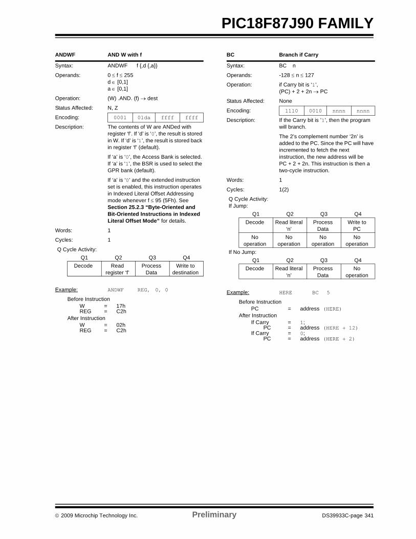
© 2009 Microchip Technology Inc. Preliminary DS39933C-page 341
PIC18F87J90 FAMILY
ANDWF AND W with f
Syntax: ANDWF f ,d ,a
Operands: 0 ≤ f ≤ 255d ∈ [0,1]a ∈ [0,1]
Operation: (W) .AND. (f) → dest
Status Affected: N, Z
Encoding: 0001 01da ffff ffff
Description: The contents of W are ANDed with register ‘f’. If ‘d’ is ‘0’, the result is stored in W. If ‘d’ is ‘1’, the result is stored back in register ‘f’ (default).
If ‘a’ is ‘0’, the Access Bank is selected. If ‘a’ is ‘1’, the BSR is used to select the GPR bank (default).
If ‘a’ is ‘0’ and the extended instruction set is enabled, this instruction operates in Indexed Literal Offset Addressing mode whenever f ≤ 95 (5Fh). See Section 25.2.3 “Byte-Oriented and Bit-Oriented Instructions in Indexed Literal Offset Mode” for details.
Words: 1
Cycles: 1
Q Cycle Activity:Q1 Q2 Q3 Q4
Decode Readregister ‘f’
Process Data
Write to destination
Example: ANDWF REG, 0, 0
Before InstructionW = 17hREG = C2h
After InstructionW = 02hREG = C2h
BC Branch if Carry
Syntax: BC n
Operands: -128 ≤ n ≤ 127
Operation: if Carry bit is ‘1’,(PC) + 2 + 2n → PC
Status Affected: None
Encoding: 1110 0010 nnnn nnnn
Description: If the Carry bit is ’1’, then the program will branch.
The 2’s complement number ‘2n’ is added to the PC. Since the PC will have incremented to fetch the next instruction, the new address will be PC + 2 + 2n. This instruction is then a two-cycle instruction.
Words: 1
Cycles: 1(2)
Q Cycle Activity:If Jump:
Q1 Q2 Q3 Q4Decode Read literal
‘n’Process
DataWrite to
PCNo
operationNo
operationNo
operationNo
operationIf No Jump:
Q1 Q2 Q3 Q4Decode Read literal
‘n’Process
DataNo
operation
Example: HERE BC 5
Before InstructionPC = address (HERE)
After InstructionIf Carry = 1;
PC = address (HERE + 12)If Carry = 0;
PC = address (HERE + 2)
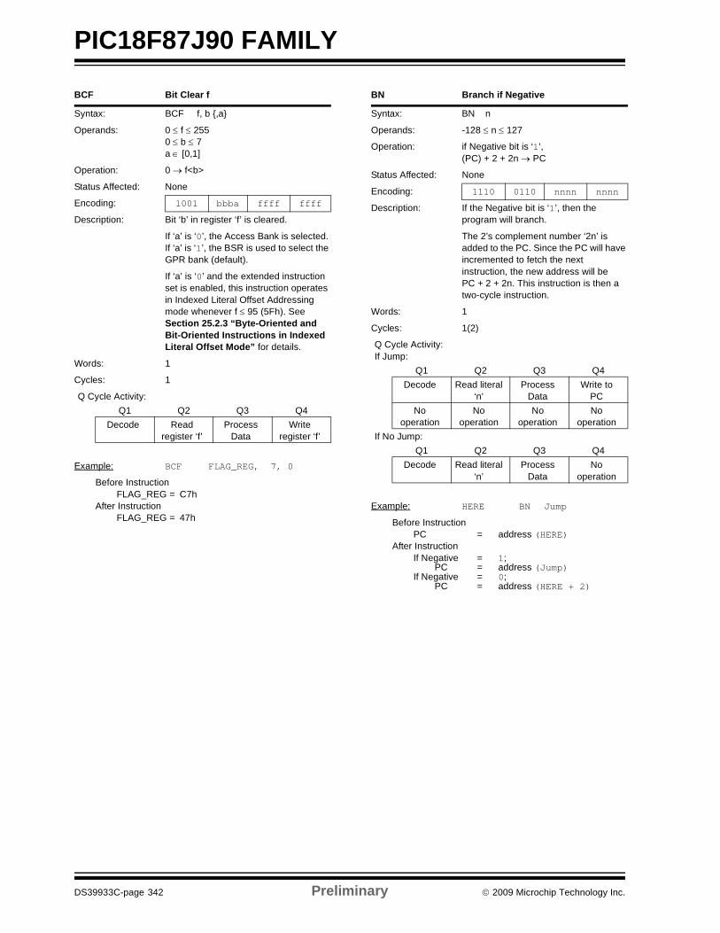
PIC18F87J90 FAMILY
DS39933C-page 342 Preliminary © 2009 Microchip Technology Inc.
BCF Bit Clear f
Syntax: BCF f, b ,a
Operands: 0 ≤ f ≤ 2550 ≤ b ≤ 7a ∈ [0,1]
Operation: 0 → f<b>
Status Affected: None
Encoding: 1001 bbba ffff ffff
Description: Bit ‘b’ in register ‘f’ is cleared.
If ‘a’ is ‘0’, the Access Bank is selected. If ‘a’ is ‘1’, the BSR is used to select the GPR bank (default).
If ‘a’ is ‘0’ and the extended instruction set is enabled, this instruction operates in Indexed Literal Offset Addressing mode whenever f ≤ 95 (5Fh). See Section 25.2.3 “Byte-Oriented and Bit-Oriented Instructions in Indexed Literal Offset Mode” for details.
Words: 1
Cycles: 1
Q Cycle Activity:Q1 Q2 Q3 Q4
Decode Readregister ‘f’
Process Data
Writeregister ‘f’
Example: BCF FLAG_REG, 7, 0
Before InstructionFLAG_REG = C7h
After InstructionFLAG_REG = 47h
BN Branch if Negative
Syntax: BN n
Operands: -128 ≤ n ≤ 127
Operation: if Negative bit is ‘1’,(PC) + 2 + 2n → PC
Status Affected: None
Encoding: 1110 0110 nnnn nnnn
Description: If the Negative bit is ‘1’, then the program will branch.
The 2’s complement number ‘2n’ is added to the PC. Since the PC will have incremented to fetch the next instruction, the new address will be PC + 2 + 2n. This instruction is then a two-cycle instruction.
Words: 1
Cycles: 1(2)
Q Cycle Activity:If Jump:
Q1 Q2 Q3 Q4Decode Read literal
‘n’Process
DataWrite to
PCNo
operationNo
operationNo
operationNo
operationIf No Jump:
Q1 Q2 Q3 Q4Decode Read literal
‘n’Process
DataNo
operation
Example: HERE BN Jump
Before InstructionPC = address (HERE)
After InstructionIf Negative = 1;
PC = address (Jump)If Negative = 0;
PC = address (HERE + 2)
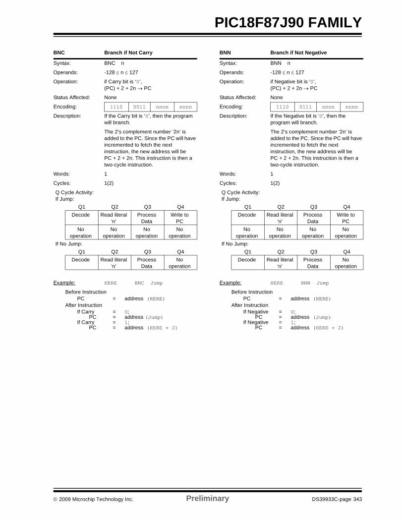
© 2009 Microchip Technology Inc. Preliminary DS39933C-page 343
PIC18F87J90 FAMILY
BNC Branch if Not Carry
Syntax: BNC n
Operands: -128 ≤ n ≤ 127
Operation: if Carry bit is ‘0’,(PC) + 2 + 2n → PC
Status Affected: None
Encoding: 1110 0011 nnnn nnnn
Description: If the Carry bit is ‘0’, then the program will branch.
The 2’s complement number ‘2n’ is added to the PC. Since the PC will have incremented to fetch the next instruction, the new address will be PC + 2 + 2n. This instruction is then a two-cycle instruction.
Words: 1
Cycles: 1(2)
Q Cycle Activity:If Jump:
Q1 Q2 Q3 Q4Decode Read literal
‘n’Process
DataWrite to
PCNo
operationNo
operationNo
operationNo
operationIf No Jump:
Q1 Q2 Q3 Q4Decode Read literal
‘n’Process
DataNo
operation
Example: HERE BNC Jump
Before InstructionPC = address (HERE)
After InstructionIf Carry = 0;
PC = address (Jump)If Carry = 1;
PC = address (HERE + 2)
BNN Branch if Not Negative
Syntax: BNN n
Operands: -128 ≤ n ≤ 127
Operation: if Negative bit is ‘0’,(PC) + 2 + 2n → PC
Status Affected: None
Encoding: 1110 0111 nnnn nnnn
Description: If the Negative bit is ‘0’, then the program will branch.
The 2’s complement number ‘2n’ is added to the PC. Since the PC will have incremented to fetch the next instruction, the new address will be PC + 2 + 2n. This instruction is then a two-cycle instruction.
Words: 1
Cycles: 1(2)
Q Cycle Activity:If Jump:
Q1 Q2 Q3 Q4Decode Read literal
‘n’Process
DataWrite to
PCNo
operationNo
operationNo
operationNo
operationIf No Jump:
Q1 Q2 Q3 Q4Decode Read literal
‘n’Process
DataNo
operation
Example: HERE BNN Jump
Before InstructionPC = address (HERE)
After InstructionIf Negative = 0;
PC = address (Jump)If Negative = 1;
PC = address (HERE + 2)
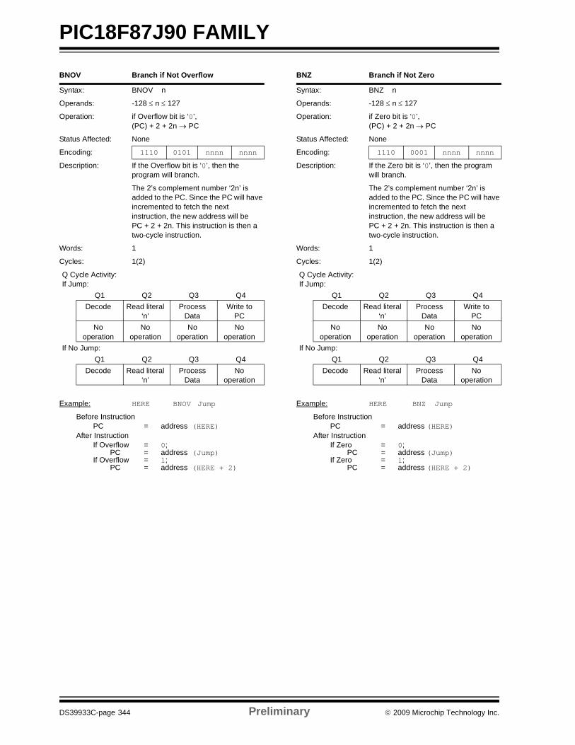
PIC18F87J90 FAMILY
DS39933C-page 344 Preliminary © 2009 Microchip Technology Inc.
BNOV Branch if Not Overflow
Syntax: BNOV n
Operands: -128 ≤ n ≤ 127
Operation: if Overflow bit is ‘0’,(PC) + 2 + 2n → PC
Status Affected: None
Encoding: 1110 0101 nnnn nnnn
Description: If the Overflow bit is ‘0’, then the program will branch.
The 2’s complement number ‘2n’ is added to the PC. Since the PC will have incremented to fetch the next instruction, the new address will be PC + 2 + 2n. This instruction is then a two-cycle instruction.
Words: 1
Cycles: 1(2)
Q Cycle Activity:If Jump:
Q1 Q2 Q3 Q4Decode Read literal
‘n’Process
DataWrite to
PCNo
operationNo
operationNo
operationNo
operationIf No Jump:
Q1 Q2 Q3 Q4Decode Read literal
‘n’Process
DataNo
operation
Example: HERE BNOV Jump
Before InstructionPC = address (HERE)
After InstructionIf Overflow = 0;
PC = address (Jump)If Overflow = 1;
PC = address (HERE + 2)
BNZ Branch if Not Zero
Syntax: BNZ n
Operands: -128 ≤ n ≤ 127
Operation: if Zero bit is ‘0’,(PC) + 2 + 2n → PC
Status Affected: None
Encoding: 1110 0001 nnnn nnnn
Description: If the Zero bit is ‘0’, then the program will branch.
The 2’s complement number ‘2n’ is added to the PC. Since the PC will have incremented to fetch the next instruction, the new address will be PC + 2 + 2n. This instruction is then a two-cycle instruction.
Words: 1
Cycles: 1(2)
Q Cycle Activity:If Jump:
Q1 Q2 Q3 Q4Decode Read literal
‘n’Process
DataWrite to
PCNo
operationNo
operationNo
operationNo
operationIf No Jump:
Q1 Q2 Q3 Q4Decode Read literal
‘n’Process
DataNo
operation
Example: HERE BNZ Jump
Before InstructionPC = address (HERE)
After InstructionIf Zero = 0;
PC = address (Jump)If Zero = 1;
PC = address (HERE + 2)
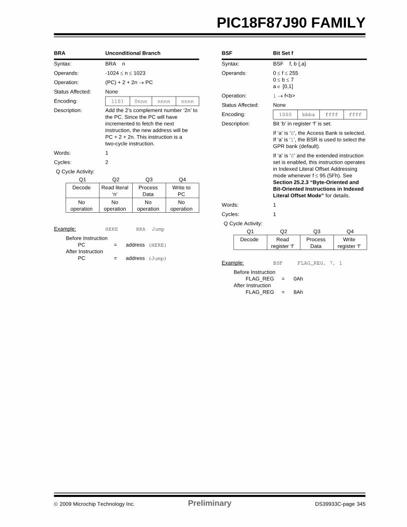
© 2009 Microchip Technology Inc. Preliminary DS39933C-page 345
PIC18F87J90 FAMILY
BRA Unconditional Branch
Syntax: BRA n
Operands: -1024 ≤ n ≤ 1023
Operation: (PC) + 2 + 2n → PC
Status Affected: None
Encoding: 1101 0nnn nnnn nnnn
Description: Add the 2’s complement number ‘2n’ to the PC. Since the PC will have incremented to fetch the next instruction, the new address will be PC + 2 + 2n. This instruction is a two-cycle instruction.
Words: 1
Cycles: 2
Q Cycle Activity:Q1 Q2 Q3 Q4
Decode Read literal ‘n’
Process Data
Write to PC
No operation
No operation
No operation
No operation
Example: HERE BRA Jump
Before InstructionPC = address (HERE)
After InstructionPC = address (Jump)
BSF Bit Set f
Syntax: BSF f, b ,a
Operands: 0 ≤ f ≤ 2550 ≤ b ≤ 7a ∈ [0,1]
Operation: 1 → f<b>
Status Affected: None
Encoding: 1000 bbba ffff ffff
Description: Bit ‘b’ in register ‘f’ is set.
If ‘a’ is ‘0’, the Access Bank is selected. If ‘a’ is ‘1’, the BSR is used to select the GPR bank (default).
If ‘a’ is ‘0’ and the extended instruction set is enabled, this instruction operates in Indexed Literal Offset Addressing mode whenever f ≤ 95 (5Fh). See Section 25.2.3 “Byte-Oriented and Bit-Oriented Instructions in Indexed Literal Offset Mode” for details.
Words: 1
Cycles: 1
Q Cycle Activity:Q1 Q2 Q3 Q4
Decode Readregister ‘f’
Process Data
Writeregister ‘f’
Example: BSF FLAG_REG, 7, 1
Before InstructionFLAG_REG = 0Ah
After InstructionFLAG_REG = 8Ah
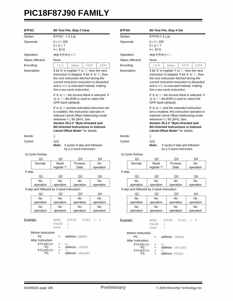
PIC18F87J90 FAMILY
DS39933C-page 346 Preliminary © 2009 Microchip Technology Inc.
BTFSC Bit Test File, Skip if Clear
Syntax: BTFSC f, b ,a
Operands: 0 ≤ f ≤ 2550 ≤ b ≤ 7a ∈ [0,1]
Operation: skip if (f<b>) = 0
Status Affected: None
Encoding: 1011 bbba ffff ffff
Description: If bit ‘b’ in register ‘f’ is ‘0’, then the next instruction is skipped. If bit ‘b’ is ‘0’, then the next instruction fetched during the current instruction execution is discarded and a NOP is executed instead, making this a two-cycle instruction.
If ‘a’ is ‘0’, the Access Bank is selected. If ‘a’ is ‘1’, the BSR is used to select the GPR bank (default).
If ‘a’ is ‘0’ and the extended instruction set is enabled, this instruction operates in Indexed Literal Offset Addressing mode whenever f ≤ 95 (5Fh). See Section 25.2.3 “Byte-Oriented and Bit-Oriented Instructions in Indexed Literal Offset Mode” for details.
Words: 1
Cycles: 1(2)Note: 3 cycles if skip and followed
by a 2-word instruction.
Q Cycle Activity:Q1 Q2 Q3 Q4
Decode Readregister ‘f’
Process Data
No operation
If skip:Q1 Q2 Q3 Q4No
operationNo
operationNo
operationNo
operationIf skip and followed by 2-word instruction:
Q1 Q2 Q3 Q4No
operationNo
operationNo
operationNo
operationNo
operationNo
operationNo
operationNo
operation
Example: HEREFALSETRUE
BTFSC::
FLAG, 1, 0
Before InstructionPC = address (HERE)
After InstructionIf FLAG<1> = 0;
PC = address (TRUE)If FLAG<1> = 1;
PC = address (FALSE)
BTFSS Bit Test File, Skip if Set
Syntax: BTFSS f, b ,a
Operands: 0 ≤ f ≤ 2550 ≤ b < 7a ∈ [0,1]
Operation: skip if (f<b>) = 1
Status Affected: None
Encoding: 1010 bbba ffff ffff
Description: If bit ‘b’ in register ‘f’ is ‘1’, then the next instruction is skipped. If bit ‘b’ is ‘1’, then the next instruction fetched during the current instruction execution is discarded and a NOP is executed instead, making this a two-cycle instruction.
If ‘a’ is ‘0’, the Access Bank is selected. If ‘a’ is ‘1’, the BSR is used to select the GPR bank (default).
If ‘a’ is ‘0’ and the extended instruction set is enabled, this instruction operates in Indexed Literal Offset Addressing mode whenever f ≤ 95 (5Fh). See Section 25.2.3 “Byte-Oriented and Bit-Oriented Instructions in Indexed Literal Offset Mode” for details.
Words: 1
Cycles: 1(2)Note: 3 cycles if skip and followed
by a 2-word instruction.
Q Cycle Activity:Q1 Q2 Q3 Q4
Decode Readregister ‘f’
Process Data
No operation
If skip:Q1 Q2 Q3 Q4No
operationNo
operationNo
operationNo
operationIf skip and followed by 2-word instruction:
Q1 Q2 Q3 Q4No
operationNo
operationNo
operationNo
operationNo
operationNo
operationNo
operationNo
operation
Example: HEREFALSETRUE
BTFSS::
FLAG, 1, 0
Before InstructionPC = address (HERE)
After InstructionIf FLAG<1> = 0;
PC = address (FALSE)If FLAG<1> = 1;
PC = address (TRUE)
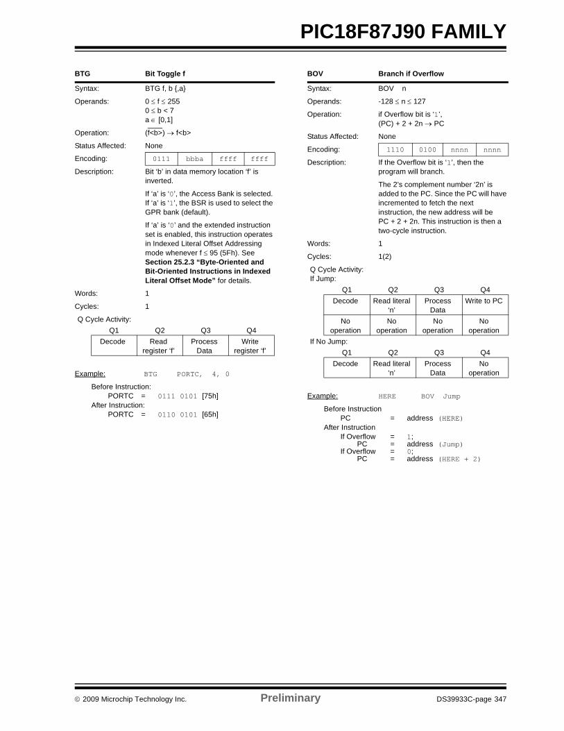
© 2009 Microchip Technology Inc. Preliminary DS39933C-page 347
PIC18F87J90 FAMILY
BTG Bit Toggle f
Syntax: BTG f, b ,a
Operands: 0 ≤ f ≤ 2550 ≤ b < 7a ∈ [0,1]
Operation: (f<b>) → f<b>
Status Affected: None
Encoding: 0111 bbba ffff ffff
Description: Bit ‘b’ in data memory location ‘f’ is inverted.
If ‘a’ is ‘0’, the Access Bank is selected. If ‘a’ is ‘1’, the BSR is used to select the GPR bank (default).
If ‘a’ is ‘0’ and the extended instruction set is enabled, this instruction operates in Indexed Literal Offset Addressing mode whenever f ≤ 95 (5Fh). See Section 25.2.3 “Byte-Oriented and Bit-Oriented Instructions in Indexed Literal Offset Mode” for details.
Words: 1
Cycles: 1
Q Cycle Activity:Q1 Q2 Q3 Q4
Decode Readregister ‘f’
Process Data
Writeregister ‘f’
Example: BTG PORTC, 4, 0
Before Instruction:PORTC = 0111 0101 [75h]
After Instruction:PORTC = 0110 0101 [65h]
BOV Branch if Overflow
Syntax: BOV n
Operands: -128 ≤ n ≤ 127
Operation: if Overflow bit is ‘1’,(PC) + 2 + 2n → PC
Status Affected: None
Encoding: 1110 0100 nnnn nnnn
Description: If the Overflow bit is ‘1’, then the program will branch.
The 2’s complement number ‘2n’ is added to the PC. Since the PC will have incremented to fetch the next instruction, the new address will be PC + 2 + 2n. This instruction is then a two-cycle instruction.
Words: 1
Cycles: 1(2)
Q Cycle Activity:If Jump:
Q1 Q2 Q3 Q4Decode Read literal
‘n’Process
DataWrite to PC
No operation
No operation
No operation
No operation
If No Jump:Q1 Q2 Q3 Q4
Decode Read literal ‘n’
Process Data
No operation
Example: HERE BOV Jump
Before InstructionPC = address (HERE)
After InstructionIf Overflow = 1;
PC = address (Jump)If Overflow = 0;
PC = address (HERE + 2)
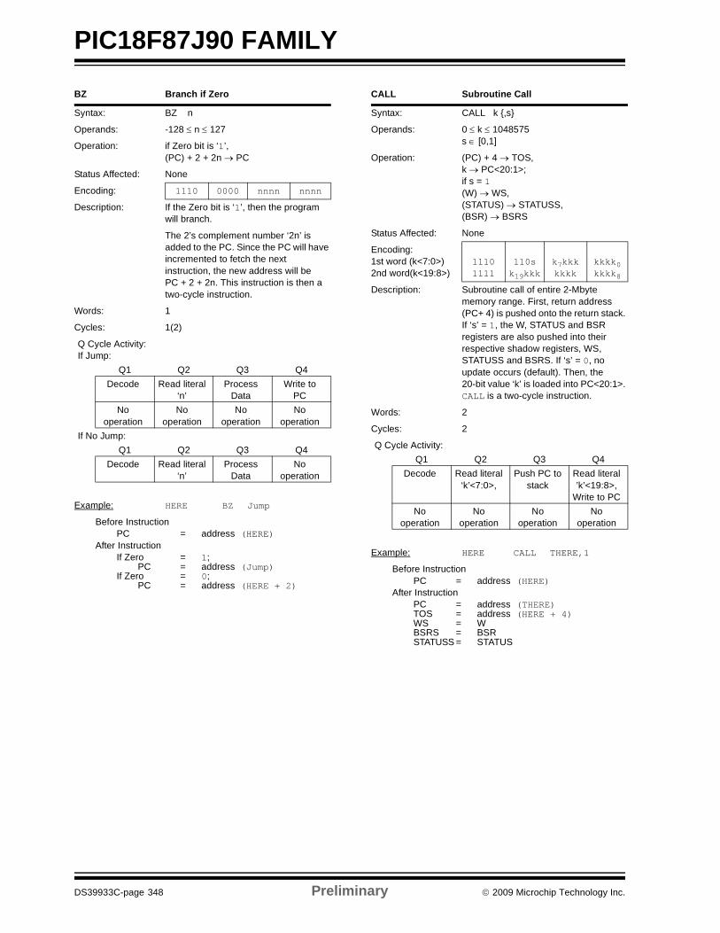
PIC18F87J90 FAMILY
DS39933C-page 348 Preliminary © 2009 Microchip Technology Inc.
BZ Branch if Zero
Syntax: BZ n
Operands: -128 ≤ n ≤ 127
Operation: if Zero bit is ‘1’,(PC) + 2 + 2n → PC
Status Affected: None
Encoding: 1110 0000 nnnn nnnn
Description: If the Zero bit is ‘1’, then the program will branch.
The 2’s complement number ‘2n’ is added to the PC. Since the PC will have incremented to fetch the next instruction, the new address will be PC + 2 + 2n. This instruction is then a two-cycle instruction.
Words: 1
Cycles: 1(2)
Q Cycle Activity:If Jump:
Q1 Q2 Q3 Q4Decode Read literal
‘n’Process
DataWrite to
PCNo
operationNo
operationNo
operationNo
operationIf No Jump:
Q1 Q2 Q3 Q4Decode Read literal
‘n’Process
DataNo
operation
Example: HERE BZ Jump
Before InstructionPC = address (HERE)
After InstructionIf Zero = 1;
PC = address (Jump)If Zero = 0;
PC = address (HERE + 2)
CALL Subroutine Call
Syntax: CALL k ,s
Operands: 0 ≤ k ≤ 1048575s ∈ [0,1]
Operation: (PC) + 4 → TOS,k → PC<20:1>;if s = 1(W) → WS,(STATUS) → STATUSS,(BSR) → BSRS
Status Affected: None
Encoding:1st word (k<7:0>)2nd word(k<19:8>)
11101111
110sk19kkk
k7kkkkkkk
kkkk0kkkk8
Description: Subroutine call of entire 2-Mbyte memory range. First, return address (PC+ 4) is pushed onto the return stack. If ‘s’ = 1, the W, STATUS and BSR registers are also pushed into their respective shadow registers, WS, STATUSS and BSRS. If ‘s’ = 0, no update occurs (default). Then, the 20-bit value ‘k’ is loaded into PC<20:1>. CALL is a two-cycle instruction.
Words: 2
Cycles: 2
Q Cycle Activity:Q1 Q2 Q3 Q4
Decode Read literal ‘k’<7:0>,
Push PC to stack
Read literal ’k’<19:8>,
Write to PCNo
operationNo
operationNo
operationNo
operation
Example: HERE CALL THERE,1
Before InstructionPC = address (HERE)
After InstructionPC = address (THERE)TOS = address (HERE + 4)WS = WBSRS = BSRSTATUSS = STATUS
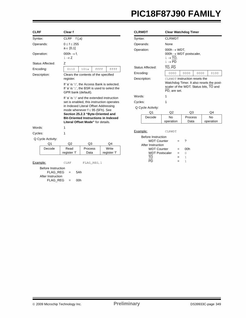
© 2009 Microchip Technology Inc. Preliminary DS39933C-page 349
PIC18F87J90 FAMILY
CLRF Clear f
Syntax: CLRF f ,a
Operands: 0 ≤ f ≤ 255a ∈ [0,1]
Operation: 000h → f,1 → Z
Status Affected: Z
Encoding: 0110 101a ffff ffff
Description: Clears the contents of the specified register.
If ‘a’ is ‘0’, the Access Bank is selected. If ‘a’ is ‘1’, the BSR is used to select the GPR bank (default).
If ‘a’ is ‘0’ and the extended instruction set is enabled, this instruction operates in Indexed Literal Offset Addressing mode whenever f ≤ 95 (5Fh). See Section 25.2.3 “Byte-Oriented and Bit-Oriented Instructions in Indexed Literal Offset Mode” for details.
Words: 1
Cycles: 1
Q Cycle Activity:Q1 Q2 Q3 Q4
Decode Readregister ‘f’
Process Data
Writeregister ‘f’
Example: CLRF FLAG_REG,1
Before InstructionFLAG_REG = 5Ah
After InstructionFLAG_REG = 00h
CLRWDT Clear Watchdog Timer
Syntax: CLRWDT
Operands: None
Operation: 000h → WDT,000h → WDT postscaler,1 → TO,1 → PD
Status Affected: TO, PD
Encoding: 0000 0000 0000 0100
Description: CLRWDT instruction resets the Watchdog Timer. It also resets the post-scaler of the WDT. Status bits, TO and PD, are set.
Words: 1
Cycles: 1
Q Cycle Activity:Q1 Q2 Q3 Q4
Decode No operation
Process Data
No operation
Example: CLRWDT
Before InstructionWDT Counter = ?
After InstructionWDT Counter = 00hWDT Postscaler = 0TO = 1PD = 1
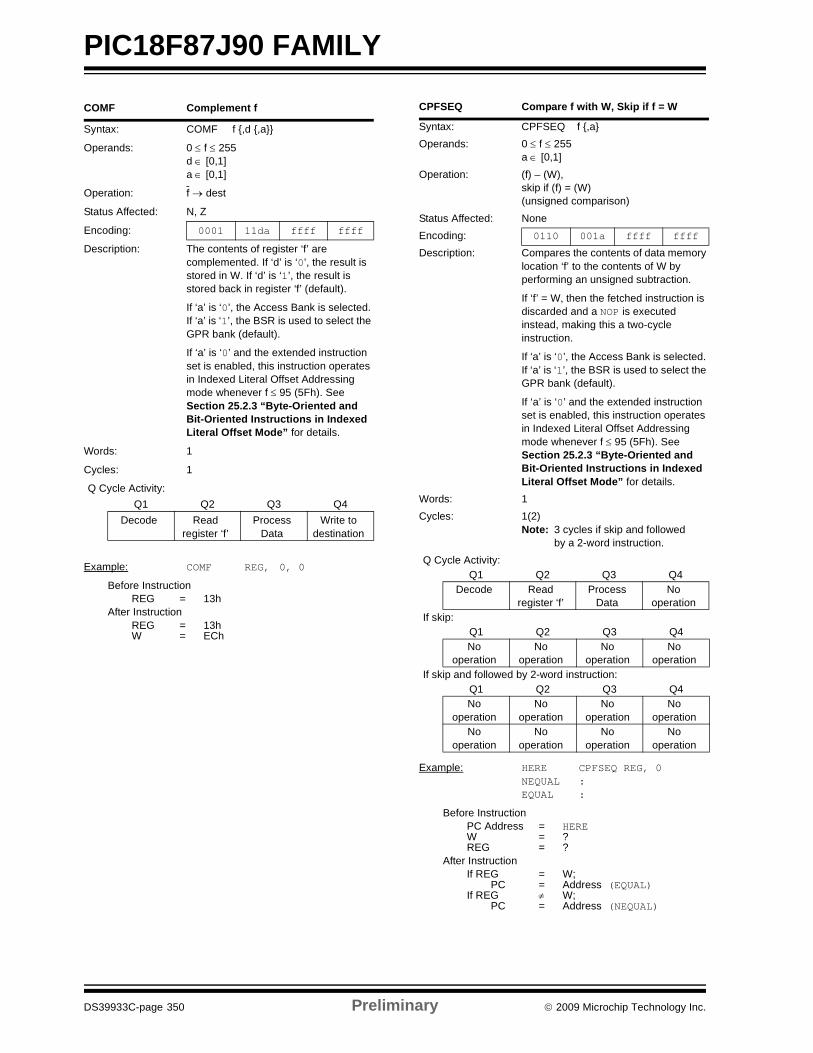
PIC18F87J90 FAMILY
DS39933C-page 350 Preliminary © 2009 Microchip Technology Inc.
COMF Complement f
Syntax: COMF f ,d ,a
Operands: 0 ≤ f ≤ 255d ∈ [0,1]a ∈ [0,1]
Operation: f → dest
Status Affected: N, Z
Encoding: 0001 11da ffff ffff
Description: The contents of register ‘f’ are complemented. If ‘d’ is ‘0’, the result is stored in W. If ‘d’ is ‘1’, the result is stored back in register ‘f’ (default).
If ‘a’ is ‘0’, the Access Bank is selected. If ‘a’ is ‘1’, the BSR is used to select the GPR bank (default).
If ‘a’ is ‘0’ and the extended instruction set is enabled, this instruction operates in Indexed Literal Offset Addressing mode whenever f ≤ 95 (5Fh). See Section 25.2.3 “Byte-Oriented and Bit-Oriented Instructions in Indexed Literal Offset Mode” for details.
Words: 1
Cycles: 1
Q Cycle Activity:Q1 Q2 Q3 Q4
Decode Readregister ‘f’
Process Data
Write todestination
Example: COMF REG, 0, 0
Before InstructionREG = 13h
After InstructionREG = 13hW = ECh
CPFSEQ Compare f with W, Skip if f = W
Syntax: CPFSEQ f ,aOperands: 0 ≤ f ≤ 255
a ∈ [0,1]Operation: (f) – (W),
skip if (f) = (W) (unsigned comparison)
Status Affected: NoneEncoding: 0110 001a ffff ffff
Description: Compares the contents of data memory location ‘f’ to the contents of W by performing an unsigned subtraction.
If ‘f’ = W, then the fetched instruction is discarded and a NOP is executed instead, making this a two-cycle instruction.
If ‘a’ is ‘0’, the Access Bank is selected. If ‘a’ is ‘1’, the BSR is used to select the GPR bank (default).
If ‘a’ is ‘0’ and the extended instruction set is enabled, this instruction operates in Indexed Literal Offset Addressing mode whenever f ≤ 95 (5Fh). See Section 25.2.3 “Byte-Oriented and Bit-Oriented Instructions in Indexed Literal Offset Mode” for details.
Words: 1Cycles: 1(2)
Note: 3 cycles if skip and followedby a 2-word instruction.
Q Cycle Activity:Q1 Q2 Q3 Q4
Decode Readregister ‘f’
Process Data
No operation
If skip:Q1 Q2 Q3 Q4No
operationNo
operationNo
operationNo
operationIf skip and followed by 2-word instruction:
Q1 Q2 Q3 Q4No
operationNo
operationNo
operationNo
operationNo
operationNo
operationNo
operationNo
operation
Example: HERE CPFSEQ REG, 0NEQUAL :EQUAL :
Before InstructionPC Address = HEREW = ?REG = ?
After InstructionIf REG = W;
PC = Address (EQUAL)If REG ≠ W;
PC = Address (NEQUAL)
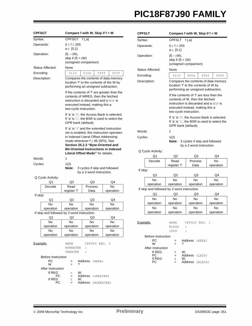
© 2009 Microchip Technology Inc. Preliminary DS39933C-page 351
PIC18F87J90 FAMILY
CPFSGT Compare f with W, Skip if f > W
Syntax: CPFSGT f ,aOperands: 0 ≤ f ≤ 255
a ∈ [0,1]Operation: (f) – (W),
skip if (f) > (W) (unsigned comparison)
Status Affected: NoneEncoding: 0110 010a ffff ffff
Description: Compares the contents of data memory location ‘f’ to the contents of the W by performing an unsigned subtraction.
If the contents of ‘f’ are greater than the contents of WREG, then the fetched instruction is discarded and a NOP is executed instead, making this a two-cycle instruction.
If ‘a’ is ‘0’, the Access Bank is selected. If ‘a’ is ‘1’, the BSR is used to select the GPR bank (default).
If ‘a’ is ‘0’ and the extended instruction set is enabled, this instruction operates in Indexed Literal Offset Addressing mode whenever f ≤ 95 (5Fh). See Section 25.2.3 “Byte-Oriented and Bit-Oriented Instructions in Indexed Literal Offset Mode” for details.
Words: 1Cycles: 1(2)
Note: 3 cycles if skip and followedby a 2-word instruction.
Q Cycle Activity:Q1 Q2 Q3 Q4
Decode Readregister ‘f’
Process Data
No operation
If skip:Q1 Q2 Q3 Q4No
operationNo
operationNo
operationNo
operationIf skip and followed by 2-word instruction:
Q1 Q2 Q3 Q4No
operationNo
operationNo
operationNo
operationNo
operationNo
operationNo
operationNo
operation
Example: HERE CPFSGT REG, 0NGREATER :GREATER :
Before InstructionPC = Address (HERE)W = ?
After InstructionIf REG > W;
PC = Address (GREATER)If REG ≤ W;
PC = Address (NGREATER)
CPFSLT Compare f with W, Skip if f < W
Syntax: CPFSLT f ,a
Operands: 0 ≤ f ≤ 255a ∈ [0,1]
Operation: (f) – (W),skip if (f) < (W) (unsigned comparison)
Status Affected: None
Encoding: 0110 000a ffff ffff
Description: Compares the contents of data memory location ‘f’ to the contents of W by performing an unsigned subtraction.
If the contents of ‘f’ are less than the contents of W, then the fetched instruction is discarded and a NOP is executed instead, making this a two-cycle instruction.
If ‘a’ is ‘0’, the Access Bank is selected. If ‘a’ is ‘1’, the BSR is used to select the GPR bank (default).
Words: 1
Cycles: 1(2)Note: 3 cycles if skip and followed
by a 2-word instruction.
Q Cycle Activity:Q1 Q2 Q3 Q4
Decode Readregister ‘f’
Process Data
No operation
If skip:Q1 Q2 Q3 Q4No
operationNo
operationNo
operationNo
operationIf skip and followed by 2-word instruction:
Q1 Q2 Q3 Q4No
operationNo
operationNo
operationNo
operationNo
operationNo
operationNo
operationNo
operation
Example: HERE CPFSLT REG, 1NLESS :LESS :
Before InstructionPC = Address (HERE)W = ?
After InstructionIf REG < W;PC = Address (LESS)If REG ≥ W;PC = Address (NLESS)
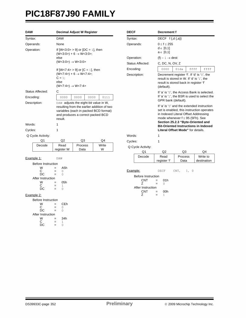
PIC18F87J90 FAMILY
DS39933C-page 352 Preliminary © 2009 Microchip Technology Inc.
DAW Decimal Adjust W Register
Syntax: DAW
Operands: None
Operation: If [W<3:0> > 9] or [DC = 1], then(W<3:0>) + 6 → W<3:0>;else (W<3:0>) → W<3:0>
If [W<7:4> > 9] or [C = 1], then(W<7:4>) + 6 → W<7:4>;C = 1;else (W<7:4>) → W<7:4>
Status Affected: C
Encoding: 0000 0000 0000 0111
Description: DAW adjusts the eight-bit value in W, resulting from the earlier addition of two variables (each in packed BCD format) and produces a correct packed BCD result.
Words: 1
Cycles: 1
Q Cycle Activity:Q1 Q2 Q3 Q4
Decode Readregister W
Process Data
WriteW
Example 1: DAW
Before InstructionW = A5hC = 0DC = 0
After InstructionW = 05hC = 1DC = 0
Example 2:Before Instruction
W = CEhC = 0DC = 0
After InstructionW = 34hC = 1DC = 0
DECF Decrement f
Syntax: DECF f ,d ,a
Operands: 0 ≤ f ≤ 255d ∈ [0,1]a ∈ [0,1]
Operation: (f) – 1 → dest
Status Affected: C, DC, N, OV, Z
Encoding: 0000 01da ffff ffff
Description: Decrement register ‘f’. If ‘d’ is ‘0’, the result is stored in W. If ‘d’ is ‘1’, the result is stored back in register ‘f’ (default).
If ‘a’ is ‘0’, the Access Bank is selected. If ‘a’ is ‘1’, the BSR is used to select the GPR bank (default).
If ‘a’ is ‘0’ and the extended instruction set is enabled, this instruction operates in Indexed Literal Offset Addressing mode whenever f ≤ 95 (5Fh). See Section 25.2.3 “Byte-Oriented and Bit-Oriented Instructions in Indexed Literal Offset Mode” for details.
Words: 1
Cycles: 1
Q Cycle Activity:Q1 Q2 Q3 Q4
Decode Readregister ‘f’
Process Data
Write to destination
Example: DECF CNT, 1, 0
Before InstructionCNT = 01hZ = 0
After InstructionCNT = 00hZ = 1
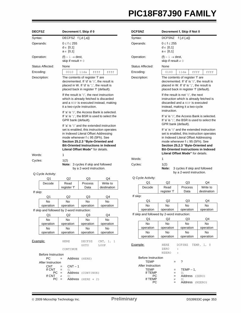
© 2009 Microchip Technology Inc. Preliminary DS39933C-page 353
PIC18F87J90 FAMILY
DECFSZ Decrement f, Skip if 0
Syntax: DECFSZ f ,d ,a
Operands: 0 ≤ f ≤ 255d ∈ [0,1]a ∈ [0,1]
Operation: (f) – 1 → dest,skip if result = 0
Status Affected: None
Encoding: 0010 11da ffff ffff
Description: The contents of register ‘f’ are decremented. If ‘d’ is ‘0’, the result is placed in W. If ‘d’ is ‘1’, the result is placed back in register ‘f’ (default).
If the result is ‘0’, the next instruction which is already fetched is discarded and a NOP is executed instead, making it a two-cycle instruction.
If ‘a’ is ‘0’, the Access Bank is selected. If ‘a’ is ‘1’, the BSR is used to select the GPR bank (default).
If ‘a’ is ‘0’ and the extended instruction set is enabled, this instruction operates in Indexed Literal Offset Addressing mode whenever f ≤ 95 (5Fh). See Section 25.2.3 “Byte-Oriented and Bit-Oriented Instructions in Indexed Literal Offset Mode” for details.
Words: 1
Cycles: 1(2)Note: 3 cycles if skip and followed
by a 2-word instruction.
Q Cycle Activity:Q1 Q2 Q3 Q4
Decode Readregister ‘f’
Process Data
Write to destination
If skip:Q1 Q2 Q3 Q4No
operationNo
operationNo
operationNo
operationIf skip and followed by 2-word instruction:
Q1 Q2 Q3 Q4No
operationNo
operationNo
operationNo
operationNo
operationNo
operationNo
operationNo
operation
Example: HERE DECFSZ CNT, 1, 1 GOTO LOOPCONTINUE
Before InstructionPC = Address (HERE)
After InstructionCNT = CNT – 1If CNT = 0;
PC = Address (CONTINUE)If CNT ≠ 0;
PC = Address (HERE + 2)
DCFSNZ Decrement f, Skip if Not 0
Syntax: DCFSNZ f ,d ,a
Operands: 0 ≤ f ≤ 255d ∈ [0,1]a ∈ [0,1]
Operation: (f) – 1 → dest,skip if result ≠ 0
Status Affected: None
Encoding: 0100 11da ffff ffff
Description: The contents of register ‘f’ are decremented. If ‘d’ is ‘0’, the result is placed in W. If ‘d’ is ‘1’, the result is placed back in register ‘f’ (default).
If the result is not ‘0’, the next instruction which is already fetched is discarded and a NOP is executed instead, making it a two-cycle instruction.
If ‘a’ is ‘0’, the Access Bank is selected. If ‘a’ is ‘1’, the BSR is used to select the GPR bank (default).
If ‘a’ is ‘0’ and the extended instruction set is enabled, this instruction operates in Indexed Literal Offset Addressing mode whenever f ≤ 95 (5Fh). See Section 25.2.3 “Byte-Oriented and Bit-Oriented Instructions in Indexed Literal Offset Mode” for details.
Words: 1
Cycles: 1(2)Note: 3 cycles if skip and followed
by a 2-word instruction.
Q Cycle Activity:Q1 Q2 Q3 Q4
Decode Readregister ‘f’
Process Data
Write to destination
If skip:Q1 Q2 Q3 Q4No
operationNo
operationNo
operationNo
operationIf skip and followed by 2-word instruction:
Q1 Q2 Q3 Q4No
operationNo
operationNo
operationNo
operationNo
operationNo
operationNo
operationNo
operation
Example: HERE DCFSNZ TEMP, 1, 0ZERO : NZERO :
Before InstructionTEMP = ?
After InstructionTEMP = TEMP – 1,If TEMP = 0;
PC = Address (ZERO)If TEMP ≠ 0;
PC = Address (NZERO)
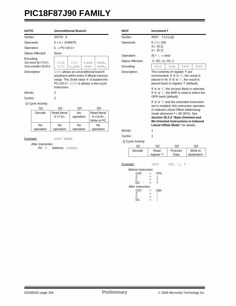
PIC18F87J90 FAMILY
DS39933C-page 354 Preliminary © 2009 Microchip Technology Inc.
GOTO Unconditional Branch
Syntax: GOTO k
Operands: 0 ≤ k ≤ 1048575
Operation: k → PC<20:1>
Status Affected: None
Encoding:1st word (k<7:0>)2nd word(k<19:8>)
11101111
1111k19kkk
k7kkkkkkk
kkkk0kkkk8
Description: GOTO allows an unconditional branch anywhere within entire 2-Mbyte memory range. The 20-bit value ‘k’ is loaded into PC<20:1>. GOTO is always a two-cycle instruction.
Words: 2
Cycles: 2
Q Cycle Activity:Q1 Q2 Q3 Q4
Decode Read literal ‘k’<7:0>,
No operation
Read literal ‘k’<19:8>,
Write to PCNo
operationNo
operationNo
operationNo
operation
Example: GOTO THERE
After InstructionPC = Address (THERE)
INCF Increment f
Syntax: INCF f ,d ,a
Operands: 0 ≤ f ≤ 255d ∈ [0,1]a ∈ [0,1]
Operation: (f) + 1 → dest
Status Affected: C, DC, N, OV, Z
Encoding: 0010 10da ffff ffff
Description: The contents of register ‘f’ are incremented. If ‘d’ is ‘0’, the result is placed in W. If ‘d’ is ‘1’, the result is placed back in register ‘f’ (default).
If ‘a’ is ‘0’, the Access Bank is selected. If ‘a’ is ‘1’, the BSR is used to select the GPR bank (default).
If ‘a’ is ‘0’ and the extended instruction set is enabled, this instruction operates in Indexed Literal Offset Addressing mode whenever f ≤ 95 (5Fh). See Section 25.2.3 “Byte-Oriented and Bit-Oriented Instructions in Indexed Literal Offset Mode” for details.
Words: 1
Cycles: 1
Q Cycle Activity:Q1 Q2 Q3 Q4
Decode Readregister ‘f’
Process Data
Write to destination
Example: INCF CNT, 1, 0
Before InstructionCNT = FFhZ = 0C = ?DC = ?
After InstructionCNT = 00hZ = 1C = 1DC = 1
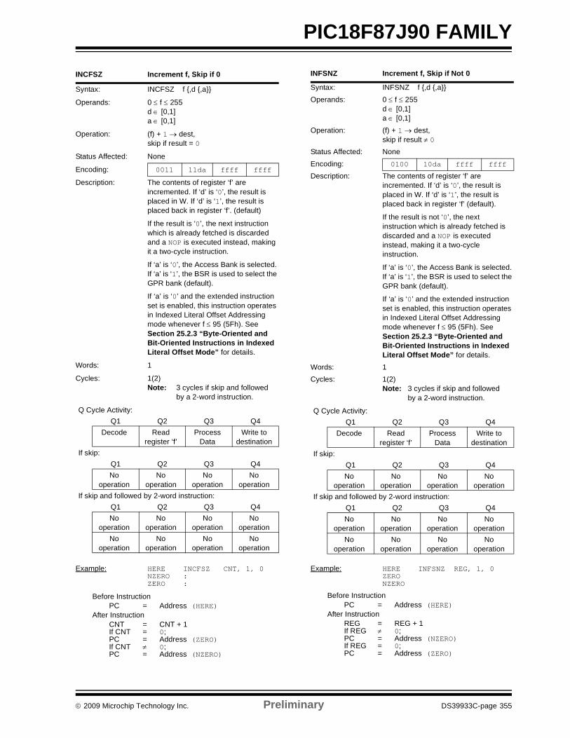
© 2009 Microchip Technology Inc. Preliminary DS39933C-page 355
PIC18F87J90 FAMILY
INCFSZ Increment f, Skip if 0
Syntax: INCFSZ f ,d ,a
Operands: 0 ≤ f ≤ 255d ∈ [0,1]a ∈ [0,1]
Operation: (f) + 1 → dest,skip if result = 0
Status Affected: None
Encoding: 0011 11da ffff ffff
Description: The contents of register ‘f’ are incremented. If ‘d’ is ‘0’, the result is placed in W. If ‘d’ is ‘1’, the result is placed back in register ‘f’. (default)
If the result is ‘0’, the next instruction which is already fetched is discarded and a NOP is executed instead, making it a two-cycle instruction.
If ‘a’ is ‘0’, the Access Bank is selected. If ‘a’ is ‘1’, the BSR is used to select the GPR bank (default).
If ‘a’ is ‘0’ and the extended instruction set is enabled, this instruction operates in Indexed Literal Offset Addressing mode whenever f ≤ 95 (5Fh). See Section 25.2.3 “Byte-Oriented and Bit-Oriented Instructions in Indexed Literal Offset Mode” for details.
Words: 1
Cycles: 1(2)Note: 3 cycles if skip and followed
by a 2-word instruction.
Q Cycle Activity:Q1 Q2 Q3 Q4
Decode Readregister ‘f’
Process Data
Write to destination
If skip:Q1 Q2 Q3 Q4No
operationNo
operationNo
operationNo
operationIf skip and followed by 2-word instruction:
Q1 Q2 Q3 Q4No
operationNo
operationNo
operationNo
operationNo
operationNo
operationNo
operationNo
operation
Example: HERE INCFSZ CNT, 1, 0NZERO : ZERO :
Before InstructionPC = Address (HERE)
After InstructionCNT = CNT + 1If CNT = 0;PC = Address (ZERO)If CNT ≠ 0;PC = Address (NZERO)
INFSNZ Increment f, Skip if Not 0
Syntax: INFSNZ f ,d ,aOperands: 0 ≤ f ≤ 255
d ∈ [0,1]a ∈ [0,1]
Operation: (f) + 1 → dest, skip if result ≠ 0
Status Affected: NoneEncoding: 0100 10da ffff ffff
Description: The contents of register ‘f’ are incremented. If ‘d’ is ‘0’, the result is placed in W. If ‘d’ is ‘1’, the result is placed back in register ‘f’ (default).
If the result is not ‘0’, the next instruction which is already fetched is discarded and a NOP is executed instead, making it a two-cycle instruction.
If ‘a’ is ‘0’, the Access Bank is selected. If ‘a’ is ‘1’, the BSR is used to select the GPR bank (default).
If ‘a’ is ‘0’ and the extended instruction set is enabled, this instruction operates in Indexed Literal Offset Addressing mode whenever f ≤ 95 (5Fh). See Section 25.2.3 “Byte-Oriented and Bit-Oriented Instructions in Indexed Literal Offset Mode” for details.
Words: 1Cycles: 1(2)
Note: 3 cycles if skip and followedby a 2-word instruction.
Q Cycle Activity:Q1 Q2 Q3 Q4
Decode Readregister ‘f’
Process Data
Write to destination
If skip:Q1 Q2 Q3 Q4No
operationNo
operationNo
operationNo
operationIf skip and followed by 2-word instruction:
Q1 Q2 Q3 Q4No
operationNo
operationNo
operationNo
operationNo
operationNo
operationNo
operationNo
operation
Example: HERE INFSNZ REG, 1, 0ZERONZERO
Before InstructionPC = Address (HERE)
After InstructionREG = REG + 1If REG ≠ 0;PC = Address (NZERO)If REG = 0;PC = Address (ZERO)
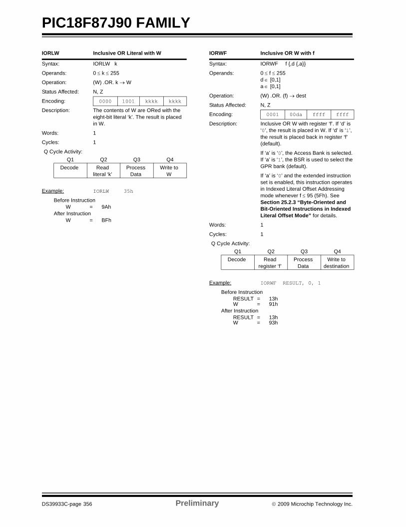
PIC18F87J90 FAMILY
DS39933C-page 356 Preliminary © 2009 Microchip Technology Inc.
IORLW Inclusive OR Literal with W
Syntax: IORLW k
Operands: 0 ≤ k ≤ 255
Operation: (W) .OR. k → W
Status Affected: N, Z
Encoding: 0000 1001 kkkk kkkk
Description: The contents of W are ORed with the eight-bit literal ‘k’. The result is placed in W.
Words: 1
Cycles: 1
Q Cycle Activity:Q1 Q2 Q3 Q4
Decode Read literal ‘k’
Process Data
Write to W
Example: IORLW 35h
Before InstructionW = 9Ah
After InstructionW = BFh
IORWF Inclusive OR W with f
Syntax: IORWF f ,d ,a
Operands: 0 ≤ f ≤ 255d ∈ [0,1]a ∈ [0,1]
Operation: (W) .OR. (f) → dest
Status Affected: N, Z
Encoding: 0001 00da ffff ffff
Description: Inclusive OR W with register ‘f’. If ‘d’ is ‘0’, the result is placed in W. If ‘d’ is ‘1’, the result is placed back in register ‘f’ (default).
If ‘a’ is ‘0’, the Access Bank is selected. If ‘a’ is ‘1’, the BSR is used to select the GPR bank (default).
If ‘a’ is ‘0’ and the extended instruction set is enabled, this instruction operates in Indexed Literal Offset Addressing mode whenever f ≤ 95 (5Fh). See Section 25.2.3 “Byte-Oriented and Bit-Oriented Instructions in Indexed Literal Offset Mode” for details.
Words: 1
Cycles: 1
Q Cycle Activity:Q1 Q2 Q3 Q4
Decode Readregister ‘f’
Process Data
Write to destination
Example: IORWF RESULT, 0, 1
Before InstructionRESULT = 13hW = 91h
After InstructionRESULT = 13hW = 93h
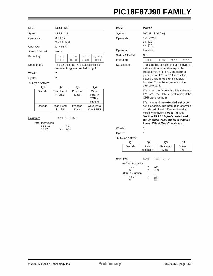
© 2009 Microchip Technology Inc. Preliminary DS39933C-page 357
PIC18F87J90 FAMILY
LFSR Load FSR
Syntax: LFSR f, k
Operands: 0 ≤ f ≤ 20 ≤ k ≤ 4095
Operation: k → FSRf
Status Affected: None
Encoding: 11101111
11100000
00ffk7kkk
k11kkkkkkk
Description: The 12-bit literal ‘k’ is loaded into the file select register pointed to by ‘f’.
Words: 2
Cycles: 2
Q Cycle Activity:Q1 Q2 Q3 Q4
Decode Read literal ‘k’ MSB
Process Data
Writeliteral ‘k’ MSB to FSRfH
Decode Read literal ‘k’ LSB
Process Data
Write literal ‘k’ to FSRfL
Example: LFSR 2, 3ABh
After InstructionFSR2H = 03hFSR2L = ABh
MOVF Move f
Syntax: MOVF f ,d ,a
Operands: 0 ≤ f ≤ 255d ∈ [0,1]a ∈ [0,1]
Operation: f → dest
Status Affected: N, Z
Encoding: 0101 00da ffff ffff
Description: The contents of register ‘f’ are moved to a destination dependent upon the status of ‘d’. If ‘d’ is ‘0’, the result is placed in W. If ‘d’ is ‘1’, the result is placed back in register ‘f’ (default). Location ‘f’ can be anywhere in the 256-byte bank.
If ‘a’ is ‘0’, the Access Bank is selected. If ‘a’ is ‘1’, the BSR is used to select the GPR bank (default).
If ‘a’ is ‘0’ and the extended instruction set is enabled, this instruction operates in Indexed Literal Offset Addressing mode whenever f ≤ 95 (5Fh). See Section 25.2.3 “Byte-Oriented and Bit-Oriented Instructions in Indexed Literal Offset Mode” for details.
Words: 1
Cycles: 1
Q Cycle Activity:Q1 Q2 Q3 Q4
Decode Readregister ‘f’
Process Data
Write W
Example: MOVF REG, 0, 0
Before InstructionREG = 22hW = FFh
After InstructionREG = 22hW = 22h
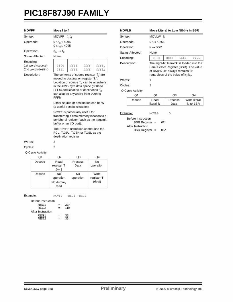
PIC18F87J90 FAMILY
DS39933C-page 358 Preliminary © 2009 Microchip Technology Inc.
MOVFF Move f to f
Syntax: MOVFF fs,fdOperands: 0 ≤ fs ≤ 4095
0 ≤ fd ≤ 4095
Operation: (fs) → fdStatus Affected: None
Encoding:1st word (source)2nd word (destin.)
11001111
ffffffff
ffffffff
ffffsffffd
Description: The contents of source register ‘fs’ are moved to destination register ‘fd’. Location of source ‘fs’ can be anywhere in the 4096-byte data space (000h to FFFh) and location of destination ‘fd’ can also be anywhere from 000h to FFFh.
Either source or destination can be W (a useful special situation).
MOVFF is particularly useful for transferring a data memory location to a peripheral register (such as the transmit buffer or an I/O port).
The MOVFF instruction cannot use the PCL, TOSU, TOSH or TOSL as the destination register
Words: 2
Cycles: 2
Q Cycle Activity:Q1 Q2 Q3 Q4
Decode Readregister ‘f’
(src)
Process Data
No operation
Decode No operation
No dummy read
No operation
Write register ‘f’
(dest)
Example: MOVFF REG1, REG2
Before InstructionREG1 = 33hREG2 = 11h
After InstructionREG1 = 33hREG2 = 33h
MOVLB Move Literal to Low Nibble in BSR
Syntax: MOVLW k
Operands: 0 ≤ k ≤ 255
Operation: k → BSR
Status Affected: None
Encoding: 0000 0001 kkkk kkkk
Description: The eight-bit literal ‘k’ is loaded into the Bank Select Register (BSR). The value of BSR<7:4> always remains ‘0’ regardless of the value of k7:k4.
Words: 1
Cycles: 1
Q Cycle Activity:Q1 Q2 Q3 Q4
Decode Readliteral ‘k’
Process Data
Write literal ‘k’ to BSR
Example: MOVLB 5
Before InstructionBSR Register = 02h
After InstructionBSR Register = 05h
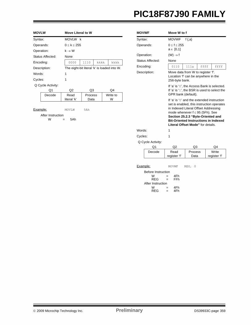
© 2009 Microchip Technology Inc. Preliminary DS39933C-page 359
PIC18F87J90 FAMILY
MOVLW Move Literal to W
Syntax: MOVLW k
Operands: 0 ≤ k ≤ 255
Operation: k → W
Status Affected: None
Encoding: 0000 1110 kkkk kkkk
Description: The eight-bit literal ‘k’ is loaded into W.
Words: 1
Cycles: 1
Q Cycle Activity:Q1 Q2 Q3 Q4
Decode Readliteral ‘k’
Process Data
Write to W
Example: MOVLW 5Ah
After InstructionW = 5Ah
MOVWF Move W to f
Syntax: MOVWF f ,a
Operands: 0 ≤ f ≤ 255a ∈ [0,1]
Operation: (W) → f
Status Affected: None
Encoding: 0110 111a ffff ffff
Description: Move data from W to register ‘f’. Location ‘f’ can be anywhere in the 256-byte bank.
If ‘a’ is ‘0’, the Access Bank is selected. If ‘a’ is ‘1’, the BSR is used to select the GPR bank (default).
If ‘a’ is ‘0’ and the extended instruction set is enabled, this instruction operates in Indexed Literal Offset Addressing mode whenever f ≤ 95 (5Fh). See Section 25.2.3 “Byte-Oriented and Bit-Oriented Instructions in Indexed Literal Offset Mode” for details.
Words: 1
Cycles: 1
Q Cycle Activity:Q1 Q2 Q3 Q4
Decode Readregister ‘f’
Process Data
Writeregister ‘f’
Example: MOVWF REG, 0
Before InstructionW = 4FhREG = FFh
After InstructionW = 4FhREG = 4Fh
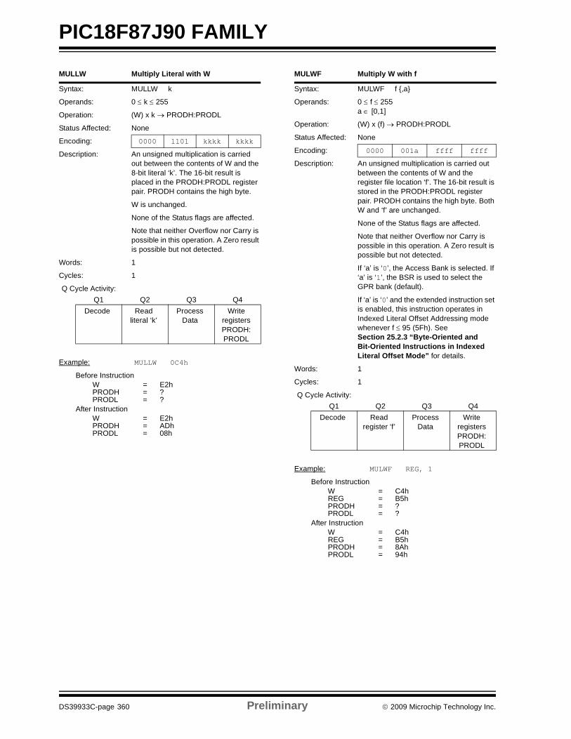
PIC18F87J90 FAMILY
DS39933C-page 360 Preliminary © 2009 Microchip Technology Inc.
MULLW Multiply Literal with W
Syntax: MULLW k
Operands: 0 ≤ k ≤ 255
Operation: (W) x k → PRODH:PRODL
Status Affected: None
Encoding: 0000 1101 kkkk kkkk
Description: An unsigned multiplication is carried out between the contents of W and the 8-bit literal ‘k’. The 16-bit result is placed in the PRODH:PRODL register pair. PRODH contains the high byte.
W is unchanged.
None of the Status flags are affected.
Note that neither Overflow nor Carry is possible in this operation. A Zero result is possible but not detected.
Words: 1
Cycles: 1
Q Cycle Activity:Q1 Q2 Q3 Q4
Decode Read literal ‘k’
Process Data
Write registers PRODH:PRODL
Example: MULLW 0C4h
Before InstructionW = E2hPRODH = ?PRODL = ?
After InstructionW = E2hPRODH = ADhPRODL = 08h
MULWF Multiply W with f
Syntax: MULWF f ,a
Operands: 0 ≤ f ≤ 255a ∈ [0,1]
Operation: (W) x (f) → PRODH:PRODL
Status Affected: None
Encoding: 0000 001a ffff ffff
Description: An unsigned multiplication is carried out between the contents of W and the register file location ‘f’. The 16-bit result is stored in the PRODH:PRODL register pair. PRODH contains the high byte. Both W and ‘f’ are unchanged.
None of the Status flags are affected.
Note that neither Overflow nor Carry is possible in this operation. A Zero result is possible but not detected.
If ‘a’ is ‘0’, the Access Bank is selected. If ‘a’ is ‘1’, the BSR is used to select the GPR bank (default).
If ‘a’ is ‘0’ and the extended instruction set is enabled, this instruction operates in Indexed Literal Offset Addressing mode whenever f ≤ 95 (5Fh). See Section 25.2.3 “Byte-Oriented and Bit-Oriented Instructions in Indexed Literal Offset Mode” for details.
Words: 1
Cycles: 1
Q Cycle Activity:Q1 Q2 Q3 Q4
Decode Readregister ‘f’
Process Data
Writeregisters PRODH:PRODL
Example: MULWF REG, 1
Before InstructionW = C4hREG = B5hPRODH = ?PRODL = ?
After InstructionW = C4hREG = B5hPRODH = 8AhPRODL = 94h
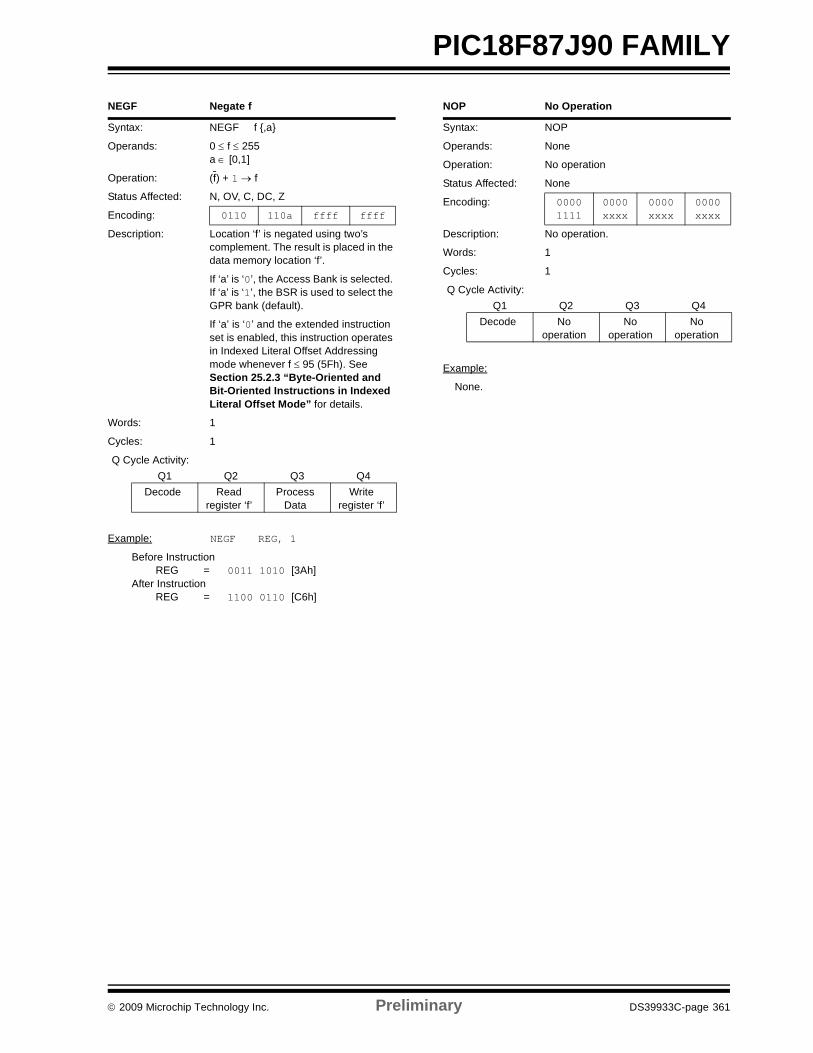
© 2009 Microchip Technology Inc. Preliminary DS39933C-page 361
PIC18F87J90 FAMILY
NEGF Negate f
Syntax: NEGF f ,a
Operands: 0 ≤ f ≤ 255a ∈ [0,1]
Operation: (f) + 1 → f
Status Affected: N, OV, C, DC, Z
Encoding: 0110 110a ffff ffff
Description: Location ‘f’ is negated using two’s complement. The result is placed in the data memory location ‘f’.
If ‘a’ is ‘0’, the Access Bank is selected. If ‘a’ is ‘1’, the BSR is used to select the GPR bank (default).
If ‘a’ is ‘0’ and the extended instruction set is enabled, this instruction operates in Indexed Literal Offset Addressing mode whenever f ≤ 95 (5Fh). See Section 25.2.3 “Byte-Oriented and Bit-Oriented Instructions in Indexed Literal Offset Mode” for details.
Words: 1
Cycles: 1
Q Cycle Activity:Q1 Q2 Q3 Q4
Decode Readregister ‘f’
Process Data
Write register ‘f’
Example: NEGF REG, 1
Before InstructionREG = 0011 1010 [3Ah]
After InstructionREG = 1100 0110 [C6h]
NOP No Operation
Syntax: NOP
Operands: None
Operation: No operation
Status Affected: None
Encoding: 00001111
0000xxxx
0000xxxx
0000xxxx
Description: No operation.
Words: 1
Cycles: 1
Q Cycle Activity:Q1 Q2 Q3 Q4
Decode No operation
No operation
No operation
Example:
None.
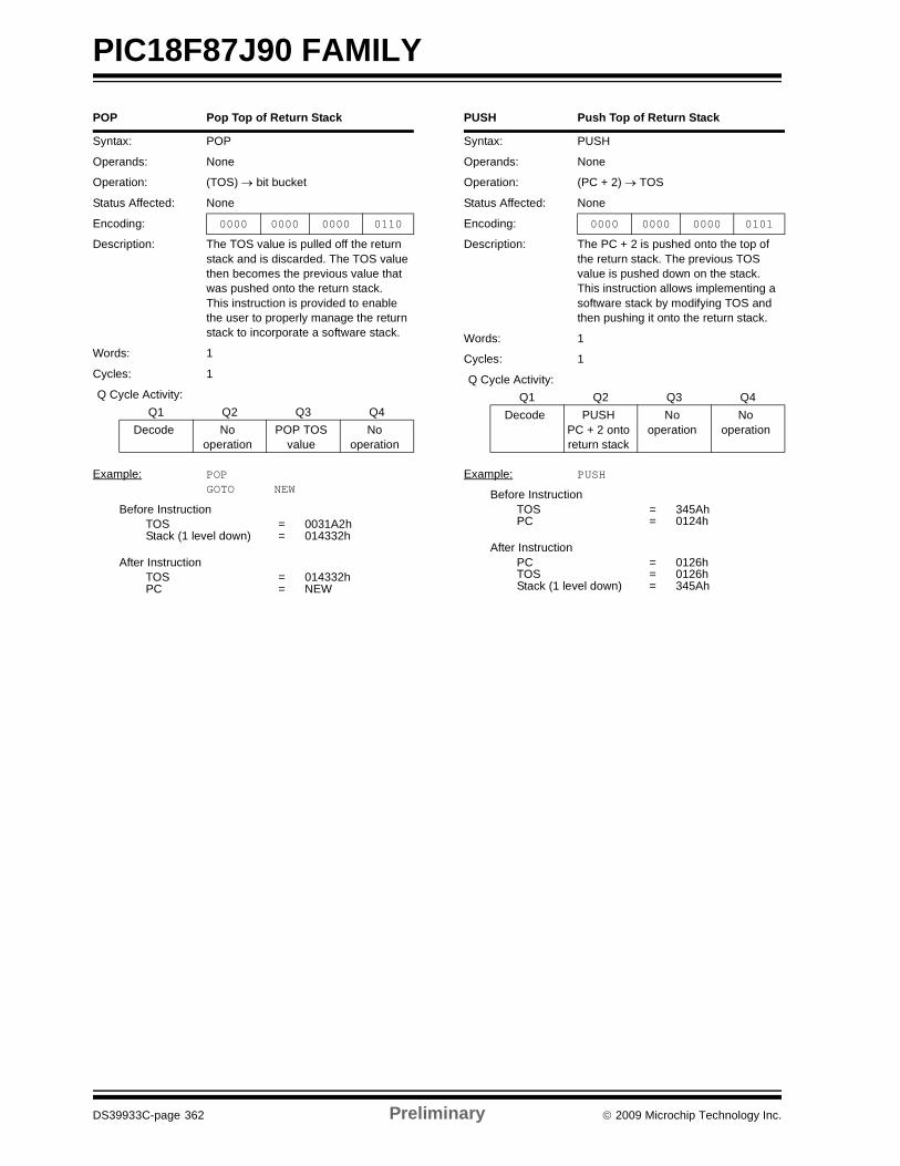
PIC18F87J90 FAMILY
DS39933C-page 362 Preliminary © 2009 Microchip Technology Inc.
POP Pop Top of Return Stack
Syntax: POP
Operands: None
Operation: (TOS) → bit bucket
Status Affected: None
Encoding: 0000 0000 0000 0110
Description: The TOS value is pulled off the return stack and is discarded. The TOS value then becomes the previous value that was pushed onto the return stack.This instruction is provided to enable the user to properly manage the return stack to incorporate a software stack.
Words: 1
Cycles: 1
Q Cycle Activity:Q1 Q2 Q3 Q4
Decode Nooperation
POP TOS value
Nooperation
Example: POPGOTO NEW
Before InstructionTOS = 0031A2hStack (1 level down) = 014332h
After InstructionTOS = 014332hPC = NEW
PUSH Push Top of Return Stack
Syntax: PUSH
Operands: None
Operation: (PC + 2) → TOS
Status Affected: None
Encoding: 0000 0000 0000 0101
Description: The PC + 2 is pushed onto the top of the return stack. The previous TOS value is pushed down on the stack.This instruction allows implementing a software stack by modifying TOS and then pushing it onto the return stack.
Words: 1
Cycles: 1
Q Cycle Activity:Q1 Q2 Q3 Q4
Decode PUSH PC + 2 onto return stack
No operation
No operation
Example: PUSH
Before InstructionTOS = 345AhPC = 0124h
After InstructionPC = 0126hTOS = 0126hStack (1 level down) = 345Ah
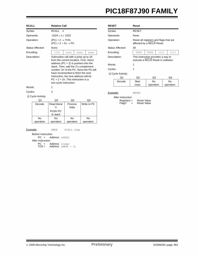
© 2009 Microchip Technology Inc. Preliminary DS39933C-page 363
PIC18F87J90 FAMILY
RCALL Relative Call
Syntax: RCALL n
Operands: -1024 ≤ n ≤ 1023
Operation: (PC) + 2 → TOS,(PC) + 2 + 2n → PC
Status Affected: None
Encoding: 1101 1nnn nnnn nnnn
Description: Subroutine call with a jump up to 1K from the current location. First, return address (PC + 2) is pushed onto the stack. Then, add the 2’s complement number ‘2n’ to the PC. Since the PC will have incremented to fetch the next instruction, the new address will be PC + 2 + 2n. This instruction is a two-cycle instruction.
Words: 1
Cycles: 2
Q Cycle Activity:Q1 Q2 Q3 Q4
Decode Read literal ‘n’
PUSH PC to stack
Process Data
Write to PC
No operation
No operation
No operation
No operation
Example: HERE RCALL Jump
Before InstructionPC = Address (HERE)
After InstructionPC = Address (Jump)TOS = Address (HERE + 2)
RESET Reset
Syntax: RESET
Operands: None
Operation: Reset all registers and flags that are affected by a MCLR Reset.
Status Affected: All
Encoding: 0000 0000 1111 1111
Description: This instruction provides a way to execute a MCLR Reset in software.
Words: 1
Cycles: 1
Q Cycle Activity:Q1 Q2 Q3 Q4
Decode Start reset
No operation
No operation
Example: RESET
After InstructionRegisters = Reset ValueFlags* = Reset Value
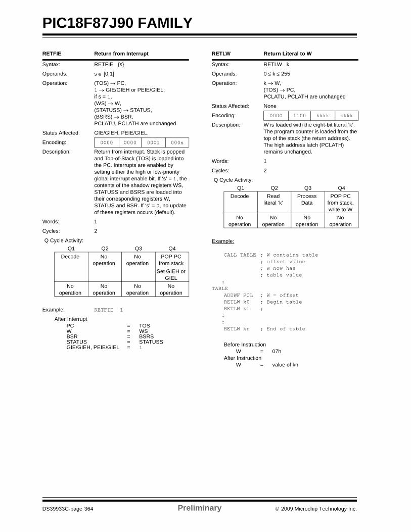
PIC18F87J90 FAMILY
DS39933C-page 364 Preliminary © 2009 Microchip Technology Inc.
RETFIE Return from Interrupt
Syntax: RETFIE s
Operands: s ∈ [0,1]
Operation: (TOS) → PC,1 → GIE/GIEH or PEIE/GIEL;if s = 1,(WS) → W,(STATUSS) → STATUS,(BSRS) → BSR,PCLATU, PCLATH are unchanged
Status Affected: GIE/GIEH, PEIE/GIEL.
Encoding: 0000 0000 0001 000s
Description: Return from interrupt. Stack is popped and Top-of-Stack (TOS) is loaded into the PC. Interrupts are enabled by setting either the high or low-priority global interrupt enable bit. If ‘s’ = 1, the contents of the shadow registers WS, STATUSS and BSRS are loaded into their corresponding registers W, STATUS and BSR. If ‘s’ = 0, no update of these registers occurs (default).
Words: 1
Cycles: 2
Q Cycle Activity:Q1 Q2 Q3 Q4
Decode No operation
No operation
POP PC from stack
Set GIEH or GIEL
No operation
No operation
No operation
No operation
Example: RETFIE 1
After InterruptPC = TOSW = WSBSR = BSRSSTATUS = STATUSSGIE/GIEH, PEIE/GIEL = 1
RETLW Return Literal to W
Syntax: RETLW k
Operands: 0 ≤ k ≤ 255
Operation: k → W,(TOS) → PC,PCLATU, PCLATH are unchanged
Status Affected: None
Encoding: 0000 1100 kkkk kkkk
Description: W is loaded with the eight-bit literal ‘k’. The program counter is loaded from the top of the stack (the return address). The high address latch (PCLATH) remains unchanged.
Words: 1
Cycles: 2
Q Cycle Activity:Q1 Q2 Q3 Q4
Decode Readliteral ‘k’
Process Data
POP PC from stack, write to W
No operation
No operation
No operation
No operation
Example:
CALL TABLE ; W contains table ; offset value ; W now has ; table value :TABLE
ADDWF PCL ; W = offsetRETLW k0 ; Begin tableRETLW k1 ;
: :
RETLW kn ; End of table
Before InstructionW = 07h
After InstructionW = value of kn
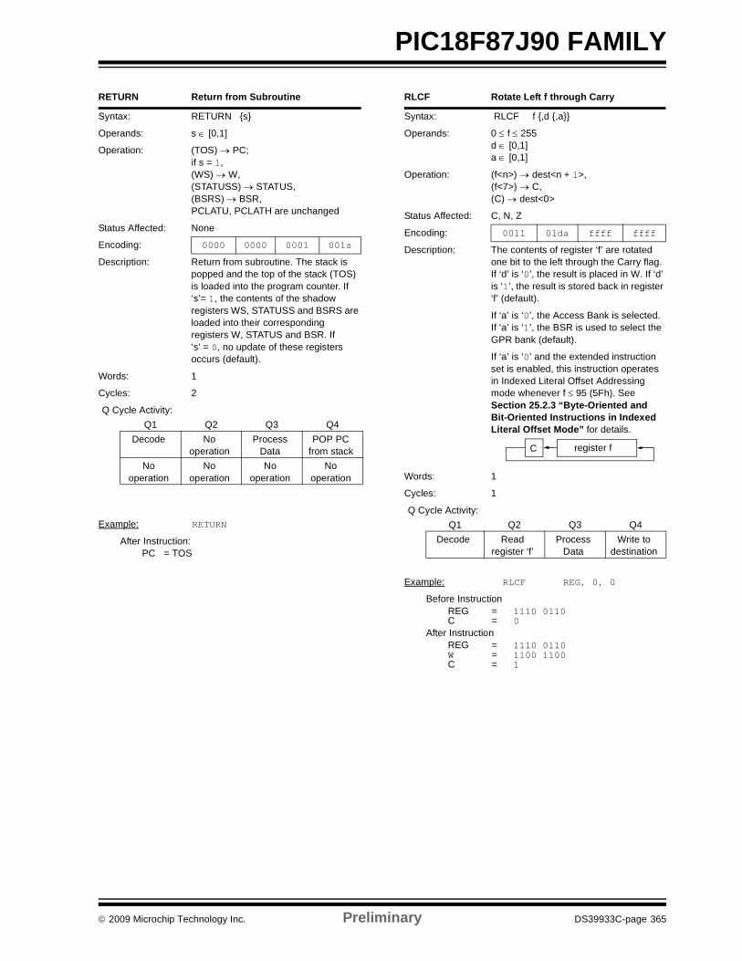
© 2009 Microchip Technology Inc. Preliminary DS39933C-page 365
PIC18F87J90 FAMILY
RETURN Return from Subroutine
Syntax: RETURN s
Operands: s ∈ [0,1]
Operation: (TOS) → PC;if s = 1,(WS) → W,(STATUSS) → STATUS,(BSRS) → BSR,PCLATU, PCLATH are unchanged
Status Affected: None
Encoding: 0000 0000 0001 001s
Description: Return from subroutine. The stack is popped and the top of the stack (TOS) is loaded into the program counter. If ‘s’= 1, the contents of the shadow registers WS, STATUSS and BSRS are loaded into their corresponding registers W, STATUS and BSR. If ‘s’ = 0, no update of these registers occurs (default).
Words: 1
Cycles: 2
Q Cycle Activity:Q1 Q2 Q3 Q4
Decode No operation
Process Data
POP PC from stack
No operation
No operation
No operation
No operation
Example: RETURN
After Instruction:PC = TOS
RLCF Rotate Left f through Carry
Syntax: RLCF f ,d ,a
Operands: 0 ≤ f ≤ 255d ∈ [0,1]a ∈ [0,1]
Operation: (f<n>) → dest<n + 1>,(f<7>) → C,(C) → dest<0>
Status Affected: C, N, Z
Encoding: 0011 01da ffff ffff
Description: The contents of register ‘f’ are rotated one bit to the left through the Carry flag. If ‘d’ is ‘0’, the result is placed in W. If ‘d’ is ‘1’, the result is stored back in register ‘f’ (default).
If ‘a’ is ‘0’, the Access Bank is selected. If ‘a’ is ‘1’, the BSR is used to select the GPR bank (default).
If ‘a’ is ‘0’ and the extended instruction set is enabled, this instruction operates in Indexed Literal Offset Addressing mode whenever f ≤ 95 (5Fh). See Section 25.2.3 “Byte-Oriented and Bit-Oriented Instructions in Indexed Literal Offset Mode” for details.
Words: 1
Cycles: 1
Q Cycle Activity:Q1 Q2 Q3 Q4
Decode Readregister ‘f’
Process Data
Write to destination
Example: RLCF REG, 0, 0
Before InstructionREG = 1110 0110C = 0
After InstructionREG = 1110 0110W = 1100 1100C = 1
C register f
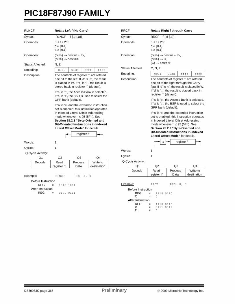
PIC18F87J90 FAMILY
DS39933C-page 366 Preliminary © 2009 Microchip Technology Inc.
RLNCF Rotate Left f (No Carry)
Syntax: RLNCF f ,d ,a
Operands: 0 ≤ f ≤ 255d ∈ [0,1]a ∈ [0,1]
Operation: (f<n>) → dest<n + 1>,(f<7>) → dest<0>
Status Affected: N, Z
Encoding: 0100 01da ffff ffff
Description: The contents of register ‘f’ are rotated one bit to the left. If ‘d’ is ‘0’, the result is placed in W. If ‘d’ is ‘1’, the result is stored back in register ‘f’ (default).
If ‘a’ is ‘0’, the Access Bank is selected. If ‘a’ is ‘1’, the BSR is used to select the GPR bank (default).
If ‘a’ is ‘0’ and the extended instruction set is enabled, this instruction operates in Indexed Literal Offset Addressing mode whenever f ≤ 95 (5Fh). See Section 25.2.3 “Byte-Oriented and Bit-Oriented Instructions in Indexed Literal Offset Mode” for details.
Words: 1
Cycles: 1
Q Cycle Activity:Q1 Q2 Q3 Q4
Decode Readregister ‘f’
Process Data
Write to destination
Example: RLNCF REG, 1, 0
Before InstructionREG = 1010 1011
After InstructionREG = 0101 0111
register f
RRCF Rotate Right f through Carry
Syntax: RRCF f ,d ,a
Operands: 0 ≤ f ≤ 255d ∈ [0,1]a ∈ [0,1]
Operation: (f<n>) → dest<n – 1>,(f<0>) → C,(C) → dest<7>
Status Affected: C, N, Z
Encoding: 0011 00da ffff ffff
Description: The contents of register ‘f’ are rotated one bit to the right through the Carry flag. If ‘d’ is ‘0’, the result is placed in W. If ‘d’ is ‘1’, the result is placed back in register ‘f’ (default).
If ‘a’ is ‘0’, the Access Bank is selected. If ‘a’ is ‘1’, the BSR is used to select the GPR bank (default).
If ‘a’ is ‘0’ and the extended instruction set is enabled, this instruction operates in Indexed Literal Offset Addressing mode whenever f ≤ 95 (5Fh). See Section 25.2.3 “Byte-Oriented and Bit-Oriented Instructions in Indexed Literal Offset Mode” for details.
Words: 1
Cycles: 1
Q Cycle Activity:Q1 Q2 Q3 Q4
Decode Readregister ‘f’
Process Data
Write to destination
Example: RRCF REG, 0, 0
Before InstructionREG = 1110 0110C = 0
After InstructionREG = 1110 0110W = 0111 0011C = 0
C register f
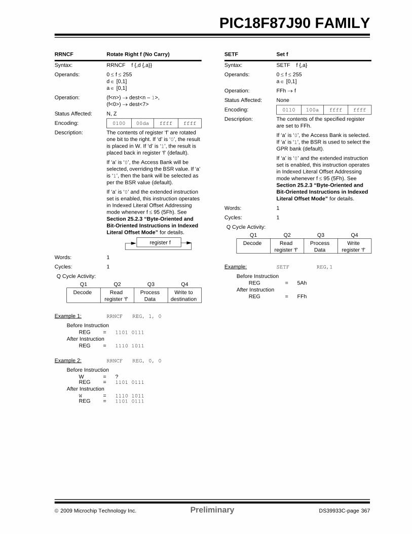
© 2009 Microchip Technology Inc. Preliminary DS39933C-page 367
PIC18F87J90 FAMILY
RRNCF Rotate Right f (No Carry)
Syntax: RRNCF f ,d ,a
Operands: 0 ≤ f ≤ 255d ∈ [0,1]a ∈ [0,1]
Operation: (f<n>) → dest<n – 1>,(f<0>) → dest<7>
Status Affected: N, Z
Encoding: 0100 00da ffff ffff
Description: The contents of register ‘f’ are rotated one bit to the right. If ‘d’ is ‘0’, the result is placed in W. If ‘d’ is ‘1’, the result is placed back in register ‘f’ (default).
If ‘a’ is ‘0’, the Access Bank will be selected, overriding the BSR value. If ‘a’ is ‘1’, then the bank will be selected as per the BSR value (default).
If ‘a’ is ‘0’ and the extended instruction set is enabled, this instruction operates in Indexed Literal Offset Addressing mode whenever f ≤ 95 (5Fh). See Section 25.2.3 “Byte-Oriented and Bit-Oriented Instructions in Indexed Literal Offset Mode” for details.
Words: 1
Cycles: 1
Q Cycle Activity:Q1 Q2 Q3 Q4
Decode Readregister ‘f’
Process Data
Write to destination
Example 1: RRNCF REG, 1, 0
Before InstructionREG = 1101 0111
After InstructionREG = 1110 1011
Example 2: RRNCF REG, 0, 0
Before InstructionW = ?REG = 1101 0111
After InstructionW = 1110 1011REG = 1101 0111
register f
SETF Set f
Syntax: SETF f ,a
Operands: 0 ≤ f ≤ 255a ∈ [0,1]
Operation: FFh → f
Status Affected: None
Encoding: 0110 100a ffff ffff
Description: The contents of the specified register are set to FFh.
If ‘a’ is ‘0’, the Access Bank is selected. If ‘a’ is ‘1’, the BSR is used to select the GPR bank (default).
If ‘a’ is ‘0’ and the extended instruction set is enabled, this instruction operates in Indexed Literal Offset Addressing mode whenever f ≤ 95 (5Fh). See Section 25.2.3 “Byte-Oriented and Bit-Oriented Instructions in Indexed Literal Offset Mode” for details.
Words: 1
Cycles: 1
Q Cycle Activity:Q1 Q2 Q3 Q4
Decode Readregister ‘f’
Process Data
Writeregister ‘f’
Example: SETF REG,1
Before InstructionREG = 5Ah
After InstructionREG = FFh
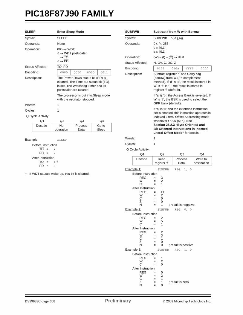
PIC18F87J90 FAMILY
DS39933C-page 368 Preliminary © 2009 Microchip Technology Inc.
SLEEP Enter Sleep Mode
Syntax: SLEEP
Operands: None
Operation: 00h → WDT,0 → WDT postscaler,1 → TO,0 → PD
Status Affected: TO, PD
Encoding: 0000 0000 0000 0011
Description: The Power-Down status bit (PD) is cleared. The Time-out status bit (TO) is set. The Watchdog Timer and its postscaler are cleared.
The processor is put into Sleep mode with the oscillator stopped.
Words: 1
Cycles: 1
Q Cycle Activity:Q1 Q2 Q3 Q4
Decode No operation
Process Data
Go toSleep
Example: SLEEP
Before InstructionTO = ?PD = ?
After InstructionTO = 1 †PD = 0
† If WDT causes wake-up, this bit is cleared.
SUBFWB Subtract f from W with Borrow
Syntax: SUBFWB f ,d ,a
Operands: 0 ≤ f ≤ 255d ∈ [0,1]a ∈ [0,1]
Operation: (W) – (f) – (C) → dest
Status Affected: N, OV, C, DC, Z
Encoding: 0101 01da ffff ffff
Description: Subtract register ‘f’ and Carry flag (borrow) from W (2’s complement method). If ‘d’ is ‘0’, the result is stored in W. If ‘d’ is ‘1’, the result is stored in register ‘f’ (default).
If ‘a’ is ‘0’, the Access Bank is selected. If ‘a’ is ‘1’, the BSR is used to select the GPR bank (default).
If ‘a’ is ‘0’ and the extended instruction set is enabled, this instruction operates in Indexed Literal Offset Addressing mode whenever f ≤ 95 (5Fh). See Section 25.2.3 “Byte-Oriented and Bit-Oriented Instructions in Indexed Literal Offset Mode” for details.
Words: 1
Cycles: 1
Q Cycle Activity:Q1 Q2 Q3 Q4
Decode Readregister ‘f’
Process Data
Write to destination
Example 1: SUBFWB REG, 1, 0Before Instruction
REG = 3W = 2C = 1
After InstructionREG = FFW = 2C = 0Z = 0N = 1 ; result is negative
Example 2: SUBFWB REG, 0, 0
Before InstructionREG = 2W = 5C = 1
After InstructionREG = 2W = 3C = 1Z = 0N = 0 ; result is positive
Example 3: SUBFWB REG, 1, 0
Before InstructionREG = 1W = 2C = 0
After InstructionREG = 0W = 2C = 1Z = 1 ; result is zeroN = 0
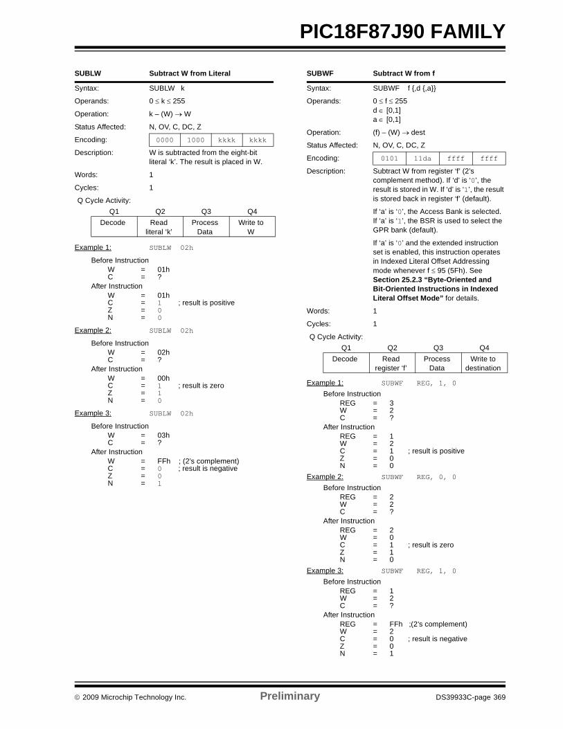
© 2009 Microchip Technology Inc. Preliminary DS39933C-page 369
PIC18F87J90 FAMILY
SUBLW Subtract W from Literal
Syntax: SUBLW k
Operands: 0 ≤ k ≤ 255
Operation: k – (W) → W
Status Affected: N, OV, C, DC, Z
Encoding: 0000 1000 kkkk kkkk
Description: W is subtracted from the eight-bit literal ‘k’. The result is placed in W.
Words: 1
Cycles: 1
Q Cycle Activity:Q1 Q2 Q3 Q4
Decode Readliteral ‘k’
Process Data
Write to W
Example 1: SUBLW 02h
Before InstructionW = 01hC = ?
After InstructionW = 01hC = 1 ; result is positiveZ = 0N = 0
Example 2: SUBLW 02h
Before InstructionW = 02hC = ?
After InstructionW = 00hC = 1 ; result is zeroZ = 1N = 0
Example 3: SUBLW 02h
Before InstructionW = 03hC = ?
After InstructionW = FFh ; (2’s complement)C = 0 ; result is negativeZ = 0N = 1
SUBWF Subtract W from f
Syntax: SUBWF f ,d ,a
Operands: 0 ≤ f ≤ 255d ∈ [0,1]a ∈ [0,1]
Operation: (f) – (W) → dest
Status Affected: N, OV, C, DC, Z
Encoding: 0101 11da ffff ffff
Description: Subtract W from register ‘f’ (2’s complement method). If ‘d’ is ‘0’, the result is stored in W. If ‘d’ is ‘1’, the result is stored back in register ‘f’ (default).
If ‘a’ is ‘0’, the Access Bank is selected. If ‘a’ is ‘1’, the BSR is used to select the GPR bank (default).
If ‘a’ is ‘0’ and the extended instruction set is enabled, this instruction operates in Indexed Literal Offset Addressing mode whenever f ≤ 95 (5Fh). See Section 25.2.3 “Byte-Oriented and Bit-Oriented Instructions in Indexed Literal Offset Mode” for details.
Words: 1
Cycles: 1
Q Cycle Activity:Q1 Q2 Q3 Q4
Decode Readregister ‘f’
Process Data
Write to destination
Example 1: SUBWF REG, 1, 0
Before InstructionREG = 3W = 2C = ?
After InstructionREG = 1W = 2C = 1 ; result is positiveZ = 0N = 0
Example 2: SUBWF REG, 0, 0
Before InstructionREG = 2W = 2C = ?
After InstructionREG = 2W = 0C = 1 ; result is zeroZ = 1N = 0
Example 3: SUBWF REG, 1, 0
Before InstructionREG = 1W = 2C = ?
After InstructionREG = FFh ;(2’s complement)W = 2C = 0 ; result is negativeZ = 0N = 1
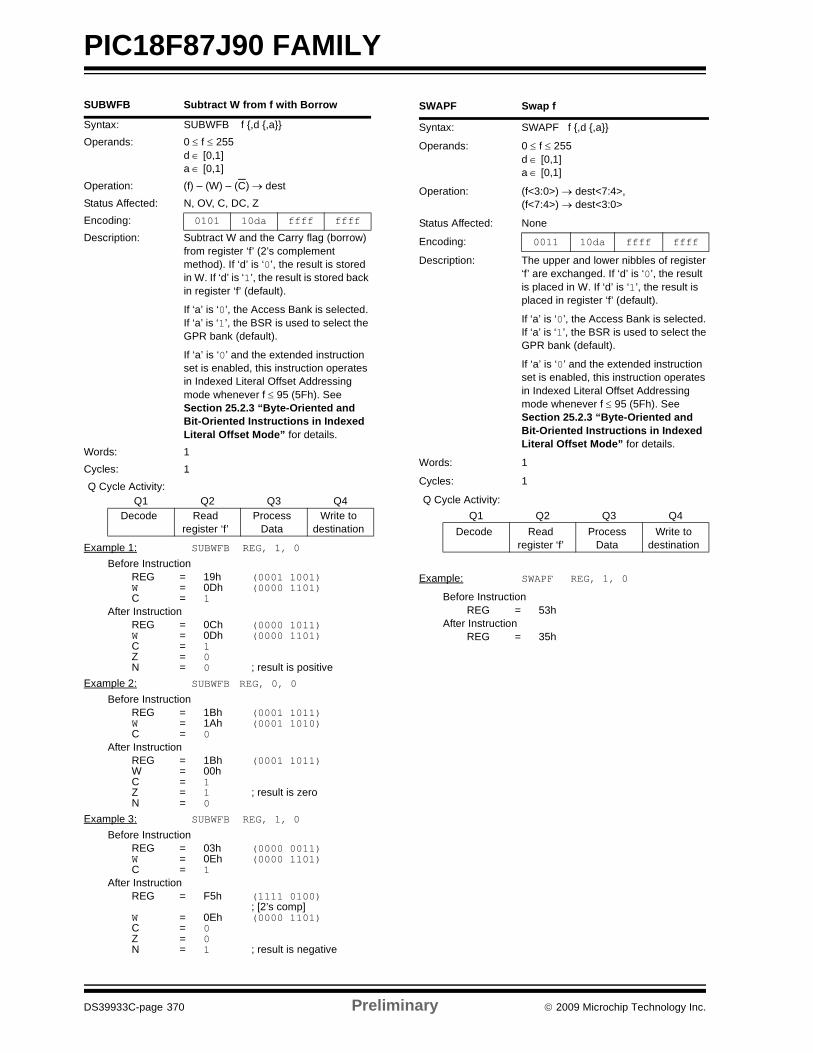
PIC18F87J90 FAMILY
DS39933C-page 370 Preliminary © 2009 Microchip Technology Inc.
SUBWFB Subtract W from f with Borrow
Syntax: SUBWFB f ,d ,aOperands: 0 ≤ f ≤ 255
d ∈ [0,1]a ∈ [0,1]
Operation: (f) – (W) – (C) → destStatus Affected: N, OV, C, DC, ZEncoding: 0101 10da ffff ffff
Description: Subtract W and the Carry flag (borrow) from register ‘f’ (2’s complement method). If ‘d’ is ‘0’, the result is stored in W. If ‘d’ is ‘1’, the result is stored back in register ‘f’ (default).
If ‘a’ is ‘0’, the Access Bank is selected. If ‘a’ is ‘1’, the BSR is used to select the GPR bank (default).
If ‘a’ is ‘0’ and the extended instruction set is enabled, this instruction operates in Indexed Literal Offset Addressing mode whenever f ≤ 95 (5Fh). See Section 25.2.3 “Byte-Oriented and Bit-Oriented Instructions in Indexed Literal Offset Mode” for details.
Words: 1Cycles: 1Q Cycle Activity:
Q1 Q2 Q3 Q4Decode Read
register ‘f’Process
DataWrite to
destination
Example 1: SUBWFB REG, 1, 0
Before InstructionREG = 19h (0001 1001)W = 0Dh (0000 1101)C = 1
After InstructionREG = 0Ch (0000 1011)W = 0Dh (0000 1101)C = 1Z = 0N = 0 ; result is positive
Example 2: SUBWFB REG, 0, 0
Before InstructionREG = 1Bh (0001 1011)W = 1Ah (0001 1010)C = 0
After InstructionREG = 1Bh (0001 1011)W = 00hC = 1Z = 1 ; result is zeroN = 0
Example 3: SUBWFB REG, 1, 0
Before InstructionREG = 03h (0000 0011)W = 0Eh (0000 1101)C = 1
After InstructionREG = F5h (1111 0100)
; [2’s comp]W = 0Eh (0000 1101)C = 0Z = 0N = 1 ; result is negative
SWAPF Swap f
Syntax: SWAPF f ,d ,a
Operands: 0 ≤ f ≤ 255d ∈ [0,1]a ∈ [0,1]
Operation: (f<3:0>) → dest<7:4>,(f<7:4>) → dest<3:0>
Status Affected: None
Encoding: 0011 10da ffff ffff
Description: The upper and lower nibbles of register ‘f’ are exchanged. If ‘d’ is ‘0’, the result is placed in W. If ‘d’ is ‘1’, the result is placed in register ‘f’ (default).
If ‘a’ is ‘0’, the Access Bank is selected. If ‘a’ is ‘1’, the BSR is used to select the GPR bank (default).
If ‘a’ is ‘0’ and the extended instruction set is enabled, this instruction operates in Indexed Literal Offset Addressing mode whenever f ≤ 95 (5Fh). See Section 25.2.3 “Byte-Oriented and Bit-Oriented Instructions in Indexed Literal Offset Mode” for details.
Words: 1
Cycles: 1
Q Cycle Activity:Q1 Q2 Q3 Q4
Decode Readregister ‘f’
Process Data
Write to destination
Example: SWAPF REG, 1, 0
Before InstructionREG = 53h
After InstructionREG = 35h
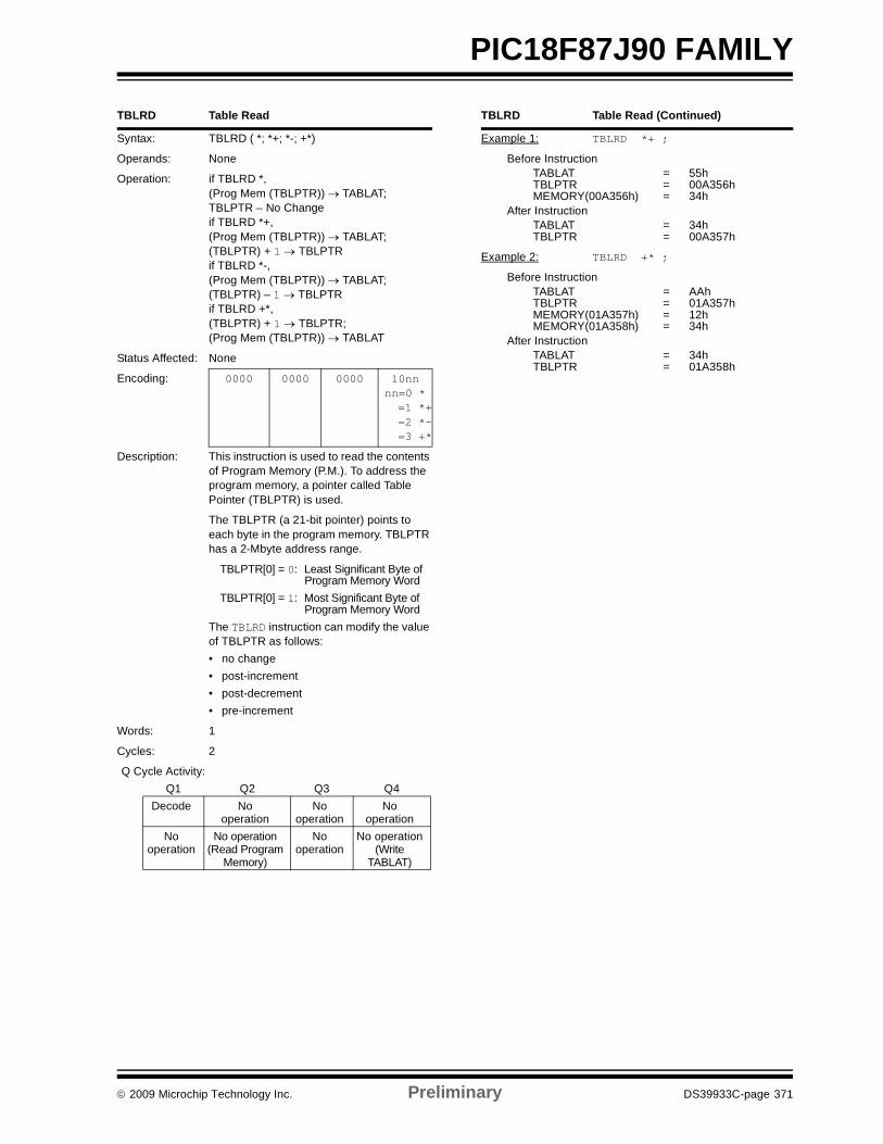
© 2009 Microchip Technology Inc. Preliminary DS39933C-page 371
PIC18F87J90 FAMILY
TBLRD Table Read
Syntax: TBLRD ( *; *+; *-; +*)
Operands: None
Operation: if TBLRD *,(Prog Mem (TBLPTR)) → TABLAT;TBLPTR – No Changeif TBLRD *+,(Prog Mem (TBLPTR)) → TABLAT;(TBLPTR) + 1 → TBLPTRif TBLRD *-,(Prog Mem (TBLPTR)) → TABLAT;(TBLPTR) – 1 → TBLPTRif TBLRD +*,(TBLPTR) + 1 → TBLPTR;(Prog Mem (TBLPTR)) → TABLAT
Status Affected: None
Encoding: 0000 0000 0000 10nn nn=0 * =1 *+ =2 *- =3 +*
Description: This instruction is used to read the contents of Program Memory (P.M.). To address the program memory, a pointer called Table Pointer (TBLPTR) is used.
The TBLPTR (a 21-bit pointer) points to each byte in the program memory. TBLPTR has a 2-Mbyte address range.
TBLPTR[0] = 0: Least Significant Byte of Program Memory Word
TBLPTR[0] = 1: Most Significant Byte of Program Memory Word
The TBLRD instruction can modify the value of TBLPTR as follows:• no change• post-increment• post-decrement• pre-increment
Words: 1
Cycles: 2
Q Cycle Activity:Q1 Q2 Q3 Q4
Decode No operation
No operation
No operation
No operation
No operation(Read Program
Memory)
No operation
No operation(Write
TABLAT)
TBLRD Table Read (Continued)
Example 1: TBLRD *+ ;
Before InstructionTABLAT = 55hTBLPTR = 00A356hMEMORY(00A356h) = 34h
After InstructionTABLAT = 34hTBLPTR = 00A357h
Example 2: TBLRD +* ;
Before InstructionTABLAT = AAhTBLPTR = 01A357hMEMORY(01A357h) = 12hMEMORY(01A358h) = 34h
After InstructionTABLAT = 34hTBLPTR = 01A358h
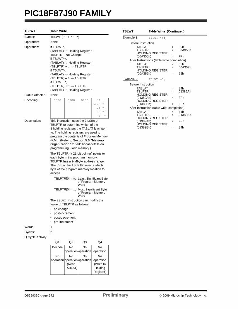
PIC18F87J90 FAMILY
DS39933C-page 372 Preliminary © 2009 Microchip Technology Inc.
TBLWT Table Write
Syntax: TBLWT ( *; *+; *-; +*)Operands: NoneOperation: if TBLWT*,
(TABLAT) → Holding Register;TBLPTR – No Changeif TBLWT*+,(TABLAT) → Holding Register;(TBLPTR) + 1 → TBLPTRif TBLWT*-,(TABLAT) → Holding Register;(TBLPTR) – 1 → TBLPTRif TBLWT+*,(TBLPTR) + 1 → TBLPTR;(TABLAT) → Holding Register
Status Affected: NoneEncoding: 0000 0000 0000 11nn
nn=0 * =1 *+ =2 *- =3 +*
Description: This instruction uses the 3 LSBs of TBLPTR to determine which of the 8 holding registers the TABLAT is written to. The holding registers are used to program the contents of Program Memory (P.M.). (Refer to Section 5.0 “Memory Organization” for additional details on programming Flash memory.)
The TBLPTR (a 21-bit pointer) points to each byte in the program memory. TBLPTR has a 2-Mbyte address range. The LSb of the TBLPTR selects which byte of the program memory location to access.
TBLPTR[0] = 0: Least Significant Byte of Program Memory Word
TBLPTR[0] = 1: Most Significant Byte of Program Memory Word
The TBLWT instruction can modify the value of TBLPTR as follows:• no change• post-increment• post-decrement• pre-increment
Words: 1Cycles: 2 Q Cycle Activity:
Q1 Q2 Q3 Q4Decode No
operationNo
operationNo
operationNo
operationNo
operation(Read
TABLAT)
No operation
No operation(Write to Holding
Register)
TBLWT Table Write (Continued)
Example 1: TBLWT *+;
Before InstructionTABLAT = 55hTBLPTR = 00A356hHOLDING REGISTER (00A356h) = FFh
After Instructions (table write completion)TABLAT = 55hTBLPTR = 00A357hHOLDING REGISTER (00A356h) = 55h
Example 2: TBLWT +*;
Before InstructionTABLAT = 34hTBLPTR = 01389AhHOLDING REGISTER (01389Ah) = FFhHOLDING REGISTER (01389Bh) = FFh
After Instruction (table write completion)TABLAT = 34hTBLPTR = 01389BhHOLDING REGISTER (01389Ah) = FFhHOLDING REGISTER (01389Bh) = 34h
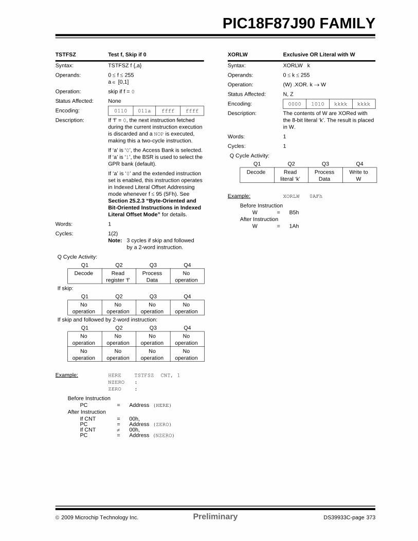
© 2009 Microchip Technology Inc. Preliminary DS39933C-page 373
PIC18F87J90 FAMILY
TSTFSZ Test f, Skip if 0
Syntax: TSTFSZ f ,a
Operands: 0 ≤ f ≤ 255a ∈ [0,1]
Operation: skip if f = 0
Status Affected: None
Encoding: 0110 011a ffff ffff
Description: If ‘f’ = 0, the next instruction fetched during the current instruction execution is discarded and a NOP is executed, making this a two-cycle instruction.
If ‘a’ is ‘0’, the Access Bank is selected. If ‘a’ is ‘1’, the BSR is used to select the GPR bank (default).
If ‘a’ is ‘0’ and the extended instruction set is enabled, this instruction operates in Indexed Literal Offset Addressing mode whenever f ≤ 95 (5Fh). See Section 25.2.3 “Byte-Oriented and Bit-Oriented Instructions in Indexed Literal Offset Mode” for details.
Words: 1
Cycles: 1(2)Note: 3 cycles if skip and followed
by a 2-word instruction.
Q Cycle Activity:Q1 Q2 Q3 Q4
Decode Readregister ‘f’
Process Data
No operation
If skip:Q1 Q2 Q3 Q4No
operationNo
operationNo
operationNo
operationIf skip and followed by 2-word instruction:
Q1 Q2 Q3 Q4No
operationNo
operationNo
operationNo
operationNo
operationNo
operationNo
operationNo
operation
Example: HERE TSTFSZ CNT, 1NZERO :ZERO :
Before InstructionPC = Address (HERE)
After InstructionIf CNT = 00h,PC = Address (ZERO)If CNT ≠ 00h,PC = Address (NZERO)
XORLW Exclusive OR Literal with W
Syntax: XORLW k
Operands: 0 ≤ k ≤ 255
Operation: (W) .XOR. k → W
Status Affected: N, Z
Encoding: 0000 1010 kkkk kkkk
Description: The contents of W are XORed with the 8-bit literal ‘k’. The result is placed in W.
Words: 1
Cycles: 1
Q Cycle Activity:Q1 Q2 Q3 Q4
Decode Readliteral ‘k’
Process Data
Write to W
Example: XORLW 0AFh
Before InstructionW = B5h
After InstructionW = 1Ah
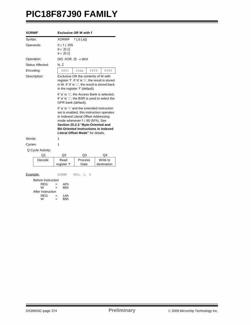
PIC18F87J90 FAMILY
DS39933C-page 374 Preliminary © 2009 Microchip Technology Inc.
XORWF Exclusive OR W with f
Syntax: XORWF f ,d ,a
Operands: 0 ≤ f ≤ 255d ∈ [0,1]a ∈ [0,1]
Operation: (W) .XOR. (f) → dest
Status Affected: N, Z
Encoding: 0001 10da ffff ffff
Description: Exclusive OR the contents of W with register ‘f’. If ‘d’ is ‘0’, the result is stored in W. If ‘d’ is ‘1’, the result is stored back in the register ‘f’ (default).
If ‘a’ is ‘0’, the Access Bank is selected. If ‘a’ is ‘1’, the BSR is used to select the GPR bank (default).
If ‘a’ is ‘0’ and the extended instruction set is enabled, this instruction operates in Indexed Literal Offset Addressing mode whenever f ≤ 95 (5Fh). See Section 25.2.3 “Byte-Oriented and Bit-Oriented Instructions in Indexed Literal Offset Mode” for details.
Words: 1
Cycles: 1
Q Cycle Activity:Q1 Q2 Q3 Q4
Decode Readregister ‘f’
Process Data
Write to destination
Example: XORWF REG, 1, 0
Before InstructionREG = AFhW = B5h
After InstructionREG = 1AhW = B5h
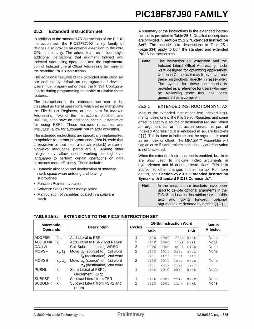
© 2009 Microchip Technology Inc. Preliminary DS39933C-page 375
PIC18F87J90 FAMILY25.2 Extended Instruction SetIn addition to the standard 75 instructions of the PIC18instruction set, the PIC18F87J90 family family ofdevices also provide an optional extension to the coreCPU functionality. The added features include eightadditional instructions that augment Indirect andIndexed Addressing operations and the implementa-tion of Indexed Literal Offset Addressing for many ofthe standard PIC18 instructions.
The additional features of the extended instruction setare enabled by default on unprogrammed devices.Users must properly set or clear the XINST Configura-tion bit during programming to enable or disable thesefeatures.
The instructions in the extended set can all beclassified as literal operations, which either manipulatethe File Select Registers, or use them for IndexedAddressing. Two of the instructions, ADDFSR andSUBFSR, each have an additional special instantiationfor using FSR2. These versions (ADDULNK andSUBULNK) allow for automatic return after execution.
The extended instructions are specifically implementedto optimize re-entrant program code (that is, code thatis recursive or that uses a software stack) written inhigh-level languages, particularly C. Among otherthings, they allow users working in high-levellanguages to perform certain operations on datastructures more efficiently. These include:
• Dynamic allocation and deallocation of software stack space when entering and leaving subroutines
• Function Pointer invocation• Software Stack Pointer manipulation• Manipulation of variables located in a software
stack
A summary of the instructions in the extended instruc-tion set is provided in Table 25-3. Detailed descriptionsare provided in Section 25.2.2 “Extended InstructionSet”. The opcode field descriptions in Table 25-1(page 334) apply to both the standard and extendedPIC18 instruction sets.
25.2.1 EXTENDED INSTRUCTION SYNTAXMost of the extended instructions use indexed argu-ments, using one of the File Select Registers and someoffset to specify a source or destination register. Whenan argument for an instruction serves as part ofIndexed Addressing, it is enclosed in square brackets(“[ ]”). This is done to indicate that the argument is usedas an index or offset. The MPASM™ Assembler willflag an error if it determines that an index or offset valueis not bracketed.
When the extended instruction set is enabled, bracketsare also used to indicate index arguments inbyte-oriented and bit-oriented instructions. This is inaddition to other changes in their syntax. For moredetails, see Section 25.2.3.1 “Extended InstructionSyntax with Standard PIC18 Commands”.
TABLE 25-3: EXTENSIONS TO THE PIC18 INSTRUCTION SET
Note: The instruction set extension and theIndexed Literal Offset Addressing modewere designed for optimizing applicationswritten in C; the user may likely never usethese instructions directly in assembler.The syntax for these commands isprovided as a reference for users who maybe reviewing code that has beengenerated by a compiler.
Note: In the past, square brackets have beenused to denote optional arguments in thePIC18 and earlier instruction sets. In thistext and going forward, optionalarguments are denoted by braces (“ ”).
Mnemonic,Operands Description Cycles
16-Bit Instruction Word StatusAffectedMSb LSb
ADDFSRADDULNKCALLWMOVSF
MOVSS
PUSHL
SUBFSRSUBULNK
f, kk
zs, fd
zs, zd
k
f, kk
Add Literal to FSRAdd Literal to FSR2 and ReturnCall Subroutine using WREGMove zs (source) to 1st word
fd (destination) 2nd wordMove zs (source) to 1st word
zd (destination) 2nd wordStore Literal at FSR2, Decrement FSR2Subtract Literal from FSRSubtract Literal from FSR2 and return
1222
2
1
12
11101110000011101111111011111110
11101110
1000100000001011ffff1011xxxx1010
10011001
ffkk 11kk 00010zzzffff1zzzxzzzkkkk
ffkk11kk
kkkkkkkk0100zzzzffffzzzzzzzzkkkk
kkkkkkkk
NoneNoneNoneNone
None
None
NoneNone
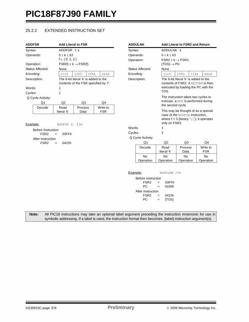
PIC18F87J90 FAMILY
DS39933C-page 376 Preliminary © 2009 Microchip Technology Inc.
25.2.2 EXTENDED INSTRUCTION SET
ADDFSR Add Literal to FSR
Syntax: ADDFSR f, kOperands: 0 ≤ k ≤ 63
f ∈ [ 0, 1, 2 ]Operation: FSR(f) + k → FSR(f)Status Affected: NoneEncoding: 1110 1000 ffkk kkkk
Description: The 6-bit literal ‘k’ is added to the contents of the FSR specified by ‘f’.
Words: 1Cycles: 1Q Cycle Activity:
Q1 Q2 Q3 Q4Decode Read
literal ‘k’Process
DataWrite to
FSR
Example: ADDFSR 2, 23h
Before InstructionFSR2 = 03FFh
After InstructionFSR2 = 0422h
ADDULNK Add Literal to FSR2 and Return
Syntax: ADDULNK kOperands: 0 ≤ k ≤ 63Operation: FSR2 + k → FSR2,
(TOS) → PCStatus Affected: NoneEncoding: 1110 1000 11kk kkkk
Description: The 6-bit literal ‘k’ is added to the contents of FSR2. A RETURN is then executed by loading the PC with the TOS.
The instruction takes two cycles to execute; a NOP is performed during the second cycle.
This may be thought of as a special case of the ADDFSR instruction, where f = 3 (binary ‘11’); it operates only on FSR2.
Words: 1Cycles: 2Q Cycle Activity:
Q1 Q2 Q3 Q4Decode Read
literal ‘k’Process
DataWrite to
FSRNo
OperationNo
OperationNo
OperationNo
Operation
Example: ADDULNK 23h
Before InstructionFSR2 = 03FFhPC = 0100h
After InstructionFSR2 = 0422hPC = (TOS)
Note: All PIC18 instructions may take an optional label argument preceding the instruction mnemonic for use insymbolic addressing. If a label is used, the instruction format then becomes: label instruction argument(s).
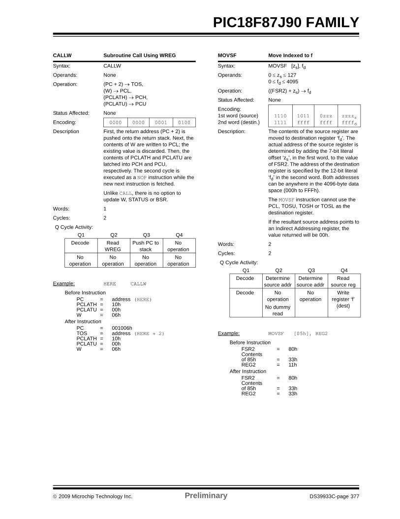
© 2009 Microchip Technology Inc. Preliminary DS39933C-page 377
PIC18F87J90 FAMILY
CALLW Subroutine Call Using WREG
Syntax: CALLW
Operands: None
Operation: (PC + 2) → TOS,(W) → PCL,(PCLATH) → PCH,(PCLATU) → PCU
Status Affected: None
Encoding: 0000 0000 0001 0100
Description First, the return address (PC + 2) is pushed onto the return stack. Next, the contents of W are written to PCL; the existing value is discarded. Then, the contents of PCLATH and PCLATU are latched into PCH and PCU, respectively. The second cycle is executed as a NOP instruction while the new next instruction is fetched.
Unlike CALL, there is no option to update W, STATUS or BSR.
Words: 1
Cycles: 2
Q Cycle Activity:Q1 Q2 Q3 Q4
Decode Read WREG
Push PC to stack
No operation
No operation
No operation
No operation
No operation
Example: HERE CALLW
Before InstructionPC = address (HERE)PCLATH = 10hPCLATU = 00hW = 06h
After InstructionPC = 001006hTOS = address (HERE + 2)PCLATH = 10hPCLATU = 00hW = 06h
MOVSF Move Indexed to f
Syntax: MOVSF [zs], fdOperands: 0 ≤ zs ≤ 127
0 ≤ fd ≤ 4095
Operation: ((FSR2) + zs) → fdStatus Affected: None
Encoding:1st word (source)2nd word (destin.)
11101111
1011ffff
0zzzffff
zzzzsffffd
Description: The contents of the source register are moved to destination register ‘fd’. The actual address of the source register is determined by adding the 7-bit literal offset ‘zs’, in the first word, to the value of FSR2. The address of the destination register is specified by the 12-bit literal ‘fd’ in the second word. Both addresses can be anywhere in the 4096-byte data space (000h to FFFh).
The MOVSF instruction cannot use the PCL, TOSU, TOSH or TOSL as the destination register.
If the resultant source address points to an Indirect Addressing register, the value returned will be 00h.
Words: 2
Cycles: 2
Q Cycle Activity:Q1 Q2 Q3 Q4
Decode Determine source addr
Determinesource addr
Read source reg
Decode No operation
No dummy read
No operation
Write register ‘f’
(dest)
Example: MOVSF [05h], REG2
Before InstructionFSR2 = 80hContents of 85h = 33hREG2 = 11h
After InstructionFSR2 = 80hContentsof 85h = 33hREG2 = 33h
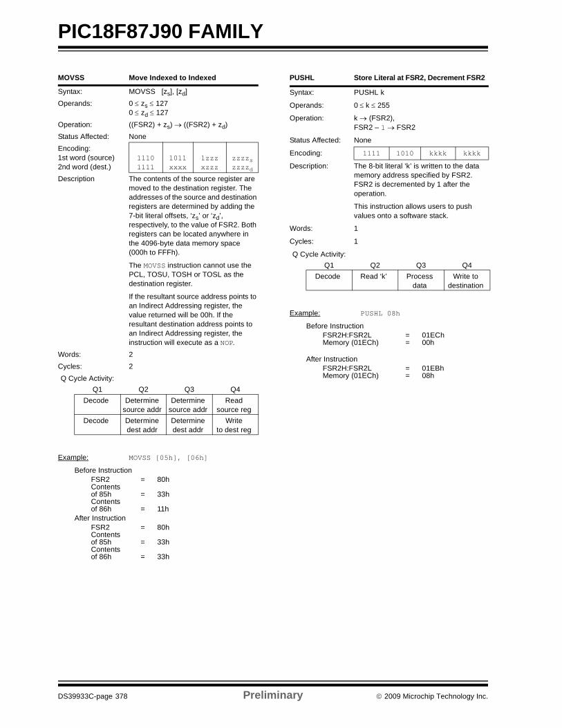
PIC18F87J90 FAMILY
DS39933C-page 378 Preliminary © 2009 Microchip Technology Inc.
MOVSS Move Indexed to Indexed
Syntax: MOVSS [zs], [zd]Operands: 0 ≤ zs ≤ 127
0 ≤ zd ≤ 127Operation: ((FSR2) + zs) → ((FSR2) + zd)Status Affected: NoneEncoding:1st word (source)2nd word (dest.)
11101111
1011xxxx
1zzzxzzz
zzzzszzzzd
Description The contents of the source register are moved to the destination register. The addresses of the source and destination registers are determined by adding the 7-bit literal offsets, ‘zs’ or ‘zd’, respectively, to the value of FSR2. Both registers can be located anywhere in the 4096-byte data memory space (000h to FFFh).
The MOVSS instruction cannot use the PCL, TOSU, TOSH or TOSL as the destination register.
If the resultant source address points to an Indirect Addressing register, the value returned will be 00h. If the resultant destination address points to an Indirect Addressing register, the instruction will execute as a NOP.
Words: 2Cycles: 2Q Cycle Activity:
Q1 Q2 Q3 Q4Decode Determine
source addrDetermine
source addrRead
source regDecode Determine
dest addrDeterminedest addr
Write to dest reg
Example: MOVSS [05h], [06h]
Before InstructionFSR2 = 80hContentsof 85h = 33hContentsof 86h = 11h
After InstructionFSR2 = 80hContentsof 85h = 33hContentsof 86h = 33h
PUSHL Store Literal at FSR2, Decrement FSR2
Syntax: PUSHL k
Operands: 0 ≤ k ≤ 255
Operation: k → (FSR2),FSR2 – 1 → FSR2
Status Affected: None
Encoding: 1111 1010 kkkk kkkk
Description: The 8-bit literal ‘k’ is written to the data memory address specified by FSR2. FSR2 is decremented by 1 after the operation.
This instruction allows users to push values onto a software stack.
Words: 1
Cycles: 1
Q Cycle Activity:Q1 Q2 Q3 Q4
Decode Read ‘k’ Processdata
Write todestination
Example: PUSHL 08h
Before InstructionFSR2H:FSR2L = 01EChMemory (01ECh) = 00h
After InstructionFSR2H:FSR2L = 01EBhMemory (01ECh) = 08h
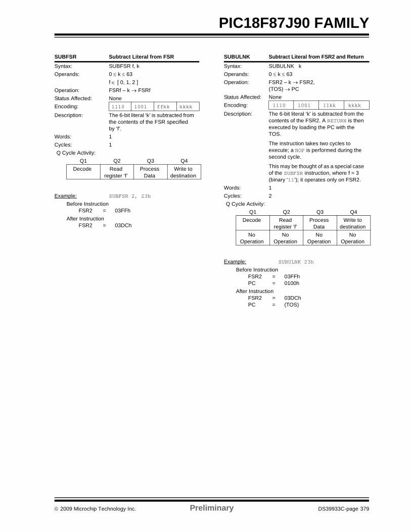
© 2009 Microchip Technology Inc. Preliminary DS39933C-page 379
PIC18F87J90 FAMILY
SUBFSR Subtract Literal from FSR
Syntax: SUBFSR f, kOperands: 0 ≤ k ≤ 63
f ∈ [ 0, 1, 2 ]Operation: FSRf – k → FSRfStatus Affected: NoneEncoding: 1110 1001 ffkk kkkk
Description: The 6-bit literal ‘k’ is subtracted from the contents of the FSR specified by ‘f’.
Words: 1Cycles: 1Q Cycle Activity:
Q1 Q2 Q3 Q4Decode Read
register ‘f’Process
DataWrite to
destination
Example: SUBFSR 2, 23h
Before InstructionFSR2 = 03FFh
After InstructionFSR2 = 03DCh
SUBULNK Subtract Literal from FSR2 and Return
Syntax: SUBULNK kOperands: 0 ≤ k ≤ 63Operation: FSR2 – k → FSR2,
(TOS) → PCStatus Affected: NoneEncoding: 1110 1001 11kk kkkk
Description: The 6-bit literal ‘k’ is subtracted from the contents of the FSR2. A RETURN is then executed by loading the PC with the TOS.
The instruction takes two cycles to execute; a NOP is performed during the second cycle.
This may be thought of as a special case of the SUBFSR instruction, where f = 3 (binary ‘11’); it operates only on FSR2.
Words: 1Cycles: 2Q Cycle Activity:
Q1 Q2 Q3 Q4Decode Read
register ‘f’Process
DataWrite to
destinationNo
OperationNo
OperationNo
OperationNo
Operation
Example: SUBULNK 23h
Before InstructionFSR2 = 03FFhPC = 0100h
After InstructionFSR2 = 03DChPC = (TOS)
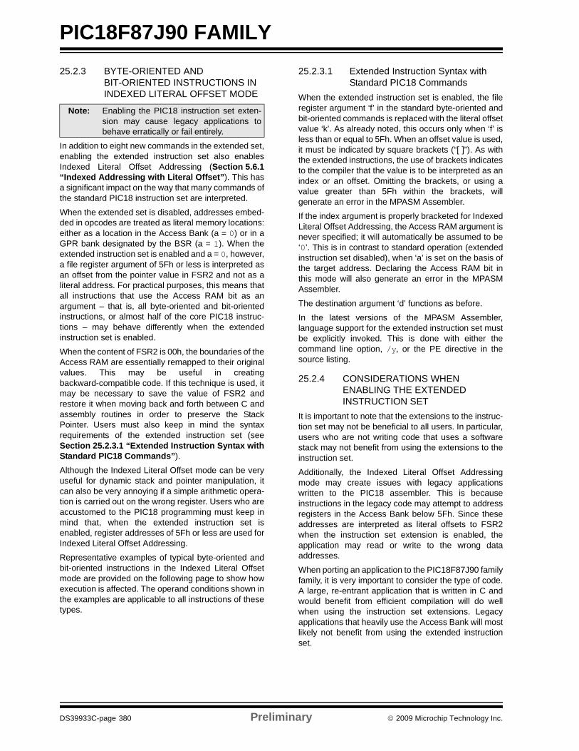
PIC18F87J90 FAMILY
DS39933C-page 380 Preliminary © 2009 Microchip Technology Inc.
25.2.3 BYTE-ORIENTED AND BIT-ORIENTED INSTRUCTIONS IN INDEXED LITERAL OFFSET MODE
In addition to eight new commands in the extended set,enabling the extended instruction set also enablesIndexed Literal Offset Addressing (Section 5.6.1“Indexed Addressing with Literal Offset”). This hasa significant impact on the way that many commands ofthe standard PIC18 instruction set are interpreted.
When the extended set is disabled, addresses embed-ded in opcodes are treated as literal memory locations:either as a location in the Access Bank (a = 0) or in aGPR bank designated by the BSR (a = 1). When theextended instruction set is enabled and a = 0, however,a file register argument of 5Fh or less is interpreted asan offset from the pointer value in FSR2 and not as aliteral address. For practical purposes, this means thatall instructions that use the Access RAM bit as anargument – that is, all byte-oriented and bit-orientedinstructions, or almost half of the core PIC18 instruc-tions – may behave differently when the extendedinstruction set is enabled.
When the content of FSR2 is 00h, the boundaries of theAccess RAM are essentially remapped to their originalvalues. This may be useful in creatingbackward-compatible code. If this technique is used, itmay be necessary to save the value of FSR2 andrestore it when moving back and forth between C andassembly routines in order to preserve the StackPointer. Users must also keep in mind the syntaxrequirements of the extended instruction set (seeSection 25.2.3.1 “Extended Instruction Syntax withStandard PIC18 Commands”).
Although the Indexed Literal Offset mode can be veryuseful for dynamic stack and pointer manipulation, itcan also be very annoying if a simple arithmetic opera-tion is carried out on the wrong register. Users who areaccustomed to the PIC18 programming must keep inmind that, when the extended instruction set isenabled, register addresses of 5Fh or less are used forIndexed Literal Offset Addressing.
Representative examples of typical byte-oriented andbit-oriented instructions in the Indexed Literal Offsetmode are provided on the following page to show howexecution is affected. The operand conditions shown inthe examples are applicable to all instructions of thesetypes.
25.2.3.1 Extended Instruction Syntax with Standard PIC18 Commands
When the extended instruction set is enabled, the fileregister argument ‘f’ in the standard byte-oriented andbit-oriented commands is replaced with the literal offsetvalue ‘k’. As already noted, this occurs only when ‘f’ isless than or equal to 5Fh. When an offset value is used,it must be indicated by square brackets (“[ ]”). As withthe extended instructions, the use of brackets indicatesto the compiler that the value is to be interpreted as anindex or an offset. Omitting the brackets, or using avalue greater than 5Fh within the brackets, willgenerate an error in the MPASM Assembler.
If the index argument is properly bracketed for IndexedLiteral Offset Addressing, the Access RAM argument isnever specified; it will automatically be assumed to be‘0’. This is in contrast to standard operation (extendedinstruction set disabled), when ‘a’ is set on the basis ofthe target address. Declaring the Access RAM bit inthis mode will also generate an error in the MPASMAssembler.
The destination argument ‘d’ functions as before.
In the latest versions of the MPASM Assembler,language support for the extended instruction set mustbe explicitly invoked. This is done with either thecommand line option, /y, or the PE directive in thesource listing.
25.2.4 CONSIDERATIONS WHEN ENABLING THE EXTENDED INSTRUCTION SET
It is important to note that the extensions to the instruc-tion set may not be beneficial to all users. In particular,users who are not writing code that uses a softwarestack may not benefit from using the extensions to theinstruction set.
Additionally, the Indexed Literal Offset Addressingmode may create issues with legacy applicationswritten to the PIC18 assembler. This is becauseinstructions in the legacy code may attempt to addressregisters in the Access Bank below 5Fh. Since theseaddresses are interpreted as literal offsets to FSR2when the instruction set extension is enabled, theapplication may read or write to the wrong dataaddresses.
When porting an application to the PIC18F87J90 familyfamily, it is very important to consider the type of code.A large, re-entrant application that is written in C andwould benefit from efficient compilation will do wellwhen using the instruction set extensions. Legacyapplications that heavily use the Access Bank will mostlikely not benefit from using the extended instructionset.
Note: Enabling the PIC18 instruction set exten-sion may cause legacy applications tobehave erratically or fail entirely.
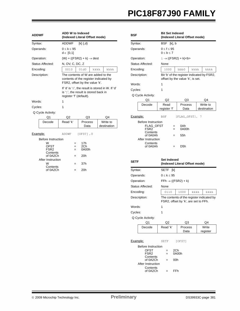
© 2009 Microchip Technology Inc. Preliminary DS39933C-page 381
PIC18F87J90 FAMILY
ADDWF ADD W to Indexed(Indexed Literal Offset mode)
Syntax: ADDWF [k] ,d
Operands: 0 ≤ k ≤ 95d ∈ [0,1]
Operation: (W) + ((FSR2) + k) → dest
Status Affected: N, OV, C, DC, Z
Encoding: 0010 01d0 kkkk kkkk
Description: The contents of W are added to the contents of the register indicated by FSR2, offset by the value ‘k’.
If ‘d’ is ‘0’, the result is stored in W. If ‘d’ is ‘1’, the result is stored back in register ‘f’ (default).
Words: 1
Cycles: 1
Q Cycle Activity:Q1 Q2 Q3 Q4
Decode Read ‘k’ Process Data
Write todestination
Example: ADDWF [OFST] ,0
Before InstructionW = 17hOFST = 2ChFSR2 = 0A00hContentsof 0A2Ch = 20h
After InstructionW = 37hContentsof 0A2Ch = 20h
BSF Bit Set Indexed (Indexed Literal Offset mode)
Syntax: BSF [k], b
Operands: 0 ≤ f ≤ 950 ≤ b ≤ 7
Operation: 1 → ((FSR2) + k)<b>
Status Affected: None
Encoding: 1000 bbb0 kkkk kkkk
Description: Bit ‘b’ of the register indicated by FSR2, offset by the value ‘k’, is set.
Words: 1
Cycles: 1
Q Cycle Activity:Q1 Q2 Q3 Q4
Decode Readregister ‘f’
Process Data
Write todestination
Example: BSF [FLAG_OFST], 7
Before InstructionFLAG_OFST = 0AhFSR2 = 0A00hContents of 0A0Ah = 55h
After InstructionContentsof 0A0Ah = D5h
SETF Set Indexed(Indexed Literal Offset mode)
Syntax: SETF [k]
Operands: 0 ≤ k ≤ 95
Operation: FFh → ((FSR2) + k)
Status Affected: None
Encoding: 0110 1000 kkkk kkkk
Description: The contents of the register indicated by FSR2, offset by ‘k’, are set to FFh.
Words: 1
Cycles: 1
Q Cycle Activity:Q1 Q2 Q3 Q4
Decode Read ‘k’ Process Data
Writeregister
Example: SETF [OFST]
Before InstructionOFST = 2ChFSR2 = 0A00hContentsof 0A2Ch = 00h
After InstructionContentsof 0A2Ch = FFh
PIC18F87J90 FAMILY
DS39933C-page 382 Preliminary © 2009 Microchip Technology Inc.
25.2.5 SPECIAL CONSIDERATIONS WITH MICROCHIP MPLAB® IDE TOOLS
The latest versions of Microchip’s software tools havebeen designed to fully support the extended instructionset for the PIC18F87J90 family family. This includesthe MPLAB C18 C Compiler, MPASM assemblylanguage and MPLAB Integrated DevelopmentEnvironment (IDE).
When selecting a target device for softwaredevelopment, MPLAB IDE will automatically set defaultConfiguration bits for that device. The default setting forthe XINST Configuration bit is ‘0’, disabling theextended instruction set and Indexed Literal OffsetAddressing. For proper execution of applicationsdeveloped to take advantage of the extendedinstruction set, XINST must be set duringprogramming.
To develop software for the extended instruction set,the user must enable support for the instructions andthe Indexed Addressing mode in their language tool(s).Depending on the environment being used, this may bedone in several ways:
• A menu option or dialog box within the environment that allows the user to configure the language tool and its settings for the project
• A command line option• A directive in the source code
These options vary between different compilers,assemblers and development environments. Users areencouraged to review the documentation accompany-ing their development systems for the appropriateinformation.
© 2009 Microchip Technology Inc. Preliminary DS39933C-page 383
PIC18F87J90 FAMILY
26.0 DEVELOPMENT SUPPORTThe PIC® microcontrollers are supported with a fullrange of hardware and software development tools:
• Integrated Development Environment- MPLAB® IDE Software
• Assemblers/Compilers/Linkers- MPASMTM Assembler- MPLAB C18 and MPLAB C30 C Compilers- MPLINKTM Object Linker/
MPLIBTM Object Librarian- MPLAB ASM30 Assembler/Linker/Library
• Simulators- MPLAB SIM Software Simulator
• Emulators- MPLAB ICE 2000 In-Circuit Emulator- MPLAB REAL ICE™ In-Circuit Emulator
• In-Circuit Debugger- MPLAB ICD 2
• Device Programmers- PICSTART® Plus Development Programmer- MPLAB PM3 Device Programmer- PICkit™ 2 Development Programmer
• Low-Cost Demonstration and Development Boards and Evaluation Kits
26.1 MPLAB Integrated Development Environment Software
The MPLAB IDE software brings an ease of softwaredevelopment previously unseen in the 8/16-bit micro-controller market. The MPLAB IDE is a Windows®
operating system-based application that contains:
• A single graphical interface to all debugging tools- Simulator- Programmer (sold separately)- Emulator (sold separately)- In-Circuit Debugger (sold separately)
• A full-featured editor with color-coded context• A multiple project manager• Customizable data windows with direct edit of
contents• High-level source code debugging• Visual device initializer for easy register
initialization• Mouse over variable inspection• Drag and drop variables from source to watch
windows• Extensive on-line help• Integration of select third party tools, such as
HI-TECH Software C Compilers and IAR C Compilers
The MPLAB IDE allows you to:
• Edit your source files (either assembly or C)• One touch assemble (or compile) and download
to PIC MCU emulator and simulator tools (automatically updates all project information)
• Debug using:- Source files (assembly or C)- Mixed assembly and C- Machine code
MPLAB IDE supports multiple debugging tools in asingle development paradigm, from the cost-effectivesimulators, through low-cost in-circuit debuggers, tofull-featured emulators. This eliminates the learningcurve when upgrading to tools with increased flexibilityand power.
PIC18F87J90 FAMILY
DS39933C-page 384 Preliminary © 2009 Microchip Technology Inc.
26.2 MPASM AssemblerThe MPASM Assembler is a full-featured, universalmacro assembler for all PIC MCUs.
The MPASM Assembler generates relocatable objectfiles for the MPLINK Object Linker, Intel® standard HEXfiles, MAP files to detail memory usage and symbolreference, absolute LST files that contain source linesand generated machine code and COFF files fordebugging.
The MPASM Assembler features include:
• Integration into MPLAB IDE projects• User-defined macros to streamline
assembly code• Conditional assembly for multi-purpose
source files• Directives that allow complete control over the
assembly process
26.3 MPLAB C18 and MPLAB C30 C Compilers
The MPLAB C18 and MPLAB C30 Code DevelopmentSystems are complete ANSI C compilers forMicrochip’s PIC18 and PIC24 families of microcon-trollers and the dsPIC30 and dsPIC33 family of digitalsignal controllers. These compilers provide powerfulintegration capabilities, superior code optimization andease of use not found with other compilers.
For easy source level debugging, the compilers providesymbol information that is optimized to the MPLAB IDEdebugger.
26.4 MPLINK Object Linker/MPLIB Object Librarian
The MPLINK Object Linker combines relocatableobjects created by the MPASM Assembler and theMPLAB C18 C Compiler. It can link relocatable objectsfrom precompiled libraries, using directives from alinker script.
The MPLIB Object Librarian manages the creation andmodification of library files of precompiled code. Whena routine from a library is called from a source file, onlythe modules that contain that routine will be linked inwith the application. This allows large libraries to beused efficiently in many different applications.
The object linker/library features include:
• Efficient linking of single libraries instead of many smaller files
• Enhanced code maintainability by grouping related modules together
• Flexible creation of libraries with easy module listing, replacement, deletion and extraction
26.5 MPLAB ASM30 Assembler, Linker and Librarian
MPLAB ASM30 Assembler produces relocatablemachine code from symbolic assembly language fordsPIC30F devices. MPLAB C30 C Compiler uses theassembler to produce its object file. The assemblergenerates relocatable object files that can then bearchived or linked with other relocatable object files andarchives to create an executable file. Notable featuresof the assembler include:
• Support for the entire dsPIC30F instruction set• Support for fixed-point and floating-point data• Command line interface• Rich directive set• Flexible macro language• MPLAB IDE compatibility
26.6 MPLAB SIM Software SimulatorThe MPLAB SIM Software Simulator allows codedevelopment in a PC-hosted environment by simulat-ing the PIC MCUs and dsPIC® DSCs on an instructionlevel. On any given instruction, the data areas can beexamined or modified and stimuli can be applied froma comprehensive stimulus controller. Registers can belogged to files for further run-time analysis. The tracebuffer and logic analyzer display extend the power ofthe simulator to record and track program execution,actions on I/O, most peripherals and internal registers.
The MPLAB SIM Software Simulator fully supportssymbolic debugging using the MPLAB C18 andMPLAB C30 C Compilers, and the MPASM andMPLAB ASM30 Assemblers. The software simulatoroffers the flexibility to develop and debug code outsideof the hardware laboratory environment, making it anexcellent, economical software development tool.
© 2009 Microchip Technology Inc. Preliminary DS39933C-page 385
PIC18F87J90 FAMILY26.7 MPLAB ICE 2000
High-Performance In-Circuit Emulator
The MPLAB ICE 2000 In-Circuit Emulator is intendedto provide the product development engineer with acomplete microcontroller design tool set for PICmicrocontrollers. Software control of the MPLAB ICE2000 In-Circuit Emulator is advanced by the MPLABIntegrated Development Environment, which allowsediting, building, downloading and source debuggingfrom a single environment.
The MPLAB ICE 2000 is a full-featured emulatorsystem with enhanced trace, trigger and data monitor-ing features. Interchangeable processor modules allowthe system to be easily reconfigured for emulation ofdifferent processors. The architecture of the MPLABICE 2000 In-Circuit Emulator allows expansion tosupport new PIC microcontrollers.
The MPLAB ICE 2000 In-Circuit Emulator system hasbeen designed as a real-time emulation system withadvanced features that are typically found on moreexpensive development tools. The PC platform andMicrosoft® Windows® 32-bit operating system werechosen to best make these features available in asimple, unified application.
26.8 MPLAB REAL ICE In-Circuit Emulator System
MPLAB REAL ICE In-Circuit Emulator System isMicrochip’s next generation high-speed emulator forMicrochip Flash DSC and MCU devices. It debugs andprograms PIC® Flash MCUs and dsPIC® Flash DSCswith the easy-to-use, powerful graphical user interface ofthe MPLAB Integrated Development Environment (IDE),included with each kit.
The MPLAB REAL ICE probe is connected to the designengineer’s PC using a high-speed USB 2.0 interface andis connected to the target with either a connectorcompatible with the popular MPLAB ICD 2 system(RJ11) or with the new high-speed, noise tolerant, Low-Voltage Differential Signal (LVDS) interconnection(CAT5).
MPLAB REAL ICE is field upgradeable through futurefirmware downloads in MPLAB IDE. In upcomingreleases of MPLAB IDE, new devices will be supported,and new features will be added, such as software break-points and assembly code trace. MPLAB REAL ICEoffers significant advantages over competitive emulatorsincluding low-cost, full-speed emulation, real-timevariable watches, trace analysis, complex breakpoints, aruggedized probe interface and long (up to three meters)interconnection cables.
26.9 MPLAB ICD 2 In-Circuit DebuggerMicrochip’s In-Circuit Debugger, MPLAB ICD 2, is apowerful, low-cost, run-time development tool,connecting to the host PC via an RS-232 or high-speedUSB interface. This tool is based on the Flash PICMCUs and can be used to develop for these and otherPIC MCUs and dsPIC DSCs. The MPLAB ICD 2 utilizesthe in-circuit debugging capability built into the Flashdevices. This feature, along with Microchip’s In-CircuitSerial ProgrammingTM (ICSPTM) protocol, offers cost-effective, in-circuit Flash debugging from the graphicaluser interface of the MPLAB Integrated DevelopmentEnvironment. This enables a designer to develop anddebug source code by setting breakpoints, single step-ping and watching variables, and CPU status andperipheral registers. Running at full speed enablestesting hardware and applications in real time. MPLABICD 2 also serves as a development programmer forselected PIC devices.
26.10 MPLAB PM3 Device ProgrammerThe MPLAB PM3 Device Programmer is a universal,CE compliant device programmer with programmablevoltage verification at VDDMIN and VDDMAX formaximum reliability. It features a large LCD display(128 x 64) for menus and error messages and a modu-lar, detachable socket assembly to support variouspackage types. The ICSP™ cable assembly is includedas a standard item. In Stand-Alone mode, the MPLABPM3 Device Programmer can read, verify and programPIC devices without a PC connection. It can also setcode protection in this mode. The MPLAB PM3connects to the host PC via an RS-232 or USB cable.The MPLAB PM3 has high-speed communications andoptimized algorithms for quick programming of largememory devices and incorporates an SD/MMC card forfile storage and secure data applications.

PIC18F87J90 FAMILY
DS39933C-page 386 Preliminary © 2009 Microchip Technology Inc.
26.11 PICSTART Plus Development Programmer
The PICSTART Plus Development Programmer is aneasy-to-use, low-cost, prototype programmer. Itconnects to the PC via a COM (RS-232) port. MPLABIntegrated Development Environment software makesusing the programmer simple and efficient. ThePICSTART Plus Development Programmer supportsmost PIC devices in DIP packages up to 40 pins.Larger pin count devices, such as the PIC16C92X andPIC17C76X, may be supported with an adapter socket.The PICSTART Plus Development Programmer is CEcompliant.
26.12 PICkit 2 Development ProgrammerThe PICkit™ 2 Development Programmer is a low-costprogrammer and selected Flash device debugger withan easy-to-use interface for programming many ofMicrochip’s baseline, mid-range and PIC18F families ofFlash memory microcontrollers. The PICkit 2 Starter Kitincludes a prototyping development board, twelvesequential lessons, software and HI-TECH’s PICC™Lite C compiler, and is designed to help get up to speedquickly using PIC® microcontrollers. The kit provideseverything needed to program, evaluate and developapplications using Microchip’s powerful, mid-rangeFlash memory family of microcontrollers.
26.13 Demonstration, Development and Evaluation Boards
A wide variety of demonstration, development andevaluation boards for various PIC MCUs and dsPICDSCs allows quick application development on fully func-tional systems. Most boards include prototyping areas foradding custom circuitry and provide application firmwareand source code for examination and modification.
The boards support a variety of features, including LEDs,temperature sensors, switches, speakers, RS-232interfaces, LCD displays, potentiometers and additionalEEPROM memory.
The demonstration and development boards can beused in teaching environments, for prototyping customcircuits and for learning about various microcontrollerapplications.
In addition to the PICDEM™ and dsPICDEM™ demon-stration/development board series of circuits, Microchiphas a line of evaluation kits and demonstration softwarefor analog filter design, KEELOQ® security ICs, CAN,IrDA®, PowerSmart battery management, SEEVAL®
evaluation system, Sigma-Delta ADC, flow ratesensing, plus many more.
Check the Microchip web page (www.microchip.com)for the complete list of demonstration, developmentand evaluation kits.
© 2009 Microchip Technology Inc. Preliminary DS39933C-page 387
PIC18F87J90 FAMILY
27.0 ELECTRICAL CHARACTERISTICS
Absolute Maximum Ratings(†) Ambient temperature under bias............................................................................................................ .-40°C to +100°C
Storage temperature .............................................................................................................................. -65°C to +150°C
Voltage on any digital only I/O pin or MCLR with respect to VSS (except VDD) ........................................... -0.3V to 6.0V
Voltage on any combined digital and analog pin with respect to VSS (except VDD and MCLR)...... -0.3V to (VDD + 0.3V)
Voltage on VDDCORE with respect to VSS................................................................................................... -0.3V to 2.75V
Voltage on VDD with respect to VSS ........................................................................................................... -0.3V to 3.6V
Total power dissipation (Note 1) ...............................................................................................................................1.0W
Maximum current out of VSS pin ...........................................................................................................................300 mA
Maximum current into VDD pin ..............................................................................................................................250 mA
Maximum output current sunk by PORTA<7:6> and any PORTB and PORTC I/O pins.........................................25 mA
Maximum output current sunk by any PORTD, PORTE and PORTJ I/O pins ..........................................................8 mA
Maximum output current sunk by PORTA<5:0> and any PORTF, PORTG and PORTH I/O pins ............................2 mA
Maximum output current sourced by PORTA<7:6> and any PORTB and PORTC I/O pins ...................................25 mA
Maximum output current sourced by any PORTD, PORTE and PORTJ I/O pins .....................................................8 mA
Maximum output current sourced by PORTA<5:0> and any PORTF, PORTG and PORTH I/O pins .......................2 mA
Maximum current sunk by all ports combined.......................................................................................................200 mA
Note 1: Power dissipation is calculated as follows: Pdis = VDD x IDD – ∑ IOH + ∑ (VDD – VOH) x IOH + ∑(VOL x IOL)
† NOTICE: Stresses above those listed under “Absolute Maximum Ratings” may cause permanent damage to the device. This is a stress rating only and functional operation of the device at those or any other conditions above those indicated in the operation listings of this specification is not implied. Exposure to maximum rating conditions for extended periods may affect device reliability.
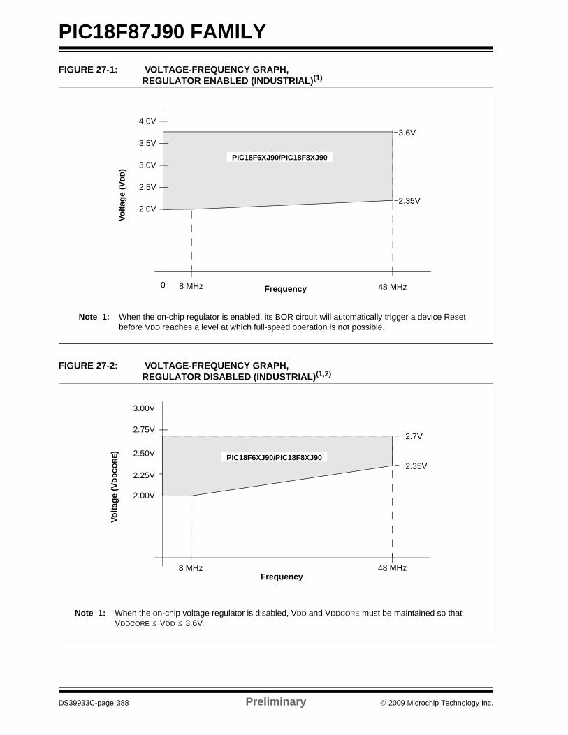
PIC18F87J90 FAMILY
DS39933C-page 388 Preliminary © 2009 Microchip Technology Inc.
FIGURE 27-1: VOLTAGE-FREQUENCY GRAPH, REGULATOR ENABLED (INDUSTRIAL)(1)
FIGURE 27-2: VOLTAGE-FREQUENCY GRAPH, REGULATOR DISABLED (INDUSTRIAL)(1,2)
Frequency
Volta
ge (V
DD
)4.0V
2.0V
48 MHz
3.5V
3.0V
2.5V
3.6V
2.35V
0
Note 1: When the on-chip regulator is enabled, its BOR circuit will automatically trigger a device Reset before VDD reaches a level at which full-speed operation is not possible.
8 MHz
PIC18F6XJ90/PIC18F8XJ90
Frequency
Volta
ge (V
DD
CO
RE)
3.00V
2.00V
48 MHz
2.75V
2.50V
2.25V
2.7V
8 MHz
2.35V
Note 1: When the on-chip voltage regulator is disabled, VDD and VDDCORE must be maintained so that VDDCORE ≤ VDD ≤ 3.6V.
PIC18F6XJ90/PIC18F8XJ90
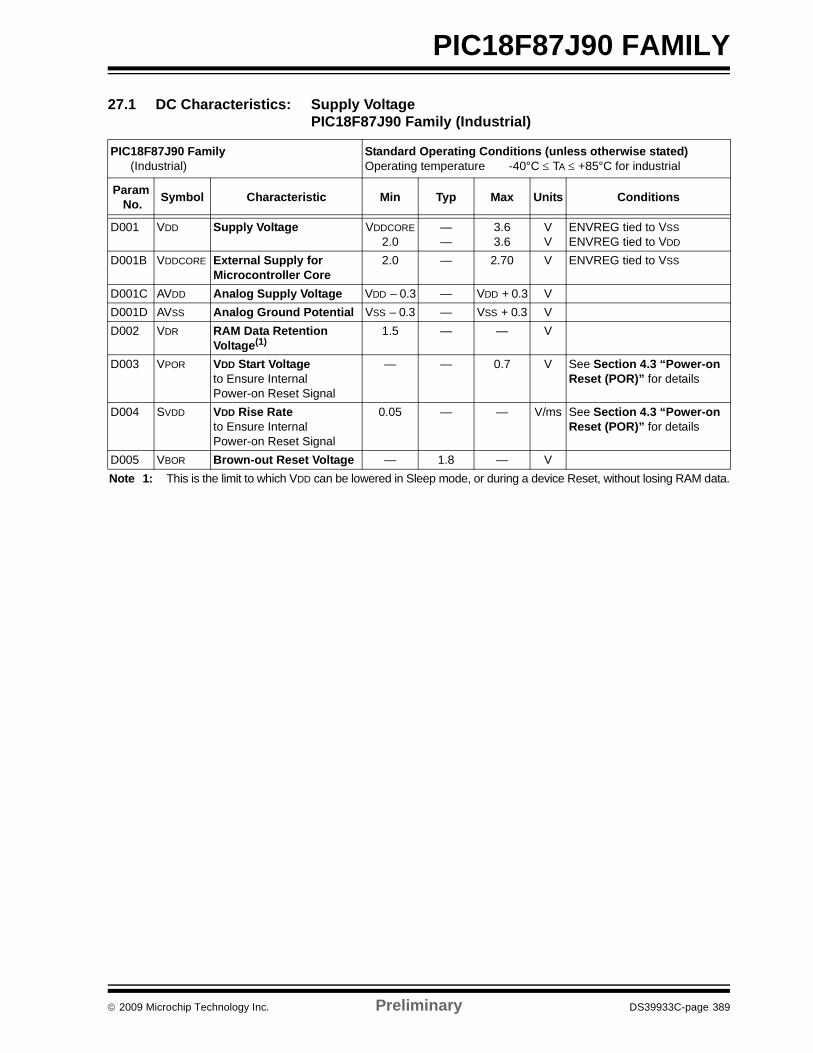
© 2009 Microchip Technology Inc. Preliminary DS39933C-page 389
PIC18F87J90 FAMILY
27.1 DC Characteristics: Supply VoltagePIC18F87J90 Family (Industrial)
PIC18F87J90 Family (Industrial)
Standard Operating Conditions (unless otherwise stated)Operating temperature -40°C ≤ TA ≤ +85°C for industrial
Param No. Symbol Characteristic Min Typ Max Units Conditions
D001 VDD Supply Voltage VDDCORE2.0
——
3.63.6
VV
ENVREG tied to VSSENVREG tied to VDD
D001B VDDCORE External Supply for Microcontroller Core
2.0 — 2.70 V ENVREG tied to VSS
D001C AVDD Analog Supply Voltage VDD – 0.3 — VDD + 0.3 VD001D AVSS Analog Ground Potential VSS – 0.3 — VSS + 0.3 VD002 VDR RAM Data Retention
Voltage(1)1.5 — — V
D003 VPOR VDD Start Voltage to Ensure Internal Power-on Reset Signal
— — 0.7 V See Section 4.3 “Power-on Reset (POR)” for details
D004 SVDD VDD Rise Rateto Ensure Internal Power-on Reset Signal
0.05 — — V/ms See Section 4.3 “Power-on Reset (POR)” for details
D005 VBOR Brown-out Reset Voltage — 1.8 — VNote 1: This is the limit to which VDD can be lowered in Sleep mode, or during a device Reset, without losing RAM data.
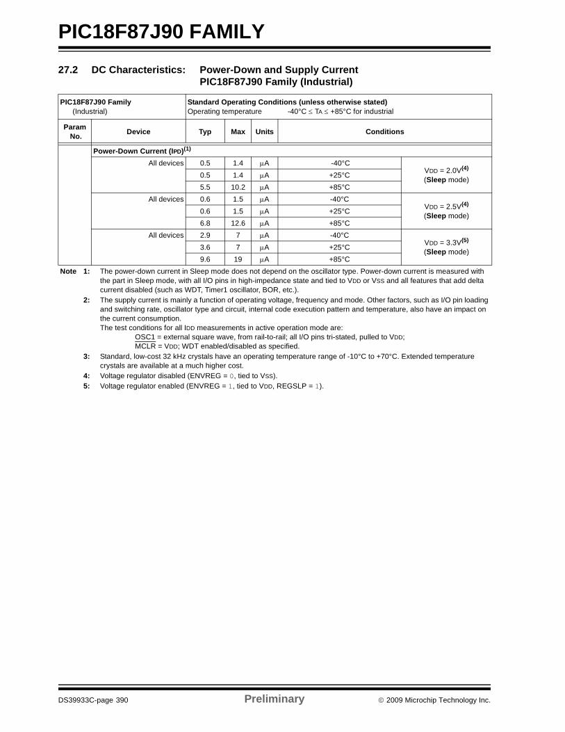
PIC18F87J90 FAMILY
DS39933C-page 390 Preliminary © 2009 Microchip Technology Inc.
27.2 DC Characteristics: Power-Down and Supply CurrentPIC18F87J90 Family (Industrial)
PIC18F87J90 Family (Industrial)
Standard Operating Conditions (unless otherwise stated)Operating temperature -40°C ≤ TA ≤ +85°C for industrial
Param No. Device Typ Max Units Conditions
Power-Down Current (IPD)(1)
All devices 0.5 1.4 μA -40°CVDD = 2.0V(4)
(Sleep mode)0.5 1.4 μA +25°C5.5 10.2 μA +85°C
All devices 0.6 1.5 μA -40°CVDD = 2.5V(4)
(Sleep mode)0.6 1.5 μA +25°C6.8 12.6 μA +85°C
All devices 2.9 7 μA -40°CVDD = 3.3V(5)
(Sleep mode)3.6 7 μA +25°C9.6 19 μA +85°C
Note 1: The power-down current in Sleep mode does not depend on the oscillator type. Power-down current is measured with the part in Sleep mode, with all I/O pins in high-impedance state and tied to VDD or VSS and all features that add delta current disabled (such as WDT, Timer1 oscillator, BOR, etc.).
2: The supply current is mainly a function of operating voltage, frequency and mode. Other factors, such as I/O pin loading and switching rate, oscillator type and circuit, internal code execution pattern and temperature, also have an impact on the current consumption.The test conditions for all IDD measurements in active operation mode are:
OSC1 = external square wave, from rail-to-rail; all I/O pins tri-stated, pulled to VDD;MCLR = VDD; WDT enabled/disabled as specified.
3: Standard, low-cost 32 kHz crystals have an operating temperature range of -10°C to +70°C. Extended temperature crystals are available at a much higher cost.
4: Voltage regulator disabled (ENVREG = 0, tied to VSS).5: Voltage regulator enabled (ENVREG = 1, tied to VDD, REGSLP = 1).
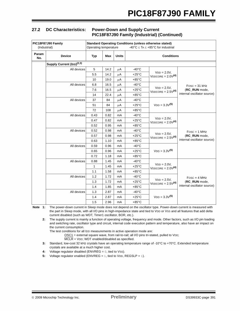
© 2009 Microchip Technology Inc. Preliminary DS39933C-page 391
PIC18F87J90 FAMILY
Supply Current (IDD)(2,3)
All devices 5 14.2 μA -40°CVDD = 2.0V,
VDDCORE = 2.0V(4)
FOSC = 31 kHz(RC_RUN mode,
internal oscillator source)
5.5 14.2 μA +25°C 10 19.0 μA +85°C
All devices 6.8 16.5 μA -40°CVDD = 2.5V,
VDDCORE = 2.5V(4)7.6 16.5 μA +25°C 14 22.4 μA +85°C
All devices 37 84 μA -40°C51 84 μA +25°C VDD = 3.3V(5)
72 108 μA +85°CAll devices 0.43 0.82 mA -40°C
VDD = 2.0V,VDDCORE = 2.0V(4)
FOSC = 1 MHz(RC_RUN mode,
internal oscillator source)
0.47 0.82 mA +25°C 0.52 0.95 mA +85°C
All devices 0.52 0.98 mA -40°CVDD = 2.5V,
VDDCORE = 2.5V(4)0.57 0.98 mA +25°C 0.63 1.10 mA +85°C
All devices 0.59 0.96 mA -40°C0.65 0.96 mA +25°C VDD = 3.3V(5)
0.72 1.18 mA +85°CAll devices 0.88 1.45 mA -40°C
VDD = 2.0V,VDDCORE = 2.0V(4)
FOSC = 4 MHz(RC_RUN mode,
internal oscillator source)
1 1.45 mA +25°C 1.1 1.58 mA +85°C
All devices 1.2 1.72 mA -40°CVDD = 2.5V,
VDDCORE = 2.5V(4)1.3 1.72 mA +25°C 1.4 1.85 mA +85°C
All devices 1.3 2.87 mA -40°C1.4 2.87 mA +25°C VDD = 3.3V(5)
1.5 2.96 mA +85°C
27.2 DC Characteristics: Power-Down and Supply CurrentPIC18F87J90 Family (Industrial) (Continued)
PIC18F87J90 Family (Industrial)
Standard Operating Conditions (unless otherwise stated)Operating temperature -40°C ≤ TA ≤ +85°C for industrial
Param No. Device Typ Max Units Conditions
Note 1: The power-down current in Sleep mode does not depend on the oscillator type. Power-down current is measured with the part in Sleep mode, with all I/O pins in high-impedance state and tied to VDD or VSS and all features that add delta current disabled (such as WDT, Timer1 oscillator, BOR, etc.).
2: The supply current is mainly a function of operating voltage, frequency and mode. Other factors, such as I/O pin loading and switching rate, oscillator type and circuit, internal code execution pattern and temperature, also have an impact on the current consumption.The test conditions for all IDD measurements in active operation mode are:
OSC1 = external square wave, from rail-to-rail; all I/O pins tri-stated, pulled to VDD;MCLR = VDD; WDT enabled/disabled as specified.
3: Standard, low-cost 32 kHz crystals have an operating temperature range of -10°C to +70°C. Extended temperature crystals are available at a much higher cost.
4: Voltage regulator disabled (ENVREG = 0, tied to VSS).5: Voltage regulator enabled (ENVREG = 1, tied to VDD, REGSLP = 1).
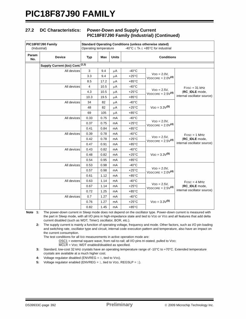
PIC18F87J90 FAMILY
DS39933C-page 392 Preliminary © 2009 Microchip Technology Inc.
Supply Current (IDD) Cont.(2,3)
All devices 3 9.4 μA -40°CVDD = 2.0V,
VDDCORE = 2.0V(4)
FOSC = 31 kHz(RC_IDLE mode,
internal oscillator source)
3.3 9.4 μA +25°C 8.5 17.2 μA +85°C
All devices 4 10.5 μA -40°CVDD = 2.5V,
VDDCORE = 2.5V(4)4.3 10.5 μA +25°C 10.3 19.5 μA +85°C
All devices 34 82 μA -40°C48 82 μA +25°C VDD = 3.3V(5)
69 105 μA +85°CAll devices 0.33 0.75 mA -40°C
VDD = 2.0V,VDDCORE = 2.0V(4)
FOSC = 1 MHz(RC_IDLE mode,
internal oscillator source)
0.37 0.75 mA +25°C 0.41 0.84 mA +85°C
All devices 0.39 0.78 mA -40°CVDD = 2.5V,
VDDCORE = 2.5V(4)0.42 0.78 mA +25°C 0.47 0.91 mA +85°C
All devices 0.43 0.82 mA -40°C0.48 0.82 mA +25°C VDD = 3.3V(5)
0.54 0.95 mA +85°CAll devices 0.53 0.98 mA -40°C
VDD = 2.0V,VDDCORE = 2.0V(4)
FOSC = 4 MHz(RC_IDLE mode,
internal oscillator source)
0.57 0.98 mA +25°C 0.61 1.12 mA +85°C
All devices 0.63 1.14 mA -40°CVDD = 2.5V,
VDDCORE = 2.5V(4)0.67 1.14 mA +25°C 0.72 1.25 mA +85°C
All devices 0.7 1.27 mA -40°C0.76 1.27 mA +25°C VDD = 3.3V(5)
0.82 1.45 mA +85°C
27.2 DC Characteristics: Power-Down and Supply CurrentPIC18F87J90 Family (Industrial) (Continued)
PIC18F87J90 Family (Industrial)
Standard Operating Conditions (unless otherwise stated)Operating temperature -40°C ≤ TA ≤ +85°C for industrial
Param No. Device Typ Max Units Conditions
Note 1: The power-down current in Sleep mode does not depend on the oscillator type. Power-down current is measured with the part in Sleep mode, with all I/O pins in high-impedance state and tied to VDD or VSS and all features that add delta current disabled (such as WDT, Timer1 oscillator, BOR, etc.).
2: The supply current is mainly a function of operating voltage, frequency and mode. Other factors, such as I/O pin loading and switching rate, oscillator type and circuit, internal code execution pattern and temperature, also have an impact on the current consumption.The test conditions for all IDD measurements in active operation mode are:
OSC1 = external square wave, from rail-to-rail; all I/O pins tri-stated, pulled to VDD;MCLR = VDD; WDT enabled/disabled as specified.
3: Standard, low-cost 32 kHz crystals have an operating temperature range of -10°C to +70°C. Extended temperature crystals are available at a much higher cost.
4: Voltage regulator disabled (ENVREG = 0, tied to VSS).5: Voltage regulator enabled (ENVREG = 1, tied to VDD, REGSLP = 1).
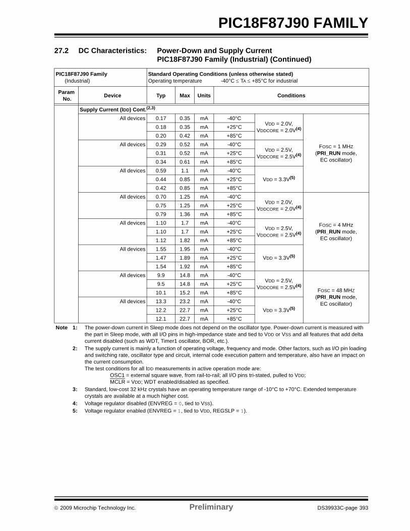
© 2009 Microchip Technology Inc. Preliminary DS39933C-page 393
PIC18F87J90 FAMILY
Supply Current (IDD) Cont.(2,3)
All devices 0.17 0.35 mA -40°CVDD = 2.0V,
VDDCORE = 2.0V(4)
FOSC = 1 MHZ(PRI_RUN mode,
EC oscillator)
0.18 0.35 mA +25°C 0.20 0.42 mA +85°C
All devices 0.29 0.52 mA -40°CVDD = 2.5V,
VDDCORE = 2.5V(4)0.31 0.52 mA +25°C 0.34 0.61 mA +85°C
All devices 0.59 1.1 mA -40°C0.44 0.85 mA +25°C VDD = 3.3V(5)
0.42 0.85 mA +85°CAll devices 0.70 1.25 mA -40°C
VDD = 2.0V,VDDCORE = 2.0V(4)
FOSC = 4 MHz(PRI_RUN mode,
EC oscillator)
0.75 1.25 mA +25°C 0.79 1.36 mA +85°C
All devices 1.10 1.7 mA -40°CVDD = 2.5V,
VDDCORE = 2.5V(4)1.10 1.7 mA +25°C 1.12 1.82 mA +85°C
All devices 1.55 1.95 mA -40°C1.47 1.89 mA +25°C VDD = 3.3V(5)
1.54 1.92 mA +85°CAll devices 9.9 14.8 mA -40°C
VDD = 2.5V,VDDCORE = 2.5V(4)
FOSC = 48 MHZ(PRI_RUN mode,
EC oscillator)
9.5 14.8 mA +25°C 10.1 15.2 mA +85°C
All devices 13.3 23.2 mA -40°C12.2 22.7 mA +25°C VDD = 3.3V(5)
12.1 22.7 mA +85°C
27.2 DC Characteristics: Power-Down and Supply CurrentPIC18F87J90 Family (Industrial) (Continued)
PIC18F87J90 Family (Industrial)
Standard Operating Conditions (unless otherwise stated)Operating temperature -40°C ≤ TA ≤ +85°C for industrial
Param No. Device Typ Max Units Conditions
Note 1: The power-down current in Sleep mode does not depend on the oscillator type. Power-down current is measured with the part in Sleep mode, with all I/O pins in high-impedance state and tied to VDD or VSS and all features that add delta current disabled (such as WDT, Timer1 oscillator, BOR, etc.).
2: The supply current is mainly a function of operating voltage, frequency and mode. Other factors, such as I/O pin loading and switching rate, oscillator type and circuit, internal code execution pattern and temperature, also have an impact on the current consumption.The test conditions for all IDD measurements in active operation mode are:
OSC1 = external square wave, from rail-to-rail; all I/O pins tri-stated, pulled to VDD;MCLR = VDD; WDT enabled/disabled as specified.
3: Standard, low-cost 32 kHz crystals have an operating temperature range of -10°C to +70°C. Extended temperature crystals are available at a much higher cost.
4: Voltage regulator disabled (ENVREG = 0, tied to VSS).5: Voltage regulator enabled (ENVREG = 1, tied to VDD, REGSLP = 1).
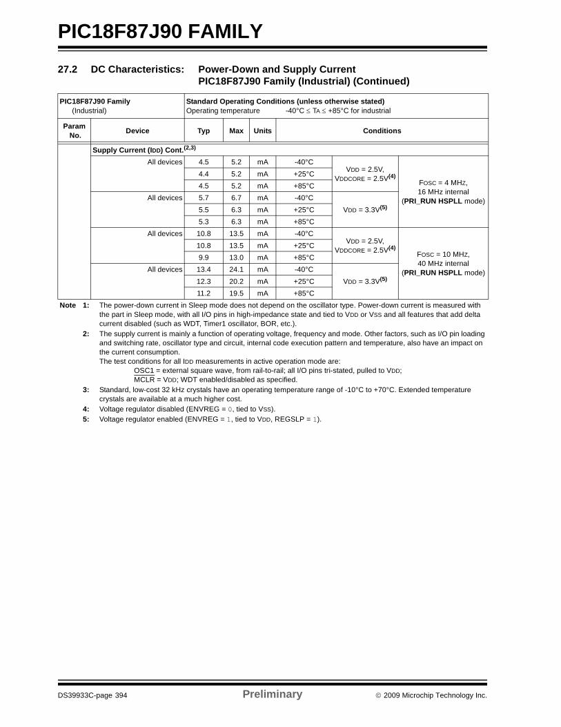
PIC18F87J90 FAMILY
DS39933C-page 394 Preliminary © 2009 Microchip Technology Inc.
Supply Current (IDD) Cont.(2,3)
All devices 4.5 5.2 mA -40°CVDD = 2.5V,
VDDCORE = 2.5V(4)FOSC = 4 MHZ,16 MHz internal
(PRI_RUN HSPLL mode)
4.4 5.2 mA +25°C4.5 5.2 mA +85°C
All devices 5.7 6.7 mA -40°CVDD = 3.3V(5)5.5 6.3 mA +25°C
5.3 6.3 mA +85°CAll devices 10.8 13.5 mA -40°C
VDD = 2.5V,VDDCORE = 2.5V(4)
FOSC = 10 MHZ,40 MHz internal
(PRI_RUN HSPLL mode)
10.8 13.5 mA +25°C9.9 13.0 mA +85°C
All devices 13.4 24.1 mA -40°CVDD = 3.3V(5)12.3 20.2 mA +25°C
11.2 19.5 mA +85°C
27.2 DC Characteristics: Power-Down and Supply CurrentPIC18F87J90 Family (Industrial) (Continued)
PIC18F87J90 Family (Industrial)
Standard Operating Conditions (unless otherwise stated)Operating temperature -40°C ≤ TA ≤ +85°C for industrial
Param No. Device Typ Max Units Conditions
Note 1: The power-down current in Sleep mode does not depend on the oscillator type. Power-down current is measured with the part in Sleep mode, with all I/O pins in high-impedance state and tied to VDD or VSS and all features that add delta current disabled (such as WDT, Timer1 oscillator, BOR, etc.).
2: The supply current is mainly a function of operating voltage, frequency and mode. Other factors, such as I/O pin loading and switching rate, oscillator type and circuit, internal code execution pattern and temperature, also have an impact on the current consumption.The test conditions for all IDD measurements in active operation mode are:
OSC1 = external square wave, from rail-to-rail; all I/O pins tri-stated, pulled to VDD;MCLR = VDD; WDT enabled/disabled as specified.
3: Standard, low-cost 32 kHz crystals have an operating temperature range of -10°C to +70°C. Extended temperature crystals are available at a much higher cost.
4: Voltage regulator disabled (ENVREG = 0, tied to VSS).5: Voltage regulator enabled (ENVREG = 1, tied to VDD, REGSLP = 1).
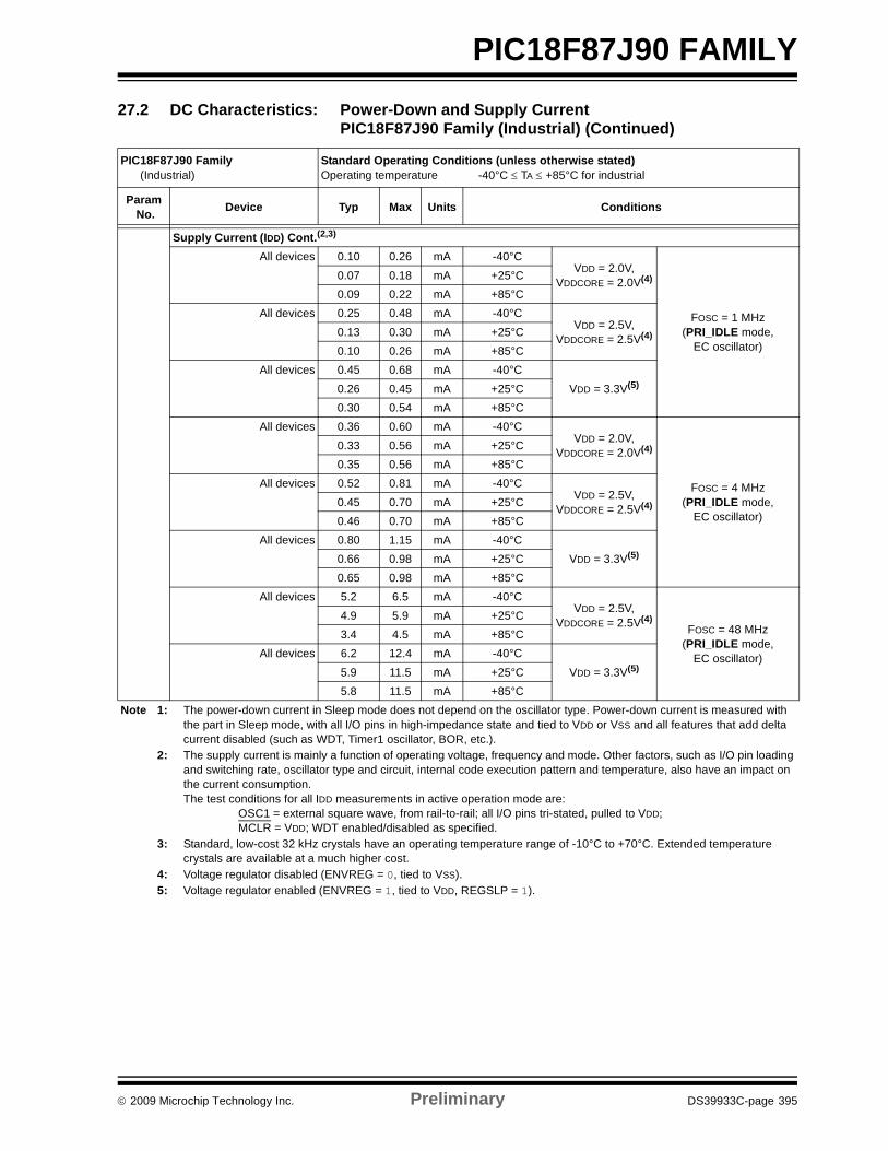
© 2009 Microchip Technology Inc. Preliminary DS39933C-page 395
PIC18F87J90 FAMILY
Supply Current (IDD) Cont.(2,3)
All devices 0.10 0.26 mA -40°CVDD = 2.0V,
VDDCORE = 2.0V(4)
FOSC = 1 MHz(PRI_IDLE mode,
EC oscillator)
0.07 0.18 mA +25°C 0.09 0.22 mA +85°C
All devices 0.25 0.48 mA -40°CVDD = 2.5V,
VDDCORE = 2.5V(4)0.13 0.30 mA +25°C 0.10 0.26 mA +85°C
All devices 0.45 0.68 mA -40°C0.26 0.45 mA +25°C VDD = 3.3V(5)
0.30 0.54 mA +85°CAll devices 0.36 0.60 mA -40°C
VDD = 2.0V,VDDCORE = 2.0V(4)
FOSC = 4 MHz(PRI_IDLE mode,
EC oscillator)
0.33 0.56 mA +25°C 0.35 0.56 mA +85°C
All devices 0.52 0.81 mA -40°CVDD = 2.5V,
VDDCORE = 2.5V(4)0.45 0.70 mA +25°C 0.46 0.70 mA +85°C
All devices 0.80 1.15 mA -40°C0.66 0.98 mA +25°C VDD = 3.3V(5)
0.65 0.98 mA +85°CAll devices 5.2 6.5 mA -40°C
VDD = 2.5V,VDDCORE = 2.5V(4)
FOSC = 48 MHz(PRI_IDLE mode,
EC oscillator)
4.9 5.9 mA +25°C 3.4 4.5 mA +85°C
All devices 6.2 12.4 mA -40°C5.9 11.5 mA +25°C VDD = 3.3V(5)
5.8 11.5 mA +85°C
27.2 DC Characteristics: Power-Down and Supply CurrentPIC18F87J90 Family (Industrial) (Continued)
PIC18F87J90 Family (Industrial)
Standard Operating Conditions (unless otherwise stated)Operating temperature -40°C ≤ TA ≤ +85°C for industrial
Param No. Device Typ Max Units Conditions
Note 1: The power-down current in Sleep mode does not depend on the oscillator type. Power-down current is measured with the part in Sleep mode, with all I/O pins in high-impedance state and tied to VDD or VSS and all features that add delta current disabled (such as WDT, Timer1 oscillator, BOR, etc.).
2: The supply current is mainly a function of operating voltage, frequency and mode. Other factors, such as I/O pin loading and switching rate, oscillator type and circuit, internal code execution pattern and temperature, also have an impact on the current consumption.The test conditions for all IDD measurements in active operation mode are:
OSC1 = external square wave, from rail-to-rail; all I/O pins tri-stated, pulled to VDD;MCLR = VDD; WDT enabled/disabled as specified.
3: Standard, low-cost 32 kHz crystals have an operating temperature range of -10°C to +70°C. Extended temperature crystals are available at a much higher cost.
4: Voltage regulator disabled (ENVREG = 0, tied to VSS).5: Voltage regulator enabled (ENVREG = 1, tied to VDD, REGSLP = 1).
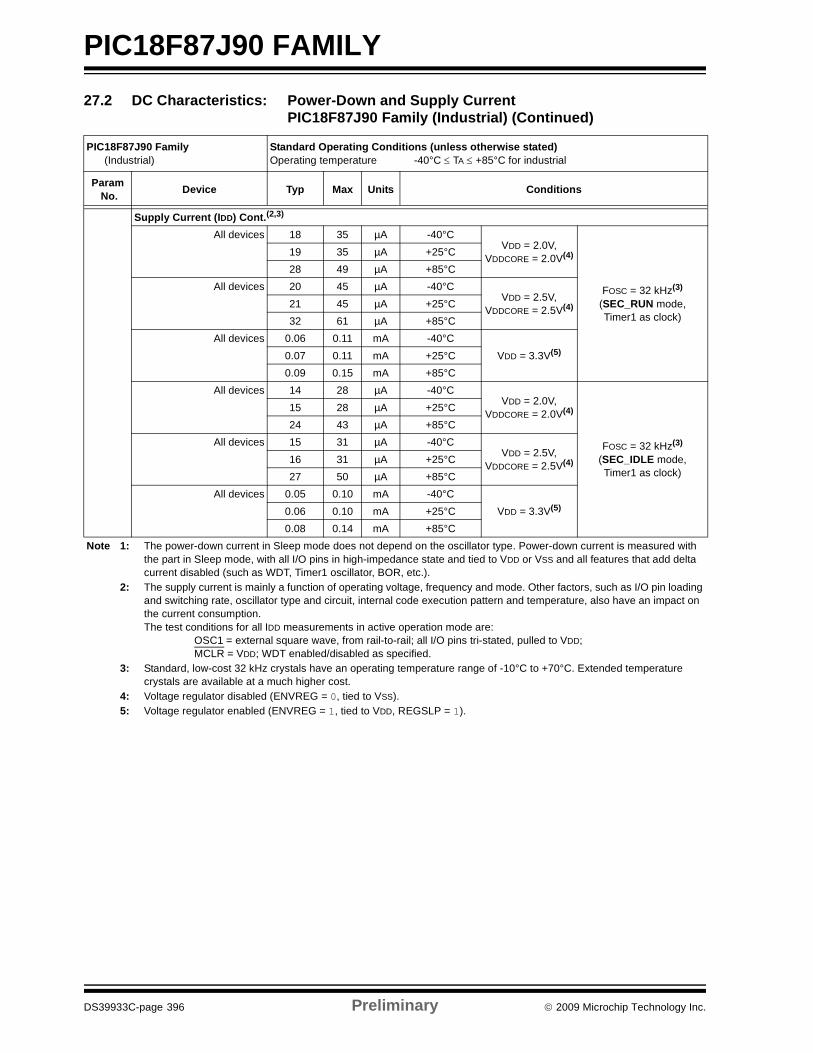
PIC18F87J90 FAMILY
DS39933C-page 396 Preliminary © 2009 Microchip Technology Inc.
Supply Current (IDD) Cont.(2,3)
All devices 18 35 µA -40°CVDD = 2.0V,
VDDCORE = 2.0V(4)
FOSC = 32 kHz(3)
(SEC_RUN mode, Timer1 as clock)
19 35 µA +25°C 28 49 µA +85°C
All devices 20 45 µA -40°CVDD = 2.5V,
VDDCORE = 2.5V(4)21 45 µA +25°C 32 61 µA +85°C
All devices 0.06 0.11 mA -40°C0.07 0.11 mA +25°C VDD = 3.3V(5)
0.09 0.15 mA +85°CAll devices 14 28 µA -40°C
VDD = 2.0V,VDDCORE = 2.0V(4)
FOSC = 32 kHz(3)
(SEC_IDLE mode, Timer1 as clock)
15 28 µA +25°C 24 43 µA +85°C
All devices 15 31 µA -40°CVDD = 2.5V,
VDDCORE = 2.5V(4)16 31 µA +25°C 27 50 µA +85°C
All devices 0.05 0.10 mA -40°C0.06 0.10 mA +25°C VDD = 3.3V(5)
0.08 0.14 mA +85°C
27.2 DC Characteristics: Power-Down and Supply CurrentPIC18F87J90 Family (Industrial) (Continued)
PIC18F87J90 Family (Industrial)
Standard Operating Conditions (unless otherwise stated)Operating temperature -40°C ≤ TA ≤ +85°C for industrial
Param No. Device Typ Max Units Conditions
Note 1: The power-down current in Sleep mode does not depend on the oscillator type. Power-down current is measured with the part in Sleep mode, with all I/O pins in high-impedance state and tied to VDD or VSS and all features that add delta current disabled (such as WDT, Timer1 oscillator, BOR, etc.).
2: The supply current is mainly a function of operating voltage, frequency and mode. Other factors, such as I/O pin loading and switching rate, oscillator type and circuit, internal code execution pattern and temperature, also have an impact on the current consumption.The test conditions for all IDD measurements in active operation mode are:
OSC1 = external square wave, from rail-to-rail; all I/O pins tri-stated, pulled to VDD;MCLR = VDD; WDT enabled/disabled as specified.
3: Standard, low-cost 32 kHz crystals have an operating temperature range of -10°C to +70°C. Extended temperature crystals are available at a much higher cost.
4: Voltage regulator disabled (ENVREG = 0, tied to VSS).5: Voltage regulator enabled (ENVREG = 1, tied to VDD, REGSLP = 1).
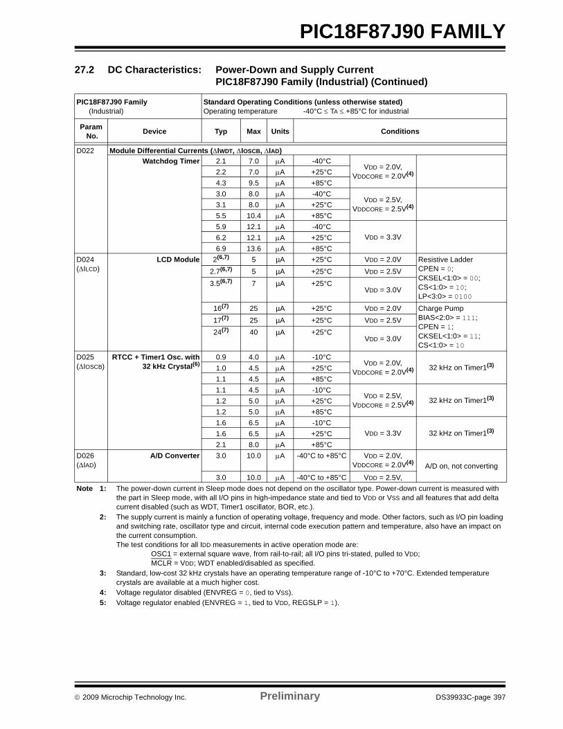
© 2009 Microchip Technology Inc. Preliminary DS39933C-page 397
PIC18F87J90 FAMILY
D022 Module Differential Currents (ΔIWDT, ΔIOSCB, ΔIAD)Watchdog Timer 2.1 7.0 μA -40°C
VDD = 2.0V,VDDCORE = 2.0V(4)2.2 7.0 μA +25°C
4.3 9.5 μA +85°C3.0 8.0 μA -40°C
VDD = 2.5V,VDDCORE = 2.5V(4)3.1 8.0 μA +25°C
5.5 10.4 μA +85°C5.9 12.1 μA -40°C
VDD = 3.3V6.2 12.1 μA +25°C6.9 13.6 μA +85°C
D024(ΔILCD)
LCD Module 2(6,7) 5 µA +25°C VDD = 2.0V Resistive LadderCPEN = 0;CKSEL<1:0> = 00; CS<1:0> = 10; LP<3:0> = 0100
2.7(6,7) 5 µA +25°C VDD = 2.5V3.5(6,7) 7 µA +25°C
VDD = 3.0V
16(7) 25 µA +25°C VDD = 2.0V Charge PumpBIAS<2:0> = 111;CPEN = 1;CKSEL<1:0> = 11;CS<1:0> = 10
17(7) 25 µA +25°C VDD = 2.5V24(7) 40 µA +25°C
VDD = 3.0V
D025(ΔIOSCB)
RTCC + Timer1 Osc. with32 kHz Crystal(6)
0.9 4.0 μA -10°CVDD = 2.0V,
VDDCORE = 2.0V(4) 32 kHz on Timer1(3)1.0 4.5 μA +25°C1.1 4.5 μA +85°C1.1 4.5 μA -10°C
VDD = 2.5V,VDDCORE = 2.5V(4) 32 kHz on Timer1(3)1.2 5.0 μA +25°C
1.2 5.0 μA +85°C1.6 6.5 μA -10°C
VDD = 3.3V 32 kHz on Timer1(3)1.6 6.5 μA +25°C2.1 8.0 μA +85°C
D026(ΔIAD)
A/D Converter 3.0 10.0 μA -40°C to +85°C VDD = 2.0V,VDDCORE = 2.0V(4) A/D on, not converting
3.0 10.0 μA -40°C to +85°C VDD = 2.5V,
27.2 DC Characteristics: Power-Down and Supply CurrentPIC18F87J90 Family (Industrial) (Continued)
PIC18F87J90 Family (Industrial)
Standard Operating Conditions (unless otherwise stated)Operating temperature -40°C ≤ TA ≤ +85°C for industrial
Param No. Device Typ Max Units Conditions
Note 1: The power-down current in Sleep mode does not depend on the oscillator type. Power-down current is measured with the part in Sleep mode, with all I/O pins in high-impedance state and tied to VDD or VSS and all features that add delta current disabled (such as WDT, Timer1 oscillator, BOR, etc.).
2: The supply current is mainly a function of operating voltage, frequency and mode. Other factors, such as I/O pin loading and switching rate, oscillator type and circuit, internal code execution pattern and temperature, also have an impact on the current consumption.The test conditions for all IDD measurements in active operation mode are:
OSC1 = external square wave, from rail-to-rail; all I/O pins tri-stated, pulled to VDD;MCLR = VDD; WDT enabled/disabled as specified.
3: Standard, low-cost 32 kHz crystals have an operating temperature range of -10°C to +70°C. Extended temperature crystals are available at a much higher cost.
4: Voltage regulator disabled (ENVREG = 0, tied to VSS).5: Voltage regulator enabled (ENVREG = 1, tied to VDD, REGSLP = 1).
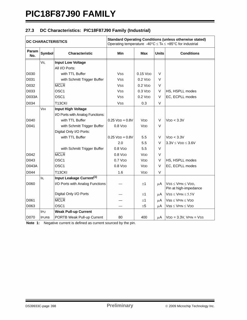
PIC18F87J90 FAMILY
DS39933C-page 398 Preliminary © 2009 Microchip Technology Inc.
27.3 DC Characteristics: PIC18F87J90 Family (Industrial)
DC CHARACTERISTICS Standard Operating Conditions (unless otherwise stated)Operating temperature -40°C ≤ TA ≤ +85°C for industrial
ParamNo. Symbol Characteristic Min Max Units Conditions
VIL Input Low VoltageAll I/O Ports:
D030 with TTL Buffer VSS 0.15 VDD VD031 with Schmitt Trigger Buffer VSS 0.2 VDD V
D032 MCLR VSS 0.2 VDD VD033 OSC1 VSS 0.3 VDD V HS, HSPLL modesD033A
D034
OSC1
T13CKI
VSS
VSS
0.2 VDD
0.3
V
V
EC, ECPLL modes
VIH Input High VoltageI/O Ports with Analog Functions:
D040 with TTL Buffer 0.25 VDD + 0.8V VDD V VDD < 3.3VD041 with Schmitt Trigger Buffer 0.8 VDD VDD V
Digital Only I/O Ports:with TTL Buffer 0.25 VDD + 0.8V 5.5 V VDD < 3.3V
2.0 5.5 V 3.3V ≤ VDD ≤ 3.6V with Schmitt Trigger Buffer 0.8 VDD 5.5 V
D042 MCLR 0.8 VDD VDD VD043 OSC1 0.7 VDD VDD V HS, HSPLL modesD043A
D044
OSC1
T13CKI
0.8 VDD
1.6
VDD
VDD
V
V
EC, ECPLL modes
IIL Input Leakage Current(1) D060 I/O Ports with Analog Functions — ±1 μA VSS ≤ VPIN ≤ VDD,
Pin at high-impedanceDigital Only I/O Ports — ±1 μA VSS ≤ VPIN ≤ 5.5V
D061 MCLR — ±1 μA Vss ≤ VPIN ≤ VDD
D063 OSC1 — ±5 μA Vss ≤ VPIN ≤ VDD IPU Weak Pull-up Current
D070 IPURB PORTB Weak Pull-up Current 80 400 μA VDD = 3.3V, VPIN = VSS
Note 1: Negative current is defined as current sourced by the pin.
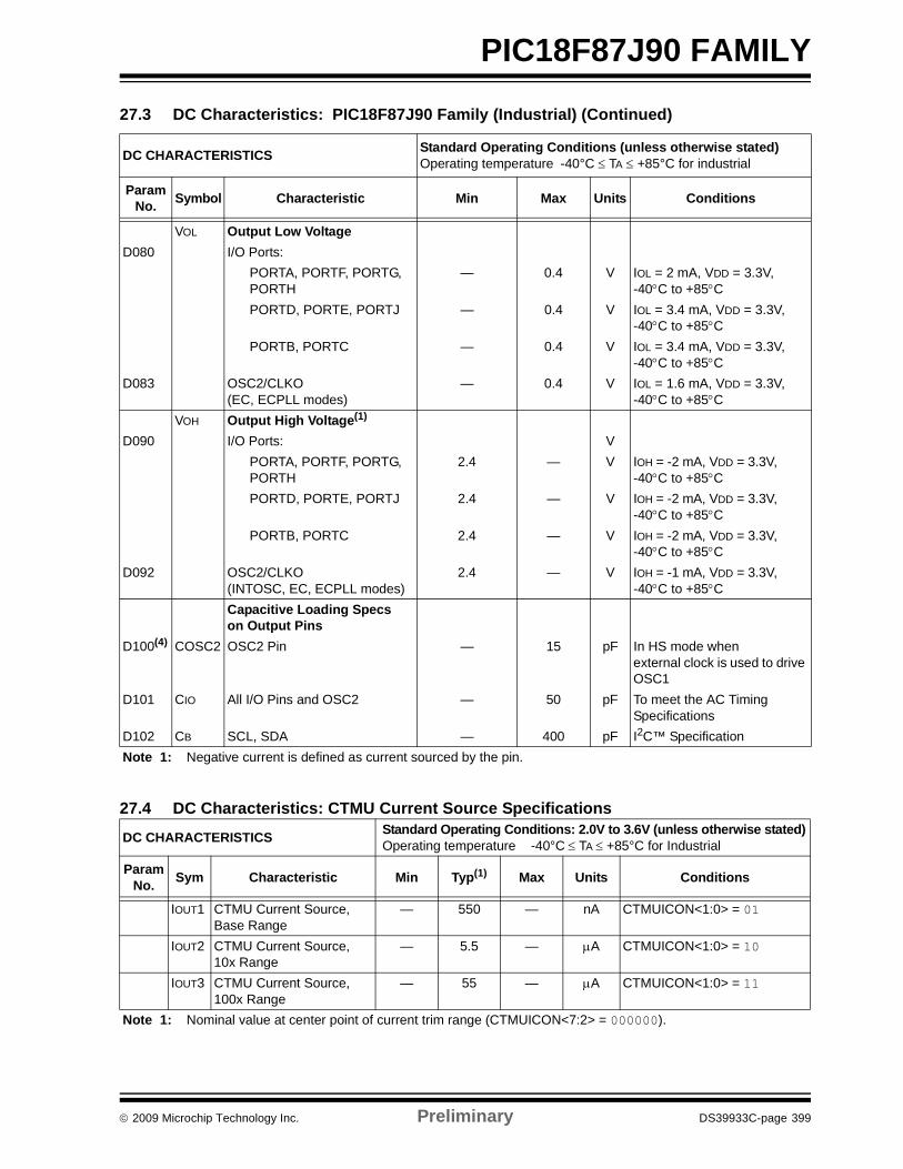
© 2009 Microchip Technology Inc. Preliminary DS39933C-page 399
PIC18F87J90 FAMILY
27.4 DC Characteristics: CTMU Current Source Specifications
VOL Output Low VoltageD080 I/O Ports:
PORTA, PORTF, PORTG,PORTH
— 0.4 V IOL = 2 mA, VDD = 3.3V, -40°C to +85°C
PORTD, PORTE, PORTJ — 0.4 V IOL = 3.4 mA, VDD = 3.3V, -40°C to +85°C
PORTB, PORTC — 0.4 V IOL = 3.4 mA, VDD = 3.3V, -40°C to +85°C
D083 OSC2/CLKO(EC, ECPLL modes)
— 0.4 V IOL = 1.6 mA, VDD = 3.3V, -40°C to +85°C
VOH Output High Voltage(1)
D090 I/O Ports: VPORTA, PORTF, PORTG,PORTH
2.4 — V IOH = -2 mA, VDD = 3.3V,-40°C to +85°C
PORTD, PORTE, PORTJ 2.4 — V IOH = -2 mA, VDD = 3.3V,-40°C to +85°C
PORTB, PORTC 2.4 — V IOH = -2 mA, VDD = 3.3V,-40°C to +85°C
D092 OSC2/CLKO (INTOSC, EC, ECPLL modes)
2.4 — V IOH = -1 mA, VDD = 3.3V,-40°C to +85°C
Capacitive Loading Specson Output Pins
D100(4) COSC2 OSC2 Pin — 15 pF In HS mode when external clock is used to drive OSC1
D101 CIO All I/O Pins and OSC2 — 50 pF To meet the AC Timing Specifications
D102 CB SCL, SDA — 400 pF I2C™ Specification
DC CHARACTERISTICS Standard Operating Conditions: 2.0V to 3.6V (unless otherwise stated)Operating temperature -40°C ≤ TA ≤ +85°C for Industrial
ParamNo. Sym Characteristic Min Typ(1) Max Units Conditions
IOUT1 CTMU Current Source, Base Range
— 550 — nA CTMUICON<1:0> = 01
IOUT2 CTMU Current Source, 10x Range
— 5.5 — μA CTMUICON<1:0> = 10
IOUT3 CTMU Current Source, 100x Range
— 55 — μA CTMUICON<1:0> = 11
Note 1: Nominal value at center point of current trim range (CTMUICON<7:2> = 000000).
27.3 DC Characteristics: PIC18F87J90 Family (Industrial) (Continued)
DC CHARACTERISTICS Standard Operating Conditions (unless otherwise stated)Operating temperature -40°C ≤ TA ≤ +85°C for industrial
ParamNo. Symbol Characteristic Min Max Units Conditions
Note 1: Negative current is defined as current sourced by the pin.
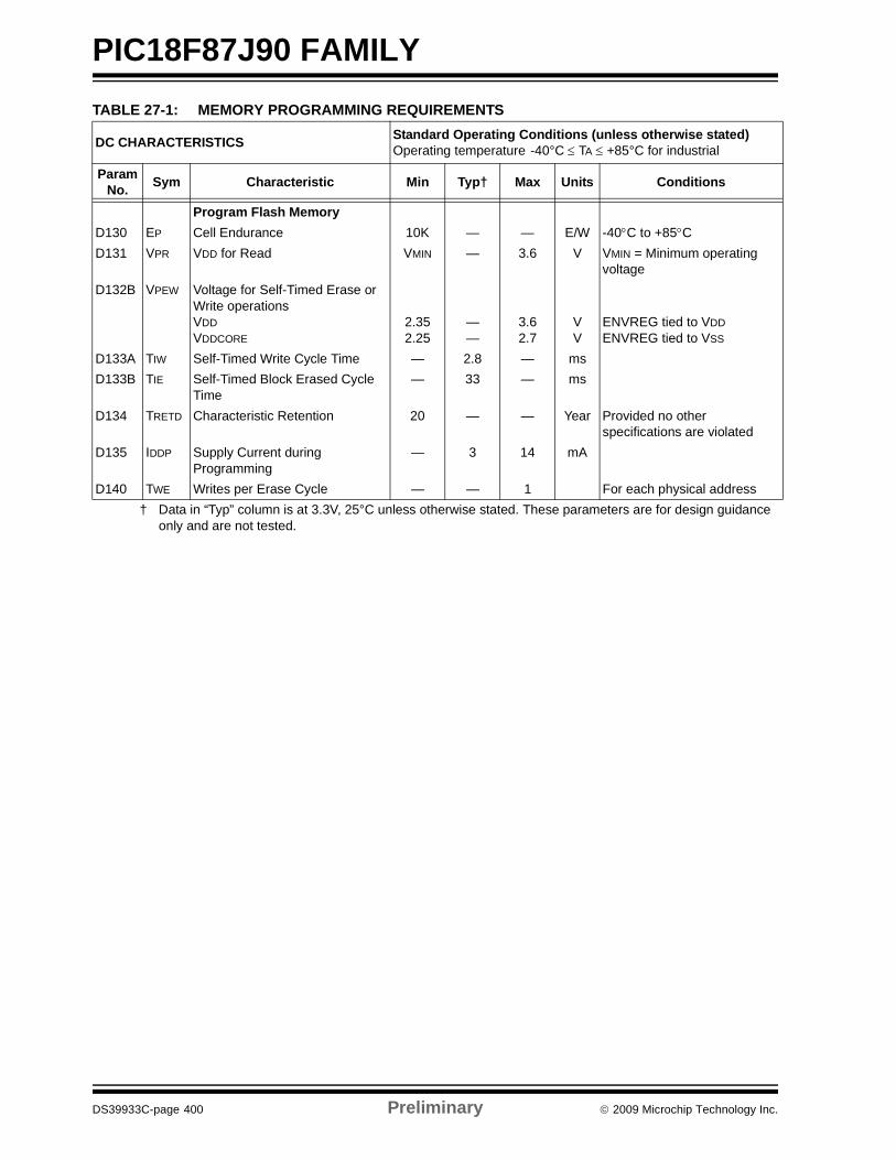
PIC18F87J90 FAMILY
DS39933C-page 400 Preliminary © 2009 Microchip Technology Inc.
TABLE 27-1: MEMORY PROGRAMMING REQUIREMENTS
DC CHARACTERISTICS Standard Operating Conditions (unless otherwise stated)Operating temperature -40°C ≤ TA ≤ +85°C for industrial
ParamNo. Sym Characteristic Min Typ† Max Units Conditions
Program Flash MemoryD130 EP Cell Endurance 10K — — E/W -40°C to +85°CD131 VPR VDD for Read VMIN — 3.6 V VMIN = Minimum operating
voltageD132B VPEW Voltage for Self-Timed Erase or
Write operationsVDDVDDCORE
2.352.25
——
3.62.7
VV
ENVREG tied to VDDENVREG tied to VSS
D133A TIW Self-Timed Write Cycle Time — 2.8 — msD133B TIE Self-Timed Block Erased Cycle
Time— 33 — ms
D134 TRETD Characteristic Retention 20 — — Year Provided no other specifications are violated
D135 IDDP Supply Current during Programming
— 3 14 mA
D140 TWE Writes per Erase Cycle — — 1 For each physical address† Data in “Typ” column is at 3.3V, 25°C unless otherwise stated. These parameters are for design guidance
only and are not tested.
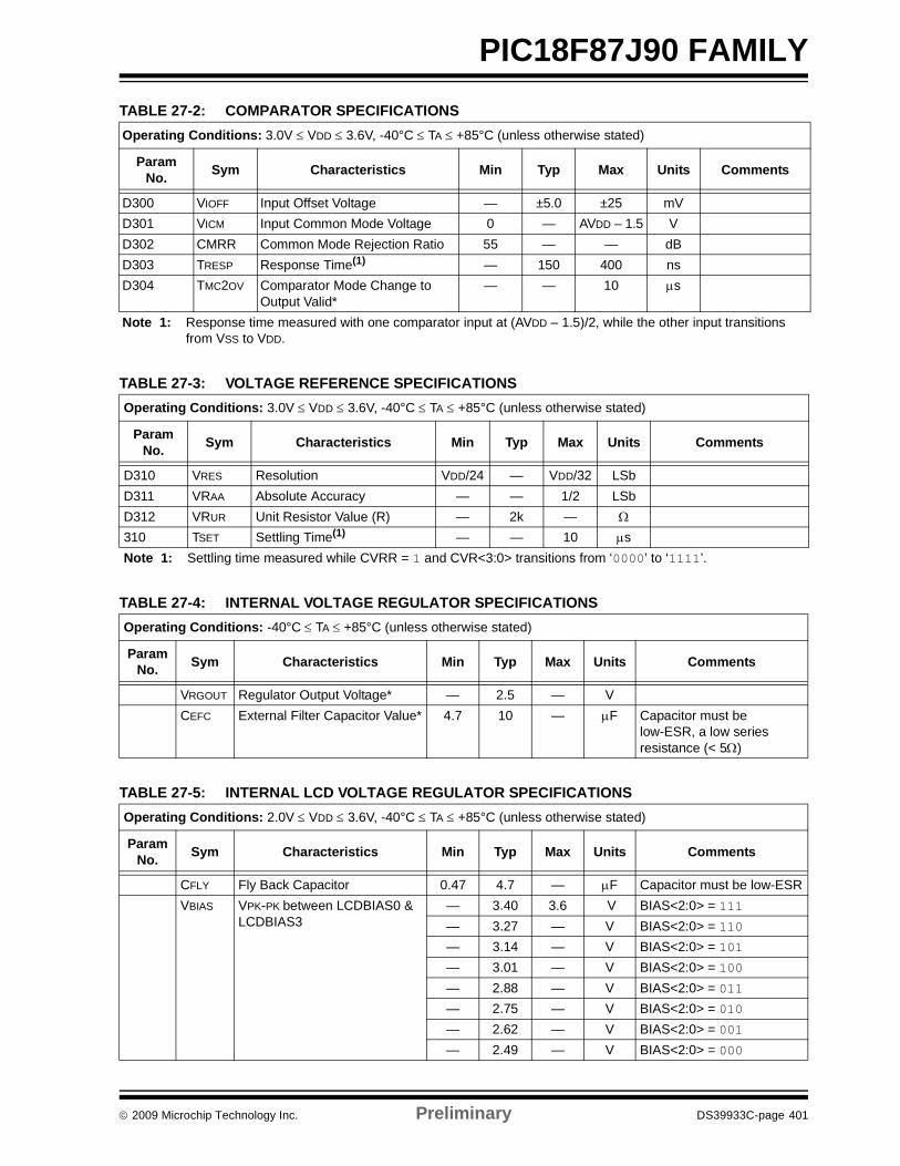
© 2009 Microchip Technology Inc. Preliminary DS39933C-page 401
PIC18F87J90 FAMILYTABLE 27-2: COMPARATOR SPECIFICATIONS
TABLE 27-3: VOLTAGE REFERENCE SPECIFICATIONS
TABLE 27-4: INTERNAL VOLTAGE REGULATOR SPECIFICATIONS
TABLE 27-5: INTERNAL LCD VOLTAGE REGULATOR SPECIFICATIONS
Operating Conditions: 3.0V ≤ VDD ≤ 3.6V, -40°C ≤ TA ≤ +85°C (unless otherwise stated)
ParamNo. Sym Characteristics Min Typ Max Units Comments
D300 VIOFF Input Offset Voltage — ±5.0 ±25 mVD301 VICM Input Common Mode Voltage 0 — AVDD – 1.5 VD302 CMRR Common Mode Rejection Ratio 55 — — dBD303 TRESP Response Time(1) — 150 400 nsD304 TMC2OV Comparator Mode Change to
Output Valid*— — 10 μs
Note 1: Response time measured with one comparator input at (AVDD – 1.5)/2, while the other input transitions from VSS to VDD.
Operating Conditions: 3.0V ≤ VDD ≤ 3.6V, -40°C ≤ TA ≤ +85°C (unless otherwise stated)
ParamNo. Sym Characteristics Min Typ Max Units Comments
D310 VRES Resolution VDD/24 — VDD/32 LSbD311 VRAA Absolute Accuracy — — 1/2 LSbD312 VRUR Unit Resistor Value (R) — 2k — Ω
310 TSET Settling Time(1) — — 10 μsNote 1: Settling time measured while CVRR = 1 and CVR<3:0> transitions from ‘0000’ to ‘1111’.
Operating Conditions: -40°C ≤ TA ≤ +85°C (unless otherwise stated)
ParamNo. Sym Characteristics Min Typ Max Units Comments
VRGOUT Regulator Output Voltage* — 2.5 — VCEFC External Filter Capacitor Value* 4.7 10 — μF Capacitor must be
low-ESR, a low series resistance (< 5Ω)
Operating Conditions: 2.0V ≤ VDD ≤ 3.6V, -40°C ≤ TA ≤ +85°C (unless otherwise stated)
ParamNo. Sym Characteristics Min Typ Max Units Comments
CFLY Fly Back Capacitor 0.47 4.7 — μF Capacitor must be low-ESRVBIAS VPK-PK between LCDBIAS0 &
LCDBIAS3— 3.40 3.6 V BIAS<2:0> = 111— 3.27 — V BIAS<2:0> = 110— 3.14 — V BIAS<2:0> = 101— 3.01 — V BIAS<2:0> = 100— 2.88 — V BIAS<2:0> = 011— 2.75 — V BIAS<2:0> = 010— 2.62 — V BIAS<2:0> = 001— 2.49 — V BIAS<2:0> = 000
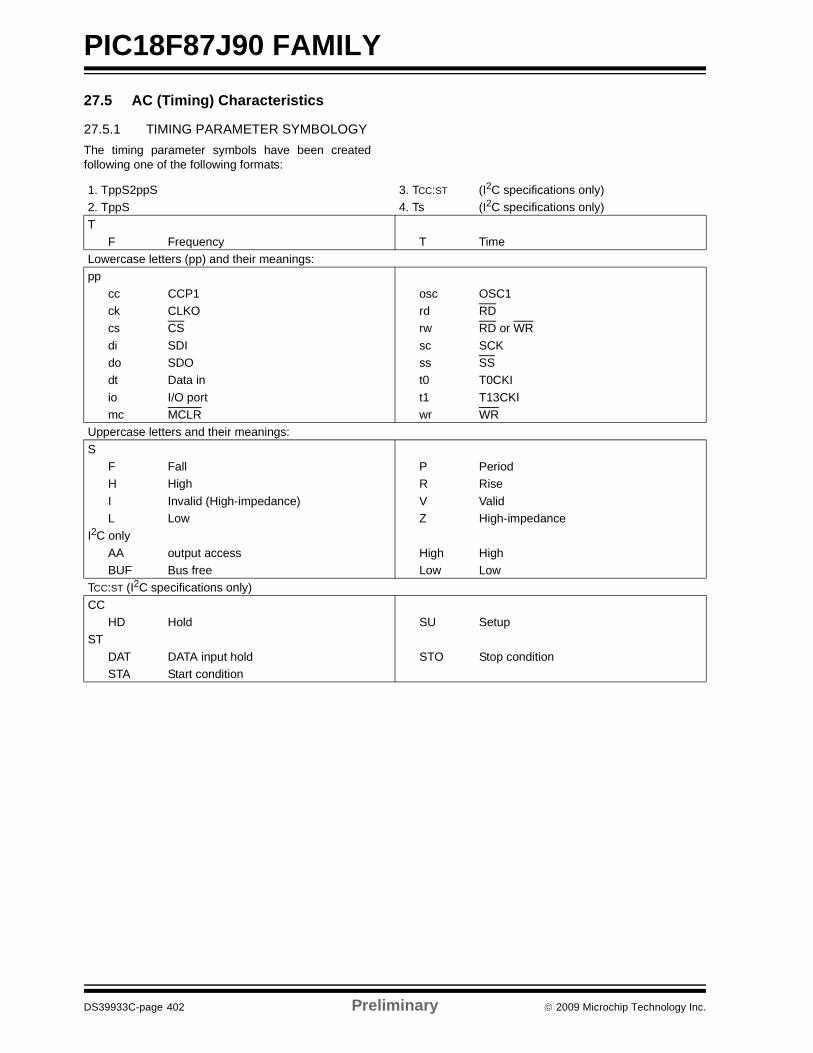
PIC18F87J90 FAMILY
DS39933C-page 402 Preliminary © 2009 Microchip Technology Inc.
27.5 AC (Timing) Characteristics
27.5.1 TIMING PARAMETER SYMBOLOGYThe timing parameter symbols have been createdfollowing one of the following formats:
1. TppS2ppS 3. TCC:ST (I2C specifications only)2. TppS 4. Ts (I2C specifications only)T
F Frequency T TimeLowercase letters (pp) and their meanings:pp
cc CCP1 osc OSC1ck CLKO rd RDcs CS rw RD or WRdi SDI sc SCKdo SDO ss SSdt Data in t0 T0CKIio I/O port t1 T13CKImc MCLR wr WR
Uppercase letters and their meanings:S
F Fall P PeriodH High R RiseI Invalid (High-impedance) V ValidL Low Z High-impedance
I2C onlyAA output access High HighBUF Bus free Low Low
TCC:ST (I2C specifications only)CC
HD Hold SU SetupST
DAT DATA input hold STO Stop conditionSTA Start condition
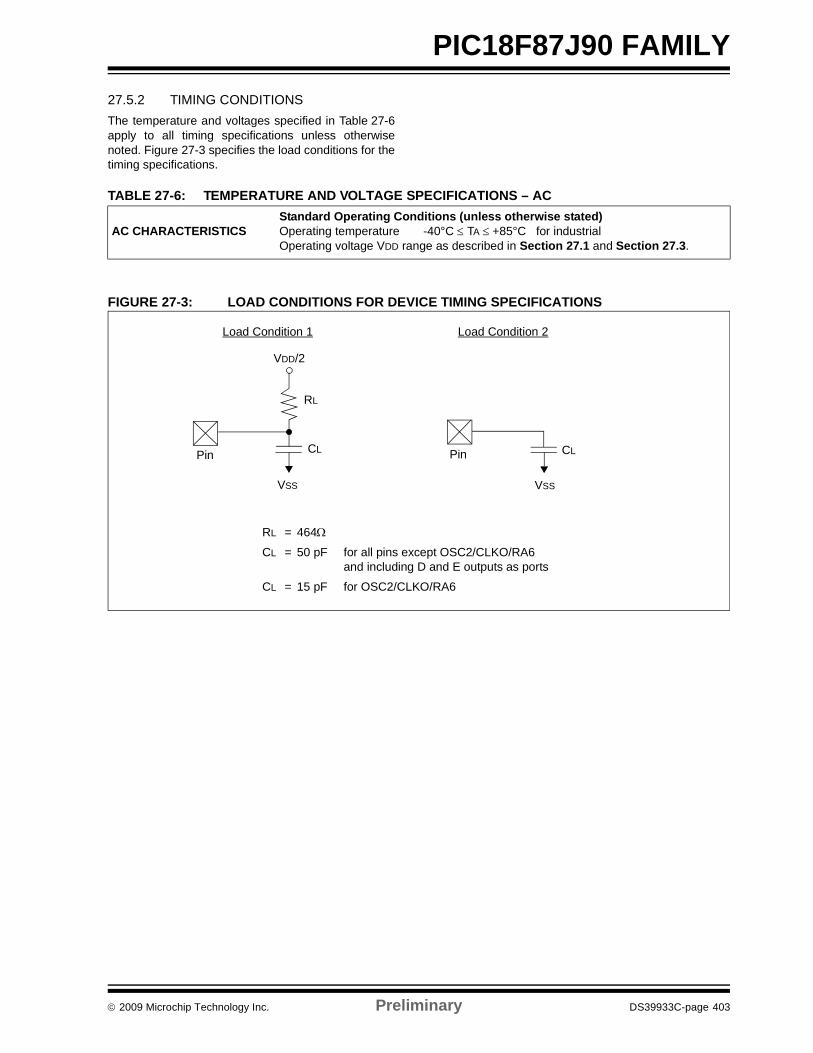
© 2009 Microchip Technology Inc. Preliminary DS39933C-page 403
PIC18F87J90 FAMILY27.5.2 TIMING CONDITIONSThe temperature and voltages specified in Table 27-6apply to all timing specifications unless otherwisenoted. Figure 27-3 specifies the load conditions for thetiming specifications.
TABLE 27-6: TEMPERATURE AND VOLTAGE SPECIFICATIONS – AC
FIGURE 27-3: LOAD CONDITIONS FOR DEVICE TIMING SPECIFICATIONS
AC CHARACTERISTICSStandard Operating Conditions (unless otherwise stated)Operating temperature -40°C ≤ TA ≤ +85°C for industrialOperating voltage VDD range as described in Section 27.1 and Section 27.3.
VDD/2
CL
RL
Pin Pin
VSS VSS
CL
RL = 464Ω
CL = 50 pF for all pins except OSC2/CLKO/RA6 and including D and E outputs as ports
CL = 15 pF for OSC2/CLKO/RA6
Load Condition 1 Load Condition 2
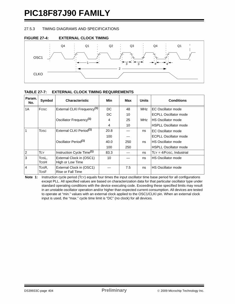
PIC18F87J90 FAMILY
DS39933C-page 404 Preliminary © 2009 Microchip Technology Inc.
27.5.3 TIMING DIAGRAMS AND SPECIFICATIONS
FIGURE 27-4: EXTERNAL CLOCK TIMING
TABLE 27-7: EXTERNAL CLOCK TIMING REQUIREMENTS Param.
No. Symbol Characteristic Min Max Units Conditions
1A FOSC External CLKI Frequency(1) DC 48 MHz EC Oscillator modeDC 10 ECPLL Oscillator mode
Oscillator Frequency(1) 4 25 MHz HS Oscillator mode4 10 HSPLL Oscillator mode
1 TOSC External CLKI Period(1) 20.8 — ns EC Oscillator mode100 — ECPLL Oscillator mode
Oscillator Period(1) 40.0 250 ns HS Oscillator mode100 250 HSPLL Oscillator mode
2 TCY Instruction Cycle Time(1) 83.3 — ns TCY = 4/FOSC, Industrial3 TOSL,
TOSHExternal Clock in (OSC1) High or Low Time
10 — ns HS Oscillator mode
4 TOSR,TOSF
External Clock in (OSC1) Rise or Fall Time
— 7.5 ns HS Oscillator mode
Note 1: Instruction cycle period (TCY) equals four times the input oscillator time base period for all configurations except PLL. All specified values are based on characterization data for that particular oscillator type under standard operating conditions with the device executing code. Exceeding these specified limits may result in an unstable oscillator operation and/or higher than expected current consumption. All devices are tested to operate at “min.” values with an external clock applied to the OSC1/CLKI pin. When an external clock input is used, the “max.” cycle time limit is “DC” (no clock) for all devices.
OSC1
CLKO
Q4 Q1 Q2 Q3 Q4 Q1
1
23 3 4 4
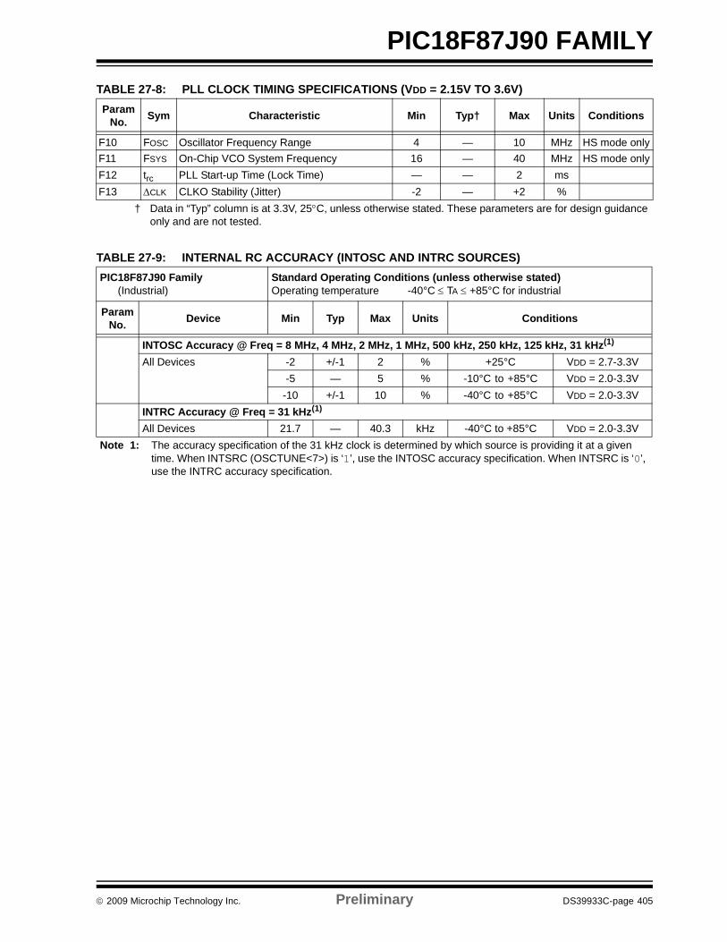
© 2009 Microchip Technology Inc. Preliminary DS39933C-page 405
PIC18F87J90 FAMILYTABLE 27-8: PLL CLOCK TIMING SPECIFICATIONS (VDD = 2.15V TO 3.6V)
TABLE 27-9: INTERNAL RC ACCURACY (INTOSC AND INTRC SOURCES)
Param No. Sym Characteristic Min Typ† Max Units Conditions
F10 FOSC Oscillator Frequency Range 4 — 10 MHz HS mode onlyF11 FSYS On-Chip VCO System Frequency 16 — 40 MHz HS mode onlyF12 trc PLL Start-up Time (Lock Time) — — 2 msF13 ΔCLK CLKO Stability (Jitter) -2 — +2 %
† Data in “Typ” column is at 3.3V, 25°C, unless otherwise stated. These parameters are for design guidance only and are not tested.
PIC18F87J90 Family (Industrial)
Standard Operating Conditions (unless otherwise stated)Operating temperature -40°C ≤ TA ≤ +85°C for industrial
ParamNo. Device Min Typ Max Units Conditions
INTOSC Accuracy @ Freq = 8 MHz, 4 MHz, 2 MHz, 1 MHz, 500 kHz, 250 kHz, 125 kHz, 31 kHz(1)
All Devices -2 +/-1 2 % +25°C VDD = 2.7-3.3V-5 — 5 % -10°C to +85°C VDD = 2.0-3.3V
-10 +/-1 10 % -40°C to +85°C VDD = 2.0-3.3VINTRC Accuracy @ Freq = 31 kHz(1)
All Devices 21.7 — 40.3 kHz -40°C to +85°C VDD = 2.0-3.3VNote 1: The accuracy specification of the 31 kHz clock is determined by which source is providing it at a given
time. When INTSRC (OSCTUNE<7>) is ‘1’, use the INTOSC accuracy specification. When INTSRC is ‘0’, use the INTRC accuracy specification.
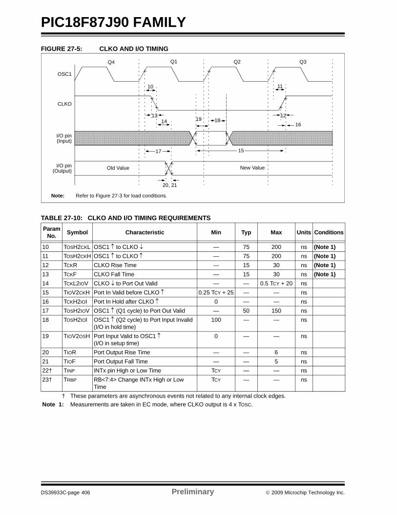
PIC18F87J90 FAMILY
DS39933C-page 406 Preliminary © 2009 Microchip Technology Inc.
FIGURE 27-5: CLKO AND I/O TIMING
TABLE 27-10: CLKO AND I/O TIMING REQUIREMENTS Param
No. Symbol Characteristic Min Typ Max Units Conditions
10 TOSH2CKL OSC1 ↑ to CLKO ↓ — 75 200 ns (Note 1)11 TOSH2CKH OSC1 ↑ to CLKO ↑ — 75 200 ns (Note 1)12 TCKR CLKO Rise Time — 15 30 ns (Note 1)13 TCKF CLKO Fall Time — 15 30 ns (Note 1)14 TCKL2IOV CLKO ↓ to Port Out Valid — — 0.5 TCY + 20 ns15 TIOV2CKH Port In Valid before CLKO ↑ 0.25 TCY + 25 — — ns 16 TCKH2IOI Port In Hold after CLKO ↑ 0 — — ns17 TOSH2IOV OSC1 ↑ (Q1 cycle) to Port Out Valid — 50 150 ns18 TOSH2IOI OSC1 ↑ (Q2 cycle) to Port Input Invalid
(I/O in hold time)100 — — ns
19 TIOV2OSH Port Input Valid to OSC1 ↑ (I/O in setup time)
0 — — ns
20 TIOR Port Output Rise Time — — 6 ns21 TIOF Port Output Fall Time — — 5 ns22† TINP INTx pin High or Low Time TCY — — ns23† TRBP RB<7:4> Change INTx High or Low
TimeTCY — — ns
† These parameters are asynchronous events not related to any internal clock edges.Note 1: Measurements are taken in EC mode, where CLKO output is 4 x TOSC.
Note: Refer to Figure 27-3 for load conditions.
OSC1
CLKO
I/O pin(Input)
I/O pin(Output)
Q4 Q1 Q2 Q3
10
1314
17
20, 21
19 18
15
11
12
16
Old Value New Value
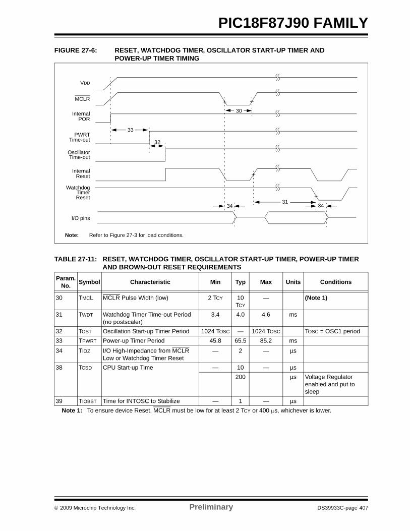
© 2009 Microchip Technology Inc. Preliminary DS39933C-page 407
PIC18F87J90 FAMILYFIGURE 27-6: RESET, WATCHDOG TIMER, OSCILLATOR START-UP TIMER AND
POWER-UP TIMER TIMING
TABLE 27-11: RESET, WATCHDOG TIMER, OSCILLATOR START-UP TIMER, POWER-UP TIMER AND BROWN-OUT RESET REQUIREMENTS
Param. No. Symbol Characteristic Min Typ Max Units Conditions
30 TMCL MCLR Pulse Width (low) 2 TCY 10 TCY
— (Note 1)
31 TWDT Watchdog Timer Time-out Period (no postscaler)
3.4 4.0 4.6 ms
32 TOST Oscillation Start-up Timer Period 1024 TOSC — 1024 TOSC TOSC = OSC1 period33 TPWRT Power-up Timer Period 45.8 65.5 85.2 ms
34 TIOZ I/O High-Impedance from MCLR Low or Watchdog Timer Reset
— 2 — µs
38 TCSD CPU Start-up Time — 10 — µs200 µs Voltage Regulator
enabled and put to sleep
39 TIOBST Time for INTOSC to Stabilize — 1 — µsNote 1: To ensure device Reset, MCLR must be low for at least 2 TCY or 400 μs, whichever is lower.
VDD
MCLR
InternalPOR
PWRTTime-out
OscillatorTime-out
InternalReset
WatchdogTimerReset
33
32
30
3134
I/O pins
34
Note: Refer to Figure 27-3 for load conditions.
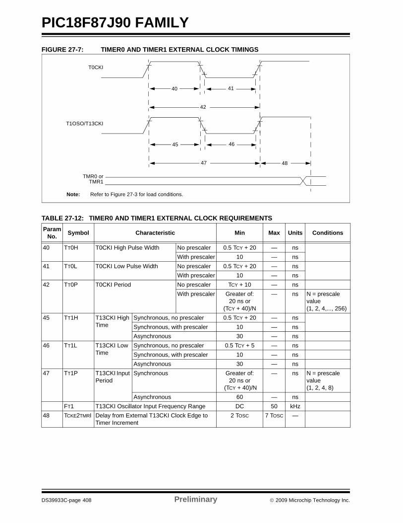
PIC18F87J90 FAMILY
DS39933C-page 408 Preliminary © 2009 Microchip Technology Inc.
FIGURE 27-7: TIMER0 AND TIMER1 EXTERNAL CLOCK TIMINGS
TABLE 27-12: TIMER0 AND TIMER1 EXTERNAL CLOCK REQUIREMENTS Param
No. Symbol Characteristic Min Max Units Conditions
40 TT0H T0CKI High Pulse Width No prescaler 0.5 TCY + 20 — nsWith prescaler 10 — ns
41 TT0L T0CKI Low Pulse Width No prescaler 0.5 TCY + 20 — nsWith prescaler 10 — ns
42 TT0P T0CKI Period No prescaler TCY + 10 — nsWith prescaler Greater of:
20 ns or (TCY + 40)/N
— ns N = prescalevalue (1, 2, 4,..., 256)
45 TT1H T13CKI High Time
Synchronous, no prescaler 0.5 TCY + 20 — nsSynchronous, with prescaler 10 — nsAsynchronous 30 — ns
46 TT1L T13CKI Low Time
Synchronous, no prescaler 0.5 TCY + 5 — nsSynchronous, with prescaler 10 — nsAsynchronous 30 — ns
47 TT1P T13CKI Input Period
Synchronous Greater of:20 ns or
(TCY + 40)/N
— ns N = prescalevalue (1, 2, 4, 8)
Asynchronous 60 — nsFT1 T13CKI Oscillator Input Frequency Range DC 50 kHz
48 TCKE2TMRI Delay from External T13CKI Clock Edge to Timer Increment
2 TOSC 7 TOSC —
Note: Refer to Figure 27-3 for load conditions.
46
47
45
48
41
42
40
T0CKI
T1OSO/T13CKI
TMR0 orTMR1
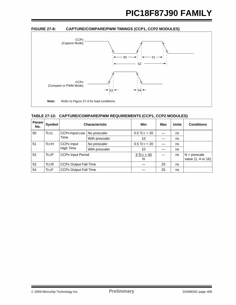
© 2009 Microchip Technology Inc. Preliminary DS39933C-page 409
PIC18F87J90 FAMILYFIGURE 27-8: CAPTURE/COMPARE/PWM TIMINGS (CCP1, CCP2 MODULES)
TABLE 27-13: CAPTURE/COMPARE/PWM REQUIREMENTS (CCP1, CCP2 MODULES) Param
No. Symbol Characteristic Min Max Units Conditions
50 TCCL CCPx Input Low Time
No prescaler 0.5 TCY + 20 — nsWith prescaler 10 — ns
51 TCCH CCPx Input High Time
No prescaler 0.5 TCY + 20 — nsWith prescaler 10 — ns
52 TCCP CCPx Input Period 3 TCY + 40N
— ns N = prescale value (1, 4 or 16)
53 TCCR CCPx Output Fall Time — 25 ns54 TCCF CCPx Output Fall Time — 25 ns
Note: Refer to Figure 27-3 for load conditions.
CCPx(Capture Mode)
50 51
52
CCPx
53 54(Compare or PWM Mode)
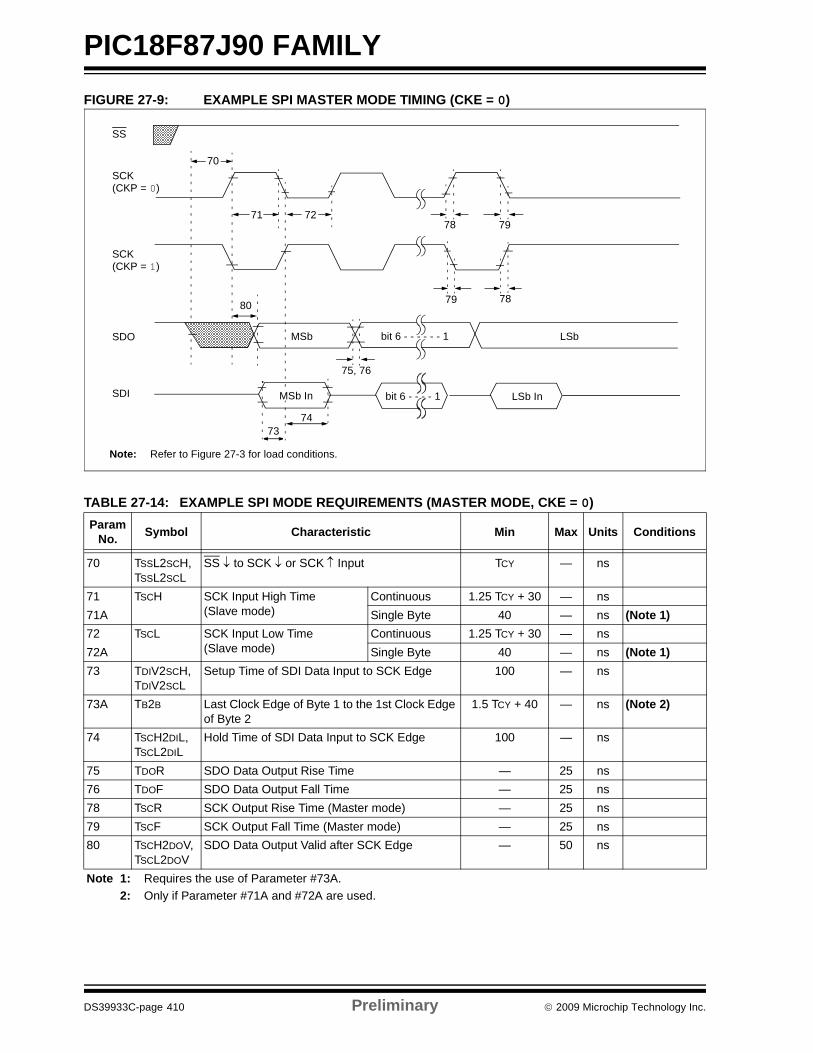
PIC18F87J90 FAMILY
DS39933C-page 410 Preliminary © 2009 Microchip Technology Inc.
FIGURE 27-9: EXAMPLE SPI MASTER MODE TIMING (CKE = 0)
TABLE 27-14: EXAMPLE SPI MODE REQUIREMENTS (MASTER MODE, CKE = 0) Param
No. Symbol Characteristic Min Max Units Conditions
70 TSSL2SCH, TSSL2SCL
SS ↓ to SCK ↓ or SCK ↑ Input TCY — ns
71 TSCH SCK Input High Time (Slave mode)
Continuous 1.25 TCY + 30 — ns71A Single Byte 40 — ns (Note 1)72 TSCL SCK Input Low Time
(Slave mode)Continuous 1.25 TCY + 30 — ns
72A Single Byte 40 — ns (Note 1)73 TDIV2SCH,
TDIV2SCLSetup Time of SDI Data Input to SCK Edge 100 — ns
73A TB2B Last Clock Edge of Byte 1 to the 1st Clock Edge of Byte 2
1.5 TCY + 40 — ns (Note 2)
74 TSCH2DIL, TSCL2DIL
Hold Time of SDI Data Input to SCK Edge 100 — ns
75 TDOR SDO Data Output Rise Time — 25 ns76 TDOF SDO Data Output Fall Time — 25 ns78 TSCR SCK Output Rise Time (Master mode) — 25 ns79 TSCF SCK Output Fall Time (Master mode) — 25 ns80 TSCH2DOV,
TSCL2DOVSDO Data Output Valid after SCK Edge — 50 ns
Note 1: Requires the use of Parameter #73A.2: Only if Parameter #71A and #72A are used.
SS
SCK(CKP = 0)
SCK(CKP = 1)
SDO
SDI
70
71 72
7374
75, 76
787980
7978
MSb LSbbit 6 - - - - - - 1
LSb Inbit 6 - - - - 1
Note: Refer to Figure 27-3 for load conditions.
MSb In
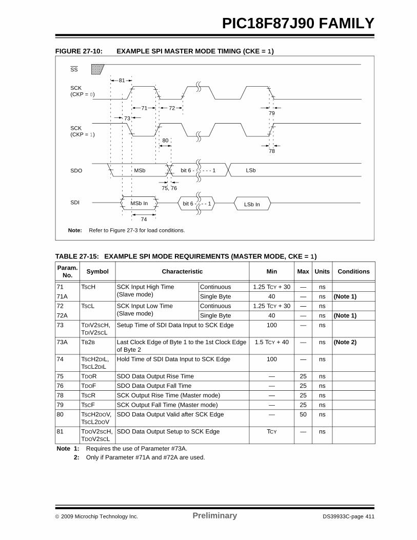
© 2009 Microchip Technology Inc. Preliminary DS39933C-page 411
PIC18F87J90 FAMILYFIGURE 27-10: EXAMPLE SPI MASTER MODE TIMING (CKE = 1)
TABLE 27-15: EXAMPLE SPI MODE REQUIREMENTS (MASTER MODE, CKE = 1) Param.
No. Symbol Characteristic Min Max Units Conditions
71 TSCH SCK Input High Time (Slave mode)
Continuous 1.25 TCY + 30 — ns71A Single Byte 40 — ns (Note 1)72 TSCL SCK Input Low Time
(Slave mode)Continuous 1.25 TCY + 30 — ns
72A Single Byte 40 — ns (Note 1)73 TDIV2SCH,
TDIV2SCLSetup Time of SDI Data Input to SCK Edge 100 — ns
73A TB2B Last Clock Edge of Byte 1 to the 1st Clock Edge of Byte 2
1.5 TCY + 40 — ns (Note 2)
74 TSCH2DIL, TSCL2DIL
Hold Time of SDI Data Input to SCK Edge 100 — ns
75 TDOR SDO Data Output Rise Time — 25 ns76 TDOF SDO Data Output Fall Time — 25 ns78 TSCR SCK Output Rise Time (Master mode) — 25 ns79 TSCF SCK Output Fall Time (Master mode) — 25 ns80 TSCH2DOV,
TSCL2DOVSDO Data Output Valid after SCK Edge — 50 ns
81 TDOV2SCH,TDOV2SCL
SDO Data Output Setup to SCK Edge TCY — ns
Note 1: Requires the use of Parameter #73A.2: Only if Parameter #71A and #72A are used.
SS
SCK(CKP = 0)
SCK(CKP = 1)
SDO
SDI
81
71 72
74
75, 76
78
80
MSb
7973
bit 6 - - - - - - 1
LSb Inbit 6 - - - - 1
LSb
Note: Refer to Figure 27-3 for load conditions.
MSb In
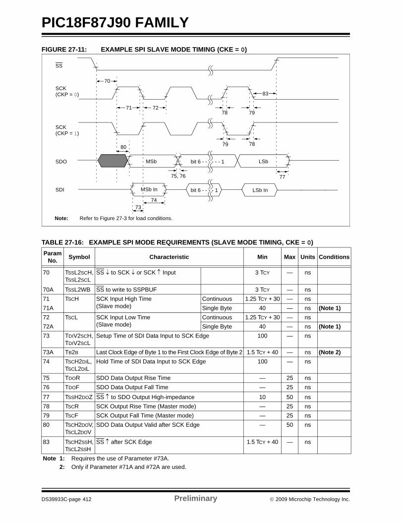
PIC18F87J90 FAMILY
DS39933C-page 412 Preliminary © 2009 Microchip Technology Inc.
FIGURE 27-11: EXAMPLE SPI SLAVE MODE TIMING (CKE = 0)
TABLE 27-16: EXAMPLE SPI MODE REQUIREMENTS (SLAVE MODE TIMING, CKE = 0) Param
No. Symbol Characteristic Min Max Units Conditions
70 TSSL2SCH, TSSL2SCL
SS ↓ to SCK ↓ or SCK ↑ Input 3 TCY — ns
70A TSSL2WB SS to write to SSPBUF 3 TCY — ns71 TSCH SCK Input High Time
(Slave mode)Continuous 1.25 TCY + 30 — ns
71A Single Byte 40 — ns (Note 1)72 TSCL SCK Input Low Time
(Slave mode)Continuous 1.25 TCY + 30 — ns
72A Single Byte 40 — ns (Note 1)73 TDIV2SCH,
TDIV2SCLSetup Time of SDI Data Input to SCK Edge 100 — ns
73A TB2B Last Clock Edge of Byte 1 to the First Clock Edge of Byte 2 1.5 TCY + 40 — ns (Note 2)74 TSCH2DIL,
TSCL2DILHold Time of SDI Data Input to SCK Edge 100 — ns
75 TDOR SDO Data Output Rise Time — 25 ns76 TDOF SDO Data Output Fall Time — 25 ns
77 TSSH2DOZ SS ↑ to SDO Output High-impedance 10 50 ns78 TSCR SCK Output Rise Time (Master mode) — 25 ns79 TSCF SCK Output Fall Time (Master mode) — 25 ns80 TSCH2DOV,
TSCL2DOVSDO Data Output Valid after SCK Edge — 50 ns
83 TSCH2SSH,TSCL2SSH
SS ↑ after SCK Edge 1.5 TCY + 40 — ns
Note 1: Requires the use of Parameter #73A.2: Only if Parameter #71A and #72A are used.
SS
SCK(CKP = 0)
SCK(CKP = 1)
SDO
SDI
70
71 72
7374
75, 76 77
787980
7978
MSb LSbbit 6 - - - - - - 1
bit 6 - - - - 1 LSb In
83
Note: Refer to Figure 27-3 for load conditions.
MSb In
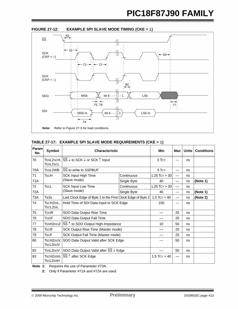
© 2009 Microchip Technology Inc. Preliminary DS39933C-page 413
PIC18F87J90 FAMILYFIGURE 27-12: EXAMPLE SPI SLAVE MODE TIMING (CKE = 1)
TABLE 27-17: EXAMPLE SPI SLAVE MODE REQUIREMENTS (CKE = 1) Param
No. Symbol Characteristic Min Max Units Conditions
70 TSSL2SCH, TSSL2SCL
SS ↓ to SCK ↓ or SCK ↑ Input 3 TCY — ns
70A TSSL2WB SS to write to SSPBUF 3 TCY — ns71 TSCH SCK Input High Time
(Slave mode)Continuous 1.25 TCY + 30 — ns
71A Single Byte 40 — ns (Note 1)72 TSCL SCK Input Low Time
(Slave mode)Continuous 1.25 TCY + 30 — ns
72A Single Byte 40 — ns (Note 1)73A TB2B Last Clock Edge of Byte 1 to the First Clock Edge of Byte 2 1.5 TCY + 40 — ns (Note 2)74 TSCH2DIL,
TSCL2DILHold Time of SDI Data Input to SCK Edge 100 — ns
75 TDOR SDO Data Output Rise Time — 25 ns76 TDOF SDO Data Output Fall Time — 25 ns
77 TSSH2DOZ SS ↑ to SDO Output High-Impedance 10 50 ns78 TSCR SCK Output Rise Time (Master mode) — 25 ns79 TSCF SCK Output Fall Time (Master mode) — 25 ns80 TSCH2DOV,
TSCL2DOVSDO Data Output Valid after SCK Edge — 50 ns
82 TSSL2DOV SDO Data Output Valid after SS ↓ Edge — 50 ns
83 TSCH2SSH,TSCL2SSH
SS ↑ after SCK Edge 1.5 TCY + 40 — ns
Note 1: Requires the use of Parameter #73A.2: Only if Parameter #71A and #72A are used.
SS
SCK(CKP = 0)
SCK(CKP = 1)
SDO
SDI
70
71 72
82
74
75, 76
MSb bit 6 - - - - - - 1 LSb
77
bit 6 - - - - 1 LSb In
80
83
Note: Refer to Figure 27-3 for load conditions.
MSb In
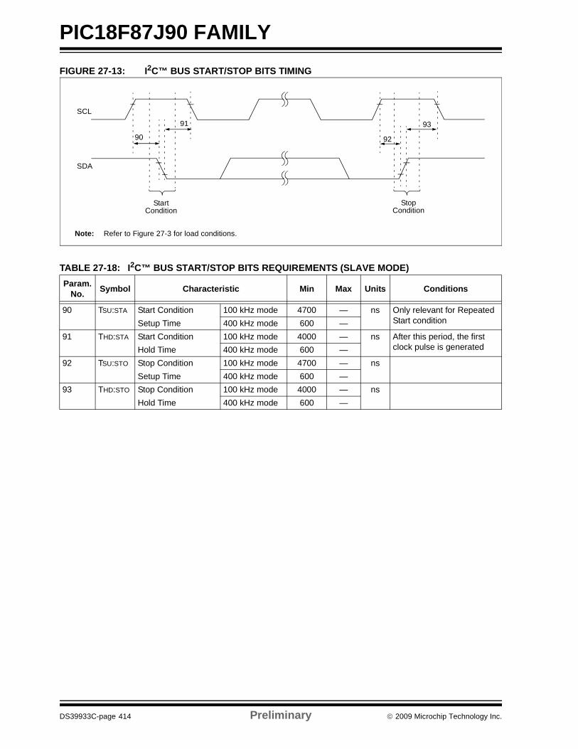
PIC18F87J90 FAMILY
DS39933C-page 414 Preliminary © 2009 Microchip Technology Inc.
FIGURE 27-13: I2C™ BUS START/STOP BITS TIMING
TABLE 27-18: I2C™ BUS START/STOP BITS REQUIREMENTS (SLAVE MODE) Param.
No. Symbol Characteristic Min Max Units Conditions
90 TSU:STA Start Condition 100 kHz mode 4700 — ns Only relevant for Repeated Start conditionSetup Time 400 kHz mode 600 —
91 THD:STA Start Condition 100 kHz mode 4000 — ns After this period, the first clock pulse is generatedHold Time 400 kHz mode 600 —
92 TSU:STO Stop Condition 100 kHz mode 4700 — nsSetup Time 400 kHz mode 600 —
93 THD:STO Stop Condition 100 kHz mode 4000 — nsHold Time 400 kHz mode 600 —
Note: Refer to Figure 27-3 for load conditions.
91
92
93
SCL
SDA
StartCondition
StopCondition
90
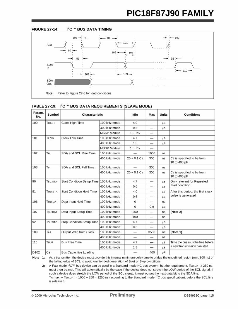
© 2009 Microchip Technology Inc. Preliminary DS39933C-page 415
PIC18F87J90 FAMILYFIGURE 27-14: I2C™ BUS DATA TIMING
TABLE 27-19: I2C™ BUS DATA REQUIREMENTS (SLAVE MODE) Param.
No. Symbol Characteristic Min Max Units Conditions
100 THIGH Clock High Time 100 kHz mode 4.0 — μs400 kHz mode 0.6 — μsMSSP Module 1.5 TCY —
101 TLOW Clock Low Time 100 kHz mode 4.7 — μs400 kHz mode 1.3 — μsMSSP Module 1.5 TCY —
102 TR SDA and SCL Rise Time 100 kHz mode — 1000 ns400 kHz mode 20 + 0.1 CB 300 ns CB is specified to be from
10 to 400 pF 103 TF SDA and SCL Fall Time 100 kHz mode — 300 ns
400 kHz mode 20 + 0.1 CB 300 ns CB is specified to be from 10 to 400 pF
90 TSU:STA Start Condition Setup Time 100 kHz mode 4.7 — μs Only relevant for Repeated Start condition400 kHz mode 0.6 — μs
91 THD:STA Start Condition Hold Time 100 kHz mode 4.0 — μs After this period, the first clock pulse is generated400 kHz mode 0.6 — μs
106 THD:DAT Data Input Hold Time 100 kHz mode 0 — ns400 kHz mode 0 0.9 μs
107 TSU:DAT Data Input Setup Time 100 kHz mode 250 — ns (Note 2)400 kHz mode 100 — ns
92 TSU:STO Stop Condition Setup Time 100 kHz mode 4.7 — μs400 kHz mode 0.6 — μs
109 TAA Output Valid from Clock 100 kHz mode — 3500 ns (Note 1)400 kHz mode — — ns
110 TBUF Bus Free Time 100 kHz mode 4.7 — μs Time the bus must be free before a new transmission can start400 kHz mode 1.3 — μs
D102 CB Bus Capacitive Loading — 400 pF Note 1: As a transmitter, the device must provide this internal minimum delay time to bridge the undefined region (min. 300 ns) of
the falling edge of SCL to avoid unintended generation of Start or Stop conditions.2: A Fast mode I2C™ bus device can be used in a Standard mode I2C bus system, but the requirement, TSU:DAT ≥ 250 ns,
must then be met. This will automatically be the case if the device does not stretch the LOW period of the SCL signal. If such a device does stretch the LOW period of the SCL signal, it must output the next data bit to the SDA line,TR max. + TSU:DAT = 1000 + 250 = 1250 ns (according to the Standard mode I2C bus specification), before the SCL line is released.
Note: Refer to Figure 27-3 for load conditions.
90
91 92
100
101
103
106 107
109 109110
102
SCL
SDAIn
SDAOut
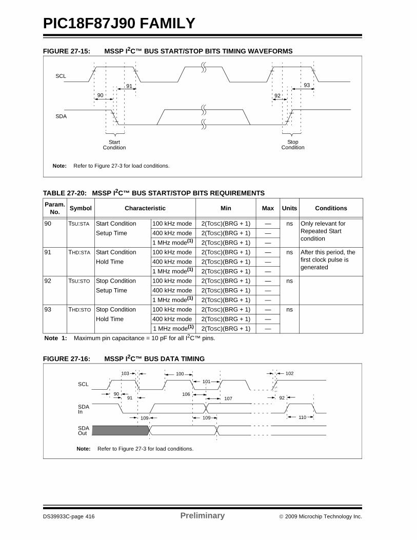
PIC18F87J90 FAMILY
DS39933C-page 416 Preliminary © 2009 Microchip Technology Inc.
FIGURE 27-15: MSSP I2C™ BUS START/STOP BITS TIMING WAVEFORMS
TABLE 27-20: MSSP I2C™ BUS START/STOP BITS REQUIREMENTS
FIGURE 27-16: MSSP I2C™ BUS DATA TIMING
Param.No. Symbol Characteristic Min Max Units Conditions
90 TSU:STA Start Condition 100 kHz mode 2(TOSC)(BRG + 1) — ns Only relevant for Repeated Start condition
Setup Time 400 kHz mode 2(TOSC)(BRG + 1) —1 MHz mode(1) 2(TOSC)(BRG + 1) —
91 THD:STA Start Condition 100 kHz mode 2(TOSC)(BRG + 1) — ns After this period, the first clock pulse is generated
Hold Time 400 kHz mode 2(TOSC)(BRG + 1) —1 MHz mode(1) 2(TOSC)(BRG + 1) —
92 TSU:STO Stop Condition 100 kHz mode 2(TOSC)(BRG + 1) — nsSetup Time 400 kHz mode 2(TOSC)(BRG + 1) —
1 MHz mode(1) 2(TOSC)(BRG + 1) —93 THD:STO Stop Condition 100 kHz mode 2(TOSC)(BRG + 1) — ns
Hold Time 400 kHz mode 2(TOSC)(BRG + 1) —1 MHz mode(1) 2(TOSC)(BRG + 1) —
Note 1: Maximum pin capacitance = 10 pF for all I2C™ pins.
Note: Refer to Figure 27-3 for load conditions.
91 93
SCL
SDA
StartCondition
StopCondition
90 92
Note: Refer to Figure 27-3 for load conditions.
9091 92
100101
103
106107
109 109 110
102
SCL
SDAIn
SDAOut
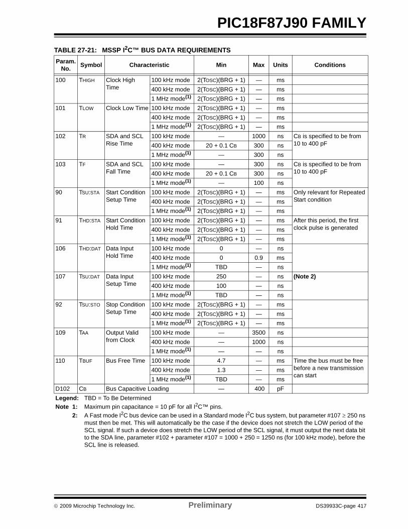
© 2009 Microchip Technology Inc. Preliminary DS39933C-page 417
PIC18F87J90 FAMILYTABLE 27-21: MSSP I2C™ BUS DATA REQUIREMENTS Param.
No. Symbol Characteristic Min Max Units Conditions
100 THIGH Clock High Time
100 kHz mode 2(TOSC)(BRG + 1) — ms400 kHz mode 2(TOSC)(BRG + 1) — ms1 MHz mode(1) 2(TOSC)(BRG + 1) — ms
101 TLOW Clock Low Time 100 kHz mode 2(TOSC)(BRG + 1) — ms400 kHz mode 2(TOSC)(BRG + 1) — ms1 MHz mode(1) 2(TOSC)(BRG + 1) — ms
102 TR SDA and SCL Rise Time
100 kHz mode — 1000 ns CB is specified to be from 10 to 400 pF 400 kHz mode 20 + 0.1 CB 300 ns
1 MHz mode(1) — 300 ns103 TF SDA and SCL
Fall Time100 kHz mode — 300 ns CB is specified to be from
10 to 400 pF 400 kHz mode 20 + 0.1 CB 300 ns1 MHz mode(1) — 100 ns
90 TSU:STA Start Condition Setup Time
100 kHz mode 2(TOSC)(BRG + 1) — ms Only relevant for Repeated Start condition400 kHz mode 2(TOSC)(BRG + 1) — ms
1 MHz mode(1) 2(TOSC)(BRG + 1) — ms91 THD:STA Start Condition
Hold Time 100 kHz mode 2(TOSC)(BRG + 1) — ms After this period, the first
clock pulse is generated400 kHz mode 2(TOSC)(BRG + 1) — ms1 MHz mode(1) 2(TOSC)(BRG + 1) — ms
106 THD:DAT Data Input Hold Time
100 kHz mode 0 — ns400 kHz mode 0 0.9 ms1 MHz mode(1) TBD — ns
107 TSU:DAT Data Input Setup Time
100 kHz mode 250 — ns (Note 2)400 kHz mode 100 — ns1 MHz mode(1) TBD — ns
92 TSU:STO Stop Condition Setup Time
100 kHz mode 2(TOSC)(BRG + 1) — ms400 kHz mode 2(TOSC)(BRG + 1) — ms1 MHz mode(1) 2(TOSC)(BRG + 1) — ms
109 TAA Output Valid from Clock
100 kHz mode — 3500 ns400 kHz mode — 1000 ns1 MHz mode(1) — — ns
110 TBUF Bus Free Time 100 kHz mode 4.7 — ms Time the bus must be free before a new transmission can start
400 kHz mode 1.3 — ms1 MHz mode(1) TBD — ms
D102 CB Bus Capacitive Loading — 400 pF Legend: TBD = To Be DeterminedNote 1: Maximum pin capacitance = 10 pF for all I2C™ pins.
2: A Fast mode I2C bus device can be used in a Standard mode I2C bus system, but parameter #107 ≥ 250 ns must then be met. This will automatically be the case if the device does not stretch the LOW period of the SCL signal. If such a device does stretch the LOW period of the SCL signal, it must output the next data bit to the SDA line, parameter #102 + parameter #107 = 1000 + 250 = 1250 ns (for 100 kHz mode), before the SCL line is released.
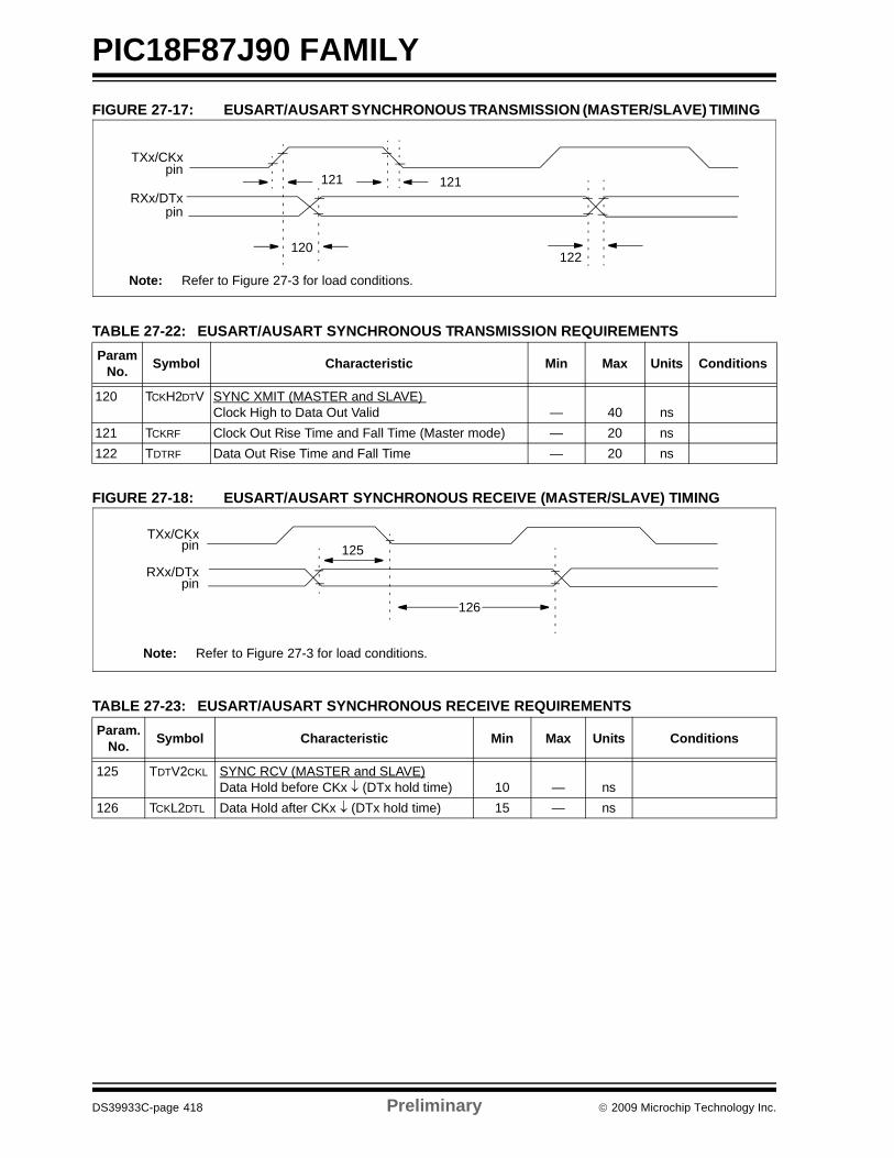
PIC18F87J90 FAMILY
DS39933C-page 418 Preliminary © 2009 Microchip Technology Inc.
FIGURE 27-17: EUSART/AUSART SYNCHRONOUS TRANSMISSION (MASTER/SLAVE) TIMING
TABLE 27-22: EUSART/AUSART SYNCHRONOUS TRANSMISSION REQUIREMENTS
FIGURE 27-18: EUSART/AUSART SYNCHRONOUS RECEIVE (MASTER/SLAVE) TIMING
TABLE 27-23: EUSART/AUSART SYNCHRONOUS RECEIVE REQUIREMENTS
Param No. Symbol Characteristic Min Max Units Conditions
120 TCKH2DTV SYNC XMIT (MASTER and SLAVE) Clock High to Data Out Valid — 40 ns
121 TCKRF Clock Out Rise Time and Fall Time (Master mode) — 20 ns122 TDTRF Data Out Rise Time and Fall Time — 20 ns
Param. No. Symbol Characteristic Min Max Units Conditions
125 TDTV2CKL SYNC RCV (MASTER and SLAVE)Data Hold before CKx ↓ (DTx hold time) 10 — ns
126 TCKL2DTL Data Hold after CKx ↓ (DTx hold time) 15 — ns
121 121
120122
TXx/CKx
RXx/DTxpin
pin
Note: Refer to Figure 27-3 for load conditions.
125
126
TXx/CKx
RXx/DTx
pin
pin
Note: Refer to Figure 27-3 for load conditions.
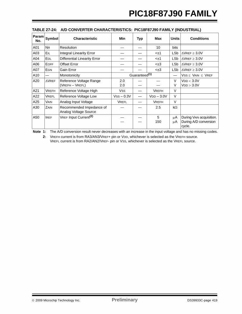
© 2009 Microchip Technology Inc. Preliminary DS39933C-page 419
PIC18F87J90 FAMILYTABLE 27-24: A/D CONVERTER CHARACTERISTICS: PIC18F87J90 FAMILY (INDUSTRIAL)Param
No. Symbol Characteristic Min Typ Max Units Conditions
A01 NR Resolution — — 10 bitsA03 EIL Integral Linearity Error — — <±1 LSb ΔVREF ≥ 3.0V A04 EDL Differential Linearity Error — — <±1 LSb ΔVREF ≥ 3.0V A06 EOFF Offset Error — — <±3 LSb ΔVREF ≥ 3.0V A07 EGN Gain Error — — <±3 LSb ΔVREF ≥ 3.0V A10 — Monotonicity Guaranteed(1) — VSS ≤ VAIN ≤ VREF
A20 ΔVREF Reference Voltage Range(VREFH – VREFL)
2.02.0
——
——
VV
VDD < 3.0VVDD > 3.0V
A21 VREFH Reference Voltage High VSS — VREFH VA22 VREFL Reference Voltage Low VSS – 0.3V — VDD – 3.0V VA25 VAIN Analog Input Voltage VREFL — VREFH VA30 ZAIN Recommended Impedance of
Analog Voltage Source— — 2.5 kΩ
A50 IREF VREF Input Current(2) ——
——
5150
μAμA
During VAIN acquisition.During A/D conversion cycle.
Note 1: The A/D conversion result never decreases with an increase in the input voltage and has no missing codes.2: VREFH current is from RA3/AN3/VREF+ pin or VDD, whichever is selected as the VREFH source.
VREFL current is from RA2/AN2/VREF- pin or VSS, whichever is selected as the VREFL source.
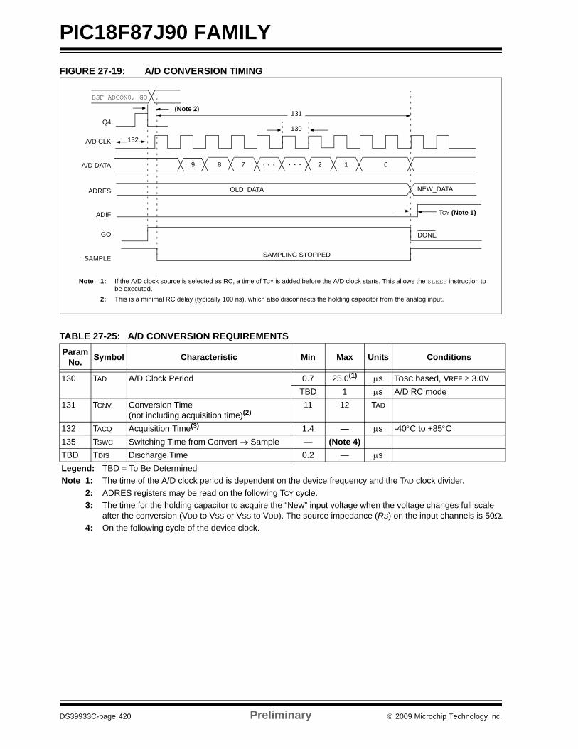
PIC18F87J90 FAMILY
DS39933C-page 420 Preliminary © 2009 Microchip Technology Inc.
FIGURE 27-19: A/D CONVERSION TIMING
TABLE 27-25: A/D CONVERSION REQUIREMENTS Param
No. Symbol Characteristic Min Max Units Conditions
130 TAD A/D Clock Period 0.7 25.0(1) μs TOSC based, VREF ≥ 3.0VTBD 1 μs A/D RC mode
131 TCNV Conversion Time (not including acquisition time)(2)
11 12 TAD
132 TACQ Acquisition Time(3) 1.4 — μs -40°C to +85°C135 TSWC Switching Time from Convert → Sample — (Note 4)TBD TDIS Discharge Time 0.2 — μsLegend: TBD = To Be DeterminedNote 1: The time of the A/D clock period is dependent on the device frequency and the TAD clock divider.
2: ADRES registers may be read on the following TCY cycle.3: The time for the holding capacitor to acquire the “New” input voltage when the voltage changes full scale
after the conversion (VDD to VSS or VSS to VDD). The source impedance (RS) on the input channels is 50Ω.4: On the following cycle of the device clock.
131
130
132
BSF ADCON0, GO
Q4
A/D CLK
A/D DATA
ADRES
ADIF
GO
SAMPLE
OLD_DATA
SAMPLING STOPPED
DONE
NEW_DATA
(Note 2)
9 8 7 2 1 0
Note 1: If the A/D clock source is selected as RC, a time of TCY is added before the A/D clock starts. This allows the SLEEP instruction tobe executed.
2: This is a minimal RC delay (typically 100 ns), which also disconnects the holding capacitor from the analog input.
. . . . . .
TCY (Note 1)
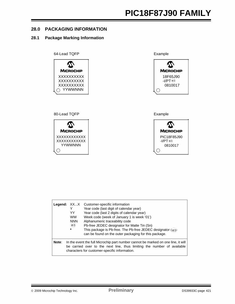
© 2009 Microchip Technology Inc. Preliminary DS39933C-page 421
PIC18F87J90 FAMILY
28.0 PACKAGING INFORMATION
28.1 Package Marking Information
3e
3e
64-Lead TQFP
XXXXXXXXXXXXXXXXXXXXXXXXXXXXXX
YYWWNNN
Example
18F65J90-I/PT0810017
80-Lead TQFP
XXXXXXXXXXXXXXXXXXXXXXXX
YYWWNNN
Example
PIC18F85J90-I/PT
0810017
Legend: XX...X Customer-specific informationY Year code (last digit of calendar year)YY Year code (last 2 digits of calendar year)WW Week code (week of January 1 is week ‘01’)NNN Alphanumeric traceability code Pb-free JEDEC designator for Matte Tin (Sn)* This package is Pb-free. The Pb-free JEDEC designator ( )
can be found on the outer packaging for this package.
Note: In the event the full Microchip part number cannot be marked on one line, it willbe carried over to the next line, thus limiting the number of availablecharacters for customer-specific information.
3e
3e
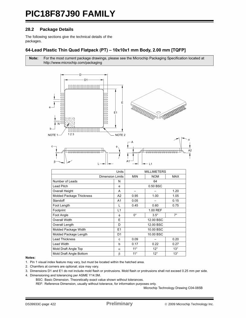
PIC18F87J90 FAMILY
DS39933C-page 422 Preliminary © 2009 Microchip Technology Inc.
28.2 Package Details The following sections give the technical details of thepackages.
!"#$%&
' ( !"# $% &" ' ()"&'"!&) & #*&& & # +'% !& ! &,!- ' ' !!#.#&"# '#%!&"!!#%!&"!!!& $ #/'' !# ' !#& .0/
1+2 1!' ! & $& " !**&"&& !.32 % ' !("!"*&"&& (%%'&"! !
' ( 3& '!&" &4 #*!( ! ! & 4 %&& #&&&255***''54
6&! 77..' !7'&! 8 89 :
8"') %7 #! 8 ;7 #& /1+9 < & = = # #4 4 !! / /&#%% / = /3&7 & 7 / ; /3&& 7 .33& > /> >9 ?#& . 1+9 7 & 1+# #4 ?#& . 1+# #4 7 & 1+7 #4 !! = 7 #?#& ) #%& > > >#%& 1&&' > > >
D
D1
E
E1
e
b
N
NOTE 1 1 2 3 NOTE 2
c
LA1
L1
A2
Aφ
β
α
* +@/1
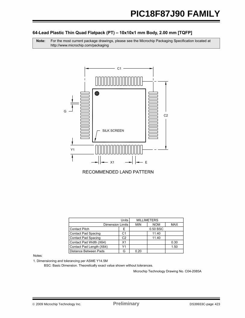
© 2009 Microchip Technology Inc. Preliminary DS39933C-page 423
PIC18F87J90 FAMILY
!"#$%&
' ( 3& '!&" &4 #*!( ! ! & 4 %&& #&&&255***''54
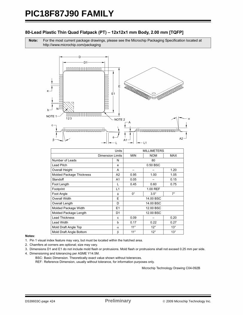
PIC18F87J90 FAMILY
DS39933C-page 424 Preliminary © 2009 Microchip Technology Inc.
) ## !"#$%&
' ( !"# $% &" ' ()"&'"!&) & #*&& & # +'% !& ! &,!- ' ' !!#.#&"# '#%!&"!!#%!&"!!!& $ #/'' !# ' !#& .0/
1+2 1!' ! & $& " !**&"&& !.32 % ' !("!"*&"&& (%%'&"! !
' ( 3& '!&" &4 #*!( ! ! & 4 %&& #&&&255***''54
6&! 77..' !7'&! 8 89 :
8"') %7 #! 8 @7 #& /1+9 < & = = # #4 4 !! / /&#%% / = /3&7 & 7 / ; /3&& 7 .33& > /> >9 ?#& . 1+9 7 & 1+# #4 ?#& . 1+# #4 7 & 1+7 #4 !! = 7 #?#& ) #%& > > >#%& 1&&' > > >
D
D1
E
E1e
b N
NOTE 1123 NOTE 2
A
A2L1
A1L
c
α
βφ
* +1
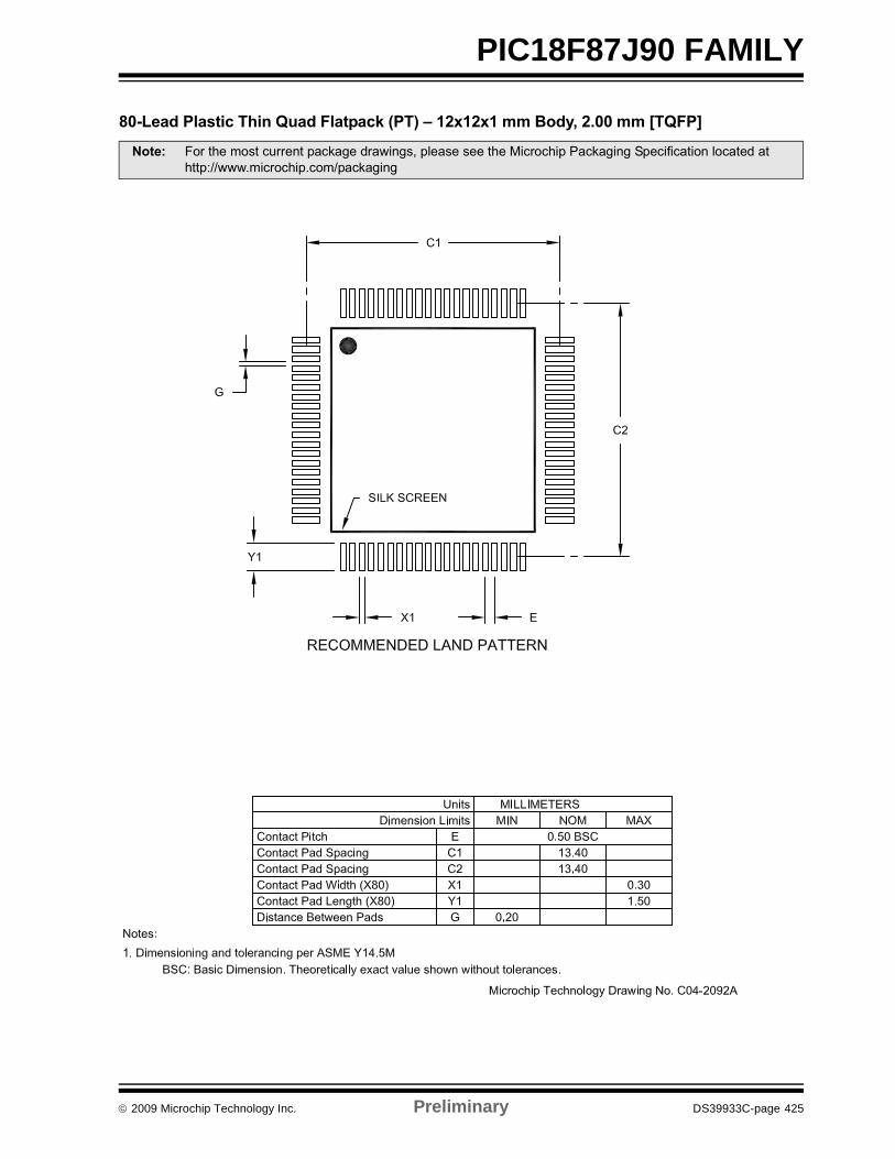
© 2009 Microchip Technology Inc. Preliminary DS39933C-page 425
PIC18F87J90 FAMILY
) ## !"#$%&
' ( 3& '!&" &4 #*!( ! ! & 4 %&& #&&&255***''54

PIC18F87J90 FAMILY
DS39933C-page 426 Preliminary © 2009 Microchip Technology Inc.
NOTES:
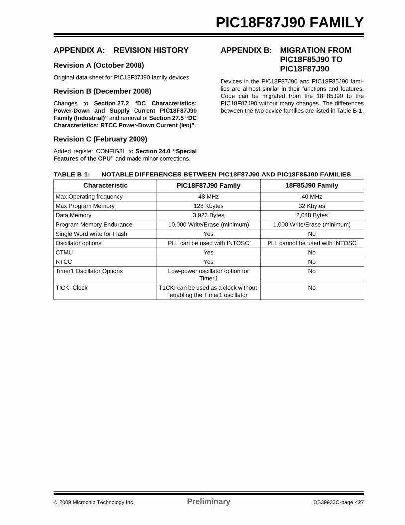
© 2009 Microchip Technology Inc. Preliminary DS39933C-page 427
PIC18F87J90 FAMILY
APPENDIX A: REVISION HISTORY
Revision A (October 2008)Original data sheet for PIC18F87J90 family devices.
Revision B (December 2008)Changes to Section 27.2 “DC Characteristics:Power-Down and Supply Current PIC18F87J90Family (Industrial)” and removal of Section 27.5 “DCCharacteristics: RTCC Power-Down Current (IPD)”.
Revision C (February 2009)Added register CONFIG3L to Section 24.0 “SpecialFeatures of the CPU” and made minor corrections.
APPENDIX B: MIGRATION FROM PIC18F85J90 TO PIC18F87J90
Devices in the PIC18F87J90 and PIC18F85J90 fami-lies are almost similar in their functions and features.Code can be migrated from the 18F85J90 to thePIC18F87J90 without many changes. The differencesbetween the two device families are listed in Table B-1.
TABLE B-1: NOTABLE DIFFERENCES BETWEEN PIC18F87J90 AND PIC18F85J90 FAMILIES Characteristic PIC18F87J90 Family 18F85J90 Family
Max Operating frequency 48 MHz 40 MHzMax Program Memory 128 Kbytes 32 KbytesData Memory 3,923 Bytes 2,048 BytesProgram Memory Endurance 10,000 Write/Erase (minimum) 1,000 Write/Erase (minimum)Single Word write for Flash Yes NoOscillator options PLL can be used with INTOSC PLL cannot be used with INTOSCCTMU Yes NoRTCC Yes NoTimer1 Oscillator Options Low-power oscillator option for
Timer1No
TICKI Clock T1CKI can be used as a clock without enabling the Timer1 oscillator
No

PIC18F87J90 FAMILY
DS39933C-page 428 Preliminary © 2009 Microchip Technology Inc.
NOTES:
© 2009 Microchip Technology Inc. Preliminary DS39933C-page 429
PIC18F87J90 FAMILY
INDEXAA/D .................................................................................... 283
A/D Converter Interrupt, Configuring ........................ 287Acquisition Requirements ......................................... 288ADCAL Bit................................................................. 291ADCON0 Register..................................................... 283ADCON1 Register..................................................... 283ADCON2 Register..................................................... 283ADRESH Register............................................. 283, 286ADRESL Register ..................................................... 283Analog Port Pins, Configuring................................... 289Associated Registers ................................................ 291Automatic Selecting and Configuring
Acquisition Time ............................................... 289Configuring the Module............................................. 287Conversion Clock (TAD) ............................................ 289Conversion Requirements ........................................ 420Conversion Status (GO/DONE Bit) ........................... 286Conversions .............................................................. 290Converter Calibration ................................................ 291Converter Characteristics ......................................... 419Operation in Power-Managed Modes ....................... 291Special Event Trigger (CCP)..................................... 290Use of the CCP2 Trigger........................................... 290
Absolute Maximum Ratings .............................................. 387AC (Timing) Characteristics .............................................. 402
Load Conditions for Device Timing Specifications.... 403Parameter Symbology .............................................. 402Temperature and Voltage Specifications .................. 403Timing Conditions ..................................................... 403
ACKSTAT ......................................................................... 239ACKSTAT Status Flag ...................................................... 239ADCAL Bit ......................................................................... 291ADCON0 Register............................................................. 283
GO/DONE Bit............................................................ 286ADCON1 Register............................................................. 283ADCON2 Register............................................................. 283ADDFSR ........................................................................... 376ADDLW ............................................................................. 339Addressable Universal Synchronous Asynchronous
Receiver Transmitter (AUSART). See AUSART.ADDULNK......................................................................... 376ADDWF............................................................................. 339ADDWFC .......................................................................... 340ADRESH Register............................................................. 283ADRESL Register ..................................................... 283, 286Analog-to-Digital Converter. See A/D.ANDLW ............................................................................. 340ANDWF............................................................................. 341Assembler
MPASM Assembler................................................... 384AUSART
Asynchronous Mode ................................................. 274Associated Registers, Receive ......................... 277Associated Registers, Transmit ........................ 275Receiver............................................................ 276Setting up 9-Bit Mode with Address Detect ...... 276Transmitter........................................................ 274
Baud Rate Generator (BRG)..................................... 272Associated Registers ........................................ 272Baud Rate Error, Calculating ............................ 272Baud Rates, Asynchronous Modes .................. 273High Baud Rate Select (BRGH Bit) .................. 272
Operation in Power-Managed Modes............... 272Sampling .......................................................... 272
Synchronous Master Mode....................................... 278Associated Registers, Receive......................... 280Associated Registers, Transmit........................ 279Reception ......................................................... 280Transmission .................................................... 278
Synchronous Slave Mode......................................... 281Associated Registers, Receive......................... 282Associated Registers, Transmit........................ 281Reception ......................................................... 282Transmission .................................................... 281
BBaud Rate Generator ....................................................... 235BC..................................................................................... 341BCF .................................................................................. 342BF ..................................................................................... 239BF Status Flag.................................................................. 239Bias Generation (LCD)
Charge Pump Design Considerations ...................... 187Block Diagrams
A/D............................................................................ 286Analog Input Model................................................... 287AUSART Receive ..................................................... 276AUSART Transmit .................................................... 274Baud Rate Generator ............................................... 235Capture Mode Operation .......................................... 170Comparator Analog Input Model............................... 297Comparator I/O Operating Modes ............................ 294Comparator Output................................................... 296Comparator Voltage Reference................................ 300Comparator Voltage Reference Output Buffer
Example ........................................................... 301Compare Mode Operation ........................................ 171Connections for On-Chip Voltage Regulator ............ 328CTMU ....................................................................... 303CTMU Current Source Calibration Circuit ................ 306CTMU Typical Connections and Internal
Configuration for Pulse Delay Generation........ 314CTMU Typical Connections and Internal
Configuration for Time Measurement ............... 313Device Clock............................................................... 29EUSART Receive ..................................................... 260EUSART Transmit .................................................... 258External Power-on Reset Circuit (Slow VDD
Power-up) ........................................................... 49Fail-Safe Clock Monitor ............................................ 330Generic I/O Port Operation....................................... 111Interrupt Logic............................................................. 96LCD Clock Generation.............................................. 182LCD Driver Module ................................................... 177LCD Regulator Connections (M0 and M1) ............... 184MSSP (I2C Master Mode)......................................... 233MSSP (I2C Mode)..................................................... 214MSSP (SPI Mode) .................................................... 205On-Chip Reset Circuit................................................. 47PIC18F6XJ90 ............................................................. 10PIC18F8XJ90 ............................................................. 11PLL ............................................................................. 34PWM Operation (Simplified) ..................................... 173Reads From Flash Program Memory ......................... 87Resistor Ladder Connections for
Configuration M2 .............................................. 185
PIC18F87J90 FAMILY
DS39933C-page 430 Preliminary © 2009 Microchip Technology Inc.
Resistor Ladder Connections for Configuration M3............................................... 186
RTCC ........................................................................ 149Single Comparator .................................................... 295SPI Master/Slave Connection ................................... 209Table Read Operation................................................. 83Table Write Operation ................................................. 84Table Writes to Flash Program Memory ..................... 89Timer0 in 16-Bit Mode............................................... 134Timer0 in 8-Bit Mode................................................. 134Timer1 (16-Bit Read/Write Mode) ............................. 138Timer1 (8-Bit Mode) .................................................. 138Timer2....................................................................... 144Timer3 (16-Bit Read/Write Mode) ............................. 146Timer3 (8-Bit Mode) .................................................. 146Watchdog Timer........................................................ 326
BN ..................................................................................... 342BNC................................................................................... 343BNN................................................................................... 343BNOV................................................................................ 344BNZ ................................................................................... 344BOR. See Brown-out Reset.BOV................................................................................... 347BRA................................................................................... 345Break Character (12-Bit) Transmit and Receive ............... 263BRG. See Baud Rate Generator.BRGH Bit
TXSTA1 Register ...................................................... 253TXSTA2 Register ...................................................... 272
Brown-out Reset (BOR) ...................................................... 49and On-Chip Voltage Regulator ................................ 329Detecting..................................................................... 49
BSF ................................................................................... 345BTFSC .............................................................................. 346BTFSS............................................................................... 346BTG................................................................................... 347BZ...................................................................................... 348
CC Compilers
MPLAB C18 .............................................................. 384MPLAB C30 .............................................................. 384
CALL ................................................................................. 348CALLW.............................................................................. 377Capture (CCP Module)...................................................... 170
Associated Registers ................................................ 172CCP Pin Configuration.............................................. 170CCPR2H:CCPR2L Registers.................................... 170Software Interrupt ..................................................... 170Timer1/Timer3 Mode Selection................................. 170
Capture/Compare/PWM (CCP)......................................... 167Capture Mode. See Capture.CCP Mode and Timer Resources ............................. 168CCPRxH Register ..................................................... 168CCPRxL Register...................................................... 168Compare Mode. See Compare.Configuration............................................................. 168Interaction of CCP1 and CCP2 for
Timer Resources............................................... 169Interconnect Configurations ...................................... 168
Charge Time Measurement Unit (CTMU) ......................... 303Associated Registers ................................................ 317Calibrating the Module .............................................. 305Creating a Delay ....................................................... 314Effects of a Reset...................................................... 314Measuring Capacitance with the CTMU ................... 311
Measuring Time........................................................ 313Module Initialization .................................................. 305Operation .................................................................. 304
During Sleep and Idle Modes ........................... 314Clock Sources..................................................................... 31
Default System Clock on Reset .................................. 32Selection Using OSCCON Register............................ 32
CLRF ................................................................................ 349CLRWDT .......................................................................... 349Code Examples
16 x 16 Signed Multiply Routine ................................. 9416 x 16 Unsigned Multiply Routine ............................. 948 x 8 Signed Multiply Routine ..................................... 938 x 8 Unsigned Multiply Routine ................................. 93Capacitance Calibration Routine .............................. 310Changing Between Capture Prescalers.................... 170Computed GOTO Using an Offset Value.................... 63Current Calibration Routine ...................................... 308Erasing a Flash Program Memory Row...................... 88Fast Register Stack .................................................... 63How to Clear RAM (Bank 1) Using
Indirect Addressing............................................. 76Implementing a Real-Time Clock Using
a Timer1 Interrupt Service ................................ 141Initializing PORTA..................................................... 112Initializing PORTB..................................................... 114Initializing PORTC .................................................... 117Initializing PORTD .................................................... 120Initializing PORTE..................................................... 122Initializing PORTF..................................................... 124Initializing PORTG .................................................... 127Initializing PORTH .................................................... 129Initializing PORTJ ..................................................... 131Loading the SSPBUF (SSPSR) Register.................. 208Reading a Flash Program Memory Word ................... 87Routine for Capacitive Touch Switch........................ 312Saving STATUS, WREG and BSR
Registers in RAM.............................................. 110Setting the RTCWREN Bit ........................................ 161Setup for CTMU Calibration Routines ...................... 307Single-Word Write to Flash Program Memory ............ 91Writing to Flash Program Memory .............................. 90
Code Protection ................................................................ 319COMF ............................................................................... 350Comparator....................................................................... 293
Analog Input Connection Considerations ................. 297Associated Registers ................................................ 297Configuration ............................................................ 294Effects of a Reset ..................................................... 296Interrupts .................................................................. 296Operation .................................................................. 295Operation During Sleep ............................................ 296Outputs ..................................................................... 295Reference ................................................................. 295
External Signal ................................................. 295Internal Signal................................................... 295
Response Time......................................................... 295Comparator Specifications................................................ 401Comparator Voltage Reference ........................................ 299
Accuracy and Error ................................................... 300Associated Registers ................................................ 301Configuring ............................................................... 299Connection Considerations....................................... 300Effects of a Reset ..................................................... 300Operation During Sleep ............................................ 300
© 2009 Microchip Technology Inc. Preliminary DS39933C-page 431
PIC18F87J90 FAMILYCompare (CCP Module) ................................................... 171
Associated Registers ................................................ 172CCP Pin Configuration.............................................. 171CCPR2 Register ....................................................... 171Software Interrupt ..................................................... 171Special Event Trigger................................ 147, 171, 290Timer1/Timer3 Mode Selection................................. 171
Computed GOTO................................................................ 63Configuration Bits.............................................................. 319Configuration Mismatch (CM) ............................................. 49Configuration Register Protection ..................................... 332Core Features
Easy Migration .............................................................. 7Extended Instruction Set............................................... 7Memory Options............................................................ 7nanoWatt Technology ................................................... 7Oscillator Options and Features ................................... 7
CPFSEQ ........................................................................... 350CPFSGT ........................................................................... 351CPFSLT ............................................................................ 351Crystal Oscillator/Ceramic Resonator ................................. 33Customer Change Notification Service ............................. 439Customer Notification Service........................................... 439Customer Support ............................................................. 439
DData Addressing Modes...................................................... 76
Comparing Addressing Modes with the Extended Instruction Set Enabled ...................... 80
Direct........................................................................... 76Indexed Literal Offset.................................................. 79
BSR .................................................................... 81Instructions Affected ........................................... 79Mapping Access Bank ........................................ 81
Indirect ........................................................................ 76Inherent and Literal ..................................................... 76
Data Memory ...................................................................... 66Access Bank ............................................................... 68Bank Select Register (BSR)........................................ 66Extended Instruction Set............................................. 79General Purpose Registers......................................... 68Memory Maps
PIC18FX6J90/X7J90 Devices ............................ 67Special Function Registers ................................. 69
Special Function Registers ......................................... 69DAW.................................................................................. 352DC Characteristics ............................................................ 398
Power-Down and Supply Current ............................. 390Supply Voltage.......................................................... 389
DCFSNZ ........................................................................... 353DECF ................................................................................ 352DECFSZ............................................................................ 353Default System Clock.......................................................... 32Details on Individual Family Members .................................. 8Development Support ....................................................... 383Device Overview ................................................................... 7
Features (64-Pin Devices) ............................................ 9Features (80-Pin Devices) ............................................ 9
Direct Addressing................................................................ 77
EEffect on Standard PIC18 Instructions .............................. 380Effects of Power-Managed Modes on Various
Clock Sources............................................................. 37Electrical Characteristics................................................... 387
Enhanced Universal Synchronous Asynchronous Receiver Transmitter (EUSART). See EUSART.
ENVREG Pin .................................................................... 328Equations
A/D Acquisition Time ................................................ 288A/D Minimum Charging Time ................................... 288Calculating the Minimum Required
Acquisition Time ............................................... 288LCD Static and Dynamic Current ............................. 187
Errata .................................................................................... 6EUSART
Asynchronous Mode................................................. 25812-Bit Break Transmit and Receive.................. 263Associated Registers, Receive......................... 261Associated Registers, Transmit........................ 259Auto-Wake-up on Sync Break Character ......... 262Receiver ........................................................... 260Setting up 9-Bit Mode with Address Detect ...... 260Transmitter ....................................................... 258
Baud Rate Generator (BRG) .................................... 253Associated Registers........................................ 253Auto-Baud Rate Detect..................................... 256Baud Rate Error, Calculating............................ 253Baud Rates, Asynchronous Modes .................. 254High Baud Rate Select (BRGH Bit) .................. 253Operation in Power-Managed Modes............... 253Sampling .......................................................... 253
Synchronous Master Mode....................................... 264Associated Registers, Receive......................... 266Associated Registers, Transmit........................ 265Reception ......................................................... 266Transmission .................................................... 264
Synchronous Slave Mode......................................... 267Associated Registers, Receive......................... 268Associated Registers, Transmit........................ 267Reception ......................................................... 268Transmission .................................................... 267
Extended Instruction SetADDFSR................................................................... 376ADDULNK ................................................................ 376CALLW ..................................................................... 377MOVSF..................................................................... 377MOVSS..................................................................... 378PUSHL...................................................................... 378SUBFSR ................................................................... 379SUBULNK................................................................. 379
External Oscillator ModesClock Input (EC Modes) ............................................. 34HS............................................................................... 33
FFail-Safe Clock Monitor ............................................ 319, 330
Exiting Fail-Safe Operation....................................... 331Interrupts in Power-Managed Modes ....................... 331POR or Wake-up From Sleep................................... 331WDT During Oscillator Failure.................................. 330
Fast Register Stack ............................................................ 63Firmware Instructions ....................................................... 333Flash Configuration Words ............................................... 319Flash Program Memory ...................................................... 83
Associated Registers.................................................. 92Control Registers........................................................ 84
EECON1 and EECON2...................................... 84TABLAT (Table Latch) Register ......................... 86TBLPTR (Table Pointer) Register....................... 86
Erase Sequence ......................................................... 88
PIC18F87J90 FAMILY
DS39933C-page 432 Preliminary © 2009 Microchip Technology Inc.
Erasing........................................................................ 88Operation During Code-Protect .................................. 92Reading....................................................................... 87Table Pointer
Boundaries Based on Operation......................... 86Table Pointer Boundaries ........................................... 86Table Reads and Table Writes ................................... 83Write Sequence .......................................................... 89Write Sequence (Word Programming) ........................ 91Writing......................................................................... 89
Unexpected Termination..................................... 92Write Verify ......................................................... 92
FSCM. See Fail-Safe Clock Monitor.
GGOTO................................................................................ 354
HHardware Multiplier ............................................................. 93
8 x 8 Multiplication Algorithms .................................... 93Operation .................................................................... 93Performance Comparison (table) ................................ 93
II/O Ports ............................................................................ 111
Input Voltage Considerations.................................... 111Open-Drain Outputs.................................................. 112Output Pin Drive........................................................ 111Pin Capabilities ......................................................... 111Pull-up Configuration ................................................ 112
I2C Mode (MSSP) ............................................................. 214Acknowledge Sequence Timing................................ 242Associated Registers ................................................ 248Baud Rate Generator ................................................ 235Bus Collision
During a Repeated Start Condition ................... 246During a Stop Condition.................................... 247
Clock Arbitration........................................................ 236Clock Stretching........................................................ 228
10-Bit Slave Receive Mode (SEN = 1).............. 22810-Bit Slave Transmit Mode.............................. 2287-Bit Slave Receive Mode (SEN = 1)................ 2287-Bit Slave Transmit Mode................................ 228
Clock Synchronization and the CKP Bit .................... 229Effects of a Reset...................................................... 243General Call Address Support .................................. 232I2C Clock Rate w/BRG.............................................. 235Master Mode ............................................................. 233
Baud Rate Generator........................................ 235Operation .......................................................... 234Reception.......................................................... 239Repeated Start Condition Timing...................... 238Start Condition Timing ...................................... 237Transmission..................................................... 239
Multi-Master Communication, Bus Collision and Arbitration................................................... 243
Multi-Master Mode .................................................... 243Operation .................................................................. 219Read/Write Bit Information (R/W Bit) ................ 219, 221Registers................................................................... 214Serial Clock (SCK/SCL) ............................................ 221Slave Mode ............................................................... 219
Address Masking .............................................. 220Addressing ........................................................ 219Reception.......................................................... 221Transmission..................................................... 221
Sleep Operation........................................................ 243Stop Condition Timing .............................................. 242
INCF ................................................................................. 354INCFSZ............................................................................. 355In-Circuit Debugger........................................................... 332In-Circuit Serial Programming (ICSP)....................... 319, 332Indexed Literal Offset Addressing
and Standard PIC18 Instructions.............................. 380Indexed Literal Offset Mode.............................................. 380Indirect Addressing ............................................................. 77INFSNZ............................................................................. 355Initialization Conditions for all Registers ....................... 53–58Instruction Cycle ................................................................. 64
Clocking Scheme........................................................ 64Flow/Pipelining............................................................ 64
Instruction Set................................................................... 333ADDLW..................................................................... 339ADDWF..................................................................... 339ADDWF (Indexed Literal Offset Mode) ..................... 381ADDWFC.................................................................. 340ANDLW..................................................................... 340ANDWF..................................................................... 341BC............................................................................. 341BCF .......................................................................... 342BN............................................................................. 342BNC .......................................................................... 343BNN .......................................................................... 343BNOV ....................................................................... 344BNZ .......................................................................... 344BOV .......................................................................... 347BRA .......................................................................... 345BSF........................................................................... 345BSF (Indexed Literal Offset Mode) ........................... 381BTFSC...................................................................... 346BTFSS ...................................................................... 346BTG .......................................................................... 347BZ ............................................................................. 348CALL......................................................................... 348CLRF ........................................................................ 349CLRWDT .................................................................. 349COMF ....................................................................... 350CPFSEQ................................................................... 350CPFSGT ................................................................... 351CPFSLT.................................................................... 351DAW ......................................................................... 352DCFSNZ ................................................................... 353DECF........................................................................ 352DECFSZ ................................................................... 353Extended Instructions ............................................... 375
Considerations when Enabling ......................... 380Syntax............................................................... 375Use with MPLAB IDE Tools.............................. 382
General Format......................................................... 335GOTO ....................................................................... 354INCF ......................................................................... 354INCFSZ..................................................................... 355INFSNZ..................................................................... 355IORLW...................................................................... 356IORWF...................................................................... 356LFSR ........................................................................ 357MOVF ....................................................................... 357MOVFF ..................................................................... 358MOVLB ..................................................................... 358MOVLW .................................................................... 359MOVWF.................................................................... 359
© 2009 Microchip Technology Inc. Preliminary DS39933C-page 433
PIC18F87J90 FAMILYMULLW ..................................................................... 360MULWF..................................................................... 360NEGF ........................................................................ 361NOP .......................................................................... 361Opcode Field Descriptions........................................ 334POP .......................................................................... 362PUSH ........................................................................ 362RCALL ...................................................................... 363RESET ...................................................................... 363RETFIE ..................................................................... 364RETLW ..................................................................... 364RETURN ................................................................... 365RLCF......................................................................... 365RLNCF ...................................................................... 366RRCF ........................................................................ 366RRNCF ..................................................................... 367SETF......................................................................... 367SETF (Indexed Literal Offset Mode) ......................... 381SLEEP ...................................................................... 368Standard Instructions ................................................ 333SUBFWB................................................................... 368SUBLW ..................................................................... 369SUBWF..................................................................... 369SUBWFB................................................................... 370SWAPF ..................................................................... 370TBLRD ...................................................................... 371TBLWT...................................................................... 372TSTFSZ .................................................................... 373XORLW..................................................................... 373XORWF..................................................................... 374
INTCON RegisterRBIF Bit..................................................................... 114
Inter-Integrated Circuit. See I2C Mode.Internal LCD Voltage Regulator Specifications ................. 401Internal Oscillator Block ...................................................... 35
Adjustment .................................................................. 36INTIO Modes............................................................... 35INTOSC Frequency Drift ............................................. 36INTOSC Output Frequency......................................... 36INTPLL Modes ............................................................ 35
Internal RC OscillatorUse with WDT ........................................................... 326
Internal Voltage Regulator Specifications ......................... 401Internet Address................................................................ 439Interrupt Sources .............................................................. 319
A/D Conversion Complete ........................................ 287Capture Complete (CCP).......................................... 170Compare Complete (CCP)........................................ 171Interrupt-on-Change (RB7:RB4) ............................... 114TMR0 Overflow ......................................................... 135TMR1 Overflow ......................................................... 137TMR2 to PR2 Match (PWM) ..................................... 173TMR3 Overflow ................................................. 145, 147
Interrupts............................................................................. 95During, Context Saving ............................................. 110INTx Pin .................................................................... 110PORTB, Interrupt-on-Change ................................... 110TMR0 ........................................................................ 110
Interrupts, Flag BitsInterrupt-on-Change (RB7:RB4) Flag (RBIF Bit) ...... 114
INTOSC, INTRC. See Internal Oscillator Block.IORLW .............................................................................. 356IORWF .............................................................................. 356
LLCD
Associated Registers................................................ 203Bias Generation........................................................ 183
Bias Configurations .......................................... 184M0 and M1 ............................................... 184M2 ............................................................ 185M3 ............................................................ 186
Bias Types........................................................ 183Voltage Regulator............................................. 183
Charge Pump ................................................... 184, 187Clock Source Selection ............................................ 182Configuring the Module ............................................ 202Frame Frequency ..................................................... 188Interrupts .................................................................. 200LCDCON Register .................................................... 178LCDDATA Register .................................................. 178LCDPS Register ....................................................... 178LCDREG Register .................................................... 178LCDSE Register ....................................................... 178Multiplex Types......................................................... 187Operation During Sleep ............................................ 201Pixel Control ............................................................. 187Segment Enables ..................................................... 187Waveform Generation .............................................. 188
LCD Driver ............................................................................ 8LCDCON Register ............................................................ 178LCDDATA Register........................................................... 178LCDPS Register ............................................................... 178LCDREG Register ............................................................ 178LCDSE Register ............................................................... 178LFSR ................................................................................ 357Liquid Crystal Display (LCD) Driver .................................. 177Low-Voltage Detection...................................................... 328
MMaster Clear (MCLR).......................................................... 49Master Synchronous Serial Port (MSSP). See MSSP.Memory Organization ......................................................... 59
Data Memory .............................................................. 66Program Memory........................................................ 59
Memory Programming Requirements............................... 400Microchip Internet Web Site.............................................. 439Migration From PIC18F85J90 to PIC18F87J90................ 427MOVF ............................................................................... 357MOVFF ............................................................................. 358MOVLB ............................................................................. 358MOVLW ............................................................................ 359MOVSF............................................................................. 377MOVSS............................................................................. 378MOVWF............................................................................ 359MPLAB ASM30 Assembler, Linker, Librarian ................... 384MPLAB ICD 2 In-Circuit Debugger ................................... 385MPLAB ICE 2000 High-Performance Universal
In-Circuit Emulator.................................................... 385MPLAB Integrated Development
Environment Software .............................................. 383MPLAB PM3 Device Programmer .................................... 385MPLAB REAL ICE In-Circuit Emulator System ................ 385MPLINK Object Linker/MPLIB Object Librarian ................ 384MSSP
ACK Pulse ........................................................ 219, 221Control Registers (general) ...................................... 205Module Overview...................................................... 205SSPBUF Register..................................................... 210
PIC18F87J90 FAMILY
DS39933C-page 434 Preliminary © 2009 Microchip Technology Inc.
SSPSR Register ....................................................... 210MULLW ............................................................................. 360MULWF ............................................................................. 360
NNEGF ................................................................................ 361NOP .................................................................................. 361Notable Differences Between PIC18F87J90
and PIC18F85J90 Families....................................... 427
OOscillator Configuration....................................................... 29
EC ............................................................................... 29ECPLL......................................................................... 29HS ............................................................................... 29HSPLL......................................................................... 29Internal Oscillator Block .............................................. 35INTIO1 ........................................................................ 29INTIO2 ........................................................................ 29INTPLL1...................................................................... 29INTPLL2...................................................................... 29
Oscillator Selection ........................................................... 319Oscillator Start-up Timer (OST) .......................................... 37Oscillator Switching............................................................. 31Oscillator Transitions........................................................... 32Oscillator, Timer1 ...................................................... 137, 147Oscillator, Timer3 .............................................................. 145
PPackaging ......................................................................... 421
Details ....................................................................... 422Marking ..................................................................... 421
PICSTART Plus Development Programmer ..................... 386Pin Functions
AVDD ........................................................................... 18AVDD ........................................................................... 27AVSS ........................................................................... 18AVSS ........................................................................... 27ENVREG............................................................... 18, 27LCDBIAS3............................................................. 16, 23MCLR.................................................................... 12, 19OSC1/CLKI/RA7 ................................................... 12, 19OSC2/CLKO/RA6 ................................................. 12, 19RA0/AN0 ............................................................... 12, 19RA1/AN1/SEG18 .................................................. 12, 19RA2/AN2/VREF-..................................................... 12, 19RA3/AN3/VREF+.................................................... 12, 19RA4/T0CKI/SEG14 ............................................... 12, 19RA5/AN4/SEG15 .................................................. 12, 19RB0/INT0/SEG30.................................................. 13, 20RB1/INT1/SEG8.................................................... 13, 20RB2/INT2/SEG9/CTED1....................................... 13, 20RB3/INT3/SEG10/CTED2..................................... 13, 20RB4/KBI0/SEG11.................................................. 13, 20RB5/KBI1/SEG29.................................................. 13, 20RB6/KBI2/PGC ..................................................... 13, 20RB7/KBI3/PGD ..................................................... 13, 20RC0/T1OSO/T13CKI ............................................ 14, 21RC1/T1OSI/CCP2/SEG32 .................................... 14, 21RC2/CCP1/SEG13................................................ 14, 21RC3/SCK/SCL/SEG17.......................................... 14, 21RC4/SDI/SDA/SEG16........................................... 14, 21RC5/SDO/SEG12 ................................................. 14, 21RC6/TX1/CK1/SEG27........................................... 14, 21RC7/RX1/DT1/SEG28 .......................................... 14, 21RD0/SEG0/CTPLS................................................ 15, 22
RD0/SEG1.................................................................. 15RD1/SEG1.................................................................. 22RD2/SEG2............................................................ 15, 22RD3/SEG3............................................................ 15, 22RD4/SEG4............................................................ 15, 22RD5/SEG5............................................................ 15, 22RD6/SEG6............................................................ 15, 22RD7/SEG7............................................................ 15, 22RE0/LCDBIAS1 .................................................... 16, 23RE1/LCDBIAS2 .................................................... 16, 23RE3/COM0 ........................................................... 16, 23RE4/COM1 ........................................................... 16, 23RE5/COM2 ........................................................... 16, 23RE6/COM3 ........................................................... 16, 23RE7/CCP2/SEG31................................................ 16, 23RF1/AN6/C2OUT/SEG19 ..................................... 17, 24RF2/AN7/C1OUT/SEG20 ..................................... 17, 24RF3/AN8/SEG21/C2INB....................................... 17, 24RF4/AN9/SEG22/C2INA....................................... 17, 24RF5/AN10/CVREF/SEG23/C1INB ......................... 17, 24RF6/AN11/SEG24/C1INA..................................... 17, 24RF7/AN5/SS/SEG25............................................. 17, 24RG0/LCDBIAS0.................................................... 18, 25RG1/TX2/CK2....................................................... 18, 25RG2/RX2/DT2/VLCAP1.......................................... 18, 25RG3/VLCAP2 ......................................................... 18, 25RG4/SEG26/RTCC............................................... 18, 25RH0/SEG47................................................................ 26RH1/SEG46................................................................ 26RH2/SEG45................................................................ 26RH3/SEG44................................................................ 26RH4/SEG40................................................................ 26RH5/SEG41................................................................ 26RH6/SEG42................................................................ 26RH7/SEG43................................................................ 26RJ0 ............................................................................. 27RJ1/SEG33................................................................. 27RJ2/SEG34................................................................. 27RJ3/SEG35................................................................. 27RJ4/SEG39................................................................. 27RJ5/SEG38................................................................. 27RJ6/SEG37................................................................. 27RJ7/SEG36................................................................. 27VDD ............................................................................. 18VDD ............................................................................. 27VDDCORE/VCAP...................................................... 18, 27VSS ............................................................................. 18VSS ............................................................................. 27
Pinout I/O DescriptionsPIC18F6XJ90 ............................................................. 12PIC18F8XJ90 ............................................................. 19
PLL ..................................................................................... 34HSPLL and ECPLL Oscillator Modes ......................... 34Use with INTOSC ....................................................... 34
POP .................................................................................. 362POR. See Power-on Reset.PORTA
Associated Registers ................................................ 113LATA Register .......................................................... 112PORTA Register ....................................................... 112TRISA Register......................................................... 112
PORTBAssociated Registers ................................................ 116LATB Register .......................................................... 114PORTB Register ....................................................... 114
© 2009 Microchip Technology Inc. Preliminary DS39933C-page 435
PIC18F87J90 FAMILYRB7:RB4 Interrupt-on-Change Flag (RBIF Bit)......... 114TRISB Register ......................................................... 114
PORTCAssociated Registers ................................................ 119LATC Register .......................................................... 117PORTC Register ....................................................... 117RC3/SCK/SCL/SEG17 Pin........................................ 221TRISC Register......................................................... 117
PORTDAssociated Registers ................................................ 121LATD Register .......................................................... 120PORTD Register ....................................................... 120TRISD Register......................................................... 120
PORTEAssociated Registers ................................................ 123LATE Register........................................................... 122PORTE Register ....................................................... 122TRISE Register ......................................................... 122
PORTFAssociated Registers ................................................ 126LATF Register........................................................... 124PORTF Register ....................................................... 124TRISF Register ......................................................... 124
PORTGAssociated Registers ................................................ 128LATG Register .......................................................... 127PORTG Register....................................................... 127TRISG Register......................................................... 127
PORTHAssociated Registers ................................................ 130LATH Register .......................................................... 129PORTH Register ....................................................... 129TRISH Register......................................................... 129
PORTJAssociated Registers ................................................ 132LATJ Register ........................................................... 131PORTJ Register........................................................ 131TRISJ Register.......................................................... 131
Power-Managed Modes...................................................... 39and SPI Operation .................................................... 213Clock Sources............................................................. 39Clock Transitions and Status Indicators...................... 40Entering....................................................................... 39Exiting Idle and Sleep Modes ..................................... 45
By Interrupt ......................................................... 45By Reset ............................................................. 45By WDT Time-out ............................................... 45Without an Oscillator Start-up Delay................... 45
Idle Modes .................................................................. 43PRI_IDLE............................................................ 44RC_IDLE............................................................. 45SEC_IDLE .......................................................... 44
Multiple Sleep Commands .......................................... 40Run Modes.................................................................. 40
PRI_RUN ............................................................ 40RC_RUN............................................................. 42SEC_RUN........................................................... 40
Selecting ..................................................................... 39Sleep Mode................................................................. 43
OSC1 and OSC2 Pin States............................... 37Summary (table) ......................................................... 39
Power-on Reset (POR) ....................................................... 49Power-up Delays................................................................. 37Power-up Timer (PWRT) .............................................. 37, 50
Time-out Sequence..................................................... 50
Prescaler, Capture............................................................ 170Prescaler, Timer0 ............................................................. 135Prescaler, Timer2 ............................................................. 174PRI_IDLE Mode.................................................................. 44PRI_RUN Mode.................................................................. 40Program Counter ................................................................ 61
PCL, PCH and PCU Registers ................................... 61PCLATH and PCLATU Registers ............................... 61
Program MemoryExtended Instruction Set ............................................ 78Flash Configuration Words ......................................... 60Hard Memory Vectors................................................. 60Instructions ................................................................. 65
Two-Word ........................................................... 65Interrupt Vector........................................................... 60Look-up Tables........................................................... 63Memory Maps............................................................. 59
Hard Vectors and Configuration Words.............. 60Reset Vector............................................................... 60
Program Verification and Code Protection ....................... 332Programming, Device Instructions.................................... 333Pulse-Width Modulation. See PWM (CCP Module).PUSH................................................................................ 362PUSH and POP Instructions............................................... 62PUSHL.............................................................................. 378PWM (CCP Module)
Associated Registers................................................ 175Duty Cycle ................................................................ 174Example Frequencies/Resolutions ........................... 174Period ....................................................................... 173Setup for PWM Operation ........................................ 175TMR2 to PR2 Match ................................................. 173
QQ Clock ............................................................................. 174
RRAM. See Data Memory.RC_IDLE Mode................................................................... 45RC_RUN Mode................................................................... 42RCALL .............................................................................. 363RCON Register
Bit Status During Initialization..................................... 52Reader Response............................................................. 440Real-Time Clock and Calendar
Operation.................................................................. 159Registers .................................................................. 150
Real-Time Clock and Calendar (RTCC) ........................... 149Register File........................................................................ 68Register File Summary ................................................. 70–74Registers
ADCON0 (A/D Control 0).......................................... 283ADCON1 (A/D Control 1).......................................... 284ADCON2 (A/D Control 2).......................................... 285ALRMCFG (Alarm Configuration)............................. 153ALRMDAY (Alarm Day Value).................................. 157ALRMHR (Alarm Hours Value)................................. 158ALRMMIN (Alarm Minutes Value) ............................ 158ALRMMNTH (Alarm Month Value) ........................... 157ALRMRPT (Alarm Calibration) ................................. 154ALRMSEC (Alarm Seconds Value) .......................... 158ALRMWD (Alarm Weekday Value)........................... 157BAUDCON1 (Baud Rate Control)............................. 252CCPxCON (CCPx Control)....................................... 167CMCON (Comparator Control) ................................. 293CONFIG1H (Configuration 1 High)........................... 321
PIC18F87J90 FAMILY
DS39933C-page 436 Preliminary © 2009 Microchip Technology Inc.
CONFIG1L (Configuration 1 Low)............................. 321CONFIG2H (Configuration 2 High) ........................... 323CONFIG2L (Configuration 2 Low)............................. 322CONFIG3H (Configuration 3 High) ........................... 325CTMUCONH (CTMU Control High) .......................... 315CTMUCONL (CTMU Control Low)............................ 316CTMUICON (CTMU Current Control) ....................... 317CVRCON (Comparator Voltage
Reference Control)............................................ 299DAY (Day Value)....................................................... 155DEVID1 (Device ID Register 1)................................. 325DEVID2 (Device ID Register 2)................................. 325EECON1 (EEPROM Control 1)................................... 85HOUR (Hour Value) .................................................. 156INTCON (Interrupt Control) ......................................... 97INTCON2 (Interrupt Control 2) .................................... 98INTCON3 (Interrupt Control 3) .................................... 99IPR1 (Peripheral Interrupt Priority 1)......................... 106IPR2 (Peripheral Interrupt Priority 2)......................... 107IPR3 (Peripheral Interrupt Priority 3)......................... 108LCDCON (LCD Control)............................................ 178LCDDATAx (LCD Data) ............................................ 181LCDPS (LCD Phase) ................................................ 179LCDREG (LCD Voltage Regulator Control) .............. 183LCDSEx (LCD Segment Enable) .............................. 180MINUTE (Minute Value) ............................................ 156MONTH (Month Value) ............................................. 155OSCCON (Oscillator Control) ..................................... 30OSCTUNE (Oscillator Tuning) .................................... 31PADCFG1 (Pad Configuration) ................................. 152PIE1 (Peripheral Interrupt Enable 1) ......................... 103PIE2 (Peripheral Interrupt Enable 2) ......................... 104PIE3 (Peripheral Interrupt Enable 3) ......................... 105PIR1 (Peripheral Interrupt Request (Flag) 1) ............ 100PIR2 (Peripheral Interrupt Request (Flag) 2) ............ 101PIR3 (Peripheral Interrupt Request (Flag) 3) ............ 102RCON (Reset Control) ........................................ 48, 109RCSTA1 (EUSART Receive Status and Control) ..... 251RCSTA2 (AUSART Receive Status and Control) ..... 271Reserved................................................................... 154RTCCAL (RTCC Calibration) .................................... 152RTCCFG (RTCC Configuration) ............................... 151SECOND (Second Value) ......................................... 156SSPCON1 (MSSP Control 1, I2C Mode) .................. 216SSPCON1 (MSSP Control 1, SPI Mode) .................. 207SSPCON2 (MSSP Control 2, I2C Master Mode) ...... 217SSPCON2 (MSSP Control 2, I2C Slave Mode) ........ 218SSPSTAT (MSSP Status, I2C Mode)........................ 215SSPSTAT (MSSP Status, SPI Mode) ....................... 206STATUS...................................................................... 75STKPTR (Stack Pointer) ............................................. 62T0CON (Timer0 Control)........................................... 133T1CON (Timer1 Control)........................................... 137T2CON (Timer2 Control)........................................... 143T3CON (Timer3 Control)........................................... 145TXSTA1 (EUSART Transmit Status and Control)..... 250TXSTA2 (AUSART Transmit Status and Control)..... 270WDTCON (Watchdog Timer Control)........................ 327WEEKDAY (Weekday Value) ................................... 155YEAR (Year Value) ................................................... 154
RESET .............................................................................. 363Reset................................................................................... 47
Brown-out Reset (BOR) .............................................. 47Configuration Mismatch (CM) ..................................... 47MCLR Reset, During Power-Managed Modes............ 47
MCLR Reset, Normal Operation................................. 47Power-on Reset (POR)............................................... 47RESET Instruction ...................................................... 47Stack Full Reset.......................................................... 47Stack Underflow Reset ............................................... 47Watchdog Timer (WDT) Reset ................................... 47
Resets............................................................................... 319Brown-out Reset (BOR)............................................ 319Oscillator Start-up Timer (OST) ................................ 319Power-on Reset (POR)............................................. 319Power-up Timer (PWRT) .......................................... 319
RETFIE ............................................................................. 364RETLW ............................................................................. 364RETURN........................................................................... 365Return Address Stack......................................................... 61Return Stack Pointer (STKPTR) ......................................... 62Revision History................................................................ 427RLCF ................................................................................ 365RLNCF.............................................................................. 366RRCF................................................................................ 366RRNCF ............................................................................. 367RTCC
Alarm ........................................................................ 162Configuring ....................................................... 162Interrupt ............................................................ 163Mask Settings ................................................... 163
Alarm Value Registers (ALRMVAL).......................... 157Control Registers ...................................................... 151Operation
Calibration ........................................................ 162Clock Source .................................................... 160Digit Carry Rules .............................................. 160General Functionality........................................ 161Leap Year ......................................................... 161Register Mapping ............................................. 161
ALRMVAL................................................. 162RTCVAL ................................................... 161
Safety Window for Register Reads and Writes ................................................ 161
Write Lock......................................................... 161Register Interface ..................................................... 159Register Maps........................................................... 165Reset ........................................................................ 164
Device............................................................... 164Power-on Reset (POR)..................................... 164
Sleep Mode .............................................................. 164Value Registers (RTCVAL)....................................... 154
RTCEN Bit Write............................................................... 159
SSCK .................................................................................. 205SDI.................................................................................... 205SDO .................................................................................. 205SEC_IDLE Mode ................................................................ 44SEC_RUN Mode................................................................. 40Serial Clock, SCK ............................................................. 205Serial Data In (SDI)........................................................... 205Serial Data Out (SDO) ...................................................... 205Serial Peripheral Interface. See SPI Mode.SETF................................................................................. 367Slave Select (SS).............................................................. 205SLEEP .............................................................................. 368Software Simulator (MPLAB SIM) .................................... 384Special Event Trigger. See Compare (CCP Module).Special Features of the CPU ............................................ 319SPI Mode (MSSP)
© 2009 Microchip Technology Inc. Preliminary DS39933C-page 437
PIC18F87J90 FAMILYAssociated Registers ................................................ 213Bus Mode Compatibility ............................................ 213Effects of a Reset...................................................... 213Enabling SPI I/O ....................................................... 209Master Mode............................................................. 210Operation .................................................................. 208Operation in Power-Managed Modes ....................... 213Serial Clock............................................................... 205Serial Data In ............................................................ 205Serial Data Out ......................................................... 205Slave Mode............................................................... 211Slave Select .............................................................. 205Slave Select Synchronization ................................... 211SPI Clock .................................................................. 210Typical Connection ................................................... 209
SS ..................................................................................... 205SSPOV.............................................................................. 239SSPOV Status Flag .......................................................... 239SSPSTAT Register
R/W Bit.............................................................. 219, 221Stack Full/Underflow Resets ............................................... 63SUBFSR ........................................................................... 379SUBFWB........................................................................... 368SUBLW ............................................................................. 369SUBULNK ......................................................................... 379SUBWF ............................................................................. 369SUBWFB........................................................................... 370SWAPF ............................................................................. 370
TTable Pointer Operations (table) ......................................... 86Table Reads/Table Writes .................................................. 63TBLRD .............................................................................. 371TBLWT.............................................................................. 372Timer0............................................................................... 133
Associated Registers ................................................ 135Clock Source Select (T0CS Bit)................................ 134Operation .................................................................. 134Overflow Interrupt ..................................................... 135Prescaler................................................................... 135
Switching Assignment....................................... 135Prescaler Assignment (PSA Bit) ............................... 135Prescaler Select (T0PS2:T0PS0 Bits) ...................... 135Prescaler. See Prescaler, Timer0.Reads and Writes in 16-Bit Mode ............................. 134Source Edge Select (T0SE Bit)................................. 134
Timer1............................................................................... 13716-Bit Read/Write Mode............................................ 139Associated Registers ................................................ 141Interrupt..................................................................... 140Operation .................................................................. 138Oscillator ........................................................... 137, 139
Layout Considerations ...................................... 140Oscillator, as Secondary Clock ................................... 31Overflow Interrupt ..................................................... 137Resetting, Using the CCP Special Event Trigger...... 140TMR1H Register ....................................................... 137TMR1L Register........................................................ 137Use as a Clock Source ............................................. 139Use as a Real-Time Clock ........................................ 140
Timer2............................................................................... 143Associated Registers ................................................ 144Interrupt..................................................................... 144Operation .................................................................. 143Output ....................................................................... 144PR2 Register............................................................. 173
TMR2 to PR2 Match Interrupt................................... 173Timer3 .............................................................................. 145
16-Bit Read/Write Mode ........................................... 147Associated Registers................................................ 147Operation.................................................................. 146Oscillator........................................................... 145, 147Overflow Interrupt ............................................. 145, 147Special Event Trigger (CCP) .................................... 147TMR3H Register....................................................... 145TMR3L Register ....................................................... 145
Timing DiagramsA/D Conversion ........................................................ 420Acknowledge Sequence ........................................... 242Asynchronous Reception.................................. 261, 277Asynchronous Transmission ............................ 259, 275Asynchronous Transmission (Back to Back) .... 259, 275Automatic Baud Rate Calculation............................. 257Auto-Wake-up Bit (WUE) During
Normal Operation ............................................. 262Auto-Wake-up Bit (WUE) During Sleep.................... 262Baud Rate Generator with Clock Arbitration............. 236BRG Overflow Sequence ......................................... 257BRG Reset Due to SDA Arbitration During
Start Condition.................................................. 245Bus Collision During a Repeated Start
Condition (Case 1)............................................ 246Bus Collision During a Repeated Start
Condition (Case 2)............................................ 246Bus Collision During a Start Condition (SCL = 0) ..... 245Bus Collision During a Stop Condition (Case 1)....... 247Bus Collision During a Stop Condition (Case 2)....... 247Bus Collision During Start Condition (SDA Only) ..... 244Bus Collision for Transmit and Acknowledge ........... 243Capture/Compare/PWM ........................................... 409CLKO and I/O ........................................................... 406Clock Synchronization .............................................. 229Clock/Instruction Cycle ............................................... 64EUSART/AUSART Synchronous
Receive (Master/Slave) .................................... 418EUSART/AUSART Synchronous
Transmission (Master/Slave)............................ 418Example SPI Master Mode (CKE = 0) ...................... 410Example SPI Master Mode (CKE = 1) ...................... 411Example SPI Slave Mode (CKE = 0) ........................ 412Example SPI Slave Mode (CKE = 1) ........................ 413External Clock .......................................................... 404Fail-Safe Clock Monitor ............................................ 331First Start Bit Timing ................................................. 237I2C Bus Data............................................................. 415I2C Bus Start/Stop Bits ............................................. 414I2C Master Mode (7 or 10-Bit Transmission) ............ 240I2C Master Mode (7-Bit Reception) .......................... 241I2C Slave Mode (10-Bit Reception,
SEN = 0, ADMSK = 01001) .............................. 226I2C Slave Mode (10-Bit Reception, SEN = 0) ........... 225I2C Slave Mode (10-Bit Reception, SEN = 1) ........... 231I2C Slave Mode (10-Bit Transmission) ..................... 227I2C Slave Mode (7-Bit Reception, SEN = 0,
ADMSK = 01011) ............................................. 223I2C Slave Mode (7-Bit Reception, SEN = 0) ............. 222I2C Slave Mode (7-Bit Reception, SEN = 1) ............. 230I2C Slave Mode (7-Bit Transmission) ....................... 224I2C Slave Mode General Call Address
Sequence (7 or 10-Bit Addressing Mode) ........ 232I2C Stop Condition Receive or Transmit Mode......... 242
PIC18F87J90 FAMILY
DS39933C-page 438 Preliminary © 2009 Microchip Technology Inc.
LCD Interrupt in Quarter Duty Cycle Drive................ 200LCD Sleep Entry/Exit When SLPEN = 1
or CS1:CS0 = 00............................................... 201MSSP I2C Bus Data.................................................. 416MSSP I2C Bus Start/Stop Bits .................................. 416PWM Output ............................................................. 173Repeated Start Condition.......................................... 238Reset, Watchdog Timer (WDT), Oscillator Start-up
Timer (OST) and Power-up Timer (PWRT) ...... 407Send Break Character Sequence ............................. 263Slave Synchronization .............................................. 211Slow Rise Time (MCLR Tied to VDD,
VDD Rise > TPWRT) ............................................. 51SPI Mode (Master Mode).......................................... 210SPI Mode (Slave Mode, CKE = 0) ............................ 212SPI Mode (Slave Mode, CKE = 1) ............................ 212Synchronous Reception
(Master Mode, SREN)............................... 266, 280Synchronous Transmission............................... 264, 278Synchronous Transmission (Through TXEN) ... 265, 279Time-out Sequence on Power-up (MCLR
Not Tied to VDD), Case 1 .................................... 50Time-out Sequence on Power-up (MCLR
Not Tied to VDD), Case 2 .................................... 51Time-out Sequence on Power-up (MCLR
Tied to VDD, VDD Rise Tpwrt) ............................. 50Timer Pulse Generation ............................................ 164Timer0 and Timer1 External Clock ........................... 408Transition for Entry to Idle Mode................................. 44Transition for Entry to SEC_RUN Mode ..................... 41Transition for Entry to Sleep Mode ............................. 43Transition for Two-Speed Start-up
(INTRC to HSPLL) ............................................ 329Transition for Wake From Idle to Run Mode ............... 44Transition for Wake From Sleep (HSPLL) .................. 43Transition From RC_RUN Mode to
PRI_RUN Mode .................................................. 42Transition From SEC_RUN Mode to
PRI_RUN Mode (HSPLL) ................................... 41Transition to RC_RUN Mode ...................................... 42Type-A in 1/2 MUX, 1/2 Bias Drive ........................... 190Type-A in 1/2 MUX, 1/3 Bias Drive ........................... 192Type-A in 1/3 MUX, 1/2 Bias Drive ........................... 194Type-A in 1/3 MUX, 1/3 Bias Drive ........................... 196Type-A in 1/4 MUX, 1/3 Bias Drive ........................... 198Type-A/Type-B in Static Drive................................... 189Type-B in 1/2 MUX, 1/2 Bias Drive ........................... 191Type-B in 1/2 MUX, 1/3 Bias Drive ........................... 193Type-B in 1/3 MUX, 1/2 Bias Drive ........................... 195Type-B in 1/3 MUX, 1/3 Bias Drive ........................... 197Type-B in 1/4 MUX, 1/3 Bias Drive ........................... 199
Timing Diagrams and SpecificationsCapture/Compare/PWM Requirements .................... 409CLKO and I/O Requirements .................................... 406EUSART/AUSART Synchronous Receive
Requirements.................................................... 418EUSART/AUSART Synchronous Transmission
Requirements.................................................... 418Example SPI Mode Requirements
(Master Mode, CKE = 0) ................................... 410Example SPI Mode Requirements
(Master Mode, CKE = 1) ................................... 411Example SPI Mode Requirements
(Slave Mode, CKE = 0) ..................................... 412
Example SPI Slave Mode Requirements (CKE = 1) .................................. 413
External Clock Requirements ................................... 404I2C Bus Data Requirements (Slave Mode) ............... 415I2C Bus Start/Stop Bits Requirements
(Slave Mode) .................................................... 414Internal RC Accuracy (INTOSC and INTRC)............ 405MSSP I2C Bus Data Requirements .......................... 417MSSP I2C Bus Start/Stop Bits Requirements........... 416PLL Clock ................................................................. 405Reset, Watchdog Timer, Oscillator Start-up
Timer, Power-up Timer and Brown-out Reset Requirements......................................... 407
Timer0 and Timer1 External Clock Requirements ................................................... 408
Top-of-Stack Access........................................................... 61TSTFSZ ............................................................................ 373Two-Speed Start-up.................................................. 319, 329Two-Word Instructions
Example Cases........................................................... 65
VVDDCORE/VCAP Pin ........................................................... 328Voltage Reference Specifications..................................... 401Voltage Regulator (On-Chip) ............................................ 328
Brown-out Reset (BOR)............................................ 329Low-Voltage Detection (LVD) ................................... 328Operation in Sleep Mode.......................................... 329Power-up Requirements ........................................... 329
WWatchdog Timer (WDT)............................................ 319, 326
Associated Registers ................................................ 327Control Register........................................................ 326During Oscillator Failure ........................................... 330Programming Considerations ................................... 326
WCOL ....................................................... 237, 238, 239, 242WCOL Status Flag.................................... 237, 238, 239, 242WWW Address ................................................................. 439WWW, On-Line Support ....................................................... 6
XXORLW............................................................................. 373XORWF ............................................................................ 374

© 2009 Microchip Technology Inc. Preliminary DS39933C-page 439
PIC18F87J90 FAMILY
THE MICROCHIP WEB SITEMicrochip provides online support via our WWW site atwww.microchip.com. This web site is used as a meansto make files and information easily available tocustomers. Accessible by using your favorite Internetbrowser, the web site contains the following informa-tion:
• Product Support – Data sheets and errata, appli-cation notes and sample programs, design resources, user’s guides and hardware support documents, latest software releases and archived software
• General Technical Support – Frequently Asked Questions (FAQ), technical support requests, online discussion groups, Microchip consultant program member listing
• Business of Microchip – Product selector and ordering guides, latest Microchip press releases, listing of seminars and events, listings of Micro-chip sales offices, distributors and factory repre-sentatives
CUSTOMER CHANGE NOTIFICATION SERVICEMicrochip’s customer notification service helps keepcustomers current on Microchip products. Subscriberswill receive e-mail notification whenever there arechanges, updates, revisions or errata related to a spec-ified product family or development tool of interest.
To register, access the Microchip web site atwww.microchip.com, click on Customer Change Notifi-cation and follow the registration instructions.
CUSTOMER SUPPORTUsers of Microchip products can receive assistancethrough several channels:
• Distributor or Representative• Local Sales Office• Field Application Engineer (FAE)• Technical Support
Customers should contact their distributor, representa-tive or field application engineer (FAE) for support.Local sales offices are also available to help custom-ers. A listing of sales offices and locations is included inthe back of this document.
Technical support is available through the web siteat: http://support.microchip.com

PIC18F87J90 FAMILY
DS39933C-page 440 Preliminary © 2009 Microchip Technology Inc.
READER RESPONSEIt is our intention to provide you with the best documentation possible to ensure successful use of your Microchip prod-uct. If you wish to provide your comments on organization, clarity, subject matter, and ways in which our documentationcan better serve you, please FAX your comments to the Technical Publications Manager at (480) 792-4150.
Please list the following information, and use this outline to provide us with your comments about this document.
To: Technical Publications Manager
RE: Reader ResponseTotal Pages Sent ________
From: Name
CompanyAddressCity / State / ZIP / Country
Telephone: (_______) _________ - _________
Application (optional):
Would you like a reply? Y N
Device: Literature Number:
Questions:
FAX: (______) _________ - _________
DS39933CPIC18F87J90 Family
1. What are the best features of this document?
2. How does this document meet your hardware and software development needs?
3. Do you find the organization of this document easy to follow? If not, why?
4. What additions to the document do you think would enhance the structure and subject?
5. What deletions from the document could be made without affecting the overall usefulness?
6. Is there any incorrect or misleading information (what and where)?
7. How would you improve this document?
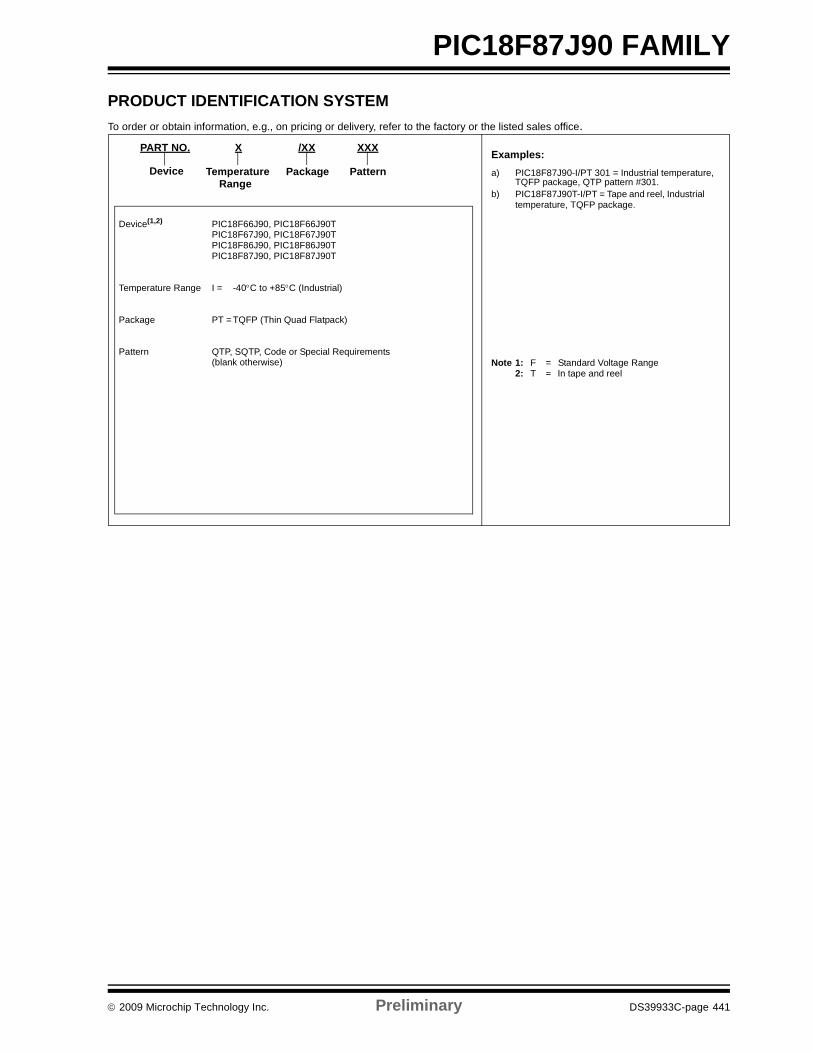
© 2009 Microchip Technology Inc. Preliminary DS39933C-page 441
PIC18F87J90 FAMILY
PRODUCT IDENTIFICATION SYSTEMTo order or obtain information, e.g., on pricing or delivery, refer to the factory or the listed sales office.
PART NO. X /XX XXX
PatternPackageTemperatureRange
Device
Device(1,2) PIC18F66J90, PIC18F66J90T
PIC18F67J90, PIC18F67J90TPIC18F86J90, PIC18F86J90TPIC18F87J90, PIC18F87J90T
Temperature Range I = -40°C to +85°C (Industrial)
Package PT = TQFP (Thin Quad Flatpack)
Pattern QTP, SQTP, Code or Special Requirements (blank otherwise)
Examples:a) PIC18F87J90-I/PT 301 = Industrial temperature,
TQFP package, QTP pattern #301.b) PIC18F87J90T-I/PT = Tape and reel, Industrial
temperature, TQFP package.
Note 1: F = Standard Voltage Range2: T = In tape and reel

DS39933C-page 442 Preliminary © 2009 Microchip Technology Inc.
AMERICASCorporate Office2355 West Chandler Blvd.Chandler, AZ 85224-6199Tel: 480-792-7200 Fax: 480-792-7277Technical Support: http://support.microchip.comWeb Address: www.microchip.comAtlantaDuluth, GA Tel: 678-957-9614 Fax: 678-957-1455BostonWestborough, MA Tel: 774-760-0087 Fax: 774-760-0088ChicagoItasca, IL Tel: 630-285-0071 Fax: 630-285-0075ClevelandIndependence, OH Tel: 216-447-0464 Fax: 216-447-0643DallasAddison, TX Tel: 972-818-7423 Fax: 972-818-2924DetroitFarmington Hills, MI Tel: 248-538-2250Fax: 248-538-2260KokomoKokomo, IN Tel: 765-864-8360Fax: 765-864-8387Los AngelesMission Viejo, CA Tel: 949-462-9523 Fax: 949-462-9608Santa ClaraSanta Clara, CA Tel: 408-961-6444Fax: 408-961-6445TorontoMississauga, Ontario, CanadaTel: 905-673-0699 Fax: 905-673-6509
ASIA/PACIFICAsia Pacific OfficeSuites 3707-14, 37th FloorTower 6, The GatewayHarbour City, KowloonHong KongTel: 852-2401-1200Fax: 852-2401-3431Australia - SydneyTel: 61-2-9868-6733Fax: 61-2-9868-6755China - BeijingTel: 86-10-8528-2100 Fax: 86-10-8528-2104China - ChengduTel: 86-28-8665-5511Fax: 86-28-8665-7889China - Hong Kong SARTel: 852-2401-1200 Fax: 852-2401-3431China - NanjingTel: 86-25-8473-2460Fax: 86-25-8473-2470China - QingdaoTel: 86-532-8502-7355Fax: 86-532-8502-7205China - ShanghaiTel: 86-21-5407-5533 Fax: 86-21-5407-5066China - ShenyangTel: 86-24-2334-2829Fax: 86-24-2334-2393China - ShenzhenTel: 86-755-8203-2660 Fax: 86-755-8203-1760China - WuhanTel: 86-27-5980-5300Fax: 86-27-5980-5118China - XiamenTel: 86-592-2388138 Fax: 86-592-2388130China - XianTel: 86-29-8833-7252Fax: 86-29-8833-7256China - ZhuhaiTel: 86-756-3210040 Fax: 86-756-3210049
ASIA/PACIFICIndia - BangaloreTel: 91-80-3090-4444 Fax: 91-80-3090-4080India - New DelhiTel: 91-11-4160-8631Fax: 91-11-4160-8632India - PuneTel: 91-20-2566-1512Fax: 91-20-2566-1513Japan - YokohamaTel: 81-45-471- 6166 Fax: 81-45-471-6122Korea - DaeguTel: 82-53-744-4301Fax: 82-53-744-4302Korea - SeoulTel: 82-2-554-7200Fax: 82-2-558-5932 or 82-2-558-5934Malaysia - Kuala LumpurTel: 60-3-6201-9857Fax: 60-3-6201-9859Malaysia - PenangTel: 60-4-227-8870Fax: 60-4-227-4068Philippines - ManilaTel: 63-2-634-9065Fax: 63-2-634-9069SingaporeTel: 65-6334-8870Fax: 65-6334-8850Taiwan - Hsin ChuTel: 886-3-572-9526Fax: 886-3-572-6459Taiwan - KaohsiungTel: 886-7-536-4818Fax: 886-7-536-4803Taiwan - TaipeiTel: 886-2-2500-6610 Fax: 886-2-2508-0102Thailand - BangkokTel: 66-2-694-1351Fax: 66-2-694-1350
EUROPEAustria - WelsTel: 43-7242-2244-39Fax: 43-7242-2244-393Denmark - CopenhagenTel: 45-4450-2828 Fax: 45-4485-2829France - ParisTel: 33-1-69-53-63-20 Fax: 33-1-69-30-90-79Germany - MunichTel: 49-89-627-144-0 Fax: 49-89-627-144-44Italy - Milan Tel: 39-0331-742611 Fax: 39-0331-466781Netherlands - DrunenTel: 31-416-690399 Fax: 31-416-690340Spain - MadridTel: 34-91-708-08-90Fax: 34-91-708-08-91UK - WokinghamTel: 44-118-921-5869Fax: 44-118-921-5820
WORLDWIDE SALES AND SERVICE
02/04/09