Embed Size (px)
Citation preview
Fast dynamic waveguides and waveguidearrays in photorefractive Sn2P2S6
induced by visible light
Flurin Juvalta, Roger Mosimann, Mojca Jazbinsek and Peter GunterInstitute of Quantum Electronics, ETH Zurich, CH-8093 Zurich (Switzerland)
Abstract: We report on dynamic waveguides and waveguide arraysinduced beneath the surface of electro-optic Sn2P2S6 crystals by visiblelight at 514 nm. The waveguide structures are generated by interbandphotoexcitation and drift or diffusion charge transport mechanism. Thesestructures are probed nondestructively in the transverse direction with abeam at a longer wavelength. We measured the fastest formation of lightinduced waveguides in the visible up to now. The recording times are below200 μs for intensities above 0.1 W/cm2. By interfering two light beams,dynamic waveguide arrays are generated with waveguide spacings of 7μm.If an electric field is applied to the crystal, these arrays can be spatiallyshifted by 1.5 μm for an applied field of E0 = 1 kV/cm.
© 2009 Optical Society of America
OCIS codes: (160.5320) Photorefractive materials; (230.7370) Waveguides
References and links1. P. Gunter, Nonlinear optical effects and materials (Springer 2000).2. D. Kip, M. Wesner, E. Kratzig, V. Shandarov, and P. Moretti, “All-optical beam deflection and switching in
strontium-barium-niobate waveguides,” Appl. Phys. Lett. 72, 1960–1962 (1998).3. J. Olivares, A. Garcia-Navarro, G. Garcia, A. Mendez, F. Agullo-Lopez, A. Garcia-Cabanes, M. Carrascosa, and
O. Caballero, “Nonlinear optical waveguides generated in lithium niobate by swift-ion irradiation at ultralowfluences,” Opt. Lett. 32, 2587–2589 (2007).
4. O. Matoba, T. Inujima, T. Shimura, and K. Kuroda, “Segmented photorefractive waveguides in LiNbO3:Fe,” J.Opt. Soc. Am. B 15, 2006–2012 (1998).
5. P. Dittrich, G. Montemezzani, P. Bernasconi, and P. Gunter, “Fast, reconfigurable light-induced waveguides,”Opt. Lett. 24, 1508–1510 (1999).
6. F. Juvalta, B. Koziarska-Glinka, M. Jazbinsek, G. Montemezzani, K. Kitamura, and P. Gunter, “Deep UV lightinduced, fast reconfigurable and fixed waveguides in mg doped LiTaO3,” Opt. Express 14, 8278–8289 (2006).
7. J. Petter and C. Denz, “Guiding and dividing waves with photorefractive solitons,” Opt. Comm. 188, 55–61(2001).
8. P. Zhang, J. L. Zhao, D. X. Yang, B. L. Li, and C. Xu, “Optically induced photorefractive waveguides inKNSBN:CE crystal,” Opt. Mat. 23, 299–303 (2003).
9. D. N. Christodoulides, F. Lederer, and Y. Silberberg, “Discretizing light behaviour in linear and nonlinear waveg-uide lattices,” Nature 424, 817–823 (2003).
10. J. W. Fleischer, M. Segev, N. K. Efremidis, and D. N. Christodoulides, “Observation of two-dimensional discretesolitons in optically induced nonlinear photonic lattices,” Nature 422, 147–150 (2003).
11. H. S. Eisenberg, Y. Silberberg, R. Morandotti, and J. S. Aitchison, “Diffraction management,” Phys. Rev. Lett.85, 1863–1866 (2000).
12. C. R. Rosberg, I. L. Garanovich, A. A. Sukhorukov, D. N. Neshev, W. Krolikowski, and Y. S. Kivshar, “Demon-stration of all-optical beam steering in modulated photonic lattices,” Opt. Lett. 31, 1498–1500 (2006).
13. J. W. Fleischer, G. Bartal, O. Cohen, T. Schwartz, O. Manela, B. Freedman, M. Segev, H. Buljan, and N. K.Efremidis, “Spatial photonics in nonlinear waveguide arrays,” Opt. Express 13, 1780–1796 (2005).
14. A. Shumelyuk, S. Odoulov, O. Oleynik, G. Brost, and A. A. Grabar, “Spectral sensitivity of nominally undopedphotorefractive Sn2P2S6,” Appl. Phys. B 88, 79–82 (2007).
(C) 2009 OSA 19 January 2009 / Vol. 17, No. 2 / OPTICS EXPRESS 379#98373 - $15.00 USD Received 10 Jul 2008; revised 30 Oct 2008; accepted 8 Dec 2008; published 5 Jan 2009
15. R. Mosimann, P. Marty, T. Bach, F. Juvalta, M. Jazbinsek, P. Gunter, and A. A. Grabar, “High-speed photorefrac-tion at telecommunication wavelength 1.55 μm in Sn2P2S6 :te,” Opt. Lett. 32, 3230–3232 (2007).
16. A. A. Grabar, M. Jazbinsek, A. Shumelyuk, Y. M. Vysochanskii, G. Montemezzani, and P. Gunter, “Photorefrac-tive effects in Sn2P2S6,” in Photorefractive Materials and Their Applications 2 , P. G. Huignard and J.-P., eds.,pp. 327–362 (Springer, 2007).
17. D. Haertle, G. Caimi, A. Haldi, G. Montemezzani, P. Gunter, A. A. Grabar, I. M. Stoika, and Y. M. Vysochanskii,“Electro-optical properties of Sn2P2S6,” Opt. Comm. 215, 333–343 (2003).
18. T. Bach, M. Jazbinsek, P. Gunter, A. A. Grabar, I. M. Stoika, and Y. M. Vysochanskii, “Self pumped opticalphase conjugation at 1.06 μm in te-doped Sn2P2S6,” Opt. Express 13, 9890–9896 (2005).
19. C. Dan, D. Wolfersberger, N. Fressengeas, G. Montemezzani, and A. A. Grabar, “Near infrared photorefractiveself focusing in Sn2P2S6:te crystals,” Opt. Express 16, 12777–12782 (2007).
20. G. Montemezzani, P. Rogin, M. Zgonik, and P. Gunter, “Interband photorefractive effects: Theory and experi-ments in KNbO3,” Phys. Rev. B 49, 2484–2502 (1994).
21. R. Mosimann, D. Haertle, M. Jazbinsek, G. Montemezzani, and P. Gunter, “Interband photorefraction in Sn2P2S6at visible wavelengths,” J. Opt. Soc. Am. B 23, 1620–1625 (2006).
1. Introduction
Waveguides are the basic elements in integrated optical applications [1]. Many of these applica-tions like optical switching, routing or dynamic optical interconnections require fast switchingbetween waveguide channels. This is normally done electro-optically by applying complicatedelectrode configurations on permanently structured waveguides [2,3]. Several techniques basedon light-induced refractive index changes have been recently proposed [4–9]. The most interest-ing feature of these waveguides is that they can be dynamically reconfigured, and thus signalscan be routed by solely changing the light illumination.
Periodic dielectric structures such as photonic crystals or photonic lattices have recentlygained a lot of interest due to their exciting features like controlling and manipulating thepropagation and manage the diffraction of optical beams [9–11]. In photorefractive crystals,a periodic modulation of the refractive index can be induced dynamically by interfering two ormore light beams inside the crystal. Beam steering in such a 1 dimensional optically inducedlattice has recently been demonstrated using a third controlling beam [12]. For investigationsof light propagation in periodic lattices, strontium-barium-niobate (SBN) is the most exten-sively employed material due to its high electro-optic activity (r33 = 235 pm/V for SBN:60,r33 = 1340 pm/V for SBN:75 at λ = 0.5 μm) [13]. However, the photorefractive response timesof SBN in the visible are in the order of a few seconds [13], which makes this material notsuitable for applications, where short waveguide formation times are required.
In this work, we investigate the potential of tin hypothiodiphosphate (Sn2P2S6) for dynamicwaveguide applications. Sn2P2S6 is a semiconducting ferroelectric material with interestingoptical and nonlinear optical properties: high photorefractive efficiency in the infrared up to thetelecommunication wavelength 1.55 μm [14–16] and a large electro-optic coefficient (r111 =174 pm/V at 633 nm [17]). Furthermore, the photorefractive response of Sn2P2S6 in the near-infrared is very fast, more than two orders of magnitude faster than in any other photorefractiveferroelectric crystal as e.g. Rh-doped BaTiO3 [18]. Recently, photorefractive self-focusing at1.06 μm was demonstrated in bulk Te doped Sn2P2S6 crystals with 15 ms response time at peakintensities of 160 W/cm2 [19].
The photorefractive response time can be decreased, if light with photon energy larger thanthe band gap of the material is used [20]. In this so-called interband photorefractive effect,refractive index structures can be generated by charge redistribution between the bands, whichin general provides 2-3 orders of magnitude faster response than the conventional effect.
So far, light induced waveguides were demonstrated in KNbO3 [5] and Mg doped LiTaO3 [6]by interband photorefraction with controlling light at ultraviolet (UV) wavelengths. However,there are some drawbacks of using UV light such as availability of laser sources, need of specialoptical elements and coatings to mention a few. Sn2P2S6 has a band gap energy of E = 2.3 eV,which is lower than in conventional photorefractive crystals and enables interband photorefrac-tion already in the visible at λ = 514 nm [21].
(C) 2009 OSA 19 January 2009 / Vol. 17, No. 2 / OPTICS EXPRESS 380#98373 - $15.00 USD Received 10 Jul 2008; revised 30 Oct 2008; accepted 8 Dec 2008; published 5 Jan 2009
In this work we show that fast reconfigurable waveguides and waveguide arrays can be in-duced beneath the surface of Sn2P2S6 crystals by using band-to-band excitations. The waveg-uiding structures are written beneath the surface in regions illuminated by 514 nm light by driftor diffusion of charge carriers, dominated by hole charge transport. They are probed nonde-structively in transverse direction.
2. Light induced waveguides
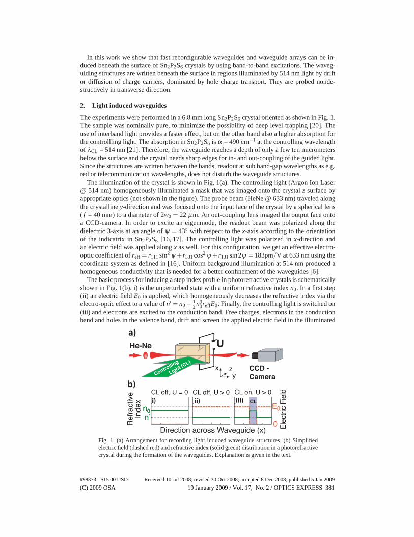
The experiments were performed in a 6.8 mm long Sn2P2S6 crystal oriented as shown in Fig. 1.The sample was nominally pure, to minimize the possibility of deep level trapping [20]. Theuse of interband light provides a faster effect, but on the other hand also a higher absorption forthe controllling light. The absorption in Sn2P2S6 is α = 490 cm−1 at the controlling wavelengthof λCL = 514 nm [21]. Therefore, the waveguide reaches a depth of only a few ten micrometersbelow the surface and the crystal needs sharp edges for in- and out-coupling of the guided light.Since the structures are written between the bands, readout at sub band-gap wavelengths as e.g.red or telecommunication wavelengths, does not disturb the waveguide structures.
The illumination of the crystal is shown in Fig. 1(a). The controlling light (Argon Ion Laser@ 514 nm) homogeneously illuminated a mask that was imaged onto the crystal z-surface byappropriate optics (not shown in the figure). The probe beam (HeNe @ 633 nm) traveled alongthe crystalline y-direction and was focused onto the input face of the crystal by a spherical lens( f = 40 mm) to a diameter of 2w0 = 22 μm. An out-coupling lens imaged the output face ontoa CCD-camera. In order to excite an eigenmode, the readout beam was polarized along thedielectric 3-axis at an angle of ψ = 43◦ with respect to the x-axis according to the orientationof the indicatrix in Sn2P2S6 [16, 17]. The controlling light was polarized in x-direction andan electric field was applied along x as well. For this configuration, we get an effective electro-optic coefficient of reff = r111 sin2 ψ +r331 cos2 ψ +r131 sin2ψ = 183pm/V at 633 nm using thecoordinate system as defined in [16]. Uniform background illumination at 514 nm produced ahomogeneous conductivity that is needed for a better confinement of the waveguides [6].
The basic process for inducing a step index profile in photorefractive crystals is schematicallyshown in Fig. 1(b). i) is the unperturbed state with a uniform refractive index n0. In a first step(ii) an electric field E0 is applied, which homogeneously decreases the refractive index via theelectro-optic effect to a value of n′ = n0− 1
2n30reffE0. Finally, the controlling light is switched on
(iii) and electrons are excited to the conduction band. Free charges, electrons in the conductionband and holes in the valence band, drift and screen the applied electric field in the illuminated
He-Ne
CCD -CameraContro
lling
Light (CL)
xy
z
Ele
ctric
Fie
ld
Ref
ract
ive
Inde
x
Direction across Waveguide (x)
CL off, U = 0 CL off, U > 0 CL on, U > 0CL
n0n0n’n’
E0
0
a)
i) ii) iii)
b)
Fig. 1. (a) Arrangement for recording light induced waveguide structures. (b) Simplifiedelectric field (dashed red) and refractive index (solid green) distribution in a photorefractivecrystal during the formation of the waveguides. Explanation is given in the text.
(C) 2009 OSA 19 January 2009 / Vol. 17, No. 2 / OPTICS EXPRESS 381#98373 - $15.00 USD Received 10 Jul 2008; revised 30 Oct 2008; accepted 8 Dec 2008; published 5 Jan 2009
CC
D -
Imag
es
x
z
FWHM: 50 µm FWHM: 12 µm
1 10 1000.1
1
Controlling-light Intensity ICL (mW/cm2)
Bui
ld-u
p T
ime
τ b
(ms)
τb ISlit-0.5
a)
b)
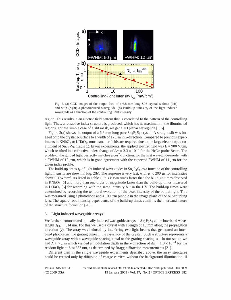
Fig. 2. (a) CCD-images of the output face of a 6.8 mm long SPS crystal without (left)and with (right) a photoinduced waveguide. (b) Build-up times τb of the light inducedwaveguide as a function of the controlling light intensity.
region. This results in an electric field pattern that is correlated to the pattern of the controllinglight. Thus, a refractive index structure is produced, which has its maximum in the illuminatedregions. For the simple case of a slit mask, we get a 1D planar waveguide [5, 6].
Figure 2(a) shows the output of a 6.8 mm long pure Sn2P2S6 crystal. A straight slit was im-aged onto the crystal z-surface to a width of 17 μm in x-direction. Compared to previous exper-iments in KNbO3 or LiTaO3, much smaller fields are required due to the large electro-optic co-efficient of Sn2P2S6 (Table 1). In our experiments, the applied electric field was E = 900 V/cm,which resulted in a refractive index change of Δn = 2.3×10⁻⁴ for the HeNe probe Beam. Theprofile of the guided light perfectly matches a cos2-function, for the first waveguide-mode, witha FWHM of 12 μm, which is in good agreement with the expected FWHM of 11 μm for thegiven index profile.
The build-up times τb of light induced waveguides in Sn2P2S6 as a function of the controllinglight intensity are shown in Fig. 2(b). The response is very fast, with τb < 200 μs for intensitiesabove 0.1 W/cm2. As listed in Table 1, this is two times faster than the build-up times observedin KNbO3 [5] and more than one order of magnitude faster than the build-up times measuredin LiTaO3 [6] for recording with the same intensity but in the UV. The build-up times weredetermined by recording the temporal evolution of the peak intensity of the output light. Thiswas measured using a photodiode and a 100 μm pinhole in the image plane of the out-couplinglens. The square-root intensity dependence of the build-up times confirms the interband natureof the structure formation [20].
3. Light induced waveguide arrays
We further demonstrated optically induced waveguide arrays in Sn2P2S6 at the interband wave-length λCL = 514 nm. For this we used a crystal with a length of 15 mm along the propagationdirection (y). The array was induced by interfering two light beams that generated an inter-band photorefractive grating beneath the z-surface of the crystal. Such a structure represents awaveguide array with a waveguide spacing equal to the grating spacing Λ . In our set-up wehad Λ ≈ 7 μm which yielded a modulation depth in the x-direction of Δn = 1.0×10⁻⁴ for thereadout light at λ ≈ 633 nm, as determined by Bragg diffraction measurements [21].
Different than in the single waveguide experiments described above, the array structurescould be created only by diffusion of charge carriers without the background illumination. If
(C) 2009 OSA 19 January 2009 / Vol. 17, No. 2 / OPTICS EXPRESS 382#98373 - $15.00 USD Received 10 Jul 2008; revised 30 Oct 2008; accepted 8 Dec 2008; published 5 Jan 2009
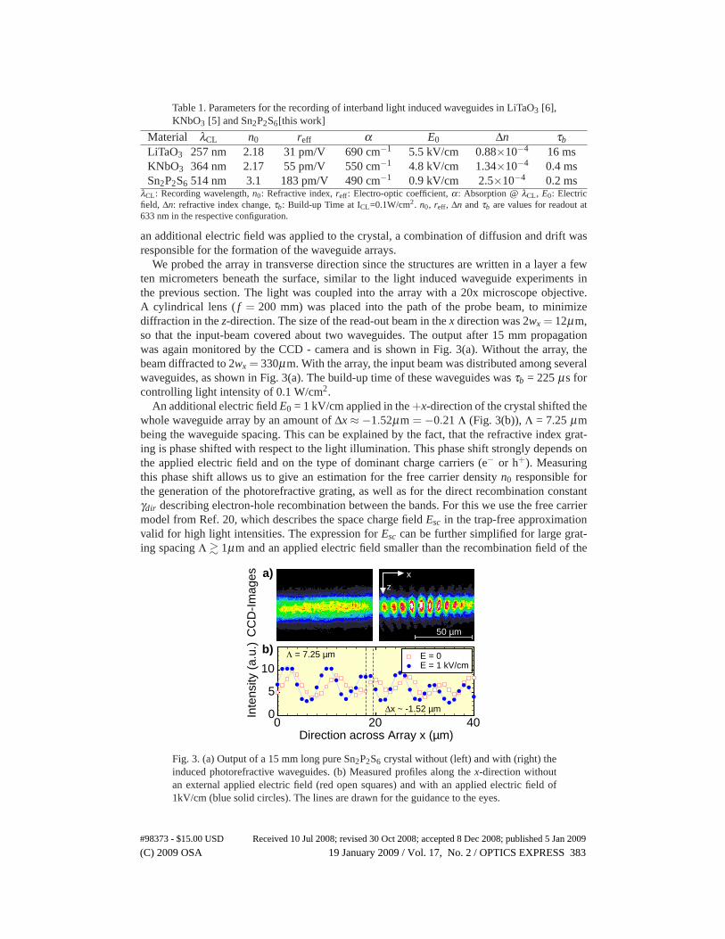
Table 1. Parameters for the recording of interband light induced waveguides in LiTaO3 [6],KNbO3 [5] and Sn2P2S6[this work]
Material λCL n0 reff α E0 Δn τb
LiTaO3 257 nm 2.18 31 pm/V 690 cm−1 5.5 kV/cm 0.88×10⁻⁴ 16 msKNbO3 364 nm 2.17 55 pm/V 550 cm−1 4.8 kV/cm 1.34×10⁻⁴ 0.4 msSn2P2S6 514 nm 3.1 183 pm/V 490 cm−1 0.9 kV/cm 2.5×10⁻⁴ 0.2 ms
λCL: Recording wavelength, n0: Refractive index, reff: Electro-optic coefficient, α: Absorption @ λCL, E0: Electricfield, Δn: refractive index change, τb: Build-up Time at ICL=0.1W/cm2. n0, reff, Δn and τb are values for readout at633 nm in the respective configuration.
an additional electric field was applied to the crystal, a combination of diffusion and drift wasresponsible for the formation of the waveguide arrays.
We probed the array in transverse direction since the structures are written in a layer a fewten micrometers beneath the surface, similar to the light induced waveguide experiments inthe previous section. The light was coupled into the array with a 20x microscope objective.A cylindrical lens ( f = 200 mm) was placed into the path of the probe beam, to minimizediffraction in the z-direction. The size of the read-out beam in the x direction was 2wx = 12μm,so that the input-beam covered about two waveguides. The output after 15 mm propagationwas again monitored by the CCD - camera and is shown in Fig. 3(a). Without the array, thebeam diffracted to 2wx = 330μm. With the array, the input beam was distributed among severalwaveguides, as shown in Fig. 3(a). The build-up time of these waveguides was τb = 225 μs forcontrolling light intensity of 0.1 W/cm2.
An additional electric field E0 = 1 kV/cm applied in the +x-direction of the crystal shifted thewhole waveguide array by an amount of Δx ≈−1.52μm = −0.21 Λ (Fig. 3(b)), Λ = 7.25 μmbeing the waveguide spacing. This can be explained by the fact, that the refractive index grat-ing is phase shifted with respect to the light illumination. This phase shift strongly depends onthe applied electric field and on the type of dominant charge carriers (e− or h+). Measuringthis phase shift allows us to give an estimation for the free carrier density n0 responsible forthe generation of the photorefractive grating, as well as for the direct recombination constantγdir describing electron-hole recombination between the bands. For this we use the free carriermodel from Ref. 20, which describes the space charge field Esc in the trap-free approximationvalid for high light intensities. The expression for Esc can be further simplified for large grat-ing spacing Λ � 1μm and an applied electric field smaller than the recombination field of the
0 20 400
5
10
Direction across Array x (µm)
Inte
nsity
(a.
u.)
Δx ~ -1.52 µm
Λ = 7.25 µm
CC
D-I
mag
es xz
a)
b)
50 µm
E = 0E = 1 kV/cm
Fig. 3. (a) Output of a 15 mm long pure Sn2P2S6 crystal without (left) and with (right) theinduced photorefractive waveguides. (b) Measured profiles along the x-direction withoutan external applied electric field (red open squares) and with an applied electric field of1kV/cm (blue solid circles). The lines are drawn for the guidance to the eyes.
(C) 2009 OSA 19 January 2009 / Vol. 17, No. 2 / OPTICS EXPRESS 383#98373 - $15.00 USD Received 10 Jul 2008; revised 30 Oct 2008; accepted 8 Dec 2008; published 5 Jan 2009
dominant charge carriers, i.e. the average internal electric field in which the charges drift foran average distance K−1 = Λ/2π before recombination. In our configuration this is true forE0 � 20 kV/cm considering the results of the Bragg diffraction measurements [21]. We fur-thermore consider only one type of charge carriers. This is eligible if one of the mobilities ismuch larger than the other one, i.e. μe � μh or μh � μe for electron or hole dominated chargetransport respectively. This simplification yields the following relation for the space chargefield:
Esc ≈ imEq f (∓ED + iE0)
2Eq f ∓ iE0(1)
where ED = KkBT/e is the diffusion field and Eq f = eεε0K n0 is the maximum electric field that
can be created by free charge carriers; m grating modulation depth, kB Boltzmann constant,T absolute temperature, e elementary charge, ε0 vacuum permittivity and ε = 230 [16] thedielectric constant of Sn2P2S6. The upper signs in Eq. (1) are for electron and the lower signsfor hole dominated charge transport respectively. The phase shift φ between the waveguidearray and the interference pattern can then be calculated from Eq. (1) and is given by:
tanφ ≈± 2Eq f ED +E20
2Eq f E0 −EDE0. (2)
Taking into account the negative sign of the electro-optic effect (Δn ∝ −E), positive and neg-ative values of φ correspond to dominant electron and hole charge transport respectively. Thespatial shift of the array in the negative x direction after applying an electric field to the arrayimplies a reduced negative phase shift in our experiment. This proves that the hole mobility inour Sn2P2S6 crystal is larger than the electron mobility, in agreement with two-wave mixingexperiments at this wavelength [21].
Without applied electric field, a maximum shift of φ0 = −π2 is reached. After applying an
electric field of E0 = 1 kV/cm, the array is phase shifted by φE = 1.32 rad. This correspondsto a phase shift of φ = φE + φ0 = −0.25 rad between the array and the light fringes. Usingthe above definitions of ED and Eq f , the charge density can be estimated from Eq. (2) ton0 ≈ 2· 1016 cm−3 for a writing light intensity of I0 = 100 mW/cm2. Assuming a quantum effi-ciency close to 1, we can give an estimation for the direct recombination constant of Sn2P2S6:γdir = αI0/(hνn2
0) ≈ 4· 10−13 cm3s−1, with absorption constant α and photon energy hν .By applying a modulating electric field, it may be possible to modulate such arrays in real-
time. The arrays may also be shifted by a modulated phase-difference between the two writingbeams, which can be realized with an additional electro-optic modulator or a piezo-controlledmirror in the path of one of the writing beams, as used for moving photorefractive gratings [15].
4. Conclusions
We have demonstrated for the first time to our knowledge waveguides and waveguide ar-rays induced by band-to-band excitation at visible wavelengths. In the electro-optic materialSn2P2S6 we measured the fastest build-up of light induced waveguide structures (τ = 200 μsat I0 = 0.1 W/cm2) reported up to now. This is more than four orders of magnitude faster thanfor previously studied waveguides induced at visible wavelengths, which were produced bythe conventional potorefractive effect [13]. The presented technique allows the generation ofdifferent straight and bent dynamic waveguide structures by using external masks or a spatiallight modulator. Due to the fast response of Sn2P2S6, these structures can be reconfigured in asub-millisecond time-scale.
Acknowledgments
We thank J. Hajfler for his expert crystal preparation and I. M. Stoika and A. A. Grabar forthe growth of the crystals. This research has been supported by the Swiss National ScienceFoundation.
(C) 2009 OSA 19 January 2009 / Vol. 17, No. 2 / OPTICS EXPRESS 384#98373 - $15.00 USD Received 10 Jul 2008; revised 30 Oct 2008; accepted 8 Dec 2008; published 5 Jan 2009