Embed Size (px)
Citation preview

Fast Optical Readout of the Mu3ePixel Detector
Master Thesis
Simon Corrodi
March, 2014
Advisors:
Dr. Niklaus Berger
Department of Physics and Astronomy, Heidelberg University
Prof. Dr. Gunther Dissertori
Department of Physics, ETH Zurich
Zusammenfassung
Das Mu3e Experiment sucht nach dem Lepton-Flavour-verletzenden Zerfall µ+ →e+e−e+ mit einer Sensitivitat von besser als 1 in 1016 µ-Zerfallen. Um diese Sen-sitivitat zu erreichen, sind uber eine Messzeit von ca. 1 Jahr 2 Milliarden Zerfallepro Sekunde notwendig. Die Trajektorien der Zerfallsprodukte werden von Pixel-,szintillierenden Faser- und Kacheldetektoren gemessen und in Echtzeit in einer aufGrafikprozessoren basierenden Filterfarm komplett rekonstruiert. Der fur die schnelleAuslese der Daten im Detektor vorhandene Platz ist stark limitiert.
Das auf Kapton Flexprints, optischen Fasern und FPGAs basierende Auslesesys-tem verarbeitet 1 Tbit/s auf engstem Raum.
In der vorliegenden Arbeit wurden optische Verbindungen in Kombination mitFPGA Baugruppen auf ihre Bandbreiten bei moglichst kleinen Fehlerraten getestet.
Bidirektionale Ubertragungen mit 8 simultan genutzten Kanalen auf einer FPGATochterkarte mit SFP Steckern sind mit Fehlerraten unter < 10−16 (95 % C.L.) bei6.4 Gbit/s realisiert worden. Optische Verbindungen im QSFP Standard konnenmit einer Fehlerrate von (3.29 ± 1.04) · 10−16 bei 11.3 Gbit/s betrieben werden.Die optischen Datenubertragungen erfullen die Anforderungen, die an das Mu3eAuslesesystems gestellt werden.
Zusatzlich wurde gezeigt, dass Kapton Flexprints grundsatzlich mit einem neuangeschafften Laserplotter an der Universitat Heidelberg produziert werden konnten.
Abstract
The Mu3e experiment searches for the lepton flavor violating decay µ+ → e+e−e+
with a sensitivity better than 1 in 1016 µ-decays. To reach this sensitivity in a mea-surement period of approximately 1 year, 2 billion decays per seconds are required.The decay products’ trajectories are measured by pixel, scintillating fibers and tiledetectors and fully reconstructed online by a filter farm based on graphics processingunits. The available space inside the detector for the fast data readout is stronglylimited.
The readout system based on Kapton flexprints, optical fibers and FPGAs pro-cesses 1 Tbit/s in a very compact volume.
In the presented work, optical links in combination with FPGA boards are testedwith respect to their bandwidths at minimal bit error rates.
Eight parallel duplex 6.4 Gbit/s links on one FPGA daughter board equippedwith SFP plugs have been realized with bit error rates below < 10−16 (95 % C.L.).Optical links in QSFP standard have been operated at 11.3 Gbit/s with bit errorrates of (3.29± 1.04) · 10−16. The optical data transmissions fulfill the requirementsfor the Mu3e data acquisition system.
In addition, it has been proven that Kapton flexprints can be manufactured inprinciple with a new purchased laser cutting system at the University of Heidelberg.
i

Contents
Contents ii
I Introduction 1
1 Introduction 21.1 The Standard Model . . . . . . . . . . . . . . . . . . . . . . . . . . . 2
1.1.1 Lepton Flavour Violating (Muon) Decays . . . . . . . . . . . 31.2 The Mu3e Experiment . . . . . . . . . . . . . . . . . . . . . . . . . . 51.3 Mu3e Readout Concept . . . . . . . . . . . . . . . . . . . . . . . . . 8
1.3.1 Pixel to Front-End Links . . . . . . . . . . . . . . . . . . . . 91.3.2 Front-End FPGA . . . . . . . . . . . . . . . . . . . . . . . . . 101.3.3 Detector to Counting House Links . . . . . . . . . . . . . . . 111.3.4 Read-out FPGAs . . . . . . . . . . . . . . . . . . . . . . . . . 111.3.5 GPU Filter Farm . . . . . . . . . . . . . . . . . . . . . . . . . 12
II Basics of Data Transmission 13
2 Physical Layer 142.1 Signal propagation . . . . . . . . . . . . . . . . . . . . . . . . . . . . 14
2.1.1 Electrical Conductors . . . . . . . . . . . . . . . . . . . . . . 142.1.2 Optical Wave Guides . . . . . . . . . . . . . . . . . . . . . . . 15
2.2 Encoding Schemes . . . . . . . . . . . . . . . . . . . . . . . . . . . . 152.2.1 Line Codes . . . . . . . . . . . . . . . . . . . . . . . . . . . . 162.2.2 Running Disparity . . . . . . . . . . . . . . . . . . . . . . . . 172.2.3 Scrambling . . . . . . . . . . . . . . . . . . . . . . . . . . . . 192.2.4 Protocols . . . . . . . . . . . . . . . . . . . . . . . . . . . . . 19
2.3 Signal Quality Check . . . . . . . . . . . . . . . . . . . . . . . . . . . 232.3.1 Eye Diagrams . . . . . . . . . . . . . . . . . . . . . . . . . . . 232.3.2 Bathtub Diagrams . . . . . . . . . . . . . . . . . . . . . . . . 232.3.3 Cyclic Redundancy Checks (CRC) . . . . . . . . . . . . . . . 25
3 Electronic Components 273.1 Logic Gates . . . . . . . . . . . . . . . . . . . . . . . . . . . . . . . . 273.2 Memory Elements . . . . . . . . . . . . . . . . . . . . . . . . . . . . 27
3.2.1 Flip-Flops . . . . . . . . . . . . . . . . . . . . . . . . . . . . . 273.2.2 Random-Access Memory (RAM) . . . . . . . . . . . . . . . . 28
ii

3.2.3 First In First Out (FIFO) . . . . . . . . . . . . . . . . . . . . 283.2.4 Read-Only Memory ROM . . . . . . . . . . . . . . . . . . . . 28
3.3 Phase Locked Loop (PLL) . . . . . . . . . . . . . . . . . . . . . . . . 283.3.1 Clock Data Recovery (CDR) . . . . . . . . . . . . . . . . . . 29
3.4 Linear Feedback Shift Register (LFSR) . . . . . . . . . . . . . . . . . 293.4.1 Pseudo Random Number Generators (PRN) . . . . . . . . . . 293.4.2 Counter . . . . . . . . . . . . . . . . . . . . . . . . . . . . . . 293.4.3 Other Uses . . . . . . . . . . . . . . . . . . . . . . . . . . . . 30
3.5 Gray Counter . . . . . . . . . . . . . . . . . . . . . . . . . . . . . . . 30
4 Field Programmable Logic Gates (FPGA) 31
III Measurements 33
5 Optical Links 345.1 Soft- and Hardware . . . . . . . . . . . . . . . . . . . . . . . . . . . . 34
5.1.1 Altera Stratix V Development Kit . . . . . . . . . . . . . . . 345.1.2 SantaLuz Mezzanine Board . . . . . . . . . . . . . . . . . . . 375.1.3 Plugs . . . . . . . . . . . . . . . . . . . . . . . . . . . . . . . 375.1.4 Cables . . . . . . . . . . . . . . . . . . . . . . . . . . . . . . . 39
5.2 Firmware . . . . . . . . . . . . . . . . . . . . . . . . . . . . . . . . . 405.2.1 Data Transmission State Machine . . . . . . . . . . . . . . . 405.2.2 Bit Error Rate Tests (BERT) . . . . . . . . . . . . . . . . . . 425.2.3 Altera Receiver Toolkit . . . . . . . . . . . . . . . . . . . . . 44
5.3 Measurements . . . . . . . . . . . . . . . . . . . . . . . . . . . . . . . 465.3.1 BER Upper Limit and Error Calculations . . . . . . . . . . . 465.3.2 Optical SFP Links . . . . . . . . . . . . . . . . . . . . . . . . 485.3.3 Single Channel SFP . . . . . . . . . . . . . . . . . . . . . . . 505.3.4 Multi-Channel SFP . . . . . . . . . . . . . . . . . . . . . . . 555.3.5 Optical QSFP Links . . . . . . . . . . . . . . . . . . . . . . . 60
5.4 Discussion . . . . . . . . . . . . . . . . . . . . . . . . . . . . . . . . . 615.4.1 Summary . . . . . . . . . . . . . . . . . . . . . . . . . . . . . 625.4.2 Crucial Points . . . . . . . . . . . . . . . . . . . . . . . . . . 63
6 Readout Chain Firmware Components 656.1 Front-End FPGA . . . . . . . . . . . . . . . . . . . . . . . . . . . . . 65
6.1.1 Hit Data Structure . . . . . . . . . . . . . . . . . . . . . . . . 656.1.2 Concept I . . . . . . . . . . . . . . . . . . . . . . . . . . . . . 666.1.3 Concept II . . . . . . . . . . . . . . . . . . . . . . . . . . . . 666.1.4 Comparison . . . . . . . . . . . . . . . . . . . . . . . . . . . . 66
6.2 Coordinate Transformation on FPGAs . . . . . . . . . . . . . . . . . 666.2.1 Coordinate Systems . . . . . . . . . . . . . . . . . . . . . . . 676.2.2 The Transformation . . . . . . . . . . . . . . . . . . . . . . . 686.2.3 The Implementation . . . . . . . . . . . . . . . . . . . . . . . 686.2.4 Performance . . . . . . . . . . . . . . . . . . . . . . . . . . . 706.2.5 Conclusion . . . . . . . . . . . . . . . . . . . . . . . . . . . . 70
iii
7 LVDS on Kapton FlexPrints 717.1 Kapton . . . . . . . . . . . . . . . . . . . . . . . . . . . . . . . . . . 717.2 Low-Voltage Differential Signaling (LVDS) . . . . . . . . . . . . . . . 717.3 Laser Platform . . . . . . . . . . . . . . . . . . . . . . . . . . . . . . 727.4 Proof of Concept . . . . . . . . . . . . . . . . . . . . . . . . . . . . . 737.5 Future Work . . . . . . . . . . . . . . . . . . . . . . . . . . . . . . . 75
IV Outlook 76
8 Outlook 778.1 Readout Chain in General . . . . . . . . . . . . . . . . . . . . . . . . 778.2 Data Structure . . . . . . . . . . . . . . . . . . . . . . . . . . . . . . 77
8.2.1 Starting Point . . . . . . . . . . . . . . . . . . . . . . . . . . 778.2.2 Error Detection . . . . . . . . . . . . . . . . . . . . . . . . . . 788.2.3 Proposed Format . . . . . . . . . . . . . . . . . . . . . . . . . 78
8.3 Phase Ia Readout Chain . . . . . . . . . . . . . . . . . . . . . . . . . 78
A Appendix 80A.1 Stratix V Transceivers . . . . . . . . . . . . . . . . . . . . . . . . . . 80
A.1.1 Physical Media Attachment (PMA) . . . . . . . . . . . . . . 80A.1.2 Physical Coding Sublayer (PCS) . . . . . . . . . . . . . . . . 82
A.2 Quartus II and ModelSim . . . . . . . . . . . . . . . . . . . . . . . . 85A.2.1 ModelSim . . . . . . . . . . . . . . . . . . . . . . . . . . . . . 86
A.3 Multi-Channel Results . . . . . . . . . . . . . . . . . . . . . . . . . . 88A.4 MuPix4 Emulator . . . . . . . . . . . . . . . . . . . . . . . . . . . . 88A.5 SantaLuz Crosstalk Measurments . . . . . . . . . . . . . . . . . . . . 89A.6 MuPix Address Scheme . . . . . . . . . . . . . . . . . . . . . . . . . 90
List of Figures 92
List of Tables 94
Bibliography 95
Acknowledgements 99
iv

Part I
Introduction
1

Chapter 1
Introduction
The Standard Model (SM) of particle physics describes the constituents of matteras well as their interactions. It is described in more detail in a first section, followedby the observation of lepton flavor violation through neutrino oscillations and itsconsequences for the theory. These motivate the search of lepton flavor violatingprocesses in charged leptons as described in another section.
The Mu3e experiment looks for the charged lepton flavour violating decay µ →eee. In a second chapter, the design of this experiment is discussed. Particularly,the experiment’s readout chain, the main scope of this thesis, is presented in detail.
1.1 The Standard Model
The Standard Model (SM) of particle physics is a quantum field theory which de-scribes the fundamental constituents and interactions of matter. As shown in figure1.1, matter consists of six quarks and six leptons, and their anti-particles, whichare arranged in three generations. The interactions between quarks and leptons aremediated by four types of gauge bosons.
The first generation consists of up (u) and down (d) quarks with electrical chargesof +2/3 and −1/3 respectively , the negatively charged electron (e−) and the neutralneutrino (νe). The lepton family number Le is characteristic for the leptons of thisfamily. The second and third generation consist both in each case of two quarks withthe same charge as the first generation - these are charm (c) and strange (s) in thesecond and top (t) and bottom (b) in the third generation. Their associated leptons,again with the same electrical charge as the ones in the first generation, are muons(µ−) and the neutrino (νµ), tau (τ) and the neutrino (ντ ). Their characteristiclepton family numbers are Lµ and Lτ . In the SM neutrinos are massless and leptonflavour is a conserved quantity.
Quarks and leptons are spin 1/2 particles whose interaction is mediated by spin 1particles, the gauge bosons. The eight gluons mediate the strong interaction, photons(γ) the electromagnetic interaction and Z , W+ and W− bosons the weak force.
The model has demonstrated huge and continued successes, particularly the re-cent discovery of the long predicted higgs boson in 2012 [1] at the LHC. Gravitationis not included in the standard model [2, 3].
2
Figure 1.1: Standard Model Particles [4, modified ].
Lepton Flavour Violation
Different experiments have observed mixing of neutrino flavours. Super-Kamiokandeand others have observed [5] mixing in atmospheric and solar neutrinos, SNO [6] insolar neutrinos and KamLAND [7] in reactor neutrinos. The mixing angles in thePontecorvo Maki Nakagawa Sakata (PMNS) matrix, the matrix which describes theneutrino mixing, are close to maximal [8].
Neutrino oscillation is only possible if neutrinos have a non-vanishing mass, whichis not foreseen in the SM. An extension of the Minimal Standard Model by heavyright-handed neutrinos, called νSM, is required to incorporate neutrino masses con-sistent with oscillation experiments. The reason why the neutrino masses are signif-icantly smaller than other particle’s masses remains a puzzle [9].
Even though the PMNS matrix appears also in charged lepton currents, leptonflavour violation has never been observed in charged leptons. These flavour-changingneutral currents are suppressed by a mechanism described by Glashow, Iliopoulosand Maiani in 1970 [10].
Also, the νSM is not able to explain all observations such as dark matter, thebaryon asymmetry of the universe or motivate the observation of exactly three gen-erations of particles. This motivates theories beyond the standard model (BSM).Several of these, like supersymmetry or little Higgs models among others, predictlarge lepton flavour violation in the charged lepton sector.
Due to the fact that flavour violating processes in the charged leptonic sector arehighly suppressed in νSM and predicted in many BSM theories, these processes arevery interesting to search for BSM physics.
1.1.1 Lepton Flavour Violating (Muon) Decays
The lepton flavour violating (LFV) muon decay µ+ → e+e−e+ can be realised inextensions of Standard Models which include lepton mixing. Figure 1.2 shows thisFeynman diagram with neutrino oscillation. The W+ mass of 80.4 GeV/c2 is much
3

higher than the neutrino masses of O(0.01eV ), hence the process is suppressed by a
factor of ∼(
∆m2
m2
W+
)2
which is of the order ≪ 10−50.
Figure 1.2: Feynman diagram for the µ → eee process via neutrino mixing [11, Fig.2.1].
(a) involving supersymmetric particles (b) at tree level
Figure 1.3: Diagram for lepton flavour violation [11, Fig. 2.2,2.3].
BSM theories can introduce new possible diagrams, particularly loop contribu-tions and new tree couplings. Figure 1.3a shows a diagram with a γ/Z-penguin witha supersymmetric particle in the loop, where LFV is introduced by slepton mixing.Figure 1.3b shows a diagram, where lepton flavour violation occurs on tree level vianew heavy particles, coupling to both electrons and muons [11].
As described before, the process µ → eee is sensitive to new physics and sup-pressed in the νSM. In contrast to µ→ eγ, it is also sensitive to tree level processes.
Experimental Situation
The current upper limit of B(µ → eee) < 10−12 at a 95% C.L. was set in 1988 bythe SINDRUM experiment at PSI [13] .
Other decays such as µ → eγ measured by MEG in 2009 to 2011 with B(µ →eγ)< 5.7 · 10−13 (90% C.L.) [14] and conversions in presence of a nucleus µN → eNas measured by SINDRUM II with B(µ→ e conversion in 27Al) < 7 · 10−13 are alsosensitive to charged LFV.
For loop correction diagrams, MEG’s sensitivity is two orders of magnitude higherdue to the additional photon electron-positron vertex in µ → eee. But the experi-ment is not sensitive at all for tree level processes. Conversion processes are sensitiveto both described types of diagrams and their sensitivity scales ∼ Z2 [15, Figure 2-5,2-6]. Figure 1.4 gives an overview over previously performed measurements in thesearch for LFV in charged leptons.
4

Figure 1.4: History of LFV measurements. Modified [12].
Backgrounds for a µ→ eee search
On one hand, background due to internal conversion µ → eeeνν with a branchingratio of 3.4 · 10−5 [16], and on the other hand accidental background is present. Ac-cidental background consists of a combination of events which produce one positronand an overlying electron-positron pair.
The internal conversion can only be resolved by a very good energy resolution,which is able to resolve the missing energy due to the additional neutrinos. Micheldecays µ+ → e+νν, radiative muon decays µ+ → e+γνν with a branching ratioof 1.4 · 10−2 and Bhabha scattered electrons contribute to accidentals. They aresuppressed through good vertex fits and time resolution.
The pion decay π → eeeν with a branching fraction of 3.2 · 10−9 [16] is indis-tinguishable if the right momentum is met. A low pion contamination in the beam,small branching ratio and small probability to meet the right momentum suppressesthis background source strongly.
1.2 The Mu3e Experiment
The Mu3e experiment searches for the lepton flavour violating decay µ+ → e+e−e+.It aims for an ultimate sensitivity of one in 1016 µ-decays. The experiment uses novelthinned silicon pixel sensors for high spatial resolution and scintillating fibres as wellas scintillating tiles for high timing resolution. These technologies combined with adetector design for highest possible momentum resolution allow a background sup-pression below the targeted ∼ 10−16. To perform the measurement in a reasonabletime scale, very high muon decay rates are needed. These high muon rate and back-
5

ground suppression are the main challenges for the experiment and define, togetherwith a desired high acceptance, the design.
To suppress background events, a precise vertex fitting, better than 200 µm,momentum measurements, better than 0.5MeV/c, and timing resolution, better than100 ps, are required. Therefore, the material inside the detector is reduced to below1 h of a radiation length to minimize scattering. Furthermore, the innermost layersare very close to the target to improve vertex resolution.
In the experiment, muons decay at rest, hence the maximal available momentumis 53MeV/c. Because no calorimeter is needed, a very compact detector design isfavourable to detect on one hand electrons with a momentum as low as 10MeV/c. Onthe other hand, electrons with a higher momentum are measured with high precisionas recurlers after almost one full cycle in the 1 Tesla magnetic field. Additionalscintillating fibers and tiles provide very precise timing information, which is neededfor background suppression particularly at high rates. For a design as shown in figure1.5 with a pixel size of 80x80 µm the momentum resolution is multiple scatteringdominated.
The detector is composed of up to five 36 cm long cylinders with an outer diameterof 17 cm surrounded by a magnet and its shielding. To provide enough free spacefor recurling electrons of up to 53MeV/c the minimal distance of the magnet tothe experiment’s central axis can not be smaller than 50 cm. For cooling the wholedetector volume is flushed with gaseous helium with a flow of several m/s.
The detector will be built in phases. A first phase, called Ia, is composed onlyof the inner and outer layers of the center pixel sensors element. In phase Ib thescintillating fibers and recurl stations are added. Phase I will be operated with amaximum muon rate of 2 ·108 Hz. For phase II one additional recurl station on eachside as well as tile sub-detectors will be added to handle rates up to 2 · 109 µ/s.
Muon Production and Stopping At the Paul Scherrer Institute (PSI) in Switzer-land, a cyclotron produces a 2.4mA proton beam with particle momenta of 590MeV/c.The proton beam hits a graphite target rotating with 1Hz, producing pions whichdecay on the surface to muons. The proton beam bulk remains and is shot to aspallation neutron target, which is built from lead-filled zircaloy tubes.
For phase I, the πE5 channel at PSI provides 28 MeV/c muons at a rate of 108
µ/s produced in target E. Their momentum is very close to the kinematic-edge ofstopped pion decay and hence close to the maximum production rate. These muonscan be stopped efficiently in the thin Mu3e target. For phase II, a new beam linealso at PSI is being planned, the high intensity muon beamline (HiMB). The HiMBextracts muons produced at the existing spallation neutron target. This new beamis supposed to deliver up to 3 · 1010 µ/s, 2 · 109 µ/s are needed for Mu3e.
In the Mu3e detector, the polarized muons are stopped in a 100 mm long hollowdouble cone target with a maximum diameter of 20 mm. The front cone is made of30 µm and the back one of 80 µm aluminum.
Pixel Detector The Mu3e pixel tracker, here after called the MuPix sub-detector,is built from High-Voltage Monolithic Active Pixel Sensors (HV-MAPS) thinnedto 50 µm [17]. The sensors are held by a Kapton support structure. Aluminumtraces on Kapton flex-prints supply the chips and provide fast serial data links. The150 mW/cm2 heat from the sensors is cooled with a global gaseous helium flow aswell as by small helium tubes in the support structure.
6

(a) Phase 1a: Only central pixel detector.
(b) Phase 1b: Added scintillating fibers and tiles, one recurl station on each side.
(c) Phase 2: Additional recurl stations on each side.
Figure 1.5: Mu3e experiment setup overview. Phase I consists of inner layer andcorresponding outer layer including the fiber sub-detector. Phase II adds a recurlerstation on each side with pixel and tile sub-detectors. In (b) on the right side afront view with recurling electron and respectively positron tracks is shown [11].
7

In classical MAPS designs, ionization charges are collected by diffusion witha time constant of several hundred nanoseconds. Applying a high bias voltage,introduces charge collection by drift and increases the time resolution to the order of10 ns. Deep N-wells allow to place the complete electronics inside the pixels. The perpixel electronics are accompanied by a per sensor digital serial readout part. Thepixel sensors provide zero-suppressed hit information with an associated 20 MHzGray code timestamp. HV-MAPS are produced in a standard technology mainlyused in the automotive industry, AMS/IBM 180 nm HV-CMOS. Thinning siliconwafers down to 50 µm is also a standard procedure.
Two different types of sensors are used for the inner and the outer layers. Bothhave pixel sizes of 80 x 80 µm2, the inner sensors have a size of 1.1 x 2 cm2 and areequipped with three serial output lines, whereas the outer ones have a size of 2 x 2cm2 and provide only one line [18, 19].
Fiber Detector The pixel sub-detector’s hit information is read out in 50 nsframes. To be able to handle rates up to 2 · 109 decays per second, which results inup to 100 tracks per frame, more precise timing information is needed. A scintillatingfibre (Sci-Fi) hodoscope with a length of 36 cm and a radius of 6 cm and a timingresolution of 1 ns partly solves the problem. The fibers are a trade-off between aminimal material budget to decrease scattering and an efficient readout. Ribbonswith three layers of 250µm round fibers as well as 2 layers of 250µm square fibers areunder discussion. The light produced in the scintillating fibers is detected by siliconphoto multipliers (SiPM) mounted at both ends of the ribbons. These devices arevery compact, have a high gain factor and are insensitive to the presence of magneticfields. They can be operated at very high rates [20].
Tile Detector The timing measurement in the recurl stations is performed withscintillating tiles right inside the pixel layers. Since this is the last measurementperformed on the particles, more material can be used. The tiles achieve a timeresolution of ≈ 0.1 ns and an efficiency close to 100%. Like the scintillating fibersthey are read-out with SiPMs [21, 22].
Detector Environment All the above described elements of the detector areplaced inside a homogeneous solenoid 1T magnetic field. The whole detector volumeis flushed for cooling with gaseous helium supplied by helium cooling channels insidethe Kapton base structure. The read-out electronics is placed up- and down-streamdirectly on the beam pipe, which is cooled through embedded channels for liquidcoolant [23]. Figure 1.6 shows a rendering of the phase 1 detector and shows thelimited space available for readout electronics.
1.3 Mu3e Readout Concept
The Mu3e readout chain is designed in such a way that every graphic processing unit(GPU) in a filter farm receives data of the entire detector, but only of a small timeslice. The raw data from all sub-detectors are buffered, ordered, bundled, merged,routed and transformed in the data acquisition system. Data reduction takes placeonly at the last node through complete track and event reconstruction. Finally, onlyselected events are stored.
8

Figure 1.6: Mu3e phase 1 detector rendering with 4 layers of pixel detector, beampipe and electronics in green. The available space for readout electronic is highlylimited.
Figure 1.7 shows a data flow overview with focus on the MuPix sub-detector.MuPix pixel chips send zero-suppressed data over LVDS links to a front-end FPGA.The received hit data is time ordered, merged and routed via optical links to a read-out FPGA which routes it further on to a standard PC in the filter farm. Differentsub-detectors are processed with separate read-out FPGAs. The third FPGA inthe chain transforms the hit data into global coordinates and puts it through directmemory access (DMA) into a powerful GPU. Online event reconstruction is per-formed and selected events are stored. Slow control information is sent via the samelinks from a controller over read-out and front-end FPGA to the pixel detector.
Data links in Mu3e handle O(1 Tbit/s) through different technologies. Thecomponents required to handle this rate are shown in figure 1.8, in phase Ia onlysubfarm A is needed. The data from 1116 pixel sensors are divided into up- anddown-stream and collected in 38 front-end FPGAs with 45 or 36 links each. The up-and downstream data sets are collected in two readout FPGAs, which deliver fulldetector information of a time slice to one of 12 PCs in the filter farm. Each PC isequipped with one FPGA and one powerful GPU [24].
In the following, each element of the readout chain is described in detail, wherethe focus lies on the MuPix sub-detector.
1.3.1 Pixel to Front-End Links
The MuPix pixel chips have an integrated digital logic, which provides zero-supressed8b/10b encoded serialized hit data. They run without a trigger. Gray code times-tamps can be mixed over multiple frames due to the internal pixel read-out scheme.800 Mbit/s LVDS (see section 7.2) lines implemented with Aluminum stripes onKapton foil transmit the hit data to front-end FPGAs. The innermost sensors oflayer 0 and 1 use three, the others one link. Slow control signals are implemented insingle aluminum Kapton flexprint lines. A global clock and reset is distributed overthe whole system as a differential signal.
9

Figure 1.7: MuPix readout chain with data connections in green, control in orange,clock in red and all FPGAs used for the chain in blue.
MuPix Address Scheme
Hit information from the MuPix sub-detector is encoded in the pixel address incolumns and rows of the corresponding chip. The smaller chips in the vertex layersencode the hits into 8 column bits and 7 row bits, whereas the sensors in the outerlayers need 8 bits due to their double area. Both chip types add 8 bit Gray countertimestamp information. In total, a hit from a sensor consists of 23 bits respectively24 bits. This is the amount of data that has to be transmitted over Kapton flexprintsto the front-end FPGAs.
In the front-end FPGAs, information about the chips’ position in the detector hasto be added. 5 bits are used to address the chips position along the beam direction.Upstream chips get values between 0x7 and 0xF, downstream between 0x10 and0x18. Another 5 bits encode the phi position and the 4 last bits the layer number.An overview of the address scheme is given in figure A.6.
1.3.2 Front-End FPGA
A total of 38 front-end FPGAs are located on both sides, up and downstream,directly outside the active area. For cooling reasons they are thermally connecteddirectly to the beam pipe structure. They receive encoded zero-supressed pixel sensordata with Gray code timestamps (see 3.5) from 36, respectively 15 sensors, convertthe timestamps and buffer the events time ordered before they are sent out again inframes. The exact data structure of these frames depends on the link performanceand is a part of the scope of this work.
Simulations show an average of 0.05 hits per 50 ns frame per sensor in the busiestsensors for a muon rate of 2 · 107 and up to 5 hits per frame per sensor for muon
10

...
4860 Pixel Sensors
up to 56
800 Mbit/s links
FPGA FPGA FPGA
...
142 FPGAs
RO
BoardRO
Board
RO
Board
RO
Board
1 6 Gbit/s
link each
Group A Group B Group C Group D
GPU
PC
GPU
PC
GPU
PC12 PCs
Subfarm A
...12 10 Gbit/s
links per
RO Board
8 Inputs
each
GPU
PC
GPU
PC
GPU
PC12 PCs
Subfarm D
4 Subfarms
~ 4000 Fibres
FPGA FPGA
...
48 FPGAs
~ 7000 Tiles
FPGA FPGA
...
48 FPGAs
RO
Board
RO
Board
RO
Board
RO
Board
Group A Group B Group C Group D
RO
Board
RO
Board
RO
Board
RO
Board
Group A Group B Group C Group D
Data
Collection
Server
Mass
Storage
Gbit Ethernet
Figure 1.8: The Mu3e detector is read out with fast links in three stages: Thefirst stage consists of the links from the detector chips of the pixel detector, thefiber tracker and the tile detector. These ASICs send zero-suppressed data over fastLVDS links to the front-end FPGAs. The second stage consists of fast optical linksfrom the front-end FPGAs to FPGA driven readout boards in the counting house.A third set of links distributes the data from the readout boards to the filter farmPCs [25, Fig. 3].
decay rates of 2 · 109. This requires in phase 2 a bit rate of 1 Gbit/s if a 30 bitaddress scheme as described in 1.3.1 is used. The received events are not strictlytime ordered, but in phase 1a all are distributed inside 16 frames with an exponentialdecrease for big delays. If the muon rate is increased to 2 · 108, in phase 1b, themaximal delay in timestamps reaches 23 frames. The delay depends strongly on theused readout speed as well as on the hit frequency of the busiest sensors. If 800Mbit/s LVDS links are used in phase 1, more than 80 % of the link bandwidth isfree. For phase 2, 1 to 1.25 Gbit/s LVDS links are planned [26].
1.3.3 Detector to Counting House Links
The MuPix front-end FPGAs as well as the front-end FPGAs of the other sub-detectors send time ordered data over high speed optical links outside the detector.The optical links ensure a galvanic separation of the detector from the filter farm.Performance tests of these optical links are the main scope of this thesis. Additionalslow control information has to be transmitted between the front-end FPGA andthe counting house. Whether this requires additional links or can be added to thedata stream is subject of investigations. A suggestion can be found in chapter 5.4.
1.3.4 Read-out FPGAs
The read-out FPGAs each receive data in time slices from one sub-detector partition.The already time ordered data sets of different read-out FPGAs are combined topackages which contain the whole detector information of such a slice and are routed
11
as one package to one of 12 GPU equipped PCs in the filter farm. Therefore, highspeed optical links are used again. Because the number of required links is muchsmaller than between front-end and read-out FPGAs, slightly faster links could beused.
1.3.5 GPU Filter Farm
The standard computers in the filter farm are equipped with a FPGA and a powerfulgraphic processing unit (GPU). The FPGA card receives the optical data, transformsfrom the local pixel address into global coordinates and pushes it over the PCIeinterface via direct memory access (DMA) to the GPU. On the GPU online trackand event reconstruction is performed. Only selected events are sent to a storagedevice.
12

Part II
Basics of Data Transmission
13

Chapter 2
Physical Layer
Communication, in particular digital, is the transmission of information from onepoint to another. The first part of this chapter describes the theory of transportinganalog signals through space. The second one describes how the actual information,mostly digital states, can be encoded into the available physical channels. This isfollowed by a third part, which addresses techniques to check the quality of trans-mission lines.
2.1 Signal propagation
A signal in an mathematical approach is an abstract concept of knowledge. A totallydeterministic signal, where the time evolution is known exactly by the observer, isuseless for the transmission of information. According to the formulation of Wienerand Shannon, messages must be unpredictable to have an effective information con-tent [27]. A physical signal is usually a certain condition of a physical medium thatcan be measured by the observer. Such physical signals are discussed in more detailin the following part.
Signals in the scope of this work are carried either as electrical signals in conduct-ing wires or as electromagnetic waves. In both cases their propagation is describedby Maxwell’s equations.
2.1.1 Electrical Conductors
An electrical conductor obeys Ohm’s law V = I · Z, where V is the voltage, I thecurrent and Z a complex impedance. The impedance of different elements is givenby
Zresistor = R (2.1a)
Zcapacitor =1
ωCe−iπ
2 (2.1b)
Zinductor = ωLe+iπ
2 (2.1c)
where C is the capacity and L the inductivity of the corresponding element. An elec-tric wire’s impedance Z0 can be described as the sum of ZR, ZC and ZL. Dependingon the values of Z0, different frequencies pass or are suppressed.
14

If two elements, for example wires, with different impedance are connected, apart of the signal, described as a wave, gets reflected. The reflection coefficient isgiven in equation 2.2 [28], where Za and Zb are the impedances of the two elements.Note that the reflection coefficient is frequency dependent.
Γ =Zb − Za
Zb + Za(2.2)
To ensure proper signal propagation, the impedance of all elements has to bematched to minimize reflections. It is common to use components with an impedanceof 50 Ω.
Depending on the used signal frequency, different cable designs are in use. Forrelatively slow signals, copper wires are well suited. For faster signals, such as radiofrequencies, coaxial cables are usually used. They consist of an inner conducting coresurrounded by an insulating layer, all enclosed by a shield. The advantage is thatthe electromagnetic field exists only inside the cable. Many other cable conceptsexist. Microstrips are thin flat strips parallel to a ground plate, striplines are stripessandwiched by two ground plates and balanced lines consist of two identical wires.In the last one, differential signals are usually used. Such structures, which build astructure in between which electromagnetic waves propagate are called wave guides.
2.1.2 Optical Wave Guides
Electromagnetic waves with optical frequencies can propagate inside optical fibers.These fibers consist of a transparent material with a higher refractive index in thecore than outside. All light which propagates with an angle smaller or equal thanthe critical angle given by Snell’s law n1sin(θ1) = n2sin(θ2) propagates due tototal internal reflection along the fibers. Very often material with a refraction indexgradient is used.
Generically, multiple discrete solutions of Maxwell’s equations exist inside waveguides. The lowest possible frequency is called “cut-off frequency”. Depending onthe guide geometry, they support only one propagation path, called single mode, ormultiple paths as well as transverse modes, called multi-mode fibers. Single modefibers are used for signal propagation over long distances in the order of kilome-ters, whereas multi-mode fibers are usually used for distances up to 50m. Differentdispersion relations of the different modes lead to a degeneration of the signal.
Optical wave guides are usually fed by monochromatic laser pulses. The crucialpoint is the coupling of the not necessarily Gaussian modes of the input laser beaminto the discrete Gaussian modes of the fibers. The efficiency is given by the overlapof the two mode shapes.
2.2 Encoding Schemes
The very simple concept of sending data from one point to another can be realized ina number of different ways. The following section describes how the data, typicallyrepresented in binary bit states, is translated into states of a carrier medium whichcan be back-translated into binary bit states. Line codes describe typically theencoding of data into physical states, whereas running disparity and scramblersare tools to improve the transmission quality. In addition, an overview of selectedprotocols which specify data transmission is given.
15

2.2.1 Line Codes
Line codes describe how bit states “1” and “0” are represented in a physical signal.Depending on the used transmitting medium and distance, the data rate and appli-cation, different schemes are applied. In the following, three widely used schemesare presented.
In return-to-zero codes, the signal always returns to zero between the transmittedbits, thus the two states are described by positive and negative signal states. Threepossible states are required. In optical communication a two state inverted return-to-zero scheme is applied very often. Data pulses which are shorter than the underlyingclock are used to represent a “0”-state, the absence of a pulse represents a “1”-state[29].
Another example of a line code is Manchester encoding, in which “1”-states arerepresented in a falling edge and “0”-states respectively in a rising edge of the signal.This scheme is very frequency error and jitter stable and due to the many transitionsclock recovery (see A.1.1) is relatively easy. But the many transitions turn into adisadvantage at high data rates, because double the bandwidth is required comparedto non-return-to-zero codes as described below [30, 31].
Non-return-to-zero schemes align different bit states next to each other withoutany intermediate states. Due to fewer transitions, this scheme allows higher datatransmission rates. In exchange, the clock recovery and bit alignment are moredifficult. This scheme is applied in all transceivers used in this thesis [29] .
Line codes are also used to encode fixed length data words into patterns withproperties suited for data transmission. Line codes can add some additional in-formation to the data and therefore can need additional bits and thus additionalbandwidth [32, chapter 1.3]. The following four issues can be addressed:
Clock Recovery If the line code does not foresee an additional clock transmission,the transmission’s bit rate and phase has to be recovered from the serial datastream. How the binary states are translated into signals is dominated by con-siderations concerning the reconstruction of the clocking information encodedinto the data stream. In general, a high frequency of transitions is desirable.
DC Balancing ensures a balanced number of ones and zeros over the long run.This leads to vanishing net current flow.
Data and Control Word The chosen data pattern or some dedicated bits in theencoded data words hold additional information whether the bits of the currentword are to be treated as data, or as a predefined control sequence. Someprotocols, for example Interlaken (see 2.2.4), know control words which alsocontain a data part.
Error Detection Line codes can set constraints on resulting encoded data words.Not all combinatorially possible bit patterns represent a valid pattern of theused encoding scheme. This fact allows invalid pattern detection, hence someerrors due to bad transmission quality can be detected.
In the following, different line code schemes which map data words into dedicatedbit patterns are described in detail.
16

Word Data dp=-1 dp=+1 Word Data dp=-1 dp=+1D.00 00000 100111 011000 D.16 10000 011011 100100D.01 00001 011101 100010 D.17 10000 100011D.02 00010 101101 010010 D.18 01010 010011D.03 00011 110001 D.19 01011 110010D.04 00100 110101 001010 D.20 01100 001011D.05 00101 101001 D.21 01101 101010D.06 00110 011001 D.22 01110 011010D.07 00111 111000 000111 D.23* 10111 111010 000101D.08 01000 110001 000110 D.24 11000 110011 001100D.09 01001 100101 D.25 11001 100110D.10 01010 010101 D.26 11010 010110D.11 01011 110100 D.27* 11011 110110 001001D.12 01100 001101 D.28 11100 001110D.13 01101 101100 D.29* 11101 101110 010001D.14 01110 011100 D.30* 11110 011110 100001D.15 01111 01011 101000 D.31 11111 101011 010100K.28 11100 001111 110000
Table 2.1: 5b/6b encoding scheme, for certain 5 bit words two different disparity(dp = ±1) encodings exist. D.x are all 32 possible data words and K.x represent thepredefined control words. The D.x* words can also be used to build control words.
2.2.2 Running Disparity
The disparity of a given data word is defined as the difference between ones andzeros in it. If a word consists of more ones than zeros its disparity is defined to bepositive. The running disparity (rd) is a continuous sum over the disparities of allpreviously received words. In principle it is possible to calculate the rd after eachreceived data bit, but this is usually not necessary.Some protocols or encoding schemes, such as 8b/10b, restrict the running disparityto a given set of values.
8b/10b Encoding
In 1983 Al X. Widmer and Peter A. Franaszek [33] introduced for IBM a schemeto encode 8 bit words into 10 bit patterns to ensure DC balancing (see 2.2.1) andadded at the same time the possibility to send a predefined set of control words.The 8b/10b encoded words consist of 10 bit patterns whose disparity is either ±2or 0 and which have never more than five times the same bit state in a row. Out ofthe 210 = 1024 combinatorially possible patterns only 584 are valid in the sense ofthis definition. Because this number is bigger than 28 = 256, which is the numberof possible bit patterns which are to be encoded, some 8 bit values can be assignedto more than one 10bit pattern.To achieve the above stated properties, the 8 bit pattern is split into two partsand encoded separately in a 5b/6b and a 3b/4b part. There are different ways toimplement an 8b/10b encoding, in the following the commonly used version in IBM’spatent [34] is explained in detail. All the possible outcomes as well as the possiblevalid control words are shown in tables 2.1 and 2.2.
During data transmission the disparity over all previous data is summed up, this
17

Word Data dp=-1 dp=+1 K-Word Data dp=-1 dp=+1D.x.0 000 1011 0100 K.x.0 000 1011 0100D.x.1 001 1001 K.x.1 001 0110 1001D.x.2 010 0101 K.x.2 010 1010 0101D.x.3 011 1100 0011 K.x.3 011 1100 0011D.x.4 100 1101 0010 K.x.4 100 1101 0010D.x.5 101 1010 K.x.5 101 0101 1010D.x.6 110 0110 K.x.6 110 1001 0110D.x.P7 111 1110 0001 K.x.7 111 0111 1000D.x.A7 111 0111 1000
Table 2.2: 3b/4b encoding scheme, for certain 2 bit words two different disparity(dp = ±1) encodings exist. For D.x.7 either P7 or A7 has to be chosen to ensurethat in the resulting 10 bit pattern never more than five equal bits occur.
sum is denoted running disparity (rd). Depending on the current rd the new datapattern is assembled according to the following rules to ensure that the runningdisparity always has a value of ±1. Whenever the pattern assigned to the word tobe encoded has only a neutral disparity pattern (dp = 0), the pattern is transmittedand the running disparity is kept in the same ±1 state. If the assigned pattern canbe represented in a dp = +2 or dp = −2, the one with the opposite sign to therunning disparity is chosen, the rd is thereby inverted.
64b/66b Encoding
The 64b/66b encoding scheme uses two extra bits to encode a 64 bit word into adata pattern with given properties [35]. The highest two bits, number 65 and 64,are either set to “10” or to “01”. A “01” prefix states that the following 64 bits areentirely data, whereas a “10” is followed by an eight bit type word, which defines thefunction of the remaining 56 bits. The two patterns “00” and “11” are not used, theirdetection in a receiver denotes the occurrence of an error. These constraints to thetransmitted patterns introduce an assured bit transition at least every 65 bits. Therun-length of 64b/66b encoded data streams is 65. Most of the modern transceiverdesigns require transitions at least every eighty bits. This requirement is naturallymet with this encoding scheme and it introduces the possibility to send control words.
The main difference between 64b/66b and 8b/10b encoding is the smaller over-head of the first one. However, 64b/66b does not introduce a bound DC balance,and has a much longer run-length. DC balancing is only given statistically andimproved if a scrambler (see 2.2.3) or an additional disparity (see 2.2.2) control isadded. When 64b/66b is mentioned, very often scrambler and disparity control areaddressed implicitly as well [36].
Which types of control words are used and whether they need the whole remaining65 bits or a control word data combination is allowed has to be specified in the usedprotocol. This is done for example in Interlaken (see 2.2.4) or the 10GE (see 2.2.4).
18
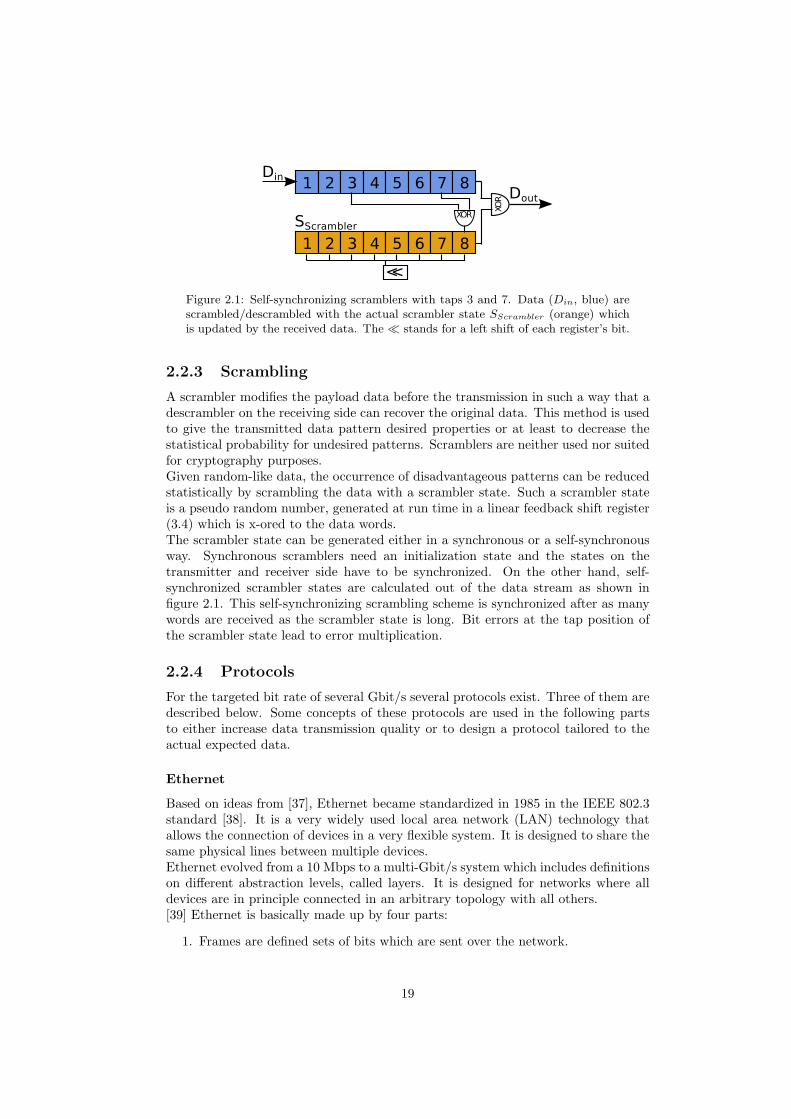
Figure 2.1: Self-synchronizing scramblers with taps 3 and 7. Data (Din, blue) arescrambled/descrambled with the actual scrambler state SScrambler (orange) whichis updated by the received data. The ≪ stands for a left shift of each register’s bit.
2.2.3 Scrambling
A scrambler modifies the payload data before the transmission in such a way that adescrambler on the receiving side can recover the original data. This method is usedto give the transmitted data pattern desired properties or at least to decrease thestatistical probability for undesired patterns. Scramblers are neither used nor suitedfor cryptography purposes.Given random-like data, the occurrence of disadvantageous patterns can be reducedstatistically by scrambling the data with a scrambler state. Such a scrambler stateis a pseudo random number, generated at run time in a linear feedback shift register(3.4) which is x-ored to the data words.The scrambler state can be generated either in a synchronous or a self-synchronousway. Synchronous scramblers need an initialization state and the states on thetransmitter and receiver side have to be synchronized. On the other hand, self-synchronized scrambler states are calculated out of the data stream as shown infigure 2.1. This self-synchronizing scrambling scheme is synchronized after as manywords are received as the scrambler state is long. Bit errors at the tap position ofthe scrambler state lead to error multiplication.
2.2.4 Protocols
For the targeted bit rate of several Gbit/s several protocols exist. Three of them aredescribed below. Some concepts of these protocols are used in the following partsto either increase data transmission quality or to design a protocol tailored to theactual expected data.
Ethernet
Based on ideas from [37], Ethernet became standardized in 1985 in the IEEE 802.3standard [38]. It is a very widely used local area network (LAN) technology thatallows the connection of devices in a very flexible system. It is designed to share thesame physical lines between multiple devices.Ethernet evolved from a 10 Mbps to a multi-Gbit/s system which includes definitionson different abstraction levels, called layers. It is designed for networks where alldevices are in principle connected in an arbitrary topology with all others.[39] Ethernet is basically made up by four parts:
1. Frames are defined sets of bits which are sent over the network.
19

2. A media access control protocol manages the fair access to channels which areshared between multiple devices.
3. The component which physically sends the data.
4. A physical medium is used to carry the digital signals.
In order to be able to use the same physical layer to send information from onepoint to another, the above-mentioned frame structure is introduced. An Ethernetframe consists of a preamble, the destination address, as well as the source address.This information is used by all attached devices to identify frames destined for them.This header is followed by information about the frame size, the actual data and acyclic redundancy check (CRC) hash as described in section 2.3.3.Modern Ethernet networks operate with duplex lines which are rarely used by mul-tiple devices. All devices are usually connected to a switch that handles potentialcollisions, which would occur if different devices access the same lane at the sametime [39]. Even though Ethernet is designed for communication in LAN, whereat least in principle multiple devices access the same lines, useful concepts can beextracted also regarding point to point connections.
10GBASE
Different higher level protocols describe how the above described Ethernet framesare transmitted in detail. A subgroup of such specifications is built by the 10GEtechnologies which specified an explicit duplex 10 Gbit/s transmission. Differentversions for copper and optical physical layers exists. Here, the focus is on theoptical versions as described in the IEEE standard 802.3ae [40]. Different physicalspecifications exist for different distances of data transmission. The focus is againon the short range version 10GBASE-SR that is specified to use 850 nm lasers,optical multi-mode (OM2) fibers, which have a maximal range of 50 meters, 64b/66bencoding as described in section 2.2.2 and specified in [41], and that is designed fora data rate of 10.3125 Gbit/s.The available optical SFP hardware, as described later on in section 5.1.3, fulfills thisspecification and a 10GBASE PCS can be implemented very easily into the StratixV FPGA IP hard cores (see 5.1.1). Nevertheless, it should be noted that whis wouldfix the data rate at 10 Gbit/s.
Interlaken
Contrary to the Ethernet protocol described above, the Interlaken protocol specifiesa chip-to-chip interface for networking. This rather new protocol is designed as asuccessor of the XAUI [42] and SPI4.2 [43] protocols. The purpose of this shortoutline is to identify ideas which could reasonably also be used for a specificallydesigned protocol for the Mu3e data readout. Therefore, only the new Interlakenprotocol is presented and not the two underlying older protocols.Interlaken is designed to operate on multiple lines in parallel and its performancescales with that number. Nevertheless, it can also be operated with only one line.Interlaken uses 64 bit input data to generate 67 bit patterns. A 64b/66b encodingwith additional running disparity control is applied and the generated data patternsare fed through a scrambler as described in section 2.2.3.In the following the different Interlaken concepts are described in detail. The focusis on properties that are also important in single lane operation mode.
20

Figure 2.2: Interlaken protocol overview. The framed data is divided into differentbursts. These bursts are sent within a meta frame on single lines.
In general, Interlaken communications are wrapped in frames. They are used forsynchronization of the different parts and to share diagnostic information betweenthe two devices. A frame’s data is splitted into bursts, a package of data transmittedserial on one single line. The per lane communication is wrapped into meta frames.Figure 2.2 shows the different data wrappings.
Meta Frames Meta frames are used for synchronization and diagnostic purposes.An Interlaken meta frame consists of a synchronization part, the scrambler state,optional skip words for phase compensations, the payload, and some diagnostic atthe end. The synchronization is implemented by sending the control word type“b011110” and the alignment pattern “h0F678F678F678F6”. The skip words arededicated words, which do not contain any data and therefore are skipped at thereceiver side, which introduces a certain capability of rate matching. The type isspecified by “b000111” and contains the fixed pattern of “h21E” followed by sixtimes “h1E”.The diagnostic type is specified by the pattern “b011001” and contains mainly aCRC32 (see 2.3.3) hash over the whole frame where the three highest bits are neverincluded and the scrambler state is set to all zeros for hash calculations because itcan be different for each lane. The used CRC32 polynomial is given by
x32+x28+x27+x26+x25+x23+x22+x19+x18+x14+x13+x11+x10+x9+x8+x6+1(2.3)
Burst and Frames Interlaken distinguishes between bursts, which are associatedto single channels and bound by two control words, and frames which can includemultiple bursts and contain a package of data as described above.The data package is sent over one or multiple channels in bursts whose length isvariable, but limited by an upper and lower limit. Between two bursts, there isalways a burst control word whose bits 65 to 64 are set, according to 64b/66bencoding (see 2.2.2), to “01” and the next lower bit 63 to “1”. Table 2.3 shows howburst/idle words are built exactly.
The lower limit of the burst length can introduce data words which cannot beused. To avoid this, dedicated algorithms are described in the specification to findthe optimal burst length given the allowed burst length range [44, p. 16].
Control Words As described in section 2.2.2 about 64b/66b encoding and insection 2.2.2 about running disparity, the first three bits are used for disparity controland to indicate control words. If a control word is detected, bit 63 indicates whetherit is a burst or a framing control word. In the case of a burst control word, the next
21

Bit66 Inversion65:54 framing “10”53 Control “1”62 Type61 start of packet (SOP)60:57 EOP Format56: Reset Calendar55:40 In-Band Flow Control39:32 Channel Number31:2423:0 CRC24
Table 2.3: Structure of an Interlaken idle/burst word [44].
bit, number 62, indicates whether it is a burst control word with a following start ofpacket (SOP) flag or an idle statement to fill up unused data slots. Table 2.3 showsa control word overview.If the current data is a burst control word, the end of packet is indicated in thebits 60 to 57 with a leading “1”. The following bits state how many data words,consisting of 8 bits, of the current word in the bits 55 to 0 are valid and still belongto the ending packet. The pattern “0000” in these dedicated bits indicates that thecontrol word is not an end of package word and the pattern “0001” indicates theoccurrence of an error in combination with the end of the package.The last 24 bits of a burst control word contain a CRC24 hash of the previous databurst and the current control word. (see 2.3.3). The CRC24 is calculated with thefollowing polynomial: [44, p. 18]
x24 + x21 + x20 + x17 + x15 + x11 + x9 + x8 + x6 + x5 + x+ 1 (2.4)
Synchronization The Interlaken specification explains exactly how the synchro-nization of each lane as well as multiple lines with respect to each other have to besynchronized. The single lanes synchronize to the clock data recovery (CDR) (seeA.1.1), to the 64b/67b word boundaries and the scrambler state. The interface as awhole first synchronizes all single lanes and then aligns the lanes in addition.
Flow Control The protocol leaves open whether the flow control, a status aboutall used lanes, is incorporated into the data stream or whether an off flow solutionis chosen. Once a channel is open, the transmitter is allowed to use it. No creditsystem is implemented. The in-band flow control is encoded into the burst and idlecontrol words.
Scrambler In contrast to the 58 bit long scrambler, which is self-synchronizedon the payload in the older Ethernet IEEE 802.3 [38] standard, Interlaken uses anindependent synchronous scrambler for each line. This mainly reduces the dangerof error multiplications (see 2.2.3). The scrambler state is payload independent andgenerated out of the taps 58 and 39. The downside of this scheme is the needfor scrambler state synchronization, which is the reason why the scrambler state istransmitted in the meta frame header. The control word type, which contains the
22

58 bit of the scrambler state is indicated with the type “b001010”. The scrambler isnever applied to the three highest bits which contain the parity and the type pattern[44, p. 30].
2.3 Signal Quality Check
Once the physical and digital encoding of data described in section 2.2 are imple-mented, online signal quality checks are a desired feature. In the first two subsectionsof this chapter, tools for physical signal quality checks such as eye diagrams and bath-tub plots are described. In a second step, cyclic redundancy checks are introducedwhich allow an evaluation of the correct data transmissions by adding only a verysmall amount of extra data.
2.3.1 Eye Diagrams
Eye diagrams are a tool to screen the signal quality in fast data transmissions wherenon-return-to-zero (see 2.2.1) schemes are used. The different transitions from a“1”-state to a “0”-state and vice versa are folded into a single diagram. Perfectsignals, where the transitions are performed instantaneously result in a square withthe length Tbit = 1
f where f is the serial clock frequency of the data transmissionand the height Vdiff is the differential voltage.The physical medium which propagates the signal as well as all included electroniccircuits constitute a low pass filter and deform the signal. The folding of real signalslooks much more like an eye. Figure 2.3 shows an example eye diagram. Thepresented signal shows a wide eye opening, very little jitter, a crossing level almostin the center and much faster falling times than rising times.
Jitter introduced either by the transmitter and receiver units or the clock re-covery circuits (see A.1.1) result in misalignment of the data transition lines in thehorizontal time axis. The eye width is an indicator how well the clock recovery isworking. The eye height is the difference between the lower limit of the one-level andthe upper limit of the zero-level inside the eye. Only if the eye is open enough, whichmeans that both height and width cannot be too small, a secure recovery of the sentbits is possible. A further indicator is the level at which the falling and rising edgescross. Distortions in the clock cycle or signal symmetry problems manifest in a cross-ing level that is not located exactly in the middle between the one- and zero-level [45].
2.3.2 Bathtub Diagrams
Similar to the eye diagrams extracted from the pure signals, one can add a bit errorrate test (BERT) (see 5.2.2). So-called bathtub plots can be produced by measuringthe bit error rate (BER) for different values of the signal height thresholds or byadding an offset to the recovered clocks signal. Examples of such plots are shownin the lower part of figure 2.4. They show the clock offset and the signal thresholdversus bit error rates. The desired eye opening for a targeted BER can be estimatedwith these plots. If the two variables clock offset and signal height threshold arevaried simultaneously, 3d plots with clock offset, and signal threshold versus biterror rate can be extracted. 2d projected contour plots look very similar to the eyediagrams described above, although they are not exactly the same [46, 47].
23

Figure 2.3: A typical eye diagram with indicated width, height, jitter and crossinglevel. This particular signal shows a much faster falling than rising time.
Figure 2.4: BER bathtub plots. The upper two plots show the projected 3d plots,where the lower two plots show the 2d projections which results in bathtub plots.
24

Even though the EyeQ circuits described in A.1.1 are called eyes, they representmore the second type of eye diagrams where a BER measurement is required.
2.3.3 Cyclic Redundancy Checks (CRC)
A cyclic redundancy check (CRC) is used for error detection in data transmissionsor storage. It is a checksum with a set of very convenient properties, but it is not acryptographic hash. CRC is essentially the remainder of a polynomial division whichcan be implemented very efficiently in hardware.
CRC as a Polynomial Division
Given data, represented in binary form, can be understood as a polynomial of thefollowing form
a(x) = a0xl−1 + a1x
l−2 + ...+ al−2x+ al−1 (2.5)
where an ∈ F2 = 0, 1 are the bits of the given data and therefore a(x) ∈ F2[x].The polynomial division of a polynomial p(x) by another polynomial q(x) can beexpressed as finding s(x) so that there is r(x) a reminder polynomial with degreeless than q(x):
p(x) = s(x) · q(x) + r(x) (2.6)
The finite set of all possible r(x) describes all possible CRC values given a fixeddivider q(x) = pCRC(x). For technical reasons, the polynomial is defined after amultiplication with xN
a(x) · cN = b(x) · pCRC(x) + rold(x) (2.7)
where N is the length of the CRC polynomial. Note that one is not interested inhow b(x) looks like [48, p. 3].
The above described polynomial division can be implemented with a register ofthe width N where the data bits are shifted in series. As soon as the bit shifted outof the other end is different from the current input bit, the register content is xoredwith the fixed CRC polynomial. Usually the register is filled with all ones to start.Alternative to this bit wise calculation, the CRC can be calculated out of tableswhere up to eight bits can be treated reasonably at the same time. Table 2.4 showsan example how a 4 bit CRC hash is calculated out of an 8 bit word.
10011011 000⊕ 1011
00101011 000⊕ 1011
00000111 000⊕ 101 1
00000010 100⊕ 10 11
00000000 010
Table 2.4: CRC example. The CRC of the input data “10011011” is calculated witha CRC polynomial x3 + x1 + 1, which corresponds to “1011”. The resulting CRChash is “010”. ⊕ stands for xor.
25

Online CRC Error Check
If the calculated CRC is added to the data out of which it is calculated and the CRCis evaluated again including the appended code, the CRC is always 0. Adding therold(x) obtained from 2.7 to the data a(x) to get the new data a′(x) can be writtenas shifting a(x) N bits and then add rold(x), hence
a′(x) · xN =(
a(x) · xN + rold(x))
· xN (2.8)
= (b(x) · pCRC(x) + rold(x) + rold(x)) · xN (2.9)
= b(x) · xN · pCRC(x) + 0 (2.10)
the last step is true because p(x) = −p(x) since the polynomials p(x) ∈ F2[x]. As itcan be seen in equation 2.10 rnew(x) = 0 [48, p. 8].
Error Detection Strength
The error detection strength of a CRC code depends very strongly on the usedpolynomial. In general
• All single bit errors are detected by polynomials with order of at least two.
• All two bit errors are detected if the CRC polynomial does not divide the termxi(1 + xj−i) for i > j
• All odd numbers of errors will be detected if the polynomial is a multiple ofx+ 1.
• Burst errors of the length b, continuous patterns of the length b where the firstand last bits are errors and the state of the bits in between are unknown, aredetected of polynomials by the length b or longer and with a x0 term [49].
There are many of standard CRC polynomials which are widely used although theremay very often exist better choices. Particularly because the CRC error detectionstrength depends strongly on the used data width, a careful and application suitedpolynomial choice makes very often sense. In [50] and [51], a variety of polynomialsis presented, and their performance with different data sizes performance is shown.
26

Chapter 3
Electronic Components
In this chapter, different electronic elements, which are referred to at various parts ofthis work, are explained in detail. This chapter’s intention is to provide a reference.
3.1 Logic Gates
Logic gates are electronic circuits implementing Boolean functions. They build thesmallest logic element of a digital circuit and are usually implemented by transistors.Table 3.1 shows the different types with the associated symbols.
AND OR NOT
Table 3.1: Simplest logic gates with their symbols.
In addition to these Boolean function gates, tree-state gates allow the removal ofan output from a circuit by a high impedance state. The same output can be sharedby multiple circuits.
3.2 Memory Elements
The capability to store, respectively buffer, electric signals is a main ingredient formodern sophisticated electronics. Beside the naive and very simple approach ofstoring signals in long cables, different elements have been developed in the past.Particularly in clocked logic circuits they simplify the timing.
3.2.1 Flip-Flops
A flip-flop is used to store information in an electrical circuit. A flip-flop circuit hastwo stable states between which can be switched by applying a signal to a dedicatedport. The simplest possible flip-flop, an SR latch, is shown in figure 3.1 where S isthe signal, R a reset and Q and Q the signal, respectively the inverted signal [52].
27

Figure 3.1: RS latch flip-flop.
3.2.2 Random-Access Memory (RAM)
This kind of storage devices provide addressed storage. That means, that throughan address bus every memory cell can be read and written at any time. This featureis called random-access. When the device is not powered, the data is lost - RAMis volatile. It can be distinguished between static (SRAM) and dynamic (DRAM),where the first must not be refreshed periodically.
3.2.3 First In First Out (FIFO)
A FIFO is a memory unit which outputs the data which are put in at first, again atfirst. The name is an acronym for First In First Out. In electronics the storage can beimplemented in various ways such as SRAM, flip-flops or others. It is distinguishedbetween FIFOs with a common clock for read and write and FIFOs with two differentclocks for the write and read process. Furthermore, FIFOs consisting of more thana few words, very often have a full and an empty port to indicate these two stateswhich may cause errors.
3.2.4 Read-Only Memory ROM
In the contrary to RAM, read-only memory cannot be written to. This memory isused to store small programs, constants or look-up tables of mathematical functions.In 1956 programmable (PROM) memory was introduced, which cannot be writtenat run time but programmed before. This offers new flexibility [53].
3.3 Phase Locked Loop (PLL)
A phase locked loop (PLL) is a highly non linear circuit that outputs a signal whosephase is correlated to the input signal. There are many difference types of PLLsnevertheless the underling concept shown in figure 3.2 is always the same. A phasedetector (PD) compares the phase different between the input signal Sin, which canbe understood as a reference signal, and the feedback signal Sfb. The PD signal Sp
is fed through a filter, in most cases a low pass filter (LPF), and is then used tocontrol a variable frequency oscillator (VFO) whose signal is then looped back tothe PD and serves as an output Sout. If all the components are properly tuned, thesystem locks itself in a stable condition [54, p. 4f].
In FPGAs cascading PLLs can be used to generate clocks with significantly differ-ent frequencies than those available from external oscillators. They are also heavilyused in clock recovery circuits. In general, there can be three different types of
28

Figure 3.2: Block diagram of the basic PLL concept.
PLLs inside an FPGA. Clock Multiplier Unit (CMU) PLLs add one divider into thefeedback loop (M) and one into to input signal (N) to achieve locked output signalswith a multiplicity of the input frequency. Fractional PLLs (fPLL) add an additionaldelta sigma modulation into the feedback loop, which allows fractional values [55].Altera has introduced auxiliary transmit (ATX) PLLs, which have the same buildingblocks as CMU PLLs, but are tuned for low jitter at high frequencies [56, p. 1-13].
3.3.1 Clock Data Recovery (CDR)
In serial data transmissions, the underlying clock is very often omitted. PLLs fed bythe serial received data stream lock to data base frequency. This clock data recovery(CDR) is crucial for successful data transmission and requires enough transitions inthe data stream.
3.4 Linear Feedback Shift Register (LFSR)
A shift register consists of a series of flipflops (see 3.2.1) with the same clock andwhose output is fed into the next flipflops‘ input. The input bit of a shift registeris only the one foremost bit [57]. In most general notation, a linear feedback shiftregister is a shift register whose input bit is a linear combination of its previous state.
3.4.1 Pseudo Random Number Generators (PRN)
For well suited linear functions, pseudo random periods with maximal cycle lengthsof 2n−1 ,where n is the number of bits in the shift register, can be achieved. In sucha scheme, the bits at different positions, called taps, are xored to obtain the inputbit. Very often, this is expressed in a polynomial in F2[x] as shown in equation 3.1for an 8 bit PRN. Where the exponents indicate the used taps and the 1 = x0 theinsertion position of the new bit.
x8 + x6 + x5 + x4 + 1 (3.1)
For many different PRN lengths schemes with two or four taps exist. For maximallength PRN the number of taps has to be even, and all used taps must not shareany conmen divisor except for 1. Useful taps for LFSR up to 786 can be found forexample in [58].
3.4.2 Counter
LFSR can also be used as counter. Because of their relative simple feedback logicwith only a few xor gates they can be operated very fast. Counters based on LFSR
29

are faster than Gray counters (see 3.5), but the advantage of only one bit flip is lost[59].
3.4.3 Other Uses
Linear feedback shift registers are also used to generate test patterns for data trans-mission (see 5.2.2) and used for data scrambling (see 2.2.3). They are not suited forany cryptographic use.
3.5 Gray Counter
A binary Gray code of order n is a list of all 2n n-bit strings such thatexactly one bit changes from one string to the next [60, p. 32].
Hence, Gray codes are used for error minimizing in analog to digital encoding andto avoid errors due to readouts during flipping states. They are particularly usefulbetween two clock domains. Gray code counters are very often used for fast countersin electronic devices.
Example The easiest way to convert binary to Gray and vice versa are explainedbelow in 1 and 2. The here shown implementation of a Gray code is also calledreflected binary code. Less demonstrative, but more efficient, decoding schemesexist.
Algorithm 1 Binary to Gray Code Conversion
outgray ← (inbin ≪ 1)⊕ inbin
Algorithm 2 Gray Code to Binary Conversion
num← ingray
mask ← ingray ≫ 1for mask 6= 0 do
mask ← mask ≫ 1num← num⊕mask
end foroutbin ← num
30

Chapter 4
Field Programmable LogicGates (FPGA)
Field-Programmable Gate Arrays (FPGA) were developed in the late 1980s in an en-vironment where electronic systems were mainly composed of standard components,such as microprocessors, memory chips or logic components, mounted directly ontomulti-layer printed circuit boards (PCBs). The rapid increase of complexity in thesesystems led to much higher possibility of incorrectly connected components on suchboards.Programmable interconnections between components offer the possibility to test de-signs before production and introduce the new opportunity to adapt the functionalityof components during operation to fulfill new requirements. In principle every inputand output (I/O) pad can be connected to every logic component on the board.This programmability feature introduces an increase of latency between the singleelements, which significantly reduces the maximum speed at which the devices canbe operated.
The idea of adjusting the hardware to a given task is best met in application-specific integrated circuits (ASICs). They are commonly used and are known tooperate most cost effective for large production numbers, fastest and with lowestenergy dissipation [61, p. 1.1]. Nevertheless, the re-programmable properties ofFPGAs overcome the run-time advantages of ASICs in many cases [61].
As shown in figure 4.1, FPGAs consist of arrays of logic blocks. These blocks canbe simple transistors as well as much more complicated structures such as memoryblocks, phase locked loops (PLLs ct. 3.3.1), or even a microprocessor. In modernFPGAs, most of the blocks are pairs or quartets of transistors, small gates, mul-tiplexers, look-up tables or different AND-OR structures. The Interconnection ofthese blocks is programmed by electrical switches, which can be implemented withdifferent technologies such as SRAM, EPROM or Antifuse [62].
Modern FPGAs are produced in the same technology also used for other microprocessors. Various intellectual property (IP) hard cores are embedded inside thechips to fulfill highest performance and in some cases security requirements. Figure5.1 shows a modern FPGA from Altera which includes many IP hard cores mainlywith the aim to achieve the highest possible bandwidths with the ultimate flexibility.Particularly the use of IP hard core transceivers allows significantly faster data rates.Rates that could never be achieved by the, in relation, slow FPGA logic gate arrays.
31

Figure 4.1: FPGA architecture: logic blocks in green, I/O pads in orange andprogrammable interconnections in blue.
32

Part III
Measurements
33

Chapter 5
Optical Links
5.1 Soft- and Hardware
The used soft- and hardware are assembled around Altera Stratix FPGAs devel-opment kit which build the core of every setup. Therefore, the used FPGAs aredescribed in detail. In the following part, daughter boards and smaller componentssuch as plugs and cables are described.
5.1.1 Altera Stratix V Development Kit
In all used setups, DSP version Stratix V GS Development Boards are used. Figure5.2 shows such a board with the embedded inputs and outputs to evaluate variousdata transmission possibilities [63, 64]. The core component is a Stratix V FPGA.
Stratix V FPGA
The Stratix V from Altera is produced in a 28 nm structure size process. As shownin table 5.1 and the scheme in figure 5.1 many intellectual property (IP) hard coresdesigned for signal transmission, especially high bandwidth transceivers, are avail-able.
In the following, selected components of the FPGA are explained.
Adaptive Logic Modules (ALM) Linked ALMs are used to implement anydesired logic functions in the FPGA and make up by far the biggest part. TheStratix V FPGA has of 262400 adaptive logic modules (ALMs) which consist of 8inputs, a look-up table (LU), two adders, as well as four registers [65].
ALM 262400DSP blocks (18x18) 3926M20K 2567PCIe IP blocks 2Transceivers 48 (up to 14.1 Gbit/s)
Table 5.1: Stratix V (5SGSMD5K2F40C2N) specifications.
34

Figure 5.1: Altera Stratix V architecture [63].
Digital Signal Processing (DSP) Digital Signal Processing (DSP) blocks con-tain hard cores, spacial purpose logic circuits. The Stratix V device offers a hugevariety of such cores ranging from encryption, video and audio handling, differentsignal modulators, fast Fourier transformations, hashing up to floating point additionand multiplication cores. Stratix V allows DSP blocks with configurable precision[66, 67].
Embedded Memory (M20K) Stratix V devices have embedded MLAB as wellas M20K memory blocks inside the device which both can be accessed with up to 600MHz. The MLAB is a general-purpose dual-port memory array of 640 bits optimizedfor FIFOs and shift registers for DSPs. M20K blocks are dedicated memory blockswhich are much larger (20 Kbit) [68].
Stratix V Development Board
The different components of the Stratix V development board, shown in figure 5.2,are explained in the following.
SubMiniature version A connectors (SMA) SubMiniature version A (SMA)connectors are differential coaxial radio frequency connector pairs designed for fre-quencies up to 18 GHz with an internal 50 Ω impedance. On the board they can beused to output electrical high frequency signals. Due to their small distance to thetransceivers inside the FPGA, excellent signal quality is achieved [69].
High Speed Mezzanine Card HSMC The Stratix V development board pro-vides two ports for high-speed mezzanine cards (HSMC). They are designed formulti-gigahertz data transfers and provide up to 192 pins. These standardized portsallow to access the full input and output (I/O) capability of the FPGAs by achieving
35

FPGAPCI Express
HSMC Port A HSMC Port B
40GB QSFP
LCD
SMA
Field-ProgrammableGate Array
High Speed Mezzanine Card
16x2 chars
coaxial
Quad Small Form-
Figure 5.2: Altera Stratix V Development Board [63].
a maximum of flexibility at the same time [70]. Up to 8 multi-Gbit/s lines can beimplemented per port.
Quad Small Form-factor Pluggable (QSFP) Quad Small Form-factor (QSFP)are hot-pluggable interfaces designed for high rate data transmission up to 4x28Gbit/s [71]. The Stratix V development board supports data rates up to 4x10Gbit/s.
PCIe, USB, Ethernat and JTAG The development board provides a backplaneinterface designed for PCIe slots and data transmission. Further communication andreprogramming of the FPGA are provided through an USB, an Ethernet and a JTAGinterface. An USB blaster chip on the board support easy and fast reconfigurationof the device without any other hardware than a regular USB cable. In addition,it is possible to load FPGA programs via Ethernet into the on board flash memoryand restore the setting after power up of the FPGA.
Oscillators The development board includes many programmable base oscillators[72, p. 2-23]. These oscillators are used to generate various clocks. Many of themare not available on the entire FPGA. Very often they can be accessed only withinregions where the designated IP hard cores for usages the clocks are designed forare situated. For example, the 282.5 MHz clock labeled with REFCLK4 QL2 Pgenerated with a Si5388 oscillator and designed for transceivers used in combinationwith the on-board QSFP interface are available only for these transceivers. Thisclock frequency cannot be used as input frequency for transceivers used with theHSMC interface.
Memory Different memory types and sizes are available on the board. A 1152Mbyte DDR3 SDRAM with a 72 bit data bus, 4.5 Mbyte QDRII+ SRAM with a 18
36

bit data bus for writing and reading up to 550 MHz and a 72 Mbyte CIO RLDRAMII with a 18 bit data bus are available. Additional 512 Mbyte flash memory fornon-volatile memory as mentioned already in the JTAG section 5.1.1 can be used.
Stratix V Transceivers
As described in section 5.1.1, the transceivers of the Stratix V FPGA are IP hardcores. This transceiver implementation provides a separation between the very fastserial part and the slower part where the data can be treated in parallel. Hard coresallow much faster rates than possible with logic gate arrays. Serial data rates up tomulti-Gbit/s can thus be realized.
Each transceiver channel consists of a transmitter and a receiver part. Therefore,the channels are called full-duplex. The transmission, as well as the receiver partconsists of a hard core physical media attachment (PMA) and a by-passable physicalcoding sublayer (PCS). The three different PCSs standard, 10G and PCIe Gen3 areavailable for each PMA. A detailed description can be found in section A.1.
5.1.2 SantaLuz Mezzanine Board
The SantaLuz Mezzanine card shown in figure 5.3 has been designed and producedat TU Dortmund. TU Dortmund developed this board in 2011 for a test bench ofa fast data transmission line [73, p. 20]. The card is designed for data rates up to8.5 Gbit/s [74] and it was shown that all eight channels are operational with a BERsmaller than 3 ·10−15 at 6.25 Gbit/s. All used SantaLuz boards are revision 0 boards[75].The mezzanine card is designed for use as a Stratix daughter board attached to theHSMC ports to provide up to eight SFP+ plugs. Therefore, the SantaLuz card isequipped with female HSMC connectors. The SFP+ specification foresees ports toaccess an optional internal memory, this feature is not realized in the SantaLuz card.Although the plugs would allow a direct connection, high speed extension cables areneeded due to the available space.
5.1.3 Plugs
The used Stratix V development boards and mezzanine daughter boards providedifferent types of plugs for data transmission. In the following extensively usedelectrical and optical plugs for SFP and there related QSFP cages are described.
SFP Plugs
Small form-factor pluggable (SFP) is a specification for transceivers developed bythe multiple source agreement (MSA) group [76]. They build an interface to opticalor copper networking cable, where their relative small size allows a high density ofplugs on various devices. In 2006 an enhanced version of the SFP, the SFP+, wasintroduced, which supports data rates up to 10 Gbit/s [77].In the following the different SFP plugs used are explained.
37

Figure 5.3: SantaLuz mezzanine board produced at TU Dortmund.
Figure 5.4: Top and side view of an electrical SFP plug.
Electrical SFP Plugs SFP to SMA adapters (SFP2SMA) from TrioFlex areused to access the fast signals at the SFP plugs electrically (see figure 5.4). Theplugs consist of four PCB layers where the impedance matched high-speed lines ofthe transmitter and receiver channels are length matched. No DC block capacitorsare present [78]. These plugs are mainly used to examine output signals on anoscilloscope.
Figure 5.5: Optical SFP plug overview. AFBR-57D7APZ
Optical SFP Plugs Optical duplex transceivers from Avago for multi-mode op-tical fibers are used in different setups (see figure 5.5). The Avago transceiver worksat different rates with 850 nm wavelengths, where 2.125, 4.25 and 8.5 Gbit/s are
38

ensured by the manufacturer. The rate selection is handled automatically by the de-vice and although the SFP specification would provide rate selection, this is ignored.The transceiver is designed to work in a temperate range between −10C to 85Cwith a supply voltage of 3.3V±10%. Both, the Rx and the Tx lines are AC coupleddifferential lines. The Rx lines need an external 100Ω termination which results ina voltage swing between 370 and 850 mV . The Tx lines are 100Ω terminated insidethe module and accept a differential swing of 180 to 1200 mV .
The 850 nm laser pulses are generated in a vertical cavity surface emitting laser(VCSEL). The incoming differential high-speed logic signal is used to modulate thelaser diode driver current. Provided the incoming data pattern is DC balanced, thetransmitter laser driver circuit regulates the optical power at a constant level. Avagodoes not state over how many bits the signal should be DC balanced, but mention8b/10b encoded (see 2.2.2) data as an example.
The receiver section includes a photodiode, an amplification and a quantizationcircuit.
Beside the basic functionality, the transceiver provides an internal memory whichcan be used to access real time temperature, supply voltage, bias laser current, laseraverage output power and received input power besides the standard SFP data. [79]As mentioned before, the used mezzanine daughter board does not support accessto this transceiver internal memory.
5.1.4 Cables
A variety of different cables were used in different setups. On one hand there arecommercial standard solutions either to connect components or for data transmissionand on the other hand some cables were specially developed.
Commercial Cables in Setups
A HSMC cable from Samtec is used to connect daughter boards to Stratix V develop-ment board. The same type of cable with two female plugs could in principle be usedto connect two development boards. With HSMC Altera developed an own standard,whose specifications are met by the Samtec 0.5 mm pitch Q Strip QSH QTH serieshigh-speed board-to-board connectors. The used 228.5 mm long extension cablesshow a -7dB insertion loss at a frequency of 9.2 GHz [80].
Optical Cables for Data Transmission
As described in section 2.1.2, wave guides can be realized as single or multi-modedevice. Single mode fibers allow the signal to propagate faster and farther than inmulti-mode cables, which are in general much cheaper and easier to use.
Multimode Multi-mode duplex fiber patch cords (FPC) with lucent connectors(LC) on both sides are used in setups with SFP optical transceivers. The so-calledlow smoke zero halogen (LSZH) cable consists of typical fiber coated with a ther-moplastic which does not contain any halogen and produces low smoke if burned.The LSZH feature is purely a safety aspect. This fiber shows an insertion loss below0.14 dB and a return of the order of 37 dB. Cable lengths from 0.5m up to 50m areavailable, where for such multi-mode cables this represents the upper cable lengthlimit at multi-Gbit/s.
39

Single Mode While the optical SFP transceivers are designed and operated withmulti-mode optical fibers, the QSFP transceivers are mounted together with eightsingle mode fibers to one setup. Beside the QSFP plugs, no more connectors areneeded, the fibers are directly glued on the lasers respectively photodiodes [81].According to Molex, the used setups are designed to operate with BER below 10−18
per link in a range from 5 up to 10 Gbit/s. Due to the QSFP mechanical designwith a cage, the devices are hot-pluggable. In addition, the setup with two QSFPuses only 0.78W per active cable [82].As it can be seen from the facts stated above, these cable-plug systems are designedto work out of the box. Usually they are used in telecommunication applications.Point to point connections between devices, such as switches, servers, etc., with avery high bandwidth can be realized very easily up to several kilometers.
5.2 Firmware
Beside the physical hardware, the firmware with which FPGAs are loaded is a verycrucial part of any actual setup including FPGAs. Therefore, the main conceptsof the firmware developed are described in this chapter. In a first section the wayhow transmitter and receiver logic are synchronized is described, followed by anoutline how a user bit error rate test (BERT) is implemented. In a third section, thefirmware required by the Altera transceiver toolkit (ct. 5.2.3) and its possibilitiesare described.
The development of suitable FPGA firmware for link verification tests is a firstpart of this thesis. It will be followed by the performed measurements.
5.2.1 Data Transmission State Machine
Finite state machine (FSM) is a mathematical concept to design sequential logiccircuits. A FSM maps through a transition function all states of a finite inputalphabet depending on a set of finite internal states to an output function out ofa finite set of an output alphabet [83, p. 11f.]. The machine is always in exactlyone state, a transition to any other state is triggered by specified conditions. In themajority of cases, state machines are run synchronously, which means that a clockis present and both the check of the transition conditions and the transitions itselfare performed at every cycle.In the following the concept of the state machine which manages the data receptionis outlined and illustrated in figure 5.6.
In- and Output The state machine gets the received deserialized data from thePMA together with the recovered clock as inputs. The output is composed of thebit error number from the BERT test, the total number of received words and thenumber of synchronization losses. Additional debug information, for example thelast word patterns with errors are provided. Optionally, a flag for a bit slip in thePMA can be output.
Not Sync State The reset puts the state machine into this state. The input datais checked against a specified word alignment pattern (WAP).
40

Figure 5.6: Transceiver state machine with the three different states: not sync(orange), sync (blue) and receiving (green). The conditions for the transitions 1 to5 are adjusted to the needs of the current setup.
Transition 1) If the WAP is not found 400 (bitSlipNo) times one bit is slippedin the incoming data. This can be realized either with the bit slip function of thetransceiver in the PMA or inside the receiving state machine through an additionalregister.
Transition 2) If the WAP is identified 300 (wapNo) times the state machine isset into the synchronized state.
Sync State In the synchronized state the input data is checked against WAPagain. As long as this pattern is detected, the local state machine is synchronous tothe data stream, but no valid data is sent by the transmitter.
Transition 3) In principle it is possible to loose the synchronization in the syncstate and return to the non-synchronized state. A realization of this transitionrequires the ability to detect errors in the WAP pattern and distinguish it from validdata. Without any further protocol, this transition cannot be realized.
Transition 4) Whenever a data word different from the WAP is detected, it isassumed to be a valid data word. Hence, the state machine is put into its receivingstate.
Receiving State In the receiving state any action with the data can be performed.In this setup, a bit error test is performed as described in section 5.2.2.
Transition 5) Based on the results of the BERT, different criteria lead to a lossof synchronization.
• More than a quarter (errRatio) bits of a word contains errors
• More than 256 (erWordNo) words with errors occur in a row
• More than a fixed numbers of errors have occurred. This condition is not usedfor BERT runs and exists only for debug purpose.
41

5.2.2 Bit Error Rate Tests (BERT)
The bit error rate is the number of received bits which are different than they weretransmitted normalized to the total amount of received number of bits. This ratecan be seen as the probability that a single bit state flips.To perform such tests, data in a known pattern has to be sent on the transmitterside. To actually test for bit errors, the expected data pattern has to be known. Thenumber of bits for which expected value and their actual received state differ canthen be counted.The crucial part is how the bit error test gets the information on how the receiveddata pattern is supposed to look like. In the implemented versions, the same datagenerator is used on both transmitter and receiver sides, generating the next patternbased on the previous word.
Data Generator
The data generators implemented need the previous data pattern as input and cal-culate the new pattern. Various different patterns are used for testing purpose. Thesimplest pattern are fixed patterns, which do not depend on the previous words.They are used to establish a new connection, in this case word alignment patterns(WAP) are generated, or to test special patterns. By sending a fixed numbers ofzeros followed by alternating one and zero patterns, the zero acceptance of a systemcan be tested.
A counter can be easily implemented to generate a deterministic pattern. Thisallows latency measurements of the system. It has to be mentioned that bit patternrepresenting numbers can contain a lot of zeros, a quite disadvantageous pattern.To avoid this disadvantage one can start the counter at a value where less zeros ina row occur or use gray counters. The problem however cannot be avoided in thelong run.
Most of the time pseudo random number (PRN) generators (see 3.4.1) with pe-riodicity maximizing taps are used. The length of the PRN determines the numberof different possible states, the actual generated words can be of arbitrary length.
Test Pattern Quality
Pseudo random number generators, which generate the new bit state out of a 31bit state, are commonly used for signal integrity tests. These pattern generators areoften called PRBS31. Assuming an 8.0 Gbit/s data transmission with a PMA widthof 80 bits, as it is used in the measurements with tuned transceivers in section 5.3.4,all of the 231 = 2.1 · 109 possible words are transmitted once in 0.27 seconds. Thesingle transmission of each possible state of this data is not enough to measure realbit error rates. To test also for random jitter and sinusoidal jitter, all patterns haveto be transmitted many times because these effects behave independently of the bitpattern. Ransom Stephens stated in [84] that each pattern should be sent at least 20times. If bit error rates are measured down to < 10−16, each pattern is transmittedover 59’000 times. This is certainly enough to tests for all combinations of patternand any kind of noise respectively jitter with reasonable statistics.
42

BERT Implementation
Figure 5.7 shows the implementation of the bit error test described above into theFPGA logic. The received data from the last cycle is sent to an instance of the
Figure 5.7: Simplified flow diagram of bit error rate test (BERT) with the mostimportant counter Nerr.
same data generator, which generated the data on the transmitter side, to get thesupposed data pattern. The received data is compared to the expected pattern.If the two patterns show any difference, their differing bits are stored in a registerover which is summed in the following cycles. This process is quite timing criticaland therefore split over multiple clock cycles. Once the result is calculated, thenumber of error bits is added to the overall error counter.The expected pattern obtained from the data generator does not match the realpattern if the input pattern already contained an error. Hence, if only one errorcontaining word occurs, it is counted twice. If a series of words contains errors,one word is counted too much. This problem is addressed by counting the errorcontaining words in a row and always correct for the last one. Therefore, if thegenerated and received pattern match, but an error was indicated in the last word,this error was introduced artificially and has to be corrected for in the overall errorcounter. This procedure allows the error counter to display a too large value only
43

for a couple of clock cycles. Too low values cannot occur.
5.2.3 Altera Receiver Toolkit
As described in section A.2 the Altera Quartus II software development kit (SDK)provides different useful programs for optimization of the logic designed. The AlteraTransceiver Toolkit provides a GUI for dynamic reconfiguration of the transceiverson the FPGA. If the corresponding logic blocks are implemented in the user logic,an access via the system console interface is possible.The Toolkit can be loaded with the same design as it is implemented in the FPGA.All physical transmitters and receivers are then auto detected by the software andcan be controlled individually. To test channels, the individual transmitters andreceivers can be grouped to a data link and then be controlled as data link.To access the functionality of the transceiver toolkit, a special firmware with theabove described logic elements is used.
BERT Swap
The toolkit provides the possibility for a scan over different analog tuning settings.A BERT swap varies all analog parameters (see 5.1.1) inside specified ranges andperforms bit error rate tests during a given time interval. This tool allows to finda suitable range for the analog tune values of a given setup. This tuning method isbased on bit error rates, hence it needs a lot of time to improve the tuning of alreadywell tuned systems.
Manual Eye Tuning
It is not possible to access the eye diagrams (see 2.3.1) of optical signals with theavailable hardware. To find on one hand a suitable range for the automatic tun-ing with the toolkit and on the other hand to understand the available transceiverparameters better, a manual tuning with an electrical signal was performed. TheSantaLuz mezzanine card on the HSMA port equipped with an electrical SFP withthe firmware described in 5.3.4 operating at 8.0 Gbit/s was connected to a digital se-rial analyzer from Tektronix to visually inspect the eye diagrams. Figures 5.8 showsa selection of eye diagrams with the corresponding tune values.
44

(a) un-tuned eye
(b) bad tuned eye: Vod = 25, 2ndpost = −10
(c) well tuned eye: Vod = 26, 1stpost = 11, 2ndpost =1, pre = −2
Figure 5.8: Eye diagrams with different analog tuned transmitter routed over theSantaLuz mezzanine card and an electrical SFP plug.
For an electrical 8.0 Gbit/s setup with the SFP plugs on the mezzanine card, thesettings Vod = 26, 1stpost = 11, 2ndpost = 1, pre = −2 work the best. The optimaltune values for an optical setup are different and stated in 5.1.3 in the measurementchapter.
45

EyeQ Measurements
Figure 5.9: Example of a EyeQ diagram in the Altera Transceiver Toolkit. Thedifferent colored lines stay for different BER levels. The shown eye has an openingof 19/36 for BER of 10−12. The horizontal time axis is divided into 32 units andthe vertical threshold axis into 128 units.
In the Stratix V FPGA used, circuits denoted as EyeQ are available as IP hardcores. These units described in A.1.1 are accessed by the Altera Transceiver Toolkitto sample for an eye diagram. It is important to mention that eyes in this setupare not exactly eye diagrams as mentioned in 2.3.1 but are rather bathtub diagrams(see 2.3.2). The BER is tested at different points in the plane spanned by an offsetin the CRC recovered clock and different thresholds for detecting a zero or a onerespectively. In the eye figure, isolines with the same BER are drawn. These contoursindicate the eye opening for this specific BER.If such EyeQ diagrams are calculated for different runs in an analog tuning scan, theeye opening of the EyeQ diagrams can be used to find the best suited analog tunevalues. Figure 5.9 shows an example of such an EyeQ diagram. It is to be mentionedthat the circuits only provide eyes down to BER of the order of 10−12. This is dueto the fact that more precise measurements would need too much time and limitsthe exact tuning if much smaller BER are aimed for.
5.3 Measurements
This chapter describes all performed measurements with their corresponding setupsusing the hardware described in chapter 5.1 and firmware based on ideas which aredescribed in chapter 5.2. Various bit error rate tests (BERTs) have been performedto test the high speed optical links of the MuPix readout chain. In a first part,the statistical approach used for measurements without any error is introduced.Followed by single and multi-channel measurements with optical SFP links. In afourth chapter, measurement with optical QSFP links are presented.
5.3.1 BER Upper Limit and Error Calculations
The performed measurements of BER are classical counting experiments. There aretwo ways to understand these measurements. On one hand, one can consider N
46

binary measurements which check whether a bit error occurs or not. The sum oferrors is denoted k and the probability of a single bit to be an error is p. The twoquantities k and N are actually measured. The best estimator for p is then p = k
N .The variance of such a measurement is given by
V arbinom[X] = Np(1− p) = k(1− k
N) (5.1)
for large N and relative small k the binomial distribution converges to a Poissondistribution and the variance is approximated by k.On the other hand, one can consider that one single measurement of the quantityk = p · N is performed and assume that the rare process of bit errors is Poissondistributed. In this case the parameter s of the distribution described in 5.5 is givenby s = E[X] = k. The variance can be written as
V arPois[X] = s = s = k = p ·N (5.2)
where p is the best estimator for p.In both perspectives described above, the best estimator for BER p, with its erroris given by:
BER = p =k
N±√k
N(5.3)
Where the stated error is valid for Poisson distributions or if p is small. BERs arehere considered small.
According to [85] there is no standard prescription for setting upper limits forrare signals. In a Bayesian approach the probability density function (pdf) of aunknown parameter is given by equation 5.4
π(s|n) = f(n|s)| · π(s)∫
∞
0f(n|s)π(s)ds (5.4)
where s is the given signal rate, n the number of observed events, f(n|s) the con-ditional probability to observe n events by given signal rate s and π(s) is the priorpdf.If very rare events, such as decays or bit errors, are observed, the signal is Poissondistributed:
f(n|s) = sne−s
n!(5.5)
Bayes [86] and Laplace [87] stated that a non-informative prior for any parametermust be flat.For a given confidence interval [α, β] equation 5.6 holds
1− α− β =
∫ β
α
π(s|n)ds (5.6)
Regarding the special case of a Poisson distributed random variable and the case inwhich nobs = 0, the confidence interval can be transformed into a upper limit at agiven confidence level (CL) β:
1− β =
∫ β
0
π(s|n)ds =n′
=nobs∑
n′=0
sn′
e−s
n′!= e−s (5.7)
47
If no error is measured and the measurement is considered background free, theshown Bayesian approach is equivalent to the Frequentist. Given that in N indepen-dent Poisson distributed events no errors nerror = 0 were measured and requiring aC.L. of β = 95% a upper limit of
BER ≤ log(−β)N
(95%C.L.) ≈ 2.996
N(95%C.L.) (5.8)
can be stated.
5.3.2 Optical SFP Links
The performance of data transmission with multi-mode optical fibers in a setup withStratix V development boards and SantaLuz mezzanine cards are intensively studiedwith the following base setup:
• Stratix V Development Board FPGA (see 5.1.1)
• IP hard cores PMA (see A.1.1)
• Optional IP hard core PCS (see A.1.2)
• State machine and BERT as described in 5.2.1 and 5.2.2 where the bit slipoption of the transceiver PMA is used for word alignment.
• Different data generators which will be explained for each measurement
• SantaLuz mezzanine card (see 5.1.2) connected via Samtec HSMC cables (see5.1.4)
• Mainly Optical SFP modules (see 5.1.3)
An overview of such a base setup is shown in figure 5.10.
48

Figure 5.10: Setup to test optical SFP links. A SantaLuz mezzanine card (labeledwith 2) is connected with blue Samtec high speed cables on HSMC port A of aStratic V development board. The LCD display, a fan right above the FPGA,Ethernet and QSFP plugs are visible. The mezzanine board is equipped with oneoptical SFP transceiver which is connected with a duplex multi-mode optical fiberin orange.
In a first step, the signal quality and the performance of the single componentsis studied with standard settings. Particularly, no analog tuning of the transceiversin the PMA is performed. In a second step, the overall system is optimized toachieve the best possible data transmission quality at a given rate. In this particularstep, the analog tune values of the PMA are in focus. Furthermore, different dataencoding schemes are tested under the aspect of transmission quality.
49

5.3.3 Single Channel SFP
(a) Schematic(b) Picture
Figure 5.11: Setup for single channel measurements with a single Stratix V board.
Figure 5.11 shows the base setup for single channel measurements with only oneStratix V FPGA board. The hard core PMA with non-duplex transceivers and con-figured for a 64 bit interface width are the only used IP hard cores in the FPGA.The PMA is not user tuned, which means that the standard values are set by theQuartus II software package. The SantaLuz mezzanine card is connected with aSamtec cable on the HSMA port, which provides an interface to all eight duplexchannels of the board. Once the FPGA is programmed, it runs independent of anyUSB connection. The on-bard electrical SMA outputs are used only for debuggingpurposes.Different firmwares for data rates of 2.4, 4.8, 5.0, 6.4 and 8.0 Gbit/s were used.
A data generator in the user logic provides the following data pattern:
Pseudo Random Numbers (PRN) are used to simulate data and to test forevery possible data pattern within the length of the PRN generator length.Linear shift feedback registers (see 3.4), with taps chosen to achieve the max-imal periodicity, with 8, 16 and 32 bit are used.
Zero Pattern which consist of a fixed numbers of zeros in a row followed by alter-nating ones and zeros, e.g. “000000101010”
Counter which allows to measure bit error rates and latency at the same time. Itshould be noted that a counter can produce quite a lot of zeros in a row.
In addition to these different patterns which can be selected during run-time, differ-ent optical cable lengths between 0.5 m and 50 m are used to investigate the effectof this variable system.
50

1e-16
1e-14
1e-12
1e-10
1e-08
1e-06
0.0001
0.01
1
2 3 4 5 6 7 8 9
BER
rate [Gbps]
l=0.5l= 1 l= 2 l= 3 l= 5 l= 7 l=10l=15l=20l=30l=50
electric
Figure 5.12: Bit Error rate (BER) dependency on the data rate. The differentcable lengths are shifted around the used rates of 2.4, 5, 6.4 and 8 Gbit/s for betterviability. The cable length l is given in meters.
BER Dependency on Rate Figure 5.12 shows the BER dependency on a givenrate, where the BER is measured with a 31 bit PRN generator. In this measurement,the BER is measured only down to a level of 3·10−12. All values below this BER valuein the hatched box are upper limits. In addition to testing the optical links, one runwas performed with electrical SFP plugs as described in section 5.1.3, which show anerror rate higher than optical. It has to be mentioned, that electrical measurementsare performed only without DC balance. No significant difference due to the cablelength is observable for the optical cables. With BER > 10−8 at 8 Gbit/s no datatransmission is possible with the given setup.In addition to the data shown in figure 5.12, long time measurements of certainsetups are performed to get a much lower upper limit for the BER. One long runwith a 3 m and one with 50 m optical link at 6.4 Gbit/s were performed and noerrors were detected at all. In the two runs a total of 1.31 · 1015 bits in the 3 m runand 1.001 · 1016 bits in the 50m run were transmitted, which results in:
BER3m < 2.2 · 10−15(95%C.L.) (5.9)
BER50m < 2.9 · 10−16(95%C.L.) (5.10)
51

1e-16
1e-14
1e-12
1e-10
1e-08
1e-06
0.0001
0.01
1
12 14 16 18 20 22 24
BER
number of zeros in a row
6.4Gbps, 10m optical
(a) BER dependent on the test pattern used. In this case zeros in a rowfollowed by alternating zero-one pairs filled up to 64bit words.
12
14
16
18
20
22
24
26
2 3 4 5 6 7 8 9
num
ber
of
"0"s
in a
row
for
BER
<E-1
2
rate [Gbps]
l=0.5l= 1 l= 2 l= 3 l= 5 l= 7 l=10l=15l=20l=30l=50
electric
(b) Number of maximal zeros followed by a alternating zero-one patternfilling up 64bit words at a given rate. The data is shifted around theactual used rates of 2.4, 5, 6.4 and 8 Gbit/s to achieve a better visibility.
Figure 5.13: Tolerance of zeros in a row dependency on rate. The cable lengths lare given in meters.
Zeros in a row To test the zero acceptance of the setup, the number of zeros in arow followed by an alternating one-zero pattern filling up 64 bit words is increasedand the BER of this pattern is recorded. Figure 5.13a shows such a measurementfor a fixed rate at 6.4 Gbit/s and a 10 m optical cable. The BER is measured downto 10−12. With increasing number of zeros the BER reaches at a certain point alevel above the arbitrary fixed value of 10−12. The biggest number of zeros in a rowbefore the BER increases over the threshold of 10−12 is detected for every setup andsummarized in figure 5.13b.
Latency Beside the BER at different rates and different cable lengths, a latencymeasurement was always performed as well. This allows to fit the measured latency
52

to a model which consists of three parts. A latency part due to the wave propagationin the optical line which scales with cable length and a part which comes from theFPGA logic as well as the optical transmitter and receiver which consists of a fixednumber of clock cycles and hence scales with the data rate. The observed latencylat is described by
lat = latcable · L+ latlogic ·1
R+ lattraces (5.11)
where latcable = (5.00 ± 0.05)nsm is the latency per cable length unit, L the cablelength, latlogic = (246 ± 4) ns
Gbit/pmawidth
the latency per cycle, R the parallel data
rate and lattraces = (5.2 ± 1.7)ns the latency from the connection between FPGAand optical transmitter as well as optical transmitter and receiver latency. It canbe seen that the signal propagation inside the multi-mode fibers is vsignal ≈ 2/3 · c.The second part of equation 5.11, the latency introduced by the logic, depends onthe implemented logic.
Figure 5.14: Setup scheme used to measure the performance of the different cages.Only one optical fiber is used at the time.
Different Cages The performance of the different cages on the SantaLuz mezza-nine board were compared with an 8.0 Gbit/s data stream generated with a 8 bitdata generator. The use of 8.0 Gbit/s rate ensures to get measurable BER and notonly upper limits. Only in the presence of an error rate the different cage’s perfor-mance can be compared. The setup used is shown in 5.14. In this measurement,only one channel is connected to another at a time, but both directions are testedsimultaneously. Therefore, duplex transceivers were implemented in the PMA. Theonly non-tested permutations are the loop backs because the available cables areassembled in a way that does not support such a setup. Both measurement types,receiving and transmitting, are performed with the transmitting respectively receiv-ing from cage A0.
53
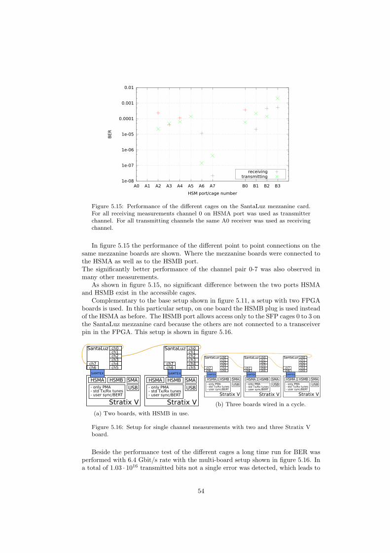
1e-08
1e-07
1e-06
1e-05
0.0001
0.001
0.01
A0 A1 A2 A3 A4 A5 A6 A7 B0 B1 B2 B3
BER
HSM port/cage number
receivingtransmitting
Figure 5.15: Performance of the different cages on the SantaLuz mezzanine card.For all receiving measurements channel 0 on HSMA port was used as transmitterchannel. For all transmitting channels the same A0 receiver was used as receivingchannel.
In figure 5.15 the performance of the different point to point connections on thesame mezzanine boards are shown. Where the mezzanine boards were connected tothe HSMA as well as to the HSMB port.The significantly better performance of the channel pair 0-7 was also observed inmany other measurements.
As shown in figure 5.15, no significant difference between the two ports HSMAand HSMB exist in the accessible cages.
Complementary to the base setup shown in figure 5.11, a setup with two FPGAboards is used. In this particular setup, on one board the HSMB plug is used insteadof the HSMA as before. The HSMB port allows access only to the SFP cages 0 to 3 onthe SantaLuz mezzanine card because the others are not connected to a transceiverpin in the FPGA. This setup is shown in figure 5.16.
(a) Two boards, with HSMB in use.
(b) Three boards wired in a cycle.
Figure 5.16: Setup for single channel measurements with two and three Stratix Vboard.
Beside the performance test of the different cages a long time run for BER wasperformed with 6.4 Gbit/s rate with the multi-board setup shown in figure 5.16. Ina total of 1.03 · 1016 transmitted bits not a single error was detected, which leads to
54

a BER < 2.9 · 10−16(95%C.L.) at 6.4 Gbit/s with setup 5.16a.
5.3.4 Multi-Channel SFP
The main feature of the SantaLuz mezzanine card is to provide up to eight channelson one card, which is attached with a HSMC cable to the Stratix V developmentboard either via the HSMA or the HSMB port. Besides the performance of singlechannel optical links, the performance of the board equipped with multiple opticaltransceivers is investigated. To this end, the different cages are used at the sametime as well as all cages at the same time.
A setup of two Stratix V boards is used to measure the BER behavior if multiplechannels are used. Therefore one development board with a SantaLuz card attachedto the HSMA port is used to transmit 6.4 Gbit/s random data generated out of a8 bit PRN (see 3.4.1) generator on multiple lines. All data streams of this setupused the same random number generator with the same seed. This has to be takeninto account when the following data from these measurements are interpreted. Ina later setup described in 5.3.4 this disadvantage was removed and different seedswere used for each channel.Extensive tests were performed with permutations using between one and up to fivelines at the same time. Figure 5.17 shows the performance if two receivers are oper-ated at the same time and the data are transmitted from a second FPGA with 6.4Gbit/s. Some channel combinations introduce bit errors. Figure 5.17b shows thebehavior of the cards if all channels are in use, but only two channels are used tomeasure their bit error rate. The results of the complete measurements with up tofive parallel channels are listed in table A.1 in section Appendix.The measurements show that some channels behave much worse than others witherror rates up to 10−6. With this setup, the measurements with four and five chan-nels operating in parallel show a better performance than the measurements whereonly two or three channels are used. This observation is not completely understood.It can be speculated that this behavior is related to the fact that the data gener-ators produce all the same pseudo random numbers in phase. The bottom line ofthe measurements is that the setups cannot be operated with multiple transceiverswithout any further analog tuning or DC balancing.
55

0 1 2 3 4 5 6 7
channel
0
1
2
3
4
5
6
7
channel
1e-12
1e-10
1e-08
1e-06
0.0001
0.01
1
BER
(a) BER with two active receivers. The datais sent from a second FPGA.
0 1 2 3 4 5 6 7
channel
0
1
2
3
4
5
6
7
channel
1e-10
1e-08
1e-06
0.0001
0.01
150m cable
1m cable
BER
(b) All channels in use, one pair measured atthe time with 1 m (under diagonal) respec-tively 50 m cables (upper diagonal). No mea-surements were performed for the white areain the upper part.
Figure 5.17: BER measurements at 6.4 Gbit/s to quantify cross talk between thechannels.
Multi-Channel Analog Tuned BER Tests
(a) analog tuned BERT(b) Toolkit setup
Figure 5.18: Setup for analog tuned transceivers.
To test the system as a whole, a setup as shown in figure 5.18a is used with differentparameters. The range for optimal analog tune values for the transmitter in theFPGA PMA were obtained from scans with the Altera transceiver toolkit describedin 5.2.3. These values are optimized further during the set up to decrease BER in allchannels. To have full control over all elements, the PMA is the only used IP hardcore, no hard core PCS is used. As before, the synchronization and bit error testare performed in user logic according to the concepts described in section 5.2.1 and5.2.2. The data generator produces pseudo random numbers based on sequences ofdifferent length. For each channel, a different seed is chosen to ensure that the bitstreams on all channels are different. The length of the PRN sequence has a directinfluence on the maximal number of identical bits in a row as well as on how DCun-balanced the data stream is.
56
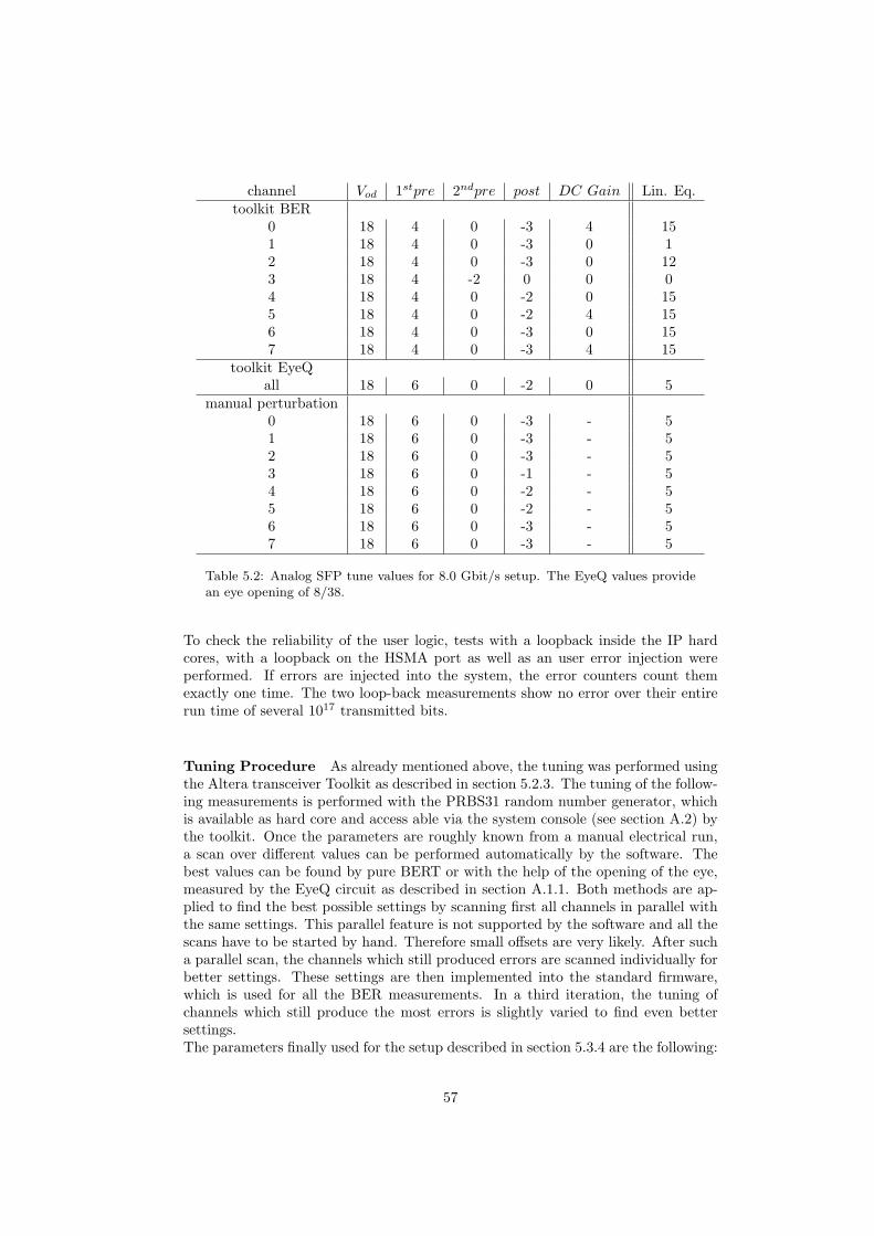
channel Vod 1stpre 2ndpre post DC Gain Lin. Eq.toolkit BER
0 18 4 0 -3 4 151 18 4 0 -3 0 12 18 4 0 -3 0 123 18 4 -2 0 0 04 18 4 0 -2 0 155 18 4 0 -2 4 156 18 4 0 -3 0 157 18 4 0 -3 4 15
toolkit EyeQall 18 6 0 -2 0 5
manual perturbation0 18 6 0 -3 - 51 18 6 0 -3 - 52 18 6 0 -3 - 53 18 6 0 -1 - 54 18 6 0 -2 - 55 18 6 0 -2 - 56 18 6 0 -3 - 57 18 6 0 -3 - 5
Table 5.2: Analog SFP tune values for 8.0 Gbit/s setup. The EyeQ values providean eye opening of 8/38.
To check the reliability of the user logic, tests with a loopback inside the IP hardcores, with a loopback on the HSMA port as well as an user error injection wereperformed. If errors are injected into the system, the error counters count themexactly one time. The two loop-back measurements show no error over their entirerun time of several 1017 transmitted bits.
Tuning Procedure As already mentioned above, the tuning was performed usingthe Altera transceiver Toolkit as described in section 5.2.3. The tuning of the follow-ing measurements is performed with the PRBS31 random number generator, whichis available as hard core and access able via the system console (see section A.2) bythe toolkit. Once the parameters are roughly known from a manual electrical run,a scan over different values can be performed automatically by the software. Thebest values can be found by pure BERT or with the help of the opening of the eye,measured by the EyeQ circuit as described in section A.1.1. Both methods are ap-plied to find the best possible settings by scanning first all channels in parallel withthe same settings. This parallel feature is not supported by the software and all thescans have to be started by hand. Therefore small offsets are very likely. After sucha parallel scan, the channels which still produced errors are scanned individually forbetter settings. These settings are then implemented into the standard firmware,which is used for all the BER measurements. In a third iteration, the tuning ofchannels which still produce the most errors is slightly varied to find even bettersettings.The parameters finally used for the setup described in section 5.3.4 are the following:
57

loopback transmitted bits BER limit (95%C.L.)SFP internal 1.2 · 1017 < 1.7 · 10−17
SFP external 1.3 · 1017 < 1.9 · 10−17
QSFP internal 5.1 · 1017 < ·10−17
Table 5.3: 8.0 Gbit/s SFP and 11.3 Gbit/s QSFP loopback measurments.
Loop Back Measurements Measurements without any physical attachment areperformed to review the performance of the user logic as well as the one of theStratix V. One setup with a loopback inside the IP hard core as well as one witha loopback on the HSMA port are performed. In a loopback the receiver channelsare attached directly to the transmitter of the same channel. For the IP hard coreinternal loopback the same tune values as for all the other tests are used. The HSMCloopback measurement with a loopback header could only be performed without anytuning. This can be explained by the fact that in the setup with optical transmission,the optical receiver acts as an electrical amplifier (see 5.1.3).
This measurements together with the correct detection of all induced errors showthat the used setup is reliable for BERT down to an order of 10−17 if all channelsare used at 8.0 Gbit/s.
PRN length dependency The BER of 8.0 Gbit/s data transmission with theabove described setup, where the transceiver are tuned as described, depends highlyon the used data patterns. Pseudo random generators are a good tool to test forall possible data patterns. At data rates around 8.0 Gbit/s even all permutationsof 31 bit PRN are tested once in less than a minute. Without any further modifica-tion, the synchronization conditions described in chapter 5.2.1 are not met for PRNwhich are generated out of more than 14 bits. Simulations of the running disparitybehavior of the different patterns used are shown in figure 5.19.If a running disparity controller is added to the logic, the transmission quality in-creases as is shown in table 5.4. In addition to this controller, tests with an additionalscrambler are also performed.
58

-800
-600
-400
-200
0
200
400
600
800
1000
0.0 0.2 0.4 0.6 0.8 1.0
runnin
g d
ispari
ty
period
RD40(PRBS31)RD80(PRBS31)Random [*e-3]PRBS31 [*e-3]101010...RN14101010....RN7 PRBS7
Figure 5.19: Running disparity of different data patterns. The period length foreach pattern generated out of l bits is 2l − 1. The absence of the only zero patternin random number generators (see 3.4) based on LFSR introduces a systematicaldisparity offset, which is corrected for in this figure. Zero-one alternating patternfollowed by 7 bit generated RN run error free without any further disparity controlat 8.0 Gbit/s, for 14 bit generated patterns synchronization still holds according tothe definitions in section 5.2. For patterns with larger l disparity control (RD) arerequired.
In figure 5.19 a much better random number generator with 80 bits (RD80) isadded to the simulation. It can be seen, that it performs better than the PRBS31generators regarding running disparity .
Running Disparity This option controls the disparity of each 80 bit word sent.As described in 5.3.4, the parity of a data word is the inbalance between ones andzeros. The running disparity control uses the highest bit of each transmitted dataword to indicate whether the data of this particular word is inverted or not. Depend-ing on the running disparity, the continuously summed up disparities, the controldecides whether the actual word is inverted or not. This method adds an overheadof 1 bit and some additional latency in the transmitting logic. Summing over allbits in FPGA logic is a time critical process. The gain is a limitation of the runningdisparity to values between ± (wordlength-1). In the used firmware, the full PMAwidth of 80 bits is utilized in RD80 and two parallel controllers each with 40 bitsare implemented in RD40. Longer words decrease the speed of the whole user logic,which allows an easier adaption to higher serial data transmissions.
Scrambler As described in section 2.2.3 a scrambler ensures that the probabilityof getting a very unfavorable bit pattern in random distributed data is decreasedstrongly. The implemented scrambler is a very primitive version whose state iscalculated out of two taps from the incoming data. In such a scheme, the scrambleris aligned after the number of data length bits and does not need any additional
59

synchronization. The use of a scrambler can multiply errors due to bit flips if theyoccur at the bit, which is used as tap for the scrambler. An error out of such a bitflip would stay in the scrambler state for the number of word lengths and count asone error for each word.
BER Values In table 5.4 longterm measurements with tuned transceiverss at 8.0Gbit/s with different cables, with and without scrambler and disparity controllerare summarized. Beside this measurements with 31 bit generated random numbergenerators, different other patterns are evaluated. Patterns composed of alternatingones and zeros, e.g. “10101010”, followed by a dedicated number of bits with arandom number generator are used. Transmission without any errors (BER <6.0·10−17) are possible with random number generators up to 7 bits, synchronizationis achieved with generators up to 14 bits. For all pattern generated with longergenerators, disparity control is needed.
ch RD80, no Sc l=50m RD40, no Sc l=1m RD80, Sc l=50m0 < 1.5 · 10−13 (7.24± 5.12) · 10−16 < 1.4 · 10−15
1 < 1.5 · 10−13 (4.56± 0.05) · 10−13 < 1.4 · 10−15
2 (1.03± 0.07) · 10−11 (4.61± 0.04) · 10−12 (1.83± 0.008) · 10−12
3 (8.32± 2.08) · 10−13 (4.00± 0.12) · 10−13 (4.20± 0.14) · 10−13
4 < 1.5 · 10−13 (1.45± 0.02) · 10−12 < 1.4 · 10−15
5 < 1.5 · 10−13 (6.72± 0.16) · 10−13 (2.93± 1.12) · 10−15
6 < 1.5 · 10−13 (2.55± 1.04) · 10−15 < 1.4 · 10−15
7 (3.95± 0.45) · 10−12 (1.70± 0.85) · 10−15 (6.08± 0.06) · 10−12
total (1.85± 0.11) · 10−12 (4.56± 0.05) · 10−13 (1.041± 0.008) · 10−12
Table 5.4: BER test with 31 bit PRN patterns at 8.0 Gbit/s with analog tunedtransceivers. Measurements with and without scrambler (SC). Measurements with-out disparity controller RD are not possible because no synchronization accordingto the conditions in 5.2.2 is achieved. All stated upper limits are 95%C.L. values.
In addition to the measurements shown in table 5.4 with 8.0 Gbit/s, the rate towith the transceivers are tuned, measurements at 6.4 Gbit/s with the same analogtune values were performed. The results of these measurements are summarized intable 5.5. Setups with running disparity control, but non-tuned transceivers, staysynchronized according to the requirements mentioned in section 5.2. Neverthelessthey show BER of the order 10−4, hence they can not be used with this settings.
5.3.5 Optical QSFP Links
The QSFP cages on the Stratix V development board are used to setup a card-to-card connection between two boards. This is realized with the Molex transceiver andoptical fiber system as described in section 5.1.3. The used firmware correspondsto the one used for all multi-channel test in section 2.1.2 for the SFP channels. A80 bit width hard core PMA is fed with pseudo random numbers generated out ofa 31 bit state. The running disparity is in addition controlled on a ±40 bit base.Table 5.6 summarizes the performed measurements. The 9.3 Gbps transmissions areperformed without any analog tuning. However the 11.3 Gbps transceivers are tunedaccording to the values obtained in section 5.3.5. Synchronization is only achievedwith a 80 bit disparity control.
60

ch no RD l=1m RD80 l=1m RD80 l=50m RD40 l=1m0 (6.98± 0.01) · 10−3 < 7.8 · 10−16 < 4.9 · 10−16 < 7.8 · 10−16
1 (8.81± 0.01) · 10−3 < 7.8 · 10−16 < 4.9 · 10−16 < 7.8 · 10−16
2 (7.79± 0.03) · 10−11 < 7.8 · 10−16 < 4.9 · 10−16 < 7.8 · 10−16
3 (2.23± 0.10) · 10−2 < 7.8 · 10−16 < 4.9 · 10−16 < 7.8 · 10−16
4 (9.57± 0.01) · 10−10 < 7.8 · 10−16 < 4.9 · 10−16 < 7.8 · 10−16
5 (9.72± 0.10) · 10−12 < 7.8 · 10−16 < 4.9 · 10−16 < 7.8 · 10−16
6 (3.81± 0.01) · 10−10 < 7.8 · 10−16 < 4.9 · 10−16 < 7.8 · 10−16
7 (1.61± 0.01) · 10−10 < 7.8 · 10−16 < 4.9 · 10−16 < 7.8 · 10−16
total (4.85± 0.01) · 10−3 < 9.8 · 10−17 < 6.1 · 10−17 < 9.8 · 10−17
Table 5.5: BER test with 31bit PRN pattern at 6.4 Gbit/s with transceivers whichare analog tuned for 8.0 Gbit/s. Upper limits are 95%C.L. values.
rate cable length BER9.3 3 < 9.29 · 10−17
9.3 20 < 9.56 · 10−17
11.3 20 (3.29± 1.04) · 10−16
11.3* 20 (turned) (3.71± 0.31) · 10−15
11.3+ 20 < 9.45 · 10−17
Table 5.6: QSFP BER measurements with 80 bit disparity control. *Replaced badreceiving FPGA and turned cable. +Used two new FPGAs.
The operation at 11.3 Gbit/s with tuned transceivers shows errors in one of theeight, four in each direction, channels for some FPGAs. The performance of thischannel is BERS04 = (3.32 ± 0.74) · 10−15, BERS11 = (2.97 ± 0.24) · 10−14 andBERS11 < 9.45 · 10−17, depending on the Stratix V board used. Different cablesand setups have been used to identify the source of the problem. Out of the 4 usedFPGAs, 2 show errors in the same receiving channel. Once a problematic channel isidentified, the others can in principle still be operated with a BER below < 4.8·10−17
(95 % C.L.).
QSFP Analog Tuning
Analog tune values are gained out of a swap test with the Altera transceiver toolkitin the same way as for the optical SFP links. Several tune value ranges with excellentBER are listed in table 5.7. For the 11.3 Gbit/s tests the values at the table bottomare used.
5.4 Discussion
Transmission quality checks have been performed with two different device families.On one hand, optical SFP transceivers on SantaLuz mezzanine boards with up to 8channels are tested. On the other hand, on-board QSFP cages with cable assemblieswhich bundle four fibers have been used.
61
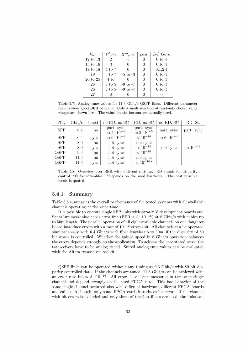
Vod 1stpre 2ndpre post DC Gain12 to 13 2 -1 0 0 to 413 to 16 3 0 0 0 to 417 to 18 4 to 7 0 0 0,1,2,4
19 3 to 7 -5 to -3 0 0 to 420 to 25 4 to 0 0 0 to 4
26 3 to 5 -9 to -7 0 0 to 426 3 to 5 -9 to -7 0 0 to 427 8 0 0 0
Table 5.7: Analog tune values for 11.3 Gbit/s QSFP links. Different parameterregions show good BER behavior. Only a small selection of randomly chosen valueranges are shown here. The values at the bottom are actually used.
Plug Gbit/s tuned no RD, no SC RD, no SC no RD, SC RD, SC
SFP 6.4 nopart. sync part. sync
part. sync part. sync≈ 5 · 10−4 ≈ 3 · 10−5
SFP 6.4 yes ≈ 6 · 10−4 < 10−16 ≈ 6 · 10−4 -SFP 8.0 no not sync not sync - -SFP 8.0 yes not sync ≈ 10−12 not sync ≈ 10−12
QSFP 9.3 no not sync < 10−16 - -QSFP 11.3 no not sync not sync - -QSFP 11.3 yes not sync < 10−16* - -
Table 5.8: Overview over BER with different settings. RD stands for disparitycontrol, SC for scrambler. *Depends on the used hardware. The best possibleresult is quoted.
5.4.1 Summary
Table 5.8 summaries the overall performance of the tested systems with all availablechannels operating at the same time.
It is possible to operate single SFP links with Stratix V development boards andSantaLuz mezzanine cards error free (BER < 3 · 10−16) at 8 Gbit/s with cables upto 50m length. The parallel operation of all eight available channels on one daughterboard introduce errors with a rate of 10−12 errors/bit. All channels can be operatedsimultaneously with 6.4 Gbit/s with fiber lengths up to 50m, if the disparity of 80bit words is controlled. Whether the gained speed in 8 Gbit/s operation balancesthe errors depends strongly on the application. To achieve the here stated rates, thetransceivers have to be analog tuned. Suited analog tune values can be evaluatedwith the Altera transceiver toolkit.
QSFP links can be operated without any tuning at 9.3 Gbit/s with 80 bit dis-parity controlled data. If the channels are tuned, 11.3 Gbit/s can be achieved withan error rate below 3 · 10−16. All errors have been measured in the same singlechannel and depend strongly on the used FPGA card. This bad behavior of thesame single channel occurred also with different hardware, different FPGA boardsand cables. Although, only some FPGA cards introduces bit errors. If the channelwith bit errors is excluded and only three of the four fibers are used, the links can
62

be operated error free as well. How to proceed with these slightly worse channels isapplication dependent.
The data rates achieved in this thesis are sufficient to realize the Mu3e readoutchain as proposed and shown in figure 1.8 for phase II. Only these very high datarates resulting in a high total bandwidth of the DAQ make the Mu3e trigger-lessdetector and GPU reconstruction design possible.
5.4.2 Crucial Points
Based on the measurements in this thesis as well as the experience with the hardwarethe following points are considered crucial.
Cable Length
A BER dependency on cable length has never been observed. Multi-mode fibersbetween 0.5m and 50m and single mode fibers between 1m and 20m have beenused. It has to be mentioned, that no cables longer than specifications allow haveever been used. Particularly, multi-mode fibers of the given quality (OM2) arespecified exactly up to the used 50m.
Cross Talk in SantaLuz Boards
The SantaLuz boards are the bottlenecks in the current SFP setup. The Samteccables are specified for higher data rates than used, only the mezzanine board hasnever been used at these rates. It seems that the bit errors are introduced bycross talk on the board. This effect can be minimized by an analog tuning of thetransceivers. Unfortunately, this affects only the transmitting part. The optical SFPreceivers output signal can not be modified. Cross talk induced by the receiving lineson the boards can thus not be addressed at the moment.
Improvement Due to Disparity Controller and Scrambler
Different measurements with a simple scrambler and disparity controllers are per-formed. Disparity was controlled within 40 and 80 bits. Neither 8.0 Gbit/s nor 6.4Gbit/s links work properly if all channels are used without a disparity controller.At 8.0 Gbit/s the state machines synchronization criteria are not met, at 6.4 Gbit/ssynchronization is achieved but bit errors occur with a rate of 10−3 errors/bit whichmakes the links unusable.
Simulations with the used pseudo random number generators show that the run-ning disparity can be very unbalanced. Results are shown in figure 5.19. The absoluterunning disparity is not of interest, the inbalance over a given time range is the criti-cal value. How inbalanced signals over which time ranges are acceptable, is unknownat the moment. But a disparity control on a 80 bit base seems to be sufficient for allkinds of data patterns. Patterns without disparity control are possible for alternat-ing zero-one pattern followed by 7 bit generated random numbers. Synchronizationwithout disparity control is achieved up to an alternating pattern followed by 14 bitgenerated random number. For rates of 8.0 Gbit/s a slight decrease in BER canbe observed if the running disparity is controlled within 40 bits. Nevertheless, the
63

result does not improve significantly with a factor of ∼ 5 at 8 Gbit/s. Only changesof orders of magnitudes are considered significant in this scope.
As described in 5.2.2, every possible bit pattern of 32 bits is tested hundredsof times. An additional scrambler which would only decrease the probability ofdisadvantageous pattern does not improve the signal quality.
For every transmission with the used optical links a running disparity controlover maximum of 80 bits is required. This is also true for QSFP links.
Physical Coding Sublayer (PCS)
Different PCS have been used in the development process of the firmwares. Theavailable PCS are very useful if a existing protocol is implemented. Standard logicperforms equally well for parts where the data can be handled parallel and offersmore flexibility. PCS are very device specific, whereas user logic is more easilyportable. The hard core PCS free some logic cells.
BERs Relevance for the Experiments
The performed measurements have aimed at a bit error rate below 3 · 10−16. Thisorder of magnitude is mainly motivated by the time needed for the measurements.Single lines at 8.0 Gbit/s have to be operated for two weeks. Assuming a total datarate of the whole detector of 1 Tbit/s this rate limit translates to approximately 1error per hour, which is orders of magnitudes less than for example noise hits.
64

Chapter 6
Readout Chain FirmwareComponents
Besides the fast optical transmission between different components of the Mu3ereadout chain, some selected firmware components are investigated. There are on onehand the implementation of the event time ordering in the front-end FPGAs for theMuPix sub-detector, and on the other hand the potential coordinate transformationon FPGA cards inside the filter farm computers. These two readout chain aspectsare described and tested in the following.
6.1 Front-End FPGA
Front-end FPGAs receive hit data from MuPix pixel sensors. The hits are encodedin 24 bits, 8 bit each for row and column information as well as an 8 bit Gray codetimestamp. The timestamps have to be decoded into binary numbers in order todetermine the relative timing of hits. In addition to the hit data, the FPGA has toknow the current timestamp of the whole system. This can be realized either withan own Gray counter or by receiving timestamps from the sensors. A combinationof these two concepts would allow some cross checks whether the counters are stillaligned.
The timestamp sorting is realized in a buffer. The goal is to output time orderedhit information packages. How the ordering is realized best depends on the structureof the received hits and the hardware used. Due to space requirements and costs, itis foreseen to use relatively small FPGAs without large memory blocks.
In the following, the structure of the hit data is discussed. Followed by two dif-ferent concepts how the data could be buffered and time ordered. This is completedby a comparison of the two previously introduced concepts.
6.1.1 Hit Data Structure
When a pixel in the MuPix sensor is hit, its address is stored together with a cor-responding timestamps in a column wise queue for further readout. The readoutprocess (see A.4) loads one hit per column into a readout buffer. These hits aretransmitted one after another via the serial interface. New hits occurring duringthis time, are added to the queue. Once the readout buffer is empty, maximal
65

one hit is load again from each column. This readout scheme results in disorderedtimestamps. Many hits per sensor introduce hits with long delayed timestamps.
The received hit data have always a timestamp of the current or older timestamps.The maximal delay is denoted D. After each readout of a bucket of data, the offsetbetween the timestamp of the received hits and the one at the start of a new bucketis called T. If the buffer is read every D frames, T is in the range of −D to +D. Thenumber of hits per frame has an influence on the number of hits which has to bestored. The average number is denoted N and the maximal expected number Nmax.
6.1.2 Concept I
For each possible time offset T between −D and +D memory for Nmax hits, columnand row corresponding to 16 bits, is reserved. The timestamp is encoded in thestorage address. The required memory size is given by:
BRAM = Nmax · 2D · 16bits (6.1)
6.1.3 Concept II
The hit data, row and column, are stored in a ring buffer with a data depth of 16 bitsand a length of D ·N . In addition one register per possible time offset T with a depthof the length of the previously mentioned hit data memory exists. In the registercorresponding to the timestamp offset of a hit, the bit number which corresponds tothe address the data has in the hit memory is set to 1. In the reading process, theregisters are read descending in the register and the hit data of all memory addresses,which are marked with a 1 in the current register, are read (see figure 6.1b). Thisresults in time sorted outputs. The memory required for this concept is given by:
BRAM = N ·D · 16bits (6.2)
BREG = N ·D · 2D · bits (6.3)
6.1.4 Comparison
Simulations have shown that N is maximal of the order 5 and up to 3 · 1.25 Gbit/sLVDS data links cause bandwidth limitations the possible read out of hit data(24bits) per 50 ns frame of 2.1 hits/frame. Nevertheless, the maximal number ofhits with the same timestamp can be much larger, because they can be distributedover D readouts. A value of Nmax = 30 seems to be on the conservative side. Max-imal delays D of 30 are expected, as described in 1.3.2. Under these assumptions,concept II is favored with 11’400 bits over 28’800 bits of concept I. Concept II hasbeen implemented into a Stratix V FPGA and has been simulated with ModelSim.
6.2 Coordinate Transformation on FPGAs
As described in section 1.3 the pixel hit data will be transformed on the FPGAlocated inside every PC in the filter farm from pixel address and hit coordinatesinto a global coordinate system. The conversion from integer pixel addresses andhit coordinates into single precision floating point numbers on FPGAs is discussed
66
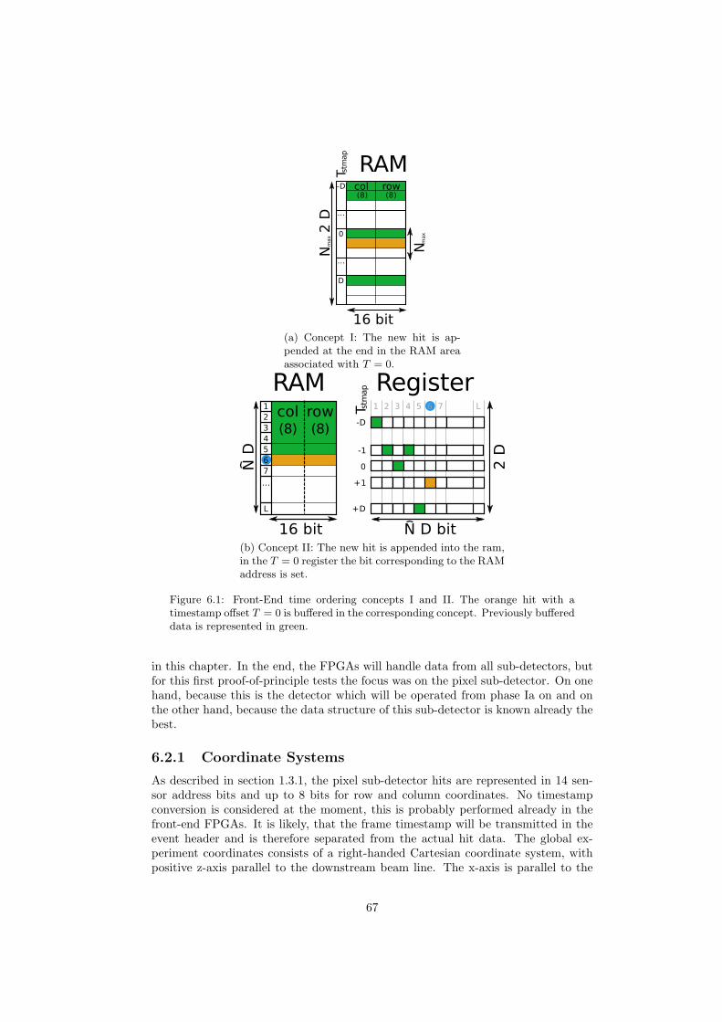
(a) Concept I: The new hit is ap-pended at the end in the RAM areaassociated with T = 0.
(b) Concept II: The new hit is appended into the ram,in the T = 0 register the bit corresponding to the RAMaddress is set.
Figure 6.1: Front-End time ordering concepts I and II. The orange hit with atimestamp offset T = 0 is buffered in the corresponding concept. Previously buffereddata is represented in green.
in this chapter. In the end, the FPGAs will handle data from all sub-detectors, butfor this first proof-of-principle tests the focus was on the pixel sub-detector. On onehand, because this is the detector which will be operated from phase Ia on and onthe other hand, because the data structure of this sub-detector is known already thebest.
6.2.1 Coordinate Systems
As described in section 1.3.1, the pixel sub-detector hits are represented in 14 sen-sor address bits and up to 8 bits for row and column coordinates. No timestampconversion is considered at the moment, this is probably performed already in thefront-end FPGAs. It is likely, that the frame timestamp will be transmitted in theevent header and is therefore separated from the actual hit data. The global ex-periment coordinates consists of a right-handed Cartesian coordinate system, withpositive z-axis parallel to the downstream beam line. The x-axis is parallel to the
67
experimental hall floor and y points towards the roof. Distances are stored in singleprecision IEEE floating point format and given in mm.
6.2.2 The Transformation
The transformation of a hit in sensor s in the pixel ~k = (col, row)T is given by
xyz
= ~x = ~Os + Ts~k =
oxsoysozs
+
xcs xr
s
ycs yrszcs zrs
(
colrow
)
(6.4)
where ~Os is the origin vector of sensor s and Ts the sensors orientation. Thistransformation is implemented in 4 steps in hard core DSP blocks on the FPGA.
Integer to Float 6 cycles are needed to transform the integer col and row coordi-nates to single precision floating point numbers (Fmax = 515 MHz [66]).
Multiplication x, y and z coordinates from col and row contribution are calculatedin parallel. This 6 parallel multiplications, corresponding to the first part ofthe matrix multiplication in 6.4, can be implemented in 5, 6, 10 or 11 cycles(Fmax = 445 MHz, for 11 cycle implementation [66]).
Addition 1 The contributions for each Cartesian coordinate from col and rows areadded up. This step finishes the matrix multiplication and can be implementedselectively between 7 and 14 cycles (Fmax = 495 MHz, for 14 cycle implemen-tation [66]).
Addition 2 In a last step, the sensors origin vector is added in parallel for eachcoordinate component. This addition can be implemented again with between7 and 14 cycles (Fmax = 495 MHz [66]).
A transformation needs between 26 and 46 clock cycles. The more cycles are spent,the faster clock rates are possible, but more logic cells are consumed.
6.2.3 The Implementation
The above described transformation is implemented with VHDL and its simulationis shown in 6.2. To achieve the maximal speed, the shown version is implementedfully pipelined with 46 cycles. The sensors origin vectors and their orientation arestored in ROM (see 3.2.4). For each sensor, addressed with 14 bits according to theproposed address scheme, 9 times a 32 bit single precision floating point numberis stored. Namely, the origin vector with its three coordinates as well as row andcolumn direction with another 3 coordinates each. This results in a ROM size of214 · 9 · 32 bits = 214 · 288 bits = 4′718′592 bits.
Multiplications as well as additions provide an overflow and underflow detectionwitch rises an error flag at the output.
The above described implementation uses 3′227 ALMs (1.8 %), 4′740 registers(1.3 %), 6 DSP (0.4 %) hard cores and 4′718′592 (11.4 %) bits block memory pertransformation component. The values in brackets represent the fraction used in aStratix V FPGA with 230’000 ALMs (see 5.1).
68

1 7
18 30
44 45 49 51 53
0-1
Figure 6.2: ModelSim simulation of a coordinate transformation on a FPGA. After the release of the active low reset RST in cycle 0, hitdata are loaded. In Cycle 1 the address, col and row information are separated. pixel row i shows that the eighth row of the sensor was hit.This integer is converted to an single float representation in 6 cycles. In cycle 7, the row coordinate pixel row f in single float representation0x4100000, which represents the number 8, as well as the transformation coefficient for row-x row x 0x372C5AC which corresponds to 1 ·10−5
are ready. The multiplication takes 11 cycles and is ready in cycle 18 as x row with a hexadecimal value of 0x38A7C5AC, correspondingto 1 · 10−5. All other row, col and coordinate combination are ready at the same time. The col and row contribution to each coordinatecomponent are summed up in the next 14 cycles. There product x trafo is ready in cycle 30 and has the value 0x3ACB295F, correspondingto 1.55 · 10−3. In the same cycle the sensors origin coordinate are loaded and added to the previously calculated coordinate contributionsin another 14 cycles. In cycle 44 the final coordinates are ready and output in the next cycle together with a valid and error flag. If themultiplication or the two additions result in an overflow or underflow, simulated in hit data loaded in cycles 5, 7 and 9 the error flags in therorresponding output cycles 49, 51 and 53 indicate this.
69

ROM address depth 1 2 3 4 6 8 12 2415 (2 x MuPix) 448 360 38114 (MuPix) 412 445 367 344 285
13 (1/2 MuPix) 464 431 424 363 30712 (1/4 MuPix) 469 417 319 292 328
Table 6.1: Fmax for different coordinate transformation implementations in a StratixV FPGA with different number of parallel implementations and different ROMdepths. 14 bits corespondents to the MuPix sub-detector address space. The con-figurations in bold could handle the whole detector.
6.2.4 Performance
The maximal clocking frequency of the different components are given in bracketsin the list 6.2.2. It has to be mentioned that for Fmax of adders and multipliersspecifications only for Stratix IV and lower are available [88]. The ROM used tostore the transformation coefficients is specified up to 600 MHz [69, p. 14]. Inprinciple operation speeds up to 445 MHz should be possible. Table 6.1 showsTimeQuest results of different implementations. Multiple coordinate transformationcomponents have been implemented in parallel as well as components with smallerROM. This is motivated by the fact, that if the filter farm PCs get the raw data ondifferent lines, the lines probably deliver data only from a sub-part of the detector.To include the other sub-detectors a version with twice the address space was usedas well. The number of parallel implemented components is limited by the availableinternal memory to 7.
6.2.5 Conclusion
The implementation and simulation of coordinate transformation components in anStratix V FPGA has proven the concept and confirmed the speed stated in theAltera manuals. The same order of speed is still achievable if multiple componentsare implemented in parallel. The limitations of how many parallel components can beused, comes from the available FPGA internal memory that is supposed to store allthe transformation coefficients. External memory in Stratix V development boardsare specified almost with the same speed as the internal. Hence, this memory couldin principle be used as well.
The possible clock rates of approximately 400 MHz is sufficient to handle 30 bitlong hit data transmitted with 12 Gbit/s. This transmitting speed is the very upperlimit that will ever be used in the Mu3e experiment. One coordinate transformationper transceiver is sufficient for all phases of the Mu3e experiment.
70

Chapter 7
LVDS on Kapton FlexPrints
The Mu3e pixel sub-detector readout chain includes LVDS links on Kapton flex printsbesides fast optical links. As a part of this work, a proof of principle is providedthat such cables can be produced in-house with freshly acquired tools. This chapterintroduces the used materials and tools, explains the used test pattern as well as theminimal achieved structure sizes. At the end, concrete ideas for subsequent worksare provided.
7.1 Kapton
Kapton is a polyimide film developed by DuPoint with a unique combination ofelectrical, thermal, chemical and mechanical properties [89]. As described in section1.2, Kapton is used in the detector’s active region as mechanical support structure aswell as substrate for aluminum traces. Kapton is used mainly to minimize the amountof material inside the detector, and consequently to reduce multiple scattering [11].
Regarding thermal properties, no melting point is known for Kapton Type 100HNfilms [90, table 2]. Furthermore, it remains stable in a temperature range between−269 C to 400 C [91]. Regarding electrical properties, Kapton’s dielectric constantsvaries linearly with the relative humidity between 3.0 and 3.8 and drops in a tem-perature range between 0 C and 200 C nearly linearly from 3.5 down to 2.9 [90,figure 11, 15].
In the present thesis 25 µm Kapton Type 100HN metallized with aluminum of50 nm respectively 25 µm is used.
7.2 Low-Voltage Differential Signaling (LVDS)
Low-voltage differential signaling (LVDS) is the specification of a serial differentialsignal scheme. LVDS transmitting lines consist of a pair of wires. The transceiverinjects a constant current of 3.5mA. The current direction indicates the logic state ofthe transition line. The impedance of the two lines is 100 Ω. To minimize reflections,they are terminated with an identical resistance. Therefore, the differential voltage,which is detected on the receiver side, is V = R · I = 350mV . The polarity of thisvoltage indicates the logic state.
The implementation of two traces close to each other that carry an equal currentin opposite directions minimizes the emission of electromagnetic noise. The induced
71

Figure 7.1: LVDS cable profile used for impedance calculations in equation 7.1.
noise is reduced as well because it is approximately the same in both wires, whichis canceled by the differential approach. Furthermore, LVDS consumes very littlepower and the power supply requirements can easily be met due to the constantcurrent flow.
The impedance of a LVDS wire pair is calculated as shown in equation 7.1 [28]for fractions of w/h between 0.1 and 3.0. Figure 7.1 shows the corresponding LVDSline and ǫr represents the substrate’s dielectric constant.
Zd =174√
ǫr + 1.41ln
(
5.98 · h(0.8 · w + t)
)(
1− 0.48exp
(
−0.96dh
))
(7.1)
For the 25 µm Kapton film coated with 50 nm respectively 25µm aluminum andKapton’s dielectric constant of ǫr = 3.5 two LVDS lines have to be w7µm = 60µmrespectively w25µm = 50µm width for d between 0.1 mm and 1 mm. These valuesare required by the fact that LVDS foresees a 100 Ω differential impedance.
7.3 Laser Platform
The Kapton aluminum processing was performed with a PLS6MW laser platformfrom Universal Laser System, which supports the use of both a 50W CO2 laserat 9.3 µm and a 40W fiber laser at 1.06 µm. Both laser types are operated in apulsed mode. The platform allows the adjustment of the laser movement speed,power, frequency, focus position in z direction and type of wave. If not only singlelines (one movement of the laser) are required, but also areas are treated, additionalvalues for contrast, definition and density can be set. These values characterize theraster behavior [92].
Beside a powerful smoke funnel, the apparatus provides a gas flow directed atthe cutting, i.e. evaporation, point. The system was operated with air. In principleevery other gas, advisably fire-proof, could be used easily. If light materials, suchas plastic films, are used this additional airflow prevents the material from burning,but can also blow it away. Hence, sticky rubber mats are used as support structure.
The delivered software and drivers allow the use of the laser platform like anyarbitrary printer. In principle, any vector format can be used as an input.
72

(a) Aluminum side. (b) Kapton side.(c) Comparison 50 nm (l.) and 25 µm (r.) Al.
Figure 7.2: 25 µm Kapton film with 50 nm/25 µm aluminium on top.
(a) Structure size and orientation test pattern.
(b) Kapton cable structures test pattern.
Figure 7.3: 25 µm Kapton film with 25 µm aluminum on top. Different test pattern.
7.4 Proof of Concept
The laser cutting machine described before could be used for Kapton flexprint fabri-cation. To produce reasonable LVDS links on a Kapton support structure, one shouldbe able to create structures on a 50 µm scale. This is required by the targeted differ-ential impedance of 100 Ω as well as space considerations inside the detector. Thegoal is to evaporate the aluminum with the laser system without damaging the un-derlying Kapton structure. For cables, the remaining aluminum has to be connectedover relatively long distances of up to 30 cm. In a first step, the evaporation of thealuminum while preserving the Kapton is tested. The treatment of areas rather thansimple cuts need significantly different settings. Once a good setting range is found,tests with different structure sizes and orientations are performed.
73

type power speed freq. z wave contrast definition density[%] [%] [MHz] [mm] [%] [%] [%]
area, 50nm 100 45 76 1.5 0 20 10 80cut, 50nm 100 7 30 1.5 - - - -area, 25µm 95 40 30 1.5 0 20 10 80area*, 25µm 100 30 30 1.5 0 20 10 80cut, 25µm 100 7 30 1.5 0 - - -
Table 7.1: Used values for laser cutter to produce small structures in Al on Kapton.*These values are better suited for small structures, e.g. between two pads in figure7.3b.
Aluminum Evaporation
Aluminum’s melting point is at 660 C and it evaporates at 2519 C. Its reflectivityaround 1 µm lies in a range between 0.86 and 0.97 whereas around 10 µm it liesaround 0.98. To deploy as much laser energy as possible into the aluminum, thefiber laser with its wavelength of 1.06 µm is used [93, Fig 1].
Different Evaporation Schemes
The two tested foils have to be treated in very different ways. While the thinnerone can be handled with the Kapton side on top, this is not possible for the thickerone. The Kapton foil seems to be almost transparent at the used laser wavelength,so the energy is deposited in the aluminum layer, which then is evaporated. Figure7.2 shows the clean results which could be achieved. The comparison in 7.2c showsthe clean 50 nm vaporized Al sample, in the contrast to the thicker 25 µm glued Alsample on the right. The right Mu3e logo, manufactured with the aluminum side ontop, shows residues of burned glue.If 25 µm aluminum films are treated in the same way, not the whole Al layer evapo-rates and the gas escapes through the Kapton film. The Kapton is destroyed whilestill some aluminum remains and no electrical separation is achieved.Hence the thicker 25µm Al foil is handled with its aluminum layer to the top. Table7.1 shows the settings used for the different foils. It has to be mentioned that thefocus settings in z direction are very crucial and can vary from day to day. In orderto vary the focus, the laser cuter moves the whole stage up and down. Presumably,the zero adjustment does not work properly.
Structure Sizes
The test patterns shown in 7.3a are used to evaluate the minimal scale for producablestructures. With the patterns in figure 7.3a on one hand the ability to separatetwo elements electrically and on the other hand how small structures still provideelectrical connectivity are tested. Both kinds of scale tests are performed in bothdirections, parallel and perpendicular to the laser carrier’s motion. With the bestsettings as stated in table 7.1, the following minimal structure sizes could be realized:
74
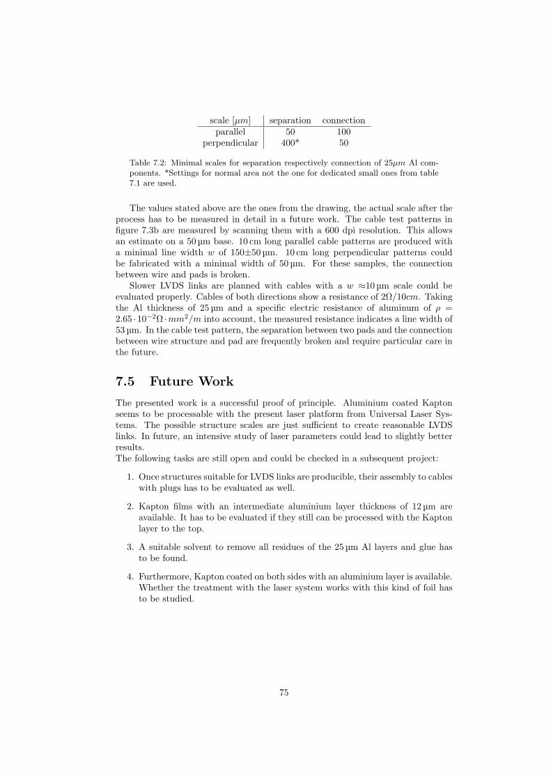
scale [µm] separation connectionparallel 50 100
perpendicular 400* 50
Table 7.2: Minimal scales for separation respectively connection of 25µm Al com-ponents. *Settings for normal area not the one for dedicated small ones from table7.1 are used.
The values stated above are the ones from the drawing, the actual scale after theprocess has to be measured in detail in a future work. The cable test patterns infigure 7.3b are measured by scanning them with a 600 dpi resolution. This allowsan estimate on a 50 µm base. 10 cm long parallel cable patterns are produced witha minimal line width w of 150±50 µm. 10 cm long perpendicular patterns couldbe fabricated with a minimal width of 50 µm. For these samples, the connectionbetween wire and pads is broken.
Slower LVDS links are planned with cables with a w ≈10 µm scale could beevaluated properly. Cables of both directions show a resistance of 2Ω/10cm. Takingthe Al thickness of 25 µm and a specific electric resistance of aluminum of ρ =2.65 ·10−2Ω ·mm2/m into account, the measured resistance indicates a line width of53 µm. In the cable test pattern, the separation between two pads and the connectionbetween wire structure and pad are frequently broken and require particular care inthe future.
7.5 Future Work
The presented work is a successful proof of principle. Aluminium coated Kaptonseems to be processable with the present laser platform from Universal Laser Sys-tems. The possible structure scales are just sufficient to create reasonable LVDSlinks. In future, an intensive study of laser parameters could lead to slightly betterresults.The following tasks are still open and could be checked in a subsequent project:
1. Once structures suitable for LVDS links are producible, their assembly to cableswith plugs has to be evaluated as well.
2. Kapton films with an intermediate aluminium layer thickness of 12µm areavailable. It has to be evaluated if they still can be processed with the Kaptonlayer to the top.
3. A suitable solvent to remove all residues of the 25µm Al layers and glue hasto be found.
4. Furthermore, Kapton coated on both sides with an aluminium layer is available.Whether the treatment with the laser system works with this kind of foil hasto be studied.
75

Part IV
Outlook
76

Chapter 8
Outlook
In this thesis, fast optical data transmission as well as selected aspects of the read-out chain have been successfully tested. In chapter 5, the performance of differentoptical transmission methods are presented. Chapter 6 introduces concepts howthe data structure could be manipulated on different FPGA levels and chapter 7.5proofs the concept of in house Aliminum-Kapton flexprint production. These con-siderations covering very different aspects of the readout chain lead to the followingrecommendation for the data structure and for the phase Ia concept.
8.1 Readout Chain in General
It has been shown in general, that the components tested in this thesis fulfill therequirements proposed for the Mu3e read out chain. Particularly, the optical band-widths is sufficient, Kapton flexprints could in principle be produced in house andcoordinate transformation could be moved from filter farm CPUs or GPUs to FP-GAs.
8.2 Data Structure
Based on the experience with the optical links, a data structure recommendationfor the optical links of the Mu3e readout chain is presented. This recommendationfocuses on the MuPix sub-detector.
8.2.1 Starting Point
A single pixel hit can be encoded into 38 bit according to the address scheme de-scribed in 1.3.1. Multiple hits from a couple of sensors are buffered and time sortedin the front-end FPGAs. This data is sent as a package outside the detector viaoptical links. As performance tests have shown, a disparity control over 80 bit isrequired. A 64b/66b-like encoding scheme would provide the possibility to distin-guish between data words and control structures. An additional scrambler does notimprove the signal quality significantly, but complicates the synchronization process.Therefore, a scrambler is optional.
77

8.2.2 Error Detection
Due to the very low error rate, an error detection with a CRC hash could be imple-mented over rather long packages. Whenever an error is detected in such a package,the whole package has to be thrown away. If, because of bandwidth limitations,higher rates such as 8.0 Gbit/s are required, the data packages over which a singleCRC code is applied should be reduced. If errors occur more frequently, one wouldlike to drop smaller data packages.
8.2.3 Proposed Format
I propose to send the data in rather long packages, which include several frames. Theexact data width has to be adapted to the available PMA. One bit should be usedfor disparity control, further two to indicate data or control words. One dedicatedcontrol word could indicate the start of a new frame and include the correspondingtimestamp. Followed by the raw hit data with stripped-off timestamp completedwith an end of event (EOE) code word and a CRC hash. If the CRC hash does notmatch, only one frame has to be dropped. Each front-end FPGA needs slow controlas well. Small form factors are required by the experiments design. Therefore, itseems to be reasonable to include slow control information into the same opticallinks. This also ensures galvanic isolation of the detector.
8.3 Phase Ia Readout Chain
The results of this thesis show that the rate requirements of the proposed Mu3ereadout chain are met. Furthermore, the used hardware is almost sufficient to builda readout chain for phase Ia. Figures 8.1 shows the idea of such a concept.
The 38 front-end FPGA boards could be equipped with MicroPOD 14 Gbpstwelve channel parallel fiber optic modules from Avago [94]. The fibers are con-nected to SFP transceivers on SantaLuz boards of 4 Stratix V development boards.10 respectively 9 of the available 12 SFP cages are used as inputs. Two of thisfront-end FPGAs collect up-stream, two down-stream data. One SFP output canbe used to connect all four Stratix boards to a fifth one. SFP to QSFP cables fromCisco could be used therefore [95]. This fifth FPGA distributes the data with twoSantaLuz cards, which allow all together 12 SFP links to 12 PCs in the filter farm.There, the FPGA receives the data with the same SantaLuz daughter cards and putit via PCIe and direct memory access into the GPUs memory.
The bottleneck of the proposed scheme is the single fifth Stratix board whichlimits the data rate of the whole system to 4 times the operation speed of the SFPplugs. If the links are operated at 6.4 Gbit/s this results in 25.6 Gbit/s. This FPGAcould easily be doubled as indicated in green in figure 8.1. With single QSFP toquad QSFP plugs, also available from Cisco, the number of these FPGAs could evenbe six-folded. If only one additional Stratix is used, one SFP plug per read-outFPGA could be used for slow control, managed by a run control computer equippedwith a Stratix development board either with QSFP to SFP or SFP to SFP links.Particularly, because one Stratix V board is sufficient for the expected data volumeof the pixel tracker.
78

Figure 8.1: Proposed topology of phase Ia readout chain. The MicroPODs in blue,as well as the QSFP to 4 SFP cables in red have to be tested in a subsequent work.The bottleneck of the proposed system is the fifth DAQ FPGA, which can easily bedoubled. All Stratix boards have to be equipped with two SantaLuz cards.
The MicroPOD as well as the QSFP to SFP cables have to be tested in a subse-quent work.
79

Appendix A
Appendix
A.1 Stratix V Transceivers
The different components of the Stratix V transceivers are listed and described inthis section.
A.1.1 Physical Media Attachment (PMA)
The PMA provides all the necessary (essential) functionality for high rate serial datatransmission. Parallel data with a given data width is processed to a well shapedserial data stream. Figure A.1 shows the different PMAs divided in a transmitter(Tx) and a receiver (Rx) part.
Figure A.1: PMA transmitter (Tx) and receiver (Rx) overview.
Serializer The Serializer converts incoming parallel data to a fast serial datastream. This task requires the use of different PLLs (see 3.3.1) which are builtdirectly into the hard core. The Stratix V GS FPGA supports 8, 10, 16, 20, 32, 40,64 and 80 bit parallel data inputs [56, p. 1-20].
Analog Settings of the Tx Signal The Tx hard core supports analog tuning toshape the output signal for higher performance of the whole system. The followingvalues can be set:
Differential output Voltage VOD can be adjusted to the requirements of the dif-ferent physical media. The differential output is VA − VB = VOD. If singleended channels are used, the signal is modulated between −VOD and +VOD
[56, p. 1-21].
80

Pre-Emphasis allows to boost the high frequencies in the transmitted data signal.Three different taps are supported. Pre-tap with values between 0 and 15influences the pre-emphasis on the bit before the transition. The first andsecond post-tap with 32 respectively 16 different values, set the pre-emphasisin the transition bit and the following bit [56, 96, p. 1-22].
DC Gain and Continuous Time Linear Equalization (CTLE) The firstpart of the PMA Tx unit is a circuit to boost the whole incoming signal indepen-dent of frequency. This is referred to as DC gain. Furthermore, circuits to boosthigh-frequency part of the signal are available. The settings for this five stagedfrequency dependent boosting is adjusted during run time to adjust a linear equal-ization (CTLE). Once the system finds a stable setting the values are locked and notadjusted any longer. Alternatively, the values for the linear equalization can be setmanually at compilation time.
Decision Feedback Equalization (DFE) In addition to the above explainedcomponents which are suppose to improve the signal quality, a supplementary mod-ule for decision feedback equalization exists. Similar to the CTLE this system booststhe high-frequency part of the signal, but under the additional consideration of inter-symbol interference (ISI). The boost amplitude depends in this case on the previouslyreceived data bits [56, p. 1-12].
Clock Data Recovery (CDR) Out of the incoming serial data flow the CDRrecovers the clock frequency of the incoming stream. Once this system is locked theRx unit is ready to process the fast serial data stream into parallel data which canbe processed with a much slower clock frequency. The Stratix V CDR provides ahybrid mode. In addition to the data stream, a reference clock is used to lock a PLLcircuit as described in chapter 3.3.1 much faster to the expected data rate. Once thePLL is locked to the reference clock and the phase difference between PLL, drivenby the reference clock, and the incoming data doesn’t differ more than a given value,the system changes to a lock to the data state. In this state, the clock data recoveryunit is driven by the incoming data stream and the reference clock is only used tocheck the frequency stability of the system. The CDR unit is a very crucial part ofthe whole PMA [p. 1-15f. 56, 97, p. 6f.].
EyeQ In addition to the circuits essential for data transmission, the PMA includesan EyeQ circuit which fulfills purely debugging purposes. The EyeQ circuit shiftsthe recovered clock from the CDR unit by a specified fraction and compares theresolved data with a fixed known pattern. This does not allow to measure classicaleye diagrams as described in section 2.3.1, but allows the eye openings in the timeand signal direction to be sampled over a continuous data stream by looping throwall available fractions of offset to the original recovered clocks. This procedure relieson data pattern generation units and bit error tests in the different PCSs. Despitethe misleading name EyeQ, this measurement concept corresponds rather to bathtubplots as described in 2.3.2. How this method is used to tune the analog settings indetail is described in section 5.3.4 [98, 99].
81

Figure A.2: Stratix V Standard PCS overview [56, Figure 1-19].
Dynamic Reconfiguration Dynamic reconfiguration IP hard cores allow the ad-justment of transceiver’s parameters at run time. The reconfiguration is managed viaa mapped memory and has to be synchronized to a strict transceiver reset procedure.
A.1.2 Physical Coding Sublayer (PCS)
The three different available physical coding sublayers (PCSs) standard, 10G andPCIe provide additional optional hard cores for data transmissions. The use of hardcore PCS saves logic resources in the FPGA and decreases the power consumptionof the device. All individual components can also be bypassed. Figure A.2 shows allavailable elements of the standard PCS, which are described in the following.
Phase Compensation FIFOs Both channels, transmitter and receiver, offer aFIFO section 3.2.4 between the PMA and the user logic clock network. The onlypossible compensation is the one of a phase difference between the networks. Tocompensate for slightly different clock frequencies by adding or removing dedicatedelements from the data stream, a separate deskew FIFO exists in the Rx part.
Byte Serializer and Deserializer The possibility to serialize two bytes in thePCS offers more flexibility in the data width for the PCS part. The byte serializerrespectively deserializer allow to double the input bandwidth.
82

8b/10b Encoder and Decoder The PCS provides a hard core for 8b/10b en-coding and decoding. This circuit implements an encoding scheme as described insection 2.2.2. The running disparity is calculated 8 bit word by 8 bit word. If a datawidth of more than 8 bit is chosen, the encoder has to be operated at much higherrates to calculate the running disparity word by word. This very strict calculation ofthe running disparity limits the maximal frequency with which this module can beused. Alternatively, an user implemented encoding, where multiple 8b/10b encodersare used in parallel and therefore multiple running disparities of 8 bit words are used.The serial DC balance is less strong and only balanced over the time.
Bit-Skip Units As described in section A.1.1, the CDR unit and the deserializerreconstruct the parallel data out of the serial data stream. The bit slip unit in theRx part skips one bit to slip the reconstructed parallel word. This feature can beused to align the receiver logic to the transmitter. Alternatively this operation couldbe performed in a user designed buffer. The bit slip unit on the transmitter side canbe used to align different Tx lines.
Clocks The PCS provides the parallel clocks on the Tx as well as the Rx side forfurther use in the user logic. The Tx part requires a reference clock to which theprovided parallel data have to be in phase. However, the Rx part does not requireany additional input clock because the timing is recovered out of the received datastream. The different required, optional and output clocks are shown in figure A.2.
Debug Elements In addition to the above described elements which serve thedata transmission, additional elements for debug purpose exists. A pseudo randombinary sequence generator is a linear feedback shift register (LFSR) as described insection 3.4 to generate different test patterns which can be fed directly into the datastream. This modules supports the following patters: [p. 11-5 99, 100, Table 34–12]
PRBS7 LFSR x7 + x6 + 1
PRBS15 LFSR x15 + x14 + 1
PRBS23 LFSR x23 + x18 + 1
PRBS31 LFSR x31 + x28 + 1
high frequency “010101010...”-pattern
low frequency “111110000” pattern for 10-bit words or “11110000” for 8-bit words
where the maximal supported data width is 40 bits. The PRBS verifier checkswhether the incoming data corresponds to the generated pseudo random pattern.The output of these circuits can be access with memory mapped reconfiguration asdescribed in section A.1.1 and is used by the EyeQ circuit incorporated in the PMA.
10G PCS
The alternative 10G PCS provides the same base functionality as the standard PCS.As the name indicates, it is used for data transmissions around 10 Gbit/s. Therefore,some additional components which are primarily used for faster data transmissionsare implemented and some components also present in the standard PCS are slightly
83

adapted to the requirements of the high data rates. Figure A.3 shows an overviewover all 10G PCS components.
Figure A.3: Stratix V 10G PCS overview [56, Figure 1-42]
.
CRC32 Generator and Checker A Cyclic Redundancy Check (CRC) hash asdescribed in 2.3.3 can be calculated during run time with this dedicated hard coreunit. CRC32 generator and checker are used in many different communication stan-dards and serve manly as an error detection method.
64b/66b Encoder Analogously to the the 8b/10b encoder in the standard PCSa 64b/66b encoder is available in the 10G PCS. 64b/66b encoding is described insection 2.2.2 and is used in several different modern 10G data transmission standardssuch as 10GE (see 2.2.4) or Interlaken (see 2.2.4). In contrast to 8b/10b encoding,this encoding does not ensure DC balancing, hence an additional disparity controlleris needed.
Disparity Generator and Checker To limit the running disparity, the continu-ous sum of super-numerous ones, a disparity checker is built into the 10G PCS. Thismodule decides whether the actual data word should be inverted or not and indicatesthis in one additional bit. This method ensures that the running disparity is neverlarger than plus, respectively minus the used data width. Disparity generation incombination with 64b/66b encoding is sometimes quoted as 64b/67b encoding.
84

Scrambler and Frame Management A scrambler as well as a frame generationand synchronizer unit as described in section 2.2.3 about the Interlaken protocol areavailable as hard cores. These units are designed for this very specific protocol.
Gear Box The 10G PCS and the attached PMA have very often different datawidths, particularly because some 10G PCS components such as 64b/66b encodingor disparity checker change the used data width. The gearbox mediates betweenthese two parts with possibly different data widths. It converts for example a 67 bitdata word from a Interlaken protocol to a 64 bit or 80 bit word in the correspondingfrequency to put it through the PMA.
PRB and BER Monitor The 10G PCS adds some additional features for de-bugging and signal quality monitoring. Some of this components are very protocolspecific, for example the PRB checker for the 10GBASE-R protocol described in2.2.4 [56, p. 1-45].
PCIe PCS
The third available PCS is explicit designed for Gen3 PCIe connections. This topic isnot treated in this work and therefore no further description of this PCS is providedat this point. The documentation can be found in [56, p. 1-51ff].
Available Configurations
Altera provides a set of defined PHY IP blocks for a huge variety of different pro-tocols. These IPs are managed through Altera MegaFunctions which use the abovedescribed PCSs and PMA with some predefined values to protocol specific IP cores.If nothing else is stated, in the following, the native PHY IP core is used. The nativePHY IP reveals the whole functionality to the user and reconfiguration as well asresets have to be managed by the user through other IP cores or user own designedlogic.
A.2 Quartus II and ModelSim
Since Altera FPGAs (see section 5.1.1) are used for the whole setup, the corre-sponding Quartus II software package, also from Altera is used. In Quartus II, thecomplete functionality for FPGA programming is united in a single software devel-opment kit (SDK), even though the SDK very often only provides a starter for quiteindependent software packages such as ModelSim or TimeQuest Timing Analyzer.
Quartus II provides on one hand the possibility to describe the desired logic ina hardware description language (HDL) such as VHDL or Verilog and provides onthe other hand a graphical interface to wire logic blocks with the mouse. Althoughthe graphical design process can be very fast for smaller projects, the advantages ofbeing cleaner, more easily maintainable and reusable of the HDL scheme dominate.It is possible to use VHDL and Verilog in parallel in the same project.The question whether to use very high speed integrated circuits HDL (VHDL) orVerilog HDL is a matter of taste. Both languages provide the same functionalitywhere VHDL seems to be sometimes more explicit where as Verilog is in some cases
85

slightly faster to write.
Once the desired logic is described with any HDL and the output and input pins areassigned to the right physical pins on the FPGA, Quartus II is used to synthesize theuser logic, followed by fitting it into the available logic cells in a design which meetsthe required timing constraints. The netlist which explains the connectivity of thedesign is generated. Depending on the size of the project and the used hardware,this process can take several minutes up to several hours.
The Quartus II SDK provides a number of small programs which can optimizethe current logic design regarding various aspects. In the following a selection ispresented with a short introduction what they are used for.
TimeQuest Analysis Software used to analyse the timing of a given logic design.Besides of reporting the slack of failing paths, this tool allows to access infor-mation about how fast the current design could be clocked.
Power Analysis A software package which calculates the power consumption aswell as the predicted temperature of the device.
Floorplan Editor The Floorplaner allows the user to manipulate directly the im-plementation of the logic in the device.
Device Programmer The small program sends the compiled software file (.sof)over the on-board USB Blaster (see 5.1.1) circuit direct into the FPGA. Thesoftware provides in addition a possibility to validate the current programmingthrough a hash tag.
MegaWizard The MegaWizard manager allows to access Altera’s Mega Functions.These functions are a combination of user logic and IP hard cores. The wizardoffers a GUI to configure these predefined functions and generates all requiredfiles. Particularly the generated HDL files are fully, transparent and can beviewed and manually edited.
QSys Altera’s System Integration Tool QSys provides similar functionality as theMegaWizard whilst adding more flexibility. QSys allows to connect differentcomponents, very often IP hard cores, in a graphical fashion. In the end theyare synthesized and included into the logic as one logical unit.
System Console The System console is an interface over which Altera providesonline debugging. If the required logic is connected in the user design, thesystem console allows to access FPGA resources such as memory and trans-mitter reconfiguration over an USB connection. The receiver toolkit describedin section 5.2.3 is built on this console.
A.2.1 ModelSim
ModelSim is a software package developed by Mentor Graphics which provides sim-ulations of behavioral, register transfer level (RTL) and gate level modeling basedon HDL files, respectively on the produced netlist. In RTL simulations, all externalsignals and their time dependencies are specified by the user. Figure A.4 shows theoutput of a RTL simulation of a MuPix Emulator (see Appendix A.4) where the
86
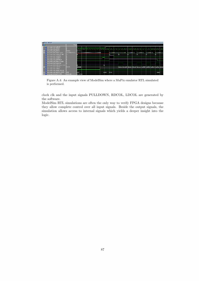
Figure A.4: An example view of ModelSim where a MuPix emulator RTL simulatedis performed.
clock clk and the input signals PULLDOWN, RDCOL, LDCOL are generated bythe software.ModelSim RTL simulations are often the only way to verify FPGA designs becausethey allow complete control over all input signals. Beside the output signals, thesimulation allows access to internal signals which yields a deeper insight into thelogic.
87

A.3 Multi-Channel Results
used rx channels BER0,1,6 < 2.3 · 10−12
0,1,7 < 9.0 · 10−12
0,1,5 1.7 · 10−11 ± 6.2 · 10−12
0,1,4 < 1.0 · 10−11
0,1,3 < 9.8 · 10−12
0,1,2 < 8.1 · 10−12
0,2,5 1.9 · 10−12 ± 1.9 · 10−12
0,4,5 1.1 · 10−5 ± 5.5 · 10−9
0,2,3 < 1.0 · 10−11
0,2,4 < 1.0 · 10−11
0,3,4 < 9.3 · 10−12
1,3,4 < 1.0 · 10−11
2,3,4 < 9.4 · 10−12
1,2,3 < 8.5 · 10−12
6,1,3 < 9.5 · 10−12
6,1,2 < 7.0 · 10−12
6,2,3 < 9.3 · 10−12
6,3,4 < 7.2 · 10−12
6,4,5 2.2 · 10−8 ± 2.1 · 10−10
7,6,2,0 < 2.2 · 10−12
7,6,1,0 < 5.2 · 10−12
7,6,3,0 < 4.0 · 10−12
7,6,4,0 < 2.9 · 10−12
7,6,5,0 < 3.5 · 10−12
7,6,0,2,5 2.2 · 10−12 ± 1.3 · 10−12
7,6,0,2,4 < 5.4 · 10−13
0,1,2,3,4 6.2 · 10−14 ± 4.3 · 10−14
0,1,2,3,4 4.9 · 10−15 ± 1.7 · 10−15
0,1,2,3,5 2.0 · 10−14 ± 2.0 · 10−14
Table A.1: BER rates for selected setups with multiple receiving channels performedat 6.4 Gbps with 50 m cables. For all channels the same random number generatorwith the same seed were used, hence all the data are synchronous.
A.4 MuPix4 Emulator
The MuPix4 is a prototype chip for the final MuPix chip of the Mu3e pixel sub-detector. It is used to develop a telescope CITE-LENNERT. For telescope debugingand to test LVDS links between two FPGAs an FPGA based emulator was produced.
The firmware written for the Stratix V development board uses the HSMA andHSMB ports to simulate the data of a MuPix4 chip read-out by boards developedby DIRK-CITE. Four chips can be simulated at the same time on one single FPGA.The emulator follows the same protocol as the pixel sensor and generates randomlydistributed hits with slightly disordered Gray code timestamps. In addition, thecontrol of single address bits of single channels provides a good debug tool.
The read-out protocol works as described below:
88
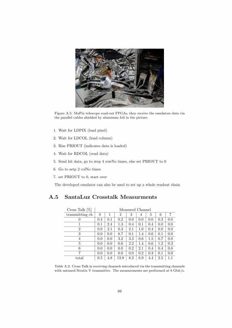
Figure A.5: MuPix telescope read-out FPGAs, they receive the emulators data viathe parallel cables shielded by aluminum foil in the picture.
1. Wait for LDPIX (load pixel)
2. Wait for LDCOL (load column)
3. Rise PRIOUT (indicates data is loaded)
4. Wait for RDCOL (read data)
5. Send hit data, go to step 4 rowNo times, else set PRIOUT to 0
6. Go to setp 2 colNo times
7. set PRIOUT to 0, start over
The developed emulator can also be used to set up a whole readout chain.
A.5 SantaLuz Crosstalk Measurments
Cross Talk [%] Measured Channeltransmitting ch 0 1 2 3 4 5 6 7
0 0.4 0.1 0.2 0.0 0.0 0.0 0.3 0.01 0.1 2.4 1.3 0.4 0.1 0.4 0.0 0.02 0.0 2.1 0.3 2.1 1.0 0.4 0.0 0.03 0.0 0.0 8.7 0.1 1.4 0.6 0.1 0.04 0.0 0.0 3.2 3.3 0.6 1.5 0.7 0.05 0.0 0.0 0.0 2.2 1.4 0.6 1.2 0.36 0.0 0.0 0.0 0.2 2.1 0.4 0.4 0.87 0.0 0.0 0.0 0.0 0.2 0.3 0.1 0.0
total 0.5 4.8 13.9 8.3 6.9 4.4 2.5 1.1
Table A.2: Cross Talk in receiving channels introduced via the transmitting channelswith untuned Stratix V transmitter. The measurements are performed at 8 Gbit/s.
89

Cross Talk [%] Measured Channeltransmitting ch 0 1 2 3 4 5 6 7
0 0.4 0.0 0.2 0.2 0.2 0.0 0.0 0.01 0.0 2.9 1.8 0.5 0.2 0.0 0.0 0.02 0.0 1.8 0.4 2.4 1.0 0.0 0.0 0.03 0.0 0.0 6.0 0.4 1.2 0.3 0.0 0.04 0.0 0.0 4.2 3.3 0.4 1.0 0.8 0.05 0.0 0.0 0.2 1.8 1.0 0.0 1.2 0.36 0.0 0.0 0.2 0.4 2.8 0.2 0.4 0.57 0.0 0.0 0.2 0.4 0.2 0.0 0.0 0.0
total 0.4 4.6 13.1 9.3 7.0 1.5 2.3 0.8
Table A.3: Cross Talk in receiving channels introduced via the transmitting channelswith tuned Stratix V transmitter. The measurements are performed at 8 Gbit/s.
Cross Talk [%] Measured Channelreceiving ch 0 1 2 3 4 5 6 7
0 - - 0.0 0.0 0.0 0.1 0.0 0.01 - - - 0.3 0.3 0.2 0.3 0.22 0.2 - - - 0.0 0.0 0.0 0.03 0.3 0.3 - - - 0.0 0.0 0.04 0.0 0.3 0.3 - - - 0.1 0.05 0.0 0.0 0.2 0.3 - - 1.0 0.16 0.0 0.0 0.0 0.2 0.3 1.2 - 1.27 0.0 0.0 0.1 0.0 0.3 0.2 0.3 -
Table A.4: Cross Talk in receiving channels introduced via the receiving channelswith Avago optical transmitter AFBR-57D7APZ. The measurements are performedat 8 Gbit/s and normalized to the 500 mV output signal stated in the specifications.
A.6 MuPix Address Scheme
90

A
A
A
A
FPGA Types:
A: 5x3 Chips with 3 Links: 45 Links 12 FPGAs
D: 4x9 Chips with 1 Link: 36 Links 26 FPGAs
Upstream side Downstream side
D
Upstream side Downstream side
D
D
D
D
D
D
D D
D
D
D
D
D
D
D
DD
D
D
D
D
D
D
D
D
Mu3e Phase I
Pixel Readout SchemeVertex Layers
Outer Layers
v1 2.10.2013 NB
v2 21.10.2013 NB
v3 24.2.2014 NB
All addresses in hexadicemal notation
0
1
4
8
9
5
0
1
2
45
9
A
D
C
1011
12
14
15
16
01
2
3
4
5
6
7
8
9
A
B
01
2
3
4
5
6
7
8
9
A
BCD
E
F
10
11
12
13
14
15
1617
C
DE
F
10
11
12
13
14
15
16
17
18
19
1A
1B0
1
2
3
4
5
6
7
8
9
A
B
01
2
3
4
5
6
7
8
9
A
BC D
E
F
10
11
12
13
14
15
1617
CD
E F
10
11
12
13
14
15
16
17
18
19
1A
1B
Upstream Downstreamz
4 5 61 2 3
0 1 2 0 1 2 0 1 2 0 1 2 0 1 2 0 1 2
Chip
Link
0 0
11
2 2
33
Upstream Downstreamz
Chip
Link
10 11 12 13 14 15 16 17 18E FC DA B8 97
0 0 0 0 0 0 0 0 0 0 0 0 0 0 0 0 0 0
Address Scheme:
Inner Layers:
Outer Layers:
Ro
w
8(7) bit8 bit
Co
l
Ch
ip
3P
hi
5
La
yer
0 0 0
4(1)
28 bit
Ro
w
8 bit8 bit
Co
l
Ch
ip
5
Ph
i
5
La
yer
0 0 1
4(1)
30 bit
0
A
A
6
8
E
C
D
1011
14
15
A
A
A
A
0
1
4
8
9
5
0
1
2
45
9
A
D
C
1011
12
14
15
16
A
A
6
8
E
C
D
10 11
14
15

List of Figures
1.1 Standard Model . . . . . . . . . . . . . . . . . . . . . . . . . . . . . . 31.2 Feynman diagram µ decay via neutrino mixing . . . . . . . . . . . . 41.4 History of LFV measurements. . . . . . . . . . . . . . . . . . . . . . 51.5 Mu3e experiment setup. . . . . . . . . . . . . . . . . . . . . . . . . . 71.6 Mu3e detector randering . . . . . . . . . . . . . . . . . . . . . . . . . 91.7 Readout Scheme . . . . . . . . . . . . . . . . . . . . . . . . . . . . . 101.8 Readout scheme with multiplicities . . . . . . . . . . . . . . . . . . . 11
2.1 Self-synchronizing scrambler . . . . . . . . . . . . . . . . . . . . . . . 192.2 Interlaken protocol overview . . . . . . . . . . . . . . . . . . . . . . . 212.3 Eye Diagram . . . . . . . . . . . . . . . . . . . . . . . . . . . . . . . 242.4 BERT bathtub plots . . . . . . . . . . . . . . . . . . . . . . . . . . . 24
3.1 Flip-Flop . . . . . . . . . . . . . . . . . . . . . . . . . . . . . . . . . 283.2 Block diagram of the basic PLL concept. . . . . . . . . . . . . . . . . 29
4.1 FPGA architecture . . . . . . . . . . . . . . . . . . . . . . . . . . . . 32
5.1 Stratix V architecture . . . . . . . . . . . . . . . . . . . . . . . . . . 355.2 Stratix V Development Board . . . . . . . . . . . . . . . . . . . . . . 365.3 SantaLuz Mezzanin Board . . . . . . . . . . . . . . . . . . . . . . . . 385.4 Electrical SFP . . . . . . . . . . . . . . . . . . . . . . . . . . . . . . 385.5 Optical SFP . . . . . . . . . . . . . . . . . . . . . . . . . . . . . . . . 385.6 Transceiver State Machine . . . . . . . . . . . . . . . . . . . . . . . . 415.7 BERT flow diagram . . . . . . . . . . . . . . . . . . . . . . . . . . . 435.8 Eye diagrams with different analog tune values . . . . . . . . . . . . 455.9 EyeQ diagram in the transceiver toolkit. . . . . . . . . . . . . . . . . 465.10 Optical link verification base setup . . . . . . . . . . . . . . . . . . . 495.11 Single channel single board optical SFP setup. . . . . . . . . . . . . 505.12 BER vs rate . . . . . . . . . . . . . . . . . . . . . . . . . . . . . . . . 515.13 Number of tolerated zeros in a row. . . . . . . . . . . . . . . . . . . . 525.14 Setup to test different cages . . . . . . . . . . . . . . . . . . . . . . . 535.15 Cage performance . . . . . . . . . . . . . . . . . . . . . . . . . . . . 545.16 Single channel multi-board optical SFP setup. . . . . . . . . . . . . . 545.17 Crosstalk . . . . . . . . . . . . . . . . . . . . . . . . . . . . . . . . . 565.18 Setup for analog tuned transceivers. . . . . . . . . . . . . . . . . . . 565.19 Running disparity of different data patterns. . . . . . . . . . . . . . . 59
6.1 Front-End sorting concepts. . . . . . . . . . . . . . . . . . . . . . . . 67
92
6.2 Coordinate transformation on FPGA simulation. . . . . . . . . . . . 69
7.1 LVDS impedance . . . . . . . . . . . . . . . . . . . . . . . . . . . . . 727.2 50 nm Al structures on 25 µm Kapton film. . . . . . . . . . . . . . . 737.3 25 µm Al structures on 25 µm Kapton film. . . . . . . . . . . . . . . 73
8.1 Proposed phase Ia readout chain . . . . . . . . . . . . . . . . . . . . 79
A.1 PMA overview . . . . . . . . . . . . . . . . . . . . . . . . . . . . . . 80A.2 Stratix V Standard PCS overview. . . . . . . . . . . . . . . . . . . . 82A.3 Stratix V 10G PCS overview. . . . . . . . . . . . . . . . . . . . . . . 84A.4 ModelSim example view . . . . . . . . . . . . . . . . . . . . . . . . . 87A.5 MuPix Telescope read-our FPGAs . . . . . . . . . . . . . . . . . . . 89
93

List of Tables
2.1 5b/6b encoding . . . . . . . . . . . . . . . . . . . . . . . . . . . . . . 172.2 3b/4b encoding . . . . . . . . . . . . . . . . . . . . . . . . . . . . . . 182.3 Structure of a Interlaken idle/burst word. . . . . . . . . . . . . . . . 222.4 CRC example. . . . . . . . . . . . . . . . . . . . . . . . . . . . . . . 25
3.1 Simplest logic gates with their symbols. . . . . . . . . . . . . . . . . 27
5.1 Stratix V (5SGSMD5K2F40C2N) specifications. . . . . . . . . . . . . 345.2 Analog SFP tune values. . . . . . . . . . . . . . . . . . . . . . . . . . 575.3 8.0 Gbit/s SFP and 11.3 Gbit/s QSFP loopback measurments. . . . 585.4 8.0 Gbit/s BER with analog tuned transceivers . . . . . . . . . . . . 605.5 6.4 Gbit/s BER with analog tuned transceivers . . . . . . . . . . . . 615.6 QSFP BERs . . . . . . . . . . . . . . . . . . . . . . . . . . . . . . . . 615.7 Analog QSFP tune values . . . . . . . . . . . . . . . . . . . . . . . . 625.8 Optical transmission BER overview . . . . . . . . . . . . . . . . . . . 62
6.1 Fmax for different coordinate tranfo implementations. . . . . . . . . 70
7.1 Laser cutter values. . . . . . . . . . . . . . . . . . . . . . . . . . . . . 747.2 Minimal aluminum scales . . . . . . . . . . . . . . . . . . . . . . . . 75
A.1 BER of multi-channel setup. . . . . . . . . . . . . . . . . . . . . . . . 88A.2 Cross Talk in receiving channels introduced via the transmitting chan-
nels with untuned Stratix V transmitter. The measurements are per-formed at 8 Gbit/s. . . . . . . . . . . . . . . . . . . . . . . . . . . . . 89
A.3 Cross Talk in receiving channels introduced via the transmitting chan-nels with tuned Stratix V transmitter. The measurements are per-formed at 8 Gbit/s. . . . . . . . . . . . . . . . . . . . . . . . . . . . . 90
A.4 Cross Talk in receiving channels introduced via the receiving channelswith Avago optical transmitter AFBR-57D7APZ. The measurementsare performed at 8 Gbit/s and normalized to the 500 mV output signalstated in the specifications. . . . . . . . . . . . . . . . . . . . . . . . 90
94

Bibliography
[1] CMS Collaboration. Observation of a new boson at a mass of 125 GeV withthe CMS experiment at the LHC. Physics Letters B, 716, 2012.
[2] Barry R. Holstein John F. Donoghue, Eugene Golowich. Dynamics of theStandard Model. Cambridge : Cambridge University Press, 1992.
[3] C.P. Burgess and Guy D. Moore. The standard model : a primer. Cambridge: Cambridge University Press, 2007.
[4] Wikimedia Commons. Standard model of elementary particles, 2014. [Online;accessed 10-februar-2014].
[5] Y. Fukuda et al. Evidence for oscillation of atmospheric neutrinos. Phys. Rev.Lett., 81:1562–1567, 1998.
[6] Q. R. Ahmad et al. Measurement of the charged current interactions producedby B-8 solar neutrinos at the Sudbury Neutrino Observatory. Phys. Rev. Lett.,87:071301, 2001.
[7] K. Eguchi et al. First results from KamLAND: Evidence for reactor anti-neutrino disappearance. Phys. Rev. Lett., 90:021802, 2003.
[8] K. Nakamu and S.T. Petcov (DPG). Update: Neutrino mass, mixing, andoscillations. DPG, May 2013.
[9] Laurent Canetti and Mikhail Shaposhnikov. The ν MSM and muon to electronconversion experiments. Hyperfine Interact., 214(1-3):5–11, 2013.
[10] L. Maiani S.L. Glashow, J. Iliopoulos. Weak interactions with lepton–hadronsymmetry. Physical Review D, 2, 1970.
[11] A. Blondel et al. Research Proposal for an Experiment to Search for the Decayµ→ eee. ArXiv e-prints, January 2013.
[12] W. J. Marciano, T. Mori, and J. M. Roney. Charged Lepton Flavor ViolationExperiments. Ann.Rev.Nucl.Part.Sci., 58:315–341, 2008.
[13] U. Bellgardt et al. Search for the Decay µ+ → e+e+e−. Nucl.Phys., B299:1,1988.
[14] W. Ootani. New results from MEG experiment. pages 475–480, 2013.
95

[15] J.L. Hewett, H. Weerts, K.S. Babu, J. Butler, B. Casey, et al. Planningthe Future of U.S. Particle Physics (Snowmass 2013): Chapter 2: IntensityFrontier. 2014.
[16] K. Nakamura et al. Review of particle physics. J. Phys., G37:075021, 2010.
[17] I. Peric et al. High-voltage pixel detectors in commercial CMOS technologiesfor ATLAS, CLIC and Mu3e experiments. Nucl.Instrum.Meth., A731:131–136,2013.
[18] A.-K. Perrevoort. Characterisation of high voltage monolithic active pixelsensors for the mu3e experiment. Master’s thesis, Heidelberg University, 2012.
[19] H. Augustin. Charakterisierung von HV-MAPS. Master’s thesis, HeidelbergUniversity, 2012.
[20] A. Damyanova. Development of a Scintillating Fibre Tracker/Time-of-FlightDetector with SiPM Readout for the Mu3e Experiment at PSI. Master’s thesis,Geneva University, 2013.
[21] Carlo Licciulli. [prazise zeitmessung fur das mu3e-experiment. Master’s thesis.
[22] Patrick Eckert. PhD thesis, Kirchhoff Institut fur Physik. Personal contact.
[23] Lukas Huxold. Cooling of the Mu3e Pixel Detector, 2014.
[24] Fabian Forster. Master’s thesis, University of Heidelberg, 2014. Personalcontact.
[25] S. Bachmann et al. The proposed trigger-less TBit/s readout for the Mu3eexperiment. Jinst, (9), January 2014.
[26] Niklaus Berger. Read-out simulation. In Mu3e internal notes, November 2013.
[27] Gianfranco Cariolaro. Unified signal theory. London : Springer, 2011.
[28] John David Jackson. Classical Electrodynamics. John Wiley & Sons, Inc., NewJersey, USA, 3 edition, 1991.
[29] Return-to-zero coding in optical intersatellite links. Technische UniversitatWien, 2003.
[30] R Forster. Manchester encoding: Opposing definitions resolved. EngineeringScience & Education Journal, 200.
[31] Jianfeng Zhang, P.V. Holm-Nielsen Nan Chi, C. Peucheret, and P. Jeppesen.10 Gbit/s Menchester-encoded FSK-labelled optical signal transmission linkS.Electronics Letters Online, (20030769), April 2003.
[32] Dennis Derickson; Marcus Muller. Digital Communications Test and Measure-ment: High-Speed Physical Layer Characterization. Prentice Hall, December2007.
[33] P. A. Franaszek A. X. Widmer. A dc-balanced, partitioned-block, 8b/10btransmission code. IBM Journal of Research and Development, 27(5):440,1983.
96

[34] Byte oriented dc balanced (0,4) 8b/10b partitioned block transmission code,1984.
[35] Patent: 64b/66b decoding, for packetized serial data, 2001.
[36] Bijan Raahemi. ERROR CORRECTION ON 64/66 BIT ENCODED LINKS.University of Ottawa, May 2005.
[37] Robert Melancton Metcalfe. Packet Communication. Cambridge : Mas-sachusetts Inst. of Tech., 1973.
[38] IEEE: Ethernet 802.3.
[39] G. Held. Ethernet Networks: Design, Implementation, Operation, Manage-ment. Wiley professional computing. Wiley, 2003.
[40] IEEE: 10GE 802.3e.
[41] IEEE-802.3 Clause 49, 64b/66b.
[42] Amendment: Media Access Control (MAC) Parameters, Phzsical LLayer, andManagement Parameters for 10 Gbps Operation.
[43] System Packet Interface Level 4 (SPI-4) Phase 2 Revision 1: OC-192 SystemInterface for Physical and Link Layer Devices.
[44] Interlaken protocol definition, October 7, 2008.
[45] Understanding data eye diagram methodology for analyzing high speed digitalsignals. ON Semiconductors, AND9075/D.
[46] WAVECREST Corporation. Relationship Between Eye Diagram and BathtubCurves, 2003.
[47] Agilent Technologies. Measuring Jitter in Difital Systems Application Note,2013.
[48] Martin Stigge, Henryk Ploetz, Wolf Mueller, and Jens-Peter Redlich. Reversingcrc - theory and practice. HU Berlin Public Report, 2006.
[49] MIT 6.02. LECTURE 7: Detecting Bit Errors. 2010.
[50] Philip Koopman and ridib Chakravarty. The International Conference on De-pendable Systems and Networks. 2004.
[51] Philip Koopman. The International Conference on Dependable Systems andNetworks. In 32-Bit Cyclic Redundancy Codes for Internet Applications, 2002.
[52] Justin S. Davis Robert B. Reese (Robert Bryan). Finite state machine datapathdesign, optimization, and implementation. 2008.
[53] D.J. McElroy. High density floating gate electrically programmable rom, Jan-uary 15 1980. US Patent 4,184,207.
[54] Nikolaos I. Margaris. Theory of the Non-linear Analog Phase Locked Loop(Lecture Notes in Control and Information Sciences). Springer, 2004.
97

[55] Tom A. D. Riley, Miles A. Copeland, and Tad A. Kwasniewski. Delta-sigmamodulation in fractional-n frequency synthesis. IEEE Jurnal of Solid StateCircuits, 28(5):553–559, May 1993.
[56] Altera. Stratix V Device Handbook Volume 2: Transceivers, 2013.05.06 edition,May 2013.
[57] Makoto Murase. Linear feedback shift register, 1992.
[58] Tim Molteno Roy Ward. Table of Linear Feedback Shift Registers. Departmentof Physics, University of Otago, Box 56, Dunedin, New Zealand, October 2007.
[59] Xilinx. Efficient Shift Registers, LFSR Counters, and Long Pseudo-RandomSequence Generators, 1.1 edition, July 1996. XAPP 052.
[60] Megan Dewar and Brett Stevens. Ordering Block Designs: Gray Codes,Universal Cycles and Configuration Orderings (CMS Books in Mathematics).Springer, 2012.
[61] FPGA-based Implementation of Signal Processing Systems. Wiley, 2008.
[62] J. Rose, A. E. Gamal, , and A. Sangiovanni-Vincentelli. Architecture of field-programmable gate arrays. Proceedings of the IEEE, 81(7):1013 – 1029, 1993.
[63] Altera Homepage, January 2014.
[64] Altera. Reducing Power Consumption and Increasing Bandwidth on 28-nmFPGAs, wp-01148-2.0 edition, March 2012.
[65] Altera. Logic Array Blocks and Adaptive Logic Modules in Stratix V Devices,2014.01.10 edition, January 2014.
[66] Altera Homepage: DSP, February 2014.
[67] Altera. White Paper: Enabling High-Performance DSP Applications withStratix V Variable-Precision DSP Blocks, 1.1 edition, May 2011.
[68] Altera. Embedded Memory Blocks in Stratix V Devices, 2013.05.06 edition,May 2013.
[69] Altera. Stratix V Device Overview, 2014.01.10 edition, January 2014.
[70] Altera. High Speed Mezzanine Card (HSMC), 1.7 edition, June 2009.
[71] QSFP+ 10 Gb/s 4X Pluggable Transceiver Solution (QSFP10). SFF Commit-tee Specification , 2013.
[72] Altera. Stratix V GX FPGA Development Board Reference Manual, 1.3 edi-tion, July 2012.
[73] Helmholtz Alliance. Ha-101 physics at the terascale. Annual Report 2011,2012.
[74] Christian Farber. PhD thesis, 2013. Personal contact.
[75] C. Grzesik. Fast Optical Readout for the Mu3e Experiment, 2014.
98

[76] INF-8074i Specification for SFP (Small Formfactor Pluggable) Transceiver,May 2001.
[77] SFF-8431 Specification for SFP+, July 2009.
[78] TrioFlex. Online Catalog, January 2014.
[79] Avago Technologies. AFBR-57D7APZ Data Sheet, January 2013.
[80] HQDP Series 228.6 mm Cable Length Signal Integrity Performance. Technicalreport, Samtec.
[81] Molex. Datasheet: 106410-1003, September 2013.
[82] Molex. Online: QSFP+ Interconnect, January 2013.
[83] Robert Czerwinski Dariusz Kania. Finite state machine logic synthesis forcomplex programmable logic devices. 2013.
[84] Ransom Stephens. PRBS31: Slower, costlier, worse. EDN Network, 2012.
[85] Ilya Narsky. Estimation of upper limits using a poisson statistic. arXiv:hep-ex/9904025, page 24, 1999.
[86] T. Bayes. Facsimiles of Two Papers by Bayes. Hafner Publ. Co., 1963.
[87] P.S. Laplace. Philosophical Essay on Probabilities. Dover Publications, 1951.
[88] Altera. Floating-Point Megafunction, 7.0 edition, November 2012.
[89] DuPoint. DuPoint Kapton: General Specifications, March 2012.
[90] DuPoint. DuPoint Kapton: Summery of Properties.
[91] X.-F. Navick, M. Carty, G. Chapellier, M.and Chardin, C. Goldbach,R. Granelli, S. Herve, and M. et al. Karolak. Fabrication of ultra-low ra-dioactivity detector holders for Edelweiss-II. NIM, 520:189–192, 2004.
[92] Universal Laser System. PL6MW Platform.
[93] M. Baranek J. Bartl. Emissivity of aluminium and its importance for radio-metric measurement. Measurement of Physical Quantities, 4:31–36, 2004.
[94] Avago Technologies. MicroPOD AFBR-77D4SZ, AFBR-78D4SZ, March 2013.
[95] Cisco. Cisco 40GBASE QSFP Modules, 2014.
[96] Altera. Dynamic Reconfiguration in Stratix V Devices, 2013.05.06 edition, May2013.
[97] Altera. Extending Transceiver Leadership at 28 nm, 2.1 edition, October 2012.
[98] Altera. Using the On-Chip Signal Quality Monitoring Circuitry (EyeQ) Featurein Stratix IV Transceivers, 1.2 edition, September 2010.
[99] Altera. Debugging Transceiver Links, 13.1.0 edition, November 2013.
[100] Altera. Avalon Streaming Data Pattern Generator and Checker Cores, v9.1.1edition, January 2010.
99

Acknowledgements
I would like to express my thanks to everyone that accompanied me during mytime in the Mu3e group in Heidelberg. It was always a pleasure to work in such aatmosphere.
First of all, I would like to thank Dr. Niklaus Berger who made it possible tocarry out a thesis in Heidelbergd and for his support during the whole time. Myspecial thanks goes to Dr. Dirk Wiedner for his help, support and discussions.
I thank Carsten Grzesik with whom I carried out most of the work. Numerousjoint discussions have brought us a long way.
Last but not least, I would like to thank Prof. Dr. Gunther Dissertori who sup-ported the idea of this ETH thesis at the University of Heidelberg from the begin-ning.
100


