Embed Size (px)
Citation preview

V up to 70 VFAULT
M0092-01
Product
Folder
Sample &Buy
Technical
Documents
Tools &
Software
Support &Community
SN65HVD1785, SN65HVD1786, SN65HVD1787SN65HVD1791, SN65HVD1792, SN65HVD1793
SLLS872I –JANUARY 2008–REVISED AUGUST 2015
SN65HVD17xx Fault-Protected RS-485 Transceivers With Extended Common-Mode Range1 Features 3 Description
These devices are designed to survive overvoltage1• Bus-Pin Fault Protection to:
faults such as direct shorts to power supplies, mis-– > ±70 V ('HVD1785, 86, 91, 92) wiring faults, connector failures, cable crushes, and– > ±30 V ('HVD1787, 93) tool mis-applications. They are also robust to ESD
events, with high levels of protection to human-body• Common-Mode Voltage Range (–20 V to 25 V)model specifications.More Than Doubles TIA/EIA 485 RequirementThese devices combine a differential driver and a• Bus I/O Protectiondifferential receiver, which operate from a single– ±16 kV JEDEC HBM Protectionpower supply. In the 'HVD1785, 'HVD1786, and
• Reduced Unit Load for Up to 256 Nodes 'HVD1787, the driver differential outputs and the• Failsafe Receiver for Open-Circuit, Short-Circuit receiver differential inputs are connected internally to
form a bus port suitable for half-duplex (two-wire bus)and Idle-Bus Conditionscommunication. In the 'HVD1793, the driver• Low Power Consumptiondifferential outputs and the receiver differential inputs
– Low Standby Supply Current, 1 μA Typical are separate pins, to form a bus port suitable for full-– ICC 5 mA Quiescent During Operation duplex (four-wire bus) communication. These ports
feature a wide common-mode voltage range, making• Power-Up, Power-Down Glitch-Free Operationthe devices suitable for multipoint applications overlong cable runs. These devices are characterized2 Applicationsfrom –40°C to 105°C.
• Designed for RS-485 and RS-422 NetworksFor similar features with 3.3-V supply operation, seethe SN65HVD1781 (SLLS877).
Device Information(1)
PART NUMBER PACKAGE BODY SIZE (NOM)SN65HVD1785, SOIC (8) 4.90 mm × 3.91 mmSN65HVD1786,
PDIP (8) 9.81 mm × 6.35 mmSN65HVD1787SN65HVD1791,SN65HVD1792, SOIC (14) 8.65 mm × 3.91 mmSN65HVD1793
(1) For all available packages, see the orderable addendum atthe end of the datasheet.
Example of Bus Short to Power Supply
1
An IMPORTANT NOTICE at the end of this data sheet addresses availability, warranty, changes, use in safety-critical applications,intellectual property matters and other important disclaimers. PRODUCTION DATA.

SN65HVD1785, SN65HVD1786, SN65HVD1787SN65HVD1791, SN65HVD1792, SN65HVD1793SLLS872I –JANUARY 2008–REVISED AUGUST 2015 www.ti.com
Table of Contents9.2 Functional Block Diagram ....................................... 151 Features .................................................................. 19.3 Feature Description................................................. 152 Applications ........................................................... 19.4 Device Functional Modes........................................ 183 Description ............................................................. 1
10 Application and Implementation........................ 194 Revision History..................................................... 210.1 Application Information.......................................... 195 Product Selection Guide ....................................... 410.2 Typical Application ............................................... 196 Pin Configuration and Functions ......................... 4
11 Power Supply Recommendations ..................... 217 Specifications......................................................... 512 Layout................................................................... 227.1 Absolute Maximum Ratings ..................................... 5
12.1 Layout Guidelines ................................................. 227.2 ESD Ratings.............................................................. 612.2 Layout Example .................................................... 227.3 Recommended Operating Conditions....................... 6
13 Device and Documentation Support ................. 237.4 Thermal Information .................................................. 613.1 Documentation Support ........................................ 237.5 Electrical Characteristics........................................... 713.2 Related Links ........................................................ 237.6 Thermal Considerations ............................................ 813.3 Community Resources.......................................... 247.7 Switching Characteristics .......................................... 813.4 Trademarks ........................................................... 247.8 Typical Characteristics ............................................ 1013.5 Electrostatic Discharge Caution............................ 248 Parameter Measurement Information ................ 1113.6 Glossary ................................................................ 249 Detailed Description ............................................ 15
14 Mechanical, Packaging, and Orderable9.1 Overview ................................................................. 15 Information ........................................................... 24
4 Revision HistoryNOTE: Page numbers for previous revisions may differ from page numbers in the current version.
Changes from Revision H (February 2010) to Revision I Page
• Added Pin Configuration and Functions section, ESD Ratings table, Feature Description section, Device FunctionalModes, Application and Implementation section, Power Supply Recommendations section, Layout section, Deviceand Documentation Support section, and Mechanical, Packaging, and Orderable Information section .............................. 1
Changes from Revision G (April 2009) to Revision H Page
• Deleted 70-V from the data sheet title.................................................................................................................................... 1• Changed first Features Bullet From: Bus-Pin Fault Protection to > ±70 V To: Bus-Pin Fault Protection to: > ±70 V
('HVD1785, 86,91,92), > ±30 V ('HVD1787, 93)..................................................................................................................... 1• Changed Voltage range at A and B inputs in the ABS MAX RATINGS table, adding seperate conditions for the
different devices...................................................................................................................................................................... 5• Changed From: Voltage input range, transient pulse, A and B, through 100 Ω To: Transient overvoltage pulse
through 100 Ω per TIA-485..................................................................................................................................................... 5• Added the 70-V Fault-Protection section.............................................................................................................................. 16
Changes from Revision F (November 2008) to Revision G Page
• Added IOH = –400 μA conditions and values to the Receiver high-level output voltage ........................................................ 7• Added Receiver enabled VCM > VCC ...................................................................................................................................... 8• Added Receiver Failsafe information.................................................................................................................................... 15• Changed the Receiver Failsafe section................................................................................................................................ 16
2 Submit Documentation Feedback Copyright © 2008–2015, Texas Instruments Incorporated
Product Folder Links: SN65HVD1785 SN65HVD1786 SN65HVD1787 SN65HVD1791 SN65HVD1792 SN65HVD1793

SN65HVD1785, SN65HVD1786, SN65HVD1787SN65HVD1791, SN65HVD1792, SN65HVD1793
www.ti.com SLLS872I –JANUARY 2008–REVISED AUGUST 2015
Changes from Revision E (July 2008) to Revision F Page
• Added to Title: With Extended Common-Mode Range .......................................................................................................... 1• Added Receiver enabled VCM > VCC condition and values to the Driver enabled time ......................................................... 8• Added Figure 4 .................................................................................................................................................................... 10
Changes from Revision D (June 2008) to Revision E Page
• Changed - Removed Product Preview label .......................................................................................................................... 4• Changed SN65HVD1792 Removed Product Preview label ................................................................................................... 4• Changed SN65HVD1793 Removed Product Preview label ................................................................................................... 4
Changes from Revision C (March 2008) to Revision D Page
• Added Features Bullet: Power-Up, Power-Down Glitch-Free Operation................................................................................ 1• Changed (Preview) to part number SN65HVD1791 in the Product Selection Guide............................................................. 4• Added section - APPLICATION INFORMATION.................................................................................................................. 15• Changed Receiver disabled by default - Enable from X to OPEN. Output from OPEN to Z ............................................... 18
Changes from Revision B (March 2008) to Revision C Page
• Changed Rec Op Table. Signaling rate, HVD1787, HVD1793 From: 20 Mbps max to 10 Mbps max. ................................. 6
Changes from Revision A (March 2008) to Revision B Page
• Added TA ≤ 85°C and TA ≤ 105°C conditions and values to the Receiver low-level output voltage. ..................................... 7• Changed the max value for Supply Current (quiescent) Driver and receiver disabled, From 1 μA To 5 μA. ........................ 7
Changes from Original (January 2008) to Revision A Page
• Changed Features Bullet From: Low Standby Supply Current, 2 μA Max To: Low Standby Supply Current, 1 μA Typ....... 1• Deleted columns to the PRODUCT SELECTION GUIDE for Package Options and Status.................................................. 4• Added text: For similar features with 3.3 V supply operation... .............................................................................................. 4• Changed the Product Selection Guide Signaling Rate for SN65HVD1787 From 20 Mbps To: 10 Mbps.............................. 4• Changed the Product Selection Guide Signaling Rate for SN65HVD1793 From 20 Mbps To: 10 Mbps.............................. 4• Deleted The Competitive Comparison table........................................................................................................................... 5• Added |VOD| RS-485 with common-mode load TA ≤ 85°C and TA ≤ 105°C............................................................................ 7• Changed ΔVOC From min = -0.2 mV and max 0.2 mV To: min = -100 mV and max 100 mV ............................................... 7• Changed HVD1785/1791 Driver differential output rise/fall time max value From 2.5 μs To: 2.6 μs. ................................... 8• Changed HVD1787/1793 Driver differential output rise/fall time max value From 1.5 ns To: 30 ns...................................... 8• Changed Receiver propagation delay max value From 50 ns To: 70 ns. .............................................................................. 9• Changed tPLZ, tPHZ Receiver disable time From 3000 ns To 100 ns....................................................................................... 9• Deleted graph DIFFERENTIAL OUTPUT VOLTAGE vs DIFFERENTIAL LOAD CURRENT.............................................. 10
Copyright © 2008–2015, Texas Instruments Incorporated Submit Documentation Feedback 3
Product Folder Links: SN65HVD1785 SN65HVD1786 SN65HVD1787 SN65HVD1791 SN65HVD1792 SN65HVD1793

R
RE
DE
D
VCC
B
A
GND
1
2
3
4
8
7
6
5
SN65HVD1785, SN65HVD1786, SN65HVD1787SN65HVD1791, SN65HVD1792, SN65HVD1793SLLS872I –JANUARY 2008–REVISED AUGUST 2015 www.ti.com
5 Product Selection Guide
PART NUMBER DUPLEX SIGNALING RATE NODES CABLE LENGTH
SN65HVD1785 Half 115 kbps Up to 256 1500 m
SN65HVD1786 Half 1 Mbps Up to 256 150 m
SN65HVD1787 Half 10 Mbps Up to 64 50 m
SN65HVD1791 Full 115 kbps Up to 256 1500 m
SN65HVD1792 Full 1 Mbps Up to 256 150 m
SN65HVD1793 Full 10 Mbps Up to 64 50 m
6 Pin Configuration and Functions
D or P Package8-Pin SOIC or PDIP
SN65HVD1785, 1786, 1787 Top View
Pin Functions (SN65HVD1785, SN65HVD1786, SN65HVD1787)PIN
TYPE DESCRIPTIONNAME NO.
BusA 6 Driver output or receiver input (complementary to B)input/outputBusB 7 Driver output or receiver input (complementary to A)input/output
D 4 Digital input Driver data inputDE 3 Digital input Driver enable, active high
ReferenceGND 5 Local device groundpotentialR 1 Digital output Receive data outputRE 2 Digital input Receiver enable, active lowVCC 8 Supply 4.5-V-to-5.5-V supply
4 Submit Documentation Feedback Copyright © 2008–2015, Texas Instruments Incorporated
Product Folder Links: SN65HVD1785 SN65HVD1786 SN65HVD1787 SN65HVD1791 SN65HVD1792 SN65HVD1793

1
2
3
4
5
6
7
14
13
12
11
10
9
8
NC
GND
GND
Z
Y
NC
R
RE
DE
D
VCC
VCC
A
B
SN65HVD1785, SN65HVD1786, SN65HVD1787SN65HVD1791, SN65HVD1792, SN65HVD1793
www.ti.com SLLS872I –JANUARY 2008–REVISED AUGUST 2015
D Package14-Pin SOIC
SN65VD1791, 1792, 1793 Top View
NC - No internal connectionPins 6 and 7 are connected together internally.Pins 13 and 14 are connected together internally.
Pin Functions (SN65HVD1791, SN65HVD1792, SN65HVD1793)PIN
TYPE DESCRIPTIONNAME NO.A 12 Bus input Receiver input (complementary to B)B 11 Bus input Receiver input (complementary to A)Y 9 Bus output Driver output (complementary to Z)Z 10 Bus output Driver output (complementary to Y)D 5 Digital input Driver data inputDE 4 Digital input Driver enable, active high
ReferenceGND 6, 7 Local device groundpotentialR 2 Digital output Receive data outputRE 3 Digital input Receiver enable, active lowVCC 13, 14 Supply 4.5-V to 5.5-V supplyNC 1, 8 No connect No connect; should be left floating
7 Specifications
7.1 Absolute Maximum Ratings (1)
MIN MAX UNITVCC Supply voltage –0.5 7 V
'HVD1785, 86, 91, 92, 93 A, B pins –70 70 VVoltage at bus pins 'HVD1787 A, B pins –70 30 V
'HVD1793 Y, Z pins –70 30 VInput voltage at any logic pin –0.3 VCC + 0.3 VTransient overvoltage pulse through 100 Ω per TIA-485 –100 100 VReceiver output current –24 24 mA
TJ Junction temperature 170 °CTstg Storage temperature 160 °C
(1) Stresses beyond those listed under Absolute Maximum Ratings may cause permanent damage to the device. These are stress ratingsonly and functional operation of the device at these or any other conditions beyond those indicated under Recommended OperatingConditions is not implied. Exposure to absolute-maximum-rated conditions for extended periods may affect device reliability.
Copyright © 2008–2015, Texas Instruments Incorporated Submit Documentation Feedback 5
Product Folder Links: SN65HVD1785 SN65HVD1786 SN65HVD1787 SN65HVD1791 SN65HVD1792 SN65HVD1793

SN65HVD1785, SN65HVD1786, SN65HVD1787SN65HVD1791, SN65HVD1792, SN65HVD1793SLLS872I –JANUARY 2008–REVISED AUGUST 2015 www.ti.com
7.2 ESD RatingsVALUE UNIT
Human body model (HBM), per ANSI/ESDA/JEDEC JS-001 (1), Bus terminals and GND ±16000JEDEC Standard 22, Test Method A114 All pins ±4000
Electrostatic Charged-device model (CDM), per JEDEC specification JESD22-C101 (2),V(ESD) ±2000 Vdischarge JEDEC Standard 22, Test Method C101Machine Model, JEDEC Standard 22, Test Method A115 ±400IEC 60749-26 ESD (human-body model) Bus terminals and GND ±16000
(1) JEDEC document JEP155 states that 500-V HBM allows safe manufacturing with a standard ESD control process.(2) JEDEC document JEP157 states that 250-V CDM allows safe manufacturing with a standard ESD control process.
7.3 Recommended Operating ConditionsMIN NOM MAX UNIT
VCC Supply voltage 4.5 5 5.5 VVI Input voltage at any bus terminal (separately or common mode) (1) –20 25 VVIH High-level input voltage (driver, driver enable, and receiver enable inputs) 2 VCC VVIL Low-level input voltage (driver, driver enable, and receiver enable inputs) 0 0.8 VVID Differential input voltage –25 25 V
Output current, driver –60 60 mAIO Output current, receiver –8 8 mARL Differential load resistance 54 60 ΩCL Differential load capacitance 50 pF
HVD1785, HVD1791 115 kbps1/tUI Signaling rate HVD1786, HVD1792 1
MbpsHVD1787, HVD1793 10
TA Operating free-air temperature (see application section for thermal information) –40 105 °CTJ Junction temperature –40 150 °C
(1) By convention, the least positive (most negative) limit is designated as minimum in this data sheet.
7.4 Thermal InformationSN65HVD1791,SN65HVD1785, SN65HVD1786, SN65HVD1792,
SN65HVD1787 SN65HVD1793THERMAL METRIC (1) UNITD (SOIC) P (PDIP) D (SOIC)8 PINS 8 PINS 14 PINS
RθJA Junction-to-ambient thermal resistance 138 59 95 °C/WRθJA (low-K) Junction-to-case (top) thermal resistance 242 128 168 °C/WRθJC(top) Junction-to-board thermal resistance 61 61 44 °C/WRθJB Junction-to-top characterization parameter 62 39 40 °C/WψJT Junction-to-board characterization parameter 3.4 17.6 8.2 °C/WψJB Junction-to-case (bottom) thermal resistance 33.4 28.3 25 °C/W
(1) For more information about traditional and new thermal metrics, see the Semiconductor and IC Package Thermal Metrics applicationreport, SPRA953.
6 Submit Documentation Feedback Copyright © 2008–2015, Texas Instruments Incorporated
Product Folder Links: SN65HVD1785 SN65HVD1786 SN65HVD1787 SN65HVD1791 SN65HVD1792 SN65HVD1793
SN65HVD1785, SN65HVD1786, SN65HVD1787SN65HVD1791, SN65HVD1792, SN65HVD1793
www.ti.com SLLS872I –JANUARY 2008–REVISED AUGUST 2015
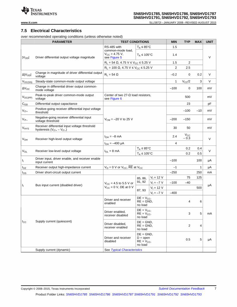
7.5 Electrical Characteristicsover recommended operating conditions (unless otherwise noted)
PARAMETER TEST CONDITIONS MIN TYP MAX UNITRS-485 with TA ≤ 85°C 1.5common-mode load,VCC > 4.75 V, TA ≤ 105°C 1.4
|VOD| Driver differential output voltage magnitude Vsee Figure 5RL = 54 Ω, 4.75 V ≤ VCC ≤ 5.25 V 1.5 2RL = 100 Ω, 4.75 V ≤ VCC ≤ 5.25 V 2 2.5
Change in magnitude of driver differential outputΔ|VOD| RL = 54 Ω –0.2 0 0.2 VvoltageVOC(SS) Steady-state common-mode output voltage 1 VCC/2 3 V
Change in differential driver output common-ΔVOC –100 0 100 mVmode voltagePeak-to-peak driver common-mode output Center of two 27-Ω load resistors,VOC(PP) 500 mVvoltage see Figure 6
COD Differential output capacitance 23 pFPositive-going receiver differential input voltageVIT+ –100 –10 mVthresholdNegative-going receiver differential inputVIT– VCM = –20 V to 25 V –200 –150 mVvoltage thresholdReceiver differential input voltage thresholdVHYS 30 50 mVhysteresis (VIT+ – VIT–)
VCCIOH = –8 mA 2.4 – 0.3VOH Receiver high-level output voltage VIOH = –400 μA 4
TA ≤ 85°C 0.2 0.4VOL Receiver low-level output voltage IOL = 8 mA V
TA ≤ 105°C 0.2 0.5Driver input, driver enable, and receiver enableII –100 100 μAinput current
IOZ Receiver output high-impedance current VO = 0 V or VCC, RE at VCC –1 1 μAIOS Driver short-circuit output current –250 250 mA
VI = 12 V 75 12585, 86,91, 92 VI = –7 V –100 –40VCC = 4.5 to 5.5 V orII Bus input current (disabled driver) μAVCC = 0 V, DE at 0 V VI = 12 V 50087, 93
VI = –7 V –400DE = VCC,Driver and receiver RE = GND, 4 6enabled no loadDE = VCC,Driver enabled, RE = VCC, 3 5 mAreceiver disabled no load
ICC Supply current (quiescent) DE = GND,Driver disabled, RE = GND, 2 4receiver enabled no loadDE = GND,
Driver and receiver D = open 0.5 5 μAdisabled RE = VCC,no load
Supply current (dynamic) See Typical Characteristics
Copyright © 2008–2015, Texas Instruments Incorporated Submit Documentation Feedback 7
Product Folder Links: SN65HVD1785 SN65HVD1786 SN65HVD1787 SN65HVD1791 SN65HVD1792 SN65HVD1793

SN65HVD1785, SN65HVD1786, SN65HVD1787SN65HVD1791, SN65HVD1792, SN65HVD1793SLLS872I –JANUARY 2008–REVISED AUGUST 2015 www.ti.com
7.6 Thermal ConsiderationsPARAMETER TEST CONDITIONS VALUE UNIT
VCC = 5.5 V, TJ = 150°C, RL = 300 Ω, CL = 50 pF (driver),85, 91 290CL = 15 pF (receiver) 5-V supply, unterminated (1)
85, 91VCC = 5.5 V, TJ = 150°C, RL = 100 Ω, CL = 50 pF (driver),86 320CL = 15 pF (receiver) 5-V supply, RS-422 load (1)
PD Power dissipation mW8785, 91
VCC = 5.5 V, TJ = 150°C, RL = 54 Ω, CL = 50 pF (driver),86 400CL = 15 pF (receiver) 5-V supply, RS-485 load (1)
87Thermal-shutdown junctionTSD 170 °Ctemperature
(1) Driver and receiver enabled, 50% duty cycle square-wave signal at signaling rate: HVD1785, 1791 at 115 kbps, HVD1786 at 1 Mbps,HVD1787 at 10 Mbps)
7.7 Switching Characteristicsover recommended operating conditions (unless otherwise noted)
PARAMETER TEST CONDITIONS MIN TYP MAX UNITDRIVER (HVD1785 AND HVD1791)tr, tf Driver differential output rise/fall time 0.4 1.7 2.6 μstPHL, tPLH Driver propagation delay RL = 54 Ω, CL = 50 pF, 0.8 2 μs
see Figure 7Driver differential output pulse skew,tSK(P) 20 250 ns|tPHL – tPLH|tPHZ, tPLZ Driver disable time 0.1 5 μs
See Figure 8 andReceiver enabled 0.2 3Figure 9tPZH, tPZL Driver enable time μsReceiver disabled 3 12
DRIVER (HVD1786 AND HVD1792)tr, tf Driver differential output rise/fall time 50 300 nstPHL, tPLH Driver propagation delay RL = 54 Ω, CL = 50 pF, 200 ns
see Figure 7Driver differential output pulse skew,tSK(P) 25 ns|tPHL – tPLH|tPHZ, tPLZ Driver disable time 3 μs
See Figure 8 andReceiver enabled 300 nsFigure 9tPZH, tPZL Driver enable time Receiver disabled 10 μs
Receiver enabled VCM > VCC 500 nsDRIVER (HVD1787 AND HVD1793)tr, tf Driver differential output rise/fall time 3 30 nstPHL, tPLH Driver propagation delay RL = 54 Ω, CL = 50 pF, 50 ns
see Figure 7Driver differential output pulse skew,tSK(P) 10 ns|tPHL – tPLH|tPHZ, tPLZ Driver disable time 3 μs
See Figure 8 andReceiver enabled 300 nsFigure 9tPZH, tPZL Driver enable time Receiver disabled 9 μs
Receiver enabled VCM > VCC 500 ns
8 Submit Documentation Feedback Copyright © 2008–2015, Texas Instruments Incorporated
Product Folder Links: SN65HVD1785 SN65HVD1786 SN65HVD1787 SN65HVD1791 SN65HVD1792 SN65HVD1793
SN65HVD1785, SN65HVD1786, SN65HVD1787SN65HVD1791, SN65HVD1792, SN65HVD1793
www.ti.com SLLS872I –JANUARY 2008–REVISED AUGUST 2015
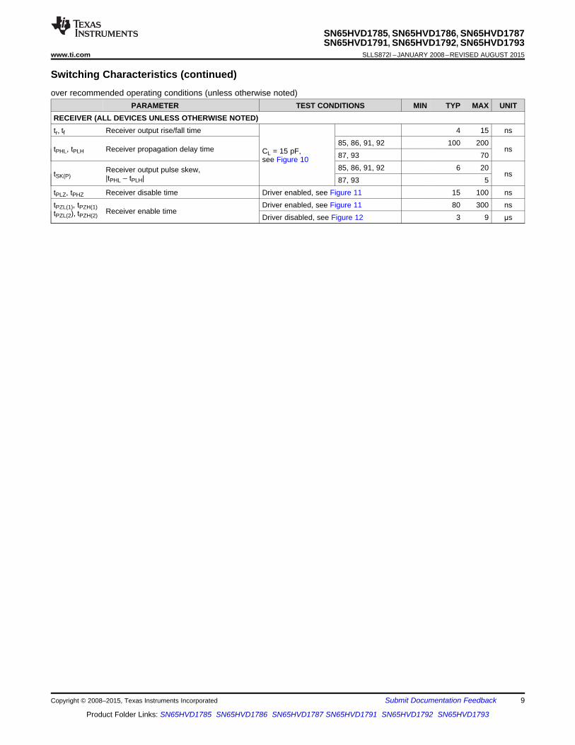
Switching Characteristics (continued)over recommended operating conditions (unless otherwise noted)
PARAMETER TEST CONDITIONS MIN TYP MAX UNITRECEIVER (ALL DEVICES UNLESS OTHERWISE NOTED)tr, tf Receiver output rise/fall time 4 15 ns
85, 86, 91, 92 100 200tPHL, tPLH Receiver propagation delay time nsCL = 15 pF, 87, 93 70see Figure 10
85, 86, 91, 92 6 20Receiver output pulse skew,tSK(P) ns|tPHL – tPLH| 87, 93 5tPLZ, tPHZ Receiver disable time Driver enabled, see Figure 11 15 100 nstPZL(1), tPZH(1) Driver enabled, see Figure 11 80 300 ns
Receiver enable timetPZL(2), tPZH(2) Driver disabled, see Figure 12 3 9 μs
Copyright © 2008–2015, Texas Instruments Incorporated Submit Documentation Feedback 9
Product Folder Links: SN65HVD1785 SN65HVD1786 SN65HVD1787 SN65HVD1791 SN65HVD1792 SN65HVD1793

VIN − Bus Pin Voltage − V
−2.0
−1.5
−1.0
−0.5
0.0
0.5
1.0
1.5
2.0
−90 −60 −30 0 30 60 90
I IN
−B
us P
in C
urr
ent−
mA
G004
00.2
0.4
0.60.8
1
1.2
1.4
1.6
1.8
2
2.2
2.4
2.6
2.8
3
3.2
3.4
3.6
3.84
4.2
4.4
0 2 4 6 8 10 12 14 16 18 20 22 24 26 28 30 32 34 36 38 40 42 44 46 48 50
Idiff - Differential Load Current - mA
V = 5.5 VCC
Load = 300 W Load = 100 W
Load = 60 W
VO
D -
Dif
fere
nti
al O
utp
ut
Vo
ltag
e -
V
V = 5 VCC
V = 4.5 VCC
VCC − Supply Voltage − V
−10
0
10
20
30
40
50
60
70
0.0 0.6 1.2 1.8 2.4 3.0 3.6 4.2 4.8 5.4
I O−
Driver
Outp
ut C
urr
ent−
mA
G001
TA = 25°C
DE at VCC
D at VCC
RL = 54 W
Signaling Rate − Mbps
40
60
80
100
120
0 2 4 6 8 10
I CC
−R
MS
Supply
Curr
ent−
mA
G002
TA = 25°C
RE at VCC
DE at VCC
RL = 54 W
CL = 50 pF
VCC = 5 V
SN65HVD1785, SN65HVD1786, SN65HVD1787SN65HVD1791, SN65HVD1792, SN65HVD1793SLLS872I –JANUARY 2008–REVISED AUGUST 2015 www.ti.com
7.8 Typical Characteristics
Figure 1. Driver Output Current vs Supply Voltage Figure 2. HVD1787 RMS Supply Current vs Signaling Rate
Figure 3. Bus Pin Current vs Bus Pin Voltage Figure 4. Differential Output Voltage vs. Differential LoadCurrent
10 Submit Documentation Feedback Copyright © 2008–2015, Texas Instruments Incorporated
Product Folder Links: SN65HVD1785 SN65HVD1786 SN65HVD1787 SN65HVD1791 SN65HVD1792 SN65HVD1793

0.5 V
3 V
0 V
VOH
» 0 VtPHZ
tPZH
50% 50%VI
VO50%
90%
R = 110L W
± 1%InputGenerator
50 W
3 V
S1
C = 50 pFL ±20%
C Includes FixtureL
and InstrumentationCapacitance
DA
BDE
VO
VI
S0304-01
VOD
RL = 54
1%
W
±50 W
tPLH tPHL
50% 50%
3 V
» 2 V
» –2 V
90%
10%0 V
VI
VOD
tr tf
C = 50 pF 20%L ±
C Includes FixtureL
and InstrumentationCapacitance
DA
B
DE
VCC
VIInput
Generator90%
0 V10%
S0303-01
VOC
27 1%W ±
27 1%W ±
Input
A
B
VA
VB
VOC(PP) DVOC(SS)
VOC
C = 50 pFL ±20%
DA
B
DE
VCC
C Includes Fixture andL
Instrumentation Capacitance
S0302-01
60 1%W ±VOD0 V or 3 V
_+ –20 V < V(test) < 25 V
DE
VCC
A
B
D
375 1%W ±
375 1%W ±
S0301-01
SN65HVD1785, SN65HVD1786, SN65HVD1787SN65HVD1791, SN65HVD1792, SN65HVD1793
www.ti.com SLLS872I –JANUARY 2008–REVISED AUGUST 2015
8 Parameter Measurement Information
Input generator rate is 100 kbps, 50% duty cycle, rise and fall times less than 6 nsec, output impedance 50 Ω.
Figure 5. Measurement of Driver Differential Output Voltage With Common-Mode Load
Figure 6. Measurement of Driver Differential and Common-Mode Output With RS-485 Load
Figure 7. Measurement of Driver Differential Output Rise and Fall Times and Propagation Delays
NOTE: D at 3 V to test non-inverting output, D at 0 V to test inverting output.
Figure 8. Measurement of Driver Enable and Disable Times With Active High Output and Pulldown Load
Copyright © 2008–2015, Texas Instruments Incorporated Submit Documentation Feedback 11
Product Folder Links: SN65HVD1785 SN65HVD1786 SN65HVD1787 SN65HVD1791 SN65HVD1792 SN65HVD1793

InputGenerator
50 W
VO
1.5 V
0 V
50% 50%
3 V
VOH
VOL
50%10%
50%
tPLH tPHL
tftr
90%
VI
VO
C = 15 pF 20%L ±
C Includes Fixture
and InstrumentationCapacitance
L
A
B
RE
VI
R
0 V
90%
10%
S0306-01
InputGenerator 50 W
3 V VO
S1
3 V
50%
50%
50%
tPZL tPLZ
10%
» 3 V
0 V
VOL
VI
VO
R = 110L W
±1%
CL = 50 pF ±20%
C Includes FixtureL
and InstrumentationCapacitance
DA
BDE
VI
» 3 V
S0305-01
SN65HVD1785, SN65HVD1786, SN65HVD1787SN65HVD1791, SN65HVD1792, SN65HVD1793SLLS872I –JANUARY 2008–REVISED AUGUST 2015 www.ti.com
Parameter Measurement Information (continued)
NOTE: D at 0 V to test non-inverting output, D at 3 V to test inverting output.
Figure 9. Measurement of Driver Enable and Disable Times With Active-Low Output and Pullup Load
Figure 10. Measurement of Receiver Output Rise and Fall Times and Propagation Delays
12 Submit Documentation Feedback Copyright © 2008–2015, Texas Instruments Incorporated
Product Folder Links: SN65HVD1785 SN65HVD1786 SN65HVD1787 SN65HVD1791 SN65HVD1792 SN65HVD1793

50 W
VO
RE
RA
B
3 V
0 V or 3 V
VCC
50% 50%
tPZH(1) tPHZ
50%90%
3 V
0 V
VOH
» 0 V
VO
C = 15 pF 20%L ±
C Includes Fixture
and InstrumentationCapacitance
L
VI
DE
D1 k 1%W ±
VI
S1
D at 3 VS1 to GND
tPZL(1) tPLZ
50%10%
VCC
VOL
VO
D at 0 VS1 to VCC
InputGenerator
S0307-01
SN65HVD1785, SN65HVD1786, SN65HVD1787SN65HVD1791, SN65HVD1792, SN65HVD1793
www.ti.com SLLS872I –JANUARY 2008–REVISED AUGUST 2015
Parameter Measurement Information (continued)
Figure 11. Measurement of Receiver Enable/Disable Times With Driver Enabled
Copyright © 2008–2015, Texas Instruments Incorporated Submit Documentation Feedback 13
Product Folder Links: SN65HVD1785 SN65HVD1786 SN65HVD1787 SN65HVD1791 SN65HVD1792 SN65HVD1793

InputGenerator 50 W
VO
RE
RA
B
VCC
50%
50%
50%
tPZH(2)
3 V
0 V
VOH
GND
VI
VO
VO
0 V or 1.5 V
1.5 V or 0 V C = 15 pF 20%±L
C Includes FixtureL
and InstrumentationCapacitanceVI
1 kW ± 1%
A at 1.5 VB at 0 VS1 to GND
tPZL(2)
VCC
VOL
A at 0 VB at 1.5 VS1 to VCC
S1
S0308-01
SN65HVD1785, SN65HVD1786, SN65HVD1787SN65HVD1791, SN65HVD1792, SN65HVD1793SLLS872I –JANUARY 2008–REVISED AUGUST 2015 www.ti.com
Parameter Measurement Information (continued)
Figure 12. Measurement of Receiver Enable Times With Driver Disabled
14 Submit Documentation Feedback Copyright © 2008–2015, Texas Instruments Incorporated
Product Folder Links: SN65HVD1785 SN65HVD1786 SN65HVD1787 SN65HVD1791 SN65HVD1792 SN65HVD1793

Logic Diagram (Positive Logic)
2
3
4
5
12
10
9
11
A
Z
Y
B
R
RE
DE
D
S0300-01
1
2
3
4
6
7
A
B
R
RE
DE
D
Bus
SN65HVD1785, SN65HVD1786, SN65HVD1787SN65HVD1791, SN65HVD1792, SN65HVD1793
www.ti.com SLLS872I –JANUARY 2008–REVISED AUGUST 2015
9 Detailed Description
9.1 OverviewThe SN65HVD17xx family of RS-485 transceivers are designed to operate up to 115 kbps (HVD1785 andHVD1791), 1 Mbps (HVD1786 and HVD1792), or 10 Mbps (HVD1787 or HVD1793) and to withstand DCovervoltage faults on the bus interface pins. This helps to protect the devices against damages resulting fromdirect shorts to power supplies, cable mis-wirings, connector failures, or other common faults.
The SN65HVD178x devices are half-duplex, and thus have the transmitter and receiver bus interfaces connectedtogether internally. The SN65HVD179x family leaves these two interfaces separate, allowing for full-duplexcommunication. The low receiver loading allows for up to 256 nodes to share a common RS-485 bus. Thedevices feature a wide common-mode range as well as fail-safe receivers, which ensure a stable logic-leveloutput during bus open, short, or idle conditions.
9.2 Functional Block Diagram
Figure 13. Half-Duplex Transceiver
Figure 14. Full Duplex Transceiver
9.3 Feature Description
9.3.1 Hot-PluggingThese devices are designed to operate in hot swap or hot pluggable applications. Key features for hot-pluggableapplications are power-up, power-down glitch free operation, default disabled input/output pins, and receiverfailsafe. As shown in Figure 1, an internal Power-On Reset circuit keeps the driver outputs in a high-impedancestate until the supply voltage has reached a level at which the device will reliably operate. This ensures that nospurious transitions (glitches) will occur on the bus pin outputs as the power supply turns on or turns off.
As shown in Device Functional Modes, the ENABLE inputs have the feature of default disable on both the driverenable and receiver enable. This ensures that the device will neither drive the bus nor report data on the R pinuntil the associated controller actively drives the enable pins.
Copyright © 2008–2015, Texas Instruments Incorporated Submit Documentation Feedback 15
Product Folder Links: SN65HVD1785 SN65HVD1786 SN65HVD1787 SN65HVD1791 SN65HVD1792 SN65HVD1793

SN65HVD1785, SN65HVD1786, SN65HVD1787SN65HVD1791, SN65HVD1792, SN65HVD1793SLLS872I –JANUARY 2008–REVISED AUGUST 2015 www.ti.com
Feature Description (continued)9.3.2 Receiver FailsafeThe differential receiver is failsafe to invalid bus states caused by:
• open bus conditions such as a disconnected connector,• shorted bus conditions such as cable damage shorting the twisted-pair together,• or idle bus conditions that occur when no driver on the bus is actively driving.
In any of these cases, the differential receiver outputs a failsafe logic High state, so that the output of thereceiver is not indeterminate.
In the HVD17xx family of RS-485 devices, receiver failsafe is accomplished by offsetting the receiver thresholdsso that the “input indeterminate” range does not include zero volts differential. In order to comply with the RS-422and RS-485 standards, the receiver output must output a High when the differential input VID is more positivethan 200 mV, and must output a Low when the VID is more negative than -200 mV. The HVD17xx receiverparameters which determine the failsafe performance are VIT+ and VIT– and VHYS. In the Electrical Characteristicstable, VIT– has a typical value of –150 mV and a minimum (most negative) value of -200 mV, so differentialsignals more negative than -200 mV will always cause a Low receiver output. Similarly, differential signals morepositive than 200 mV will always cause a High receiver output, because the typical value of VIT+ is -100mV, andVIT+ is never more positive than -10 mV under any conditions of temperature, supply voltage, or common-modeoffset.
When the differential input signal is close to zero, it will still be above the VIT+ threshold, and the receiver outputwill be High. Only when the differential input is more negative than VIT- will the receiver output transition to a Lowstate. So, the noise immunity of the receiver inputs during a bus fault condition includes the receiver hysteresisvalue VHYS (the separation between VIT+ and VIT– ) as well as the value of VIT+.
For the HVD17xx devices, the typical noise immunity is typically about 150 mV, which is the negative noise levelneeded to exceed the VIT– threshold (VIT- TYP = –150 mV). In the worst case, the failsafe noise immunity is neverless than 40 mV, which is set by the maximum positive threshold (VIT+ MAX = –10 mV) plus the minimumhysteresis voltage (VHYS MIN = 30 mV).
9.3.3 70-V Fault-ProtectionThe SN65HVD17xx family of RS-485 devices is designed to survive bus pin faults up to ±70V. The devicesdesigned for fast signaling rate (10 Mbps) will not survive a bus pin fault with a direct short to voltages above30V when:
1. the device is powered on AND2a. the driver is enabled (DE=HIGH) AND D=HIGH AND the bus fault is applied to the A pin OR2b. the driver is enabled (DE=HIGH) AND D=LOW AND the bus fault is applied to the B pin
Under other conditions, the device will survive shorts to bus pin faults up to 70V. Table 1 summarizes theconditions under which the device may be damaged, and the conditions under which the device will not bedamaged.
16 Submit Documentation Feedback Copyright © 2008–2015, Texas Instruments Incorporated
Product Folder Links: SN65HVD1785 SN65HVD1786 SN65HVD1787 SN65HVD1791 SN65HVD1792 SN65HVD1793

2
3
8
6
5
7
A
Z
Y
B
R
D
S0310-01
S0309-01
1
2
3
4
6
7
A
B
R
RE
DE
D
SN65HVD1785, SN65HVD1786, SN65HVD1787SN65HVD1791, SN65HVD1792, SN65HVD1793
www.ti.com SLLS872I –JANUARY 2008–REVISED AUGUST 2015
Feature Description (continued)Table 1. Device Conditions
POWER DE D A B RESULTSOFF X X -70V < VA < 70V -70V < VB < 70V Device survivesON LO X -70V < VA < 70V -70V < VB < 70V Device survivesON HI L -70V < VA < 70V -70V < VB < 30V Device survivesON HI L -70V < VA < 70V 30V < VB Damage may occurON HI H -70V < VA < 30V -70V < VB < 30V Device survivesON HI H 30V < VA -70V < VB < 30V Damage may occur
9.3.4 Additional OptionsThe SN65HVD17xx family also has options for J1708 applications, for always-enabled full-duplex versions(industry-standard SN65LBC179 footprint) and for inverting-polarity versions, which allow users to correct areversal of the bus wires without re-wiring. Contact your local Texas Instruments representative for informationon these options.
Table 2. SN65HVD17xx Options for J1708 ApplicationsPART NUMBER SN65HVD17xxFOOTPRINT/FUNCTION SLOW MEDIUM FASTHalf-duplex (176 pinout) 85 86 87Full-duplex no enables (179 pinout) 88 89 90Full-duplex with enables (180 pinout) 91 92 93Half-duplex with cable invert 94 95 96Full-duplex with cable invert and enables 97 98 99J1708 08 09 10
Figure 15. SN65HVD1708E Transceiver for J1708 Applications
Figure 16. SN65HVD17xx Always-Enabled Driver Receiver
Copyright © 2008–2015, Texas Instruments Incorporated Submit Documentation Feedback 17
Product Folder Links: SN65HVD1785 SN65HVD1786 SN65HVD1787 SN65HVD1791 SN65HVD1792 SN65HVD1793

3
4
1
2
6
7
A
B
R
DE
D
INV
S0311-01
4
5
8
2
3
1
9
10
11
12
Y
Z
B
AR
DE
D
DINV
RE
RINV
SN65HVD1785, SN65HVD1786, SN65HVD1787SN65HVD1791, SN65HVD1792, SN65HVD1793SLLS872I –JANUARY 2008–REVISED AUGUST 2015 www.ti.com
Figure 17. SN65HVD17xx Options With Inverting Feature to Correct for Miswired Cables
9.4 Device Functional Modes
Table 3. Driver Function Table
INPUT ENABLE OUTPUTS
D DE A B
H H H L Actively drive bus high
L H L H Actively drive bus low
X L Z Z Driver disabled
X OPEN Z Z Driver disabled by default
OPEN H H L Actively drive bus high by default
Table 4. Receiver Function Table
DIFFERENTIAL INPUT ENABLE OUTPUT
VID = VA – VB RE R
VIT+ < VID L H Receive valid bus high
VIT– < VID < VIT+ L ? Indeterminate bus state
VID < VIT– L L Receive valid bus low
X H Z Receiver disabled
X OPEN Z Receiver disabled by default
Open-circuit bus L H Fail-safe high output
Short-circuit bus L H Fail-safe high output
Idle (terminated) bus L H Fail-safe high output
18 Submit Documentation Feedback Copyright © 2008–2015, Texas Instruments Incorporated
Product Folder Links: SN65HVD1785 SN65HVD1786 SN65HVD1787 SN65HVD1791 SN65HVD1792 SN65HVD1793
RT RT
R
DR
DE
RE
D
Y
Z R
D
R
RE
DE
D
A
B
RT RT
B
A
Z
Y
R
D
R RE DE D
Z YBA
Master Slave
Slave
RT RT
R
A B
R RE DE D
DR
A B
R RE DE D
D
R
D
R
RE
DE
D
A
B
R
D
R
RE
DE
D
A
B
SN65HVD1785, SN65HVD1786, SN65HVD1787SN65HVD1791, SN65HVD1792, SN65HVD1793
www.ti.com SLLS872I –JANUARY 2008–REVISED AUGUST 2015
10 Application and Implementation
NOTEInformation in the following applications sections is not part of the TI componentspecification, and TI does not warrant its accuracy or completeness. TI’s customers areresponsible for determining suitability of components for their purposes. Customers shouldvalidate and test their design implementation to confirm system functionality.
10.1 Application InformationThe SN65HVD17xx family consists of both half-duplex and full-duplex transceivers that can be used forasynchronous data communication. Half-duplex implementations require one signaling pair (two wires), while full-duplex implementations require two signaling pairs (four wires). The driver and receiver enable pins of theSN65HVD17xx family allow for control over the direction of data flow. Since it is common for multiple transceiversto share a common communications bus, care should be taken at the system level to ensure that only one driveris enabled at a time. This avoids bus contention, a fault condition in which multiple drivers attempt to send dataat the same time.
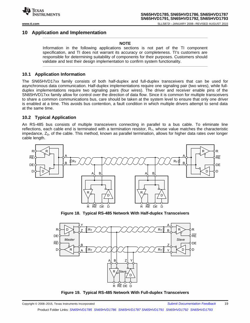
10.2 Typical ApplicationAn RS-485 bus consists of multiple transceivers connecting in parallel to a bus cable. To eliminate linereflections, each cable end is terminated with a termination resistor, RT, whose value matches the characteristicimpedance, Z0, of the cable. This method, known as parallel termination, allows for higher data rates over longercable length.
Figure 18. Typical RS-485 Network With Half-duplex Transceivers
Figure 19. Typical RS-485 Network With Full-duplex Transceivers
Copyright © 2008–2015, Texas Instruments Incorporated Submit Documentation Feedback 19
Product Folder Links: SN65HVD1785 SN65HVD1786 SN65HVD1787 SN65HVD1791 SN65HVD1792 SN65HVD1793

stub rL 0.1 t v c£ ´ ´ ´
10000
1000
100
10
Cab
le L
en
gth
(ft
)
100 1k 10k 100k 1M 10M 100M
Data Rate (bps)
Conservative
Characteristics
5%, 10%, and 20% Jitter
SN65HVD1785, SN65HVD1786, SN65HVD1787SN65HVD1791, SN65HVD1792, SN65HVD1793SLLS872I –JANUARY 2008–REVISED AUGUST 2015 www.ti.com
Typical Application (continued)10.2.1 Design RequirementsRS-485 is a robust electrical standard suitable for long-distance networking that may be used in a wide range ofapplications with varying requirements, such as distance, data rate, and number of nodes.
10.2.1.1 Data Rate and Bus LengthThere is an inverse relationship between data rate and cable length, which means the higher the data rate, theshort the cable length; and conversely, the lower the data rate, the longer the cable length. While most RS-485systems use data rates between 10 kbps and 100 kbps, some applications require data rates up to 250 kbps atdistances of 4000 feet and longer. Longer distances are possible by allowing for small signal jitter of up to 5 or10%.
Figure 20. Cable Length vs Data Rate Characteristic
Even higher data rates are achievable (for example, 10 Mbps for the SN65HVD1787 and SN65HVD1793) incases where the interconnect is short enough (or has suitably low attenuation at signal frequencies) to notdegrade the data.
10.2.1.2 Stub LengthWhen connecting a node to the bus, the distance between the transceiver inputs and the cable trunk, known asthe stub, should be as short as possible. Stubs present a non-terminated piece of bus line which can introducereflections as the length of the stub increases. As a general guideline, the electrical length, or round-trip delay, ofa stub should be less than one-tenth of the rise time of the driver, thus giving a maximum physical stub length asshown in Equation 1.
where• tr is the 10/90 rise time of the driver• c is the speed of light (3 × 10⁸ m/s)• v is the signal velocity of the cable or trace as a factor of c (1)
10.2.1.3 Receiver FailsafeThe differential receiver of the SN75HVD17xx family is failsafe to invalid bus states caused by:• Open bus conditions, such as a disconnected connector• Shorted bus conditions, such as cable damage shorting the twisted-pair together• Idle bus conditions that occur when no driver on the bus is actively drivingn any of these cases, the differential receiver will output a failsafe logic high state so that the output of thereceiver is not indeterminate.
20 Submit Documentation Feedback Copyright © 2008–2015, Texas Instruments Incorporated
Product Folder Links: SN65HVD1785 SN65HVD1786 SN65HVD1787 SN65HVD1791 SN65HVD1792 SN65HVD1793
SN65HVD1785, SN65HVD1786, SN65HVD1787SN65HVD1791, SN65HVD1792, SN65HVD1793
www.ti.com SLLS872I –JANUARY 2008–REVISED AUGUST 2015
Typical Application (continued)Receiver failsafe is accomplished by offsetting the receiver thresholds such that the “input indeterminate” rangedoes not include zero volts differential. In order to comply with the RS-422 and RS-485 standards, the receiveroutput must output a high when the differential input VID is more positive than +200 mV, and must output a lowwhen VID is more negative than -200 mV. The receiver parameters which determine the failsafe performance areVIT(+) and VIT(-). As shown in the Electrical Characteristics table, differential signals more negative than -200 mVwill always cause a low receiver output, and differential signals more positive than +200 mV will always cause ahigh receiver output.
When the differential input signal is close to zero, it is still above the maximum VIT(+) threshold of -10 mV, and thereceiver output will be high.
10.2.2 Detailed Design ProcedureAlthough the SN65HVD17xx family is internally protected against human-body-model ESD strikes up to 16 kV,additional protection against higher-energy transients can be provided at the application level by implementingexternal protection devices.
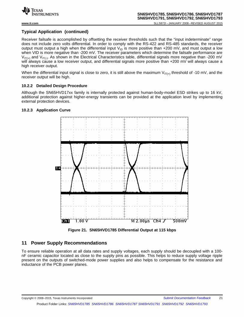
10.2.3 Application Curve
Figure 21. SN65HVD1785 Differential Output at 115 kbps
11 Power Supply RecommendationsTo ensure reliable operation at all data rates and supply voltages, each supply should be decoupled with a 100-nF ceramic capacitor located as close to the supply pins as possible. This helps to reduce supply voltage ripplepresent on the outputs of switched-mode power supplies and also helps to compensate for the resistance andinductance of the PCB power planes.
Copyright © 2008–2015, Texas Instruments Incorporated Submit Documentation Feedback 21
Product Folder Links: SN65HVD1785 SN65HVD1786 SN65HVD1787 SN65HVD1791 SN65HVD1792 SN65HVD1793

MCU
R
R
Via to ground
SN65HVD1785
JM
P
R
R
R
C
5
6
6
1
4R
5
Via to VCC
TVS
75
SN65HVD1785, SN65HVD1786, SN65HVD1787SN65HVD1791, SN65HVD1792, SN65HVD1793SLLS872I –JANUARY 2008–REVISED AUGUST 2015 www.ti.com
12 Layout
12.1 Layout GuidelinesTo ensure reliable operation at all data rates and supply voltages, each supply should be decoupled with a 100-nF ceramic capacitor located as close to the supply pins as possible. This helps to reduce supply voltage ripplepresent on the outputs of switched-mode power supplies and also helps to compensate for the resistance andinductance of the PCB power planes.1. Place the protection circuitry close to the bus connector to prevent noise transients from entering the board.2. Use VCC and ground planes to provide low-inductance power distribution. Note that high-frequency currents
tend to follow the path of least inductance and not the path of least resistance.3. Design the protection components into the direction of the signal path. Do not force the transient currents to
divert from the signal path to reach the protection device.4. Apply 100-nF-to-220-nF bypass capacitors as close as possible to the VCC pins of transceiver, UART, or
controller ICs on the board.5. Use at least two vias for VCC and ground connections of bypass capacitors and protection devices to
minimize effective via-inductance.6. Use 1-kΩ-to-10-kΩ pullup and pulldown resistors for enable lines to limit noise currents in these lines during
transient events.7. Insert series pulse-proof resistors into the A and B bus lines if the TVS clamping voltage is higher than the
specified maximum voltage of the transceiver bus terminals. These resistors limit the residual clampingcurrent into the transceiver and prevent it from latching up.
8. While pure TVS protection is sufficient for surge transients up to 1 kV, higher transients require metal-oxidevaristors (MOVs) which reduce the transients to a few hundred volts of clamping voltage, and transientblocking units (TBUs) that limit transient current to less than 1 mA.
12.2 Layout Example
Figure 22. Layout Example (Half-Duplex Transceiver)
22 Submit Documentation Feedback Copyright © 2008–2015, Texas Instruments Incorporated
Product Folder Links: SN65HVD1785 SN65HVD1786 SN65HVD1787 SN65HVD1791 SN65HVD1792 SN65HVD1793

MCU
R
R
Via to ground
JM
P
R
R
R
C
5
6
6
1
4R
5
Via to VCC
TVS7 5
R
R JM
PR
1
TVS
7
5
SN65HVD1791
SN65HVD1785, SN65HVD1786, SN65HVD1787SN65HVD1791, SN65HVD1792, SN65HVD1793
www.ti.com SLLS872I –JANUARY 2008–REVISED AUGUST 2015
Layout Example (continued)
Figure 23. Layout Example (Full-Duplex Transceiver)
13 Device and Documentation Support
13.1 Documentation SupportFor related documentation see the following:
SN65HVD1781, Fault-Protected RS-485 Transceivers With 3.3-V to 5-V Operation, (SLLS877)
13.2 Related LinksThe table below lists quick access links. Categories include technical documents, support and communityresources, tools and software, and quick access to sample or buy.
Table 5. Related LinksTECHNICAL TOOLS & SUPPORT &PARTS PRODUCT FOLDER SAMPLE & BUY DOCUMENTS SOFTWARE COMMUNITY
SN65HVD1785 Click here Click here Click here Click here Click hereSN65HVD1786 Click here Click here Click here Click here Click hereSN65HVD1787 Click here Click here Click here Click here Click hereSN65HVD1791 Click here Click here Click here Click here Click hereSN65HVD1792 Click here Click here Click here Click here Click hereSN65HVD1793 Click here Click here Click here Click here Click here
Copyright © 2008–2015, Texas Instruments Incorporated Submit Documentation Feedback 23
Product Folder Links: SN65HVD1785 SN65HVD1786 SN65HVD1787 SN65HVD1791 SN65HVD1792 SN65HVD1793

SN65HVD1785, SN65HVD1786, SN65HVD1787SN65HVD1791, SN65HVD1792, SN65HVD1793SLLS872I –JANUARY 2008–REVISED AUGUST 2015 www.ti.com
13.3 Community ResourcesThe following links connect to TI community resources. Linked contents are provided "AS IS" by the respectivecontributors. They do not constitute TI specifications and do not necessarily reflect TI's views; see TI's Terms ofUse.
TI E2E™ Online Community TI's Engineer-to-Engineer (E2E) Community. Created to foster collaborationamong engineers. At e2e.ti.com, you can ask questions, share knowledge, explore ideas and helpsolve problems with fellow engineers.
Design Support TI's Design Support Quickly find helpful E2E forums along with design support tools andcontact information for technical support.
13.4 TrademarksE2E is a trademark of Texas Instruments.All other trademarks are the property of their respective owners.
13.5 Electrostatic Discharge CautionThese devices have limited built-in ESD protection. The leads should be shorted together or the device placed in conductive foamduring storage or handling to prevent electrostatic damage to the MOS gates.
13.6 GlossarySLYZ022 — TI Glossary.
This glossary lists and explains terms, acronyms, and definitions.
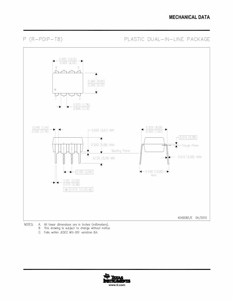
14 Mechanical, Packaging, and Orderable InformationThe following pages include mechanical, packaging, and orderable information. This information is the mostcurrent data available for the designated devices. This data is subject to change without notice and revision ofthis document. For browser-based versions of this data sheet, refer to the left-hand navigation.
24 Submit Documentation Feedback Copyright © 2008–2015, Texas Instruments Incorporated
Product Folder Links: SN65HVD1785 SN65HVD1786 SN65HVD1787 SN65HVD1791 SN65HVD1792 SN65HVD1793

PACKAGE OPTION ADDENDUM
www.ti.com 24-Apr-2015
Addendum-Page 1
PACKAGING INFORMATION
Orderable Device Status(1)
Package Type PackageDrawing
Pins PackageQty
Eco Plan(2)
Lead/Ball Finish(6)
MSL Peak Temp(3)
Op Temp (°C) Device Marking(4/5)
Samples
SN65HVD1785D ACTIVE SOIC D 8 75 Green (RoHS& no Sb/Br)
CU NIPDAU Level-1-260C-UNLIM -40 to 105 VP1785
SN65HVD1785DG4 ACTIVE SOIC D 8 75 Green (RoHS& no Sb/Br)
CU NIPDAU Level-1-260C-UNLIM -40 to 105 VP1785
SN65HVD1785DR ACTIVE SOIC D 8 2500 Green (RoHS& no Sb/Br)
CU NIPDAU Level-1-260C-UNLIM -40 to 105 VP1785
SN65HVD1785DRG4 ACTIVE SOIC D 8 2500 Green (RoHS& no Sb/Br)
CU NIPDAU Level-1-260C-UNLIM -40 to 105 VP1785
SN65HVD1785P ACTIVE PDIP P 8 50 Green (RoHS& no Sb/Br)
CU NIPDAU N / A for Pkg Type -40 to 105 65HVD1785
SN65HVD1786D ACTIVE SOIC D 8 75 Green (RoHS& no Sb/Br)
CU NIPDAU Level-1-260C-UNLIM -40 to 105 VP1786
SN65HVD1786DG4 ACTIVE SOIC D 8 75 Green (RoHS& no Sb/Br)
CU NIPDAU Level-1-260C-UNLIM -40 to 105 VP1786
SN65HVD1786DR ACTIVE SOIC D 8 2500 Green (RoHS& no Sb/Br)
CU NIPDAU Level-1-260C-UNLIM -40 to 105 VP1786
SN65HVD1786DRG4 ACTIVE SOIC D 8 2500 Green (RoHS& no Sb/Br)
CU NIPDAU Level-1-260C-UNLIM -40 to 105 VP1786
SN65HVD1786P ACTIVE PDIP P 8 50 Green (RoHS& no Sb/Br)
CU NIPDAU N / A for Pkg Type -40 to 105 65HVD1786
SN65HVD1787D ACTIVE SOIC D 8 75 Green (RoHS& no Sb/Br)
CU NIPDAU Level-1-260C-UNLIM -40 to 105 VP1787
SN65HVD1787DR ACTIVE SOIC D 8 2500 Green (RoHS& no Sb/Br)
CU NIPDAU Level-1-260C-UNLIM -40 to 105 VP1787
SN65HVD1787P ACTIVE PDIP P 8 50 Green (RoHS& no Sb/Br)
CU NIPDAU N / A for Pkg Type -40 to 105 65HVD1787
SN65HVD1791D ACTIVE SOIC D 14 50 Green (RoHS& no Sb/Br)
CU NIPDAU Level-1-260C-UNLIM -40 to 105 VP1791
SN65HVD1791DG4 ACTIVE SOIC D 14 50 Green (RoHS& no Sb/Br)
CU NIPDAU Level-1-260C-UNLIM -40 to 105 VP1791
SN65HVD1791DR ACTIVE SOIC D 14 2500 Green (RoHS& no Sb/Br)
CU NIPDAU Level-1-260C-UNLIM -40 to 105 VP1791
SN65HVD1791DRG4 ACTIVE SOIC D 14 2500 Green (RoHS& no Sb/Br)
CU NIPDAU Level-1-260C-UNLIM -40 to 105 VP1791

PACKAGE OPTION ADDENDUM
www.ti.com 24-Apr-2015
Addendum-Page 2
Orderable Device Status(1)
Package Type PackageDrawing
Pins PackageQty
Eco Plan(2)
Lead/Ball Finish(6)
MSL Peak Temp(3)
Op Temp (°C) Device Marking(4/5)
Samples
SN65HVD1792D ACTIVE SOIC D 14 50 Green (RoHS& no Sb/Br)
CU NIPDAU Level-1-260C-UNLIM -40 to 105 VP1792
SN65HVD1792DR ACTIVE SOIC D 14 2500 Green (RoHS& no Sb/Br)
CU NIPDAU Level-1-260C-UNLIM -40 to 105 VP1792
SN65HVD1793D ACTIVE SOIC D 14 50 Green (RoHS& no Sb/Br)
CU NIPDAU Level-1-260C-UNLIM -40 to 105 VP1793
SN65HVD1793DR ACTIVE SOIC D 14 2500 Green (RoHS& no Sb/Br)
CU NIPDAU Level-1-260C-UNLIM -40 to 105 VP1793
(1) The marketing status values are defined as follows:ACTIVE: Product device recommended for new designs.LIFEBUY: TI has announced that the device will be discontinued, and a lifetime-buy period is in effect.NRND: Not recommended for new designs. Device is in production to support existing customers, but TI does not recommend using this part in a new design.PREVIEW: Device has been announced but is not in production. Samples may or may not be available.OBSOLETE: TI has discontinued the production of the device.
(2) Eco Plan - The planned eco-friendly classification: Pb-Free (RoHS), Pb-Free (RoHS Exempt), or Green (RoHS & no Sb/Br) - please check http://www.ti.com/productcontent for the latest availabilityinformation and additional product content details.TBD: The Pb-Free/Green conversion plan has not been defined.Pb-Free (RoHS): TI's terms "Lead-Free" or "Pb-Free" mean semiconductor products that are compatible with the current RoHS requirements for all 6 substances, including the requirement thatlead not exceed 0.1% by weight in homogeneous materials. Where designed to be soldered at high temperatures, TI Pb-Free products are suitable for use in specified lead-free processes.Pb-Free (RoHS Exempt): This component has a RoHS exemption for either 1) lead-based flip-chip solder bumps used between the die and package, or 2) lead-based die adhesive used betweenthe die and leadframe. The component is otherwise considered Pb-Free (RoHS compatible) as defined above.Green (RoHS & no Sb/Br): TI defines "Green" to mean Pb-Free (RoHS compatible), and free of Bromine (Br) and Antimony (Sb) based flame retardants (Br or Sb do not exceed 0.1% by weightin homogeneous material)
(3) MSL, Peak Temp. - The Moisture Sensitivity Level rating according to the JEDEC industry standard classifications, and peak solder temperature.
(4) There may be additional marking, which relates to the logo, the lot trace code information, or the environmental category on the device.
(5) Multiple Device Markings will be inside parentheses. Only one Device Marking contained in parentheses and separated by a "~" will appear on a device. If a line is indented then it is a continuationof the previous line and the two combined represent the entire Device Marking for that device.
(6) Lead/Ball Finish - Orderable Devices may have multiple material finish options. Finish options are separated by a vertical ruled line. Lead/Ball Finish values may wrap to two lines if the finishvalue exceeds the maximum column width.
Important Information and Disclaimer:The information provided on this page represents TI's knowledge and belief as of the date that it is provided. TI bases its knowledge and belief on informationprovided by third parties, and makes no representation or warranty as to the accuracy of such information. Efforts are underway to better integrate information from third parties. TI has taken and

PACKAGE OPTION ADDENDUM
www.ti.com 24-Apr-2015
Addendum-Page 3
continues to take reasonable steps to provide representative and accurate information but may not have conducted destructive testing or chemical analysis on incoming materials and chemicals.TI and TI suppliers consider certain information to be proprietary, and thus CAS numbers and other limited information may not be available for release.
In no event shall TI's liability arising out of such information exceed the total purchase price of the TI part(s) at issue in this document sold by TI to Customer on an annual basis.
OTHER QUALIFIED VERSIONS OF SN65HVD1792 :
• Enhanced Product: SN65HVD1792-EP
NOTE: Qualified Version Definitions:
• Enhanced Product - Supports Defense, Aerospace and Medical Applications

TAPE AND REEL INFORMATION
*All dimensions are nominal
Device PackageType
PackageDrawing
Pins SPQ ReelDiameter
(mm)
ReelWidth
W1 (mm)
A0(mm)
B0(mm)
K0(mm)
P1(mm)
W(mm)
Pin1Quadrant
SN65HVD1785DR SOIC D 8 2500 330.0 12.4 6.4 5.2 2.1 8.0 12.0 Q1
SN65HVD1786DR SOIC D 8 2500 330.0 12.4 6.4 5.2 2.1 8.0 12.0 Q1
SN65HVD1787DR SOIC D 8 2500 330.0 12.4 6.4 5.2 2.1 8.0 12.0 Q1
SN65HVD1791DR SOIC D 14 2500 330.0 16.4 6.5 9.0 2.1 8.0 16.0 Q1
SN65HVD1792DR SOIC D 14 2500 330.0 16.4 6.5 9.0 2.1 8.0 16.0 Q1
SN65HVD1793DR SOIC D 14 2500 330.0 16.4 6.5 9.0 2.1 8.0 16.0 Q1
PACKAGE MATERIALS INFORMATION
www.ti.com 20-Mar-2015
Pack Materials-Page 1

*All dimensions are nominal
Device Package Type Package Drawing Pins SPQ Length (mm) Width (mm) Height (mm)
SN65HVD1785DR SOIC D 8 2500 367.0 367.0 35.0
SN65HVD1786DR SOIC D 8 2500 367.0 367.0 35.0
SN65HVD1787DR SOIC D 8 2500 367.0 367.0 35.0
SN65HVD1791DR SOIC D 14 2500 367.0 367.0 38.0
SN65HVD1792DR SOIC D 14 2500 367.0 367.0 38.0
SN65HVD1793DR SOIC D 14 2500 367.0 367.0 38.0
PACKAGE MATERIALS INFORMATION
www.ti.com 20-Mar-2015
Pack Materials-Page 2


IMPORTANT NOTICE
Texas Instruments Incorporated and its subsidiaries (TI) reserve the right to make corrections, enhancements, improvements and otherchanges to its semiconductor products and services per JESD46, latest issue, and to discontinue any product or service per JESD48, latestissue. Buyers should obtain the latest relevant information before placing orders and should verify that such information is current andcomplete. All semiconductor products (also referred to herein as “components”) are sold subject to TI’s terms and conditions of salesupplied at the time of order acknowledgment.TI warrants performance of its components to the specifications applicable at the time of sale, in accordance with the warranty in TI’s termsand conditions of sale of semiconductor products. Testing and other quality control techniques are used to the extent TI deems necessaryto support this warranty. Except where mandated by applicable law, testing of all parameters of each component is not necessarilyperformed.TI assumes no liability for applications assistance or the design of Buyers’ products. Buyers are responsible for their products andapplications using TI components. To minimize the risks associated with Buyers’ products and applications, Buyers should provideadequate design and operating safeguards.TI does not warrant or represent that any license, either express or implied, is granted under any patent right, copyright, mask work right, orother intellectual property right relating to any combination, machine, or process in which TI components or services are used. Informationpublished by TI regarding third-party products or services does not constitute a license to use such products or services or a warranty orendorsement thereof. Use of such information may require a license from a third party under the patents or other intellectual property of thethird party, or a license from TI under the patents or other intellectual property of TI.Reproduction of significant portions of TI information in TI data books or data sheets is permissible only if reproduction is without alterationand is accompanied by all associated warranties, conditions, limitations, and notices. TI is not responsible or liable for such altereddocumentation. Information of third parties may be subject to additional restrictions.Resale of TI components or services with statements different from or beyond the parameters stated by TI for that component or servicevoids all express and any implied warranties for the associated TI component or service and is an unfair and deceptive business practice.TI is not responsible or liable for any such statements.Buyer acknowledges and agrees that it is solely responsible for compliance with all legal, regulatory and safety-related requirementsconcerning its products, and any use of TI components in its applications, notwithstanding any applications-related information or supportthat may be provided by TI. Buyer represents and agrees that it has all the necessary expertise to create and implement safeguards whichanticipate dangerous consequences of failures, monitor failures and their consequences, lessen the likelihood of failures that might causeharm and take appropriate remedial actions. Buyer will fully indemnify TI and its representatives against any damages arising out of the useof any TI components in safety-critical applications.In some cases, TI components may be promoted specifically to facilitate safety-related applications. With such components, TI’s goal is tohelp enable customers to design and create their own end-product solutions that meet applicable functional safety standards andrequirements. Nonetheless, such components are subject to these terms.No TI components are authorized for use in FDA Class III (or similar life-critical medical equipment) unless authorized officers of the partieshave executed a special agreement specifically governing such use.Only those TI components which TI has specifically designated as military grade or “enhanced plastic” are designed and intended for use inmilitary/aerospace applications or environments. Buyer acknowledges and agrees that any military or aerospace use of TI componentswhich have not been so designated is solely at the Buyer's risk, and that Buyer is solely responsible for compliance with all legal andregulatory requirements in connection with such use.TI has specifically designated certain components as meeting ISO/TS16949 requirements, mainly for automotive use. In any case of use ofnon-designated products, TI will not be responsible for any failure to meet ISO/TS16949.
Products ApplicationsAudio www.ti.com/audio Automotive and Transportation www.ti.com/automotiveAmplifiers amplifier.ti.com Communications and Telecom www.ti.com/communicationsData Converters dataconverter.ti.com Computers and Peripherals www.ti.com/computersDLP® Products www.dlp.com Consumer Electronics www.ti.com/consumer-appsDSP dsp.ti.com Energy and Lighting www.ti.com/energyClocks and Timers www.ti.com/clocks Industrial www.ti.com/industrialInterface interface.ti.com Medical www.ti.com/medicalLogic logic.ti.com Security www.ti.com/securityPower Mgmt power.ti.com Space, Avionics and Defense www.ti.com/space-avionics-defenseMicrocontrollers microcontroller.ti.com Video and Imaging www.ti.com/videoRFID www.ti-rfid.comOMAP Applications Processors www.ti.com/omap TI E2E Community e2e.ti.comWireless Connectivity www.ti.com/wirelessconnectivity
Mailing Address: Texas Instruments, Post Office Box 655303, Dallas, Texas 75265Copyright © 2015, Texas Instruments Incorporated